fully coupled nonequilibrium electron–phonon transport in
TRANSCRIPT

220 IEEE TRANSACTIONS ON ELECTRON DEVICES, VOL. 55, NO. 1, JANUARY 2008
Fully Coupled Nonequilibrium Electron–PhononTransport in Nanometer-Scale Silicon FETs
Jeremy A. Rowlette and Kenneth E. Goodson
(Invited Paper)
Abstract—Heat conduction from transistors and interconnectsis a critical design consideration for computing below the 20-nmmilestone. This paper reviews detailed heat generation and trans-port mechanisms in silicon devices with a focus on the non-equilibrium behavior of electrons and phonons. Fully coupledand self-consistent ballistic phonon and electron simulations aredeveloped in order to examine the departure from equilibriumwithin the phonon system and its relevance for properly simulatingthe electrical behavior of devices. We illustrate the manner inwhich nanoscale-transport phenomena are critically important fora broad variety of low-dimensional silicon-based devices, includingFinFETs and depleted substrate transistors.
Index Terms—CMOS, FinFET, heat, Monte Carlo, multi-gate, nanoscale, nanotechnology, nonequilibrium, optical phonon,phonon lifetime, phonons, power, thermal, transistor, transport.
I. INTRODUCTION
THE CONTINUED scaling of transistor dimensions andspatial density is causing major thermal management
challenges on the chip. Effective removal of heat from thetransistor and interconnect layers will be a growing challengeto the successful scaling of digital nanotechnologies for theforeseeable future. Today, thermal management is necessarilybeing addressed at all levels of design from the transistor tothe circuit and microarchitecture and to the package and enclo-sure. While the challenges are growing at all of these levels,the electrothermal phenomena occurring within transistors areparticularly challenging because of the multicarrier transportphysics involved. Reducing channel lengths Lg in order toincrease packing density and to reduce energy-delay product[1] has a direct impact on the departure from equilibrium of theelectron and phonon systems within devices, thus increasingboth the complexity and the importance of nanoscale elec-trothermal phenomena. Transistor-level thermal managementis made more important by the move to thin-body single andmultigate devices that provide an improved control of the
Manuscript received June 12, 2007; revised October 9, 2007. This work wassupported in part by the Semiconductor Research Corporation (SRC) underTask 1043. The work of J. A. Rowlette is supported by an Intel GraduateFellowship. The review of this paper was arranged by Editor J. Welser.
J. A. Rowlette is with the Department of Electrical Engineering, StanfordUniversity, Stanford, CA 94305-3030 USA (e-mail: [email protected]).
K. E. Goodson is with the Department of Mechanical Engineering, StanfordUniversity, Stanford, CA 94305-3030 USA.
Color versions of one or more of the figures in this paper are available onlineat http://ieeexplore.ieee.org.
Digital Object Identifier 10.1109/TED.2007.911043
Fig. 1. Estimated steady-state volumetric power density in the drain of futurethin-body TG, DG, and SG transistors as a function of physical channellength Lg .
channel electric field. The most promising multigate deviceis the FinFET [2] of which numerous derivatives have beenproposed in recent years [3], [4]. While these devices offersuperior subthreshold slopes approaching the theoretical limitof 60 mV/decade, they exhibit higher thermal resistance thanbulk devices because of geometric confinement by low thermal-conductivity materials as well as enhanced phonon-boundaryscattering in the active layers.
The importance of nonequilibrium thermal-transport phe-nomena owes much to the high power densities per unitvolume in nanodevices, which are continuing to increase de-spite a gradually reducing operating voltage. Based on simplevolumetric scaling arguments and by considering a modestrate of reduction in voltage, it can be argued that the powerdensity should be proportional to L−1.7
g . This basic trend isshown in Fig. 1 for sub-20-nm single-gate (SG), double-gate(DG), and triple-gate (TG) thin-body silicon transistors. Theupper two curves correspond to the International TechnologyRoadmap for Semiconductors [5] values for the TG and DGdevices, and the lower curve represents the scaling set forth in[1] for the TG, DG, and SG devices. The volumetric powerdensity of a 20-nm device is on the order of 10 TW/cm3,and a 6-nm device at the end of the roadmap is expectedto increase by one order of magnitude. The calculations as-sume a uniform current distribution and that heat generationin the S/D fin extension dominates, as will be discussed inSection IV.
0018-9383/$25.00 © 2008 IEEE
Authorized licensed use limited to: Stanford University. Downloaded on November 18, 2008 at 12:51 from IEEE Xplore. Restrictions apply.

ROWLETTE AND GOODSON: FULLY COUPLED NONEQUILIBRIUM ELECTRON–PHONON TRANSPORT 221
This paper focuses on the fundamental heat generation andtransport mechanisms in silicon devices and shows why thenanoscale and nonequilibrium thermal phenomena are beingfactored into device technology decisions. This paper is or-ganized into four main sections. Sections II and III dealwith the detailed electron transport and the generation andtransport of heat at length and time scales less than 100 nmand 10 ps, respectively. In Section IV, we close the trans-port loop by describing efficient simulation techniques forcoupling the heat and charge transport, which is an essentialrequirement to understand the thermal impact on electricalcharacteristics in future devices. In Section V, we use theresults of Sections II–IV to understand the implications ofnonequilibrium coupled charge–heat transport at nanometerlength scales and their impact on leakage power, electricaldrive current, and reliability. Additionally, we address thetopics of anomalous temperature rise near nanometer-scaleheat sources as well as the issue of hot optical phonons insilicon, both topics being heavily debated over the past twodecades.
II. HEAT GENERATION
Within the transistor, thermal energy is predominantly storedand transported by the vibrational modes of the lattice, orphonons, of the semiconducting material. Heat generation isthe result of electrons transferring their excess energy gainedfrom the electric field to the phonon population by means ofscattering. To model the details of the heat-generation process,we use an electron Monte Carlo simulator (e-MC) developedby Pop et al. [6] and later modified by Rowlette et al. [7].While the models are summarized here, the reader is referredto the original works as well as a large body of work describingthe general Monte Carlo technique [8], [9]. The e-MC codeemploys a six-valley, analytic, nonparabolic, single conduction-band model described by [8]
Ek(1 + αEk) =�
2
2me
∑i
(ki − kνi)2
m∗νi
,
i = x, y, z, and ν = 1, 2, 3, . . . , 6. (1)
The effective mass m∗νi is along the direction index i for valley
ν, and the nonparabolicity factor α is taken to be 0.5 eV−1 forsilicon. The valleys are centered at the six equivalent (2π/a)[0.85, 0, 0] points within the first Brillouin Zone (BZ). Theanalytic electron-band structure is shown in Fig. 2 (red) alongwith (blue) an accurate full-band (FB) model [10]. The densityof states (DOS) for the analytic band closely matches that forthe FB description below about 1.5 eV [6]. Since gate voltagesare not expected to rise above 1 V for future nanotransistortechnologies, the analytic nonparabolic band (NPB) providesreasonable accuracy while achieving a significant reduction incomputational cost compared with the more accurate FB codes[11]–[13]. By reducing the complexity of the electron-bandmodel, the e-MC program is able to efficiently incorporatea more detailed dispersion-relation model for both acousticand optical phonons for computing scattering probabilities and
Fig. 2. (Top) Electron-band structure for silicon which is computed using(blue) an empirical tight-binding parameter set [11] and (red) a single six-valley analytic nonparabolic electron band [10] used in this paper. (Bottom)Phonon dispersion for silicon which is computed using (blue) a VFF model[12] compared with (red) an isotropic model using simple quadratics [8], asused in this paper.
energy- and crystal-momentum-conserving final states. Thedispersion for each polarization branch s is modeled by aquadratic relation given by ωq,s = ωs
0 + νsq + csq2, where qis the wave-vector magnitude along an arbitrary direction inthe crystal [6]. The bottom panel of Fig. 2 shows (red) theisotropic dispersion relation for silicon for directions of highsymmetry along with a FB phonon dispersion calculated using asix-parameter empirical valence-force-field (VFF) model [14].The quadratic parameters used in the e-MC simulations herewere optimized to fit the dispersion relation along 〈100〉 direc-tions [6].
In addition to elastic ionized impurity scattering, both in-travalley and intervalley phonon scattering are treated inelas-tically.1 The intervalley scattering is modeled by three g-type(equivalent valley) and three f -type (nonequivalent valley)transitions, both of which are Umklapp (U) processes [15]. Theg-type phonons are directed along 〈100〉 and are located at(2π/a) [0.3, 0, 0] and at equivalent points within the BZ,whereas the f -type phonon is directed 11◦ off the 〈100〉 equiva-lent directions at (2π/a) [1, 0.15, 0.15] and at equivalent pointswithin the BZ. To enable the isotropic phonon-dispersion as-sumption, the f -type phonons are considered to be directedalong 〈100〉 and positioned at the edge of the BZ at the Xpoint [6].
Electron–phonon scattering is treated in the standard wayusing Fermi’s Golden Rule. The forms of the scattering rates
1Unlike in early Monte Carlo codes, all phonon scattering processes, includ-ing the intravalley acoustic scattering, are treated inelastically. This is importantbecause an appreciable amount of the heat is generated in small wave-vectoracoustic modes, even at large power densities.
Authorized licensed use limited to: Stanford University. Downloaded on November 18, 2008 at 12:51 from IEEE Xplore. Restrictions apply.

222 IEEE TRANSACTIONS ON ELECTRON DEVICES, VOL. 55, NO. 1, JANUARY 2008
TABLE ISUMMARY OF ELECTRON- AND PHONON-TRANSPORT-MODEL PARAMETERS USED IN SIMULATIONS DISCUSSED IN THIS PAPER
for both the intravalley acoustic and the intervalley acoustic andoptical scattering are, respectively [6]
Γi =D2
a,smd
4πρ�2ks
∫q
1ωq,s
(Nq,s +
12∓ 1
2
)I2q q
3dq (2a)
Γif =π∆2
ifZf
2ρωq,s
(Nq,s +
12∓ 1
2
)gdf (Ek ± �ωq,s). (2b)
The values for the effective intravalley and intervalley defor-mation potentials Da and ∆if used in this paper are reported inTable I. The upper and lower signs correspond to absorptionand emission processes, respectively, throughout this paper.Nq,s is the average phonon occupation number given by theBose–Einstein (B–E) distribution Nq,s = [exp(�ωq,s/kBT ) −1]−1 at equilibrium. Under nonequilibrium conditions, Nq,s
must be determined by solving the Boltzmann transport equa-tion (BTE), which will be discussed in the subsequent sections.
The present calculations employ the multivalley NPB modelbecause of its computational simplicity and do not attempt toresolve the specific limitations of this approximate method.However, we must caution the reader that the set of phonondeformation potentials used in this paper (Table I) is not uniqueand that a wide range of values have been reported over the pastthree decades (cf. [6] and [16]). FB models typically yield lower(∼2–3x) phonon deformation potentials due to the differencesin the electron-phonon joint DOS (JDOS). We will furtherdiscuss the potential shortcomings of making the NPB modelapproximation in Section V.
The local volumetric heat-generation rate Q′′′(↼r ) (in watts
per cubic centimeter) is equal to the energy-weighted differenceof emitted (ems) and absorbed (abs) phonons times the ratio ofthe electron density ne(
⇀r ) to the number of simulated electrons
Nsim (typically, 10 000) divided by the simulation time-intervalstep ∆t [17], [18]
Q′′′(⇀r ) =
∑q,s
Q′′′q,s(
⇀r ) =
ne(⇀r )
Nsim∆t
∑q,s
(�ωems
q,s −�ωabsq,s
)∣∣⇀r.
(3)
Here, we define the modal volumetric heat-generation rate as
Q′′′q,s(
⇀r ) ≡ ne(
⇀r )
Nsim∆t
(�ωems
q,s − �ωabsq,s
)∣∣⇀r. (4)
The frequency spectrum of net-emitted phonons for both bulkand strained silicon was computed as a function of electric
field and for various doping conditions by Pop et al. [17]. Atlow fields, the heat generation is restricted to the intravalleyacoustic modes as the electrons do not have sufficient energyto transfer between the valleys. At intermediate fields, sharppeaks centered around the signature g- and f -type phononsare observed. At higher fields, the emission spectrum broad-ens about each of the intervalley peaks as a result of thefinite phonon dispersion which leads to a gradual relaxationof the k-conservation rule associated with the f - and g-typephonons.
III. PHONON TRANSPORT
The electron system cools in the drain end of the transistorthrough net phonon emission. The phonon population thenproceeds to evolve in a manner which tends to bring the phononpopulation back toward the equilibrium B–E distribution. Thisevolution of the phonon distribution can be described by aphonon BTE. Scattering mechanisms include phonon–phonon(p–p), phonon–electron (p–e), phonon–impurity/vacancy (p–i),and phonon–boundary (p–b) types. In this paper, we use asplit-flux form of the phonon BTE (p-SFBTE) introducedby Sinha et al. [19] to describe the phonon transport. Thep-SFBTE was derived under the relaxation-time approxima-tion and ensures macroscopic energy conservation. It capturesballistic phonon conduction near the transistor hotspot andalso yields a convenient interface to continuum calculations(i.e., diffusive conduction) far from the hotspot. In effect,the phonon distribution is split into two populations. Thefirst is a near-equilibrium component Nq,s(TF ) which hasthe B–E distribution corresponding to a temperature TF thatobeys Fourier’s heat conduction law. The second populationnq,s is a nonequilibrium departure component, which dom-inates the transport near the hotspot and is determined bysolving the phonon BTE in the relaxation-time approximationgiven by
νq,s · ∇rnq,s = −nq,s
τq,s+ nq,s. (5)
Here, νq,s, τq,s, and nq,s(⇀r ) are the modal group velocity,
lifetime, and source term (in numbers per second), respectively,for a phonon of mode q and branch s. nq,s(
⇀r ) is determined
from the e-MC simulation output and is directly related to themodal volumetric heat-generation rate Q′′′
q,s(⇀r ) given by (4)
Authorized licensed use limited to: Stanford University. Downloaded on November 18, 2008 at 12:51 from IEEE Xplore. Restrictions apply.

ROWLETTE AND GOODSON: FULLY COUPLED NONEQUILIBRIUM ELECTRON–PHONON TRANSPORT 223
through a division by the number of phonon states per unitvolume g(ωq,s)∆ω
nq,s(⇀r ) =
Q′′′q,s(
⇀r )
�ωq,sg(ωq,s)∆ω. (6)
Once nq,s is determined, macroscopic energy conservation isused to determine TF based on
1(2π)3
∫nq,s(
⇀r )
τq,s�ωq,sd
⇀q +
↔k ·∇2
rTF (⇀r ) = 0. (7)
Here,↔k is the thermal-conductivity tensor, which for thin films
can be appropriately modified to account for increased bound-ary scattering.2 The boundary scattering becomes important ifthe smallest dimension of a material domain is comparable tothe mean-free-path (Λ) of a phonon mode, which is given by theproduct of the modal group velocity and lifetime (Λq,s = νq,s ·τq,s) [20], [21]. For LA modes, which conduct most of the heat,Λ is on the order of 100 nm near room temperature. However,for the optical phonons, Λ < 10 nm, and therefore, only inultrathin films or inversion layers will the boundary scatteringplay an important role in the optical phonon transport.
Once Nq,s(TF (→r )) and nq,s(
→r ) have been determined from
(5) and (7), an effective temperature Teff can be defined byequating the total energy density at a particular location to thatfor an equivalent B–E-distributed population and by integratingover the appropriate polarization branches and wave-vectorspace according to (8)
1(2π)3
∑s
∫Nq,s(Teff)�ωq,sd
⇀q
=1
(2π)3∑
s
∫(Nq,s(TF ) + nq,s) �ωq,sd
⇀q . (8)
If we restrict the integration to a particular polarization branch,then we obtain an effective branch temperature. If we furtherrestrict the integration to include only a single wave vectorand a branch, then we obtain an effective temperature for asingle mode at ωq,s.3 The use of an effective temperature ismerely a convenient means for communicating the degree towhich a particular segment of the phonon population deviatesfrom the equilibrium. Ultimately, what matters is the modaloccupation number since this determines the strength of thescattering processes through (2).
The transient form of the p-SFBTE can also be found in[19]. In that work, Sinha et al. examined the important issue of
2It is important to recognize that while the phonon-boundary scattering canreduce the effective thermal conductivity of thin films, this additional scatteringmechanism may not necessarily force the phonon system farther from theequilibrium. On the contrary, the additional scattering may serve to allow thelocal phonon system to more closely approximate the B–E distribution at agiven temperature. In contrast, the introduction of specific phonon modes dueto the electron scattering is inherently disruptive to the phonon-distributionfunction and can cause a severe departure from the equilibrium.
3In this limit, we are essentially determining the appropriate temperaturethat, when included in the argument of the B–E distribution function fora given frequency, will produce the appropriate occupation number in thenonequilibrium condition.
phonon population buildup between successive clock cycles us-ing a typical phonon-generation spectrum calculated by MonteCarlo simulations. They concluded that the optical phonon life-times were sufficiently short to prevent phonon accumulationfrom cycle to cycle for typical operating frequencies. Althoughthe transient problem is important, we will continue to focus ourattention on the steady-state solutions within this paper. We nowturn our attention to the determination of the modal lifetimes τwhich are essential for capturing the transport physics of themicroscopic system.
Empirically determined phenomenological scattering rates(τ ∼ 1/Γ) for the acoustic phonons for each type of scatteringmechanism were discussed extensively in [22]. The forms ofthe equations are based on the early works of Klemens [23],Callaway [24], and Holland [25] and arise from limiting formsof the BTE and the assumption of an isotropic dispersionrelation. The general forms for normal (N) and Umklapp (U)phonon–phonon (p–p) as well as phonon–impurity/defect (p–i)scattering rates for acoustic phonons are summarized in
ΓLAp−p,N =AN,LAω2T 3 (9a)
ΓTAp−p,N =AN,TAωT 4 (9b)
ΓTAp−p,U =
{AU,TA/ sinh(�ω/kBT ); ω1 < ω < ω2
0; ω < ω1(9c)
Γp−i = (AδM + AδR)ω4 (9d)
where the set of A coefficients is taken to be independent offrequency and temperature. The best known values for thesecoefficients, along with the frequency parameters ω1 and ω2
appearing in (9c) for the TA Umklapp scattering, are listed inTable I. In (9d), the coefficients AδM and AδR correspond tothe impurity scattering caused by mass differences and locallattice distortion, respectively, and are both taken to be propor-tional to the impurity concentration.
The thermal energy is transported out away from the transis-tor hotspot primarily through low-energy acoustic modes whichhave group velocities between 5000 and 9000 m/s in silicon.However, as was shown in [17], a significant amount of thethermal energy (as much as 2/3)4 is initially stored in the opticalphonon modes which have group velocities less than about1000 m/s. Thermal conduction, therefore, has the potential tobe impeded locally as a result of the additional energy decaystep required for optical modes to decay into the acousticmodes. Many researchers have cited the potential of an energybottleneck arising from a relatively long relaxation time foroptical phonons compared with the electron–phonon scatteringtime (∼100 fs) [26]. Such an intermediate decay process isbelieved to set an upper limit on the frequency performancefor some important III–V quantum-well optoelectronic devices[27]. The lifetimes of the optical modes are therefore veryimportant parameters in understanding nonequilibrium heatconduction near the transistor hotspot. In particular, the g-type
4In this paper, we find that ∼2/3 of the energy is dissipated by optical phononmodes with the remaining energy going into the acoustic modes. The FB MCcodes, which compute the individual matrix elements using pseudopotentialtheory, have shown that the situation is reversed with the acoustic modesreceiving the ∼2/3 majority of the thermal energy.
Authorized licensed use limited to: Stanford University. Downloaded on November 18, 2008 at 12:51 from IEEE Xplore. Restrictions apply.

224 IEEE TRANSACTIONS ON ELECTRON DEVICES, VOL. 55, NO. 1, JANUARY 2008
longitudinal-optical (g-LO) phonon decay rate is thought toplay an important role in the nonequilibrium energy relaxationin the drain of silicon-based transistors and in determining theonset of hot phonon effects [19], [26], [28]. This is because ofits strong coupling with high-energy electrons5 and its relativelylow-modal heat capacity as determined by the inverse of itsgroup velocity. However, despite the importance of the decayprocesses of the g-LO phonon, among others, few researchershave attempted to calculate the lifetime or to illuminate thedecay channels available to this mode (cf. [29]). One of themain reasons for this is that the g-LO phonon is not optically ac-tive like the zone-center Raman active LO–TO mode (R-LTO).Furthermore, because of the reduced symmetry of the g-LOmode, simulations of these phonons require large supercellsand, therefore, extensive computational resources. Sinha et al.[30] recently performed detailed molecular-dynamic (MD) sim-ulations of the g-LO phonon wavepackets. The key results fromthat work were that normal three-phonon processes dominatedin the relaxation process and that the primary decay channelswere of LO → LA + TA type. Despite the complexity and rigorof the MD simulations, a subtle limitation in the choice ofinteratomic potentials was that they do not reproduce the exactharmonic eigen frequencies of the Si crystal. Hence, the decaychannels described in that work are necessarily different thanwhat can occur in Si. To provide additional insight into thephysics of the decay process for an arbitrary optical phononmode in silicon, and particularly the g-LO phonon, we calculatethe density of final states6 g2(ω, ω0 − ω) for pairs of phononswhich conserve both energy (ωs0(
⇀q 0) = ωs1(
⇀q 1) + ωs2((q2))
and crystal momenta (⇀q 0=
⇀q 1 +(q2+
⇀
G) for an optical phononwith initial wave vector
⇀q 0 and branch index s0. This “final-
state spectrum” for the three-phonon processes arises naturallyfrom third-order anharmonic perturbation theory as applied tothe calculation of the energy-relaxation time for a single mode.Such calculations were rigorously performed using densityfunctional theory (DFT) for the R-LTO mode of silicon byDebernardi et al. [31]. The expression for the transition rateunder the assumption that only three-phonon processes arepresent is given by7
Γ(ωs0(
⇀q 0)
)∝
∑⇀q 1,
⇀q 2,s1,s2
∣∣∣∣U( ⇀
q 0,⇀q 1,
⇀q 2
s0, s1, s2
)∣∣∣∣2
×N
(ωs1(
⇀q 1)
)+ N (ωs2((q2)) + 1
ωs0(⇀q 0)ωs1(
⇀q 1)ωs2((q2)
× δ(ωs0(
⇀q 0) − ωs1(
⇀q 1) − ωs2((q2)
)(10)
5The exact strength of the coupling, as determined by the deformationpotential, is controversial. The FB MC codes have yielded values of about afactor of two lower than the results used in this paper but are still of the sameorder of magnitude.
6The subscript reminds us that the DOS is for phonon pairs with energies Eand E0 − E.
7Summing over the third-order matrix elements over all normal modes yields
an additional delta function of the form⇀q 0=
⇀q 1 +
⇀q 2 +
⇀G, where G is a
reciprocal lattice vector. The delta functions appearing in (10) explicitly andimplicitly constrain the summation over the BZ to include only the pairs ofphonons which satisfy the energy- and momentum-conservation relations.
where U is the third-order matrix element. We retain only third-order processes in which the initial phonon decays into towlower energy modes, a reasonable approximation consideringthe phonon dispersion relation for silicon [31].
Using a tetrahedral BZ integration method [32]–[35], wecalculate g2(ω, ω0 − ω) for various initial LO phonon modesalong Γ−X (including the R-LTO mode, the g-LO mode, andapproximately the f -LO mode, as discussed in Section II)by integrating over the entire BZ using the FB phonon dis-persion relation in Fig. 2 [14].8 We restrict our calculations
to normal processes, i.e.,⇀
G= 0. Fig. 3 shows the results ofthe calculations for the LO phonons with initial wave vectorsof
⇀q 0= (2π/a) [0, 0, α], where α = 0, 0.3, 0.5, 0.7, and 1.0,
which are labeled as (a)–(e), respectively. The single-phononDOS function g(ω) for silicon is superimposed on top of theg2(ω, ω0 − ω) plot for the R-LTO mode for easy comparison.We now point out several key features in these plots. First,g2(ω, ω0 − ω) is always even with respect to ω = ω0/2. Themonotonic red shift in ω0/2 seen in going from (a) to (e) isa consequence of the LO dispersion along Γ−X . Second, wesee that g2(ω, ω0 − ω) is strongly peaked at regions where bothg(ω) and g(ω0 − ω) have comparable strength. This is whycombinations of low- and high-frequency modes contributenegligibly to g2(ω, ω0 − ω) in silicon despite the very largeg(ω) at high frequencies. Finally, we point out the relativelyweak central peak around ω0/2 for the R-LTO mode. This isthe so-called “Klemens channel” [36]. As shown in Fig. 3,this channel has a relatively small g2(ω, ω0 − ω), and hence,it should not dominate in the decay for the R-LTO mode unlikeKlemens’ initial postulation. These results are consistent withthe work of Debernardi et al. [31].9
Because of the stated importance of the g-LO phonon, weexamine its g2(ω, ω0 − ω) spectrum more closely in the bottompanel of Fig. 3. We identify four dominant final-state phononpairs, which are labeled as 1–4, respectively, and their repre-sentative wave vectors and energies are summarized in Table II.For each of these pairs, we observe only combinations of theform LO → LA + TA which is consistent with the detailedMD calculations of [30].
Finally, we take our calculations one step further and esti-mate the intrinsic phonon lifetime for each of the modes shownin Fig. 6 as a function of temperature. We do so by computing(12) and assuming the third-order matrix elements to be aconstant equal to U0 which we fit to the Raman linewidth dataof [37]. After obtaining U0 for the R-LTO mode, we apply thissame factor to the remaining modes of interest and compute thelifetime as a function of temperature. These results are shownin Fig. 4. The inset of Fig. 4 shows the R-LTO linewidth as
8We note that only for the R-LTO mode that we would be able to takeadvantage of the full symmetry of the crystal to reduce the size of thecalculation; for a phonon of arbitrary initial wave vector, integrations mustbe performed over the entire BZ. However, in our analysis, we restrict ourcalculations to the LO phonons with an initial wave vector falling along theΓ−X direction which allows us to reduce the volume of the integration by afactor of 1/8 of the BZ compared with 1/48 for the irreducible wedge.
9We made similar calculations for diamond and found that the Klemenschannel is a dominant decay pathway, which is also consistent with the resultsof [31].
Authorized licensed use limited to: Stanford University. Downloaded on November 18, 2008 at 12:51 from IEEE Xplore. Restrictions apply.

ROWLETTE AND GOODSON: FULLY COUPLED NONEQUILIBRIUM ELECTRON–PHONON TRANSPORT 225
Fig. 3. g2(E, E0 − E) for an LO phonon of initial energy E0 and wavevector directed along Γ−X at the points (2π/a) [0, 0, α], where α = 0, 0.3,0.5, 0.7, and 1.0 (labeled (a)–(e), respectively), decaying into two lower energy-and crystal-momentum-conserving normal modes of energies E and E0 − E.The single-phonon DOS g(E) is shown in light blue for reference on top of(a). (Bottom) Zoomed-in view of the g2(E, E0 − E) spectrum for the g-LO(α = 0.3) phonon. The vertical axes are in arbitrary units.
calculated using our semiempirical method which is comparedwith the more rigorous calculations of [31] and the experimen-tal data of [37]. Our results are within 10% of the experimentaldata over a range of nearly 0 K–700 K using the single fitparameter U0. The success of this calculation supports theconclusion that the third-order matrix-element magnitudes areonly weakly dependent on the wave vector. From these results,we see that the g-LO mode is estimated to be around 8.5 psnear 0 K and reduces to about 5 ps at room temperature. Overany operating temperature typical of integrated circuits, theg-LO lifetime is seen to be about twice that of the R-LTOmode but is still of the same order of magnitude. At high
power densities, this lifetime is expected to decrease on accountof higher phonon occupation. The temperature dependence ofthe lifetimes arises from the occupation factors in (10) whichare given by the B–E distribution at equilibrium. For the non-equilibrium conditions, it is straightforward to compute theselifetimes provided that we know the appropriate nonequilibriumoccupation factors to apply.10
IV. FULLY COUPLED ELECTRON–PHONON TRANSPORT
To model the effects of self-heating in a transistor, theelectron and phonon systems must be fully coupled together. Itis not sufficient for the electron–phonon scattering to be simplyincluded in an electron-transport model since the phonons thatare generated during the simulation are not “sensed” by thesimulated electrons. There needs to be a way to feed the up-dated occupation numbers back into the calculation of the e–pscattering rates. Furthermore, the phonons generated duringthe simulation must be allowed to propagate and decay asthey would in a real device, as discussed in Section III. Thecomplexity and magnitude of such a task has prevented trulyrigorous solutions of the coupled transport physics at suchlength and time scales. Various approximations in either theelectron or phonon models are typically necessary to make theproblem tractable. In [38]–[40], either moments of the phononBTE or the use of a ballistic-diffusive form of the BTE usingmajor simplifications in the electron and phonon dispersionswas performed. Lake and Datta [41] used a nonequilibriumGreen’s function formalism to study a detailed energy transferbetween the electrons and the phonons in a mesoscopic diode.As discussed briefly in [7] and [42], we have chosen to fullycouple the electron and phonon populations by combining thee-MC technique described in Section II with the p-SFBTEdescribed in Section III and by solving the two transportproblems in sequential iteration. Having been provided with thesimplifications made in modeling both the electron and phononsystems as well as in the solution techniques for solving thephonon BTE, we are able to examine the coupled transportphysics for realistic devices while retaining valuable physicalinsights into the spectral decomposition of the heat within thedevice at all segments of the calculation. For each iteration, twoindependent simulations are performed: one for the electronsystem and the other for the phonon system. Outputs fromeach simulation are fed back into the other, and the simulationproceeds until satisfactory convergence is achieved. We findthat this method typically achieves convergence within fiveiterations. The coupled simulation begins with an isothermal(300 K) e-MC simulation whose initial conditions are givenby a drift-diffusion device simulator such as MEDICI. Thee-MC computes electron transport self-consistently with theelectric field by solving the Poisson equation at all steps acrossthe device grid. Net-phonon-generation rates as a function ofposition and phonon frequency are gathered from the e-MC
10The simplicity of the semiempirical methodology enables an efficientcomputation of modal lifetimes by integrating the occupation number-weightedDOS over frequency. This would enable one to perform self-consistent phonon-transport studies efficiently.
Authorized licensed use limited to: Stanford University. Downloaded on November 18, 2008 at 12:51 from IEEE Xplore. Restrictions apply.

226 IEEE TRANSACTIONS ON ELECTRON DEVICES, VOL. 55, NO. 1, JANUARY 2008
TABLE IIENERGY AND REPRESENTATIVE WAVE VECTORS FOR FOUR DOMINANT LA + TA PHONON PAIRS WHICH A g-TYPE LO PHONON
MAY CREATE DURING SPONTANEOUS DECAY WHILE CONSERVING ENERGY AND CRYSTAL MOMENTA.
Fig. 4. Calculated lifetime for the LO phonon modes along Γ−X . The insetshows the calculated spectral full-width at half-maximum for the R-LTO modecalculated using (black solid) semiempirical approach and (red-dotted curve)the DFT calculations of [31] compared with (solid blue dots) the experimentaldata [37]. Note that the axis ranges for the inset are the same as that shown in[37, Fig. 2].
and fed into the p-SFBTE portion of the code. In the latter, thephonons are allowed to propagate in the absence of the electronsystem, and only the p–p and p–i scatterings are included. Thescattering rates for the acoustic modes are determined at thebeginning of the p-SFBTE simulation using (9) of Section III.The temperature dependence of the p–p scattering rates istreated by using the temperature field calculated from theclassical heat diffusion equation and by taking the volumetricpower-generation rate from the e-MC simulation as the sourceterm. Because of a lack of experimental data, we have typicallyassigned a single lifetime for all optical modes to be in the rangeof 0.5–10 ps which is consistent with the Raman data and thetheoretical calculations. At the end of the p-SFBTE calculation,an updated distribution of phonons as a function of position iscomputed. This distribution of phonons is then used to computethe electron–phonon scattering rates for the subsequent e-MCsimulation by updating the phonon occupation numbers. It canbe impractical to use separate phonon occupation numbers forall modes and branches and for all grid points in computingthe scattering rates. Therefore, we typically compute effectivetemperatures for the dominant optical f - and g-type phonons
as well as for the LA and TA branches. In all, we compute andpass six position-dependent effective temperature vectors backto the e-MC. These temperature vectors are then used to adjustthe scattering rates in a manner that we will discuss shortly.Before doing so, we note that aside from the added complexityand the reduction in computational speed, there is nothingfundamentally preventing the use of additional temperaturesto account for the occupation of individual phonon modes orranges of phonon modes during the scattering-rate calculations.
The maximum scattering rate for each electron–phonon scat-tering type is then calculated using the corresponding maximumeffective temperature, and the simulation begins. To include thedependence of the local phonon occupation, we then employ atemperature-based (or rather occupation-number-based) rejec-tion algorithm, a technique that is commonly used in the MonteCarlo technique [8]. When an electron at a grid location ri ischosen to scatter with a particular phonon of type j, the localeffective temperature Teff,j(ri) is compared with the maximumeffective temperature Teff,j,MAX via
ηj(ri) =Nq,s (Teff,j(ri)) + 1
2 ∓ 12
Nq,s(Teff,j,MAX) + 12 ∓ 1
2
(11)
where 0 ≤ ηj(ri) ≤ 1. A random number X with a uniformprobability density over the unit interval [0, 1] is then generated,and if ηj(ri) < X , then the scattering event is allowed to takeplace. Otherwise, it is rejected, and the electron continues on itsinitial trajectory unperturbed, i.e., is treated as a self-scatteringevent. With the phonon-generation source-term output from thee-MC and the electron–phonon scattering rates being adjustedto account for phonon occupation (via the effective temperatureand the rejection algorithm), the electrons and the phononsform a closed-loop system. We now discuss the applicationof this algorithm to the simulation of a simple 1-D silicondevice.
Fig. 5 shows a 1-D n+/n/n+ silicon device along with itselectrical characteristics which we have used extensively in de-veloping the e-MC, the p-SFBTE, and the coupled-simulationalgorithms [7], [28], [42]. Although the device is infinite inextent in the transverse plane and lacks a gate terminal, sucha device structure resembles the core of transistor structuressuch as the FinFET. The band diagram along the channel issimilar to that along the channel of typical CMOS devices, par-ticularly the DG devices where vertical (transverse) symmetry
Authorized licensed use limited to: Stanford University. Downloaded on November 18, 2008 at 12:51 from IEEE Xplore. Restrictions apply.

ROWLETTE AND GOODSON: FULLY COUPLED NONEQUILIBRIUM ELECTRON–PHONON TRANSPORT 227
Fig. 5. Electrostatic characteristics of the 1-D n+/n/n+ device simulated inthis paper. The device has three regions: two 150-nm n + (1020 cm−3) sourceand drain regions separated by a 20-nm n-type (1016 cm−3) “channel.” Thedoping is uniform within each region, and 1.25 nm/decade characterizes thedoping concentration rolloff between the regions. Top: (Left axis) Currentdensity and (right axis) peak electric field versus source–drain bias voltage.Bottom: Electron potential energy versus position within the device for threebias conditions.
exists. Additionally, this device structure allows us to extractphysical insight into the energy-relaxation processes which canbe applied to more sophisticated 3-D device structures.
The device consists of three regions. Two 150-nm “source/drain” regions are doped to 1020 cm−3 and are separated bya 20-nm lightly doped (1016 cm−3) “channel” region.11 Forthermal boundary conditions, the departure from equilibriumphonon population nq,s (5) is taken to be zero for all modesat the left and right contacts, i.e., the contacts are treated asperfect thermal reservoirs. Furthermore, the temperature TF ,which determines the distribution of the near-equilibriumphonon population, is set to 300 K at both contacts, and itsspatial derivative is continuous.
Fig. 6 shows the steady-state power density generated withinthe device at three different bias conditions (0.6, 0.8, and 1.0 V),which was computed using (3) of Section II. As discussed
11The choice of 150-nm source/drain regions was made in order to ensurethat the contacts do not significantly affect the transport near the device hotspot.
Fig. 6. Volumetric power-generation rate versus position within the 1-Dn+/n/n+ device. The power generation at each grid point was computed basedon (3).
in [28], nearly all of the power generation within this devicestructure occurs within the drain, which is a common charac-teristic for transistors operating in the quasi-ballistic transportregime. Furthermore, the generation profile is exponentiallydecaying with a characteristic length of about 20 nm whichis essentially independent of applied drain voltage. This lackof dependence of drain voltage was attributed to the fact thatthe average electron velocity, as well as the electron–phononscattering rates, both scale approximately as ∼(E − Eg)1/2,and thus, the energy-relaxation length remains essentially con-stant. The peak average kinetic energy gained by the electronsacross the channel is found to be proportional to the drain-to-source voltage (E − Eg) ∼ 0.4 (eVds) [28]. The impacton energy-relaxation length by a fully silicided drain locatedwithin 20 nm of the channel/drain boundary has not beeninvestigated. However, because of the amorphous nature ofthe silicide, the scattering length is expected to be on theorder of the disorder length, which is ∼1 nm. In the casethat the fin extension is less than 20 nm, the energy-relaxationlength will likely be reduced and will be comparable to thefin-extension length itself. This is why we make the assumptionthat all of the power is dissipated in the fin extension in arrivingat the values shown in Fig. 1.
Fig. 7 shows the phonon-generation spectra computed atfour positions within the drain region beginning with the peakpower-generation point. As the electron system continues tocool deeper into the drain, the phonon emission spectrumbecomes more concentrated about the f - and g-type phonons.
The upper panel of Fig. 8 shows the profiles of the ef-fective temperature for the entire phonon population. Nearthe hotspot, the temperature is dominated by the effects ofballistic transport, and an anomalous temperature rise is ob-served. Beyond about 50 nm into the drain, the temperatureprofiles are predicted well by (dashed lines) the classical heatdiffusion equation. In the bottom panel of Fig. 8, we comparethe effective temperatures for the LO branch and the isolatedg-LO mode obtained by appropriately restricting the integrationin (8). From this figure, we can see how poorly an effective
Authorized licensed use limited to: Stanford University. Downloaded on November 18, 2008 at 12:51 from IEEE Xplore. Restrictions apply.

228 IEEE TRANSACTIONS ON ELECTRON DEVICES, VOL. 55, NO. 1, JANUARY 2008
Fig. 7. (Left) Phonon dispersion and (right) phonon-generation spectra com-puted at four locations within the device for the 1-V case. The red (right-most)curve corresponds to the location of the peak power dissipation. The remainingcurves correspond to r = 10, 20, and 30 nm displaced from the peak generationpoint or hotspot within the drain.
Fig. 8. (Top) Effective lattice temperature (Teff) computed using the self-consistent e-MC/p-SFBTE method. (Bottom) Teff for (solid black—b) the LOphonon branch compared with that of (dashed black—c) the g-LO phonon forthe 1-V bias condition. The temperature computed from (solid blue—a) theclassic heat diffusion equation is also shown for reference.
LO branch temperature would describe the large departure fromequilibrium exhibited by certain individual modes within theLO branch.
Fig. 9. Phonon distribution at peak power-generation point (r = 25 nm). Theinset shows a zoomed-in view of the optical-mode occupation as a function ofthe optical phonon lifetime (τop = 0.5, 1, and 10 ps).
Fig. 10. Average electron energy as a function of position for an opticalphonon lifetime of 10 ps for (dashed line) uncoupled and (solid line) fullycoupled/closed-loop simulations.
The phonon energy distribution at the peak power-generationpoint in the device is shown in Fig. 9. The acoustic phonons(< 51 meV) are well behaved in that they closely adhere to theB–E distribution of elevated temperature Teff,(LA,TA) = 343 K.However, the optical phonons (> 51 meV) exhibit significantdepartures from the B–E equilibrium distribution. Temperaturesnear the zone center approach 1000 K, and the g-LO phononpeaks at about 570 K for an optical phonon lifetime (τop) of10 ps. The inset of Fig. 9 shows the dependence of the phonondistribution on the optical phonon-lifetime parameter as it isvaried from 0.5 to 10 ps. The deviation of the optical phononmodes from the equilibrium distribution diminishes in directproportion to the phonon lifetime, and the B–E distributiondescribes the entire phonon population well for τop < 1 ps forthe power densities simulated.
Finally, the impact on average electron energy is shown inFig. 10. The average energy increases in both the source anddrain regions, but there is little effect in the channel region,which is a result of the near-ballistic transport across thechannel. Furthermore, despite an appreciable temperature risewithin the device, it is found that the device current is reducedby only about 1% at 1 V. The reduction in drive current isattributed to an increase in the drain scattering, which leads to
Authorized licensed use limited to: Stanford University. Downloaded on November 18, 2008 at 12:51 from IEEE Xplore. Restrictions apply.
ROWLETTE AND GOODSON: FULLY COUPLED NONEQUILIBRIUM ELECTRON–PHONON TRANSPORT 229
a slight increase in the channel barrier height and, ultimately, areduction in the electron source injection rate. Although we didnot include it here, boundary scattering would play an importantrole in determining the near-equilibrium phonon temperatureTF for a thin-body device such as the FinFET. The effectivethermal conductivity for a 22-nm thin film of undoped single-crystalline silicon was measured to be only 20 Wm−1K−1 nearroom temperature, about an order of magnitude lower thanthe bulk-undoped value of 148 Wm−1K−1 which was usedin this paper. A 10-nm film is expected to be reduced to just13 Wm−1K−1 [43] as the conductivity scales approximately asδ = ds/Λb [20], where ds is the film thickness, and Λb is thebulk phonon mean-free-path (∼100 nm). The consequences ofthe thermal boundary scattering for ultrathin-body silicon andgermanium devices were recently discussed by Pop et al. [43].Reductions in the effective thermal conductivity for the siliconlayer in quasi-1-D devices, such as FinFETs, are expected to beeven more severe than the 2-D films.
V. DISCUSSION
In this section, we discuss some of the consequences ofnanoscale and nonequilibrium transport which were discussedin detail within the previous three sections on leading edgeand future thin-body silicon FET devices. First, we addressthe origins of what various researchers have referred to as the“size effect” of the heat-generation source in bulk materials.12
For realistic materials, there may be an increase in a localtemperature, as we have defined in (8), relative to the tempera-ture field which would be calculated using diffusive-conductionequations, i.e., Fourier’s law. This was quite evident in Fig. 8for the 1-D device. This rise in effective temperature is theconsequence of a skewed phonon distribution near the heat-generation source (Fig. 10) which tends to favor higher energymodes (with lower group velocities) at high power densities.The additional thermal resistance, which leads to this increasedtemperature rise near the source, is directly related to theenergy-relaxation processes between the optical and acousticphonons, as discussed in Section III. This additional thermalresistance disappears with a vanishing optical phonon lifetime,and the size of the source does not dictate the magnitude of theanomalous temperature rise, unlike what has been hypothesized[19], [44], [45].
The anomalous increase in the effective temperature with-in the first 20–50 nm of the channel/drain boundary acts toreduce the device current and may have an appreciable impacton the reliability of the transistor. Despite the ballistic nature ofnanometer-scale devices, the drain and the source are still elec-trically coupled. To maintain current continuity, the potentialbarrier seen by the source electrons will increase in the presenceof increased scattering in the drain which acts to reduce thesource injection rate. In contrast, an anomalous temperaturerise at the source-channel boundary acts to increase the electron
12We wish not to confuse this topic with the “size effect” associated with theboundary scattering in low-dimensional semiconductors. To be clear, we aretalking about an infinite medium in which the heat source is much smaller thanthe mean-free-path.
injection rate. For the device studied in Section IV, we observeda reduction in the drive current by about 1%, which is a ratherweak effect. Although direct evidence of an anomalous increasein the device temperature is lacking, there are some preliminaryindications that transistor reliability may be impacted by theeffects of the nonequilibrium phonon populations [46].
Steady-state leakage currents are not expected to be influ-enced by the nonequilibrium effects. This is because the appliedvoltage across the channel, which is essential for initiating thenonequilibrium phonon population in the first place, vanishesonce a switching event has taken place over the course of afew picoseconds. However, the short-circuit leakage current,which arises during the brief fraction of a logic gate switchingevent in which both the pull-up and the pull-down devicesare simultaneously conducting, could conceivably lead to asituation where the leakage currents are temporarily enhancedby the nonequilibrium phonons in the source(s) of the NMOSdevice(s). Take for example a standard CMOS inverter. A non-equilibrium population of phonons could be generated withinthe NMOS device as the PMOS device is being turned on,and the short-circuit current dissipates energy in both devices.Now, with the drain voltage at the positive supply rail afterthe switching event is complete, there remains a driving forcefor the drain–source leakage current of the NMOS transistor.The time for these nonequilibrium populations to decay wouldbe comparable with the optical phonon decay time < 5 ps. Intheory, an elevated phonon population in the drain could be ob-served through a time-resolved near-field Raman spectroscopymeasurement with the local substrate removed. Additionally,if the timing jitter of quantum-limited near-IR single photondetectors could ever be reduced to subpicosecond levels, a mea-surement of the near-IR light emission strength of an NMOStransistor in a CMOS pair, which is directly proportional tothe leakage current, could be used to measure the increase ofa nonequilibrium phonon population near the source injectionpoint [47].
Highly nonequilibrium optical phonon populations have thepotential to significantly impact the electrical transport andimpede the thermal conduction near the hotspot. The effects ofhot optical phonons have been widely observed in III–V semi-conductor devices through the observation of extended energy-relaxation times in ultrafast optical measurements [48] as wellas through the excess noise at microwave frequencies [49].Recently, negative differential conductance in suspended two-terminal, metallic, and single-wall carbon-nanotube deviceswas attributed to the hot optical phonons [50]. There, it waspostulated that the optical phonon lifetime was significantlyenhanced by lack of a substrate. A large population of thenonequilibrium optical phonons in the drain of a transistor maycause the energy-relaxation length to extend beyond the 20-nmcharacteristic length calculated in this paper. Furthermore, theincreased scattering rate would lead to a marked reductionin mobility in the drain and perhaps even lead to negativeconductance effects. In order for these types of effects to takeplace, the optical phonon occupation numbers need to be com-parable to or larger than unity such that the absorption processesare comparable to the emission processes. As discussed inSection III, the g-LO phonon has been flagged as a good
Authorized licensed use limited to: Stanford University. Downloaded on November 18, 2008 at 12:51 from IEEE Xplore. Restrictions apply.

230 IEEE TRANSACTIONS ON ELECTRON DEVICES, VOL. 55, NO. 1, JANUARY 2008
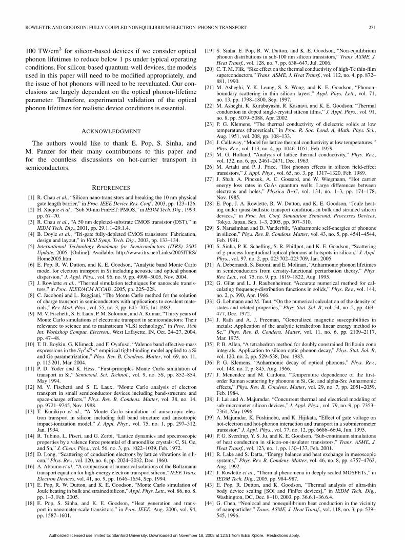
Fig. 11. Excess occupation number for the g-type longitudinal-optical (g-LO)phonon as a function of volumetric power density as calculated for (upperdashed-line data set) a uniform power generation and as calculated at (lowersolid-line data set) the peak power-generation point in the 1-D device.
indicator for hot phonons in silicon. A simple expression forthe excess occupation number, which is derived from a singlemode rate equation, is given by
ng−LO ≈Q′′′
g−LOτg−LO
�ωg−LOg(ωg−LO)∆ω(12)
where Q′′′g-LO is the volumetric power being transferred to the
g-LO phonon by the electrons in the spectral width ∆ω, andτg−LO is the modal relaxation time, which is estimated to beabout 5 ps at room temperature. This expression is valid onlyunder homogeneous power-generation conditions and tends tobe an overestimate of the population by a factor of about two.Fig. 11 shows the excess occupation number for the g-LO modeas a function of the volumetric power density for bulk siliconas well as at the hotspot of the 1-D device of Section IV. Wefind that the excess occupation number increases approximatelyas ng−LO ∼ 1 × 10⁻¹⁰Q
′′′3/4tot , where Q′′′
tot is the total volu-metric power density measured in watts per cubic centimeter.By reducing this number by a factor of 1/2 to account fornonuniform heat generation, we find that the nonequilibriumoccupation number will reach unity for a power density ofabout 20 TW/cm3. This assumes that the phonon lifetime doesnot decrease with an increasing power density. If we assumethat the phonon lifetime is reduced to subpicosecond levels athigh power densities, as some recent experimental work hasindicated it as may be likely [51], then the critical power densitywould exceed 200 TW/cm3. According to our estimates inFig. 1, this level is just beyond the projected power density forwell-behaved end-of-the-roadmap FinFET devices. Since thetransistor volumetric power density is sensitive to the fin (body)thickness, statistical process variations may cause a significantfraction of the transistors across a chip to cross into the regimewhere nonequilibrium heating plays a significant role in theelectrical transport. This may lead to an enhancement in thevariation of performance across die and wafer. In addition toa critical volumetric power density, we can estimate a criticalelectric field by relating the peak power density for ballistictransport to the peak power density given by the classical Joule
heating term as max{Q′′′ballistic} ∼ max{
⇀
J ·⇀
E}/γ, where γcan be taken to be ∼2–3 [28]. By assuming that the current
density is given by |⇀
J | ∼ β/Lg µA/nm2, where the mag-nitude of β is equivalent to the number of gate electrodes(also, ∼2–3) times 1 µA/nm, we arrive at an expression for
the critical electric field |⇀
E |crit ∼ (γ/β)max{Q′′′ballistic} · Lg .
For a 10-nm device, a critical power density of 200 TW/cm3
would correspond to a peak electric field of about 20 MV/cm,which is about 40× the field strength associated with dielectricbreakdown in silicon.
Finally, we address the consequences of our choice in usinga simplified analytic NPB model. As we mentioned brieflyin Section II, the intervalley deformation potentials used inthis paper are about twice the values computed using theFB models [12], [16]. This is despite the fact that the NPBmodel reproduces the electron DOS reasonably well up to about1.5 eV. Fischetti and Laux [12] attributed the smaller deforma-tion potentials of the FB model to the ability of the electronpopulation to reach a lower energy configuration through equiv-alent valley repopulation by means of an enhanced contributionfrom Bloch oscillation, which the NPB model fails to describeadequately. By using the NPB model, it was shown that the ratioof energy being dissipated by the optical and acoustic phononmodes is ∼2 : 1 [17]. However, the FB MC codes have shownthe reverse ratio of ∼1:2. To account for the deficiencies ofthe NPB model, we can somewhat crudely add an additionalfactor of 1/2 to (12) and increase the estimates for the onsetof the hot optical phonons to the power densities approaching500 TW/cm3. The FB calculations would undoubtedly improvethe accuracy of these estimates, but they should not changeone of the more important conclusions of this paper, that hotoptical phonons are unlikely to play a significant role in theelectrical behavior of well-behaved silicon devices describedby the existing technology roadmap.
VI. CONCLUSION
Transistor designs over the next decade will feature confinedgeometries with increasing surface-to-volume ratios and ris-ing volumetric power densities. Thermal conductance withinthe transistor will be dramatically reduced due to increasedsurface scattering and by the confinement of intrinsicallylow-conductivity materials. Furthermore, thermal boundaryresistance at interfaces between dissimilar materials, includingSi and SiGe alloys, will lead to higher junction temperaturesand, therefore, higher leakage currents than what may be ex-pected. Reliability will be impacted by the increase in junctiontemperatures caused by lower thermal conductance and mayalso be influenced by the nonequilibrium optical phonons inthe drain. Mobility reduction due to hot optical phonons doesnot seem to be a major threat to the near-term evolution ofCMOS technology. However, this assessment only stands forwell-behaved devices operating under ideal conditions throughthe end of the current roadmap. In some analog or high-powerapplications, the hot phonons could play a major role. Basedon this work, we estimate that the hot phonon effects willnot play a significant role for power densities below about
Authorized licensed use limited to: Stanford University. Downloaded on November 18, 2008 at 12:51 from IEEE Xplore. Restrictions apply.
ROWLETTE AND GOODSON: FULLY COUPLED NONEQUILIBRIUM ELECTRON–PHONON TRANSPORT 231
100 TW/cm3 for silicon-based devices if we consider opticalphonon lifetimes to reduce below 1 ps under typical operatingconditions. For silicon-based quantum-well devices, the modelsused in this paper will need to be modified appropriately, andthe issue of hot phonons will need to be reevaluated. Our con-clusions are largely dependent on the optical phonon-lifetimeparameter. Therefore, experimental validation of the opticalphonon lifetimes for realistic device conditions is essential.
ACKNOWLEDGMENT
The authors would like to thank E. Pop, S. Sinha, andM. Panzer for their many contributions to this paper andfor the countless discussions on hot-carrier transport insemiconductors.
REFERENCES
[1] R. Chau et al., “Silicon nano-transistors and breaking the 10 nm physicalgate length barrier,” in Proc. IEEE Device Res. Conf., 2003, pp. 123–126.
[2] H. Xuejue et al., “Sub 50-nm FinFET: PMOS,” in IEDM Tech. Dig., 1999,pp. 67–70.
[3] R. Chau et al., “A 50 nm depleted-substrate CMOS transistor (DST),” inIEDM Tech. Dig., 2001, pp. 29.1.1–29.1.4.
[4] B. Doyle et al., “Tri-gate fully-depleted CMOS transistors: Fabrication,design and layout,” in VLSI Symp. Tech. Dig., 2003, pp. 133–134.
[5] International Technology Roadmap for Semiconductors (ITRS) 2005Update, 2005. [Online]. Available: http://www.itrs.net/Links/2005ITRS/Home2005.htm
[6] E. Pop, R. W. Dutton, and K. E. Goodson, “Analytic band Monte Carlomodel for electron transport in Si including acoustic and optical phonondispersion,” J. Appl. Phys., vol. 96, no. 9, pp. 4998–5005, Nov. 2004.
[7] J. Rowlette et al., “Thermal simulation techniques for nanoscale transis-tors,” in Proc. IEEE/ACM ICCAD, 2005, pp. 225–228.
[8] C. Jacoboni and L. Reggiani, “The Monte Carlo method for the solutionof charge transport in semiconductors with applications to covalent mate-rials,” Rev. Mod. Phys., vol. 55, no. 3, pp. 645–705, Jul. 1983.
[9] M. V. Fischetti, S. E. Laux, P. M. Solomon, and A. Kumar, “Thirty years ofMonte Carlo simulations of electronic transport in semiconductors: Theirrelevance to science and to mainstream VLSI technology,” in Proc. 10thInt. Workshop Comput. Electron., West Lafayette, IN, Oct. 24–27, 2004,pp. 47–48.
[10] T. B. Boykin, G. Klimeck, and F. Oyafuso, “Valence band effective-massexpressions in the Sp3d5s∗ empirical tight-binding model applied to a Siand Ge parametrization,” Phys. Rev. B, Condens. Matter, vol. 69, no. 11,p. 115 201, Mar. 2004.
[11] P. D. Yoder and K. Hess, “First-principles Monte Carlo simulation oftransport in Si,” Semicond. Sci. Technol., vol. 9, no. 5S, pp. 852–854,May 1994.
[12] M. V. Fischetti and S. E. Laux, “Monte Carlo analysis of electrontransport in small semiconductor devices including band-structure andspace-charge effects,” Phys. Rev. B, Condens. Matter, vol. 38, no. 14,pp. 9721–9745, Nov. 1988.
[13] T. Kunikiyo et al., “A Monte Carlo simulation of anisotropic elec-tron transport in silicon including full band structure and anisotropicimpact-ionization model,” J. Appl. Phys., vol. 75, no. 1, pp. 297–312,Jan. 1994.
[14] R. Tubino, L. Piseri, and G. Zerbi, “Lattice dynamics and spectroscopicproperties by a valence force potential of diamondlike crystals: C, Si, Ge,and Sn,” J. Chem. Phys., vol. 56, no. 3, pp. 1022–1039, Feb. 1972.
[15] D. Long, “Scattering of conduction electrons by lattice vibrations in sili-con,” Phys. Rev., vol. 120, no. 6, pp. 2024–2032, Dec. 1960.
[16] A. Abramo et al., “A comparison of numerical solutions of the Boltzmanntransport equation for high-energy electron transport silicon,” IEEE Trans.Electron Devices, vol. 41, no. 9, pp. 1646–1654, Sep. 1994.
[17] E. Pop, R. W. Dutton, and K. E. Goodson, “Monte Carlo simulation ofJoule heating in bulk and strained silicon,” Appl. Phys. Lett., vol. 86, no. 8,pp. 1–3, Feb. 2005.
[18] E. Pop, S. Sinha, and K. E. Goodson, “Heat generation and trans-port in nanometer-scale transistors,” in Proc. IEEE, Aug. 2006, vol. 94,pp. 1587–1601.
[19] S. Sinha, E. Pop, R. W. Dutton, and K. E. Goodson, “Non-equilibriumphonon distributions in sub-100 nm silicon transistors,” Trans. ASME, J.Heat Transf., vol. 128, no. 7, pp. 638–647, Jul. 2006.
[20] C. T. M. Flik, “Size effect on the thermal conductivity of high-Tc thin-filmsuperconductors,” Trans. ASME, J. Heat Transf., vol. 112, no. 4, pp. 872–881, 1990.
[21] M. Asheghi, Y. K. Leung, S. S. Wong, and K. E. Goodson, “Phonon-boundary scattering in thin silicon layers,” Appl. Phys. Lett., vol. 71,no. 13, pp. 1798–1800, Sep. 1997.
[22] M. Asheghi, K. Kurabayashi, R. Kasnavi, and K. E. Goodson, “Thermalconduction in doped single-crystal silicon films,” J. Appl. Phys., vol. 91,no. 8, pp. 5079–5088, Apr. 2002.
[23] P. G. Klemens, “The thermal conductivity of dielectric solids at lowtemperatures (theoretical),” in Proc. R. Soc. Lond. A, Math. Phys. Sci.,Aug. 1951, vol. 208, pp. 108–133.
[24] J. Callaway, “Model for lattice thermal conductivity at low temperatures,”Phys. Rev., vol. 113, no. 4, pp. 1046–1051, Feb. 1959.
[25] M. G. Holland, “Analysis of lattice thermal conductivity,” Phys. Rev.,vol. 132, no. 6, pp. 2461–2471, Dec. 1963.
[26] M. Artaki and P. J. Price, “Hot phonon effects in silicon field-effecttransistors,” J. Appl. Phys., vol. 65, no. 3, pp. 1317–1320, Feb. 1989.
[27] J. Shah, A. Pinczuk, A. C. Gossard, and W. Wiegmann, “Hot carrierenergy loss rates in GaAs quantum wells: Large differences betweenelectrons and holes,” Physica B+C, vol. 134, no. 1–3, pp. 174–178,Nov. 1985.
[28] E. Pop, J. A. Rowlette, R. W. Dutton, and K. E. Goodson, “Joule heat-ing under quasi-ballistic transport conditions in bulk and strained silicondevices,” in Proc. Int. Conf. Simulation Semicond. Processes Devices,Tokyo, Japan, Sep. 1–3, 2005, pp. 307–310.
[29] S. Narasimhan and D. Vanderbilt, “Anharmonic self-energies of phononsin silicon,” Phys. Rev. B, Condens. Matter, vol. 43, no. 5, pp. 4541–4544,Feb. 1991.
[30] S. Sinha, P. K. Schelling, S. R. Phillpot, and K. E. Goodson, “Scatteringof g-process longitudinal optical phonons at hotspots in silicon,” J. Appl.Phys., vol. 97, no. 2, pp. 023 702–023 709, Jan. 2005.
[31] A. Debernardi, S. Baroni, and E. Molinari, “Anharmonic phonon lifetimesin semiconductors from density-functional perturbation theory,” Phys.Rev. Lett., vol. 75, no. 9, pp. 1819–1822, Aug. 1995.
[32] G. Gilat and L. J. Raubenheimer, “Accurate numerical method for cal-culating frequency-distribution functions in solids,” Phys. Rev., vol. 144,no. 2, p. 390, Apr. 1966.
[33] G. Lehmann and M. Taut, “On the numerical calculation of the density ofstates and related properties,” Phys. Stat. Sol. B, vol. 54, no. 2, pp. 469–477, Dec. 1972.
[34] J. Rath and A. J. Freeman, “Generalized magnetic susceptibilities inmetals: Application of the analytic tetrahedron linear energy method toSc,” Phys. Rev. B, Condens. Matter, vol. 11, no. 6, pp. 2109–2117,Mar. 1975.
[35] P. B. Allen, “A tetrahedron method for doubly constrained Brillouin zoneintegrals. Application to silicon optic phonon decay,” Phys. Stat. Sol. B,vol. 120, no. 2, pp. 529–538, Dec. 1983.
[36] P. G. Klemens, “Anharmonic decay of optical phonons,” Phys. Rev.,vol. 148, no. 2, p. 845, Aug. 1966.
[37] J. Menendez and M. Cardona, “Temperature dependence of the first-order Raman scattering by phonons in Si, Ge, and alpha-Sn: Anharmoniceffects,” Phys. Rev. B, Condens. Matter, vol. 29, no. 7, pp. 2051–2059,Feb. 1984.
[38] J. Lai and A. Majumdar, “Concurrent thermal and electrical modeling ofsub-micrometer silicon devices,” J. Appl. Phys., vol. 79, no. 9, pp. 7353–7361, May 1996.
[39] A. Majumdar, K. Fushinobu, and K. Hijikata, “Effect of gate voltage onhot-electron and hot-phonon interaction and transport in a submicrometertransistor,” J. Appl. Phys., vol. 77, no. 12, pp. 6686–6694, Jun. 1995.
[40] P. G. Sverdrup, Y. S. Ju, and K. E. Goodson, “Sub-continuum simulationsof heat conduction in silicon-on-insulator transistors,” Trans. ASME, J.Heat Transf., vol. 123, no. 1, pp. 130–137, Feb. 2001.
[41] R. Lake and S. Datta, “Energy balance and heat exchange in mesoscopicsystems,” Phys. Rev. B, Condens. Matter, vol. 46, no. 8, pp. 4757–4763,Aug. 1992.
[42] J. Rowlette et al., “Thermal phenomena in deeply scaled MOSFETs,” inIEDM Tech. Dig., 2005, pp. 984–987.
[43] E. Pop, R. Dutton, and K. Goodson, “Thermal analysis of ultra-thinbody device scaling [SOI and FinFet devices],” in IEDM Tech. Dig.,Washington, DC, Dec. 8–10, 2003, pp. 36.6.1–36.6.4.
[44] G. Chen, “Nonlocal and nonequilibrium heat conduction in the vicinityof nanoparticles,” Trans. ASME, J. Heat Transf., vol. 118, no. 3, pp. 539–545, 1996.
Authorized licensed use limited to: Stanford University. Downloaded on November 18, 2008 at 12:51 from IEEE Xplore. Restrictions apply.

232 IEEE TRANSACTIONS ON ELECTRON DEVICES, VOL. 55, NO. 1, JANUARY 2008
[45] G. Chen, “Ballistic-diffusive heat-conduction equations,” Phys. Rev. Lett.,vol. 86, no. 11, pp. 2297–2300, Mar. 2001.
[46] Y. Wang, K. P. Cheung, A. S. Oates, and P. Mason, “Ballistic phononenhanced NBTI,” in Proc. IEEE Int. Rel. Phys. Symp., Phoenix, AZ, 2007,pp. 258–263.
[47] S. Polonsky and K. A. Jenkins, “Time-resolved measurements of self-heating in SOI and strained-Si MOSFETs using off-state leakage currentluminescence,” in Proc. Int. Semicond. Device Res. Symp., Washington,DC, Dec. 10–12, 2003, pp. 359–360.
[48] A. R. Vasconcellos, R. Luzzi, C. G. Rodrigues, and V. N. Freire, “Hot-phonon bottleneck in the photoinjected plasma in GaN,” Appl. Phys. Lett.,vol. 82, no. 15, pp. 2455–2457, Apr. 2003.
[49] J. Liberis et al., “Hot phonons in Si-doped GaN,” Appl. Phys. Lett.,vol. 89, no. 20, p. 202 117, Nov. 2006.
[50] E. Pop et al., “Negative differential conductance and hot phonons insuspended nanotube molecular wires,” Phys. Rev. Lett., vol. 95, no. 15,pp. 155 504–155 505, Oct. 2005.
[51] J. J. Letcher, K. Kang, D. G. Cahill, and D. D. Dlott, “Effects of highcarrier densities on phonon and carrier lifetimes in Si by time-resolvedanti-Stokes Raman scattering,” Appl. Phys. Lett., vol. 90, no. 25,pp. 252 103–252 104, Jun. 2007.
Jeremy A. Rowlette received the B.S.E.E. degreefrom the Pennsylvania State University, UniversityPark, in 2000 and the M.S.E.E. degree from StanfordUniversity, Stanford, CA, in 2005. He is currentlyworking toward the Ph.D. degree in electrical engi-neering at Stanford University. His Ph.D. research isthe study of electrothermal and optoelectronic phe-nomena in low-dimensional semiconductors, whichis supported by an Intel Graduate Fellowship. From2000 to 2004, his graduate studies were supported bythe Intel Honors Cooperative Program.
Prior to his doctoral work, Jeremy spent five years, from 1999 to 2004, withthe Intel Corporation, developing optical and ion-beam-based circuit diagnosticequipment for microprocessors and flash memory. His interests include solid-state physics and photonics, optical-electronic design, and experimental optics.
Kenneth E. Goodson received the Ph.D. degreein mechanical engineering from the MassachusettsInstitute of Technology, Cambridge, in 1993.
He spent two years with the Materials Group,Daimler-Benz AG. He is a Professor of mechani-cal engineering with the Department of Mechani-cal Engineering, Stanford University, Stanford, CA,where his group studies nanoscale-transport phe-nomena relevant for electronic systems. His Stanfordresearch group includes 15 students and research as-sociates studying thermal-transport phenomena rel-
evant for electronic systems, with a focus on those occurring with very smalllength and time scales. He is a Cofounder and Former Chief Technology Officerof Cooligy, which develops microfluidic cooling technology for computers. Hehas authored or coauthored more than 120 journal and conference papers andfive book chapters.
Dr. Goodson’s group has been recognized through the Office of NavalResearch Young Investigator Award, the NSF CAREER Award, the Journalof Heat Transfer Outstanding Reviewer Award in 1999, a Japan Society forthe Promotion of Science Visiting Professorship at the Tokyo Institute ofTechnology, Tokyo, Japan, in 1996, as well as the Best Paper Awards atthe SEMI-THERM, the Multilevel Interconnect Symposium, and the SRCTECHCON.
Authorized licensed use limited to: Stanford University. Downloaded on November 18, 2008 at 12:51 from IEEE Xplore. Restrictions apply.