full-featured, low pin count microcontrollers with xlp · • idle mode: ability to put the cpu...
TRANSCRIPT
PIC16(L)F18324/18344Full-Featured, Low Pin Count Microcontrollers with XLP
Description
PIC16(L)F18324/18344 microcontrollers feature Analog, Core Independent Peripherals and CommunicationPeripherals, combined with eXtreme Low Power (XLP) for a wide range of general purpose and low-power applications.The Peripheral Pin Select (PPS) functionality enables pin mapping when using the digital peripherals (CLC, CWG, CCP,PWM and communications) to add flexibility to the application design.
Core Features
• C Compiler Optimized RISC Architecture• Only 48 Instructions• Operating Speed:
- DC – 32 MHz clock input- 125 ns minimum instruction cycle
• Interrupt Capability • 16-Level Deep Hardware Stack• Up to Four 8-Bit Timers• Up to Three 16-Bit Timers• Low-Current Power-on Reset (POR)• Power-up Timer (PWRTE)• Brown-out Reset (BOR)• Low-Power BOR (LPBOR) Option• Extended Watchdog Timer (WDT) with Dedicated
On-Chip Oscillator for Reliable Operation• Programmable Code Protection
Memory
• 7 Kbytes Program Flash Memory• 512 Bytes Data SRAM Memory • 256B of EEPROM• Direct, Indirect and Relative Addressing modes
Operating Characteristics
• Operating Voltage Range:- 1.8V to 3.6V (PIC16LF18324/18344)- 2.3V to 5.5V (PIC16F18324/18344)
• Temperature Range:- Industrial: -40°C to 85°C- Extended: -40°C to 125°C
eXtreme Low-Power (XLP) Features
• Sleep mode: 40 nA @ 1.8V, typical • Watchdog Timer: 250 nA @ 1.8V, typical • Secondary Oscillator: 300 nA @ 32 kHz • Operating Current:
- 8 A @ 32 kHz, 1.8V, typical - 37 A/MHz @ 1.8V, typical
Power-Saving Functionality
• IDLE mode: ability to put the CPU core to Sleep while internal peripherals continue operating from the system clock
• DOZE mode: ability to run the CPU core slower than the system clock used by the internal peripherals
• SLEEP mode: Lowest Power Consumption• Peripheral Module Disable (PMD): peripheral
power disable hardware module to minimize power consumption of unused peripherals
Digital Peripherals
• Configurable Logic Cell (CLC): - Four CLCs- Integrated combinational and sequential logic
• Complementary Waveform Generator (CWG):- Two CWGs- Rising and falling edge dead-band control- Full-bridge, half-bridge, 1-channel drive- Multiple signal sources
• Capture/Compare/PWM (CCP) modules- Four CCPs- 16-bit resolution for Capture/Compare modes- 10-bit resolution for PWM mode
• Pulse-Width Modulators (PWM):- Two 10-bit PWMs
• Numerically Controlled Oscillator (NCO):- Precision linear frequency generator (@50%
duty cycle) with 0.0001% step size of source input clock
- Input Clock: 0 Hz < FNCO < 32 MHz- Resolution: FNCO/220
• Serial Communications:- EUSART
- RS-232, RS-485, LIN compatible- Auto-Baud Detect, auto-wake-up on start
- Master Synchronous Serial Port (MSSP)- SPI- I2C, SMBus, PMBus™ compatible
• Data Signal Modulator (DSM):- Modulates a carrier signal with digital data to
create custom carrier synchronized output waveforms
2015-2016 Microchip Technology Inc. Preliminary DS40001800B-page 1
PIC16(L)F18324/18344
• Up to 18 I/O Pins:- Individually programmable pull-ups - Slew rate control - Interrupt-on-change with edge-select- Input level selection control (ST or TTL)- Digital open-drain enable
• Peripheral Pin Select (PPS): - I/O pin remapping of digital peripherals
• Timer modules:- Timer0:
- 8/16-bit timer/counter- Synchronous or asynchronous operation- Programmable prescaler/postscaler- Time base for capture/compare function
- Timer1/3/5 with gate control:- 16-bit timer/counter- Programmable internal or external clock
sources- Multiple gate sources- Multiple gate modes- Time base for capture/compare function
- Timer2/4/6:- 8-bit timers- Programmable prescaler/postscaler- Time base for PWM function
Analog Peripherals
• 10-Bit Analog-to-Digital Converter (ADC):- 17 external channels- Conversion available during Sleep
• Comparator:- Two comparators- Fixed Voltage Reference at non-inverting
input(s) - Comparator outputs externally accessible
• 5-Bit Digital-to-Analog Converter (DAC):- 5-bit resolution, rail-to-rail- Positive Reference Selection - Unbuffered I/O pin output - Internal connections to ADCs and
comparators• Voltage Reference:
- Fixed Voltage Reference with 1.024V, 2.048V and 4.096V output levels
Flexible Oscillator Structure
• High-Precision Internal Oscillator:- Software-selectable frequency range up to 32
MHz- ±2% at nominal 4 MHz calibration point
• 4x PLL with External Sources• Low-Power Internal 31 kHz Oscillator
(LFINTOSC)• External Low-power 32 kHz Crystal Oscillator
(SOSC)• External Oscillator Block with:
- Three Crystal/Resonator modes up to 20 MHz
- Three External Clock modes up to 20 MHz- Fail-Safe Clock Monitor:
- Detects clock source failure- Oscillator Start-up Timer (OST)
- Ensures stability of crystal oscillator sources
2015-2016 Microchip Technology Inc. Preliminary DS40001800B-page 2
PIC16(L)F18324/18344
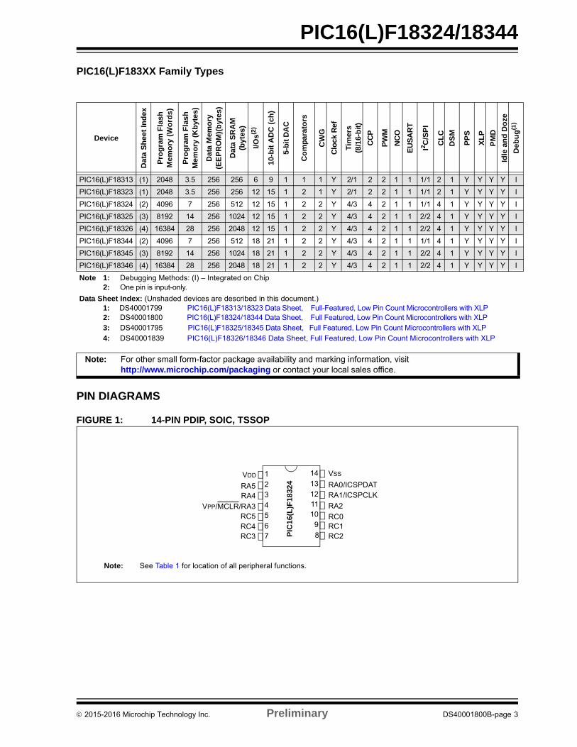
PIC16(L)F183XX Family Types
PIN DIAGRAMS
FIGURE 1: 14-PIN PDIP, SOIC, TSSOP
DeviceD
ata
Sh
ee
t In
de
x
Pro
gra
m F
las
h
Me
mo
ry (
Wo
rds
)
Pro
gra
m F
las
h
Me
mo
ry (
Kb
yte
s)
Da
ta M
em
ory
(EE
PR
OM
)(b
yte
s)
Da
ta S
RA
M(b
yte
s)
I/O
s(2
)
10
-bit
AD
C (
ch
)
5-b
it D
AC
Co
mp
ara
tors
CW
G
Clo
ck R
ef
Tim
ers
(8/1
6-b
it)
CC
P
PW
M
NC
O
EU
SA
RT
I2 C/S
PI
CL
C
DS
M
PP
S
XL
P
PM
D
Idle
an
d D
oze
De
bu
g(1
)
PIC16(L)F18313 (1) 2048 3.5 256 256 6 9 1 1 1 Y 2/1 2 2 1 1 1/1 2 1 Y Y Y Y I
PIC16(L)F18323 (1) 2048 3.5 256 256 12 15 1 2 1 Y 2/1 2 2 1 1 1/1 2 1 Y Y Y Y I
PIC16(L)F18324 (2) 4096 7 256 512 12 15 1 2 2 Y 4/3 4 2 1 1 1/1 4 1 Y Y Y Y I
PIC16(L)F18325 (3) 8192 14 256 1024 12 15 1 2 2 Y 4/3 4 2 1 1 2/2 4 1 Y Y Y Y I
PIC16(L)F18326 (4) 16384 28 256 2048 12 15 1 2 2 Y 4/3 4 2 1 1 2/2 4 1 Y Y Y Y I
PIC16(L)F18344 (2) 4096 7 256 512 18 21 1 2 2 Y 4/3 4 2 1 1 1/1 4 1 Y Y Y Y I
PIC16(L)F18345 (3) 8192 14 256 1024 18 21 1 2 2 Y 4/3 4 2 1 1 2/2 4 1 Y Y Y Y I
PIC16(L)F18346 (4) 16384 28 256 2048 18 21 1 2 2 Y 4/3 4 2 1 1 2/2 4 1 Y Y Y Y I
Note 1: Debugging Methods: (I) – Integrated on Chip2: One pin is input-only.
Data Sheet Index: (Unshaded devices are described in this document.)1: DS40001799 PIC16(L)F18313/18323 Data Sheet, Full-Featured, Low Pin Count Microcontrollers with XLP2: DS40001800 PIC16(L)F18324/18344 Data Sheet, Full Featured, Low Pin Count Microcontrollers with XLP3: DS40001795 PIC16(L)F18325/18345 Data Sheet, Full Featured, Low Pin Count Microcontrollers with XLP4: DS40001839 PIC16(L)F18326/18346 Data Sheet, Full Featured, Low Pin Count Microcontrollers with XLP
Note: For other small form-factor package availability and marking information, visithttp://www.microchip.com/packaging or contact your local sales office.
1234567
VDD
RA5RA4
VPP/MCLR/RA3RC5RC4RC3
RA0/ICSPDATRA1/ICSPCLK
RA2
RC0RC1RC2
14
13121110
9
8
VSS
PIC
16
(L)F
18
32
4
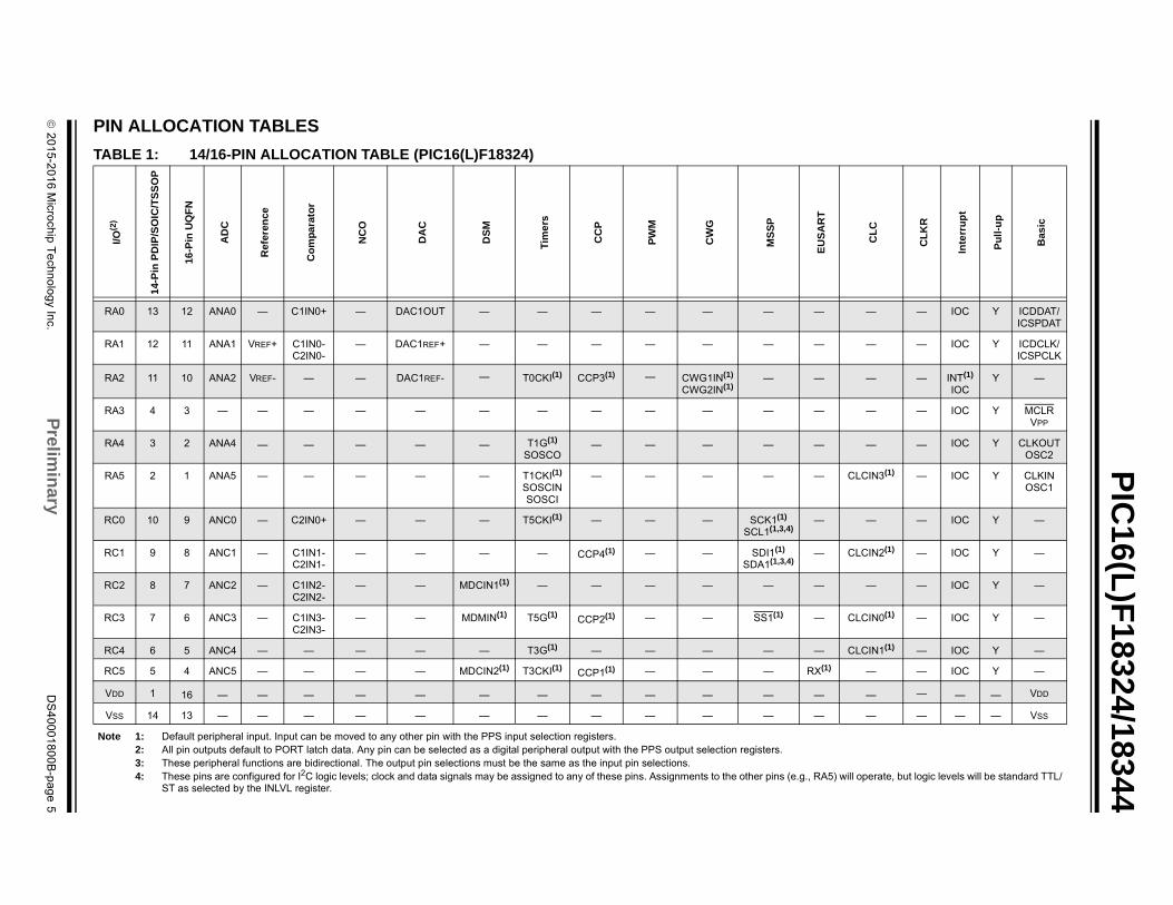
Note: See Table 1 for location of all peripheral functions.
2015-2016 Microchip Technology Inc. Preliminary DS40001800B-page 3
PIC16(L)F18324/18344
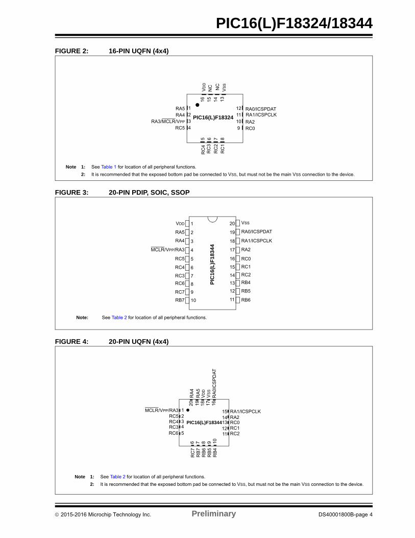
FIGURE 2: 16-PIN UQFN (4x4)
FIGURE 3: 20-PIN PDIP, SOIC, SSOP
FIGURE 4: 20-PIN UQFN (4x4)
23
1
9
10
1112
RC
4
4
VS
S
RA0/ICSPDATRA1/ICSPCLK
RA2RC0
NC
NC
VD
D
RA5RA4
RA3/MCLR/VPP
RC5
RC
3
RC
2
RC
1
6 75 8
15 1416 13
PIC16(L)F18324
Note 1: See Table 1 for location of all peripheral functions.
2: It is recommended that the exposed bottom pad be connected to VSS, but must not be the main VSS connection to the device.
PIC
16
(L)F
18
34
4
2
3
4
5
6
7
8
9
10
VDD
RA5
RA4
MCLR/VPP/RA3
RC5
RC4
RC3
RC6
RC7
RB7
RA0/ICSPDAT
RA1/ICSPCLK
RA2
RC0
RC1
RC2
RB4
RB5
RB6
20
19
18
17
16
15
14
13
12
11
VSS1
Note: See Table 2 for location of all peripheral functions.
2345
1
6 7 8 9
20 19 18 17 1610
12131415
11
PIC16(L)F18344
RB
4R
B5
RB
6R
B7
RC
7
MCLR/VPP/RA3RC5RC4RC3RC6
RA
4R
A5
VD
D
VS
S
RA
0IC
SP
DA
T
RA1/ICSPCLKRA2RC0RC1RC2
Note 1: See Table 2 for location of all peripheral functions.
2: It is recommended that the exposed bottom pad be connected to VSS, but must not be the main VSS connection to the device.
2015-2016 Microchip Technology Inc. Preliminary DS40001800B-page 4
2
01
5-2
01
6 M
icroch
ip T
ech
no
log
y Inc.
Prelim
inary
DS
40
00
18
00
B-p
ag
e 5
PIC
16(L)F
18324/18344
PI
TA
CL
C
CL
KR
Inte
rru
pt
Pu
ll-u
p
Bas
ic
R — — IOC Y ICDDAT/ICSPDAT
R — — IOC Y ICDCLK/ICSPCLK
R — — INT(1)
IOCY —
R — — IOC Y MCLRVPP
R — — IOC Y CLKOUTOSC2
R CLCIN3(1) — IOC Y CLKINOSC1
R — — IOC Y —
R CLCIN2(1) — IOC Y —
R — — IOC Y —
R CLCIN0(1) — IOC Y —
R CLCIN1(1) — IOC Y —
R — — IOC Y —
V — — — — VDD
V — — — — VSS
No
) will operate, but logic levels will be standard TTL/
N ALLOCATION TABLES
BLE 1: 14/16-PIN ALLOCATION TABLE (PIC16(L)F18324)
I/O
(2)
14-
Pin
PD
IP/S
OIC
/TS
SO
P
16-P
in U
QF
N
AD
C
Ref
eren
ce
Co
mp
arat
or
NC
O
DA
C
DS
M
Tim
ers
CC
P
PW
M
CW
G
MS
SP
EU
SA
RT
A0 13 12 ANA0 — C1IN0+ — DAC1OUT — — — — — — —
A1 12 11 ANA1 VREF+ C1IN0-C2IN0-
— DAC1REF+ — — — — — — —
A2 11 10 ANA2 VREF- — — DAC1REF- — T0CKI(1) CCP3(1) — CWG1IN(1)
CWG2IN(1)— —
A3 4 3 — — — — — — — — — — — —
A4 3 2 ANA4 — — — — — T1G(1)
SOSCO— — — — —
A5 2 1 ANA5 — — — — — T1CKI(1)
SOSCINSOSCI
— — — — —
C0 10 9 ANC0 — C2IN0+ — — — T5CKI(1) — — — SCK1(1)
SCL1(1,3,4)—
C1 9 8 ANC1 — C1IN1-C2IN1-
— — — — CCP4(1) — — SDI1(1)
SDA1(1,3,4)—
C2 8 7 ANC2 — C1IN2-C2IN2-
— — MDCIN1(1) — — — — — —
C3 7 6 ANC3 — C1IN3-C2IN3-
— — MDMIN(1) T5G(1) CCP2(1) — — SS1(1) —
C4 6 5 ANC4 — — — — — T3G(1) — — — — —
C5 5 4 ANC5 — — — — MDCIN2(1) T3CKI(1) CCP1(1) — — — RX(1)
DD 1 16 — — — — — — — — — — — —
SS 14 13 — — — — — — — — — — — —
te 1: Default peripheral input. Input can be moved to any other pin with the PPS input selection registers.2: All pin outputs default to PORT latch data. Any pin can be selected as a digital peripheral output with the PPS output selection registers.3: These peripheral functions are bidirectional. The output pin selections must be the same as the input pin selections.4: These pins are configured for I2C logic levels; clock and data signals may be assigned to any of these pins. Assignments to the other pins (e.g., RA5
ST as selected by the INLVL register.
2
01
5-2
01
6 M
icroch
ip T
ech
no
log
y Inc.
Prelim
inary
DS
40
00
18
00
B-p
ag
e 6
PIC
16(L)F
18324/18344
O
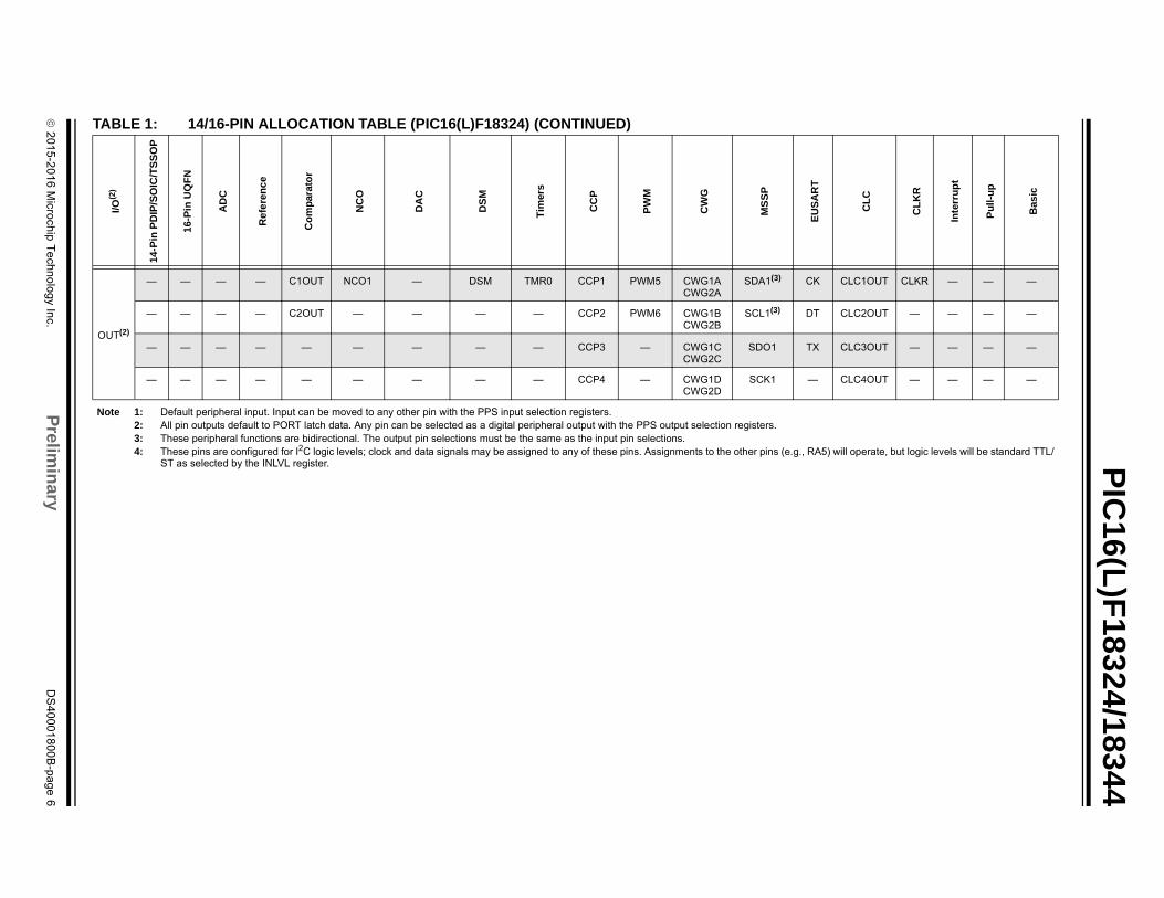
CLC1OUT CLKR — — —
CLC2OUT — — — —
CLC3OUT — — — —
CLC4OUT — — — —
TA
CL
C
CL
KR
Inte
rru
pt
Pu
ll-u
p
Bas
ic
No
5) will operate, but logic levels will be standard TTL/
UT(2)
— — — — C1OUT NCO1 — DSM TMR0 CCP1 PWM5 CWG1ACWG2A
SDA1(3) CK
— — — — C2OUT — — — — CCP2 PWM6 CWG1BCWG2B
SCL1(3) DT
— — — — — — — — — CCP3 — CWG1CCWG2C
SDO1 TX
— — — — — — — — — CCP4 — CWG1DCWG2D
SCK1 —
BLE 1: 14/16-PIN ALLOCATION TABLE (PIC16(L)F18324) (CONTINUED)I/O
(2)
14-P
in P
DIP
/SO
IC/T
SS
OP
16-
Pin
UQ
FN
AD
C
Ref
ere
nc
e
Co
mp
arat
or
NC
O
DA
C
DS
M
Tim
ers
CC
P
PW
M
CW
G
MS
SP
EU
SA
RT
te 1: Default peripheral input. Input can be moved to any other pin with the PPS input selection registers.2: All pin outputs default to PORT latch data. Any pin can be selected as a digital peripheral output with the PPS output selection registers.3: These peripheral functions are bidirectional. The output pin selections must be the same as the input pin selections.4: These pins are configured for I2C logic levels; clock and data signals may be assigned to any of these pins. Assignments to the other pins (e.g., RA
ST as selected by the INLVL register.
2
01
5-2
01
6 M
icroch
ip T
ech
no
log
y Inc.
Prelim
inary
DS
40
00
18
00
B-p
ag
e 7
PIC
16(L)F
18324/18344
TA
CL
C
CL
KR
Inte
rru
pt
Pu
ll-u
p
Ba
sic
— — IOC Y ICDDAT ICSPDAT
— — IOC Y ICDCLKICSPCLK
CLCIN0(1) — IOCINT(1)
Y —
— — IOC Y MCLRVPP
— — IOC Y CLKOUTOSC2
— — IOC Y CLKINOSC1
CLCIN2(1) — IOC Y —
) CLCIN3(1) — IOC Y —
— — IOC Y —
— — IOC Y —
— — IOC Y —
— — IOC Y —
— — IOC Y —
CLCIN1(1) — IOC Y —
No
ill operate, but logic levels will be standard TTL/ST
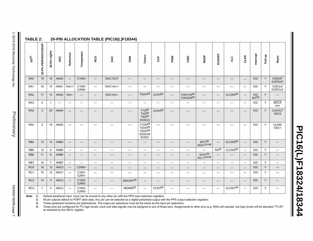
BLE 2: 20-PIN ALLOCATION TABLE (PIC16(L)F18344)
I/O(2
)
20-
Pin
PD
IP/S
OIC
/SS
OP
20-P
in U
QF
N
AD
C
Re
fere
nce
Co
mp
ara
tor
NC
O
DA
C
DS
M
Tim
ers
CC
P
PW
M
CW
G
MS
SP
EU
SA
RT
RA0 19 16 ANA0 — C1IN0+ — DAC1OUT — — — — — — —
RA1 18 15 ANA1 VREF+ C1IN0-C2IN0-
— DAC1REF+ — — — — — — —
RA2 17 14 ANA2 VREF- — — DAC1REF- — T0CKI(1) CCP3(1) — CWG1IN(1)
CWG2IN(1)— —
RA3 4 1 — — — — — — — — — — — —
RA4 3 20 ANA4 — — — — — T1G(1)
T3G(1)
T5G(1)
SOSCO
CCP4(1) — — — —
RA5 2 19 ANA5 — — — — — T1CKI(1)
T3CKI(1)
T5CKI(1)
SOSCINSOSCI
— — — — —
RB4 13 10 ANB4 — — — — — — — — — SDI1(1)
SDA1(1,3,4)—
RB5 12 9 ANB5 — — — — — — — — — — RX(1
RB6 11 8 ANB6 — — — — — — — — — SCK1(1)
SCL1(1,3,4)—
RB7 10 7 ANB7 — — — — — — — — — — —
RC0 16 13 ANC0 — C2IN0+ — — — — — — — — —
RC1 15 12 ANC1 — C1IN1-C2IN1-
— — — — — — — — —
RC2 14 11 ANC2 — C1IN2-C2IN2-
— — MDCIN1(1) — — — — — —
RC3 7 4 ANC3 — C1IN3-C2IN3-
— — MDMIN(1) — CCP2(1) — — — —
te 1: Default peripheral input. Input can be moved to any other pin with the PPS input selection registers.2: All pin outputs default to PORT latch data. Any pin can be selected as a digital peripheral output with the PPS output selection registers.3: These peripheral functions are bidirectional. The output pin selections must be the same as the input pin selections.4: These pins are configured for I2C logic levels; clock and data signals may be assigned to any of these pins. Assignments to other pins (e.g. RA5) w
as selected by the INLVL register.
2
01
5-2
01
6 M
icroch
ip T
ech
no
log
y Inc.
Prelim
inary
DS
40
00
18
00
B-p
ag
e 8
PIC
16(L)F
18324/18344
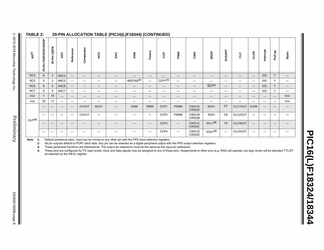
— — IOC Y —
— — IOC Y —
— — IOC Y —
— — IOC Y —
— — — — VDD
— — — — VSS
O
CLC1OUT CLKR — — —
CLC2OUT — — — —
CLC3OUT — — — —
CLC4OUT — — — —
TA
CL
C
CL
KR
Inte
rru
pt
Pu
ll-u
p
Ba
sic
No
ill operate, but logic levels will be standard TTL/ST
RC4 6 3 ANC4 — — — — — — — — — — —
RC5 5 2 ANC5 — — — — MDCIN2(1) — CCP1(1) — — — —
RC6 8 5 ANC6 — — — — — — — — — SS1(1) —
RC7 9 6 ANC7 — — — — — — — — — — —
VDD 1 18 — — — — — — — — — — — —
VSS 20 17 — — — — — — — — — — — —
UT(2)
— — — — C1OUT NCO1 — DSM TMR0 CCP1 PWM5 CWG1ACWG2A
SDO1 DT
— — — — C2OUT — — — — CCP2 PWM6 CWG1BCWG2B
SCK1 CK
— — — — — — — — — CCP3 — CWG1CCWG2C
SCL1(3) TX
— — — — — — — — — CCP4 — CWG1DCWG2D
SDA1(3) —
BLE 2: 20-PIN ALLOCATION TABLE (PIC16(L)F18344) (CONTINUED)I/O
(2)
20-
Pin
PD
IP/S
OIC
/SS
OP
20-P
in U
QF
N
AD
C
Re
fere
nce
Co
mp
ara
tor
NC
O
DA
C
DS
M
Tim
ers
CC
P
PW
M
CW
G
MS
SP
EU
SA
RT
te 1: Default peripheral input. Input can be moved to any other pin with the PPS input selection registers.2: All pin outputs default to PORT latch data. Any pin can be selected as a digital peripheral output with the PPS output selection registers.3: These peripheral functions are bidirectional. The output pin selections must be the same as the input pin selections.4: These pins are configured for I2C logic levels; clock and data signals may be assigned to any of these pins. Assignments to other pins (e.g. RA5) w
as selected by the INLVL register.

PIC16(L)F18324/18344
Table of Contents
1.0 Device Overview ........................................................................................................................................................................ 112.0 Guidelines for Getting Started With PIC16(L)F183XX Microcontrollers ..................................................................................... 203.0 Enhanced Mid-Range CPU ........................................................................................................................................................ 234.0 Memory Organization ................................................................................................................................................................. 255.0 Device Configuration .................................................................................................................................................................. 616.0 Resets ........................................................................................................................................................................................ 687.0 Oscillator Module........................................................................................................................................................................ 778.0 Interrupts .................................................................................................................................................................................... 949.0 Power-Saving Operation Modes .............................................................................................................................................. 11010.0 Watchdog Timer (WDT) ........................................................................................................................................................... 11611.0 Nonvolatile Memory (NVM) Control.......................................................................................................................................... 12012.0 I/O Ports ................................................................................................................................................................................... 13713.0 Peripheral Pin Select (PPS) Module ........................................................................................................................................ 15614.0 Peripheral Module Disable ....................................................................................................................................................... 16315.0 Interrupt-on-Change ................................................................................................................................................................. 16916.0 Fixed Voltage Reference (FVR) .............................................................................................................................................. 17617.0 Temperature Indicator Module ................................................................................................................................................. 17918.0 Comparator Module.................................................................................................................................................................. 18119.0 Pulse-Width Modulation (PWM) ............................................................................................................................................... 19020.0 Complementary Waveform Generator (CWG) Module ............................................................................................................ 19621.0 Configurable Logic Cell (CLC).................................................................................................................................................. 21822.0 Analog-to-Digital Converter (ADC) Module .............................................................................................................................. 23323.0 Numerically Controlled Oscillator (NCO1)................................................................................................................................ 24724.0 5-Bit Digital-to-Analog Converter (DAC1) Module.................................................................................................................... 25825.0 Data Signal Modulator (DSM) Module...................................................................................................................................... 26226.0 Timer0 Module ......................................................................................................................................................................... 27327.0 Timer1/3/5 Module with Gate Control....................................................................................................................................... 28128.0 Timer2/4/6 Module ................................................................................................................................................................... 29429.0 Capture/Compare/PWM Modules ............................................................................................................................................ 29530.0 Master Synchronous Serial Port (MSSP1) Module .................................................................................................................. 31131.0 Enhanced Universal Synchronous Asynchronous Receiver Transmitter (EUSART1) ............................................................. 36532.0 Reference Clock Output Module .............................................................................................................................................. 39033.0 In-Circuit Serial Programming™ (ICSP™) ............................................................................................................................... 39434.0 Instruction Set Summary .......................................................................................................................................................... 39635.0 Electrical Specifications............................................................................................................................................................ 41036.0 DC and AC Characteristics Graphs and Charts ....................................................................................................................... 43937.0 Development Support............................................................................................................................................................... 44038.0 Packaging Information.............................................................................................................................................................. 444The Microchip Website ...................................................................................................................................................................... 467Customer Change Notification Service .............................................................................................................................................. 467Customer Support .............................................................................................................................................................................. 467Product Identification System ............................................................................................................................................................ 468
2015-2016 Microchip Technology Inc. Preliminary DS40001800B-page 9

PIC16(L)F18324/18344
TO OUR VALUED CUSTOMERS
It is our intention to provide our valued customers with the best documentation possible to ensure successful use of your Microchipproducts. To this end, we will continue to improve our publications to better suit your needs. Our publications will be refined andenhanced as new volumes and updates are introduced.
If you have any questions or comments regarding this publication, please contact the Marketing Communications Department viaE-mail at [email protected]. We welcome your feedback.
Most Current Data Sheet
To obtain the most up-to-date version of this data sheet, please register at our Worldwide Website at:
http://www.microchip.com
You can determine the version of a data sheet by examining its literature number found on the bottom outside corner of any page.The last character of the literature number is the version number, (e.g., DS30000000A is version A of document DS30000000).
Errata
An errata sheet, describing minor operational differences from the data sheet and recommended workarounds, may exist for currentdevices. As device/documentation issues become known to us, we will publish an errata sheet. The errata will specify the revisionof silicon and revision of document to which it applies.
To determine if an errata sheet exists for a particular device, please check with one of the following:
• Microchip’s Worldwide Website; http://www.microchip.com• Your local Microchip sales office (see last page)When contacting a sales office, please specify which device, revision of silicon and data sheet (include literature number) you areusing.
Customer Notification System
Register on our website at www.microchip.com to receive the most current information on all of our products.
2015-2016 Microchip Technology Inc. Preliminary DS40001800B-page 10
PIC16(L)F18324/18344
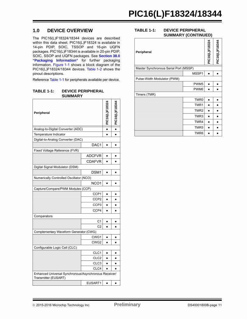
1.0 DEVICE OVERVIEW
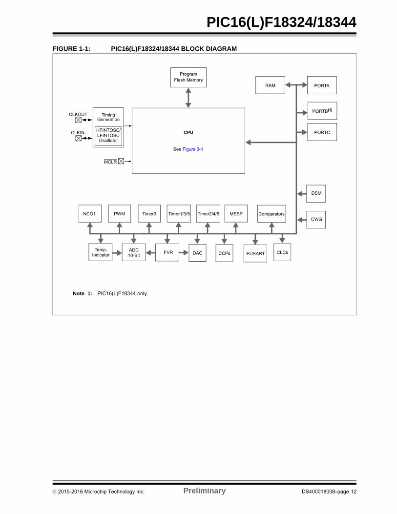
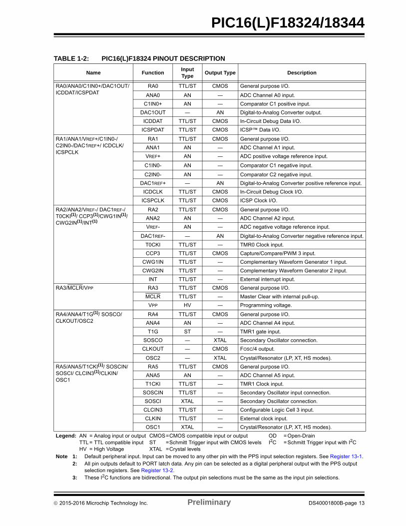
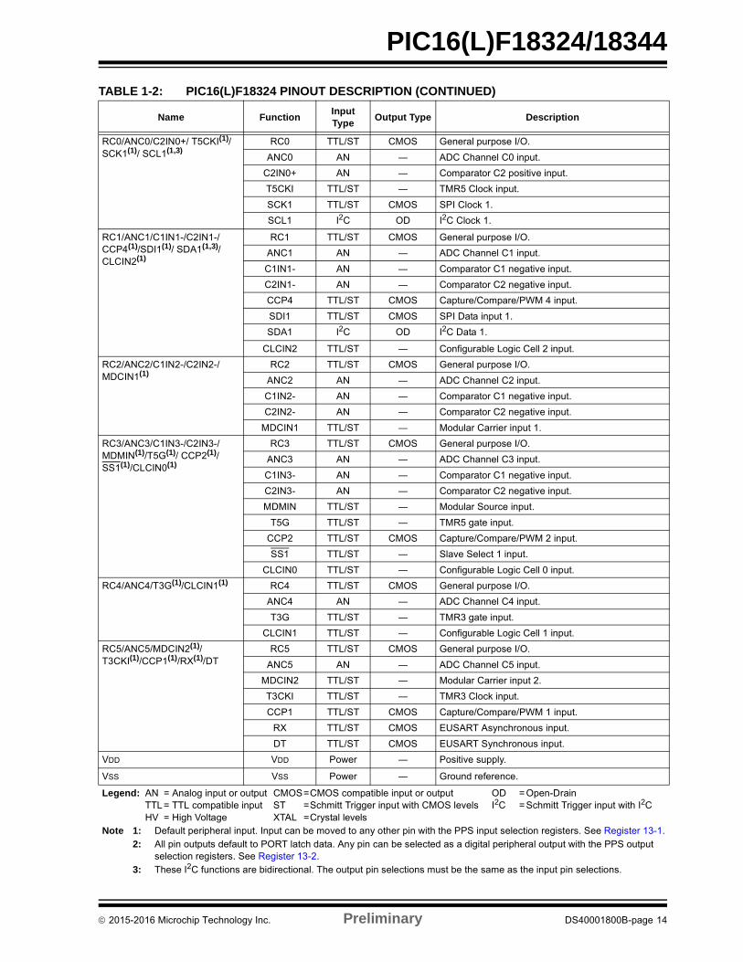
The PIC16(L)F18324/18344 devices are describedwithin this data sheet. PIC16(L)F18324 is available in14-pin PDIP, SOIC, TSSOP and 16-pin UQFNpackages. PIC16(L)F18344 is available in 20-pin PDIP,SOIC, SSOP and UQFN packages. See Section 38.0“Packaging Information” for further packaginginformation. Figure 1-1 shows a block diagram of thePIC16(L)F18324/18344 devices. Table 1-2 shows thepinout descriptions.
Reference Table 1-1 for peripherals available per device.
TABLE 1-1: DEVICE PERIPHERAL SUMMARY
Peripheral
PIC
16
(L)F
18
32
4
PIC
16
(L)F
18
34
4
Analog-to-Digital Converter (ADC)
Temperature Indicator
Digital-to-Analog Converter (DAC)
DAC1
Fixed Voltage Reference (FVR)
ADCFVR
CDAFVR
Digital Signal Modulator (DSM)
DSM1
Numerically Controlled Oscillator (NCO)
NCO1
Capture/Compare/PWM Modules (CCP)
CCP1
CCP2
CCP3
CCP4
Comparators
C1
C2
Complementary Waveform Generator (CWG)
CWG1
CWG2
Configurable Logic Cell (CLC)
CLC1
CLC2
CLC3
CLC4
Enhanced Universal Synchronous/Asynchronous Receiver/Transmitter (EUSART)
EUSART1
Master Synchronous Serial Port (MSSP)
MSSP1
Pulse-Width Modulator (PWM)
PWM5
PWM6
Timers (TMR)
TMR0
TMR1
TMR2
TMR3
TMR4
TMR5
TMR6
TABLE 1-1: DEVICE PERIPHERAL SUMMARY (CONTINUED)
Peripheral
PIC
16
(L)F
18
32
4
PIC
16
(L)F
18
34
4
2015-2016 Microchip Technology Inc. Preliminary DS40001800B-page 11
PIC16(L)F18324/18344
FIGURE 1-1: PIC16(L)F18324/18344 BLOCK DIAGRAM
PORTA
PORTCCPU
ProgramFlash Memory
RAM
TimingGeneration
LFINTOSCOscillator
MCLR
CLKIN
CLKOUT
ADC10-Bit
FVRTemp.
Indicator EUSART
ComparatorsMSSPTimer2/4/6Timer1/3/5Timer0
DAC CCPs
PWMNCO1
HFINTOSC/
CLCs
CWG
DSM
Note 1: PIC16(L)F18344 only.
PORTB(1)
See Figure 3-1
2015-2016 Microchip Technology Inc. Preliminary DS40001800B-page 12
PIC16(L)F18324/18344
TABLE 1-2: PIC16(L)F18324 PINOUT DESCRIPTION
Name FunctionInput Type
Output Type Description
RA0/ANA0/C1IN0+/DAC1OUT/ ICDDAT/ICSPDAT
RA0 TTL/ST CMOS General purpose I/O.
ANA0 AN ― ADC Channel A0 input.
C1IN0+ AN ― Comparator C1 positive input.
DAC1OUT ― AN Digital-to-Analog Converter output.
ICDDAT TTL/ST CMOS In-Circuit Debug Data I/O.
ICSPDAT TTL/ST CMOS ICSP™ Data I/O.
RA1/ANA1/VREF+/C1IN0-/C2IN0-/DAC1REF+/ ICDCLK/ICSPCLK
RA1 TTL/ST CMOS General purpose I/O.
ANA1 AN ― ADC Channel A1 input.
VREF+ AN ― ADC positive voltage reference input.
C1IN0- AN ― Comparator C1 negative input.
C2IN0- AN ― Comparator C2 negative input.
DAC1REF+ ― AN Digital-to-Analog Converter positive reference input.
ICDCLK TTL/ST CMOS In-Circuit Debug Clock I/O.
ICSPCLK TTL/ST CMOS ICSP Clock I/O.
RA2/ANA2/VREF-/ DAC1REF-/T0CKI(1)/ CCP3(1)/CWG1IN(1)/ CWG2IN(1)/INT(1)
RA2 TTL/ST CMOS General purpose I/O.
ANA2 AN ― ADC Channel A2 input.
VREF- AN ― ADC negative voltage reference input.
DAC1REF- ― AN Digital-to-Analog Converter negative reference input.
T0CKI TTL/ST ― TMR0 Clock input.
CCP3 TTL/ST CMOS Capture/Compare/PWM 3 input.
CWG1IN TTL/ST ― Complementary Waveform Generator 1 input.
CWG2IN TTL/ST ― Complementary Waveform Generator 2 input.
INT TTL/ST ― External interrupt input.
RA3/MCLR/VPP RA3 TTL/ST CMOS General purpose I/O.
MCLR TTL/ST ― Master Clear with internal pull-up.
VPP HV ― Programming voltage.
RA4/ANA4/T1G(1)/ SOSCO/CLKOUT/OSC2
RA4 TTL/ST CMOS General purpose I/O.
ANA4 AN ― ADC Channel A4 input.
T1G ST ― TMR1 gate input.
SOSCO ― XTAL Secondary Oscillator connection.
CLKOUT ― CMOS FOSC/4 output.
OSC2 ― XTAL Crystal/Resonator (LP, XT, HS modes).
RA5/ANA5/T1CKI(1)/ SOSCIN/SOSCI/ CLCIN3(1)/CLKIN/OSC1
RA5 TTL/ST CMOS General purpose I/O.
ANA5 AN ― ADC Channel A5 input.
T1CKI TTL/ST ― TMR1 Clock input.
SOSCIN TTL/ST ― Secondary Oscillator input connection.
SOSCI XTAL ― Secondary Oscillator connection.
CLCIN3 TTL/ST ― Configurable Logic Cell 3 input.
CLKIN TTL/ST ― External clock input.
OSC1 XTAL ― Crystal/Resonator (LP, XT, HS modes).
Legend: AN = Analog input or output CMOS=CMOS compatible input or output OD = Open-DrainTTL = TTL compatible input ST =Schmitt Trigger input with CMOS levels I2C = Schmitt Trigger input with I2C HV = High Voltage XTAL =Crystal levels
Note 1: Default peripheral input. Input can be moved to any other pin with the PPS input selection registers. See Register 13-1.2: All pin outputs default to PORT latch data. Any pin can be selected as a digital peripheral output with the PPS output
selection registers. See Register 13-2.3: These I2C functions are bidirectional. The output pin selections must be the same as the input pin selections.
2015-2016 Microchip Technology Inc. Preliminary DS40001800B-page 13
PIC16(L)F18324/18344
RC0/ANC0/C2IN0+/ T5CKI(1)/SCK1(1)/ SCL1(1,3)
RC0 TTL/ST CMOS General purpose I/O.
ANC0 AN ― ADC Channel C0 input.
C2IN0+ AN ― Comparator C2 positive input.
T5CKI TTL/ST ― TMR5 Clock input.
SCK1 TTL/ST CMOS SPI Clock 1.
SCL1 I2C OD I2C Clock 1.
RC1/ANC1/C1IN1-/C2IN1-/ CCP4(1)/SDI1(1)/ SDA1(1,3)/CLCIN2(1)
RC1 TTL/ST CMOS General purpose I/O.
ANC1 AN ― ADC Channel C1 input.
C1IN1- AN ― Comparator C1 negative input.
C2IN1- AN ― Comparator C2 negative input.
CCP4 TTL/ST CMOS Capture/Compare/PWM 4 input.
SDI1 TTL/ST CMOS SPI Data input 1.
SDA1 I2C OD I2C Data 1.
CLCIN2 TTL/ST ― Configurable Logic Cell 2 input.
RC2/ANC2/C1IN2-/C2IN2-/MDCIN1(1)
RC2 TTL/ST CMOS General purpose I/O.
ANC2 AN ― ADC Channel C2 input.
C1IN2- AN ― Comparator C1 negative input.
C2IN2- AN ― Comparator C2 negative input.
MDCIN1 TTL/ST ― Modular Carrier input 1.
RC3/ANC3/C1IN3-/C2IN3-/MDMIN(1)/T5G(1)/ CCP2(1)/SS1(1)/CLCIN0(1)
RC3 TTL/ST CMOS General purpose I/O.
ANC3 AN ― ADC Channel C3 input.
C1IN3- AN ― Comparator C1 negative input.
C2IN3- AN ― Comparator C2 negative input.
MDMIN TTL/ST ― Modular Source input.
T5G TTL/ST ― TMR5 gate input.
CCP2 TTL/ST CMOS Capture/Compare/PWM 2 input.
SS1 TTL/ST ― Slave Select 1 input.
CLCIN0 TTL/ST ― Configurable Logic Cell 0 input.
RC4/ANC4/T3G(1)/CLCIN1(1) RC4 TTL/ST CMOS General purpose I/O.
ANC4 AN ― ADC Channel C4 input.
T3G TTL/ST ― TMR3 gate input.
CLCIN1 TTL/ST ― Configurable Logic Cell 1 input.
RC5/ANC5/MDCIN2(1)/ T3CKI(1)/CCP1(1)/RX(1)/DT
RC5 TTL/ST CMOS General purpose I/O.
ANC5 AN ― ADC Channel C5 input.
MDCIN2 TTL/ST ― Modular Carrier input 2.
T3CKI TTL/ST ― TMR3 Clock input.
CCP1 TTL/ST CMOS Capture/Compare/PWM 1 input.
RX TTL/ST CMOS EUSART Asynchronous input.
DT TTL/ST CMOS EUSART Synchronous input.
VDD VDD Power ― Positive supply.
VSS VSS Power ― Ground reference.
TABLE 1-2: PIC16(L)F18324 PINOUT DESCRIPTION (CONTINUED)
Name FunctionInput Type
Output Type Description
Legend: AN = Analog input or output CMOS=CMOS compatible input or output OD = Open-DrainTTL = TTL compatible input ST =Schmitt Trigger input with CMOS levels I2C = Schmitt Trigger input with I2C HV = High Voltage XTAL =Crystal levels
Note 1: Default peripheral input. Input can be moved to any other pin with the PPS input selection registers. See Register 13-1.2: All pin outputs default to PORT latch data. Any pin can be selected as a digital peripheral output with the PPS output
selection registers. See Register 13-2.3: These I2C functions are bidirectional. The output pin selections must be the same as the input pin selections.
2015-2016 Microchip Technology Inc. Preliminary DS40001800B-page 14
PIC16(L)F18324/18344
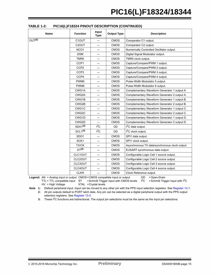
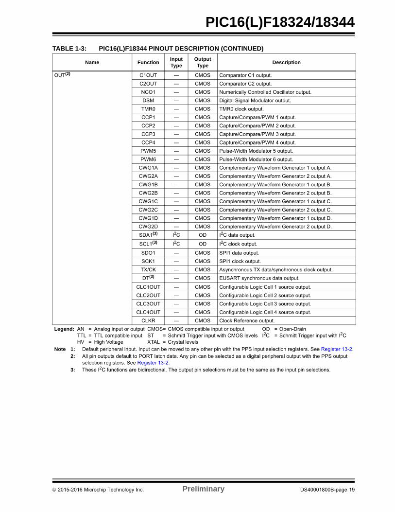
OUT(2) C1OUT ― CMOS Comparator C1 output.
C2OUT ― CMOS Comparator C2 output.
NCO1 ― CMOS Numerically Controlled Oscillator output.
DSM ― CMOS Digital Signal Modulator output.
TMR0 ― CMOS TMR0 clock output.
CCP1 ― CMOS Capture/Compare/PWM 1 output.
CCP2 ― CMOS Capture/Compare/PWM 2 output.
CCP3 ― CMOS Capture/Compare/PWM 3 output.
CCP4 ― CMOS Capture/Compare/PWM 4 output.
PWM5 ― CMOS Pulse-Width Modulator 5 output.
PWM6 ― CMOS Pulse-Width Modulator 6 output.
CWG1A ― CMOS Complementary Waveform Generator 1 output A.
CWG2A ― CMOS Complementary Waveform Generator 2 output A.
CWG1B ― CMOS Complementary Waveform Generator 1 output B.
CWG2B ― CMOS Complementary Waveform Generator 2 output B.
CWG1C ― CMOS Complementary Waveform Generator 1 output C.
CWG2C ― CMOS Complementary Waveform Generator 2 output C.
CWG1D ― CMOS Complementary Waveform Generator 1 output D.
CWG2D ― CMOS Complementary Waveform Generator 2 output D.
SDA1(3) I2C OD I2C data output.
SCL1(3) I2C OD I2C clock output.
SDO1 ― CMOS SPI1 data output.
SCK1 ― CMOS SPI1 clock output.
TX/CK ― CMOS Asynchronous TX data/synchronous clock output.
DT(3) ― CMOS EUSART synchronous data output.
CLC1OUT ― CMOS Configurable Logic Cell 1 source output.
CLC2OUT ― CMOS Configurable Logic Cell 2 source output.
CLC3OUT ― CMOS Configurable Logic Cell 3 source output.
CLC4OUT ― CMOS Configurable Logic Cell 4 source output.
CLKR ― CMOS Clock Reference output.
TABLE 1-2: PIC16(L)F18324 PINOUT DESCRIPTION (CONTINUED)
Name FunctionInput Type
Output Type Description
Legend: AN = Analog input or output CMOS=CMOS compatible input or output OD = Open-DrainTTL = TTL compatible input ST =Schmitt Trigger input with CMOS levels I2C = Schmitt Trigger input with I2C HV = High Voltage XTAL =Crystal levels
Note 1: Default peripheral input. Input can be moved to any other pin with the PPS input selection registers. See Register 13-1.2: All pin outputs default to PORT latch data. Any pin can be selected as a digital peripheral output with the PPS output
selection registers. See Register 13-2.3: These I2C functions are bidirectional. The output pin selections must be the same as the input pin selections.
2015-2016 Microchip Technology Inc. Preliminary DS40001800B-page 15
PIC16(L)F18324/18344
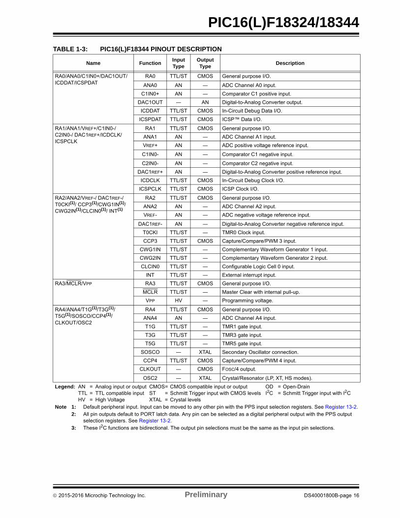
TABLE 1-3: PIC16(L)F18344 PINOUT DESCRIPTION
Name FunctionInput Type
Output Type
Description
RA0/ANA0/C1IN0+/DAC1OUT/ ICDDAT/ICSPDAT
RA0 TTL/ST CMOS General purpose I/O.
ANA0 AN ― ADC Channel A0 input.
C1IN0+ AN ― Comparator C1 positive input.
DAC1OUT ― AN Digital-to-Analog Converter output.
ICDDAT TTL/ST CMOS In-Circuit Debug Data I/O.
ICSPDAT TTL/ST CMOS ICSP™ Data I/O.
RA1/ANA1/VREF+/C1IN0-/C2IN0-/ DAC1REF+/ICDCLK/ ICSPCLK
RA1 TTL/ST CMOS General purpose I/O.
ANA1 AN ― ADC Channel A1 input.
VREF+ AN ― ADC positive voltage reference input.
C1IN0- AN ― Comparator C1 negative input.
C2IN0- AN ― Comparator C2 negative input.
DAC1REF+ AN ― Digital-to-Analog Converter positive reference input.
ICDCLK TTL/ST CMOS In-Circuit Debug Clock I/O.
ICSPCLK TTL/ST CMOS ICSP Clock I/O.
RA2/ANA2/VREF-/ DAC1REF-/T0CKI(1)/ CCP3(1)/CWG1IN(1)/ CWG2IN(1)/CLCIN0(1)/ INT(1)
RA2 TTL/ST CMOS General purpose I/O.
ANA2 AN ― ADC Channel A2 input.
VREF- AN ― ADC negative voltage reference input.
DAC1REF- AN ― Digital-to-Analog Converter negative reference input.
T0CKI TTL/ST ― TMR0 Clock input.
CCP3 TTL/ST CMOS Capture/Compare/PWM 3 input.
CWG1IN TTL/ST ― Complementary Waveform Generator 1 input.
CWG2IN TTL/ST ― Complementary Waveform Generator 2 input.
CLCIN0 TTL/ST ― Configurable Logic Cell 0 input.
INT TTL/ST ― External interrupt input.
RA3/MCLR/VPP RA3 TTL/ST CMOS General purpose I/O.
MCLR TTL/ST ― Master Clear with internal pull-up.
VPP HV ― Programming voltage.
RA4/ANA4/T1G(1)/T3G(1)/T5G(1)/SOSCO/CCP4(1)/ CLKOUT/OSC2
RA4 TTL/ST CMOS General purpose I/O.
ANA4 AN ― ADC Channel A4 input.
T1G TTL/ST ― TMR1 gate input.
T3G TTL/ST ― TMR3 gate input.
T5G TTL/ST ― TMR5 gate input.
SOSCO ― XTAL Secondary Oscillator connection.
CCP4 TTL/ST CMOS Capture/Compare/PWM 4 input.
CLKOUT ― CMOS FOSC/4 output.
OSC2 ― XTAL Crystal/Resonator (LP, XT, HS modes).
Legend: AN = Analog input or output CMOS= CMOS compatible input or output OD = Open-DrainTTL = TTL compatible input ST = Schmitt Trigger input with CMOS levels I2C = Schmitt Trigger input with I2CHV = High Voltage XTAL = Crystal levels
Note 1: Default peripheral input. Input can be moved to any other pin with the PPS input selection registers. See Register 13-2.2: All pin outputs default to PORT latch data. Any pin can be selected as a digital peripheral output with the PPS output
selection registers. See Register 13-2.3: These I2C functions are bidirectional. The output pin selections must be the same as the input pin selections.
2015-2016 Microchip Technology Inc. Preliminary DS40001800B-page 16
PIC16(L)F18324/18344
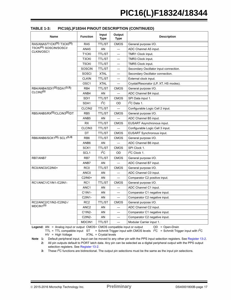
RA5/ANA5/T1CKI(1)/ T3CKI(1)/T5CKI(1)/ SOSCIN/SOSCI/ CLKIN/OSC1
RA5 TTL/ST CMOS General purpose I/O.
ANA5 AN ― ADC Channel A5 input.
T1CKI TTL/ST ― TMR1 Clock input.
T3CKI TTL/ST ― TMR3 Clock input.
T5CKI TTL/ST ― TMR5 Clock input.
SOSCIN TTL/ST ― Secondary Oscillator input connection.
SOSCI XTAL ― Secondary Oscillator connection.
CLKIN TTL/ST ― External clock input.
OSC1 XTAL ― Crystal/Resonator (LP, XT, HS modes).
RB4/ANB4/SDI1(1)/SDA1(1,3)/CLCIN2(1)
RB4 TTL/ST CMOS General purpose I/O.
ANB4 AN ― ADC Channel B4 input.
SDI1 TTL/ST CMOS SPI Data input 1.
SDA1 I2C OD I2C Data 1.
CLCIN2 TTL/ST ― Configurable Logic Cell 2 input.
RB5/ANB5/RX(1)/CLCIN3(1)/DT RB5 TTL/ST CMOS General purpose I/O.
ANB5 AN ― ADC Channel B5 input.
RX TTL/ST CMOS EUSART Asynchronous input.
CLCIN3 TTL/ST ― Configurable Logic Cell 3 input.
DT TTL/ST CMOS EUSART Synchronous input.
RB6/ANB6/SCK1(1)/ SCL1(1,3) RB6 TTL/ST CMOS General purpose I/O.
ANB6 AN ― ADC Channel B6 input.
SCK1 TTL/ST CMOS SPI Clock 1.
SCL1 I2C OD I2C Clock 1.
RB7/ANB7 RB7 TTL/ST CMOS General purpose I/O.
ANB7 AN ― ADC Channel B7 input.
RC0/ANC0/C2IN0+ RC0 TTL/ST CMOS General purpose I/O.
ANC0 AN ― ADC Channel C0 input.
C2IN0+ AN ― Comparator C2 positive input.
RC1/ANC1/C1IN1-/C2IN1- RC1 TTL/ST CMOS General purpose I/O.
ANC1 AN ― ADC Channel C1 input.
C1IN1- AN ― Comparator C1 negative input.
C2IN1- AN ― Comparator C2 negative input.
RC2/ANC2/C1IN2-/C2IN2-/MDCIN1(1)
RC2 TTL/ST CMOS General purpose I/O.
ANC2 AN ― ADC Channel C2 input.
C1IN2- AN ― Comparator C1 negative input.
C2IN2- AN ― Comparator C2 negative input.
MDCIN1 TTL/ST ― Modular Carrier input 1.
TABLE 1-3: PIC16(L)F18344 PINOUT DESCRIPTION (CONTINUED)
Name FunctionInput Type
Output Type
Description
Legend: AN = Analog input or output CMOS= CMOS compatible input or output OD = Open-DrainTTL = TTL compatible input ST = Schmitt Trigger input with CMOS levels I2C = Schmitt Trigger input with I2CHV = High Voltage XTAL = Crystal levels
Note 1: Default peripheral input. Input can be moved to any other pin with the PPS input selection registers. See Register 13-2.2: All pin outputs default to PORT latch data. Any pin can be selected as a digital peripheral output with the PPS output
selection registers. See Register 13-2.3: These I2C functions are bidirectional. The output pin selections must be the same as the input pin selections.
2015-2016 Microchip Technology Inc. Preliminary DS40001800B-page 17
PIC16(L)F18324/18344
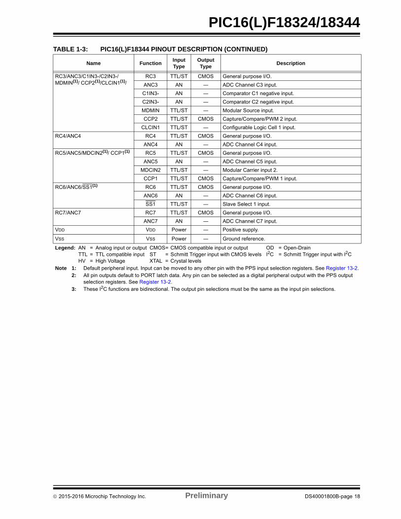
RC3/ANC3/C1IN3-/C2IN3-/MDMIN(1)/ CCP2(1)/CLCIN1(1)/
RC3 TTL/ST CMOS General purpose I/O.
ANC3 AN ― ADC Channel C3 input.
C1IN3- AN ― Comparator C1 negative input.
C2IN3- AN ― Comparator C2 negative input.
MDMIN TTL/ST ― Modular Source input.
CCP2 TTL/ST CMOS Capture/Compare/PWM 2 input.
CLCIN1 TTL/ST ― Configurable Logic Cell 1 input.
RC4/ANC4 RC4 TTL/ST CMOS General purpose I/O.
ANC4 AN ― ADC Channel C4 input.
RC5/ANC5/MDCIN2(1)/ CCP1(1) RC5 TTL/ST CMOS General purpose I/O.
ANC5 AN ― ADC Channel C5 input.
MDCIN2 TTL/ST ― Modular Carrier input 2.
CCP1 TTL/ST CMOS Capture/Compare/PWM 1 input.
RC6/ANC6/SS1(1) RC6 TTL/ST CMOS General purpose I/O.
ANC6 AN ― ADC Channel C6 input.
SS1 TTL/ST ― Slave Select 1 input.
RC7/ANC7 RC7 TTL/ST CMOS General purpose I/O.
ANC7 AN ― ADC Channel C7 input.
VDD VDD Power ― Positive supply.
VSS VSS Power ― Ground reference.
TABLE 1-3: PIC16(L)F18344 PINOUT DESCRIPTION (CONTINUED)
Name FunctionInput Type
Output Type
Description
Legend: AN = Analog input or output CMOS= CMOS compatible input or output OD = Open-DrainTTL = TTL compatible input ST = Schmitt Trigger input with CMOS levels I2C = Schmitt Trigger input with I2CHV = High Voltage XTAL = Crystal levels
Note 1: Default peripheral input. Input can be moved to any other pin with the PPS input selection registers. See Register 13-2.2: All pin outputs default to PORT latch data. Any pin can be selected as a digital peripheral output with the PPS output
selection registers. See Register 13-2.3: These I2C functions are bidirectional. The output pin selections must be the same as the input pin selections.
2015-2016 Microchip Technology Inc. Preliminary DS40001800B-page 18
PIC16(L)F18324/18344
OUT(2) C1OUT ― CMOS Comparator C1 output.
C2OUT ― CMOS Comparator C2 output.
NCO1 ― CMOS Numerically Controlled Oscillator output.
DSM ― CMOS Digital Signal Modulator output.
TMR0 ― CMOS TMR0 clock output.
CCP1 ― CMOS Capture/Compare/PWM 1 output.
CCP2 ― CMOS Capture/Compare/PWM 2 output.
CCP3 ― CMOS Capture/Compare/PWM 3 output.
CCP4 ― CMOS Capture/Compare/PWM 4 output.
PWM5 ― CMOS Pulse-Width Modulator 5 output.
PWM6 ― CMOS Pulse-Width Modulator 6 output.
CWG1A ― CMOS Complementary Waveform Generator 1 output A.
CWG2A ― CMOS Complementary Waveform Generator 2 output A.
CWG1B ― CMOS Complementary Waveform Generator 1 output B.
CWG2B ― CMOS Complementary Waveform Generator 2 output B.
CWG1C ― CMOS Complementary Waveform Generator 1 output C.
CWG2C ― CMOS Complementary Waveform Generator 2 output C.
CWG1D ― CMOS Complementary Waveform Generator 1 output D.
CWG2D ― CMOS Complementary Waveform Generator 2 output D.
SDA1(3) I2C OD I2C data output.
SCL1(3) I2C OD I2C clock output.
SDO1 ― CMOS SPI1 data output.
SCK1 ― CMOS SPI1 clock output.
TX/CK ― CMOS Asynchronous TX data/synchronous clock output.
DT(3) ― CMOS EUSART synchronous data output.
CLC1OUT ― CMOS Configurable Logic Cell 1 source output.
CLC2OUT ― CMOS Configurable Logic Cell 2 source output.
CLC3OUT ― CMOS Configurable Logic Cell 3 source output.
CLC4OUT ― CMOS Configurable Logic Cell 4 source output.
CLKR ― CMOS Clock Reference output.
TABLE 1-3: PIC16(L)F18344 PINOUT DESCRIPTION (CONTINUED)
Name FunctionInput Type
Output Type
Description
Legend: AN = Analog input or output CMOS= CMOS compatible input or output OD = Open-DrainTTL = TTL compatible input ST = Schmitt Trigger input with CMOS levels I2C = Schmitt Trigger input with I2CHV = High Voltage XTAL = Crystal levels
Note 1: Default peripheral input. Input can be moved to any other pin with the PPS input selection registers. See Register 13-2.2: All pin outputs default to PORT latch data. Any pin can be selected as a digital peripheral output with the PPS output
selection registers. See Register 13-2.3: These I2C functions are bidirectional. The output pin selections must be the same as the input pin selections.
2015-2016 Microchip Technology Inc. Preliminary DS40001800B-page 19
PIC16(L)F18324/18344
2.0 GUIDELINES FOR GETTING STARTED WITH PIC16(L)F183XX MICROCONTROLLERS
2.1 Basic Connection Requirements
Getting started with the PIC16(L)F183XX family of 8-bitmicrocontrollers requires attention to a minimal set ofdevice pin connections before proceeding withdevelopment.
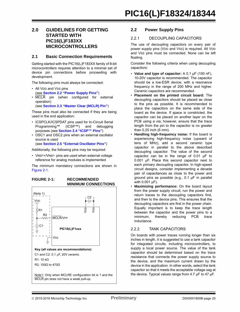
The following pins must always be connected:
• All VDD and VSS pins(see Section 2.2 “Power Supply Pins”)
• MCLR pin (when configured for externaloperation)(see Section 2.3 “Master Clear (MCLR) Pin”)
These pins must also be connected if they are beingused in the end application:
• ICSPCLK/ICSPDAT pins used for In-Circuit SerialProgramming™ (ICSP™) and debuggingpurposes (see Section 2.4 “ICSP™ Pins”)
• OSC1 and OSC2 pins when an external oscillatorsource is used(see Section 2.5 “External Oscillator Pins”)
Additionally, the following pins may be required:
• VREF+/VREF- pins are used when external voltage reference for analog modules is implemented
The minimum mandatory connections are shown inFigure 2-1.
FIGURE 2-1: RECOMMENDED MINIMUM CONNECTIONS
2.2 Power Supply Pins
2.2.1 DECOUPLING CAPACITORS
The use of decoupling capacitors on every pair ofpower supply pins (VDD and VSS) is required. All VDD
and VSS pins must be connected. None can be leftfloating.
Consider the following criteria when using decouplingcapacitors:
• Value and type of capacitor: A 0.1 µF (100 nF),10-20V capacitor is recommended. The capacitorshould be a low-ESR device, with a resonancefrequency in the range of 200 MHz and higher.Ceramic capacitors are recommended.
• Placement on the printed circuit board: Thedecoupling capacitors should be placed as closeto the pins as possible. It is recommended toplace the capacitors on the same side of theboard as the device. If space is constricted, thecapacitor can be placed on another layer on thePCB using a via; however, ensure that the tracelength from the pin to the capacitor is no greaterthan 0.25 inch (6 mm).
• Handling high-frequency noise: If the board isexperiencing high-frequency noise (upward oftens of MHz), add a second ceramic typecapacitor in parallel to the above describeddecoupling capacitor. The value of the secondcapacitor can be in the range of 0.01 µF to0.001 µF. Place this second capacitor next toeach primary decoupling capacitor. In high-speedcircuit designs, consider implementing a decadepair of capacitances as close to the power andground pins as possible (e.g., 0.1 µF in parallelwith 0.001 µF).
• Maximizing performance: On the board layoutfrom the power supply circuit, run the power andreturn traces to the decoupling capacitors first,and then to the device pins. This ensures that thedecoupling capacitors are first in the power chain.Equally important is to keep the trace lengthbetween the capacitor and the power pins to aminimum, thereby reducing PCB traceinductance.
2.2.2 TANK CAPACITORS
On boards with power traces running longer than sixinches in length, it is suggested to use a tank capacitorfor integrated circuits, including microcontrollers, tosupply a local power source. The value of the tankcapacitor should be determined based on the traceresistance that connects the power supply source tothe device, and the maximum current drawn by thedevice in the application. In other words, select the tankcapacitor so that it meets the acceptable voltage sag atthe device. Typical values range from 4.7 µF to 47 µF.
VD
D
VS
S
VSS
C1
R1
VDD
MCLR/VPPR2
C2
Key (all values are recommendations):C1 and C2: 0.1 F, 20V ceramicR1: 10 kR2: 100 to 470
Note1: Only when MCLRE configuration bit is 1 and theMCLR pin does not have a weak pull-up.
PIC16(L)F1xxx
(Note 1)
2015-2016 Microchip Technology Inc. Preliminary DS40001800B-page 20
PIC16(L)F18324/18344
2.3 Master Clear (MCLR) Pin
The MCLR pin provides three specific device functions:
• Device Reset (when MCLRE = 1)• Digital input pin (when MCLRE = 0)• Device Programming and Debugging
If programming and debugging are not required in theend application then either set the MCLREconfiguration bit to ‘1’ and use the pin as a digital inputor clear the MCLRE Configuration bit and leave the pinopen to use the internal weak pull-up. The addition ofother components, to help increase the application’sresistance to spurious Resets from voltage sags, maybe beneficial. A typical configuration is shown inFigure 2-1. Other circuit designs may be implemented,depending on the application’s requirements.
During programming and debugging, the resistanceand capacitance that can be added to the pin must beconsidered. Device programmers and debuggers drivethe MCLR pin. Consequently, specific voltage levels(VIH and VIL) and fast signal transitions must not beadversely affected. Therefore, the programmerMCLR/VPP output should be connected directly to thepin so that R1 isolates the capacitor, C1 from the MCLRpin during programming and debugging operations.
Any components associated with the MCLR pin shouldbe placed within 0.25 inch (6 mm) of the pin.
2.4 ICSP™ Pins
The ICSPCLK and ICSPDAT pins are used forIn-Circuit Serial Programming™ (ICSP™) anddebugging purposes. It is recommended to keep thetrace length between the ICSP connector and the ICSPpins on the device as short as possible. If the ICSPconnector is expected to experience an ESD event, aseries resistor is recommended, with the value in therange of a few tens of ohms, not to exceed 100Ω.
Pull-up resistors, series diodes and capacitors on theICSPCLK and ICSPDAT pins are not recommended asthey will interfere with the programmer/debuggercommunications to the device. If such discretecomponents are an application requirement, theyshould be isolated from the programmer by resistorsbetween the application and the device pins orremoved from the circuit during programming.Alternatively, refer to the AC/DC characteristics andtiming requirements information in the respectivedevice Flash programming specification for informationon capacitive loading limits, and pin input voltage high(VIH) and input low (VIL) requirements.
For device emulation, ensure that the “CommunicationChannel Select” (i.e., ICSPCLK/ICSPDAT pins),programmed into the device, matches the physicalconnections for the ICSP to the Microchip debugger/emulator tool.
For more information on available Microchipdevelopment tools connection requirements, refer toSection 37.0 “Development Support”.
2015-2016 Microchip Technology Inc. Preliminary DS40001800B-page 21
PIC16(L)F18324/18344
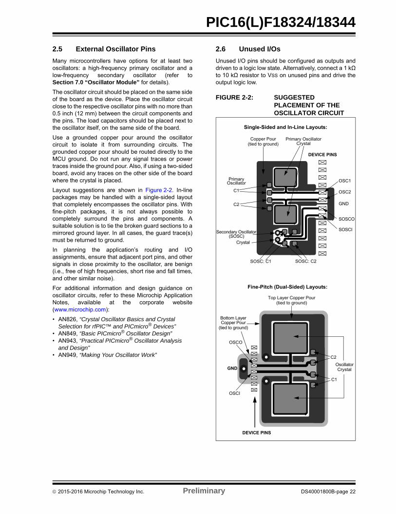
2.5 External Oscillator Pins
Many microcontrollers have options for at least twooscillators: a high-frequency primary oscillator and alow-frequency secondary oscillator (refer toSection 7.0 “Oscillator Module” for details).
The oscillator circuit should be placed on the same sideof the board as the device. Place the oscillator circuitclose to the respective oscillator pins with no more than0.5 inch (12 mm) between the circuit components andthe pins. The load capacitors should be placed next tothe oscillator itself, on the same side of the board.
Use a grounded copper pour around the oscillatorcircuit to isolate it from surrounding circuits. Thegrounded copper pour should be routed directly to theMCU ground. Do not run any signal traces or powertraces inside the ground pour. Also, if using a two-sidedboard, avoid any traces on the other side of the boardwhere the crystal is placed.
Layout suggestions are shown in Figure 2-2. In-linepackages may be handled with a single-sided layoutthat completely encompasses the oscillator pins. Withfine-pitch packages, it is not always possible tocompletely surround the pins and components. Asuitable solution is to tie the broken guard sections to amirrored ground layer. In all cases, the guard trace(s)must be returned to ground.
In planning the application’s routing and I/Oassignments, ensure that adjacent port pins, and othersignals in close proximity to the oscillator, are benign(i.e., free of high frequencies, short rise and fall times,and other similar noise).
For additional information and design guidance onoscillator circuits, refer to these Microchip ApplicationNotes, available at the corporate website(www.microchip.com):
• AN826, “Crystal Oscillator Basics and Crystal Selection for rfPIC™ and PICmicro® Devices”
• AN849, “Basic PICmicro® Oscillator Design”• AN943, “Practical PICmicro® Oscillator Analysis
and Design”• AN949, “Making Your Oscillator Work”
2.6 Unused I/Os
Unused I/O pins should be configured as outputs anddriven to a logic low state. Alternatively, connect a 1 kΩto 10 kΩ resistor to VSS on unused pins and drive theoutput logic low.
FIGURE 2-2: SUGGESTED PLACEMENT OF THE OSCILLATOR CIRCUIT
GND
`
`
`
OSC1
OSC2
SOSCO
SOSCI
Copper Pour Primary OscillatorCrystal
Secondary Oscillator
Crystal
DEVICE PINS
PrimaryOscillator
C1
C2
SOSC: C1 SOSC: C2
(tied to ground)
Single-Sided and In-Line Layouts:
Fine-Pitch (Dual-Sided) Layouts:
GND
OSCO
OSCI
Bottom LayerCopper Pour
OscillatorCrystal
Top Layer Copper Pour
C2
C1
DEVICE PINS
(tied to ground)
(tied to ground)
(SOSC)
2015-2016 Microchip Technology Inc. Preliminary DS40001800B-page 22
PIC16(L)F18324/18344
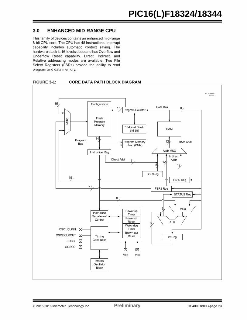
3.0 ENHANCED MID-RANGE CPU
This family of devices contains an enhanced mid-range8-bit CPU core. The CPU has 48 instructions. Interruptcapability includes automatic context saving. Thehardware stack is 16-levels deep and has Overflow andUnderflow Reset capability. Direct, Indirect, andRelative addressing modes are available. Two FileSelect Registers (FSRs) provide the ability to readprogram and data memory.
FIGURE 3-1: CORE DATA PATH BLOCK DIAGRAM
Rev. 10-000055B8/23/2016
1515
15
15
8
8
8
1214
75
3
Program Counter
MUX
Addr MUX
16-Level Stack (15-bit)
Program Memory Read (PMR)
Instruction Reg
Configuration
FSR0 Reg
FSR1 Reg
BSR Reg
STATUS Reg
RAM
W Reg
Power-upTimer
Power-on Reset
Watchdog Timer
Brown-out Reset
Instruction Decode and
Control
Timing Generation
Internal Oscillator
Block
ALU
Flash Program MemoryM
UX
Data Bus
Program Bus
Direct AddrIndirect
Addr
RAM Addr
OSC1/CLKIN
OSC2/CLKOUT
VDD VSS
1212
SOSCI
SOSCO
2015-2016 Microchip Technology Inc. Preliminary DS40001800B-page 23
PIC16(L)F18324/18344
3.1 Automatic Interrupt Context Saving
During interrupts, certain registers are automaticallysaved in shadow registers and restored when returningfrom the interrupt. This saves stack space and usercode. See Section 8.5 “Automatic Context Saving”for more information.
3.2 16-Level Stack with Overflow and Underflow
These devices have a hardware stack memory 15-bitswide and 16-words deep. A Stack Overflow orUnderflow will set the appropriate bit (STKOVF orSTKUNF) in the PCON register, and if enabled, willcause a software Reset. See Section 4.4 “Stack” formore details.
3.3 File Select Registers
There are two 16-bit File Select Registers (FSR). FSRscan access all file registers, program memory and dataEEPROM, which allows one Data Pointer for all mem-ory. When an FSR points to program memory, there isone additional instruction cycle in instructions usingINDF to allow the data to be fetched. General purposememory can now also be addressed linearly, providingthe ability to access contiguous data larger than 80bytes. See Section 4.5 “Indirect Addressing” formore details.
3.4 Instruction Set
There are 48 instructions for the enhanced mid-rangeCPU to support the features of the CPU. SeeSection 34.0 “Instruction Set Summary” for moredetails.
2015-2016 Microchip Technology Inc. Preliminary DS40001800B-page 24
PIC16(L)F18324/18344
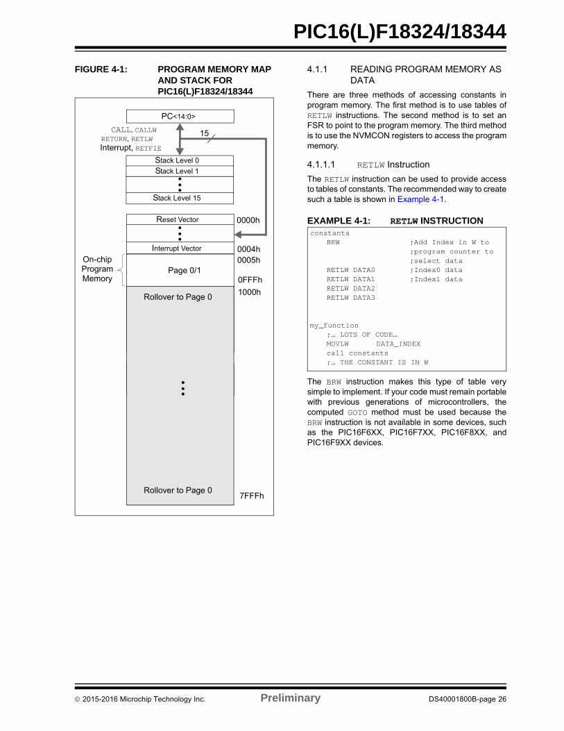
4.0 MEMORY ORGANIZATION
These devices contain the following types of memory:
• Program Memory- Configuration Words- Device ID- Revision ID- User ID- Program Flash Memory
• Data Memory- Core Registers- Special Function Registers- General Purpose RAM- Common RAM
• Data EEPROM
4.1 Program Memory Organization
The enhanced mid-range core has a 15-bit programcounter capable of addressing 32K x 14 programmemory space. Table 4-1 shows the memory sizesimplemented. Accessing a location above theseboundaries will cause a wrap-around within theimplemented memory space. The Reset vector is at0000h and the interrupt vector is at 0004h (seeFigure 4-1).
TABLE 4-1: DEVICE SIZES AND ADDRESSES
Device Program Memory Size (Words) Last Program Memory Address
PIC16(L)F18324/18344 4096 0FFFh
2015-2016 Microchip Technology Inc. Preliminary DS40001800B-page 25
PIC16(L)F18324/18344
FIGURE 4-1: PROGRAM MEMORY MAP AND STACK FOR PIC16(L)F18324/18344
4.1.1 READING PROGRAM MEMORY AS DATA
There are three methods of accessing constants inprogram memory. The first method is to use tables ofRETLW instructions. The second method is to set anFSR to point to the program memory. The third methodis to use the NVMCON registers to access the programmemory.
4.1.1.1 RETLW Instruction
The RETLW instruction can be used to provide accessto tables of constants. The recommended way to createsuch a table is shown in Example 4-1.
EXAMPLE 4-1: RETLW INSTRUCTION
The BRW instruction makes this type of table verysimple to implement. If your code must remain portablewith previous generations of microcontrollers, thecomputed GOTO method must be used because theBRW instruction is not available in some devices, suchas the PIC16F6XX, PIC16F7XX, PIC16F8XX, andPIC16F9XX devices.
PC<14:0>
15
0000h
0004h
Stack Level 0
Stack Level 15
Reset Vector
Interrupt Vector
Stack Level 1
0005hOn-chipProgramMemory
Page 0/10FFFh
Wraps to Page 0
Wraps to Page 0
Wraps to Page 0
1000h
CALL, CALLW RETURN, RETLW
Interrupt, RETFIE
Rollover to Page 0
Rollover to Page 07FFFh
constantsBRW ;Add Index in W to
;program counter to;select data
RETLW DATA0 ;Index0 dataRETLW DATA1 ;Index1 dataRETLW DATA2RETLW DATA3
my_function;… LOTS OF CODE…MOVLW DATA_INDEXcall constants;… THE CONSTANT IS IN W
2015-2016 Microchip Technology Inc. Preliminary DS40001800B-page 26
PIC16(L)F18324/18344
4.1.1.2 Indirect Read with FSR
The program memory can be accessed as data bysetting bit 7 of an FSRxH register and reading thematching INDFx register. The MOVIW instruction willplace the lower eight bits of the addressed word in theW register. Writes to the program memory cannot beperformed via the INDF registers. Instructions that readthe program memory via the FSR require one extrainstruction cycle to complete. Example 4-2demonstrates reading the program memory via anFSR.
The HIGH directive will set bit 7 if a label points to alocation in the program memory.
EXAMPLE 4-2: ACCESSING PROGRAM MEMORY VIA FSR
4.1.1.3 NVMREG Access
The NVMREG interface allows read/write access to alllocations accessible by the FSRs, User ID locations,and EEPROM. The NVMREG interface also providesread-only access to Device ID, Revision ID, andConfiguration data. See Section 11.4 “NVMREGAccess” for more information.
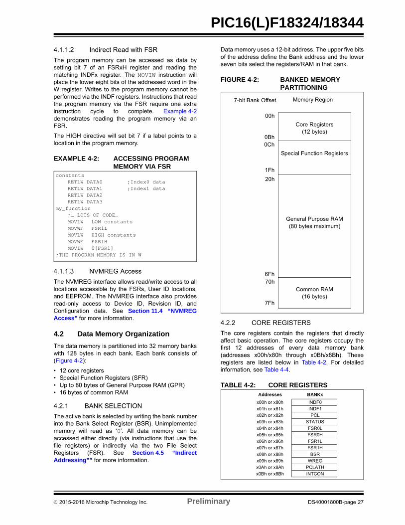
4.2 Data Memory Organization
The data memory is partitioned into 32 memory bankswith 128 bytes in each bank. Each bank consists of(Figure 4-2):
• 12 core registers• Special Function Registers (SFR)• Up to 80 bytes of General Purpose RAM (GPR) • 16 bytes of common RAM
4.2.1 BANK SELECTION
The active bank is selected by writing the bank numberinto the Bank Select Register (BSR). Unimplementedmemory will read as ‘0’. All data memory can beaccessed either directly (via instructions that use thefile registers) or indirectly via the two File SelectRegisters (FSR). See Section 4.5 “IndirectAddressing”” for more information.
Data memory uses a 12-bit address. The upper five bitsof the address define the Bank address and the lowerseven bits select the registers/RAM in that bank.
FIGURE 4-2: BANKED MEMORY PARTITIONING
4.2.2 CORE REGISTERS
The core registers contain the registers that directlyaffect basic operation. The core registers occupy thefirst 12 addresses of every data memory bank(addresses x00h/x80h through x0Bh/x8Bh). Theseregisters are listed below in Table 4-2. For detailedinformation, see Table 4-4.
TABLE 4-2: CORE REGISTERS
constantsRETLW DATA0 ;Index0 dataRETLW DATA1 ;Index1 dataRETLW DATA2RETLW DATA3
my_function;… LOTS OF CODE…MOVLW LOW constantsMOVWF FSR1LMOVLW HIGH constantsMOVWF FSR1HMOVIW 0[FSR1]
;THE PROGRAM MEMORY IS IN W
0Bh0Ch
1Fh
20h
6Fh70h
7Fh
00h
Common RAM(16 bytes)
General Purpose RAM(80 bytes maximum)
Core Registers(12 bytes)
Special Function Registers
Memory Region7-bit Bank Offset
Addresses BANKx
x00h or x80h INDF0
x01h or x81h INDF1
x02h or x82h PCL
x03h or x83h STATUS
x04h or x84h FSR0L
x05h or x85h FSR0H
x06h or x86h FSR1L
x07h or x87h FSR1H
x08h or x88h BSR
x09h or x89h WREG
x0Ah or x8Ah PCLATH
x0Bh or x8Bh INTCON
2015-2016 Microchip Technology Inc. Preliminary DS40001800B-page 27
PIC16(L)F18324/18344
4.2.2.1 STATUS Register
The STATUS register, shown in Register 4-1, contains:
• The arithmetic status of the ALU
• The Reset status
The STATUS register can be the destination for anyinstruction, like any other register. If the STATUSregister is the destination for an instruction that affectsthe Z, DC or C bits, then the write to these three bits isdisabled. These bits are set or cleared according to thedevice logic. Furthermore, the TO and PD bits are notwritable. Therefore, the result of an instruction with theSTATUS register as destination may be different thanintended.
For example, CLRF STATUS will clear the upper threebits and set the Z bit. This leaves the STATUS registeras ‘000u u1uu’ (where u = unchanged).
It is recommended, therefore, that only BCF, BSF,SWAPF and MOVWF instructions are used to alter theSTATUS register, because these instructions do notaffect any Status bits. For other instructions notaffecting any Status bits (Refer to Section 34.0“Instruction Set Summary”).
Note 1: The C and DC bits operate as Borrowand Digit Borrow out bits, respectively, insubtraction.
REGISTER 4-1: STATUS: STATUS REGISTER
U-0 U-0 U-0 R-1/q R-1/q R/W-0/u R/W-0/u R/W-0/u
— — — TO PD Z DC(1) C(1)
bit 7 bit 0
Legend:
R = Readable bit W = Writable bit U = Unimplemented bit, read as ‘0’
u = Bit is unchanged x = Bit is unknown -n/n = Value at POR and BOR/Value at all other Resets
‘1’ = Bit is set ‘0’ = Bit is cleared q = Value depends on condition
bit 7-5 Unimplemented: Read as ‘0’
bit 4 TO: Time-Out bit
1 = After power-up, CLRWDT instruction or SLEEP instruction0 = A WDT time-out occurred
bit 3 PD: Power-Down bit
1 = After power-up or by the CLRWDT instruction0 = By execution of the SLEEP instruction
bit 2 Z: Zero bit
1 = The result of an arithmetic or logic operation is zero0 = The result of an arithmetic or logic operation is not zero
bit 1 DC: Digit Carry/Digit Borrow bit (ADDWF, ADDLW, SUBLW, SUBWF instructions)(1)
1 = A carry-out from the 4th low-order bit of the result occurred0 = No carry-out from the 4th low-order bit of the result
bit 0 C: Carry/Borrow bit(1) (ADDWF, ADDLW, SUBLW, SUBWF instructions)(1)
1 = A carry-out from the Most Significant bit of the result occurred0 = No carry-out from the Most Significant bit of the result occurred
Note 1: For Borrow, the polarity is reversed. A subtraction is executed by adding the two’s complement of the second operand. For rotate (RRF, RLF) instructions, this bit is loaded with either the high-order or low-order bit of the source register.
2015-2016 Microchip Technology Inc. Preliminary DS40001800B-page 28
PIC16(L)F18324/18344
4.2.3 SPECIAL FUNCTION REGISTERS
The Special Function Registers are registers used bythe application to control the desired operation ofperipheral functions in the device. The Special FunctionRegisters occupy the 20 bytes after the core registers ofevery data memory bank (addresses x0Ch/x8Chthrough x1Fh/x9Fh), with the exception of banks 27, 28and 29 (PPS and CLC registers). The registersassociated with the operation of the peripherals aredescribed in the appropriate peripheral chapter of thisdata sheet.
4.2.4 GENERAL PURPOSE RAM
There are up to 80 bytes of GPR in each data memorybank. The general purpose RAM can be accessed in anon-banked method via the FSRs. This can simplifyaccess to large memory structures. See Section 4.5.2“Linear Data Memory” for more information.
4.2.5 COMMON RAM
There are 16 bytes of common RAM accessible from allbanks.
4.2.6 DEVICE MEMORY MAPS
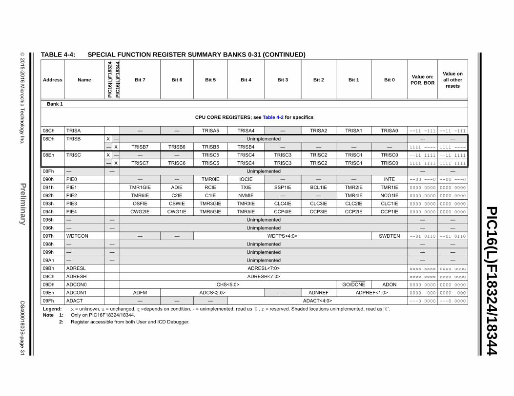
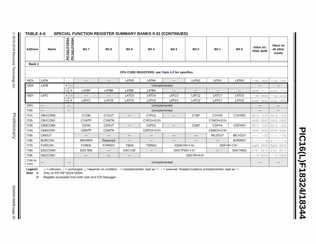
The memory maps for PIC16(L)F18324/18344 are asshown in Table 4-4.
TABLE 4-3: SPECIAL FUNCTION REGISTER SUMMARY BANKS 0-31 (ALL BANKS)(1)
Bank Offset
Name Bit 7 Bit 6 Bit 5 Bit 4 Bit 3 Bit 2 Bit 1 Bit 0Value on:POR, BOR
Value on all other
Resets
All Banks
000h INDF0 Addressing this location uses contents of FSR0H/FSR0L to address data memory (not a physical register)
xxxx xxxx xxxx xxxx
001h INDF1 Addressing this location uses contents of FSR1H/FSR1L to address data memory (not a physical register)
xxxx xxxx xxxx xxxx
002h PCL Program Counter (PC) Least Significant Byte 0000 0000 0000 0000
003h STATUS — — — TO PD Z DC C ---1 1000 ---q quuu
004h FSR0L Indirect Data Memory Address 0 Low Pointer 0000 0000 uuuu uuuu
005h FSR0H Indirect Data Memory Address 0 High Pointer 0000 0000 0000 0000
006h FSR1L Indirect Data Memory Address 1 Low Pointer 0000 0000 uuuu uuuu
007h FSR1H Indirect Data Memory Address 1 High Pointer 0000 0000 0000 0000
008h BSR — — — BSR4 BSR3 BSR2 BSR1 BSR0 ---0 0000 ---0 0000
009h WREG Working Register 0000 0000 uuuu uuuu
00Ah PCLATH — Write Buffer for the upper 7 bits of the Program Counter -000 0000 -000 0000
00Bh INTCON GIE PEIE — — — — — INTEDG 00-- ---1 00-- ---1
Legend: x = unknown, u = unchanged, q =depends on condition, - = unimplemented, read as ‘0’, r = reserved. Shaded locations unimplemented, read as ‘0’.
Note 1: These Registers can be accessed from any bank.
2015-2016 Microchip Technology Inc. Preliminary DS40001800B-page 29
2
01
5-2
01
6 M
icroch
ip T
ech
no
log
y Inc.
Prelim
inary
DS
40
00
18
00
B-p
ag
e 3
0
PIC
16(L)F
18324/18344
TA
Ad Bit 0Value on:POR, BOR
Value on all other resets
00 RA0 --xx xxxx --uu uuuu
00 — —
— xxxx ---- uuuu ----
00 RC0 --xx xxxx --uu uuuu
RC0 xxxx xxxx uuuu uuuu
00 — —
01 INTF --00 ---0 --00 ---0
01 TMR1IF 0000 0000 0000 0000
01 NCO1IF 0000 --00 0000 --00
01 CLC1IF 0000 0000 0000 0000
01 CCP1IF 0000 0000 0000 0000
01 xxxx xxxx xxxx xxxx
01 1111 1111 1111 1111
01 0-00 0000 0-00 0000
01 0000 0000 0000 0000
01 xxxx xxxx uuuu uuuu
01 xxxx xxxx uuuu uuuu
01 TMR1ON 0000 00-0 uuuu uu-u
01 GSS<1:0> 0000 0x00 uuuu uxuu
01 0000 0000 0000 0000
01 1111 1111 1111 1111
01 KPS<1:0> -000 0000 -000 0000
Le , read as ‘0’.No
BLE 4-4: SPECIAL FUNCTION REGISTER SUMMARY BANKS 0-31
dress Name
PIC
16
(L)F
183
24
PIC
16
(L)F
183
44
Bit 7 Bit 6 Bit 5 Bit 4 Bit 3 Bit 2 Bit 1
Bank 0
CPU CORE REGISTERS; see Table 4-2 for specifics
Ch PORTA — — RA5 RA4 RA3 RA2 RA1
Dh PORTB X — Unimplemented
— X RB7 RB6 RB5 RB4 — — —
Eh PORTC X — — — RC5 RC4 RC3 RC2 RC1
— X RC7 RC6 RC5 RC4 RC3 RC2 RC1
Fh — — Unimplemented
0h PIR0 — — TMR0IF IOCIF — — —
1h PIR1 TMR1GIF ADIF RCIF TXIF SSP1IF BCL1IF TMR2IF
2h PIR2 TMR6IF C2IF C1IF NVMIF — — TMR4IF
3h PIR3 OSFIF CSWIF TMR3GIF TMR3IF CLC4IF CLC3IF CLC2IF
4h PIR4 CWG2IF CWG1IF TMR5GIF TMR5IF CCP4IF CCP3IF CCP2IF
5h TMR0L TMR0L<7:0>
6h TMR0H TMR0H<7:0> or TMR0<15:8>
7h T0CON0 T0EN — T0OUT T016BIT T0OUTPS<3:0>
8h T0CON1 T0CS<2:0> T0ASYNC T0CKPS<3:0>
9h TMR1L TMR1L<7:0>
Ah TMR1H TMR1H<7:0>
Bh T1CON TMR1CS<1:0> T1CKPS<1:0> T1SOSC T1SYNC —
Ch T1GCON TMR1GE T1GPOL T1GTM T1GSPMT1GGO/ DONE
T1GVAL T1
Dh TMR2 TMR2<7:0>
Eh PR2 PR2<7:0>
Fh T2CON — T2OUTPS<3:0> TMR2ON T2C
gend: x = unknown, u = unchanged, q =depends on condition, - = unimplemented, read as ‘0’, r = reserved. Shaded locations unimplementedte 1: Only on PIC16F18324/18344.
2: Register accessible from both User and ICD Debugger.
2
01
5-2
01
6 M
icroch
ip T
ech
no
log
y Inc.
Prelim
inary
DS
40
00
18
00
B-p
ag
e 3
1
PIC
16(L)F
18324/18344
08 TRISA0 --11 -111 --11 -111
08 — —
— 1111 ---- 1111 ----
08 TRISC0 --11 1111 --11 1111
TRISC0 1111 1111 1111 1111
08 — —
09 INTE --00 ---0 --00 ---0
09 TMR1IE 0000 0000 0000 0000
09 NCO1IE 0000 0000 0000 0000
09 CLC1IE 0000 0000 0000 0000
09 CCP1IE 0000 0000 0000 0000
09 — —
09 — —
09 SWDTEN --01 0110 --01 0110
09 — —
09 — —
09 — —
09 xxxx xxxx uuuu uuuu
09 xxxx xxxx uuuu uuuu
09 ADON 0000 0000 0000 0000
09 PREF<1:0> 0000 -000 0000 -000
09 ---0 0000 ---0 0000
TA
Ad Bit 0Value on:POR, BOR
Value on all other resets
Le , read as ‘0’.No
Bank 1
CPU CORE REGISTERS; see Table 4-2 for specifics
Ch TRISA — — TRISA5 TRISA4 — TRISA2 TRISA1
Dh TRISB X — Unimplemented
— X TRISB7 TRISB6 TRISB5 TRISB4 — — —
Eh TRISC X — — — TRISC5 TRISC4 TRISC3 TRISC2 TRISC1
— X TRISC7 TRISC6 TRISC5 TRISC4 TRISC3 TRISC2 TRISC1
Fh — — Unimplemented
0h PIE0 — ― TMR0IE IOCIE — — —
1h PIE1 TMR1GIE ADIE RCIE TXIE SSP1IE BCL1IE TMR2IE
2h PIE2 TMR6IE C2IE C1IE NVMIE — — TMR4IE
3h PIE3 OSFIE CSWIE TMR3GIE TMR3IE CLC4IE CLC3IE CLC2IE
4h PIE4 CWG2IE CWG1IE TMR5GIE TMR5IE CCP4IE CCP3IE CCP2IE
5h — — Unimplemented
6h — — Unimplemented
7h WDTCON — — WDTPS<4:0>
8h — — Unimplemented
9h — — Unimplemented
Ah — — Unimplemented
Bh ADRESL ADRESL<7:0>
Ch ADRESH ADRESH<7:0>
Dh ADCON0 CHS<5:0> GO/DONE
Eh ADCON1 ADFM ADCS<2:0> — ADNREF AD
Fh ADACT — — — ADACT<4:0>
BLE 4-4: SPECIAL FUNCTION REGISTER SUMMARY BANKS 0-31 (CONTINUED)
dress Name
PIC
16(L
)F1
832
4
PIC
16(L
)F1
834
4
Bit 7 Bit 6 Bit 5 Bit 4 Bit 3 Bit 2 Bit 1
gend: x = unknown, u = unchanged, q =depends on condition, - = unimplemented, read as ‘0’, r = reserved. Shaded locations unimplementedte 1: Only on PIC16F18324/18344.
2: Register accessible from both User and ICD Debugger.
2
01
5-2
01
6 M
icroch
ip T
ech
no
log
y Inc.
Prelim
inary
DS
40
00
18
00
B-p
ag
e 3
2
PIC
16(L)F
18324/18344
10 LATA0 --xx -xxx --uu -uuu
10 — —
— xxxx ---- uuuu ----
10 LATC0 --xx xxxx --uu uuuu
LATC0 xxxx xxxx uuuu uuuu
10 — —
11 — —
11 C1SYNC 00-0 -100 00-0 -100
11 0> 0000 0000 0000 0000
11 C2SYNC 00-0 -100 00-0 -100
11 :0> 0000 0000 0000 0000
11 MC1OUT ---- --00 ---- --00
11 BORRDY 1--- ---q u--- ---u
11 FVR<1:0> 0q00 0000 0q00 0000
11 DAC1NSS 0-0- 00-0 0-0- 00-0
11 ---0 0000 ---0 0000
1111
— —
TA
Ad Bit 0Value on:POR, BOR
Value on all other resets
Le , read as ‘0’.No
Bank 2
CPU CORE REGISTERS; see Table 4-2 for specifics
Ch LATA — — LATA5 LATA4 — LATA2 LATA1
Dh LATB X — Unimplemented
— X LATB7 LATB6 LATB5 LATB4 — — —
Eh LATC X — — — LATC5 LATC4 LATC3 LATC2 LATC1
— X LATC7 LATC6 LATC5 LATC4 LATC3 LATC2 LATC1
Fh — — Unimplemented
0h — — Unimplemented
1h CM1CON0 C1ON C1OUT — C1POL — C1SP C1HYS
2h CM1CON1 C1INTP C1INTN C1PCH<2:0> C1NCH<2:
3h CM2CON0 C2ON C2OUT — C2POL — C2SP C2HYS
4h CM2CON1 C2INTP C2INTN C2PCH<2:0> C2MCH<2
5h CMOUT — — — — — — MC2OUT
6h BORCON SBOREN Reserved — — — — —
7h FVRCON FVREN FVRRDY TSEN TSRNG CDAFVR<1:0> AD
8h DACCON0 DAC1EN — DAC1OE — DAC1PSS<1:0> —
9h DACCON1 — — — DAC1R<4:0>
Ah to Fh
— — Unimplemented
BLE 4-4: SPECIAL FUNCTION REGISTER SUMMARY BANKS 0-31 (CONTINUED)
dress Name
PIC
16(L
)F1
832
4
PIC
16(L
)F1
834
4
Bit 7 Bit 6 Bit 5 Bit 4 Bit 3 Bit 2 Bit 1
gend: x = unknown, u = unchanged, q =depends on condition, - = unimplemented, read as ‘0’, r = reserved. Shaded locations unimplementedte 1: Only on PIC16F18324/18344.
2: Register accessible from both User and ICD Debugger.
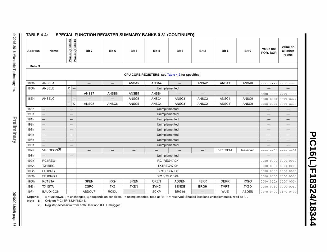
2
01
5-2
01
6 M
icroch
ip T
ech
no
log
y Inc.
Prelim
inary
DS
40
00
18
00
B-p
ag
e 3
3
PIC
16(L)F
18324/18344
18 ANSA0 --xx -xxx --uu -uuu
18 — —
― xxxx ---- uuuu ----
18 ANSC0 --xx xxxx --uu uuuu
ANSC0 xxxx xxxx uuuu uuuu
18 — —
19 — —
19 — —
19 — —
19 — —
19 — —
19 — —
19 — —
19 Reserved ---- --01 ---- --01
19 — —
19 0000 0000 0000 0000
19 0000 0000 0000 0000
19 0000 0000 0000 0000
19 0000 0000 0000 0000
19 RX9D 0000 000x 0000 000x
19 TX9D 0000 0010 0000 0010
19 ABDEN 01-0 0-00 01-0 0-00
TA
Ad Bit 0Value on:POR, BOR
Value on all other resets
Le , read as ‘0’.No
Bank 3
CPU CORE REGISTERS; see Table 4-2 for specifics
Ch ANSELA ― ― ANSA5 ANSA4 ― ANSA2 ANSA1
Dh ANSELB X ― Unimplemented
― ANSB7 ANSB6 ANSB5 ANSB4 ― ― ―
Eh ANSELC ― ― ― ANSC5 ANSC4 ANSC3 ANSC2 ANSC1
― X ANSC7 ANSC6 ANSC5 ANSC4 ANSC3 ANSC2 ANSC1
Fh ― ― Unimplemented
0h ― ― Unimplemented
1h ― ― Unimplemented
2h ― ― Unimplemented
3h ― ― Unimplemented
4h ― ― Unimplemented
5h ― ― Unimplemented
6h ― ― Unimplemented
7h VREGCON(1) ― ― ― ― ― ― VREGPM
8h ― ― Unimplemented
9h RC1REG RC1REG<7:0>
Ah TX1REG TX1REG<7:0>
Bh SP1BRGL SP1BRG<7:0>
Ch SP1BRGH SP1BRG<15:8>
Dh RC1STA SPEN RX9 SREN CREN ADDEN FERR OERR
Eh TX1STA CSRC TX9 TXEN SYNC SENDB BRGH TMRT
Fh BAUD1CON ABDOVF RCIDL — SCKP BRG16 — WUE
BLE 4-4: SPECIAL FUNCTION REGISTER SUMMARY BANKS 0-31 (CONTINUED)
dress Name
PIC
16(L
)F1
832
4
PIC
16(L
)F1
834
4
Bit 7 Bit 6 Bit 5 Bit 4 Bit 3 Bit 2 Bit 1
gend: x = unknown, u = unchanged, q =depends on condition, - = unimplemented, read as ‘0’, r = reserved. Shaded locations unimplementedte 1: Only on PIC16F18324/18344.
2: Register accessible from both User and ICD Debugger.
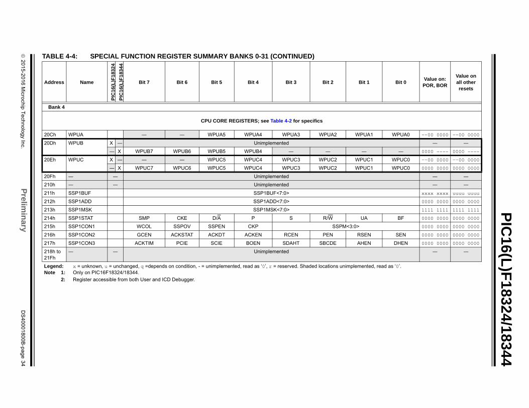
2
01
5-2
01
6 M
icroch
ip T
ech
no
log
y Inc.
Prelim
inary
DS
40
00
18
00
B-p
ag
e 3
4
PIC
16(L)F
18324/18344
20 WPUA0 --00 0000 --00 0000
20 ― ―
― 0000 ---- 0000 ----
20 WPUC0 --00 0000 --00 0000
WPUC0 0000 0000 0000 0000
20 ― ―
21 ― ―
21 xxxx xxxx uuuu uuuu
21 0000 0000 0000 0000
21 1111 1111 1111 1111
21 BF 0000 0000 0000 0000
21 0000 0000 0000 0000
21 SEN 0000 0000 0000 0000
21 DHEN 0000 0000 0000 0000
2121
― ―
TA
Ad Bit 0Value on:POR, BOR
Value on all other resets
Le , read as ‘0’.No
Bank 4
CPU CORE REGISTERS; see Table 4-2 for specifics
Ch WPUA ― ― WPUA5 WPUA4 WPUA3 WPUA2 WPUA1
Dh WPUB X ― Unimplemented
― X WPUB7 WPUB6 WPUB5 WPUB4 ― ― ―
Eh WPUC X ― ― ― WPUC5 WPUC4 WPUC3 WPUC2 WPUC1
― X WPUC7 WPUC6 WPUC5 WPUC4 WPUC3 WPUC2 WPUC1
Fh ― ― Unimplemented
0h ― ― Unimplemented
1h SSP1BUF SSP1BUF<7:0>
2h SSP1ADD SSP1ADD<7:0>
3h SSP1MSK SSP1MSK<7:0>
4h SSP1STAT SMP CKE D/A P S R/W UA
5h SSP1CON1 WCOL SSPOV SSPEN CKP SSPM<3:0>
6h SSP1CON2 GCEN ACKSTAT ACKDT ACKEN RCEN PEN RSEN
7h SSP1CON3 ACKTIM PCIE SCIE BOEN SDAHT SBCDE AHEN
8h to Fh
― ― Unimplemented
BLE 4-4: SPECIAL FUNCTION REGISTER SUMMARY BANKS 0-31 (CONTINUED)
dress Name
PIC
16(L
)F1
832
4
PIC
16(L
)F1
834
4
Bit 7 Bit 6 Bit 5 Bit 4 Bit 3 Bit 2 Bit 1
gend: x = unknown, u = unchanged, q =depends on condition, - = unimplemented, read as ‘0’, r = reserved. Shaded locations unimplementedte 1: Only on PIC16F18324/18344.
2: Register accessible from both User and ICD Debugger.
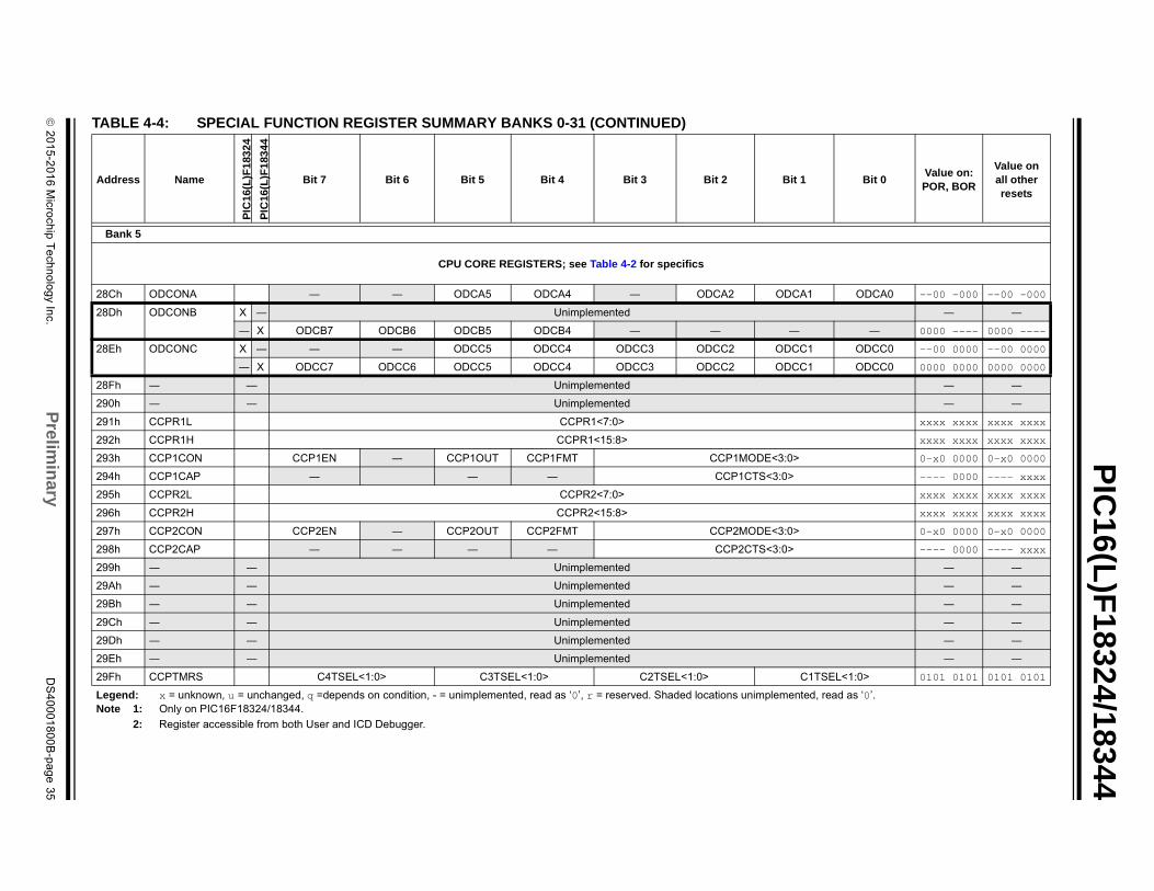
2
01
5-2
01
6 M
icroch
ip T
ech
no
log
y Inc.
Prelim
inary
DS
40
00
18
00
B-p
ag
e 3
5
PIC
16(L)F
18324/18344
28 ODCA0 --00 -000 --00 -000
28 ― ―
― 0000 ---- 0000 ----
28 ODCC0 --00 0000 --00 0000
ODCC0 0000 0000 0000 0000
28 ― ―
29 ― ―
29 xxxx xxxx xxxx xxxx
29 xxxx xxxx xxxx xxxx
29 0-x0 0000 0-x0 0000
29 ---- 0000 ---- xxxx
29 xxxx xxxx xxxx xxxx
29 xxxx xxxx xxxx xxxx
29 0-x0 0000 0-x0 0000
29 ---- 0000 ---- xxxx
29 ― ―
29 ― ―
29 ― ―
29 ― ―
29 ― ―
29 ― ―
29 TSEL<1:0> 0101 0101 0101 0101
TA
Ad Bit 0Value on:POR, BOR
Value on all other resets
Le , read as ‘0’.No
Bank 5
CPU CORE REGISTERS; see Table 4-2 for specifics
Ch ODCONA ― ― ODCA5 ODCA4 ― ODCA2 ODCA1
Dh ODCONB X ― Unimplemented
― X ODCB7 ODCB6 ODCB5 ODCB4 ― ― ―
Eh ODCONC X ― ― ― ODCC5 ODCC4 ODCC3 ODCC2 ODCC1
― X ODCC7 ODCC6 ODCC5 ODCC4 ODCC3 ODCC2 ODCC1
Fh ― — Unimplemented
0h ― ― Unimplemented
1h CCPR1L CCPR1<7:0>
2h CCPR1H CCPR1<15:8>
3h CCP1CON CCP1EN ― CCP1OUT CCP1FMT CCP1MODE<3:0>
4h CCP1CAP ― ― ― CCP1CTS<3:0>
5h CCPR2L CCPR2<7:0>
6h CCPR2H CCPR2<15:8>
7h CCP2CON CCP2EN ― CCP2OUT CCP2FMT CCP2MODE<3:0>
8h CCP2CAP ― ― ― ― CCP2CTS<3:0>
9h ― ― Unimplemented
Ah ― ― Unimplemented
Bh ― ― Unimplemented
Ch ― ― Unimplemented
Dh ― ― Unimplemented
Eh ― ― Unimplemented
Fh CCPTMRS C4TSEL<1:0> C3TSEL<1:0> C2TSEL<1:0> C1
BLE 4-4: SPECIAL FUNCTION REGISTER SUMMARY BANKS 0-31 (CONTINUED)
dress Name
PIC
16(L
)F1
832
4
PIC
16(L
)F1
834
4
Bit 7 Bit 6 Bit 5 Bit 4 Bit 3 Bit 2 Bit 1
gend: x = unknown, u = unchanged, q =depends on condition, - = unimplemented, read as ‘0’, r = reserved. Shaded locations unimplementedte 1: Only on PIC16F18324/18344.
2: Register accessible from both User and ICD Debugger.
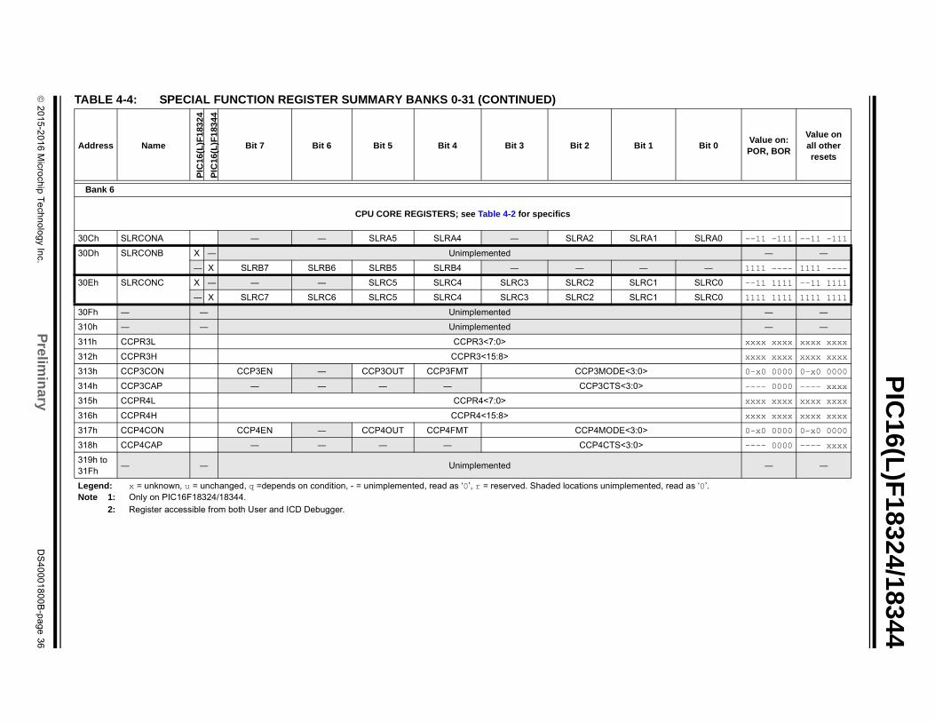
2
01
5-2
01
6 M
icroch
ip T
ech
no
log
y Inc.
Prelim
inary
DS
40
00
18
00
B-p
ag
e 3
6
PIC
16(L)F
18324/18344
30 SLRA0 --11 -111 --11 -111
30 ― ―
― 1111 ---- 1111 ----
30 SLRC0 --11 1111 --11 1111
SLRC0 1111 1111 1111 1111
30 ― ―
31 ― ―
31 xxxx xxxx xxxx xxxx
31 xxxx xxxx xxxx xxxx
31 0-x0 0000 0-x0 0000
31 ---- 0000 ---- xxxx
31 xxxx xxxx xxxx xxxx
31 xxxx xxxx xxxx xxxx
31 0-x0 0000 0-x0 0000
31 ---- 0000 ---- xxxx
3131
― ―
TA
Ad Bit 0Value on:POR, BOR
Value on all other resets
Le , read as ‘0’.No
Bank 6
CPU CORE REGISTERS; see Table 4-2 for specifics
Ch SLRCONA ― ― SLRA5 SLRA4 ― SLRA2 SLRA1
Dh SLRCONB X ― Unimplemented
― X SLRB7 SLRB6 SLRB5 SLRB4 ― ― ―
Eh SLRCONC X ― ― ― SLRC5 SLRC4 SLRC3 SLRC2 SLRC1
― X SLRC7 SLRC6 SLRC5 SLRC4 SLRC3 SLRC2 SLRC1
Fh ― ― Unimplemented
0h ― ― Unimplemented
1h CCPR3L CCPR3<7:0>
2h CCPR3H CCPR3<15:8>
3h CCP3CON CCP3EN ― CCP3OUT CCP3FMT CCP3MODE<3:0>
4h CCP3CAP ― ― ― ― CCP3CTS<3:0>
5h CCPR4L CCPR4<7:0>
6h CCPR4H CCPR4<15:8>
7h CCP4CON CCP4EN ― CCP4OUT CCP4FMT CCP4MODE<3:0>
8h CCP4CAP ― ― ― ― CCP4CTS<3:0>
9h to Fh
― ― Unimplemented
BLE 4-4: SPECIAL FUNCTION REGISTER SUMMARY BANKS 0-31 (CONTINUED)
dress Name
PIC
16(L
)F1
832
4
PIC
16(L
)F1
834
4
Bit 7 Bit 6 Bit 5 Bit 4 Bit 3 Bit 2 Bit 1
gend: x = unknown, u = unchanged, q =depends on condition, - = unimplemented, read as ‘0’, r = reserved. Shaded locations unimplementedte 1: Only on PIC16F18324/18344.
2: Register accessible from both User and ICD Debugger.
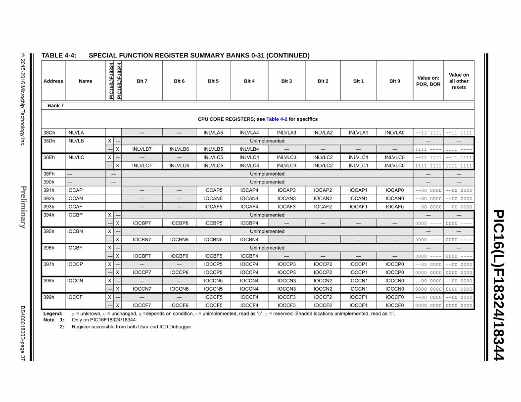
2
01
5-2
01
6 M
icroch
ip T
ech
no
log
y Inc.
Prelim
inary
DS
40
00
18
00
B-p
ag
e 3
7
PIC
16(L)F
18324/18344
38 INLVLA0 --11 1111 --11 1111
38 ― ―
― 1111 ---- 1111 ----
38 INLVLC0 --11 1111 --11 1111
INLVLC0 1111 1111 1111 1111
38 ― ―
39 ― ―
39 IOCAP0 --00 0000 --00 0000
39 IOCAN0 --00 0000 --00 0000
39 IOCAF0 --00 0000 --00 0000
39 ― ―
― 0000 ---- 0000 ----
39 ― ―
― 0000 ---- 0000 ----
39 ― ―
― 0000 ---- 0000 ----
39 IOCCP0 --00 0000 --00 0000
IOCCP0 0000 0000 0000 0000
39 IOCCN0 --00 0000 --00 0000
IOCCN0 0000 0000 0000 0000
39 IOCCF0 --00 0000 --00 0000
IOCCF0 0000 0000 0000 0000
TA
Ad Bit 0Value on:POR, BOR
Value on all other resets
Le , read as ‘0’.No
Bank 7
CPU CORE REGISTERS; see Table 4-2 for specifics
Ch INLVLA ― ― INLVLA5 INLVLA4 INLVLA3 INLVLA2 INLVLA1
Dh INLVLB X ― Unimplemented
― X INLVLB7 INLVLB6 INLVLB5 INLVLB4 ― ― ―
Eh INLVLC X ― ― ― INLVLC5 INLVLC4 INLVLC3 INLVLC2 INLVLC1
― X INLVLC7 INLVLC6 INLVLC5 INLVLC4 INLVLC3 INLVLC2 INLVLC1
Fh ― ― Unimplemented
0h ― ― Unimplemented
1h IOCAP ― ― IOCAP5 IOCAP4 IOCAP3 IOCAP2 IOCAP1
2h IOCAN ― ― IOCAN5 IOCAN4 IOCAN3 IOCAN2 IOCAN1
3h IOCAF ― ― IOCAF5 IOCAF4 IOCAF3 IOCAF2 IOCAF1
4h IOCBP X ― Unimplemented
― X IOCBP7 IOCBP6 IOCBP5 IOCBP4 ― ― ―
5h IOCBN X ― Unimplemented
― X IOCBN7 IOCBN6 IOCBN5 IOCBN4 ― ― ―
6h IOCBF X ― Unimplemented
― X IOCBF7 IOCBF6 IOCBF5 IOCBF4 ― ― ―
7h IOCCP X ― ― ― IOCCP5 IOCCP4 IOCCP3 IOCCP2 IOCCP1
― X IOCCP7 IOCCP6 IOCCP5 IOCCP4 IOCCP3 IOCCP2 IOCCP1
8h IOCCN X ― ― ― IOCCN5 IOCCN4 IOCCN3 IOCCN2 IOCCN1
― X IOCCN7 IOCCN6 IOCCN5 IOCCN4 IOCCN3 IOCCN2 IOCCN1
9h IOCCF X ― ― ― IOCCF5 IOCCF4 IOCCF3 IOCCF2 IOCCF1
― X IOCCF7 IOCCF6 IOCCF5 IOCCF4 IOCCF3 IOCCF2 IOCCF1
BLE 4-4: SPECIAL FUNCTION REGISTER SUMMARY BANKS 0-31 (CONTINUED)
dress Name
PIC
16(L
)F1
832
4
PIC
16(L
)F1
834
4
Bit 7 Bit 6 Bit 5 Bit 4 Bit 3 Bit 2 Bit 1
gend: x = unknown, u = unchanged, q =depends on condition, - = unimplemented, read as ‘0’, r = reserved. Shaded locations unimplementedte 1: Only on PIC16F18324/18344.
2: Register accessible from both User and ICD Debugger.
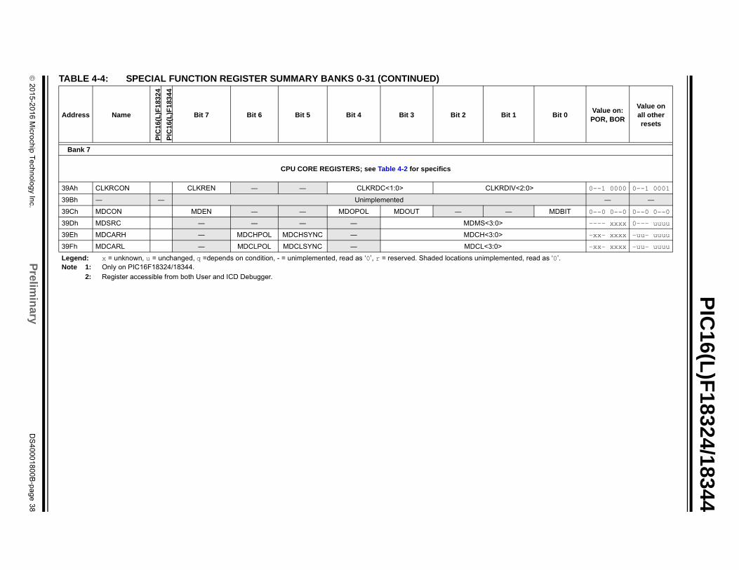
2
01
5-2
01
6 M
icroch
ip T
ech
no
log
y Inc.
Prelim
inary
DS
40
00
18
00
B-p
ag
e 3
8
PIC
16(L)F
18324/18344
39 :0> 0--1 0000 0--1 0001
39 ― ―
39 MDBIT 0--0 0--0 0--0 0--0
39 ---- xxxx 0--- uuuu
39 -xx- xxxx -uu- uuuu
39 -xx- xxxx -uu- uuuu
TA
Ad Bit 0Value on:POR, BOR
Value on all other resets
Le , read as ‘0’.No
Bank 7
CPU CORE REGISTERS; see Table 4-2 for specifics
Ah CLKRCON CLKREN ― ― CLKRDC<1:0> CLKRDIV<2
Bh ― ― Unimplemented
Ch MDCON MDEN ― ― MDOPOL MDOUT ― ―
Dh MDSRC ― ― ― ― MDMS<3:0>
Eh MDCARH ― MDCHPOL MDCHSYNC ― MDCH<3:0>
Fh MDCARL ― MDCLPOL MDCLSYNC ― MDCL<3:0>
BLE 4-4: SPECIAL FUNCTION REGISTER SUMMARY BANKS 0-31 (CONTINUED)
dress Name
PIC
16(L
)F1
832
4
PIC
16(L
)F1
834
4
Bit 7 Bit 6 Bit 5 Bit 4 Bit 3 Bit 2 Bit 1
gend: x = unknown, u = unchanged, q =depends on condition, - = unimplemented, read as ‘0’, r = reserved. Shaded locations unimplementedte 1: Only on PIC16F18324/18344.
2: Register accessible from both User and ICD Debugger.
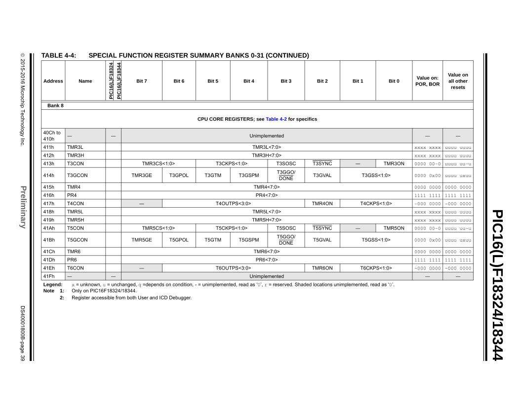
2
01
5-2
01
6 M
icroch
ip T
ech
no
log
y Inc.
Prelim
inary
DS
40
00
18
00
B-p
ag
e 3
9
PIC
16(L)F
18324/18344
4041
― ―
41 xxxx xxxx uuuu uuuu
41 xxxx xxxx uuuu uuuu
41 TMR3ON 0000 00-0 uuuu uu-u
41 GSS<1:0> 0000 0x00 uuuu uxuu
41 0000 0000 0000 0000
41 1111 1111 1111 1111
41 KPS<1:0> -000 0000 -000 0000
41 xxxx xxxx uuuu uuuu
41 xxxx xxxx uuuu uuuu
41 TMR5ON 0000 00-0 uuuu uu-u
41 GSS<1:0> 0000 0x00 uuuu uxuu
41 0000 0000 0000 0000
41 1111 1111 1111 1111
41 KPS<1:0> -000 0000 -000 0000
41 ― ―
TA
Ad Bit 0Value on:POR, BOR
Value on all other resets
Le , read as ‘0’.No
Bank 8
CPU CORE REGISTERS; see Table 4-2 for specifics
Ch to 0h
― ― Unimplemented
1h TMR3L TMR3L<7:0>
2h TMR3H TMR3H<7:0>
3h T3CON TMR3CS<1:0> T3CKPS<1:0> T3SOSC T3SYNC ―
4h T3GCON TMR3GE T3GPOL T3GTM T3GSPMT3GGO/ DONE
T3GVAL T3
5h TMR4 TMR4<7:0>
6h PR4 PR4<7:0>
7h T4CON ― T4OUTPS<3:0> TMR4ON T4C
8h TMR5L TMR5L<7:0>
9h TMR5H TMR5H<7:0>
Ah T5CON TMR5CS<1:0> T5CKPS<1:0> T5SOSC T5SYNC ―
Bh T5GCON TMR5GE T5GPOL T5GTM T5GSPMT5GGO/ DONE
T5GVAL T5
Ch TMR6 TMR6<7:0>
Dh PR6 PR6<7:0>
Eh T6CON ― T6OUTPS<3:0> TMR6ON T6C
Fh ― ― Unimplemented
BLE 4-4: SPECIAL FUNCTION REGISTER SUMMARY BANKS 0-31 (CONTINUED)
dress Name
PIC
16(L
)F1
832
4
PIC
16(L
)F1
834
4
Bit 7 Bit 6 Bit 5 Bit 4 Bit 3 Bit 2 Bit 1
gend: x = unknown, u = unchanged, q =depends on condition, - = unimplemented, read as ‘0’, r = reserved. Shaded locations unimplementedte 1: Only on PIC16F18324/18344.
2: Register accessible from both User and ICD Debugger.
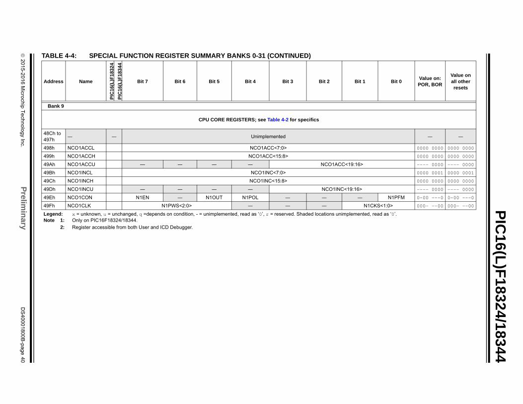
2
01
5-2
01
6 M
icroch
ip T
ech
no
log
y Inc.
Prelim
inary
DS
40
00
18
00
B-p
ag
e 4
0
PIC
16(L)F
18324/18344
4849
― ―
49 0000 0000 0000 0000
49 0000 0000 0000 0000
49 ---- 0000 ---- 0000
49 0000 0001 0000 0001
49 0000 0000 0000 0000
49 ---- 0000 ---- 0000
49 N1PFM 0-00 ---0 0-00 ---0
49 CKS<1:0> 000- --00 000- --00
TA
Ad Bit 0Value on:POR, BOR
Value on all other resets
Le , read as ‘0’.No
Bank 9
CPU CORE REGISTERS; see Table 4-2 for specifics
Ch to 7h
― ― Unimplemented
8h NCO1ACCL NCO1ACC<7:0>
9h NCO1ACCH NCO1ACC<15:8>
Ah NCO1ACCU — ― ― ― NCO1ACC<19:16>
Bh NCO1INCL NCO1INC<7:0>
Ch NCO1INCH NCO1INC<15:8>
Dh NCO1INCU ― ― ― ― NCO1INC<19:16>
Eh NCO1CON N1EN ― N1OUT N1POL ― ― ―
Fh NCO1CLK N1PWS<2:0> ― ― ― N1
BLE 4-4: SPECIAL FUNCTION REGISTER SUMMARY BANKS 0-31 (CONTINUED)
dress Name
PIC
16(L
)F1
832
4
PIC
16(L
)F1
834
4
Bit 7 Bit 6 Bit 5 Bit 4 Bit 3 Bit 2 Bit 1
gend: x = unknown, u = unchanged, q =depends on condition, - = unimplemented, read as ‘0’, r = reserved. Shaded locations unimplementedte 1: Only on PIC16F18324/18344.
2: Register accessible from both User and ICD Debugger.
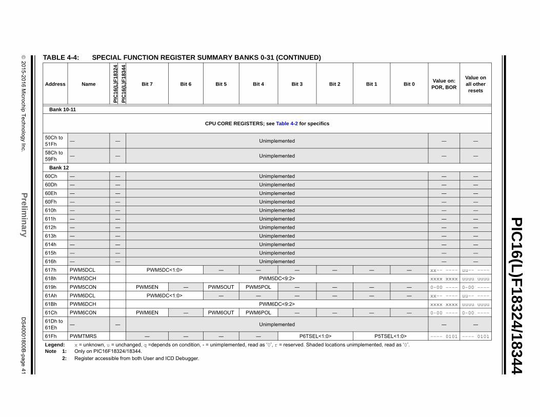
2
01
5-2
01
6 M
icroch
ip T
ech
no
log
y Inc.
Prelim
inary
DS
40
00
18
00
B-p
ag
e 4
1
PIC
16(L)F
18324/18344
5051
― ―
5859
― ―
60 ― ―
60 ― ―
60 ― ―
60 ― ―
61 ― ―
61 ― ―
61 ― ―
61 ― ―
61 ― ―
61 ― ―
61 ― ―
61 ― xx-- ---- uu-- ----
61 xxxx xxxx uuuu uuuu
61 ― 0-00 ---- 0-00 ----
61 ― xx-- ---- uu-- ----
61 xxxx xxxx uuuu uuuu
61 ― 0-00 ---- 0-00 ----
6161
― ―
61 TSEL<1:0> ---- 0101 ---- 0101
TA
Ad Bit 0Value on:POR, BOR
Value on all other resets
Le , read as ‘0’.No
Bank 10-11
CPU CORE REGISTERS; see Table 4-2 for specifics
Ch to Fh
― ― Unimplemented
Ch to Fh
― ― Unimplemented
Bank 12
Ch ― ― Unimplemented
Dh ― ― Unimplemented
Eh ― ― Unimplemented
Fh ― ― Unimplemented
0h ― ― Unimplemented
1h ― ― Unimplemented
2h ― ― Unimplemented
3h ― ― Unimplemented
4h ― ― Unimplemented
5h ― ― Unimplemented
6h ― ― Unimplemented
7h PWM5DCL PWM5DC<1:0> ― ― ― ― ―
8h PWM5DCH PWM5DC<9:2>
9h PWM5CON PWM5EN ― PWM5OUT PWM5POL ― ― ―
Ah PWM6DCL PWM6DC<1:0> ― ― ― ― ―
Bh PWM6DCH PWM6DC<9:2>
Ch PWM6CON PWM6EN ― PWM6OUT PWM6POL ― ― ―
Dh to Eh
― ― Unimplemented
Fh PWMTMRS ― ― ― ― P6TSEL<1:0> P5
BLE 4-4: SPECIAL FUNCTION REGISTER SUMMARY BANKS 0-31 (CONTINUED)
dress Name
PIC
16(L
)F1
832
4
PIC
16(L
)F1
834
4
Bit 7 Bit 6 Bit 5 Bit 4 Bit 3 Bit 2 Bit 1
gend: x = unknown, u = unchanged, q =depends on condition, - = unimplemented, read as ‘0’, r = reserved. Shaded locations unimplementedte 1: Only on PIC16F18324/18344.
2: Register accessible from both User and ICD Debugger.

2
01
5-2
01
6 M
icroch
ip T
ech
no
log
y Inc.
Prelim
inary
DS
40
00
18
00
B-p
ag
e 4
2
PIC
16(L)F
18324/18344
68 ― ―
68 ― ―
68 ― ―
68 ― ―
69 ― ―
69 CS ---- ---0 ---- ---0
69 ---- 0000 ---- 0000
69 --00 0000 --00 0000
69 --00 0000 --00 0000
69 0> 00-- -000 00-- -000
69 POLA --x- 0000 --x- 0000
69 ― 0001 01-- 0001 01--
69 AS0E ---0 0000 ---0 0000
69 STRA 0000 0000 0000 0000
6969
― ―
TA
Ad Bit 0Value on:POR, BOR
Value on all other resets
Le , read as ‘0’.No
Bank 13
CPU CORE REGISTERS; see Table 4-2 for specifics
Ch ― ― Unimplemented
Dh ― ― Unimplemented
Eh ― ― Unimplemented
Fh ― ― Unimplemented
0h ― ― Unimplemented
1h CWG1CLKCON ― ― ― ― ― ― ―
2h CWG1DAT ― ― ― ― DAT<3:0>
3h CWG1DBR ― ― DBR<5:0>
4h CWG1DBF ― ― DBF<5:0>
5h CWG1CON0 EN LD ― ― ― MODE<2:
6h CWG1CON1 ― ― IN ― POLD POLC POLB
7h CWG1AS0 SHUTDOWN REN LSBD<1:0> LSAC<1:0> ―
8h CWG1AS1 ― ― ― AS4E AS3E AS2E AS1E
9h CWG1STR OVRD OVRC OVRB OVRA STRD STRC STRB
Ah to Fh
― ― Unimplemented
BLE 4-4: SPECIAL FUNCTION REGISTER SUMMARY BANKS 0-31 (CONTINUED)
dress Name
PIC
16(L
)F1
832
4
PIC
16(L
)F1
834
4
Bit 7 Bit 6 Bit 5 Bit 4 Bit 3 Bit 2 Bit 1
gend: x = unknown, u = unchanged, q =depends on condition, - = unimplemented, read as ‘0’, r = reserved. Shaded locations unimplementedte 1: Only on PIC16F18324/18344.
2: Register accessible from both User and ICD Debugger.
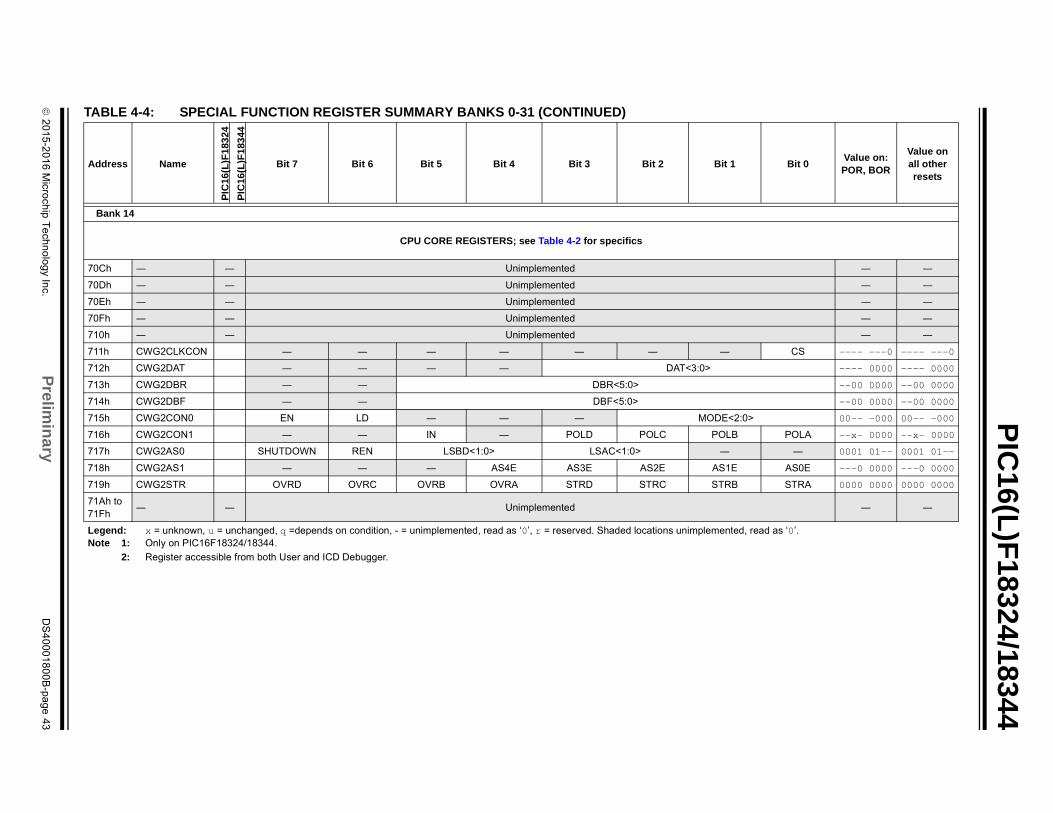
2
01
5-2
01
6 M
icroch
ip T
ech
no
log
y Inc.
Prelim
inary
DS
40
00
18
00
B-p
ag
e 4
3
PIC
16(L)F
18324/18344
70 ― ―
70 ― ―
70 ― ―
70 ― ―
71 ― ―
71 CS ---- ---0 ---- ---0
71 ---- 0000 ---- 0000
71 --00 0000 --00 0000
71 --00 0000 --00 0000
71 0> 00-- -000 00-- -000
71 POLA --x- 0000 --x- 0000
71 ― 0001 01-- 0001 01--
71 AS0E ---0 0000 ---0 0000
71 STRA 0000 0000 0000 0000
7171
― ―
TA
Ad Bit 0Value on:POR, BOR
Value on all other resets
Le , read as ‘0’.No
Bank 14
CPU CORE REGISTERS; see Table 4-2 for specifics
Ch ― ― Unimplemented
Dh ― ― Unimplemented
Eh ― ― Unimplemented
Fh ― ― Unimplemented
0h ― ― Unimplemented
1h CWG2CLKCON ― ― ― ― ― ― ―
2h CWG2DAT ― ― ― ― DAT<3:0>
3h CWG2DBR ― ― DBR<5:0>
4h CWG2DBF ― ― DBF<5:0>
5h CWG2CON0 EN LD ― ― ― MODE<2:
6h CWG2CON1 ― ― IN ― POLD POLC POLB
7h CWG2AS0 SHUTDOWN REN LSBD<1:0> LSAC<1:0> ―
8h CWG2AS1 ― ― ― AS4E AS3E AS2E AS1E
9h CWG2STR OVRD OVRC OVRB OVRA STRD STRC STRB
Ah toFh
― ― Unimplemented
BLE 4-4: SPECIAL FUNCTION REGISTER SUMMARY BANKS 0-31 (CONTINUED)
dress Name
PIC
16(L
)F1
832
4
PIC
16(L
)F1
834
4
Bit 7 Bit 6 Bit 5 Bit 4 Bit 3 Bit 2 Bit 1
gend: x = unknown, u = unchanged, q =depends on condition, - = unimplemented, read as ‘0’, r = reserved. Shaded locations unimplementedte 1: Only on PIC16F18324/18344.
2: Register accessible from both User and ICD Debugger.
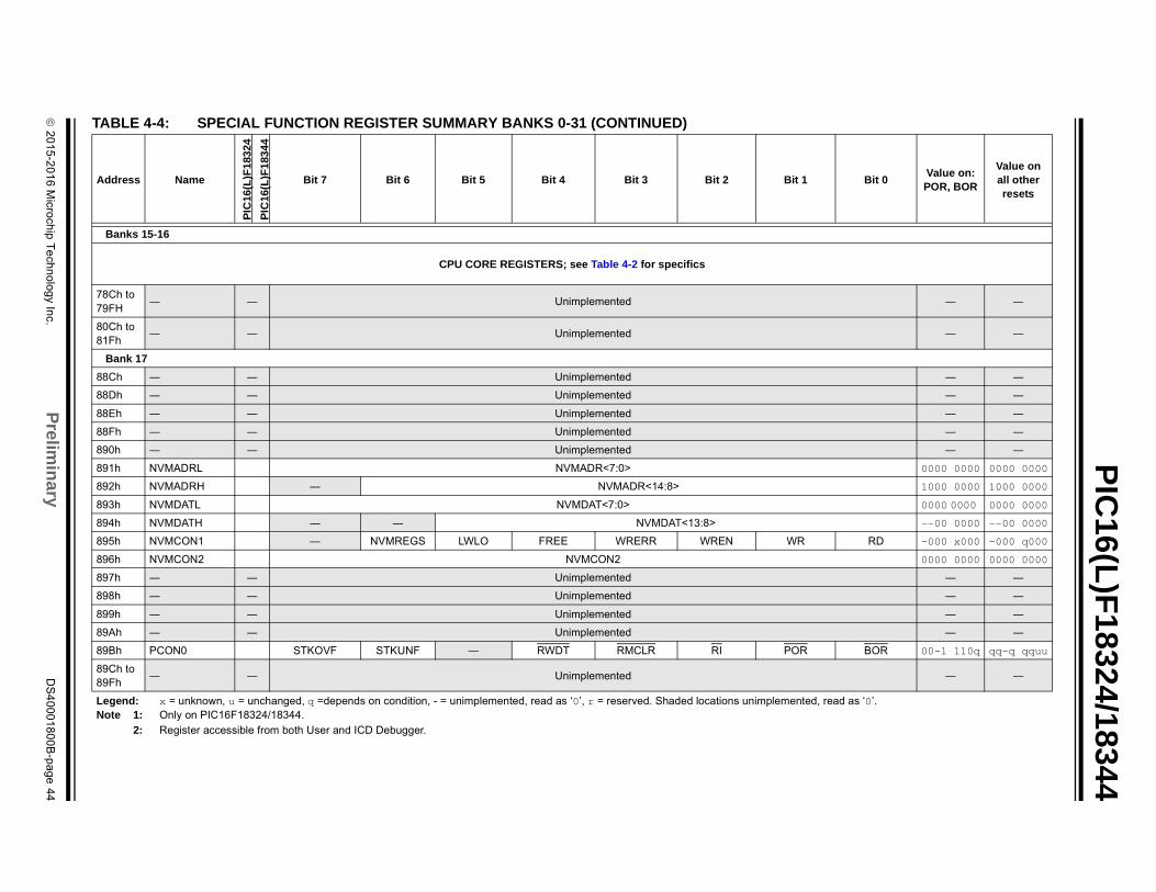
2
01
5-2
01
6 M
icroch
ip T
ech
no
log
y Inc.
Prelim
inary
DS
40
00
18
00
B-p
ag
e 4
4
PIC
16(L)F
18324/18344
7879
― ―
8081
― ―
88 ― ―
88 ― ―
88 ― ―
88 ― ―
89 ― ―
89 0000 0000 0000 0000
89 1000 0000 1000 0000
89 0000 0000 0000 0000
89 --00 0000 --00 0000
89 RD -000 x000 -000 q000
89 0000 0000 0000 0000
89 ― ―
89 ― ―
89 ― ―
89 ― ―
89 BOR 00-1 110q qq-q qquu
8989
― ―
TA
Ad Bit 0Value on:POR, BOR
Value on all other resets
Le , read as ‘0’.No
Banks 15-16
CPU CORE REGISTERS; see Table 4-2 for specifics
Ch toFH
― ― Unimplemented
Ch toFh
― ― Unimplemented
Bank 17
Ch ― ― Unimplemented
Dh ― ― Unimplemented
Eh ― ― Unimplemented
Fh ― ― Unimplemented
0h ― ― Unimplemented
1h NVMADRL NVMADR<7:0>
2h NVMADRH ― NVMADR<14:8>
3h NVMDATL NVMDAT<7:0>
4h NVMDATH ― ― NVMDAT<13:8>
5h NVMCON1 ― NVMREGS LWLO FREE WRERR WREN WR
6h NVMCON2 NVMCON2
7h ― ― Unimplemented
8h ― ― Unimplemented
9h ― ― Unimplemented
Ah ― ― Unimplemented
Bh PCON0 STKOVF STKUNF ― RWDT RMCLR RI POR
Ch to Fh
― ― Unimplemented
BLE 4-4: SPECIAL FUNCTION REGISTER SUMMARY BANKS 0-31 (CONTINUED)
dress Name
PIC
16(L
)F1
832
4
PIC
16(L
)F1
834
4
Bit 7 Bit 6 Bit 5 Bit 4 Bit 3 Bit 2 Bit 1
gend: x = unknown, u = unchanged, q =depends on condition, - = unimplemented, read as ‘0’, r = reserved. Shaded locations unimplementedte 1: Only on PIC16F18324/18344.
2: Register accessible from both User and ICD Debugger.
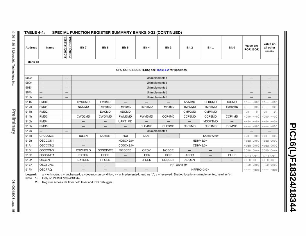
2
01
5-2
01
6 M
icroch
ip T
ech
no
log
y Inc.
Prelim
inary
DS
40
00
18
00
B-p
ag
e 4
5
PIC
16(L)F
18324/18344
90 ― ―
90 ― ―
90 ― ―
90 ― ―
91 ― ―
91 IOCMD 00-- -000 00-- -000
91 TMR0MD 0--- -000 0--- -000
91 ― -00- --0- -00- --0-
91 CCP1MD -000 --00 -000 --00
91 D ― --0- --0- --0- --0-
91 DSMMD ---- -000 ---- -000
91 ― ―
91 > 000- -000 000- -000
91 -qqq 0000 -qqq 0000
91 -qqq 0000 -qqq 0000
91 ― 0000 0--- 0000 0---
91 PLLR qq-q qq-q qq-q qq-q
91 ― 00-0 00-- 00-0 00--
91 --10 0000 --10 0000
91 ---- -qqq ---- -qqq
TA
Ad Bit 0Value on:POR, BOR
Value on all other resets
Le , read as ‘0’.No
Bank 18
CPU CORE REGISTERS; see Table 4-2 for specifics
Ch ― ― Unimplemented
Dh ― ― Unimplemented
Eh ― ― Unimplemented
Fh ― ― Unimplemented
0h ― ― Unimplemented
1h PMD0 SYSCMD FVRMD ― ― ― NVMMD CLKRMD
2h PMD1 NCOMD TMR6MD TMR5MD TMR4MD TMR3MD TMR2MD TMR1MD
3h PMD2 ― DACMD ADCMD ― ― CMP2MD CMP1MD
4h PMD3 CWG2MD CWG1MD PWM6MD PWM5MD CCP4MD CCP3MD CCP2MD
5h PMD4 ― ― UART1MD ― ― ― MSSP1M
6h PMD5 ― ― ― CLC4MD CLC3MD CLC2MD CLC1MD
7h ― ― Unimplemented
8h CPUDOZE IDLEN DOZEN ROI DOE ― DOZE<2:0
9h OSCCON1 ― NOSC<2:0> NDIV<3:0>
Ah OSCCON2 ― COSC<2:0> CDIV<3:0>
Bh OSCCON3 CSWHOLD SOSCPWR SOSCBE ORDY NOSCR ― ―
Ch OSCSTAT1 EXTOR HFOR ― LFOR SOR ADOR ―
Dh OSCEN EXTOEN HFOEN ― LFOEN SOSCEN ADOEN ―
Eh OSCTUNE ― ― HFTUN<5:0>
Fh OSCFRQ ― ― ― ― HFFRQ<3:0>
BLE 4-4: SPECIAL FUNCTION REGISTER SUMMARY BANKS 0-31 (CONTINUED)
dress Name
PIC
16(L
)F1
832
4
PIC
16(L
)F1
834
4
Bit 7 Bit 6 Bit 5 Bit 4 Bit 3 Bit 2 Bit 1
gend: x = unknown, u = unchanged, q =depends on condition, - = unimplemented, read as ‘0’, r = reserved. Shaded locations unimplementedte 1: Only on PIC16F18324/18344.
2: Register accessible from both User and ICD Debugger.
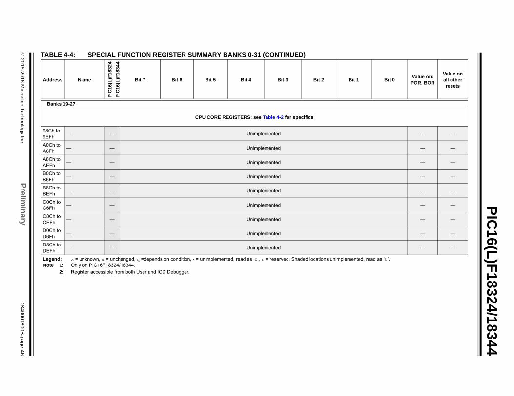
2
01
5-2
01
6 M
icroch
ip T
ech
no
log
y Inc.
Prelim
inary
DS
40
00
18
00
B-p
ag
e 4
6
PIC
16(L)F
18324/18344
989E
— —
A0A6
— —
A8AE
— —
B0B6
— —
B8BE
— —
C0C6
— —
C8CE
— —
D0D6
— —
D8DE
— —
TA
Ad Bit 0Value on:POR, BOR
Value on all other resets
Le , read as ‘0’.No
Banks 19-27
CPU CORE REGISTERS; see Table 4-2 for specifics
Ch toFh
— — Unimplemented
Ch to Fh
— — Unimplemented
Ch to Fh
— — Unimplemented
Ch to Fh
— — Unimplemented
Ch to Fh
— — Unimplemented
Ch to Fh
— — Unimplemented
Ch to Fh
— — Unimplemented
Ch to Fh
— — Unimplemented
Ch to Fh
— — Unimplemented
BLE 4-4: SPECIAL FUNCTION REGISTER SUMMARY BANKS 0-31 (CONTINUED)
dress Name
PIC
16(L
)F1
832
4
PIC
16(L
)F1
834
4
Bit 7 Bit 6 Bit 5 Bit 4 Bit 3 Bit 2 Bit 1
gend: x = unknown, u = unchanged, q =depends on condition, - = unimplemented, read as ‘0’, r = reserved. Shaded locations unimplementedte 1: Only on PIC16F18324/18344.
2: Register accessible from both User and ICD Debugger.
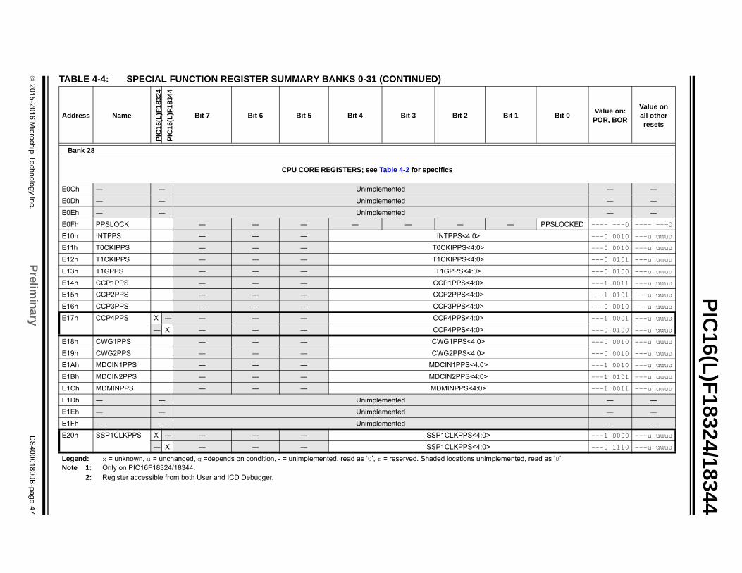
2
01
5-2
01
6 M
icroch
ip T
ech
no
log
y Inc.
Prelim
inary
DS
40
00
18
00
B-p
ag
e 4
7
PIC
16(L)F
18324/18344
E0 ― ―
E0 ― ―
E0 ― ―
E0 PPSLOCKED ---- ---0 ---- ---0
E1 ---0 0010 ---u uuuu
E1 ---0 0010 ---u uuuu
E1 ---0 0101 ---u uuuu
E1 ---0 0100 ---u uuuu
E1 ---1 0011 ---u uuuu
E1 ---1 0101 ---u uuuu
E1 ---0 0010 ---u uuuu
E1 ---1 0001 ---u uuuu
---0 0100 ---u uuuu
E1 ---0 0010 ---u uuuu
E1 ---0 0010 ---u uuuu
E1 ---1 0010 ---u uuuu
E1 ---1 0101 ---u uuuu
E1 ---1 0011 ---u uuuu
E1 ― ―
E1 ― ―
E1 ― ―
E2 ---1 0000 ---u uuuu
---0 1110 ---u uuuu
TA
Ad Bit 0Value on:POR, BOR
Value on all other resets
Le , read as ‘0’.No
Bank 28
CPU CORE REGISTERS; see Table 4-2 for specifics
Ch ― ― Unimplemented
Dh ― ― Unimplemented
Eh ― ― Unimplemented
Fh PPSLOCK ― ― ― ― ― ― ―
0h INTPPS ― ― ― INTPPS<4:0>
1h T0CKIPPS ― ― ― T0CKIPPS<4:0>
2h T1CKIPPS ― ― ― T1CKIPPS<4:0>
3h T1GPPS ― ― ― T1GPPS<4:0>
4h CCP1PPS ― ― ― CCP1PPS<4:0>
5h CCP2PPS ― ― ― CCP2PPS<4:0>
6h CCP3PPS ― ― ― CCP3PPS<4:0>
7h CCP4PPS X ― ― ― ― CCP4PPS<4:0>
― X ― ― ― CCP4PPS<4:0>
8h CWG1PPS ― ― ― CWG1PPS<4:0>
9h CWG2PPS ― ― ― CWG2PPS<4:0>
Ah MDCIN1PPS ― ― ― MDCIN1PPS<4:0>
Bh MDCIN2PPS ― ― ― MDCIN2PPS<4:0>
Ch MDMINPPS ― ― ― MDMINPPS<4:0>
Dh ― ― Unimplemented
Eh ― ― Unimplemented
Fh ― ― Unimplemented
0h SSP1CLKPPS X ― ― ― ― SSP1CLKPPS<4:0>
― X ― ― ― SSP1CLKPPS<4:0>
BLE 4-4: SPECIAL FUNCTION REGISTER SUMMARY BANKS 0-31 (CONTINUED)
dress Name
PIC
16(L
)F1
832
4
PIC
16(L
)F1
834
4
Bit 7 Bit 6 Bit 5 Bit 4 Bit 3 Bit 2 Bit 1
gend: x = unknown, u = unchanged, q =depends on condition, - = unimplemented, read as ‘0’, r = reserved. Shaded locations unimplementedte 1: Only on PIC16F18324/18344.
2: Register accessible from both User and ICD Debugger.
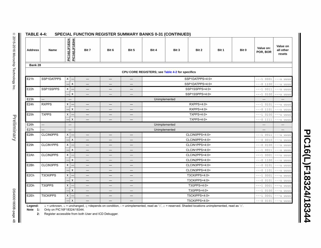
2
01
5-2
01
6 M
icroch
ip T
ech
no
log
y Inc.
Prelim
inary
DS
40
00
18
00
B-p
ag
e 4
8
PIC
16(L)F
18324/18344
E2 ---1 0001 ---u uuuu
---0 1100 ---u uuuu
E2 ---1 0011 ---u uuuu
---1 0100 ---u uuuu
E2 ― ―
E2 ---1 0101 ---u uuuu
---0 1101 ---u uuuu
E2 ---1 0100 ---u uuuu
---0 1111 ---u uuuu
E2 ― ―
E2 ― ―
E2 ---1 0011 ---u uuuu
---0 0010 ---u uuuu
E2 ---0 0100 ---u uuuu
---1 0011 ---u uuuu
E2 ---1 0001 ---u uuuu
---0 1100 ---u uuuu
E2 ---0 0101 ---u uuuu
---0 1101 ---u uuuu
E2 ---1 0001 ---u uuuu
---0 0101 ---u uuuu
E2 ---1 0001 ---u uuuu
---1 0100 ---u uuuu
E2 ---1 0001 ---u uuuu
---0 0101 ---u uuuu
TA
Ad Bit 0Value on:POR, BOR
Value on all other resets
Le , read as ‘0’.No
Bank 28
CPU CORE REGISTERS; see Table 4-2 for specifics
1h SSP1DATPPS X ― ― ― ― SSP1DATPPS<4:0>
― X ― ― ― SSP1DATPPS<4:0>
2h SSP1SSPPS X ― ― ― ― SSP1SSPPS<4:0>
― X ― ― ― SSP1SSPPS<4:0>
3h ― ― Unimplemented
4h RXPPS X ― ― ― ― RXPPS<4:0>
― X ― ― ― RXPPS<4:0>
5h TXPPS X ― ― ― ― TXPPS<4:0>
― X ― ― ― TXPPS<4:0>
6h ― ― Unimplemented
7h ― ― Unimplemented
8h CLCIN0PPS X ― ― ― ― CLCIN0PPS<4:0>
― X ― ― ― CLCIN0PPS<4:0>
9h CLCIN1PPS X ― ― ― ― CLCIN1PPS<4:0>
― X ― ― ― CLCIN1PPS<4:0>
Ah CLCIN2PPS X ― ― ― ― CLCIN2PPS<4:0>
― X ― ― ― CLCIN2PPS<4:0>
Bh CLCIN3PPS X ― ― ― ― CLCIN3PPS<4:0>
― X ― ― ― CLCIN3PPS<4:0>
Ch T3CKIPPS X ― ― ― ― T3CKIPPS<4:0>
― X ― ― ― T3CKIPPS<4:0>
Dh T3GPPS X ― ― ― ― T3GPPS<4:0>
― X ― ― ― T3GPPS<4:0>
Eh T5CKIPPS X ― ― ― ― T5CKIPPS<4:0>
― X ― ― ― T5CKIPPS<4:0>
BLE 4-4: SPECIAL FUNCTION REGISTER SUMMARY BANKS 0-31 (CONTINUED)
dress Name
PIC
16(L
)F1
832
4
PIC
16(L
)F1
834
4
Bit 7 Bit 6 Bit 5 Bit 4 Bit 3 Bit 2 Bit 1
gend: x = unknown, u = unchanged, q =depends on condition, - = unimplemented, read as ‘0’, r = reserved. Shaded locations unimplementedte 1: Only on PIC16F18324/18344.
2: Register accessible from both User and ICD Debugger.
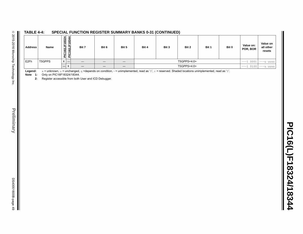
2
01
5-2
01
6 M
icroch
ip T
ech
no
log
y Inc.
Prelim
inary
DS
40
00
18
00
B-p
ag
e 4
9
PIC
16(L)F
18324/18344
E2 ---1 0001 ---u uuuu
---1 0100 ---u uuuu
TA
Ad Bit 0Value on:POR, BOR
Value on all other resets
Le , read as ‘0’.No
Fh T5GPPS X ― ― ― ― T5GPPS<4:0>
― X ― ― ― T5GPPS<4:0>
BLE 4-4: SPECIAL FUNCTION REGISTER SUMMARY BANKS 0-31 (CONTINUED)
dress Name
PIC
16(L
)F1
832
4
PIC
16(L
)F1
834
4
Bit 7 Bit 6 Bit 5 Bit 4 Bit 3 Bit 2 Bit 1
gend: x = unknown, u = unchanged, q =depends on condition, - = unimplemented, read as ‘0’, r = reserved. Shaded locations unimplementedte 1: Only on PIC16F18324/18344.
2: Register accessible from both User and ICD Debugger.
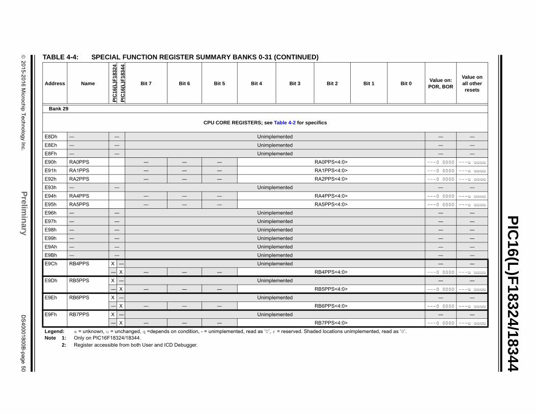
2
01
5-2
01
6 M
icroch
ip T
ech
no
log
y Inc.
Prelim
inary
DS
40
00
18
00
B-p
ag
e 5
0
PIC
16(L)F
18324/18344
E8 ― ―
E8 ― ―
E8 ― ―
E9 ---0 0000 ---u uuuu
E9 ---0 0000 ---u uuuu
E9 ---0 0000 ---u uuuu
E9 ― ―
E9 ---0 0000 ---u uuuu
E9 ---0 0000 ---u uuuu
E9 ― ―
E9 ― ―
E9 ― ―
E9 ― ―
E9 ― ―
E9 ― ―
E9 ― ―
---0 0000 ---u uuuu
E9 ― ―
---0 0000 ---u uuuu
E9 ― ―
---0 0000 ---u uuuu
E9 ― ―
---0 0000 ---u uuuu
TA
Ad Bit 0Value on:POR, BOR
Value on all other resets
Le , read as ‘0’.No
Bank 29
CPU CORE REGISTERS; see Table 4-2 for specifics
Dh ― ― Unimplemented
Eh ― ― Unimplemented
Fh ― ― Unimplemented
0h RA0PPS ― ― ― RA0PPS<4:0>
1h RA1PPS ― ― ― RA1PPS<4:0>
2h RA2PPS ― ― ― RA2PPS<4:0>
3h ― ― Unimplemented
4h RA4PPS ― ― ― RA4PPS<4:0>
5h RA5PPS ― ― ― RA5PPS<4:0>
6h ― ― Unimplemented
7h ― ― Unimplemented
8h ― ― Unimplemented
9h ― ― Unimplemented
Ah ― ― Unimplemented
Bh ― ― Unimplemented
Ch RB4PPS X ― Unimplemented
― X ― ― ― RB4PPS<4:0>
Dh RB5PPS X ― Unimplemented
― X ― ― ― RB5PPS<4:0>
Eh RB6PPS X ― Unimplemented
― X ― ― ― RB6PPS<4:0>
Fh RB7PPS X ― Unimplemented
― X ― ― ― RB7PPS<4:0>
BLE 4-4: SPECIAL FUNCTION REGISTER SUMMARY BANKS 0-31 (CONTINUED)
dress Name
PIC
16(L
)F1
832
4
PIC
16(L
)F1
834
4
Bit 7 Bit 6 Bit 5 Bit 4 Bit 3 Bit 2 Bit 1
gend: x = unknown, u = unchanged, q =depends on condition, - = unimplemented, read as ‘0’, r = reserved. Shaded locations unimplementedte 1: Only on PIC16F18324/18344.
2: Register accessible from both User and ICD Debugger.
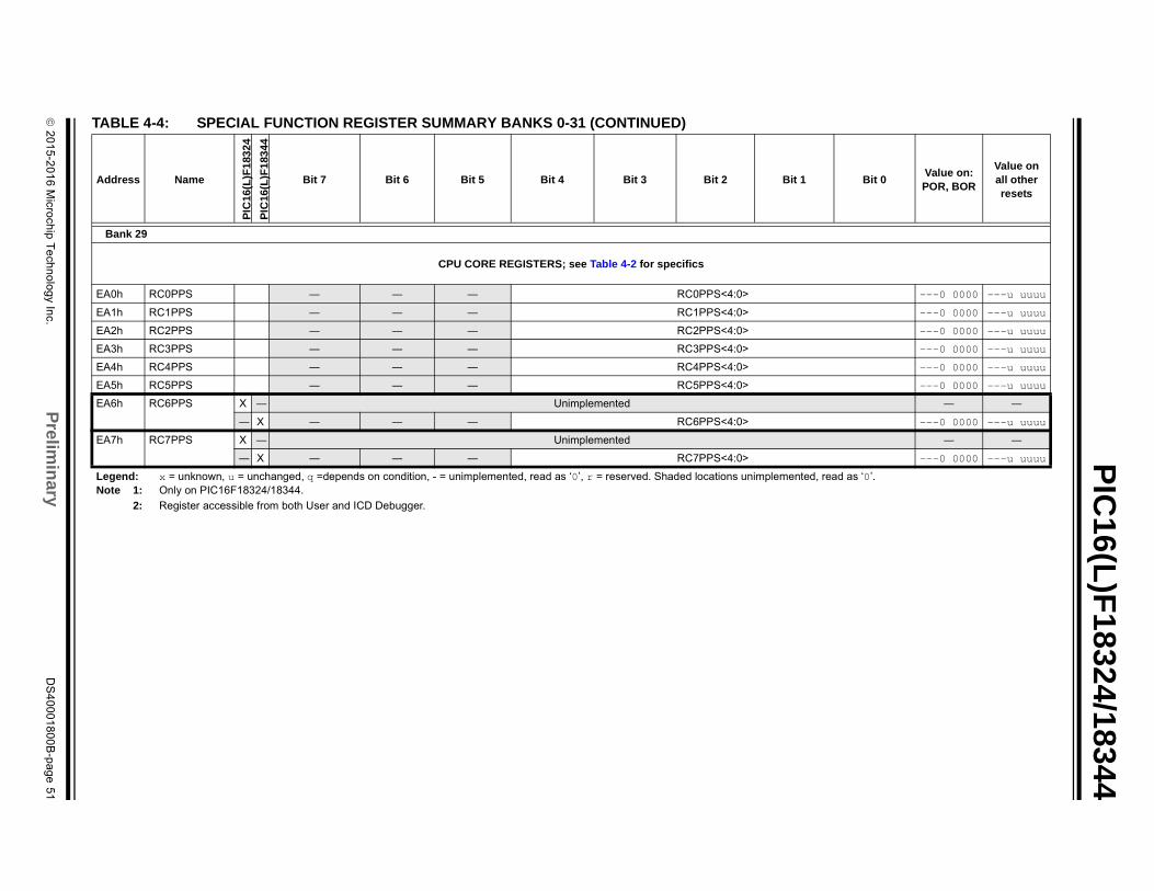
2
01
5-2
01
6 M
icroch
ip T
ech
no
log
y Inc.
Prelim
inary
DS
40
00
18
00
B-p
ag
e 5
1
PIC
16(L)F
18324/18344
EA ---0 0000 ---u uuuu
EA ---0 0000 ---u uuuu
EA ---0 0000 ---u uuuu
EA ---0 0000 ---u uuuu
EA ---0 0000 ---u uuuu
EA ---0 0000 ---u uuuu
EA ― ―
---0 0000 ---u uuuu
EA ― ―
---0 0000 ---u uuuu
TA
Ad Bit 0Value on:POR, BOR
Value on all other resets
Le , read as ‘0’.No
Bank 29
CPU CORE REGISTERS; see Table 4-2 for specifics
0h RC0PPS ― ― ― RC0PPS<4:0>
1h RC1PPS ― ― ― RC1PPS<4:0>
2h RC2PPS ― ― ― RC2PPS<4:0>
3h RC3PPS ― ― ― RC3PPS<4:0>
4h RC4PPS ― ― ― RC4PPS<4:0>
5h RC5PPS ― ― ― RC5PPS<4:0>
6h RC6PPS X ― Unimplemented
― X ― ― ― RC6PPS<4:0>
7h RC7PPS X ― Unimplemented
― X ― ― ― RC7PPS<4:0>
BLE 4-4: SPECIAL FUNCTION REGISTER SUMMARY BANKS 0-31 (CONTINUED)
dress Name
PIC
16(L
)F1
832
4
PIC
16(L
)F1
834
4
Bit 7 Bit 6 Bit 5 Bit 4 Bit 3 Bit 2 Bit 1
gend: x = unknown, u = unchanged, q =depends on condition, - = unimplemented, read as ‘0’, r = reserved. Shaded locations unimplementedte 1: Only on PIC16F18324/18344.
2: Register accessible from both User and ICD Debugger.
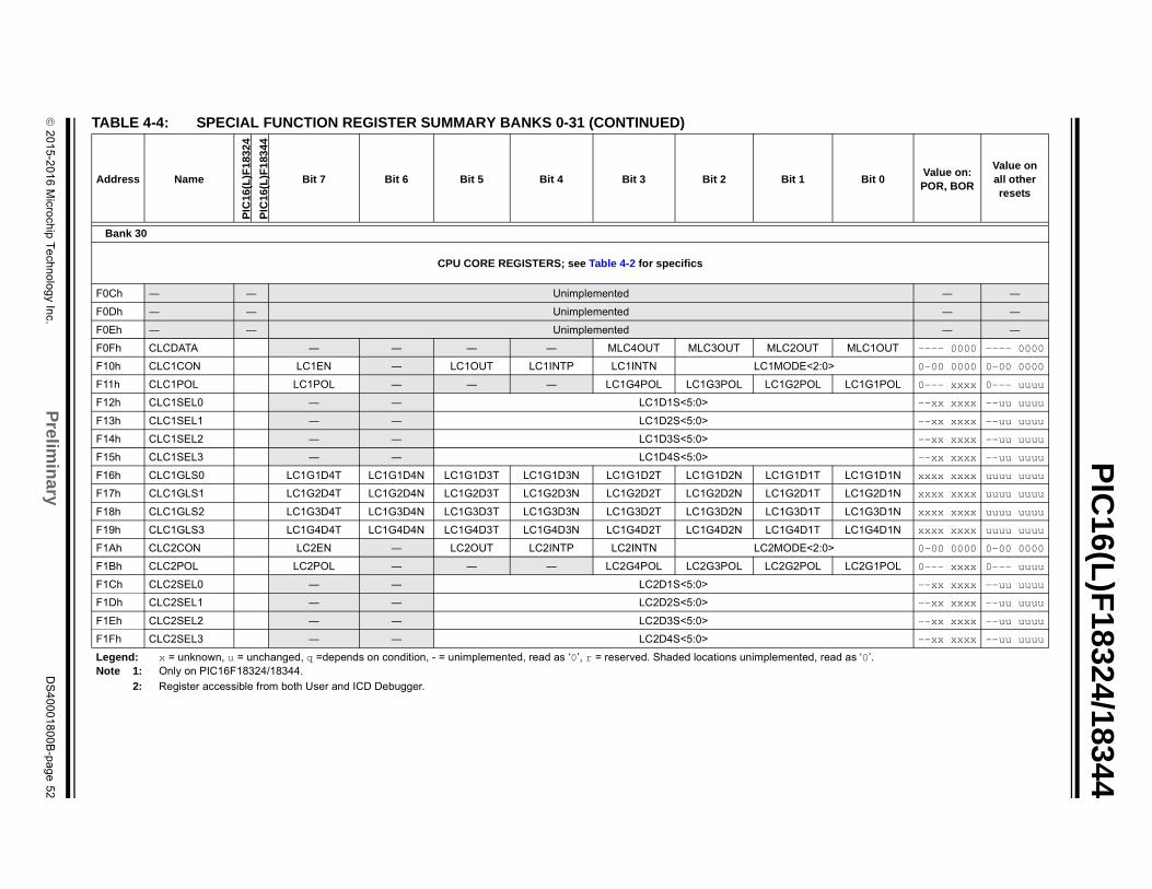
2
01
5-2
01
6 M
icroch
ip T
ech
no
log
y Inc.
Prelim
inary
DS
40
00
18
00
B-p
ag
e 5
2
PIC
16(L)F
18324/18344
F0 ― ―
F0 ― ―
F0 ― ―
F0 T MLC1OUT ---- 0000 ---- 0000
F1 2:0> 0-00 0000 0-00 0000
F1 L LC1G1POL 0--- xxxx 0--- uuuu
F1 --xx xxxx --uu uuuu
F1 --xx xxxx --uu uuuu
F1 --xx xxxx --uu uuuu
F1 --xx xxxx --uu uuuu
F1 T LC1G1D1N xxxx xxxx uuuu uuuu
F1 T LC1G2D1N xxxx xxxx uuuu uuuu
F1 T LC1G3D1N xxxx xxxx uuuu uuuu
F1 T LC1G4D1N xxxx xxxx uuuu uuuu
F1 2:0> 0-00 0000 0-00 0000
F1 L LC2G1POL 0--- xxxx 0--- uuuu
F1 --xx xxxx --uu uuuu
F1 --xx xxxx --uu uuuu
F1 --xx xxxx --uu uuuu
F1 --xx xxxx --uu uuuu
TA
Ad Bit 0Value on:POR, BOR
Value on all other resets
Le , read as ‘0’.No
Bank 30
CPU CORE REGISTERS; see Table 4-2 for specifics
Ch ― ― Unimplemented
Dh ― ― Unimplemented
Eh ― ― Unimplemented
Fh CLCDATA ― ― ― ― MLC4OUT MLC3OUT MLC2OU
0h CLC1CON LC1EN ― LC1OUT LC1INTP LC1INTN LC1MODE<
1h CLC1POL LC1POL ― ― ― LC1G4POL LC1G3POL LC1G2PO
2h CLC1SEL0 ― ― LC1D1S<5:0>
3h CLC1SEL1 ― ― LC1D2S<5:0>
4h CLC1SEL2 ― ― LC1D3S<5:0>
5h CLC1SEL3 ― ― LC1D4S<5:0>
6h CLC1GLS0 LC1G1D4T LC1G1D4N LC1G1D3T LC1G1D3N LC1G1D2T LC1G1D2N LC1G1D1
7h CLC1GLS1 LC1G2D4T LC1G2D4N LC1G2D3T LC1G2D3N LC1G2D2T LC1G2D2N LC1G2D1
8h CLC1GLS2 LC1G3D4T LC1G3D4N LC1G3D3T LC1G3D3N LC1G3D2T LC1G3D2N LC1G3D1
9h CLC1GLS3 LC1G4D4T LC1G4D4N LC1G4D3T LC1G4D3N LC1G4D2T LC1G4D2N LC1G4D1
Ah CLC2CON LC2EN ― LC2OUT LC2INTP LC2INTN LC2MODE<
Bh CLC2POL LC2POL ― ― ― LC2G4POL LC2G3POL LC2G2PO
Ch CLC2SEL0 ― ― LC2D1S<5:0>
Dh CLC2SEL1 ― ― LC2D2S<5:0>
Eh CLC2SEL2 ― ― LC2D3S<5:0>
Fh CLC2SEL3 ― ― LC2D4S<5:0>
BLE 4-4: SPECIAL FUNCTION REGISTER SUMMARY BANKS 0-31 (CONTINUED)
dress Name
PIC
16(L
)F1
832
4
PIC
16(L
)F1
834
4
Bit 7 Bit 6 Bit 5 Bit 4 Bit 3 Bit 2 Bit 1
gend: x = unknown, u = unchanged, q =depends on condition, - = unimplemented, read as ‘0’, r = reserved. Shaded locations unimplementedte 1: Only on PIC16F18324/18344.
2: Register accessible from both User and ICD Debugger.
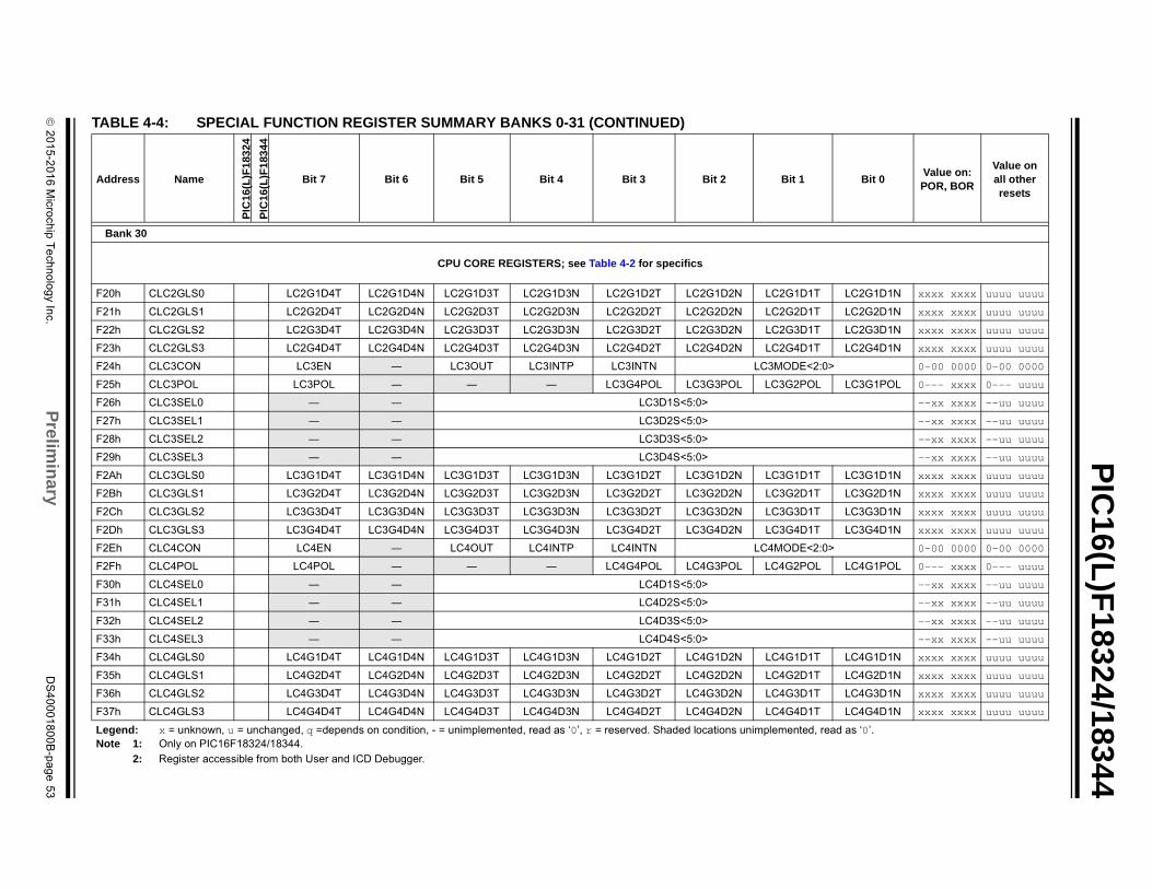
2
01
5-2
01
6 M
icroch
ip T
ech
no
log
y Inc.
Prelim
inary
DS
40
00
18
00
B-p
ag
e 5
3
PIC
16(L)F
18324/18344
F2 T LC2G1D1N xxxx xxxx uuuu uuuu
F2 T LC2G2D1N xxxx xxxx uuuu uuuu
F2 T LC2G3D1N xxxx xxxx uuuu uuuu
F2 T LC2G4D1N xxxx xxxx uuuu uuuu
F2 2:0> 0-00 0000 0-00 0000
F2 L LC3G1POL 0--- xxxx 0--- uuuu
F2 --xx xxxx --uu uuuu
F2 --xx xxxx --uu uuuu
F2 --xx xxxx --uu uuuu
F2 --xx xxxx --uu uuuu
F2 T LC3G1D1N xxxx xxxx uuuu uuuu
F2 T LC3G2D1N xxxx xxxx uuuu uuuu
F2 T LC3G3D1N xxxx xxxx uuuu uuuu
F2 T LC3G4D1N xxxx xxxx uuuu uuuu
F2 2:0> 0-00 0000 0-00 0000
F2 L LC4G1POL 0--- xxxx 0--- uuuu
F3 --xx xxxx --uu uuuu
F3 --xx xxxx --uu uuuu
F3 --xx xxxx --uu uuuu
F3 --xx xxxx --uu uuuu
F3 T LC4G1D1N xxxx xxxx uuuu uuuu
F3 T LC4G2D1N xxxx xxxx uuuu uuuu
F3 T LC4G3D1N xxxx xxxx uuuu uuuu
F3 T LC4G4D1N xxxx xxxx uuuu uuuu
TA
Ad Bit 0Value on:POR, BOR
Value on all other resets
Le , read as ‘0’.No
Bank 30
CPU CORE REGISTERS; see Table 4-2 for specifics
0h CLC2GLS0 LC2G1D4T LC2G1D4N LC2G1D3T LC2G1D3N LC2G1D2T LC2G1D2N LC2G1D1
1h CLC2GLS1 LC2G2D4T LC2G2D4N LC2G2D3T LC2G2D3N LC2G2D2T LC2G2D2N LC2G2D1
2h CLC2GLS2 LC2G3D4T LC2G3D4N LC2G3D3T LC2G3D3N LC2G3D2T LC2G3D2N LC2G3D1
3h CLC2GLS3 LC2G4D4T LC2G4D4N LC2G4D3T LC2G4D3N LC2G4D2T LC2G4D2N LC2G4D1
4h CLC3CON LC3EN ― LC3OUT LC3INTP LC3INTN LC3MODE<
5h CLC3POL LC3POL ― ― ― LC3G4POL LC3G3POL LC3G2PO
6h CLC3SEL0 ― ― LC3D1S<5:0>
7h CLC3SEL1 ― ― LC3D2S<5:0>
8h CLC3SEL2 ― ― LC3D3S<5:0>
9h CLC3SEL3 ― ― LC3D4S<5:0>
Ah CLC3GLS0 LC3G1D4T LC3G1D4N LC3G1D3T LC3G1D3N LC3G1D2T LC3G1D2N LC3G1D1
Bh CLC3GLS1 LC3G2D4T LC3G2D4N LC3G2D3T LC3G2D3N LC3G2D2T LC3G2D2N LC3G2D1
Ch CLC3GLS2 LC3G3D4T LC3G3D4N LC3G3D3T LC3G3D3N LC3G3D2T LC3G3D2N LC3G3D1
Dh CLC3GLS3 LC3G4D4T LC3G4D4N LC3G4D3T LC3G4D3N LC3G4D2T LC3G4D2N LC3G4D1
Eh CLC4CON LC4EN ― LC4OUT LC4INTP LC4INTN LC4MODE<
Fh CLC4POL LC4POL ― ― ― LC4G4POL LC4G3POL LC4G2PO
0h CLC4SEL0 ― ― LC4D1S<5:0>
1h CLC4SEL1 ― ― LC4D2S<5:0>
2h CLC4SEL2 ― ― LC4D3S<5:0>
3h CLC4SEL3 ― ― LC4D4S<5:0>
4h CLC4GLS0 LC4G1D4T LC4G1D4N LC4G1D3T LC4G1D3N LC4G1D2T LC4G1D2N LC4G1D1
5h CLC4GLS1 LC4G2D4T LC4G2D4N LC4G2D3T LC4G2D3N LC4G2D2T LC4G2D2N LC4G2D1
6h CLC4GLS2 LC4G3D4T LC4G3D4N LC4G3D3T LC4G3D3N LC4G3D2T LC4G3D2N LC4G3D1
7h CLC4GLS3 LC4G4D4T LC4G4D4N LC4G4D3T LC4G4D3N LC4G4D2T LC4G4D2N LC4G4D1
BLE 4-4: SPECIAL FUNCTION REGISTER SUMMARY BANKS 0-31 (CONTINUED)
dress Name
PIC
16(L
)F1
832
4
PIC
16(L
)F1
834
4
Bit 7 Bit 6 Bit 5 Bit 4 Bit 3 Bit 2 Bit 1
gend: x = unknown, u = unchanged, q =depends on condition, - = unimplemented, read as ‘0’, r = reserved. Shaded locations unimplementedte 1: Only on PIC16F18324/18344.
2: Register accessible from both User and ICD Debugger.
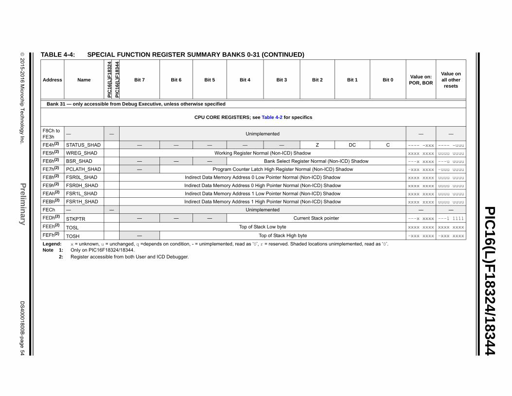
2
01
5-2
01
6 M
icroch
ip T
ech
no
log
y Inc.
Prelim
inary
DS
40
00
18
00
B-p
ag
e 5
4
PIC
16(L)F
18324/18344
F8FE
— —
FE C ---- -xxx ---- -uuu
FE xxxx xxxx uuuu uuuu
FE ow ---x xxxx ---u uuuu
FE -xxx xxxx -uuu uuuu
FE xxxx xxxx uuuu uuuu
FE xxxx xxxx uuuu uuuu
FE xxxx xxxx uuuu uuuu
FE xxxx xxxx uuuu uuuu
FE — —
FE ---x xxxx ---1 1111
FE xxxx xxxx xxxx xxxx
FE -xxx xxxx -xxx xxxx
TA
Ad Bit 0Value on:POR, BOR
Value on all other resets
Le , read as ‘0’.No
Bank 31 — only accessible from Debug Executive, unless otherwise specified
CPU CORE REGISTERS; see Table 4-2 for specifics
Ch to 3h
— ― Unimplemented
4h(2) STATUS_SHAD — — — — — Z DC
5h(2) WREG_SHAD Working Register Normal (Non-ICD) Shadow
6h(2) BSR_SHAD — — — Bank Select Register Normal (Non-ICD) Shad
7h(2) PCLATH_SHAD — Program Counter Latch High Register Normal (Non-ICD) Shadow
8h(2) FSR0L_SHAD Indirect Data Memory Address 0 Low Pointer Normal (Non-ICD) Shadow
9h(2) FSR0H_SHAD Indirect Data Memory Address 0 High Pointer Normal (Non-ICD) Shadow
Ah(2) FSR1L_SHAD Indirect Data Memory Address 1 Low Pointer Normal (Non-ICD) Shadow
Bh(2) FSR1H_SHAD Indirect Data Memory Address 1 High Pointer Normal (Non-ICD) Shadow
Ch — ― Unimplemented
Dh(2)STKPTR — — — Current Stack pointer
Eh(2)TOSL Top of Stack Low byte
Fh(2)TOSH — Top of Stack High byte
BLE 4-4: SPECIAL FUNCTION REGISTER SUMMARY BANKS 0-31 (CONTINUED)
dress Name
PIC
16(L
)F1
832
4
PIC
16(L
)F1
834
4
Bit 7 Bit 6 Bit 5 Bit 4 Bit 3 Bit 2 Bit 1
gend: x = unknown, u = unchanged, q =depends on condition, - = unimplemented, read as ‘0’, r = reserved. Shaded locations unimplementedte 1: Only on PIC16F18324/18344.
2: Register accessible from both User and ICD Debugger.
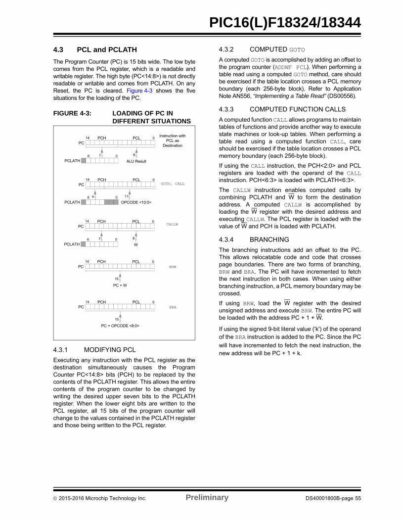
PIC16(L)F18324/18344
4.3 PCL and PCLATH
The Program Counter (PC) is 15 bits wide. The low bytecomes from the PCL register, which is a readable andwritable register. The high byte (PC<14:8>) is not directlyreadable or writable and comes from PCLATH. On anyReset, the PC is cleared. Figure 4-3 shows the fivesituations for the loading of the PC.
FIGURE 4-3: LOADING OF PC IN DIFFERENT SITUATIONS
4.3.1 MODIFYING PCL
Executing any instruction with the PCL register as thedestination simultaneously causes the ProgramCounter PC<14:8> bits (PCH) to be replaced by thecontents of the PCLATH register. This allows the entirecontents of the program counter to be changed bywriting the desired upper seven bits to the PCLATHregister. When the lower eight bits are written to thePCL register, all 15 bits of the program counter willchange to the values contained in the PCLATH registerand those being written to the PCL register.
4.3.2 COMPUTED GOTO
A computed GOTO is accomplished by adding an offset tothe program counter (ADDWF PCL). When performing atable read using a computed GOTO method, care shouldbe exercised if the table location crosses a PCL memoryboundary (each 256-byte block). Refer to ApplicationNote AN556, “Implementing a Table Read” (DS00556).
4.3.3 COMPUTED FUNCTION CALLS
A computed function CALL allows programs to maintaintables of functions and provide another way to executestate machines or look-up tables. When performing atable read using a computed function CALL, careshould be exercised if the table location crosses a PCLmemory boundary (each 256-byte block).
If using the CALL instruction, the PCH<2:0> and PCLregisters are loaded with the operand of the CALLinstruction. PCH<6:3> is loaded with PCLATH<6:3>.
The CALLW instruction enables computed calls bycombining PCLATH and W to form the destinationaddress. A computed CALLW is accomplished byloading the W register with the desired address andexecuting CALLW. The PCL register is loaded with thevalue of W and PCH is loaded with PCLATH.
4.3.4 BRANCHING
The branching instructions add an offset to the PC.This allows relocatable code and code that crossespage boundaries. There are two forms of branching,BRW and BRA. The PC will have incremented to fetchthe next instruction in both cases. When using eitherbranching instruction, a PCL memory boundary may becrossed.
If using BRW, load the W register with the desiredunsigned address and execute BRW. The entire PC willbe loaded with the address PC + 1 + W.
If using the signed 9-bit literal value ('k') of the operandof the BRA instruction is added to the PC. Since the PC
will have incremented to fetch the next instruction, thenew address will be PC + 1 + k.
PCLPCH 014
PC
PCLPCH 014
PC
ALU Result
876
PCLATH0
Instruction withPCL as
Destination
GOTO, CALL
OPCODE <10:0>
1146
PCLATH0
PCLPCH 014
PC
W
876
PCLATH0
CALLW
PCLPCH 014
PC
PC + W
15
BRW
PCLPCH 014
PC
PC + OPCODE <8:0>
15
BRA
2015-2016 Microchip Technology Inc. Preliminary DS40001800B-page 55
PIC16(L)F18324/18344
4.4 Stack
All devices have a 16-level x 15-bit wide hardwarestack (refer to Figure 4-4 through Figure 4-7). Thestack space is not part of either program or data space.The PC is PUSHed onto the stack when CALL orCALLW instructions are executed or an interrupt causesa branch. The stack is POPed in the event of aRETURN, RETLW or a RETFIE instruction execution.PCLATH is not affected by a PUSH or POP operation.
The stack operates as a circular buffer and does notcause a Reset when either a Stack Overflow orUnderflow occur if the STVREN bit is programmed to‘0‘ (Configuration Words). This means that after thestack has been PUSHed sixteen times, theseventeenth PUSH overwrites the value that wasstored from the first PUSH. The eighteenth PUSHoverwrites the second PUSH (and so on). TheSTKOVF and STKUNF flag bits will be set on anOverflow/Underflow, regardless of whether the Reset isenabled.
If the STVREN bit in Configuration Words isprogrammed to ‘1’, the device will be Reset if the stackis PUSHed beyond the sixteenth level or POPedbeyond the first level, setting the appropriate bits(STKOVF or STKUNF, respectively) in the PCONregister.
4.4.1 ACCESSING THE STACK
The stack is accessible through the TOSH, TOSL andSTKPTR registers. STKPTR is the current value of theStack Pointer. TOSH:TOSL register pair points to theTOP of the stack. Both registers are read/writable. TOSis split into TOSH and TOSL due to the 15-bit size of thePC. To access the stack, adjust the value of STKPTR,which will position TOSH:TOSL, then read/write toTOSH:TOSL. STKPTR is five bits to allow detection ofoverflow and underflow.
During normal program operation, CALL, CALLW andInterrupts will increment STKPTR while RETLW,RETURN, and RETFIE will decrement STKPTR. At anytime, STKPTR can be read to see how many levelsremain available on the stack. The STKPTR alwayspoints at the currently used place on the stack.Therefore, a CALL or CALLW will increment theSTKPTR and then write the PC, and a return will writethe PC and then decrement the STKPTR.
Reference Figure 4-4 through Figure 4-7 for examplesof accessing the stack.
Note 1: There are no instructions/mnemonicscalled PUSH or POP. These are actionsthat occur from the execution of theCALL, CALLW, RETURN, RETLW andRETFIE instructions or the vectoring toan interrupt address.
Note: Care should be taken when modifying theSTKPTR while interrupts are enabled.
2015-2016 Microchip Technology Inc. Preliminary DS40001800B-page 56
PIC16(L)F18324/18344
FIGURE 4-4: ACCESSING THE STACK EXAMPLE 1
FIGURE 4-5: ACCESSING THE STACK EXAMPLE 2
0x0F
0x0E
0x0D
0x0C
0x0B
0x0A
0x09
0x08
0x07
0x06
0x05
0x04
0x03
0x02
0x01
0x00
0x0000
STKPTR = 0x1F
Initial Stack Configuration:
After Reset, the stack is empty. Theempty stack is initialized so the StackPointer is pointing at 0x1F-1. If the StackOverflow/Underflow Reset is enabled, theTOSH/TOSL registers will return ‘0’. Ifthe Stack Overflow/Underflow Reset isdisabled, the TOSH/TOSL registers willreturn the contents of stack address 0x0F.
0x1F STKPTR = 0x1F
Stack Reset Disabled(STVREN = 0)
Stack Reset Enabled(STVREN = 1)
TOSH:TOSL
TOSH:TOSL
0x0F
0x0E
0x0D
0x0C
0x0B
0x0A
0x09
0x08
0x07
0x06
0x05
0x04
0x03
0x02
0x01
Return Address0x00 STKPTR = 0x00
This figure shows the stack configurationafter the first CALL or a single interrupt.If a RETURN instruction is executed, thereturn address will be placed in theProgram Counter and the Stack Pointerdecremented to the empty state (0x1F).
TOSH:TOSL
2015-2016 Microchip Technology Inc. Preliminary DS40001800B-page 57
PIC16(L)F18324/18344
FIGURE 4-6: ACCESSING THE STACK EXAMPLE 3
FIGURE 4-7: ACCESSING THE STACK EXAMPLE 4
0x0F
0x0E
0x0D
0x0C
0x0B
0x0A
0x09
0x08
0x07
Return Address0x06
Return Address0x05
Return Address0x04
Return Address0x03
Return Address0x02
Return Address0x01
Return Address0x00
STKPTR = 0x06
After seven CALLs or six CALLs and aninterrupt, the stack looks like the figureon the left. A series of RETURN instructionswill repeatedly place the return addresses into the Program Counter and pop the stack.
TOSH:TOSL
0x0F
0x0E
0x0D
0x0C
0x0B
0x0A
0x09
0x08
0x07
0x06
0x05
0x04
0x03
0x02
0x01
Return Address0x00 STKPTR = 0x10
When the stack is full, the next CALL oran interrupt will set the Stack Pointer to0x10. This is identical to address 0x00so the stack will wrap and overwrite thereturn address at 0x00. If the StackOverflow/Underflow Reset is enabled, aReset will occur and location 0x00 willnot be overwritten.
Return Address
Return Address
Return Address
Return Address
Return Address
Return Address
Return Address
Return Address
Return Address
Return Address
Return Address
Return Address
Return Address
Return Address
Return Address
TOSH:TOSL
2015-2016 Microchip Technology Inc. Preliminary DS40001800B-page 58
PIC16(L)F18324/18344
4.5 Indirect Addressing
The INDFn registers are not physical registers. Anyinstruction that accesses an INDFn register actuallyaccesses the register at the address specified by theFile Select Registers (FSR). If the FSRn addressspecifies one of the two INDFn registers, the read willreturn ‘0’ and the write will not occur (though Status bitsmay be affected). The FSRn register value is createdby the pair FSRnH and FSRnL.
The FSR registers form a 16-bit address that allows anaddressing space with 65536 locations. These locationsare divided into four memory regions:
• Banked Data Memory• Linear Data Memory• Program Flash Memory• EEPROM
4.5.1 BANKED DATA MEMORY
The traditional data memory is a region from FSRaddress 0x000 to FSR address 0xFFF. The addressescorrespond to the absolute addresses of all SFR, GPRand common registers.
FIGURE 4-8: BANKED DATA MEMORY MAP
Indirect AddressingDirect Addressing
Bank Select Location Select
4 BSR 6 0From Opcode FSRxL7 0
Bank Select Location Select
00000 00001 00010 111110x00
0x7F
Bank 0 Bank 1 Bank 2 Bank 31
0 FSRxH7 0
0 0 0 0
2015-2016 Microchip Technology Inc. Preliminary DS40001800B-page 59
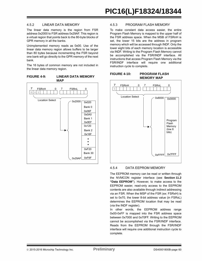
PIC16(L)F18324/18344
4.5.2 LINEAR DATA MEMORY
The linear data memory is the region from FSRaddress 0x2000 to FSR address 0x29AF. This region isa virtual region that points back to the 80-byte blocks ofGPR memory in all the banks.
Unimplemented memory reads as 0x00. Use of thelinear data memory region allows buffers to be largerthan 80 bytes because incrementing the FSR beyondone bank will go directly to the GPR memory of the nextbank.
The 16 bytes of common memory are not included inthe linear data memory region.
FIGURE 4-9: LINEAR DATA MEMORY MAP
4.5.3 PROGRAM FLASH MEMORY
To make constant data access easier, the entireProgram Flash Memory is mapped to the upper half ofthe FSR address space. When the MSB of FSRnH isset, the lower 15 bits are the address in programmemory which will be accessed through INDF. Only thelower eight bits of each memory location is accessiblevia INDF. Writing to the Program Flash Memory cannotbe accomplished via the FSR/INDF interface. Allinstructions that access Program Flash Memory via theFSR/INDF interface will require one additionalinstruction cycle to complete.
FIGURE 4-10: PROGRAM FLASH MEMORY MAP
4.5.4 DATA EEPROM MEMORY
The EEPROM memory can be read or written throughthe NVMCON register interface (see Section 11.2“Data EEPROM”). However, to make access to theEEPROM easier, read-only access to the EEPROMcontents are also available through indirect addressingvia an FSR. When the MSP of the FSR (ex: FSRxH) isset to 0x70, the lower 8-bit address value (in FSRxL)determines the EEPROM location that may be read(via the INDF register). In other words, the EEPROM address range0x00-0xFF is mapped into the FSR address spacebetween 0x7000 and 0x70FF. Writing to the EEPROMcannot be accomplished via the FSR/INDF interface.Reads from the EEPROM through the FSR/INDFinterface will require one additional instruction cycle tocomplete.
7
0 170 0
Location Select 0x2000
FSRnH FSRnL
0x020
Bank 0
0x06F0x0A0
Bank 1
0x0EF
0x120
Bank 2
0x16F
0xF20
Bank 30
0xF6F0x29AF
0
7
170 0
Location Select 0x8000
FSRnH FSRnL
0x0000
0x7FFF0xFFFF
ProgramFlashMemory(low 8bits)
2015-2016 Microchip Technology Inc. Preliminary DS40001800B-page 60
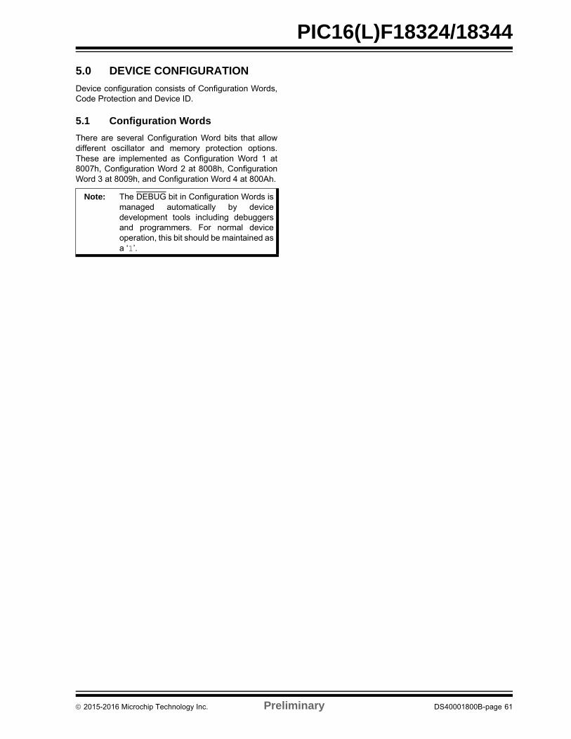
PIC16(L)F18324/18344
5.0 DEVICE CONFIGURATION
Device configuration consists of Configuration Words,Code Protection and Device ID.
5.1 Configuration Words
There are several Configuration Word bits that allowdifferent oscillator and memory protection options.These are implemented as Configuration Word 1 at8007h, Configuration Word 2 at 8008h, ConfigurationWord 3 at 8009h, and Configuration Word 4 at 800Ah.
Note: The DEBUG bit in Configuration Words ismanaged automatically by devicedevelopment tools including debuggersand programmers. For normal deviceoperation, this bit should be maintained asa ‘1’.
2015-2016 Microchip Technology Inc. Preliminary DS40001800B-page 61
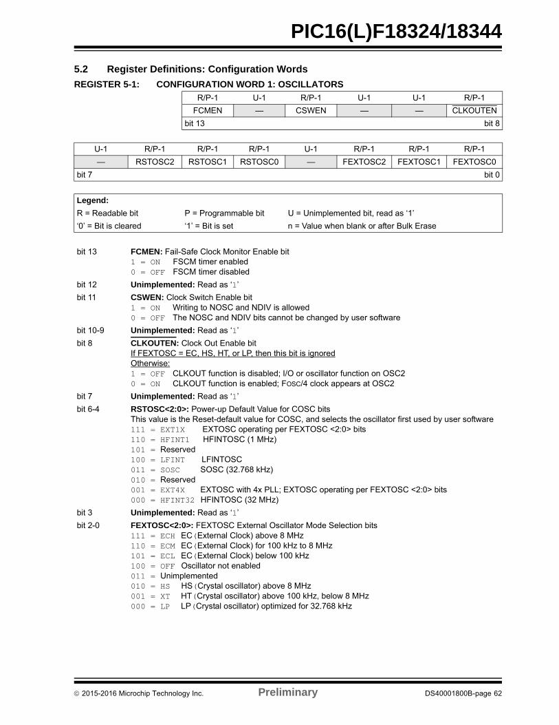
PIC16(L)F18324/18344
5.2 Register Definitions: Configuration Words
REGISTER 5-1: CONFIGURATION WORD 1: OSCILLATORS
R/P-1 U-1 R/P-1 U-1 U-1 R/P-1
FCMEN — CSWEN — — CLKOUTEN
bit 13 bit 8
U-1 R/P-1 R/P-1 R/P-1 U-1 R/P-1 R/P-1 R/P-1
— RSTOSC2 RSTOSC1 RSTOSC0 — FEXTOSC2 FEXTOSC1 FEXTOSC0
bit 7 bit 0
Legend:
R = Readable bit P = Programmable bit U = Unimplemented bit, read as ‘1’
‘0’ = Bit is cleared ‘1’ = Bit is set n = Value when blank or after Bulk Erase
bit 13 FCMEN: Fail-Safe Clock Monitor Enable bit1 = ON FSCM timer enabled0 = OFF FSCM timer disabled
bit 12 Unimplemented: Read as ‘1’
bit 11 CSWEN: Clock Switch Enable bit1 = ON Writing to NOSC and NDIV is allowed0 = OFF The NOSC and NDIV bits cannot be changed by user software
bit 10-9 Unimplemented: Read as ‘1’
bit 8 CLKOUTEN: Clock Out Enable bitIf FEXTOSC = EC, HS, HT, or LP, then this bit is ignoredOtherwise: 1 = OFF CLKOUT function is disabled; I/O or oscillator function on OSC20 = ON CLKOUT function is enabled; FOSC/4 clock appears at OSC2
bit 7 Unimplemented: Read as ‘1’
bit 6-4 RSTOSC<2:0>: Power-up Default Value for COSC bitsThis value is the Reset-default value for COSC, and selects the oscillator first used by user software 111 = EXT1X EXTOSC operating per FEXTOSC <2:0> bits 110 = HFINT1 HFINTOSC (1 MHz)101 = Reserved100 = LFINT LFINTOSC011 = SOSC SOSC (32.768 kHz)010 = Reserved001 = EXT4X EXTOSC with 4x PLL; EXTOSC operating per FEXTOSC <2:0> bits000 = HFINT32 HFINTOSC (32 MHz)
bit 3 Unimplemented: Read as ‘1’
bit 2-0 FEXTOSC<2:0>: FEXTOSC External Oscillator Mode Selection bits111 = ECH EC(External Clock) above 8 MHz110 = ECM EC(External Clock) for 100 kHz to 8 MHz101 = ECL EC(External Clock) below 100 kHz100 = OFF Oscillator not enabled011 = Unimplemented010 = HS HS(Crystal oscillator) above 8 MHz 001 = XT HT(Crystal oscillator) above 100 kHz, below 8 MHz 000 = LP LP(Crystal oscillator) optimized for 32.768 kHz
2015-2016 Microchip Technology Inc. Preliminary DS40001800B-page 62
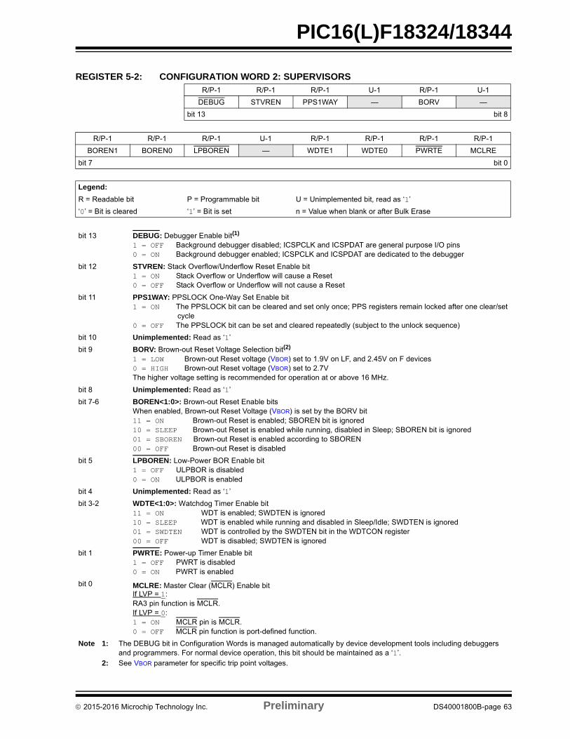
PIC16(L)F18324/18344
REGISTER 5-2: CONFIGURATION WORD 2: SUPERVISORS
R/P-1 R/P-1 R/P-1 U-1 R/P-1 U-1
DEBUG STVREN PPS1WAY — BORV —
bit 13 bit 8
R/P-1 R/P-1 R/P-1 U-1 R/P-1 R/P-1 R/P-1 R/P-1
BOREN1 BOREN0 LPBOREN — WDTE1 WDTE0 PWRTE MCLRE
bit 7 bit 0
Legend:
R = Readable bit P = Programmable bit U = Unimplemented bit, read as ‘1’
‘0’ = Bit is cleared ‘1’ = Bit is set n = Value when blank or after Bulk Erase
bit 13 DEBUG: Debugger Enable bit(1)
1 = OFF Background debugger disabled; ICSPCLK and ICSPDAT are general purpose I/O pins0 = ON Background debugger enabled; ICSPCLK and ICSPDAT are dedicated to the debugger
bit 12 STVREN: Stack Overflow/Underflow Reset Enable bit1 = ON Stack Overflow or Underflow will cause a Reset0 = OFF Stack Overflow or Underflow will not cause a Reset
bit 11 PPS1WAY: PPSLOCK One-Way Set Enable bit1 = ON The PPSLOCK bit can be cleared and set only once; PPS registers remain locked after one clear/set
cycle0 = OFF The PPSLOCK bit can be set and cleared repeatedly (subject to the unlock sequence)
bit 10 Unimplemented: Read as ‘1’
bit 9 BORV: Brown-out Reset Voltage Selection bit(2)
1 = LOW Brown-out Reset voltage (VBOR) set to 1.9V on LF, and 2.45V on F devices0 = HIGH Brown-out Reset voltage (VBOR) set to 2.7VThe higher voltage setting is recommended for operation at or above 16 MHz.
bit 8 Unimplemented: Read as ‘1’
bit 7-6 BOREN<1:0>: Brown-out Reset Enable bitsWhen enabled, Brown-out Reset Voltage (VBOR) is set by the BORV bit11 = ON Brown-out Reset is enabled; SBOREN bit is ignored10 = SLEEP Brown-out Reset is enabled while running, disabled in Sleep; SBOREN bit is ignored01 = SBOREN Brown-out Reset is enabled according to SBOREN00 = OFF Brown-out Reset is disabled
bit 5 LPBOREN: Low-Power BOR Enable bit1 = OFF ULPBOR is disabled0 = ON ULPBOR is enabled
bit 4 Unimplemented: Read as ‘1’
bit 3-2 WDTE<1:0>: Watchdog Timer Enable bit11 = ON WDT is enabled; SWDTEN is ignored10 = SLEEP WDT is enabled while running and disabled in Sleep/Idle; SWDTEN is ignored01 = SWDTEN WDT is controlled by the SWDTEN bit in the WDTCON register00 = OFF WDT is disabled; SWDTEN is ignored
bit 1 PWRTE: Power-up Timer Enable bit1 = OFF PWRT is disabled0 = ON PWRT is enabled
bit 0 MCLRE: Master Clear (MCLR) Enable bitIf LVP = 1:RA3 pin function is MCLR.If LVP = 0:1 = ON MCLR pin is MCLR.0 = OFF MCLR pin function is port-defined function.
Note 1: The DEBUG bit in Configuration Words is managed automatically by device development tools including debuggers and programmers. For normal device operation, this bit should be maintained as a ‘1’.
2: See VBOR parameter for specific trip point voltages.
2015-2016 Microchip Technology Inc. Preliminary DS40001800B-page 63
PIC16(L)F18324/18344
REGISTER 5-3: CONFIGURATION WORD 3: MEMORY
R/P-1 U-1 U-1 U-1 U-1 U-1
LVP(1) — — — — —
bit 13 bit 8
U-1 U-1 U-1 U-1 U-1 U-1 R/P-1 R/P-1
— — — — — — WRT1 WRT0
bit 7 bit 0
Legend:
R = Readable bit P = Programmable bit U = Unimplemented bit, read as ‘1’
‘0’ = Bit is cleared ‘1’ = Bit is set n = Value when blank or after Bulk Erase
bit 13 LVP: Low-Voltage Programming Enable bit(1)
1 = ON Low-Voltage Programming is enabled. MCLR/VPP pin function is MCLR. MCLREConfiguration bit is ignored.
0 = OFF HV on MCLR/VPP must be used for programming.
bit 12-2 Unimplemented: Read as ‘1’
bit 1-0 WRT<1:0>: User NVM Self-Write Protection bits11 = OFF Write protection off10 = BOOT 0000h to 01FFh write-protected, 0200h to 0FFFh may be modified01 = HALF 0000h to 07FFh write-protected, 0800h to 0FFFh may be modified00 = ALL 0000h to 0FFFh write-protected, no addresses may be modifiedWRT applies only to the self-write feature of the device; writing through ICSP is never protected.
Note 1: The LVP bit cannot be programmed to ‘0’ when programming mode is entered via LVP.
2015-2016 Microchip Technology Inc. Preliminary DS40001800B-page 64
PIC16(L)F18324/18344
REGISTER 5-4: CONFIGURATION WORD 4: CODE PROTECTION
U-1 U-1 U-1 U-1 U-1 U-1
— — — — — —
bit 13 bit 8
U-1 U-1 U-1 U-1 U-1 U-1 R/P-1 R/P-1
— — — — — — CPD CP
bit 7 bit 0
Legend:
R = Readable bit P = Programmable bit U = Unimplemented bit, read as ‘1’
‘0’ = Bit is cleared ‘1’ = Bit is set n = Value when blank or after Bulk Erase
bit 13-2 Unimplemented: Read as ‘1’
bit 1 CPD: Data EEPROM Memory Code Protection bit1 = OFF Data EEPROM code protection disabled0 = ON Data EEPROM code protection enabled
bit 0 CP: Program Memory Code Protection bit1 = OFF Program memory code protection disabled0 = ON Program memory code protection enabled
2015-2016 Microchip Technology Inc. Preliminary DS40001800B-page 65
PIC16(L)F18324/18344
5.3 Code Protection
Code protection allows the device to be protected fromunauthorized access. Program memory protection anddata memory are controlled independently. Internalaccess to the program memory is unaffected by anycode protection setting.
5.3.1 PROGRAM MEMORY PROTECTION
The entire program memory space is protected fromexternal reads and writes by the CP bit in ConfigurationWords. When CP = 0, external reads and writes ofprogram memory are inhibited and a read will return all‘0’s. The CPU can continue to read program memory,regardless of the protection bit settings. Self-writewriting the program memory is dependent upon thewrite protection setting. See Section 5.4 “WriteProtection” for more information.
5.3.2 DATA MEMORY PROTECTION
The entire data EEPROM is protected from externalreads and writes by the CPD bit in the ConfigurationWords. When CPD = 0, external reads and writes ofEEPROM memory are inhibited and a read will returnall ‘0’s. The CPU can continue to read and writeEEPROM memory, regardless of the protection bitsettings.
5.4 Write Protection
Write protection allows the device to be protected fromunintended self-writes. Applications, such as bootloader software, can be protected while allowing otherregions of the program memory to be modified.
The WRT<1:0> bits in Configuration Words define thesize of the program memory block that is protected.
5.5 User ID
Four memory locations (8000h-8003h) are designatedas ID locations where the user can store checksum orother code identification numbers. These locations arereadable and writable during normal execution. SeeSection 11.4.7 “NVMREG EEPROM, User ID, DeviceID and Configuration Word Access” for moreinformation on accessing these memory locations. Formore information on checksum calculation, see the“PIC16(L)F183XX Memory ProgrammingSpecification” (DS40001738).
5.6 Device ID and Revision ID
The 14-bit device ID word is located at 8006h and the14-bit revision ID is located at 8005h. These locationsare read-only and cannot be erased or modified. SeeSection 11.4.7 “NVMREG EEPROM, User ID, DeviceID and Configuration Word Access” for moreinformation on accessing these memory locations.
Development tools, such as device programmers anddebuggers, may be used to read the Device ID andRevision ID.
2015-2016 Microchip Technology Inc. Preliminary DS40001800B-page 66
PIC16(L)F18324/18344
5.7 Register Definitions: Device and Revision
REGISTER 5-5: DEVID: DEVICE ID REGISTER
R R R R R R
DEV<13:8>
bit 13 bit 8
R R R R R R R R
DEV<7:0>
bit 7 bit 0
Legend:
R = Readable bit
‘1’ = Bit is set ‘0’ = Bit is cleared
bit 13-0 DEV<13:0>: Device ID bits
REGISTER 5-6: REVID: REVISION ID REGISTER
R-1 R-0 R R R R
REV<13:8>
bit 13 bit 8
R R R R R R R R
REV<7:0>
bit 7 bit 0
Legend:
R = Readable bit
‘1’ = Bit is set ‘0’ = Bit is cleared
bit 13-0 REV<13:0>: Revision ID bits
Note: The upper two bits of the Revision ID register will always read ‘10’.
Device DEVID<13:0> Values
PIC16F18324 11 0000 0011 1010 (303Ah)
PIC16LF18324 11 0000 0011 1100 (303Ch)
PIC16F18344 11 0000 0011 1011 (303Bh)
PIC16LF18344 11 0000 0011 1101 (303Dh)
2015-2016 Microchip Technology Inc. Preliminary DS40001800B-page 67
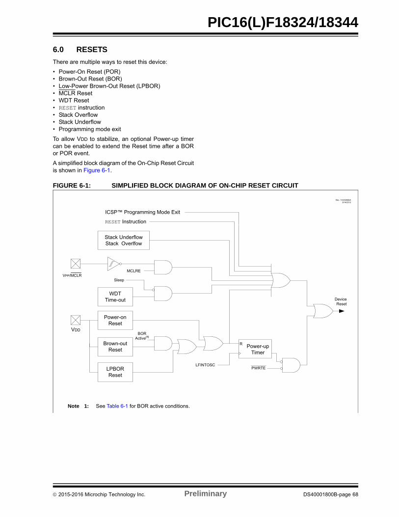
PIC16(L)F18324/18344
6.0 RESETS
There are multiple ways to reset this device:
• Power-On Reset (POR)• Brown-Out Reset (BOR)• Low-Power Brown-Out Reset (LPBOR)• MCLR Reset• WDT Reset• RESET instruction• Stack Overflow• Stack Underflow• Programming mode exit
To allow VDD to stabilize, an optional Power-up timercan be enabled to extend the Reset time after a BORor POR event.
A simplified block diagram of the On-Chip Reset Circuitis shown in Figure 6-1.
FIGURE 6-1: SIMPLIFIED BLOCK DIAGRAM OF ON-CHIP RESET CIRCUIT
Note 1: See Table 6-1 for BOR active conditions.
DeviceReset
Power-on Reset
WDT Time-out
Brown-out Reset
LPBOR Reset
RESET Instruction
MCLRE
Sleep
BOR Active(1)
PWRTELFINTOSC
VDD
ICSP™ Programming Mode Exit
Stack UnderflowStack Overlfow
VPP/MCLR
R Power-up Timer
Rev. 10-000006A8/14/2013
2015-2016 Microchip Technology Inc. Preliminary DS40001800B-page 68
PIC16(L)F18324/18344
6.1 Power-on Reset (POR)
The POR circuit holds the device in Reset until VDD hasreached an acceptable level for minimum operation.Slow rising VDD, fast operating speeds or analogperformance may require greater than minimum VDD.The PWRT, BOR or MCLR features can be used toextend the start-up period until all device operationconditions have been met.
6.2 Brown-out Reset (BOR)
The BOR circuit holds the device in Reset while VDD isbelow a selectable minimum level. Between the PORand BOR, complete voltage range coverage for execu-tion protection can be implemented.
The Brown-out Reset module has four operatingmodes controlled by the BOREN<1:0> bits inConfiguration Words. The four operating modes are:
• BOR is always on• BOR is off when in Sleep• BOR is controlled by software• BOR is always off
Refer to Table 6-1 for more information.
The Brown-out Reset voltage level is selectable byconfiguring the BORV bit in Configuration Words.
A VDD noise rejection filter prevents the BOR fromtriggering on small events. If VDD falls below VBOR fora duration greater than parameter TBORDC, the devicewill reset, and the BOR bit of the PCON0 register willbe cleared, indicating that a Brown-out Reset conditionoccurred. See Figure 6-2 for more information.
TABLE 6-1: BOR OPERATING MODES
BOREN<1:0> SBOREN Device Mode BOR ModeInstruction Execution upon:
Release of POR or Wake-up from Sleep
11 X X Active In these specific cases, “Release of POR” and “Wake-up from Sleep”, there is no delay in start-up. The BOR ready flag, (BORRDY = 1), will be set before the CPU is ready to execute instructions because the BOR circuit is forced on by the BOREN<1:0> bits.
10 XAwake Active Waits for release of BOR (BORRDY = 1)
Sleep Disabled BOR ignored when asleep
01
1
X
Active In these specific cases, “Release of POR” and “Wake-up from Sleep”, there is no delay in start-up. The BOR ready flag, (BORRDY = 1), will be set before the CPU is ready to execute instructions because the BOR circuit is forced on by the BOREN<1:0> bits.
0 X DisabledBegins immediately (BORRDY = x)
00 X X Disabled
2015-2016 Microchip Technology Inc. Preliminary DS40001800B-page 69
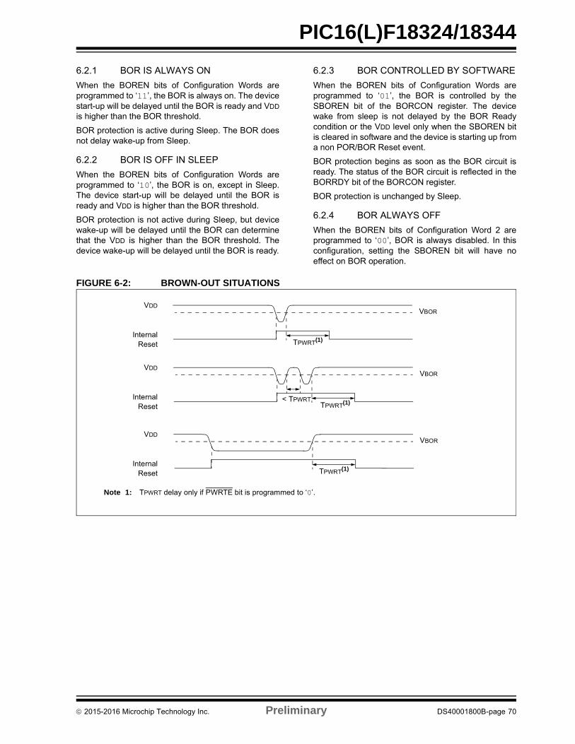
PIC16(L)F18324/18344
6.2.1 BOR IS ALWAYS ON
When the BOREN bits of Configuration Words areprogrammed to ‘11’, the BOR is always on. The devicestart-up will be delayed until the BOR is ready and VDD
is higher than the BOR threshold.
BOR protection is active during Sleep. The BOR doesnot delay wake-up from Sleep.
6.2.2 BOR IS OFF IN SLEEP
When the BOREN bits of Configuration Words areprogrammed to ‘10’, the BOR is on, except in Sleep.The device start-up will be delayed until the BOR isready and VDD is higher than the BOR threshold.
BOR protection is not active during Sleep, but devicewake-up will be delayed until the BOR can determinethat the VDD is higher than the BOR threshold. Thedevice wake-up will be delayed until the BOR is ready.
6.2.3 BOR CONTROLLED BY SOFTWARE
When the BOREN bits of Configuration Words areprogrammed to ‘01’, the BOR is controlled by theSBOREN bit of the BORCON register. The devicewake from sleep is not delayed by the BOR Readycondition or the VDD level only when the SBOREN bitis cleared in software and the device is starting up froma non POR/BOR Reset event.
BOR protection begins as soon as the BOR circuit isready. The status of the BOR circuit is reflected in theBORRDY bit of the BORCON register.
BOR protection is unchanged by Sleep.
6.2.4 BOR ALWAYS OFF
When the BOREN bits of Configuration Word 2 areprogrammed to ‘00’, BOR is always disabled. In thisconfiguration, setting the SBOREN bit will have noeffect on BOR operation.
FIGURE 6-2: BROWN-OUT SITUATIONS
TPWRT(1)
VBOR VDD
InternalReset
VBOR VDD
InternalReset TPWRT(1)< TPWRT
TPWRT(1)
VBOR VDD
InternalReset
Note 1: TPWRT delay only if PWRTE bit is programmed to ‘0’.
2015-2016 Microchip Technology Inc. Preliminary DS40001800B-page 70
PIC16(L)F18324/18344
6.3 Low-Power Brown-out Reset (LPBOR)
The Low-Power Brown-Out Reset (LPBOR) circuitprovides alternative protection against Brown-outconditions. When VDD falls below the LPBORthreshold, the device is held in Reset. When thisoccurs, the BOR bit of the PCON0 register is cleared toindicate that a Brown-out Reset occurred. The BOR bitwill be cleared when either the BOR or the LPBORcircuitry detects a BOR condition. The LPBOR featurecan be used with or without BOR enabled.
When used while BOR is enabled, the LPBOR can beused as a secondary protection circuit in case the BORcircuit fails to detect the BOR condition. Additionally,when BOR is enabled except while in Sleep(BOREN<1:0> = 10), the LPBOR circuit will hold thedevice in Reset while VDD is lower than the LPBORthreshold, and will also re-arm the POR. (seeTable 35-11 for LPBOR Reset voltage levels).
When used without BOR enabled, the LPBOR circuitprovides a single Reset trip point with the benefit ofreduced current consumption.
6.3.1 ENABLING LPBOR
The LPBOR is controlled by the LPBOR bit ofConfiguration Words. When the device is erased, theLPBOR module defaults to disabled.
6.3.1.1 LPBOR Module Output
The output of the LPBOR module is a signal indicatingwhether or not a Reset is to be asserted. This signal isOR’d together with the Reset signal of the BORmodule to provide the generic BOR signal, which goesto the PCON0 register and to the power control block.
6.4 MCLR
The MCLR is an optional external input that can resetthe device. The MCLR function is controlled by theMCLRE bit of Configuration Words and the LVP bit ofConfiguration Words (Table 6-2).
6.4.1 MCLR ENABLED
When MCLR is enabled and the pin is held low, thedevice is held in Reset. The MCLR pin is connected toVDD through an internal weak pull-up.
The device has a noise filter in the MCLR Reset path.The filter will detect and ignore small pulses.
6.4.2 MCLR DISABLED
When MCLR is disabled, the pin functions as a generalpurpose input and the internal weak pull-up is undersoftware control. See Section 12.2 “PORTARegisters” for more information.
6.5 Watchdog Timer (WDT) Reset
The Watchdog Timer generates a Reset if the firmwaredoes not issue a CLRWDT instruction within the time-outperiod. The TO and PD bits in the STATUS register arechanged to indicate the WDT Reset. See Section 10.0“Watchdog Timer (WDT)” for more information.
6.6 RESET Instruction
A RESET instruction will cause a device Reset. The RIbit in the PCON0 register will be set to ‘0’. See Table 6-4for default conditions after a RESET instruction hasoccurred.
6.7 Stack Overflow/Underflow Reset
The device can reset when the Stack overflows orunderflows. The STKOVF or STKUNF bits of the PCON0register indicate the Reset condition. These Resets areenabled by setting the STVREN bit in ConfigurationWords. See Section 4.4 “Stack” for more information.
6.8 Programming Mode Exit
Upon exit of programming mode, the device willbehave as if a device Reset had just occurred.
6.9 Power-up Timer
The Power-up Timer provides a nominal 64 mstime-out on POR or Brown-out Reset.
The device is held in Reset as long as PWRT is active.The PWRT delay allows additional time for the VDD torise to an acceptable level. The Power-up Timer isenabled by clearing the PWRTE bit in ConfigurationWords.
The Power-up Timer starts after the release of the PORand BOR.
For additional information, refer to Application NoteAN607, “Power-up Trouble Shooting” (DS00607).
TABLE 6-2: MCLR CONFIGURATION
MCLRE LVP MCLR
0 0 Disabled
1 0 Enabled
x 1 Enabled
Note: A Reset does not drive the MCLR pin low.
2015-2016 Microchip Technology Inc. Preliminary DS40001800B-page 71
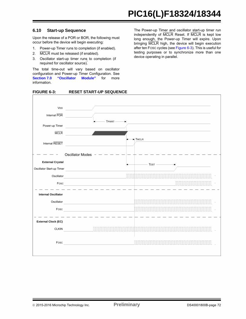
PIC16(L)F18324/18344
6.10 Start-up Sequence
Upon the release of a POR or BOR, the following mustoccur before the device will begin executing:
1. Power-up Timer runs to completion (if enabled).
2. MCLR must be released (if enabled).
3. Oscillator start-up timer runs to completion (ifrequired for oscillator source).
The total time-out will vary based on oscillatorconfiguration and Power-up Timer Configuration. SeeSection 7.0 “Oscillator Module” for moreinformation.
The Power-up Timer and oscillator start-up timer runindependently of MCLR Reset. If MCLR is kept lowlong enough, the Power-up Timer will expire. Uponbringing MCLR high, the device will begin executionafter ten FOSC cycles (see Figure 6-3). This is useful fortesting purposes or to synchronize more than onedevice operating in parallel.
FIGURE 6-3: RESET START-UP SEQUENCE
TOST
TMCLR
TPWRT
VDD
Internal POR
Power-up Timer
MCLR
Internal RESET
Oscillator Modes
Oscillator Start-up Timer
Oscillator
FOSC
Internal Oscillator
Oscillator
FOSC
External Clock (EC)
CLKIN
FOSC
External Crystal
2015-2016 Microchip Technology Inc. Preliminary DS40001800B-page 72
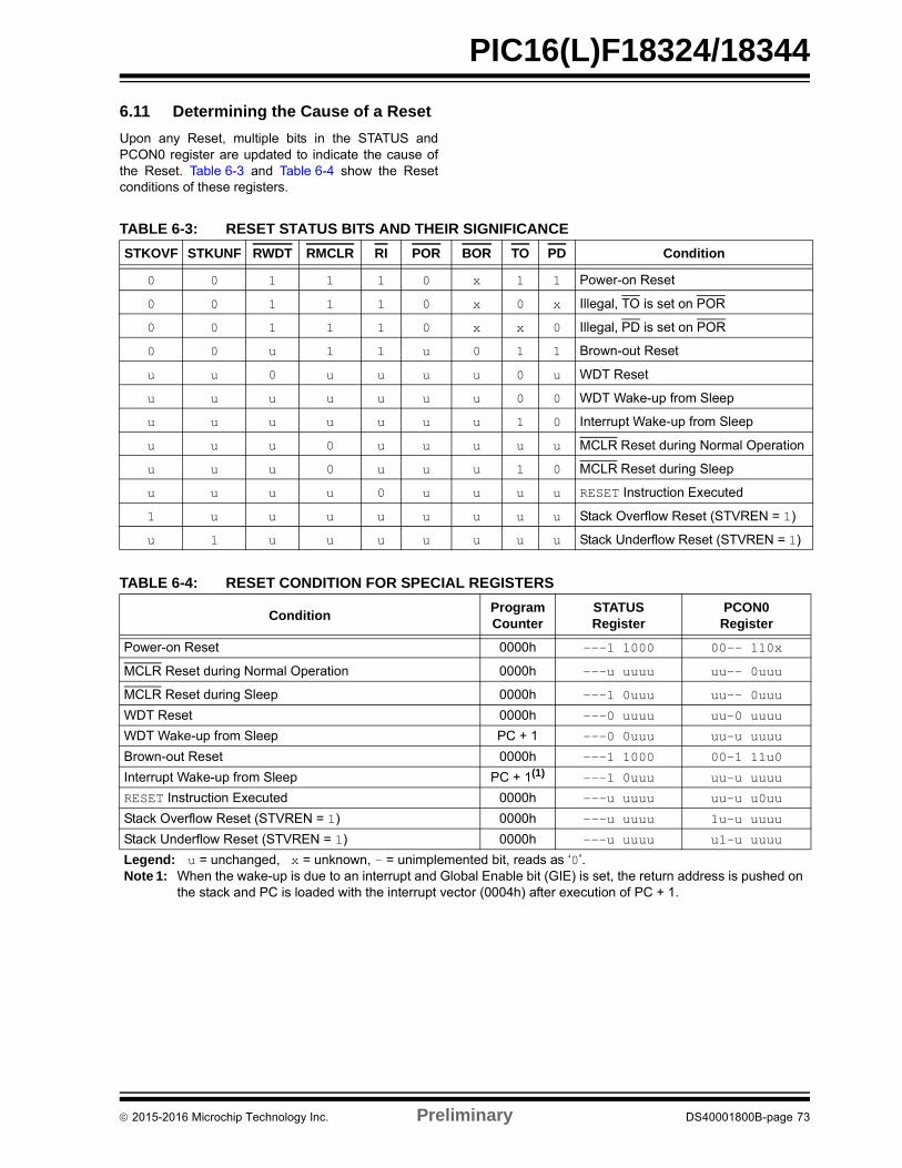
PIC16(L)F18324/18344
6.11 Determining the Cause of a Reset
Upon any Reset, multiple bits in the STATUS andPCON0 register are updated to indicate the cause ofthe Reset. Table 6-3 and Table 6-4 show the Resetconditions of these registers.
TABLE 6-3: RESET STATUS BITS AND THEIR SIGNIFICANCE
STKOVF STKUNF RWDT RMCLR RI POR BOR TO PD Condition
0 0 1 1 1 0 x 1 1 Power-on Reset
0 0 1 1 1 0 x 0 x Illegal, TO is set on POR
0 0 1 1 1 0 x x 0 Illegal, PD is set on POR
0 0 u 1 1 u 0 1 1 Brown-out Reset
u u 0 u u u u 0 u WDT Reset
u u u u u u u 0 0 WDT Wake-up from Sleep
u u u u u u u 1 0 Interrupt Wake-up from Sleep
u u u 0 u u u u u MCLR Reset during Normal Operation
u u u 0 u u u 1 0 MCLR Reset during Sleep
u u u u 0 u u u u RESET Instruction Executed
1 u u u u u u u u Stack Overflow Reset (STVREN = 1)
u 1 u u u u u u u Stack Underflow Reset (STVREN = 1)
TABLE 6-4: RESET CONDITION FOR SPECIAL REGISTERS
ConditionProgramCounter
STATUSRegister
PCON0Register
Power-on Reset 0000h ---1 1000 00-- 110x
MCLR Reset during Normal Operation 0000h ---u uuuu uu-- 0uuu
MCLR Reset during Sleep 0000h ---1 0uuu uu-- 0uuu
WDT Reset 0000h ---0 uuuu uu-0 uuuu
WDT Wake-up from Sleep PC + 1 ---0 0uuu uu-u uuuu
Brown-out Reset 0000h ---1 1000 00-1 11u0
Interrupt Wake-up from Sleep PC + 1(1) ---1 0uuu uu-u uuuu
RESET Instruction Executed 0000h ---u uuuu uu-u u0uu
Stack Overflow Reset (STVREN = 1) 0000h ---u uuuu 1u-u uuuu
Stack Underflow Reset (STVREN = 1) 0000h ---u uuuu u1-u uuuu
Legend: u = unchanged, x = unknown, - = unimplemented bit, reads as ‘0’.Note 1: When the wake-up is due to an interrupt and Global Enable bit (GIE) is set, the return address is pushed on
the stack and PC is loaded with the interrupt vector (0004h) after execution of PC + 1.
2015-2016 Microchip Technology Inc. Preliminary DS40001800B-page 73
PIC16(L)F18324/18344
6.12 Register Definitions: Brown-out Reset Control
REGISTER 6-1: BORCON: BROWN-OUT RESET CONTROL REGISTER
R/W-1/u R/W-0/0 U-0 U-0 U-0 U-0 U-0 R-q/u
SBOREN(1) Reserved — — — — — BORRDY
bit 7 bit 0
Legend:
R = Readable bit W = Writable bit U = Unimplemented bit, read as ‘0’
u = Bit is unchanged x = Bit is unknown -n/n = Value at POR and BOR/Value at all other Resets
‘1’ = Bit is set ‘0’ = Bit is cleared q = Value depends on condition
bit 7 SBOREN: Software Brown-out Reset Enable bit(1)
If BOREN <1:0> in Configuration Words 01:SBOREN is read/write, but has no effect on the BOR.If BOREN <1:0> in Configuration Words = 01:1 = BOR Enabled0 = BOR Disabled
bit 6 Reserved: Bit must be maintained as ‘0’.
bit 5-1 Unimplemented: Read as ‘0’
bit 0 BORRDY: Brown-out Reset Circuit Ready Status bit1 = The Brown-out Reset circuit is active0 = The Brown-out Reset circuit is inactive
Note 1: BOREN<1:0> bits are located in Configuration Words.
2015-2016 Microchip Technology Inc. Preliminary DS40001800B-page 74
PIC16(L)F18324/18344
6.13 Power Control (PCON) Register
The Power Control (PCON) register contains flag bitsto differentiate between a:
• Power-on Reset (POR)
• Brown-out Reset (BOR)
• Reset Instruction Reset (RI)
• MCLR Reset (RMCLR)
• Watchdog Timer Reset (RWDT)
• Stack Underflow Reset (STKUNF)
• Stack Overflow Reset (STKOVF)
The PCON0 register bits are shown in Register 6-2.
Hardware will change the corresponding register bitduring the reset process; if the Reset was not causedby the condition, the bit remains unchanged(Table 6-4).
Software should reset the bit to the inactive state afterthe restart (hardware will not reset the bit).
Software may also set any PCON bit to the active state,so that user code may be tested, but no reset action willbe generated.
6.14 Register Definitions: Power Control
REGISTER 6-2: PCON0: POWER CONTROL REGISTER 0
R/W/HS-0/q R/W/HS-0/q U-0 R/W/HC-1/q R/W/HC-1/q R/W/HC-1/q R/W/HC-q/u R/W/HC-q/u
STKOVF STKUNF — RWDT RMCLR RI POR BOR
bit 7 bit 0
Legend:
HC = Bit is cleared by hardware HS = Bit is set by hardware
R = Readable bit W = Writable bit U = Unimplemented bit, read as ‘0’
u = Bit is unchanged x = Bit is unknown -m/n = Value at POR and BOR/Value at all other Resets
‘1’ = Bit is set ‘0’ = Bit is cleared q = Value depends on condition
bit 7 STKOVF: Stack Overflow Flag bit1 = A Stack Overflow occurred0 = A Stack Overflow has not occurred or has been cleared by firmware
bit 6 STKUNF: Stack Underflow Flag bit1 = A Stack Underflow occurred0 = A Stack Underflow has not occurred or has been cleared by firmware
bit 5 Unimplemented: Read as ‘0’
bit 4 RWDT: Watchdog Timer Reset Flag bit1 = A Watchdog Timer Reset has not occurred or set to ‘1’ by firmware0 = A Watchdog Timer Reset has occurred (cleared by hardware)
bit 3 RMCLR: MCLR Reset Flag bit1 = A MCLR Reset has not occurred or set to ‘1’ by firmware0 = A MCLR Reset has occurred (cleared by hardware)
bit 2 RI: RESET Instruction Flag bit1 = A RESET instruction has not been executed or set to ‘1’ by firmware0 = A RESET instruction has been executed (cleared by hardware)
bit 1 POR: Power-on Reset Status bit1 = No Power-on Reset occurred0 = A Power-on Reset occurred (must be set in software after a Power-on Reset occurs)
bit 0 BOR: Brown-out Reset Status bit1 = No Brown-out Reset occurred0 = A Brown-out Reset occurred (must be set in software after a Power-on Reset or Brown-out Reset
occurs)
2015-2016 Microchip Technology Inc. Preliminary DS40001800B-page 75
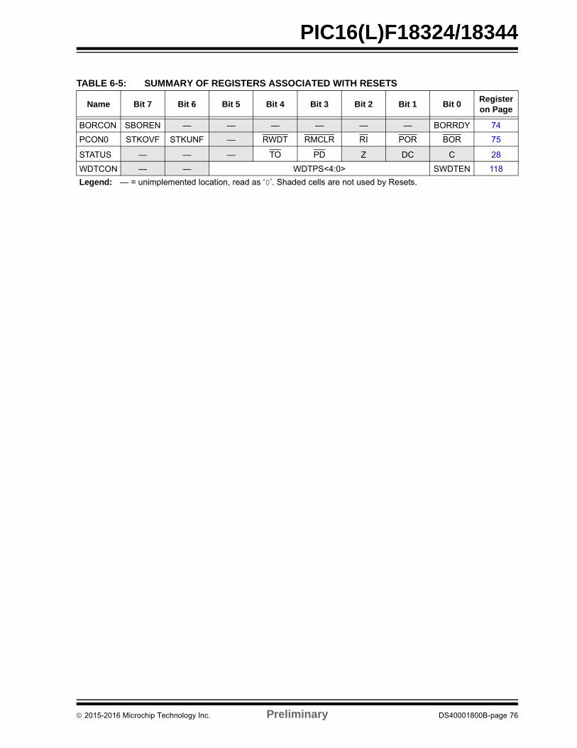
PIC16(L)F18324/18344
TABLE 6-5: SUMMARY OF REGISTERS ASSOCIATED WITH RESETS
Name Bit 7 Bit 6 Bit 5 Bit 4 Bit 3 Bit 2 Bit 1 Bit 0Register on Page
BORCON SBOREN — — — — — — BORRDY 74
PCON0 STKOVF STKUNF — RWDT RMCLR RI POR BOR 75
STATUS — — — TO PD Z DC C 28
WDTCON — — WDTPS<4:0> SWDTEN 118
Legend: — = unimplemented location, read as ‘0’. Shaded cells are not used by Resets.
2015-2016 Microchip Technology Inc. Preliminary DS40001800B-page 76
PIC16(L)F18324/18344
7.0 OSCILLATOR MODULE
7.1 Overview
The oscillator module has a wide variety of clocksources and selection features that allow it to be usedin a wide range of applications while maximizingperformance and minimizing power consumption.Figure 7-1 illustrates a block diagram of the oscillatormodule.
Clock sources can be supplied from external oscillators,quartz-crystal resonators and ceramic resonators. Inaddition, the system clock source can be supplied fromone of two internal oscillators and PLL circuits, with achoice of speeds selectable via software. Additionalclock features include:
• Selectable system clock source between external or internal sources via software.
• Fail-Safe Clock Monitor (FSCM) designed to detect a failure of the external clock source (LP, XT, HS, ECH, ECM, ECL) and switch automati-cally to the internal oscillator.
• Oscillator Start-up Timer (OST) ensures stability of crystal oscillator sources.
The RSTOSC bits of Configuration Word 1 determinethe type of oscillator that will be used when the deviceis reset, including when it is first powered up.
The internal clock modes, LFINTOSC, HFINTOSC (setat 1 MHz), or HFINTOSC (set at 32 MHz) can be setthrough the RSTOSC bits.
If an external clock source is selected, the FEXTOSCbits of Configuration Word 1 must be used inconjunction with the RSTOSC bits to select theExternal Clock mode.
The external oscillator module can be configured in oneof the following clock modes by setting theFEXTOSC<2:0> bits of Configuration Word 1:
1. ECL – External Clock Low-Power mode(<= 100 MHz)
2. ECM – External Clock Medium-Power mode(<= 8 MHz)
3. ECH – External Clock High-Power mode(<= 32 MHz)
4. LP – 32 kHz Low-Power Crystal mode.
5. XT – Medium Gain Crystal or Ceramic ResonatorOscillator mode (between 100 MHz and 4 MHz)
6. HS – High Gain Crystal or Ceramic Resonatormode (above 4 MHz)
The ECH, ECM, and ECL clock modes rely on anexternal logic level signal as the device clock source.The LP, XT, and HS clock modes require an externalcrystal or resonator to be connected to the device.Each mode is optimized for a different frequency range.The INTOSC internal oscillator block produces low andhigh-frequency clock sources, designated LFINTOSCand HFINTOSC. (see Internal Oscillator Block,Figure 7-1).
2015-2016 Microchip Technology Inc. Preliminary DS40001800B-page 77
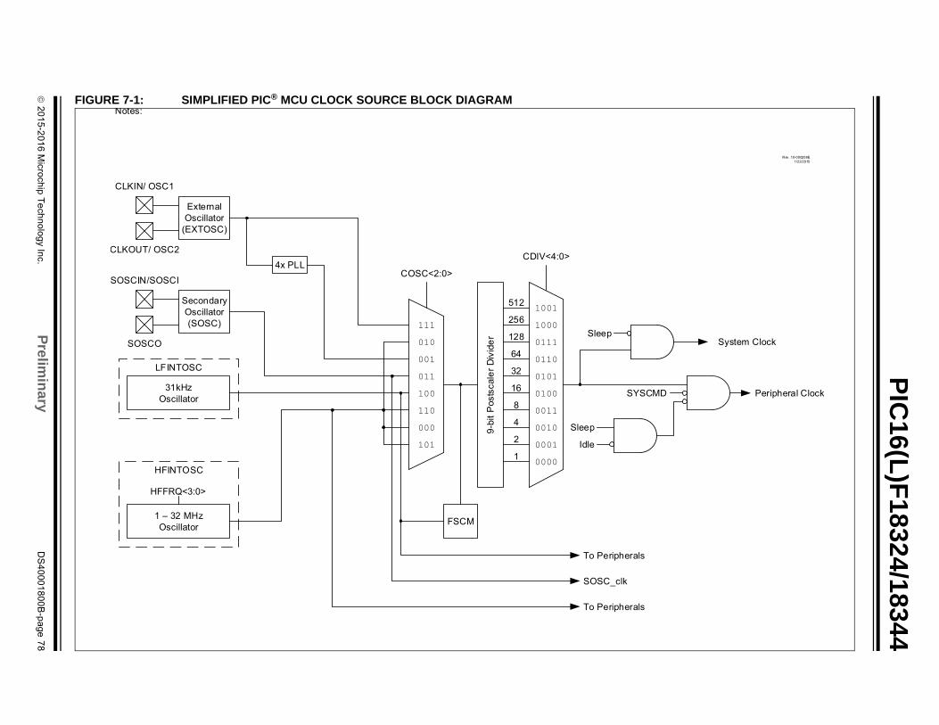
2
01
5-2
01
6 M
icroch
ip T
ech
no
log
y Inc.
Prelim
inary
DS
40
00
18
00
B-p
ag
e 7
8
PIC
16(L)F
18324/18344
FIG
Rev. 10-000208E1/22/2015
System Clock
Peripheral Clock
URE 7-1: SIMPLIFIED PIC® MCU CLOCK SOURCE BLOCK DIAGRAMNotes:
HFFRQ< :0>
HFINTOSC
SecondaryOscillator(SOSC)
ExternalOscillator
(EXTOSC)
CLKIN/ OSC1
CLKOUT/ OSC2
SOSCIN/SOSCI
SOSCO
31kHzOscillator
4x PLL
101
100110000
011001010111
COSC<2:0>
LFINTOSC
1 – 32 MHzOscillator
9-bi
t Pos
tsca
ler D
ivid
er
10001001
0000
001100100001
0100010101100111
512
256
128
64
32
16
8
4
2
1
CDIV<4:0>
Sleep
Idle
Sleep
SYSCMD
FSCM
SOSC_clk
To Peripherals
To Peripherals
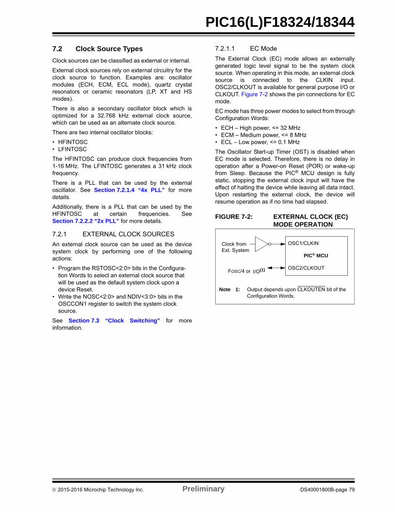
PIC16(L)F18324/18344
7.2 Clock Source Types
Clock sources can be classified as external or internal.
External clock sources rely on external circuitry for theclock source to function. Examples are: oscillatormodules (ECH, ECM, ECL mode), quartz crystalresonators or ceramic resonators (LP, XT and HSmodes).
There is also a secondary oscillator block which isoptimized for a 32.768 kHz external clock source,which can be used as an alternate clock source.
There are two internal oscillator blocks:
• HFINTOSC• LFINTOSC
The HFINTOSC can produce clock frequencies from1-16 MHz. The LFINTOSC generates a 31 kHz clockfrequency.
There is a PLL that can be used by the externaloscillator. See Section 7.2.1.4 “4x PLL” for moredetails.
Additionally, there is a PLL that can be used by theHFINTOSC at certain frequencies. SeeSection 7.2.2.2 “2x PLL” for more details.
7.2.1 EXTERNAL CLOCK SOURCES
An external clock source can be used as the devicesystem clock by performing one of the followingactions:
• Program the RSTOSC<2:0> bits in the Configura-tion Words to select an external clock source that will be used as the default system clock upon a device Reset.
• Write the NOSC<2:0> and NDIV<3:0> bits in the OSCCON1 register to switch the system clock source.
See Section 7.3 “Clock Switching” for moreinformation.
7.2.1.1 EC Mode
The External Clock (EC) mode allows an externallygenerated logic level signal to be the system clocksource. When operating in this mode, an external clocksource is connected to the CLKIN input.OSC2/CLKOUT is available for general purpose I/O orCLKOUT. Figure 7-2 shows the pin connections for ECmode.
EC mode has three power modes to select from throughConfiguration Words:
• ECH – High power, <= 32 MHz• ECM – Medium power, <= 8 MHz• ECL – Low power, <= 0.1 MHz
The Oscillator Start-up Timer (OST) is disabled whenEC mode is selected. Therefore, there is no delay inoperation after a Power-on Reset (POR) or wake-upfrom Sleep. Because the PIC® MCU design is fullystatic, stopping the external clock input will have theeffect of halting the device while leaving all data intact.Upon restarting the external clock, the device willresume operation as if no time had elapsed.
FIGURE 7-2: EXTERNAL CLOCK (EC) MODE OPERATION
OSC1/CLKIN
OSC2/CLKOUT
Clock fromExt. System
PIC® MCU
FOSC/4 or I/O(1)
Note 1: Output depends upon CLKOUTEN bit of the Configuration Words.
2015-2016 Microchip Technology Inc. Preliminary DS40001800B-page 79
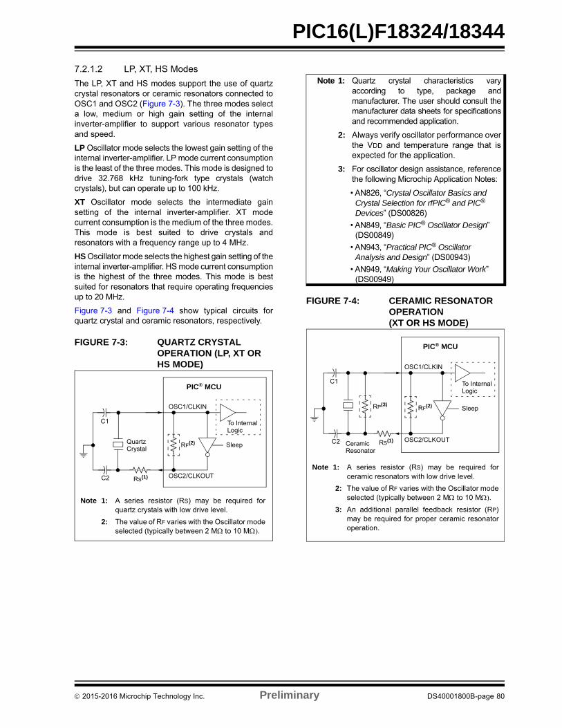
PIC16(L)F18324/18344
7.2.1.2 LP, XT, HS Modes
The LP, XT and HS modes support the use of quartzcrystal resonators or ceramic resonators connected toOSC1 and OSC2 (Figure 7-3). The three modes selecta low, medium or high gain setting of the internalinverter-amplifier to support various resonator typesand speed.
LP Oscillator mode selects the lowest gain setting of theinternal inverter-amplifier. LP mode current consumptionis the least of the three modes. This mode is designed todrive 32.768 kHz tuning-fork type crystals (watchcrystals), but can operate up to 100 kHz.
XT Oscillator mode selects the intermediate gainsetting of the internal inverter-amplifier. XT modecurrent consumption is the medium of the three modes.This mode is best suited to drive crystals andresonators with a frequency range up to 4 MHz.
HS Oscillator mode selects the highest gain setting of theinternal inverter-amplifier. HS mode current consumptionis the highest of the three modes. This mode is bestsuited for resonators that require operating frequenciesup to 20 MHz.
Figure 7-3 and Figure 7-4 show typical circuits forquartz crystal and ceramic resonators, respectively.
FIGURE 7-3: QUARTZ CRYSTAL OPERATION (LP, XT OR HS MODE)
FIGURE 7-4: CERAMIC RESONATOR OPERATION(XT OR HS MODE)
Note 1: A series resistor (RS) may be required forquartz crystals with low drive level.
2: The value of RF varies with the Oscillator modeselected (typically between 2 M to 10 M.
C1
C2
Quartz
RS(1)
OSC1/CLKIN
RF(2) Sleep
To Internal Logic
PIC® MCU
Crystal
OSC2/CLKOUT
Note 1: Quartz crystal characteristics varyaccording to type, package andmanufacturer. The user should consult themanufacturer data sheets for specificationsand recommended application.
2: Always verify oscillator performance overthe VDD and temperature range that isexpected for the application.
3: For oscillator design assistance, referencethe following Microchip Application Notes:
• AN826, “Crystal Oscillator Basics and Crystal Selection for rfPIC® and PIC® Devices” (DS00826)
• AN849, “Basic PIC® Oscillator Design” (DS00849)
• AN943, “Practical PIC® Oscillator Analysis and Design” (DS00943)
• AN949, “Making Your Oscillator Work” (DS00949)
Note 1: A series resistor (RS) may be required forceramic resonators with low drive level.
2: The value of RF varies with the Oscillator modeselected (typically between 2 M to 10 M.
3: An additional parallel feedback resistor (RP)may be required for proper ceramic resonatoroperation.
C1
C2 Ceramic RS(1)
OSC1/CLKIN
RF(2) Sleep
To Internal Logic
PIC® MCU
RP(3)
Resonator
OSC2/CLKOUT
2015-2016 Microchip Technology Inc. Preliminary DS40001800B-page 80
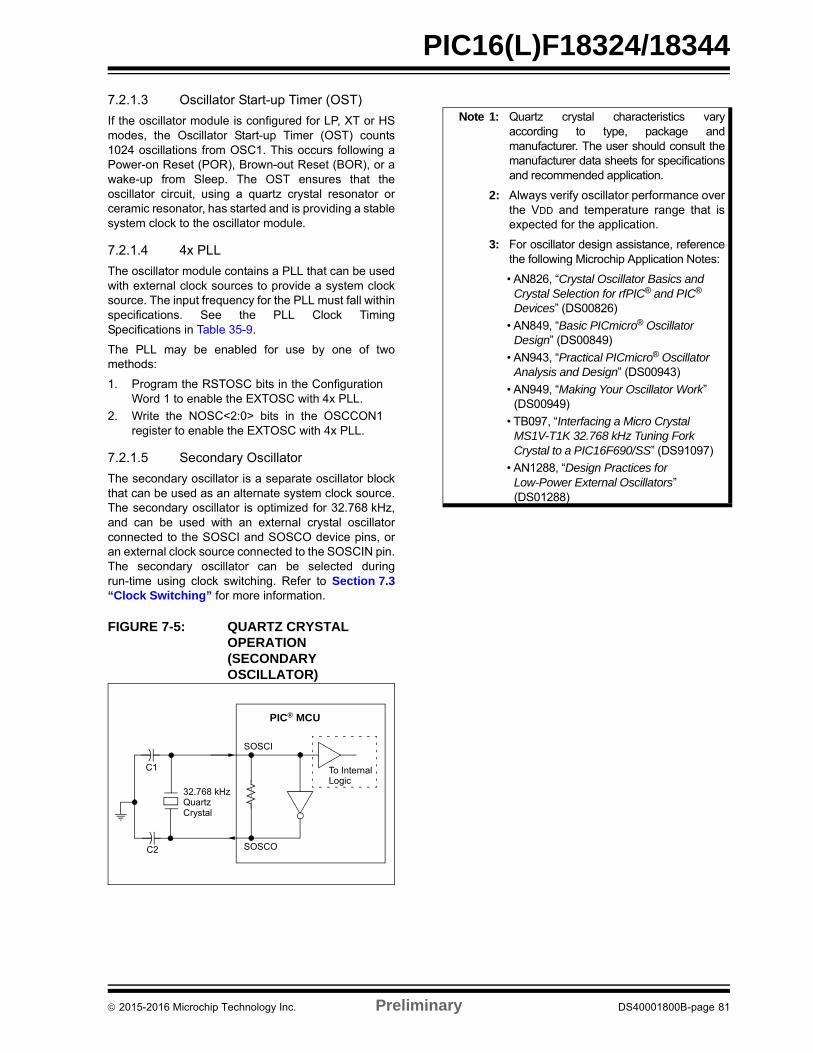
PIC16(L)F18324/18344
7.2.1.3 Oscillator Start-up Timer (OST)
If the oscillator module is configured for LP, XT or HSmodes, the Oscillator Start-up Timer (OST) counts1024 oscillations from OSC1. This occurs following aPower-on Reset (POR), Brown-out Reset (BOR), or awake-up from Sleep. The OST ensures that theoscillator circuit, using a quartz crystal resonator orceramic resonator, has started and is providing a stablesystem clock to the oscillator module.
7.2.1.4 4x PLL
The oscillator module contains a PLL that can be usedwith external clock sources to provide a system clocksource. The input frequency for the PLL must fall withinspecifications. See the PLL Clock TimingSpecifications in Table 35-9.
The PLL may be enabled for use by one of twomethods:
1. Program the RSTOSC bits in the ConfigurationWord 1 to enable the EXTOSC with 4x PLL.
2. Write the NOSC<2:0> bits in the OSCCON1register to enable the EXTOSC with 4x PLL.
7.2.1.5 Secondary Oscillator
The secondary oscillator is a separate oscillator blockthat can be used as an alternate system clock source.The secondary oscillator is optimized for 32.768 kHz,and can be used with an external crystal oscillatorconnected to the SOSCI and SOSCO device pins, oran external clock source connected to the SOSCIN pin.The secondary oscillator can be selected duringrun-time using clock switching. Refer to Section 7.3“Clock Switching” for more information.
FIGURE 7-5: QUARTZ CRYSTAL OPERATION (SECONDARY OSCILLATOR)
C1
C2
32.768 kHz
SOSCI
To Internal Logic
PIC® MCU
Crystal
SOSCO
Quartz
Note 1: Quartz crystal characteristics varyaccording to type, package andmanufacturer. The user should consult themanufacturer data sheets for specificationsand recommended application.
2: Always verify oscillator performance overthe VDD and temperature range that isexpected for the application.
3: For oscillator design assistance, referencethe following Microchip Application Notes:
• AN826, “Crystal Oscillator Basics and Crystal Selection for rfPIC® and PIC® Devices” (DS00826)
• AN849, “Basic PICmicro® Oscillator Design” (DS00849)
• AN943, “Practical PICmicro® Oscillator Analysis and Design” (DS00943)
• AN949, “Making Your Oscillator Work” (DS00949)
• TB097, “Interfacing a Micro Crystal MS1V-T1K 32.768 kHz Tuning Fork Crystal to a PIC16F690/SS” (DS91097)
• AN1288, “Design Practices for Low-Power External Oscillators” (DS01288)
2015-2016 Microchip Technology Inc. Preliminary DS40001800B-page 81
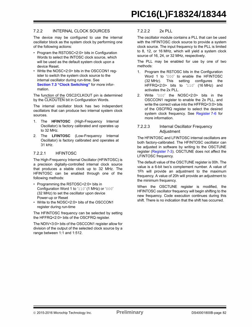
PIC16(L)F18324/18344
7.2.2 INTERNAL CLOCK SOURCES
The device may be configured to use the internaloscillator block as the system clock by performing oneof the following actions:
• Program the RSTOSC<2:0> bits in Configuration Words to select the INTOSC clock source, which will be used as the default system clock upon a device Reset.
• Write the NOSC<2:0> bits in the OSCCON1 reg-ister to switch the system clock source to the internal oscillator during run-time. See Section 7.3 “Clock Switching” for more infor-mation.
The function of the OSC2/CLKOUT pin is determinedby the CLKOUTEN bit in Configuration Words.
The internal oscillator block has two independentoscillators that can produce two internal system clocksources.
1. The HFINTOSC (High-Frequency InternalOscillator) is factory calibrated and operates upto 32 MHz.
2. The LFINTOSC (Low-Frequency InternalOscillator) is factory calibrated and operates at31 kHz.
7.2.2.1 HFINTOSC
The High-Frequency Internal Oscillator (HFINTOSC) isa precision digitally-controlled internal clock sourcethat produces a stable clock up to 32 MHz. TheHFINTOSC can be enabled through one of thefollowing methods:
• Programming the RSTOSC<2:0> bits in Configuration Word 1 to ‘110’ (1 MHz) or ‘000’ (32 MHz) to set the oscillator upon device Power-up or Reset
• Write to the NOSC<2:0> bits of the OSCCON1 register during run-time
The HFINTOSC frequency can be selected by settingthe HFFRQ<2:0> bits of the OSCFRQ register.
The NDIV<3:0> bits of the OSCCON1 register allow fordivision of the output of the selected clock source by arange between 1:1 and 1:512.
7.2.2.2 2x PLL
The oscillator module contains a PLL that can be usedwith the HFINTOSC clock source to provide a systemclock source. The input frequency to the PLL is limitedto 8, 12, or 16 MHz, which will yield a system clocksource of 16, 24, or 32 MHz, respectively.
The PLL may be enabled for use by one of twomethods:
1. Program the RSTOSC bits in the ConfigurationWord 1 to ‘000’ to enable the HFINTOSC(32 MHz). This setting configures theHFFRQ<2:0> bits to ‘110’ (16 MHz) andactivates the 2x PLL.
2. Write ‘000’ the NOSC<2:0> bits in theOSCCON1 register to enable the 2x PLL, andwrite the correct value into the HFFRQ<3:0> bitsof the OSCFRQ register to select the desiredsystem clock frequency. See Register 7-6 formore information.
7.2.2.3 Internal Oscillator Frequency Adjustment
The HFINTOSC and LFINTOSC internal oscillators areboth factory-calibrated. The HFINTOSC oscillator canbe adjusted in software by writing to the OSCTUNEregister (Register 7-3). OSCTUNE does not affect theLFINTOSC frequency.
The default value of the OSCTUNE register is 00h. Thevalue is a 6-bit two’s complement number. A value of1Fh will provide an adjustment to the maximumfrequency. A value of 20h will provide an adjustment tothe minimum frequency.
When the OSCTUNE register is modified, theHFINTOSC oscillator frequency will begin shifting to thenew frequency. Code execution continues during thisshift. There is no indication that the shift has occurred.
2015-2016 Microchip Technology Inc. Preliminary DS40001800B-page 82
PIC16(L)F18324/18344
7.2.2.4 LFINTOSC
The Low-Frequency Internal Oscillator (LFINTOSC) isa factory calibrated 31 kHz internal clock source.
The LFINTOSC is the clock source for the Power-upTimer (PWRT), Watchdog Timer (WDT) and Fail-SafeClock Monitor (FSCM). The LFINTOSC can also beused as the system clock, or as a clock or input sourceto certain peripherals.
The LFINTOSC is selected as the clock source throughone of the following methods:
• Programming the RSTOSC<2:0> bits of Configuration Word 1 to enable LFINTOSC.
• Write to the NOSC<2:0> bits of the OSCCON1 register.
7.2.2.5 Oscillator Status and Manual Enable
The ‘ready’ status of each oscillator is displayed in theOSCSTAT1 register (Register 7-4). The oscillators canalso be manually enabled through the OSCEN register(Register 7-5). Manual enables make it possible toverify the operation of the EXTOSC or SOSC crystaloscillators. This can be achieved by enabling theselected oscillator, then watching the corresponding‘ready’ state of the oscillator in the OSCSTAT1 register.
7.3 Clock Switching
The system clock source can be switched betweenexternal and internal clock sources via software usingthe New Oscillator Source (NOSC) and New DividerSelection Request (NDIV) bits of the OSCCON1register. The following clock sources can be selected:
• External oscillator (EXTOSC)• High-Frequency Internal Oscillator (HFINTOSC)• Low-Frequency Internal Oscillator (LFINTOSC)• Secondary Oscillator (SOSC)• EXTOSC with 4x PLL• HFINTOSC with 2x PLL
7.3.1 NEW OSCILLATOR SOURCE (NOSC) AND NEW DIVIDER SELECTION REQUEST (NDIV) BITS
The New Oscillator Source (NOSC) and New DividerSelection Request (NDIV) bits of the OSCCON1register select the system clock source and frequenciesthat are used for the CPU and peripherals.
When the new values of NOSC<2:0> and NDIV<3:0>are written to OSCCON1, the current oscillatorselection will continue to operate as the system clockwhile waiting for the new source to indicate that it isstable and ready. In some cases, the newly requestedsource may already be in use, and is readyimmediately. In the case of a divider-only change, thenew and old sources are the same and are readyimmediately. The device may enter Sleep while waitingfor the switch as described in Section 7.3.3 “ClockSwitch and Sleep”.
When the new oscillator is ready, the New Oscillator isReady (NOSCR) bit of OSCCON3 and the ClockSwitch Interrupt Flag (CSWIF) bit of PIR3 become set(CSWIF = 1). If Clock Switch Interrupts are enabled(CSWIE = 1), an interrupt will be generated at that time.The Oscillator Ready (ORDY) bit of OSCCON3 canalso be polled to determine when the oscillator is readyin lieu of an interrupt.
If the Clock Switch Hold (CSWHOLD) bit of OSCCON3is clear, the oscillator switch will occur when the NewOscillator Ready bit (NOSCR) is set and the interrupt (ifenabled) will be serviced at the new oscillator setting.If CSWHOLD is set, the oscillator switch is suspended,while execution continues using the current (old) clocksource. When the NOSCR bit is set, software should:• set CSWHOLD = 0 so the switch can complete, or• copy COSC into NOSC<2:0> to abandon the
switch.
If DOZE is in effect, the switch occurs on the next clockcycle, whether or not the CPU is operating during thatcycle.
Changing the clock post-divider without changing theclock source (i.e. changing FOSC from 1 MHz to 2 MHz)is handled in the same manner as a clock sourcechange, as described previously. The clock source willalready be active, so the switch is relatively quick.CSWHOLD must be clear (CSWHOLD = 0) for theswitch to complete.
The current COSC and CDIV are indicated in theOSCCON2 register up to the moment when the switchactually occurs, at which time OSCCON2 is updatedand ORDY is set. NOSCR is cleared by hardware toindicate that the switch is complete.
2015-2016 Microchip Technology Inc. Preliminary DS40001800B-page 83
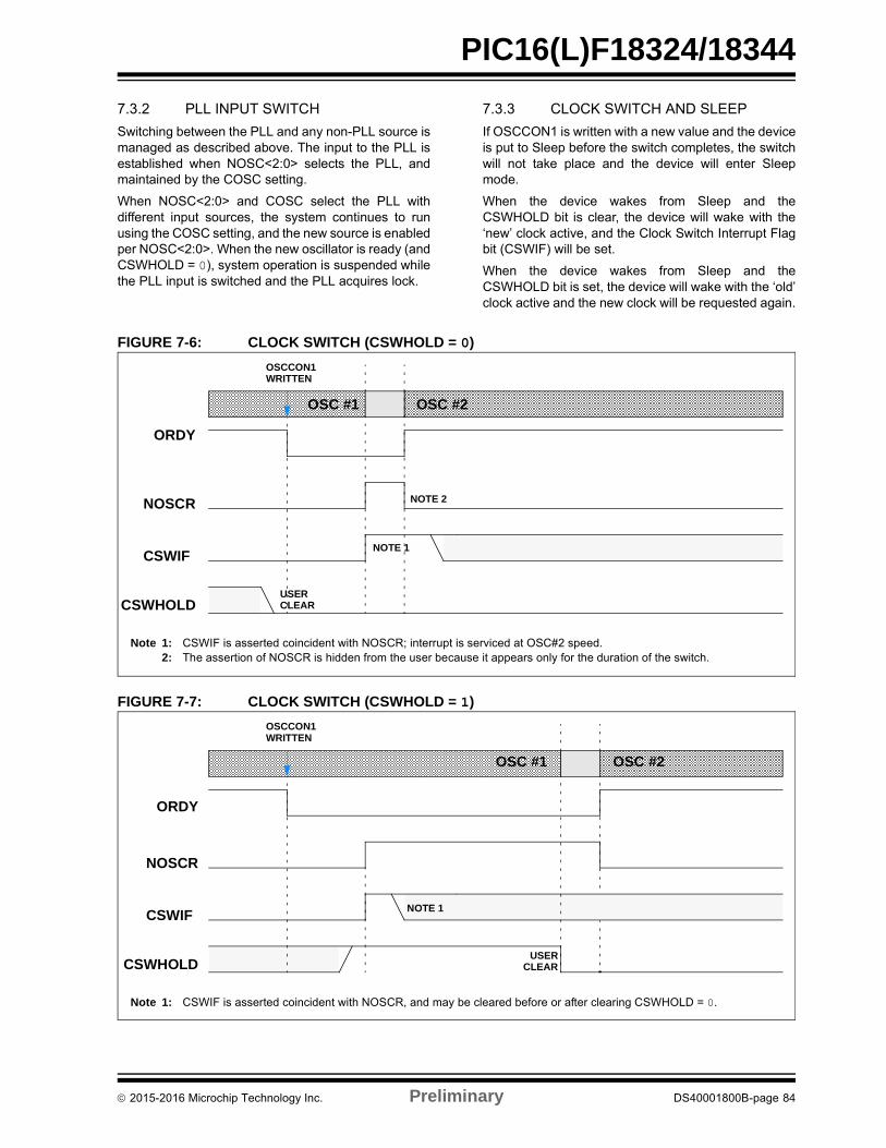
PIC16(L)F18324/18344
7.3.2 PLL INPUT SWITCH
Switching between the PLL and any non-PLL source ismanaged as described above. The input to the PLL isestablished when NOSC<2:0> selects the PLL, andmaintained by the COSC setting.
When NOSC<2:0> and COSC select the PLL withdifferent input sources, the system continues to runusing the COSC setting, and the new source is enabledper NOSC<2:0>. When the new oscillator is ready (andCSWHOLD = 0), system operation is suspended whilethe PLL input is switched and the PLL acquires lock.
7.3.3 CLOCK SWITCH AND SLEEP
If OSCCON1 is written with a new value and the deviceis put to Sleep before the switch completes, the switchwill not take place and the device will enter Sleepmode.
When the device wakes from Sleep and theCSWHOLD bit is clear, the device will wake with the‘new’ clock active, and the Clock Switch Interrupt Flagbit (CSWIF) will be set.
When the device wakes from Sleep and theCSWHOLD bit is set, the device will wake with the ‘old’clock active and the new clock will be requested again.
FIGURE 7-6: CLOCK SWITCH (CSWHOLD = 0)
FIGURE 7-7: CLOCK SWITCH (CSWHOLD = 1)
Note 1: CSWIF is asserted coincident with NOSCR; interrupt is serviced at OSC#2 speed.2: The assertion of NOSCR is hidden from the user because it appears only for the duration of the switch.
CSWHOLD
NOSCR
OSC #2
CSWIF
OSCCON1WRITTEN
NOTE 1
USERCLEAR
OSC #1
NOTE 2
ORDY
Note 1: CSWIF is asserted coincident with NOSCR, and may be cleared before or after clearing CSWHOLD = 0.
CSWHOLD
NOSCR
OSC #1 OSC #2
CSWIF
OSCCON1WRITTEN
NOTE 1
ORDY
USERCLEAR
2015-2016 Microchip Technology Inc. Preliminary DS40001800B-page 84
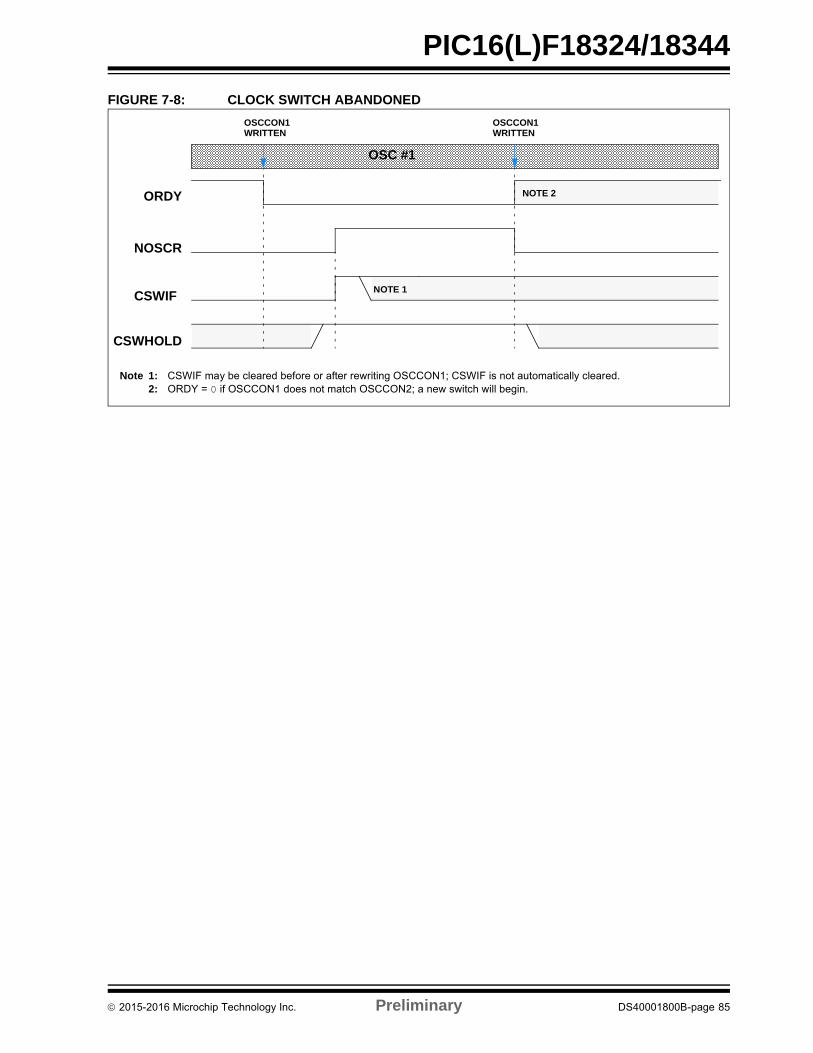
PIC16(L)F18324/18344
FIGURE 7-8: CLOCK SWITCH ABANDONED
Note 1: CSWIF may be cleared before or after rewriting OSCCON1; CSWIF is not automatically cleared.2: ORDY = 0 if OSCCON1 does not match OSCCON2; a new switch will begin.
CSWHOLD
NOSCR
OSC #1
CSWIF
OSCCON1WRITTEN
NOTE 1
OSCCON1WRITTEN
NOTE 2ORDY
2015-2016 Microchip Technology Inc. Preliminary DS40001800B-page 85

PIC16(L)F18324/18344
7.4 Fail-Safe Clock Monitor
The Fail-Safe Clock Monitor (FSCM) allows the deviceto continue operating should the external oscillator fail.The FSCM is enabled by setting the FCMEN bit in theConfiguration Words. The FSCM is applicable to allexternal Oscillator modes (LP, XT, HS, ECL, ECM,ECH, and Secondary Oscillator).
FIGURE 7-9: FSCM BLOCK DIAGRAM
7.4.1 FAIL-SAFE DETECTION
The FSCM module detects a failed oscillator bycomparing the external oscillator to the FSCM sampleclock. The sample clock is generated by dividing theLFINTOSC by 64. See Figure 7-9. Inside the faildetector block is a latch. The external clock sets thelatch on each falling edge of the external clock. Thesample clock clears the latch on each rising edge of thesample clock. A failure is detected when an entirehalf-cycle of the sample clock elapses before theexternal clock goes low.
7.4.2 FAIL-SAFE OPERATION
When the external clock fails, the FSCM switches thedevice clock to the HFINTOSC at 1 MHz clockfrequency and sets the bit flag OSFIF of the PIR3register. Setting this flag will generate an interrupt if theOSFIE bit of the PIE3 register is also set. The devicefirmware can then take steps to mitigate the problemsthat may arise from a failed clock. The system clock willcontinue to be sourced from the internal clock sourceuntil the device firmware successfully restarts theexternal oscillator and switches back to externaloperation, by writing to the NOSC<2:0> andNDIV<3:0>bits of the OSCCON1 register.
7.4.3 FAIL-SAFE CONDITION CLEARING
The Fail-Safe condition is cleared after a Reset,executing a SLEEP instruction or changing theNOSC<2:0> and NDIV<3:0> bits of the OSCCON1register. When switching to the external oscillator orexternal oscillator with PLL, the OST is restarted. Whilethe OST is running, the device continues to operatefrom the INTOSC selected in OSCCON1. When theOST times out, the Fail-Safe condition is cleared aftersuccessfully switching to the external clock source. TheOSFIF bit should be cleared prior to switching to theexternal clock source. If the Fail-Safe condition stillexists, the OSFIF flag will again be set by hardware.
7.4.4 RESET OR WAKE-UP FROM SLEEP
The FSCM is designed to detect an oscillator failureafter the Oscillator Start-up Timer (OST) has expired.The OST is used after waking up from Sleep and afterany type of Reset. The OST is not used with the ECClock modes so that the external clock signal can bestopped if required. Therefore, the device will alwaysbe executing code while the OST is operating whenusing one of the EC modes.
FIGURE 7-10: FSCM TIMING DIAGRAM
External
LFINTOSC÷ 64
S
R
Q
31 kHz(~32 s)
488 Hz(~2 ms)
Clock MonitorLatch
ClockFailure
Detected
Oscillator
Clock
Q
Sample Clock
OSCFIF
SystemClock
Output
Sample Clock
FailureDetected
OscillatorFailure
Note: The system clock is normally at a much higher frequency than the sample clock. The relative frequencies inthis example have been chosen for clarity.
(Q)
Test Test Test
Clock Monitor Output
2015-2016 Microchip Technology Inc. Preliminary DS40001800B-page 86
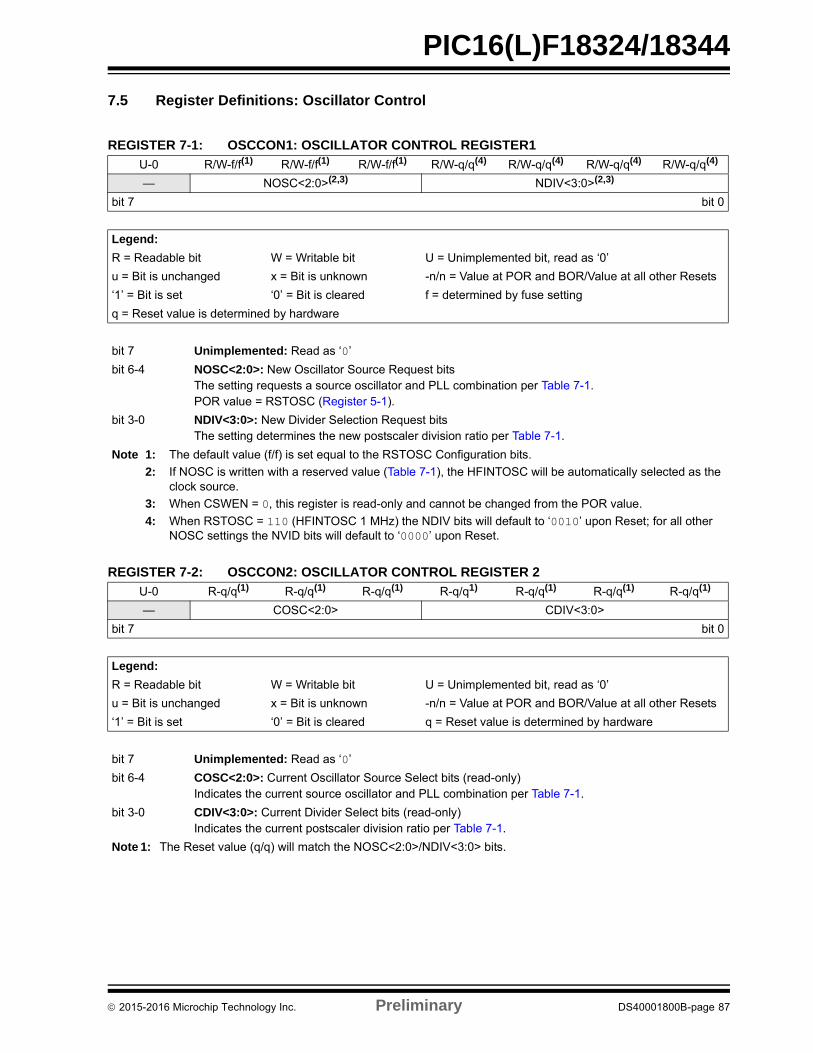
PIC16(L)F18324/18344
7.5 Register Definitions: Oscillator Control
REGISTER 7-1: OSCCON1: OSCILLATOR CONTROL REGISTER1
U-0 R/W-f/f(1) R/W-f/f(1) R/W-f/f(1) R/W-q/q(4) R/W-q/q(4) R/W-q/q(4) R/W-q/q(4)
— NOSC<2:0>(2,3) NDIV<3:0>(2,3)
bit 7 bit 0
Legend:
R = Readable bit W = Writable bit U = Unimplemented bit, read as ‘0’
u = Bit is unchanged x = Bit is unknown -n/n = Value at POR and BOR/Value at all other Resets
‘1’ = Bit is set ‘0’ = Bit is cleared f = determined by fuse setting
q = Reset value is determined by hardware
bit 7 Unimplemented: Read as ‘0’
bit 6-4 NOSC<2:0>: New Oscillator Source Request bitsThe setting requests a source oscillator and PLL combination per Table 7-1.POR value = RSTOSC (Register 5-1).
bit 3-0 NDIV<3:0>: New Divider Selection Request bitsThe setting determines the new postscaler division ratio per Table 7-1.
Note 1: The default value (f/f) is set equal to the RSTOSC Configuration bits.
2: If NOSC is written with a reserved value (Table 7-1), the HFINTOSC will be automatically selected as the clock source.
3: When CSWEN = 0, this register is read-only and cannot be changed from the POR value.
4: When RSTOSC = 110 (HFINTOSC 1 MHz) the NDIV bits will default to ‘0010’ upon Reset; for all other NOSC settings the NVID bits will default to ‘0000’ upon Reset.
REGISTER 7-2: OSCCON2: OSCILLATOR CONTROL REGISTER 2
U-0 R-q/q(1) R-q/q(1) R-q/q(1) R-q/q1) R-q/q(1) R-q/q(1) R-q/q(1)
— COSC<2:0> CDIV<3:0>
bit 7 bit 0
Legend:
R = Readable bit W = Writable bit U = Unimplemented bit, read as ‘0’
u = Bit is unchanged x = Bit is unknown -n/n = Value at POR and BOR/Value at all other Resets
‘1’ = Bit is set ‘0’ = Bit is cleared q = Reset value is determined by hardware
bit 7 Unimplemented: Read as ‘0’
bit 6-4 COSC<2:0>: Current Oscillator Source Select bits (read-only)Indicates the current source oscillator and PLL combination per Table 7-1.
bit 3-0 CDIV<3:0>: Current Divider Select bits (read-only)Indicates the current postscaler division ratio per Table 7-1.
Note 1: The Reset value (q/q) will match the NOSC<2:0>/NDIV<3:0> bits.
2015-2016 Microchip Technology Inc. Preliminary DS40001800B-page 87
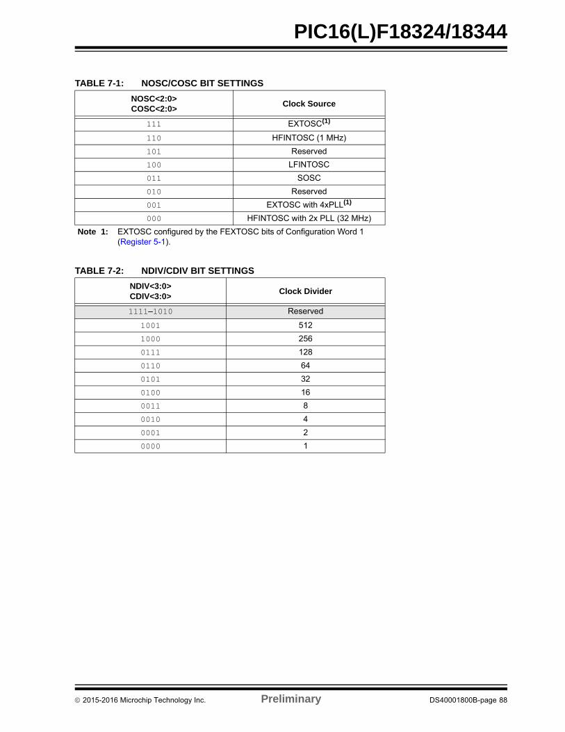
PIC16(L)F18324/18344
TABLE 7-1: NOSC/COSC BIT SETTINGS
NOSC<2:0>COSC<2:0>
Clock Source
111 EXTOSC(1)
110 HFINTOSC (1 MHz)
101 Reserved
100 LFINTOSC
011 SOSC
010 Reserved
001 EXTOSC with 4xPLL(1)
000 HFINTOSC with 2x PLL (32 MHz)
Note 1: EXTOSC configured by the FEXTOSC bits of Configuration Word 1 (Register 5-1).
TABLE 7-2: NDIV/CDIV BIT SETTINGS
NDIV<3:0>CDIV<3:0>
Clock Divider
1111–1010 Reserved
1001 512
1000 256
0111 128
0110 64
0101 32
0100 16
0011 8
0010 4
0001 2
0000 1
2015-2016 Microchip Technology Inc. Preliminary DS40001800B-page 88
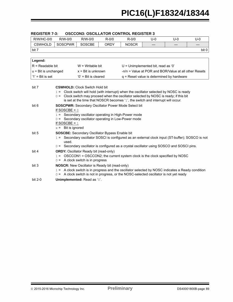
PIC16(L)F18324/18344
REGISTER 7-3: OSCCON3: OSCILLATOR CONTROL REGISTER 3
R/W/HC-0/0 R/W-0/0 R/W-0/0 R-0/0 R-0/0 U-0 U-0 U-0
CSWHOLD SOSCPWR SOSCBE ORDY NOSCR — — —
bit 7 bit 0
Legend:
R = Readable bit W = Writable bit U = Unimplemented bit, read as ‘0’
u = Bit is unchanged x = Bit is unknown -n/n = Value at POR and BOR/Value at all other Resets
‘1’ = Bit is set ‘0’ = Bit is cleared q = Reset value is determined by hardware
bit 7 CSWHOLD: Clock Switch Hold bit1 = Clock switch will hold (with interrupt) when the oscillator selected by NOSC is ready0 = Clock switch may proceed when the oscillator selected by NOSC is ready; if this bit
is set at the time that NOSCR becomes ‘1’, the switch and interrupt will occur.
bit 6 SOSCPWR: Secondary Oscillator Power Mode Select bitIf SOSCBE = 01 = Secondary oscillator operating in High-Power mode0 = Secondary oscillator operating in Low-Power modeIf SOSCBE = 1x = Bit is ignored
bit 5 SOSCBE: Secondary Oscillator Bypass Enable bit1 = Secondary oscillator SOSCI is configured as an external clock input (ST-buffer); SOSCO is not
used.0 = Secondary oscillator is configured as a crystal oscillator using SOSCO and SOSCI pins.
bit 4 ORDY: Oscillator Ready bit (read-only)1 = OSCCON1 = OSCCON2; the current system clock is the clock specified by NOSC0 = A clock switch is in progress
bit 3 NOSCR: New Oscillator is Ready bit (read-only)1 = A clock switch is in progress and the oscillator selected by NOSC indicates a Ready condition0 = A clock switch is not in progress, or the NOSC-selected oscillator is not yet ready
bit 2-0 Unimplemented: Read as ‘0’.
2015-2016 Microchip Technology Inc. Preliminary DS40001800B-page 89
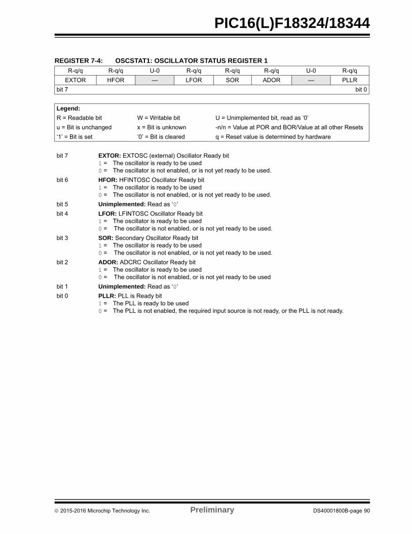
PIC16(L)F18324/18344
REGISTER 7-4: OSCSTAT1: OSCILLATOR STATUS REGISTER 1
R-q/q R-q/q U-0 R-q/q R-q/q R-q/q U-0 R-q/q
EXTOR HFOR — LFOR SOR ADOR — PLLR
bit 7 bit 0
Legend:
R = Readable bit W = Writable bit U = Unimplemented bit, read as ‘0’
u = Bit is unchanged x = Bit is unknown -n/n = Value at POR and BOR/Value at all other Resets
‘1’ = Bit is set ‘0’ = Bit is cleared q = Reset value is determined by hardware
bit 7 EXTOR: EXTOSC (external) Oscillator Ready bit1 = The oscillator is ready to be used0 = The oscillator is not enabled, or is not yet ready to be used.
bit 6 HFOR: HFINTOSC Oscillator Ready bit1 = The oscillator is ready to be used0 = The oscillator is not enabled, or is not yet ready to be used.
bit 5 Unimplemented: Read as ‘0’
bit 4 LFOR: LFINTOSC Oscillator Ready bit1 = The oscillator is ready to be used0 = The oscillator is not enabled, or is not yet ready to be used.
bit 3 SOR: Secondary Oscillator Ready bit1 = The oscillator is ready to be used0 = The oscillator is not enabled, or is not yet ready to be used.
bit 2 ADOR: ADCRC Oscillator Ready bit1 = The oscillator is ready to be used0 = The oscillator is not enabled, or is not yet ready to be used
bit 1 Unimplemented: Read as ‘0’
bit 0 PLLR: PLL is Ready bit1 = The PLL is ready to be used0 = The PLL is not enabled, the required input source is not ready, or the PLL is not ready.
2015-2016 Microchip Technology Inc. Preliminary DS40001800B-page 90
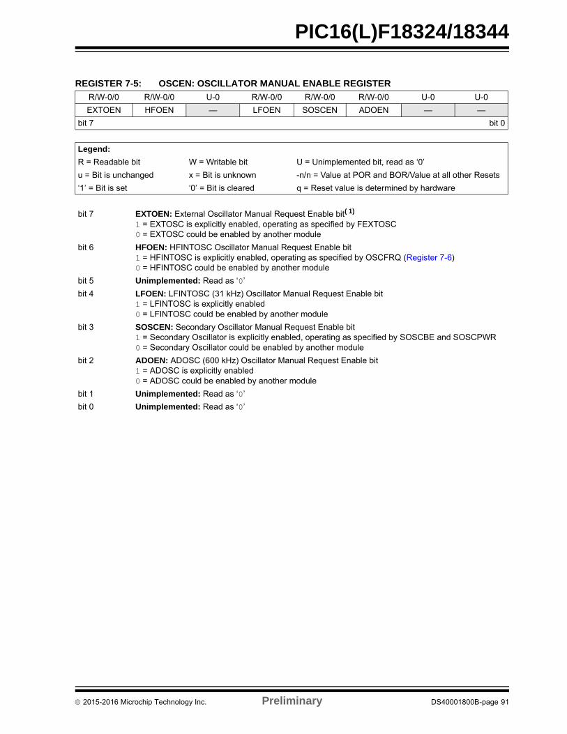
PIC16(L)F18324/18344
REGISTER 7-5: OSCEN: OSCILLATOR MANUAL ENABLE REGISTER
R/W-0/0 R/W-0/0 U-0 R/W-0/0 R/W-0/0 R/W-0/0 U-0 U-0
EXTOEN HFOEN — LFOEN SOSCEN ADOEN — —
bit 7 bit 0
Legend:
R = Readable bit W = Writable bit U = Unimplemented bit, read as ‘0’
u = Bit is unchanged x = Bit is unknown -n/n = Value at POR and BOR/Value at all other Resets
‘1’ = Bit is set ‘0’ = Bit is cleared q = Reset value is determined by hardware
bit 7 EXTOEN: External Oscillator Manual Request Enable bit( 1)
1 = EXTOSC is explicitly enabled, operating as specified by FEXTOSC0 = EXTOSC could be enabled by another module
bit 6 HFOEN: HFINTOSC Oscillator Manual Request Enable bit1 = HFINTOSC is explicitly enabled, operating as specified by OSCFRQ (Register 7-6)0 = HFINTOSC could be enabled by another module
bit 5 Unimplemented: Read as ‘0’
bit 4 LFOEN: LFINTOSC (31 kHz) Oscillator Manual Request Enable bit1 = LFINTOSC is explicitly enabled0 = LFINTOSC could be enabled by another module
bit 3 SOSCEN: Secondary Oscillator Manual Request Enable bit1 = Secondary Oscillator is explicitly enabled, operating as specified by SOSCBE and SOSCPWR0 = Secondary Oscillator could be enabled by another module
bit 2 ADOEN: ADOSC (600 kHz) Oscillator Manual Request Enable bit1 = ADOSC is explicitly enabled0 = ADOSC could be enabled by another module
bit 1 Unimplemented: Read as ‘0’
bit 0 Unimplemented: Read as ‘0’
2015-2016 Microchip Technology Inc. Preliminary DS40001800B-page 91
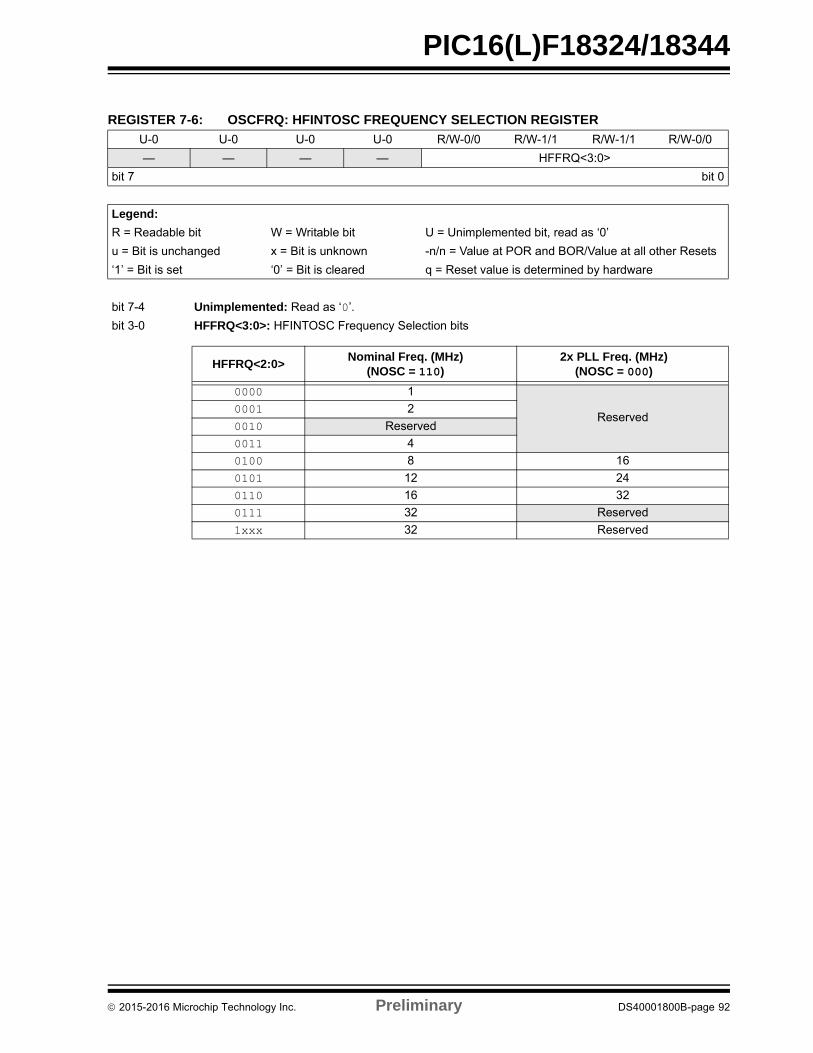
PIC16(L)F18324/18344
REGISTER 7-6: OSCFRQ: HFINTOSC FREQUENCY SELECTION REGISTER
U-0 U-0 U-0 U-0 R/W-0/0 R/W-1/1 R/W-1/1 R/W-0/0
— — — — HFFRQ<3:0>
bit 7 bit 0
Legend:
R = Readable bit W = Writable bit U = Unimplemented bit, read as ‘0’
u = Bit is unchanged x = Bit is unknown -n/n = Value at POR and BOR/Value at all other Resets
‘1’ = Bit is set ‘0’ = Bit is cleared q = Reset value is determined by hardware
bit 7-4 Unimplemented: Read as ‘0’.
bit 3-0 HFFRQ<3:0>: HFINTOSC Frequency Selection bits
HFFRQ<2:0>Nominal Freq. (MHz)
(NOSC = 110)2x PLL Freq. (MHz)
(NOSC = 000)
0000 1
Reserved0001 2
0010 Reserved
0011 4
0100 8 16
0101 12 24
0110 16 32
0111 32 Reserved
1xxx 32 Reserved
2015-2016 Microchip Technology Inc. Preliminary DS40001800B-page 92
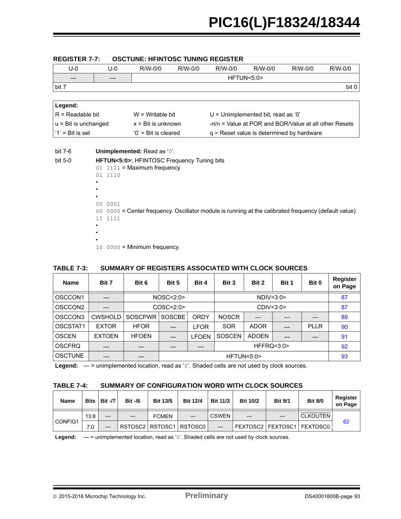
PIC16(L)F18324/18344
REGISTER 7-7: OSCTUNE: HFINTOSC TUNING REGISTER
U-0 U-0 R/W-0/0 R/W-0/0 R/W-0/0 R/W-0/0 R/W-0/0 R/W-0/0
— — HFTUN<5:0>
bit 7 bit 0
Legend:
R = Readable bit W = Writable bit U = Unimplemented bit, read as ‘0’
u = Bit is unchanged x = Bit is unknown -n/n = Value at POR and BOR/Value at all other Resets
‘1’ = Bit is set ‘0’ = Bit is cleared q = Reset value is determined by hardware
bit 7-6 Unimplemented: Read as ‘0’.
bit 5-0 HFTUN<5:0>: HFINTOSC Frequency Tuning bits01 1111 = Maximum frequency01 1110 •••00 0001 00 0000 = Center frequency. Oscillator module is running at the calibrated frequency (default value).11 1111 •••10 0000 = Minimum frequency.
TABLE 7-3: SUMMARY OF REGISTERS ASSOCIATED WITH CLOCK SOURCES
Name Bit 7 Bit 6 Bit 5 Bit 4 Bit 3 Bit 2 Bit 1 Bit 0Register on Page
OSCCON1 — NOSC<2:0> NDIV<3:0> 87
OSCCON2 — COSC<2:0> CDIV<3:0> 87
OSCCON3 CWSHOLD SOSCPWR SOSCBE ORDY NOSCR — — — 89
OSCSTAT1 EXTOR HFOR — LFOR SOR ADOR — PLLR 90
OSCEN EXTOEN HFOEN — LFOEN SOSCEN ADOEN — — 91
OSCFRQ — — — — HFFRQ<3:0> 92
OSCTUNE — — HFTUN<5:0> 93
Legend: — = unimplemented location, read as ‘0’. Shaded cells are not used by clock sources.
TABLE 7-4: SUMMARY OF CONFIGURATION WORD WITH CLOCK SOURCES
Name Bits Bit -/7 Bit -/6 Bit 13/5 Bit 12/4 Bit 11/3 Bit 10/2 Bit 9/1 Bit 8/0Register on Page
CONFIG113:8 — — FCMEN — CSWEN — — CLKOUTEN
627:0 — RSTOSC2 RSTOSC1 RSTOSC0 — FEXTOSC2 FEXTOSC1 FEXTOSC0
Legend: — = unimplemented location, read as ‘0’. Shaded cells are not used by clock sources.
2015-2016 Microchip Technology Inc. Preliminary DS40001800B-page 93
PIC16(L)F18324/18344
8.0 INTERRUPTS
The interrupt feature allows certain events to preemptnormal program flow. Firmware is used to determinethe source of the interrupt and act accordingly. Someinterrupts can be configured to wake the MCU fromSleep mode.
Many peripherals produce interrupts. Refer to thecorresponding chapters for details.
A block diagram of the interrupt logic is shown inFigure 8-1.
FIGURE 8-1: INTERRUPT LOGIC
TMR0IFTMR0IE
INTFINTE
IOCIFIOCIE
Interruptto CPU
Wake-up (If in Sleep mode)
GIE
(TMR1IF) PIR1<0>
PIRn<7>
PEIE
(TMR1IE) PIE1<0>
Peripheral Interrupts
PIEn<7>
2015-2016 Microchip Technology Inc. Preliminary DS40001800B-page 94
PIC16(L)F18324/18344
8.1 Operation
Interrupts are disabled upon any device Reset. Theyare enabled by setting the following bits:
• GIE bit of the INTCON register• Interrupt Enable bit(s) (PIEx bits) for the specific
interrupt event(s)• PEIE bit of the INTCON register
The PIR1, PIR2, PIR3 and PIR4 registers recordindividual interrupts via interrupt flag bits. Interrupt flagbits will be set, regardless of the status of the GIE, PEIEand individual interrupt enable bits.
The following events happen when an interrupt eventoccurs while the GIE bit is set:
• Current prefetched instruction is flushed• GIE bit is cleared• Current Program Counter (PC) is pushed onto the
stack• Critical registers are automatically saved to the
shadow registers (See “Section 8.5 “Automatic Context Saving”)
• PC is loaded with the interrupt vector 0004h
The firmware within the Interrupt Service Routine (ISR)should determine the source of the interrupt by pollingthe interrupt flag bits. The interrupt flag bits must becleared before exiting the ISR to avoid repeatedinterrupts. Because the GIE bit is cleared, any interruptthat occurs while executing the ISR will be recordedthrough its interrupt flag, but will not cause theprocessor to redirect to the interrupt vector.
The RETFIE instruction exits the ISR by popping theprevious address from the stack, restoring the savedcontext from the shadow registers and setting the GIEbit.
For additional information on a specific interrupt’soperation, refer to its peripheral chapter.
8.2 Interrupt Latency
Interrupt latency is defined as the time from when theinterrupt event occurs to the time code execution at theinterrupt vector begins. The interrupt is sampled duringQ1 of the instruction cycle. The actual interrupt latencythen depends on the instruction that is executing at thetime the interrupt is detected. See Figure 8-2 andFigure 8-3 for more details.
Note 1: Individual interrupt flag bits are set,regardless of the state of any otherenable bits.
2: All interrupts will be ignored while the GIEbit is cleared. Any interrupt occurringwhile the GIE bit is clear will be servicedwhen the GIE bit is set again.
2015-2016 Microchip Technology Inc. Preliminary DS40001800B-page 95
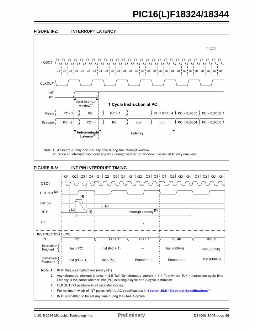
PIC16(L)F18324/18344
FIGURE 8-2: INTERRUPT LATENCY
FIGURE 8-3: INT PIN INTERRUPT TIMING
Rev. 10-000269E8/31/2016
Q1 Q1 Q1 Q1 Q1 Q1 Q1 Q2Q2Q2Q2Q2Q2 Q2Q3 Q3 Q3 Q3 Q3 Q3 Q3 Q4Q4Q4Q4Q4Q4Q4
OSC1
CLKOUT
INT pin
PC - 1 PCFetch
Execute PC - 2 PC - 1 PC
PC + 1 PC = 0x0004
PC = 0x0004
PC = 0x0005
PC = 0x0005
PC = 0x0006
1 Cycle Instruction at PC
Latency
Valid Interrupt window(1)
Indeterminate Latency(2)
Note 1: An interrupt may occur at any time during the interrupt window. 2: Since an interrupt may occur any time during the interrupt window, the actual latency can vary.
Q2Q1 Q3 Q4 Q2Q1 Q3 Q4 Q2Q1 Q3 Q4 Q2Q1 Q3 Q4 Q2Q1 Q3 Q4
OSC1
CLKOUT
INT pin
INTF
GIE
INSTRUCTION FLOW
PC
InstructionFetched
InstructionExecuted
Interrupt Latency
PC PC + 1 PC + 1 0004h 0005h
Inst (0004h) Inst (0005h)
Forced NOP
Inst (PC) Inst (PC + 1)
Inst (PC – 1) Inst (0004h) Forced NOPInst (PC)
—
Note 1: INTF flag is sampled here (every Q1).
2: Asynchronous interrupt latency = 3-5 TCY. Synchronous latency = 3-4 TCY, where TCY = instruction cycle time.Latency is the same whether Inst (PC) is a single cycle or a 2-cycle instruction.
3: CLKOUT not available in all oscillator modes.
4: For minimum width of INT pulse, refer to AC specifications in Section 35.0 “Electrical Specifications””.
5: INTF is enabled to be set any time during the Q4-Q1 cycles.
(1)
(2)
(3)
(4)
(5)(1)
2015-2016 Microchip Technology Inc. Preliminary DS40001800B-page 96
PIC16(L)F18324/18344
8.3 Interrupts During Sleep
All interrupts can be used to wake from Sleep. To wakefrom Sleep, the peripheral must be able to operatewithout the system clock. The interrupt source musthave the appropriate Interrupt Enable bit(s) set prior toentering Sleep.
On waking from Sleep, if the GIE bit is also set, theprocessor will branch to the interrupt vector. Otherwise,the processor will continue executing instructions afterthe SLEEP instruction. The instruction directly after theSLEEP instruction will always be executed beforebranching to the ISR. Refer to Section 9.0“Power-Saving Operation Modes” for more details.
8.4 INT Pin
The INT pin can be used to generate an asynchronousedge-triggered interrupt. This interrupt is enabled bysetting the INTE bit of the PIE0 register. The INTEDG bitof the INTCON register determines on which edge theinterrupt will occur. When the INTEDG bit is set, therising edge will cause the interrupt. When the INTEDGbit is clear, the falling edge will cause the interrupt. TheINTF bit of the PIR0 register will be set when a validedge appears on the INT pin. If the GIE and INTE bitsare also set, the processor will redirect programexecution to the interrupt vector.
8.5 Automatic Context Saving
Upon entering an interrupt, the return PC address issaved on the stack. Additionally, the following registersare automatically saved in the shadow registers:
• W register
• STATUS register (except for TO and PD)
• BSR register
• FSR registers
• PCLATH register
Upon exiting the Interrupt Service Routine, theseregisters are automatically restored. Any modificationsto these registers during the ISR will be lost. Ifmodifications to any of these registers are desired, thecorresponding shadow register should be modified andthe value will be restored when exiting the ISR. Theshadow registers are available in Bank 31 and arereadable and writable. Depending on the user’sapplication, other registers may also need to be saved.
2015-2016 Microchip Technology Inc. Preliminary DS40001800B-page 97
PIC16(L)F18324/18344
8.6 Register Definitions: Interrupt Control
REGISTER 8-1: INTCON: INTERRUPT CONTROL REGISTER
R/W/HS/HC-0/0 R/W-0/0 U-0 U-0 U-0 U-0 U-0 R-1/1
GIE PEIE — — — — — INTEDG
bit 7 bit 0
Legend:
R = Readable bit W = Writable bit U = Unimplemented bit, read as ‘0’
u = Bit is unchanged x = Bit is unknown -n/n = Value at POR and BOR/Value at all other Resets
‘1’ = Bit is set ‘0’ = Bit is cleared HS = Hardware set HC = Hardware clear
bit 7 GIE: Global Interrupt Enable bit
1 = Enables all active interrupts0 = Disables all interrupts
bit 6 PEIE: Peripheral Interrupt Enable bit1 = Enables all active peripheral interrupts0 = Disables all peripheral interrupts
bit 5-1 Unimplemented: Read as ‘0’.
bit 0 INTEDG: Interrupt Edge Select bit1 = Interrupt on rising edge of INT pin0 = Interrupt on falling edge of INT pin
Note: Bit PEIE of the INTCON register must beset to enable any peripheral interrupt.
2015-2016 Microchip Technology Inc. Preliminary DS40001800B-page 98
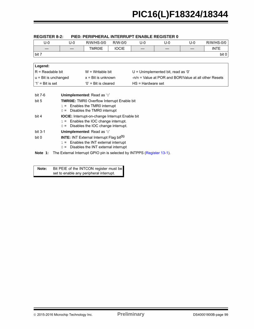
PIC16(L)F18324/18344
REGISTER 8-2: PIE0: PERIPHERAL INTERRUPT ENABLE REGISTER 0
U-0 U-0 R/W/HS-0/0 R/W-0/0 U-0 U-0 U-0 R/W/HS-0/0
— — TMR0IE IOCIE — — — INTE
bit 7 bit 0
Legend:
R = Readable bit W = Writable bit U = Unimplemented bit, read as ‘0’
u = Bit is unchanged x = Bit is unknown -n/n = Value at POR and BOR/Value at all other Resets
‘1’ = Bit is set ‘0’ = Bit is cleared HS = Hardware set
bit 7-6 Unimplemented: Read as ‘0’
bit 5 TMR0IE: TMR0 Overflow Interrupt Enable bit1 = Enables the TMR0 interrupt0 = Disables the TMR0 interrupt
bit 4 IOCIE: Interrupt-on-change Interrupt Enable bit1 = Enables the IOC change interrupt.0 = Disables the IOC change interrupt.
bit 3-1 Unimplemented: Read as ‘0’
bit 0 INTE: INT External Interrupt Flag bit(1)
1 = Enables the INT external interrupt0 = Disables the INT external interrupt
Note 1: The External Interrupt GPIO pin is selected by INTPPS (Register 13-1).
Note: Bit PEIE of the INTCON register must beset to enable any peripheral interrupt.
2015-2016 Microchip Technology Inc. Preliminary DS40001800B-page 99
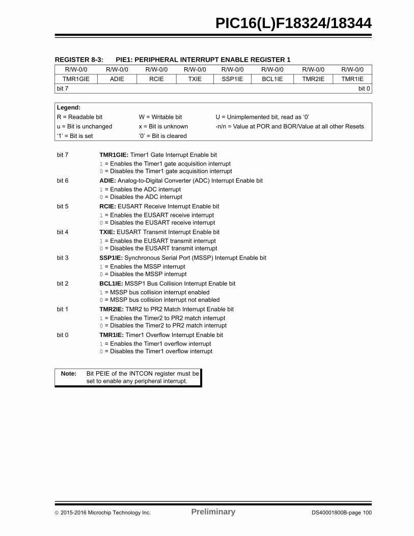
PIC16(L)F18324/18344
REGISTER 8-3: PIE1: PERIPHERAL INTERRUPT ENABLE REGISTER 1
R/W-0/0 R/W-0/0 R/W-0/0 R/W-0/0 R/W-0/0 R/W-0/0 R/W-0/0 R/W-0/0
TMR1GIE ADIE RCIE TXIE SSP1IE BCL1IE TMR2IE TMR1IE
bit 7 bit 0
Legend:
R = Readable bit W = Writable bit U = Unimplemented bit, read as ‘0’
u = Bit is unchanged x = Bit is unknown -n/n = Value at POR and BOR/Value at all other Resets
‘1’ = Bit is set ‘0’ = Bit is cleared
bit 7 TMR1GIE: Timer1 Gate Interrupt Enable bit
1 = Enables the Timer1 gate acquisition interrupt0 = Disables the Timer1 gate acquisition interrupt
bit 6 ADIE: Analog-to-Digital Converter (ADC) Interrupt Enable bit
1 = Enables the ADC interrupt0 = Disables the ADC interrupt
bit 5 RCIE: EUSART Receive Interrupt Enable bit
1 = Enables the EUSART receive interrupt0 = Disables the EUSART receive interrupt
bit 4 TXIE: EUSART Transmit Interrupt Enable bit
1 = Enables the EUSART transmit interrupt0 = Disables the EUSART transmit interrupt
bit 3 SSP1IE: Synchronous Serial Port (MSSP) Interrupt Enable bit
1 = Enables the MSSP interrupt0 = Disables the MSSP interrupt
bit 2 BCL1IE: MSSP1 Bus Collision Interrupt Enable bit
1 = MSSP bus collision interrupt enabled0 = MSSP bus collision interrupt not enabled
bit 1 TMR2IE: TMR2 to PR2 Match Interrupt Enable bit
1 = Enables the Timer2 to PR2 match interrupt0 = Disables the Timer2 to PR2 match interrupt
bit 0 TMR1IE: Timer1 Overflow Interrupt Enable bit
1 = Enables the Timer1 overflow interrupt0 = Disables the Timer1 overflow interrupt
Note: Bit PEIE of the INTCON register must beset to enable any peripheral interrupt.
2015-2016 Microchip Technology Inc. Preliminary DS40001800B-page 100
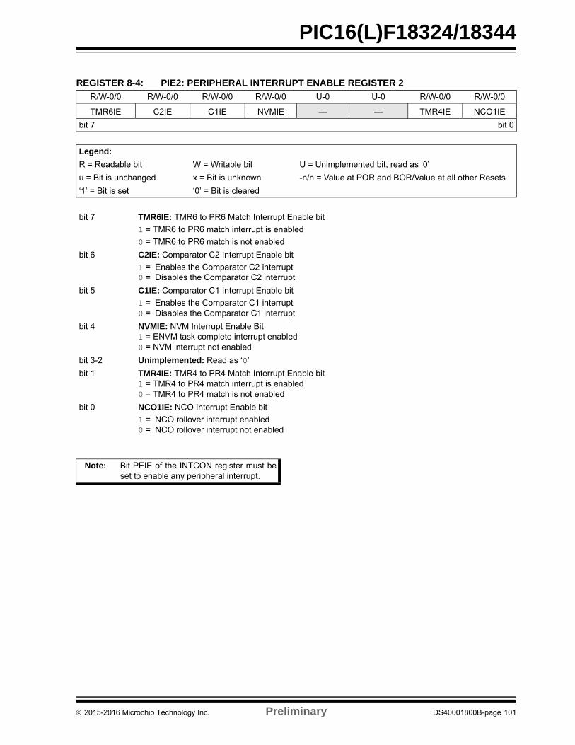
PIC16(L)F18324/18344
REGISTER 8-4: PIE2: PERIPHERAL INTERRUPT ENABLE REGISTER 2
R/W-0/0 R/W-0/0 R/W-0/0 R/W-0/0 U-0 U-0 R/W-0/0 R/W-0/0
TMR6IE C2IE C1IE NVMIE — — TMR4IE NCO1IE
bit 7 bit 0
Legend:
R = Readable bit W = Writable bit U = Unimplemented bit, read as ‘0’
u = Bit is unchanged x = Bit is unknown -n/n = Value at POR and BOR/Value at all other Resets
‘1’ = Bit is set ‘0’ = Bit is cleared
bit 7 TMR6IE: TMR6 to PR6 Match Interrupt Enable bit
1 = TMR6 to PR6 match interrupt is enabled
0 = TMR6 to PR6 match is not enabled
bit 6 C2IE: Comparator C2 Interrupt Enable bit
1 = Enables the Comparator C2 interrupt0 = Disables the Comparator C2 interrupt
bit 5 C1IE: Comparator C1 Interrupt Enable bit
1 = Enables the Comparator C1 interrupt0 = Disables the Comparator C1 interrupt
bit 4 NVMIE: NVM Interrupt Enable Bit1 = ENVM task complete interrupt enabled0 = NVM interrupt not enabled
bit 3-2 Unimplemented: Read as ‘0’
bit 1 TMR4IE: TMR4 to PR4 Match Interrupt Enable bit1 = TMR4 to PR4 match interrupt is enabled0 = TMR4 to PR4 match is not enabled
bit 0 NCO1IE: NCO Interrupt Enable bit
1 = NCO rollover interrupt enabled0 = NCO rollover interrupt not enabled
Note: Bit PEIE of the INTCON register must beset to enable any peripheral interrupt.
2015-2016 Microchip Technology Inc. Preliminary DS40001800B-page 101
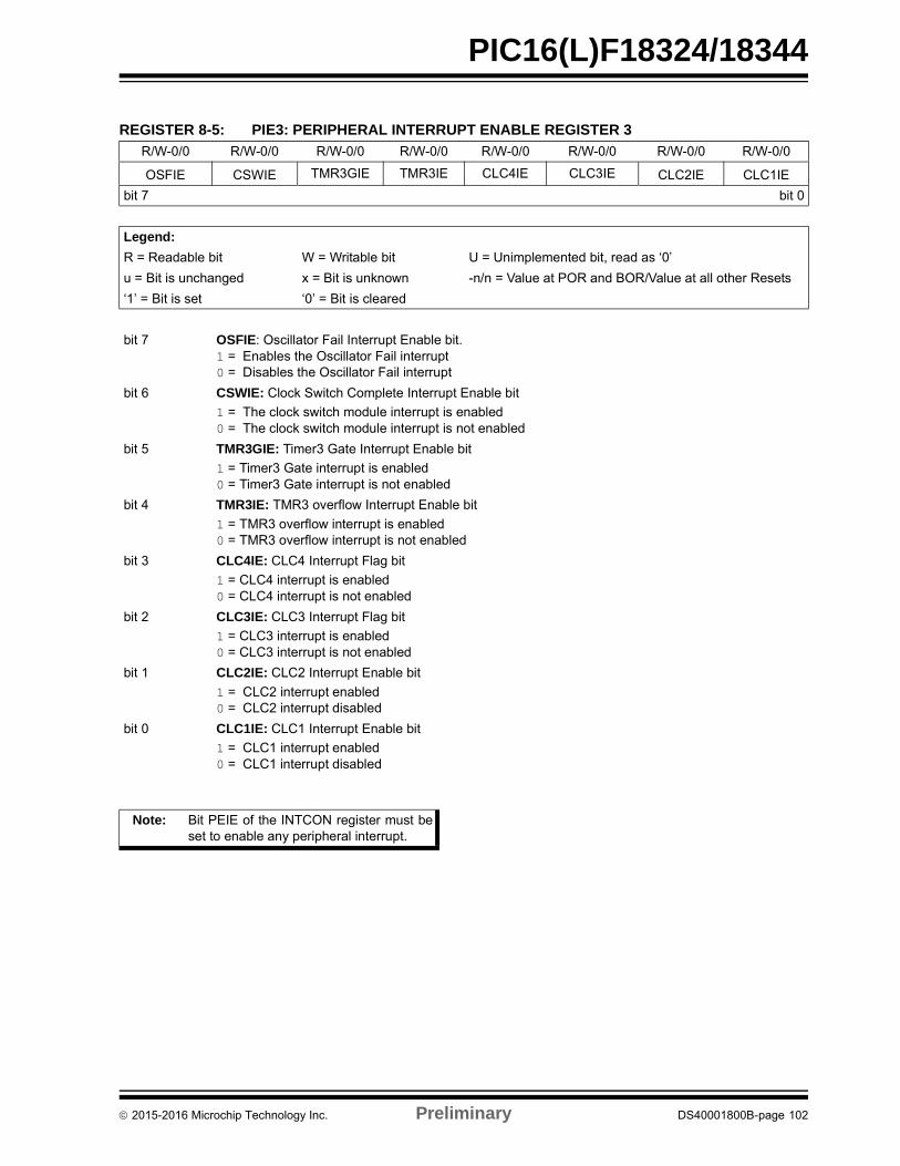
PIC16(L)F18324/18344
REGISTER 8-5: PIE3: PERIPHERAL INTERRUPT ENABLE REGISTER 3
R/W-0/0 R/W-0/0 R/W-0/0 R/W-0/0 R/W-0/0 R/W-0/0 R/W-0/0 R/W-0/0
OSFIE CSWIE TMR3GIE TMR3IE CLC4IE CLC3IE CLC2IE CLC1IE
bit 7 bit 0
Legend:
R = Readable bit W = Writable bit U = Unimplemented bit, read as ‘0’
u = Bit is unchanged x = Bit is unknown -n/n = Value at POR and BOR/Value at all other Resets
‘1’ = Bit is set ‘0’ = Bit is cleared
bit 7 OSFIE: Oscillator Fail Interrupt Enable bit.1 = Enables the Oscillator Fail interrupt0 = Disables the Oscillator Fail interrupt
bit 6 CSWIE: Clock Switch Complete Interrupt Enable bit
1 = The clock switch module interrupt is enabled0 = The clock switch module interrupt is not enabled
bit 5 TMR3GIE: Timer3 Gate Interrupt Enable bit
1 = Timer3 Gate interrupt is enabled0 = Timer3 Gate interrupt is not enabled
bit 4 TMR3IE: TMR3 overflow Interrupt Enable bit
1 = TMR3 overflow interrupt is enabled0 = TMR3 overflow interrupt is not enabled
bit 3 CLC4IE: CLC4 Interrupt Flag bit
1 = CLC4 interrupt is enabled0 = CLC4 interrupt is not enabled
bit 2 CLC3IE: CLC3 Interrupt Flag bit
1 = CLC3 interrupt is enabled0 = CLC3 interrupt is not enabled
bit 1 CLC2IE: CLC2 Interrupt Enable bit
1 = CLC2 interrupt enabled0 = CLC2 interrupt disabled
bit 0 CLC1IE: CLC1 Interrupt Enable bit
1 = CLC1 interrupt enabled0 = CLC1 interrupt disabled
Note: Bit PEIE of the INTCON register must beset to enable any peripheral interrupt.
2015-2016 Microchip Technology Inc. Preliminary DS40001800B-page 102
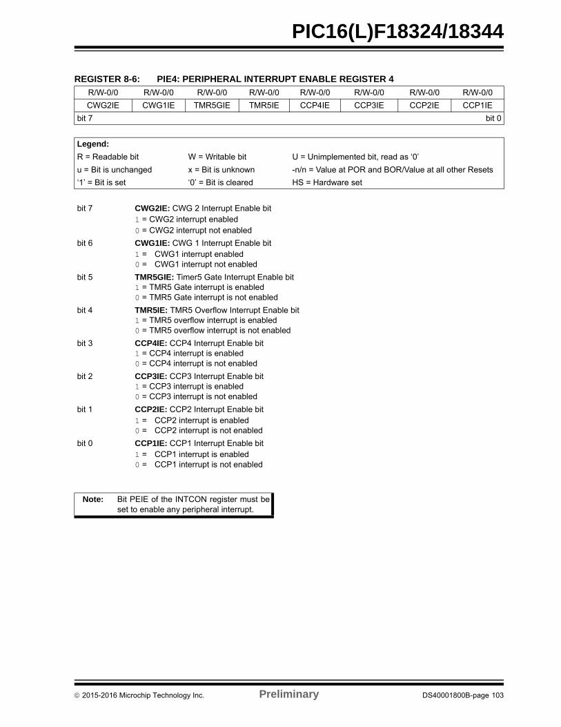
PIC16(L)F18324/18344
REGISTER 8-6: PIE4: PERIPHERAL INTERRUPT ENABLE REGISTER 4
R/W-0/0 R/W-0/0 R/W-0/0 R/W-0/0 R/W-0/0 R/W-0/0 R/W-0/0 R/W-0/0
CWG2IE CWG1IE TMR5GIE TMR5IE CCP4IE CCP3IE CCP2IE CCP1IE
bit 7 bit 0
Legend:
R = Readable bit W = Writable bit U = Unimplemented bit, read as ‘0’
u = Bit is unchanged x = Bit is unknown -n/n = Value at POR and BOR/Value at all other Resets
‘1’ = Bit is set ‘0’ = Bit is cleared HS = Hardware set
bit 7 CWG2IE: CWG 2 Interrupt Enable bit1 = CWG2 interrupt enabled0 = CWG2 interrupt not enabled
bit 6 CWG1IE: CWG 1 Interrupt Enable bit1 = CWG1 interrupt enabled0 = CWG1 interrupt not enabled
bit 5 TMR5GIE: Timer5 Gate Interrupt Enable bit1 = TMR5 Gate interrupt is enabled0 = TMR5 Gate interrupt is not enabled
bit 4 TMR5IE: TMR5 Overflow Interrupt Enable bit1 = TMR5 overflow interrupt is enabled0 = TMR5 overflow interrupt is not enabled
bit 3 CCP4IE: CCP4 Interrupt Enable bit1 = CCP4 interrupt is enabled0 = CCP4 interrupt is not enabled
bit 2 CCP3IE: CCP3 Interrupt Enable bit1 = CCP3 interrupt is enabled0 = CCP3 interrupt is not enabled
bit 1 CCP2IE: CCP2 Interrupt Enable bit1 = CCP2 interrupt is enabled0 = CCP2 interrupt is not enabled
bit 0 CCP1IE: CCP1 Interrupt Enable bit1 = CCP1 interrupt is enabled0 = CCP1 interrupt is not enabled
Note: Bit PEIE of the INTCON register must beset to enable any peripheral interrupt.
2015-2016 Microchip Technology Inc. Preliminary DS40001800B-page 103
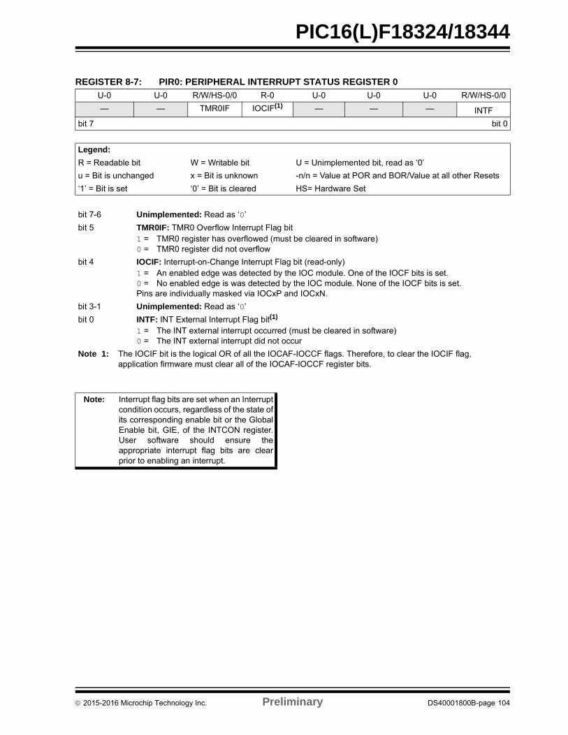
PIC16(L)F18324/18344
REGISTER 8-7: PIR0: PERIPHERAL INTERRUPT STATUS REGISTER 0
U-0 U-0 R/W/HS-0/0 R-0 U-0 U-0 U-0 R/W/HS-0/0
— — TMR0IF IOCIF(1) — — — INTF
bit 7 bit 0
Legend:
R = Readable bit W = Writable bit U = Unimplemented bit, read as ‘0’
u = Bit is unchanged x = Bit is unknown -n/n = Value at POR and BOR/Value at all other Resets
‘1’ = Bit is set ‘0’ = Bit is cleared HS= Hardware Set
bit 7-6 Unimplemented: Read as ‘0’
bit 5 TMR0IF: TMR0 Overflow Interrupt Flag bit1 = TMR0 register has overflowed (must be cleared in software)0 = TMR0 register did not overflow
bit 4 IOCIF: Interrupt-on-Change Interrupt Flag bit (read-only)1 = An enabled edge was detected by the IOC module. One of the IOCF bits is set.0 = No enabled edge is was detected by the IOC module. None of the IOCF bits is set.Pins are individually masked via IOCxP and IOCxN.
bit 3-1 Unimplemented: Read as ‘0’
bit 0 INTF: INT External Interrupt Flag bit(1)
1 = The INT external interrupt occurred (must be cleared in software)0 = The INT external interrupt did not occur
Note 1: The IOCIF bit is the logical OR of all the IOCAF-IOCCF flags. Therefore, to clear the IOCIF flag, application firmware must clear all of the IOCAF-IOCCF register bits.
Note: Interrupt flag bits are set when an Interruptcondition occurs, regardless of the state ofits corresponding enable bit or the GlobalEnable bit, GIE, of the INTCON register.User software should ensure theappropriate interrupt flag bits are clearprior to enabling an interrupt.
2015-2016 Microchip Technology Inc. Preliminary DS40001800B-page 104
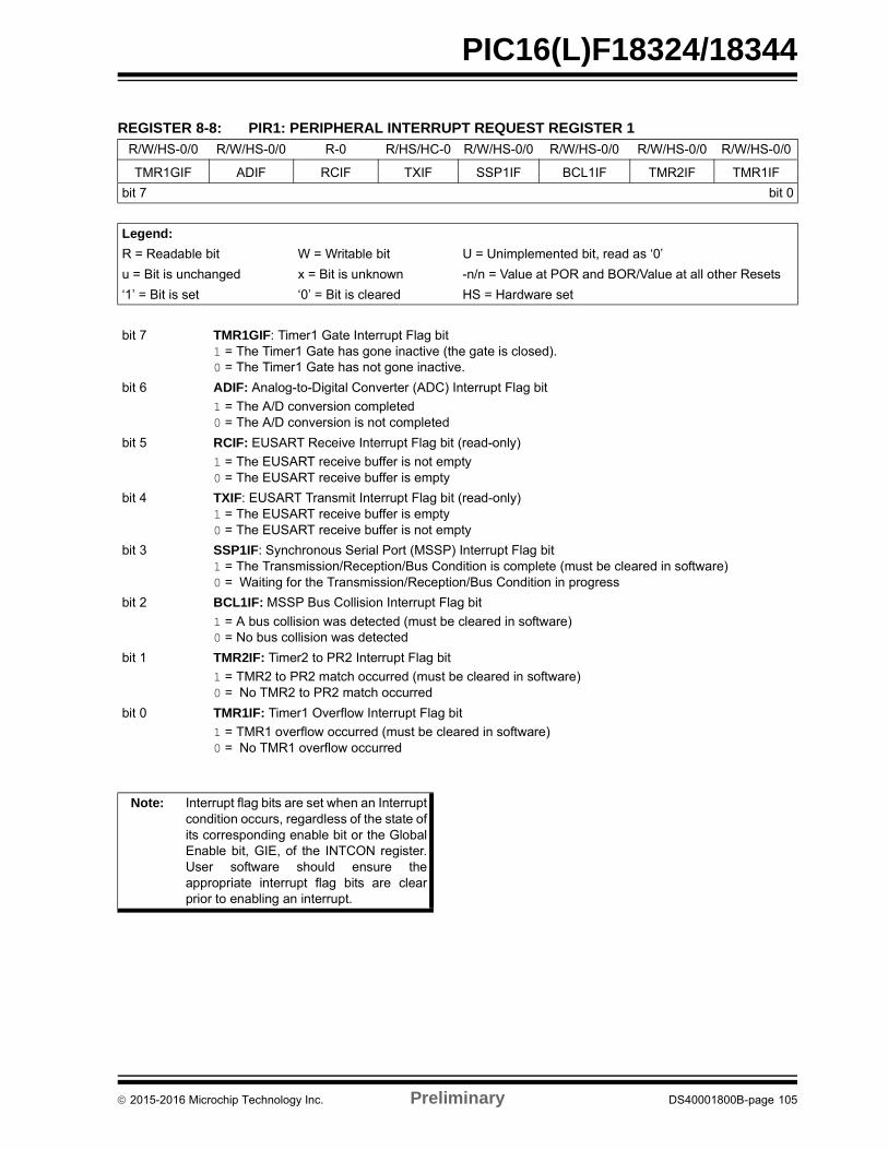
PIC16(L)F18324/18344
REGISTER 8-8: PIR1: PERIPHERAL INTERRUPT REQUEST REGISTER 1
R/W/HS-0/0 R/W/HS-0/0 R-0 R/HS/HC-0 R/W/HS-0/0 R/W/HS-0/0 R/W/HS-0/0 R/W/HS-0/0
TMR1GIF ADIF RCIF TXIF SSP1IF BCL1IF TMR2IF TMR1IF
bit 7 bit 0
Legend:
R = Readable bit W = Writable bit U = Unimplemented bit, read as ‘0’
u = Bit is unchanged x = Bit is unknown -n/n = Value at POR and BOR/Value at all other Resets
‘1’ = Bit is set ‘0’ = Bit is cleared HS = Hardware set
bit 7 TMR1GIF: Timer1 Gate Interrupt Flag bit1 = The Timer1 Gate has gone inactive (the gate is closed).0 = The Timer1 Gate has not gone inactive.
bit 6 ADIF: Analog-to-Digital Converter (ADC) Interrupt Flag bit
1 = The A/D conversion completed0 = The A/D conversion is not completed
bit 5 RCIF: EUSART Receive Interrupt Flag bit (read-only)
1 = The EUSART receive buffer is not empty0 = The EUSART receive buffer is empty
bit 4 TXIF: EUSART Transmit Interrupt Flag bit (read-only)1 = The EUSART receive buffer is empty0 = The EUSART receive buffer is not empty
bit 3 SSP1IF: Synchronous Serial Port (MSSP) Interrupt Flag bit1 = The Transmission/Reception/Bus Condition is complete (must be cleared in software)0 = Waiting for the Transmission/Reception/Bus Condition in progress
bit 2 BCL1IF: MSSP Bus Collision Interrupt Flag bit
1 = A bus collision was detected (must be cleared in software)0 = No bus collision was detected
bit 1 TMR2IF: Timer2 to PR2 Interrupt Flag bit
1 = TMR2 to PR2 match occurred (must be cleared in software)0 = No TMR2 to PR2 match occurred
bit 0 TMR1IF: Timer1 Overflow Interrupt Flag bit
1 = TMR1 overflow occurred (must be cleared in software)0 = No TMR1 overflow occurred
Note: Interrupt flag bits are set when an Interruptcondition occurs, regardless of the state ofits corresponding enable bit or the GlobalEnable bit, GIE, of the INTCON register.User software should ensure theappropriate interrupt flag bits are clearprior to enabling an interrupt.
2015-2016 Microchip Technology Inc. Preliminary DS40001800B-page 105
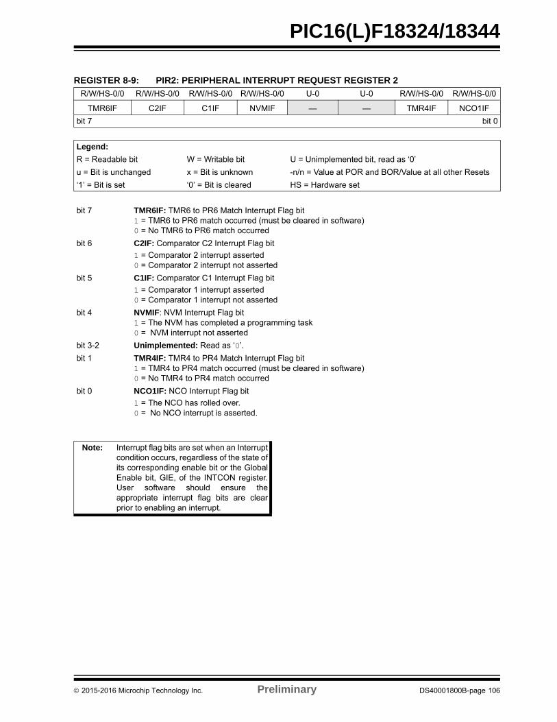
PIC16(L)F18324/18344
REGISTER 8-9: PIR2: PERIPHERAL INTERRUPT REQUEST REGISTER 2
R/W/HS-0/0 R/W/HS-0/0 R/W/HS-0/0 R/W/HS-0/0 U-0 U-0 R/W/HS-0/0 R/W/HS-0/0
TMR6IF C2IF C1IF NVMIF — — TMR4IF NCO1IF
bit 7 bit 0
Legend:
R = Readable bit W = Writable bit U = Unimplemented bit, read as ‘0’
u = Bit is unchanged x = Bit is unknown -n/n = Value at POR and BOR/Value at all other Resets
‘1’ = Bit is set ‘0’ = Bit is cleared HS = Hardware set
bit 7 TMR6IF: TMR6 to PR6 Match Interrupt Flag bit1 = TMR6 to PR6 match occurred (must be cleared in software)0 = No TMR6 to PR6 match occurred
bit 6 C2IF: Comparator C2 Interrupt Flag bit
1 = Comparator 2 interrupt asserted0 = Comparator 2 interrupt not asserted
bit 5 C1IF: Comparator C1 Interrupt Flag bit
1 = Comparator 1 interrupt asserted0 = Comparator 1 interrupt not asserted
bit 4 NVMIF: NVM Interrupt Flag bit1 = The NVM has completed a programming task0 = NVM interrupt not asserted
bit 3-2 Unimplemented: Read as ‘0’.
bit 1 TMR4IF: TMR4 to PR4 Match Interrupt Flag bit1 = TMR4 to PR4 match occurred (must be cleared in software)0 = No TMR4 to PR4 match occurred
bit 0 NCO1IF: NCO Interrupt Flag bit
1 = The NCO has rolled over.0 = No NCO interrupt is asserted.
Note: Interrupt flag bits are set when an Interruptcondition occurs, regardless of the state ofits corresponding enable bit or the GlobalEnable bit, GIE, of the INTCON register.User software should ensure theappropriate interrupt flag bits are clearprior to enabling an interrupt.
2015-2016 Microchip Technology Inc. Preliminary DS40001800B-page 106
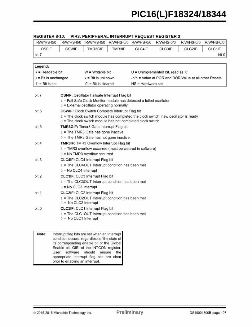
PIC16(L)F18324/18344
REGISTER 8-10: PIR3: PERIPHERAL INTERRUPT REQUEST REGISTER 3
R/W/HS-0/0 R/W/HS-0/0 R/W/HS-0/0 R/W/HS-0/0 R/W/HS-0/0 R/W/HS-0/0 R/W/HS-0/0 R/W/HS-0/0
OSFIF CSWIF TMR3GIF TMR3IF CLC4IF CLC3IF CLC2IF CLC1IF
bit 7 bit 0
Legend:
R = Readable bit W = Writable bit U = Unimplemented bit, read as ‘0’
u = Bit is unchanged x = Bit is unknown -n/n = Value at POR and BOR/Value at all other Resets
‘1’ = Bit is set ‘0’ = Bit is cleared HS = Hardware set
bit 7 OSFIF: Oscillator Failsafe Interrupt Flag bit
1 = Fail-Safe Clock Monitor module has detected a failed oscillator0 = External oscillator operating normally
bit 6 CSWIF: Clock Switch Complete Interrupt Flag bit
1 = The clock switch module has completed the clock switch; new oscillator is ready0 = The clock switch module has not completed clock switch
bit 5 TMR3GIF: Timer3 Gate Interrupt Flag bit
1 = The TMR3 Gate has gone inactive
0 = The TMR3 Gate has not gone inactive.
bit 4 TMR3IF: TMR3 Overflow Interrupt Flag bit
1 = TMR3 overflow occurred (must be cleared in software)
0 = No TMR3 overflow occurred
bit 3 CLC4IF: CLC4 Interrupt Flag bit
1 = The CLC4OUT Interrupt condition has been met
0 = No CLC4 Interrupt
bit 2 CLC3IF: CLC3 Interrupt Flag bit
1 = The CLC3OUT Interrupt condition has been met
0 = No CLC3 Interrupt
bit 1 CLC2IF: CLC2 Interrupt Flag bit
1 = The CLC2OUT Interrupt condition has been met0 = No CLC2 Interrupt
bit 0 CLC1IF: CLC1 Interrupt Flag bit
1 = The CLC1OUT Interrupt condition has been met0 = No CLC1 Interrupt
Note: Interrupt flag bits are set when an Interruptcondition occurs, regardless of the state ofits corresponding enable bit or the GlobalEnable bit, GIE, of the INTCON register.User software should ensure theappropriate interrupt flag bits are clearprior to enabling an interrupt.
2015-2016 Microchip Technology Inc. Preliminary DS40001800B-page 107
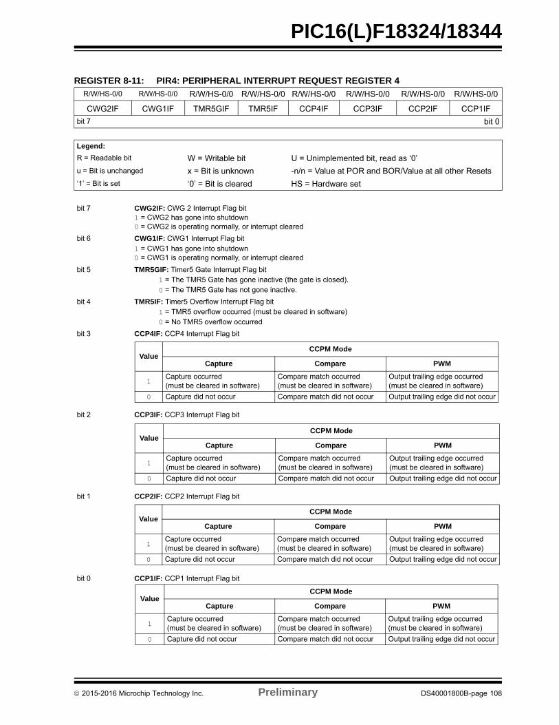
PIC16(L)F18324/18344
REGISTER 8-11: PIR4: PERIPHERAL INTERRUPT REQUEST REGISTER 4R/W/HS-0/0 R/W/HS-0/0 R/W/HS-0/0 R/W/HS-0/0 R/W/HS-0/0 R/W/HS-0/0 R/W/HS-0/0 R/W/HS-0/0
CWG2IF CWG1IF TMR5GIF TMR5IF CCP4IF CCP3IF CCP2IF CCP1IF
bit 7 bit 0
Legend:
R = Readable bit W = Writable bit U = Unimplemented bit, read as ‘0’
u = Bit is unchanged x = Bit is unknown -n/n = Value at POR and BOR/Value at all other Resets
‘1’ = Bit is set ‘0’ = Bit is cleared HS = Hardware set
bit 7 CWG2IF: CWG 2 Interrupt Flag bit1 = CWG2 has gone into shutdown0 = CWG2 is operating normally, or interrupt cleared
bit 6 CWG1IF: CWG1 Interrupt Flag bit1 = CWG1 has gone into shutdown0 = CWG1 is operating normally, or interrupt cleared
bit 5 TMR5GIF: Timer5 Gate Interrupt Flag bit 1 = The TMR5 Gate has gone inactive (the gate is closed). 0 = The TMR5 Gate has not gone inactive.
bit 4 TMR5IF: Timer5 Overflow Interrupt Flag bit 1 = TMR5 overflow occurred (must be cleared in software) 0 = No TMR5 overflow occurred
bit 3 CCP4IF: CCP4 Interrupt Flag bit
bit 2 CCP3IF: CCP3 Interrupt Flag bit
bit 1 CCP2IF: CCP2 Interrupt Flag bit
bit 0 CCP1IF: CCP1 Interrupt Flag bit
ValueCCPM Mode
Capture Compare PWM
1Capture occurred(must be cleared in software)
Compare match occurred(must be cleared in software)
Output trailing edge occurred(must be cleared in software)
0 Capture did not occur Compare match did not occur Output trailing edge did not occur
ValueCCPM Mode
Capture Compare PWM
1Capture occurred(must be cleared in software)
Compare match occurred(must be cleared in software)
Output trailing edge occurred(must be cleared in software)
0 Capture did not occur Compare match did not occur Output trailing edge did not occur
ValueCCPM Mode
Capture Compare PWM
1Capture occurred(must be cleared in software)
Compare match occurred(must be cleared in software)
Output trailing edge occurred(must be cleared in software)
0 Capture did not occur Compare match did not occur Output trailing edge did not occur
ValueCCPM Mode
Capture Compare PWM
1Capture occurred(must be cleared in software)
Compare match occurred(must be cleared in software)
Output trailing edge occurred(must be cleared in software)
0 Capture did not occur Compare match did not occur Output trailing edge did not occur
2015-2016 Microchip Technology Inc. Preliminary DS40001800B-page 108
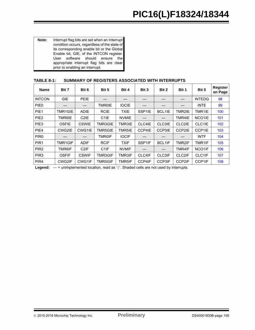
PIC16(L)F18324/18344
Note: Interrupt flag bits are set when an Interruptcondition occurs, regardless of the state ofits corresponding enable bit or the GlobalEnable bit, GIE, of the INTCON register.User software should ensure theappropriate interrupt flag bits are clearprior to enabling an interrupt.
TABLE 8-1: SUMMARY OF REGISTERS ASSOCIATED WITH INTERRUPTS
Name Bit 7 Bit 6 Bit 5 Bit 4 Bit 3 Bit 2 Bit 1 Bit 0Register on Page
INTCON GIE PEIE — — — — — INTEDG 98
PIE0 — — TMR0IE IOCIE — — — INTE 99
PIE1 TMR1GIE ADIE RCIE TXIE SSP1IE BCL1IE TMR2IE TMR1IE 100
PIE2 TMR6IE C2IE C1IE NVMIE — — TMR4IE NCO1IE 101
PIE3 OSFIE CSWIE TMR3GIE TMR3IE CLC4IE CLC3IE CLC2IE CLC1IE 102
PIE4 CWG2IE CWG1IE TMR5GIE TMR5IE CCP4IE CCP3IE CCP2IE CCP1IE 103
PIR0 — — TMR0IF IOCIF — — — INTF 104
PIR1 TMR1GIF ADIF RCIF TXIF SSP1IF BCL1IF TMR2IF TMR1IF 105
PIR2 TMR6IF C2IF C1IF NVMIF — — TMR4IF NCO1IF 106
PIR3 OSFIF CSWIF TMR3GIF TMR3IF CLC4IF CLC3IF CLC2IF CLC1IF 107
PIR4 CWG2IF CWG1IF TMR5GIF TMR5IF CCP4IF CCP3IF CCP2IF CCP1IF 108
Legend: — = unimplemented location, read as ‘0’. Shaded cells are not used by interrupts.
2015-2016 Microchip Technology Inc. Preliminary DS40001800B-page 109
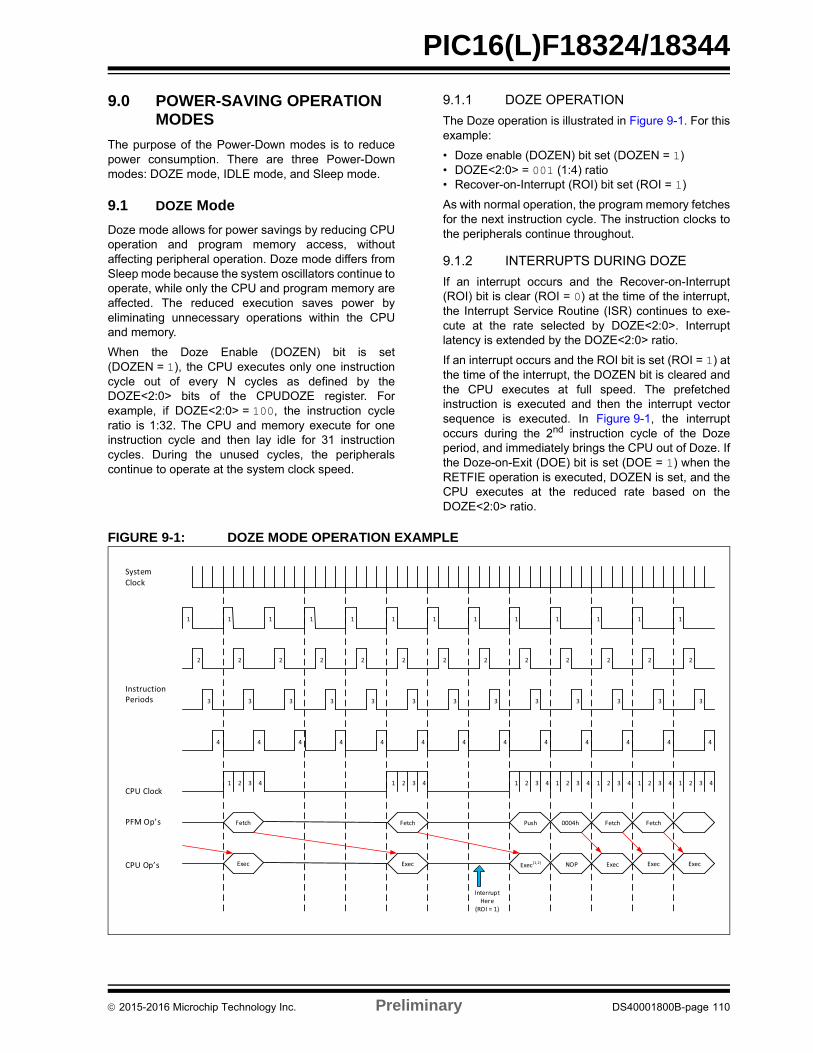
PIC16(L)F18324/18344
9.0 POWER-SAVING OPERATION MODES
The purpose of the Power-Down modes is to reducepower consumption. There are three Power-Downmodes: DOZE mode, IDLE mode, and Sleep mode.
9.1 DOZE Mode
Doze mode allows for power savings by reducing CPUoperation and program memory access, withoutaffecting peripheral operation. Doze mode differs fromSleep mode because the system oscillators continue tooperate, while only the CPU and program memory areaffected. The reduced execution saves power byeliminating unnecessary operations within the CPUand memory.
When the Doze Enable (DOZEN) bit is set(DOZEN = 1), the CPU executes only one instructioncycle out of every N cycles as defined by theDOZE<2:0> bits of the CPUDOZE register. Forexample, if DOZE<2:0> = 100, the instruction cycleratio is 1:32. The CPU and memory execute for oneinstruction cycle and then lay idle for 31 instructioncycles. During the unused cycles, the peripheralscontinue to operate at the system clock speed.
9.1.1 DOZE OPERATION
The Doze operation is illustrated in Figure 9-1. For thisexample:
• Doze enable (DOZEN) bit set (DOZEN = 1)• DOZE<2:0> = 001 (1:4) ratio• Recover-on-Interrupt (ROI) bit set (ROI = 1)
As with normal operation, the program memory fetchesfor the next instruction cycle. The instruction clocks tothe peripherals continue throughout.
9.1.2 INTERRUPTS DURING DOZE
If an interrupt occurs and the Recover-on-Interrupt(ROI) bit is clear (ROI = 0) at the time of the interrupt,the Interrupt Service Routine (ISR) continues to exe-cute at the rate selected by DOZE<2:0>. Interruptlatency is extended by the DOZE<2:0> ratio.
If an interrupt occurs and the ROI bit is set (ROI = 1) atthe time of the interrupt, the DOZEN bit is cleared andthe CPU executes at full speed. The prefetchedinstruction is executed and then the interrupt vectorsequence is executed. In Figure 9-1, the interruptoccurs during the 2nd instruction cycle of the Dozeperiod, and immediately brings the CPU out of Doze. Ifthe Doze-on-Exit (DOE) bit is set (DOE = 1) when theRETFIE operation is executed, DOZEN is set, and theCPU executes at the reduced rate based on theDOZE<2:0> ratio.
FIGURE 9-1: DOZE MODE OPERATION EXAMPLE
System Clock
CPU Clock
PFM Op’s
CPU Op’s
1 1 1 1 1 1 1 1 1 1 1 1 1
1 2 3 4 2 2 2 2 2 2
2 2 22 22 2 2 2 2 2 2
1 1 1 1 1 13 3 3 3 3 34 4 4 4 4 4
2
3 3 3 3 3 3 3 3 3 3 3 3 3
4444444444444
Fetch Fetch FetchFetch
Exec Exec Exec(1,2) Exec Exec Exec
Push
NOP
0004h
Interrupt Here
(ROI = 1)
2015-2016 Microchip Technology Inc. Preliminary DS40001800B-page 110
PIC16(L)F18324/18344
9.2 IDLE Mode
When the IDLE Enable (IDLEN) bit is clear(IDLEN = 0), the SLEEP instruction will put the deviceinto full Sleep mode (see Section 9.3 “Sleep Mode”).When IDLEN is set (IDLEN = 1), the SLEEP instructionwill put the device into IDLE mode. In IDLE mode, theCPU and memory operations are halted, but theperipheral clocks continue to run. This mode is similarto DOZE mode, except that in IDLE both the CPU andprogram memory are shut off.
9.2.0.1 IDLE and Interrupts
IDLE mode ends when an interrupt occurs (even ifGIE = 0), but IDLEN is not changed. The device canre-enter IDLE by executing the SLEEP instruction.
If Recover-on-Interrupt is enabled (ROI = 1), theinterrupt that brings the device out of IDLE alsorestores full-speed CPU execution when DOZE is alsoenabled.
9.2.0.2 IDLE and WDT
When in IDLE, the WDT Reset is blocked and willinstead wake the device. The WDT wake-up is not aninterrupt, therefore ROI does not apply.
9.3 Sleep Mode
Sleep mode is entered by executing the SLEEPinstruction, while the Idle Enable (IDLEN) bit of theCPUDOZE register is clear (IDLEN = 0). If the SLEEPinstruction is executed while the IDLEN bit is set(IDLEN = 1), the CPU will enter the Idle mode(Section 9.3.3 “Low Power Sleep Mode”).
Upon entering Sleep mode, the following conditionsexist:
1. Resets other than WDT are not affected bySleep mode; WDT will be cleared but keepsrunning if enabled for operation during Sleep
2. The PD bit of the STATUS register is cleared
3. The TO bit of the STATUS register is set
4. The CPU and System clocks are disabled5. 31 kHz LFINTOSC, HFINTOSC and SOSC will
remain enabled if any peripheral has requestedthem as a clock source or if the HFOEN,LFOEN, or SOSCEN bits of the OSCEN registerare set.
6. ADC is unaffected if the dedicated ADCRCoscillator is selected. When the ADC clocksource is something other than ADCRC, aSLEEP instruction causes the presentconversion to be aborted and the ADC moduleis turned off, although the ADON bit remains set.
7. I/O ports maintain the status they had beforeSLEEP was executed (driving high, low, orhigh-impedance) only if no peripheral connectedto the I/O port is active.
Refer to individual chapters for more details onperipheral operation during Sleep.
To minimize current consumption, the followingconditions should be considered:
- I/O pins should not be floating- External circuitry sinking current from I/O pins- Internal circuitry sourcing current from I/O
pins- Current draw from pins with internal weak
pull-ups- Modules using any oscillator
I/O pins that are high-impedance inputs should bepulled to VDD or VSS externally to avoid switchingcurrents caused by floating inputs.
Examples of internal circuitry that might be sourcingcurrent include modules such as the DAC and FVRmodules. See Section 24.0 “5-Bit Digital-to-AnalogConverter (DAC1) Module” and Section 16.0 “FixedVoltage Reference (FVR)” for more information onthese modules.
Note: Peripherals using FOSC will continuerunning while in IDLE (but not in SLEEP).Peripherals using HFINTOSC,LFINTOSC, or SOSC will continueoperation in both IDLE and SLEEP.
Note: If CLKOUT is enabled (CLKOUT = 0,Configuration Word 1), the output willcontinue operating while in IDLE.
Note: The WDT can bring the device out ofIDLE, in the same way it brings the deviceout of Sleep. The DOZEN bit is notaffected.
2015-2016 Microchip Technology Inc. Preliminary DS40001800B-page 111
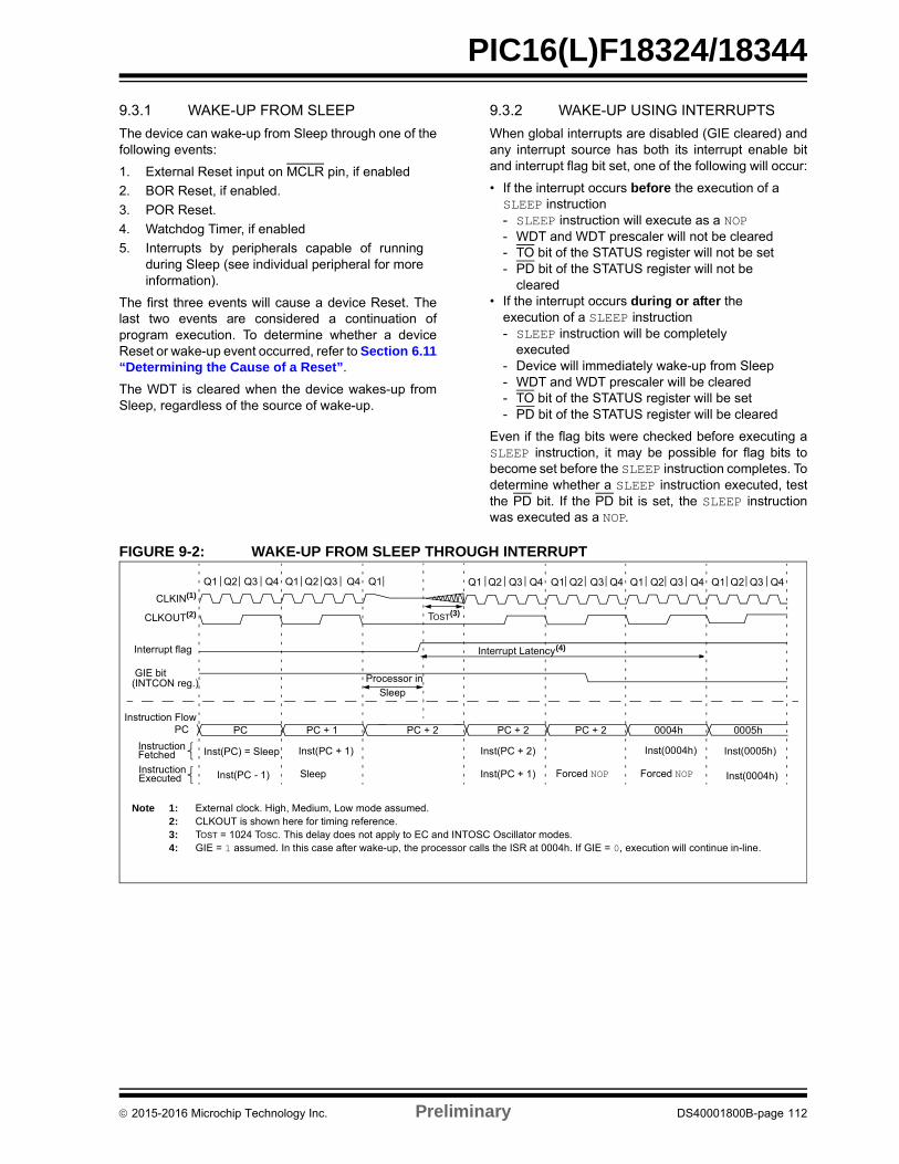
PIC16(L)F18324/18344
9.3.1 WAKE-UP FROM SLEEP
The device can wake-up from Sleep through one of thefollowing events:
1. External Reset input on MCLR pin, if enabled
2. BOR Reset, if enabled.
3. POR Reset.
4. Watchdog Timer, if enabled
5. Interrupts by peripherals capable of runningduring Sleep (see individual peripheral for moreinformation).
The first three events will cause a device Reset. Thelast two events are considered a continuation ofprogram execution. To determine whether a deviceReset or wake-up event occurred, refer to Section 6.11“Determining the Cause of a Reset”.
The WDT is cleared when the device wakes-up fromSleep, regardless of the source of wake-up.
9.3.2 WAKE-UP USING INTERRUPTS
When global interrupts are disabled (GIE cleared) andany interrupt source has both its interrupt enable bitand interrupt flag bit set, one of the following will occur:
• If the interrupt occurs before the execution of a SLEEP instruction- SLEEP instruction will execute as a NOP- WDT and WDT prescaler will not be cleared- TO bit of the STATUS register will not be set- PD bit of the STATUS register will not be
cleared• If the interrupt occurs during or after the
execution of a SLEEP instruction- SLEEP instruction will be completely
executed- Device will immediately wake-up from Sleep- WDT and WDT prescaler will be cleared- TO bit of the STATUS register will be set- PD bit of the STATUS register will be cleared
Even if the flag bits were checked before executing aSLEEP instruction, it may be possible for flag bits tobecome set before the SLEEP instruction completes. Todetermine whether a SLEEP instruction executed, testthe PD bit. If the PD bit is set, the SLEEP instructionwas executed as a NOP.
FIGURE 9-2: WAKE-UP FROM SLEEP THROUGH INTERRUPT
Q1 Q2 Q3 Q4 Q1 Q2 Q3 Q4 Q1 Q1 Q2 Q3 Q4 Q1 Q2 Q3 Q4 Q1 Q2 Q3 Q4 Q1 Q2 Q3 Q4
CLKIN(1)
CLKOUT(2)
Interrupt flag
GIE bit(INTCON reg.)
Instruction FlowPC
InstructionFetched
InstructionExecuted
PC PC + 1 PC + 2
Inst(PC) = Sleep
Inst(PC - 1)
Inst(PC + 1)
Sleep
Processor inSleep
Interrupt Latency(4)
Inst(PC + 2)
Inst(PC + 1)
Inst(0004h) Inst(0005h)
Inst(0004h)Forced NOP
PC + 2 0004h 0005h
Forced NOP
TOST(3)
PC + 2
Note 1: External clock. High, Medium, Low mode assumed.2: CLKOUT is shown here for timing reference.3: TOST = 1024 TOSC. This delay does not apply to EC and INTOSC Oscillator modes.4: GIE = 1 assumed. In this case after wake-up, the processor calls the ISR at 0004h. If GIE = 0, execution will continue in-line.
2015-2016 Microchip Technology Inc. Preliminary DS40001800B-page 112
PIC16(L)F18324/18344
9.3.3 LOW POWER SLEEP MODE
The PIC16F18324/18344 device contains an internalLow Dropout (LDO) voltage regulator, which allows thedevice I/O pins to operate at voltages up to 5.5V whilethe internal device logic operates at a lower voltage.The LDO and its associated reference circuitry mustremain active when the device is in Sleep mode.
The PIC16F18324/18344 allows the user to optimizethe operating current in Sleep, depending on theapplication requirements.
Low-Power Sleep mode can be selected by setting theVREGPM bit of the VREGCON register. Depending onthe configuration of this bit, the LDO and referencecircuitry are placed in a low-power state when thedevice is in Sleep.
9.3.3.1 Sleep Current vs. Wake-up Time
In the default operating mode, the LDO and referencecircuitry remain in the normal configuration while inSleep. The device is able to exit Sleep mode quicklysince all circuits remain active. In Low-Power Sleepmode, when waking-up from Sleep, an extra delay timeis required for these circuits to return to the normalconfiguration and stabilize.
The Low-Power Sleep mode is beneficial forapplications that stay in Sleep mode for long periods oftime. The Normal mode is beneficial for applicationsthat need to wake from Sleep quickly and frequently.
9.3.3.2 Peripheral Usage in Sleep
Some peripherals that can operate in Sleep mode willnot operate properly with the Low-Power Sleep modeselected. The Low-Power Sleep mode is intended foruse with these peripherals:
• Brown-out Reset (BOR)• Watchdog Timer (WDT)• External interrupt pin/Interrupt-on-change pins• Timer1 (with external clock source)
It is the responsibility of the end user to determine whatis acceptable for their application when setting theVREGPM settings in order to ensure operation inSleep.
Note: The PIC16LF18324/18344 does not havea configurable Low-Power Sleep mode.PIC16LF18324/18344 is an unregulateddevice and is always in the lowest powerstate when in Sleep, with no wake-up timepenalty. This device has a lower maximumVDD and I/O voltage than thePIC16F18324/18344. See Section 35.0“Electrical Specifications” for moreinformation.
2015-2016 Microchip Technology Inc. Preliminary DS40001800B-page 113
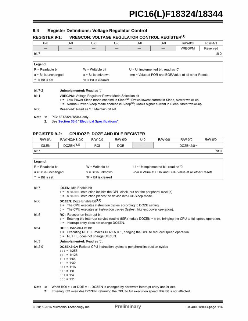
PIC16(L)F18324/18344
9.4 Register Definitions: Voltage Regulator Control
REGISTER 9-1: VREGCON: VOLTAGE REGULATOR CONTROL REGISTER(1) U-0 U-0 U-0 U-0 U-0 U-0 R/W-0/0 R/W-1/1
— — — — — — VREGPM Reserved
bit 7 bit 0
Legend:
R = Readable bit W = Writable bit U = Unimplemented bit, read as ‘0’
u = Bit is unchanged x = Bit is unknown -n/n = Value at POR and BOR/Value at all other Resets
‘1’ = Bit is set ‘0’ = Bit is cleared
bit 7-2 Unimplemented: Read as ‘0’
bit 1 VREGPM: Voltage Regulator Power Mode Selection bit1 = Low-Power Sleep mode enabled in Sleep(2); Draws lowest current in Sleep, slower wake-up0 = Normal-Power Sleep mode enabled in Sleep(2); Draws higher current in Sleep, faster wake-up
bit 0 Reserved: Read as ‘1’. Maintain bit set.
Note 1: PIC16F18324/18344 only.2: See Section 35.0 “Electrical Specifications”.
REGISTER 9-2: CPUDOZE: DOZE AND IDLE REGISTERR/W-0/u R/W/HC/HS-0/0 R/W-0/0 R/W-0/0 U-0 R/W-0/0 R/W-0/0 R/W-0/0
IDLEN DOZEN(1,2) ROI DOE — DOZE<2:0>
bit 7 bit 0
Legend:
R = Readable bit W = Writable bit U = Unimplemented bit, read as ‘0’
u = Bit is unchanged x = Bit is unknown -n/n = Value at POR and BOR/Value at all other Resets
‘1’ = Bit is set ‘0’ = Bit is cleared
bit 7 IDLEN: Idle Enable bit1 = A SLEEP instruction inhibits the CPU clock, but not the peripheral clock(s)0 = A SLEEP instruction places the device into Full-Sleep mode.
bit 6 DOZEN: Doze Enable bit(1,2)
1 = The CPU executes instruction cycles according to DOZE setting.0 = The CPU executes all instruction cycles (fastest, highest power operation).
bit 5 ROI: Recover-on-interrupt bit1 = Entering the interrupt service routine (ISR) makes DOZEN = 0 bit, bringing the CPU to full-speed operation.0 = Interrupt entry does not change DOZEN.
bit 4 DOE: Doze-on-Exit bit1 = Executing RETFIE makes DOZEN = 1, bringing the CPU to reduced speed operation.0 = RETFIE does not change DOZEN.
bit 3 Unimplemented: Read as ‘0’.
bit 2-0 DOZE<2:0>: Ratio of CPU instruction cycles to peripheral instruction cycles111 = 1:256110 = 1:128101 = 1:64100 = 1:32011 = 1:16010 = 1:8001 = 1:4000 = 1:2
Note 1: When ROI = 1 or DOE = 1, DOZEN is changed by hardware interrupt entry and/or exit.2: Entering ICD overrides DOZEN, returning the CPU to full execution speed; this bit is not affected.
2015-2016 Microchip Technology Inc. Preliminary DS40001800B-page 114
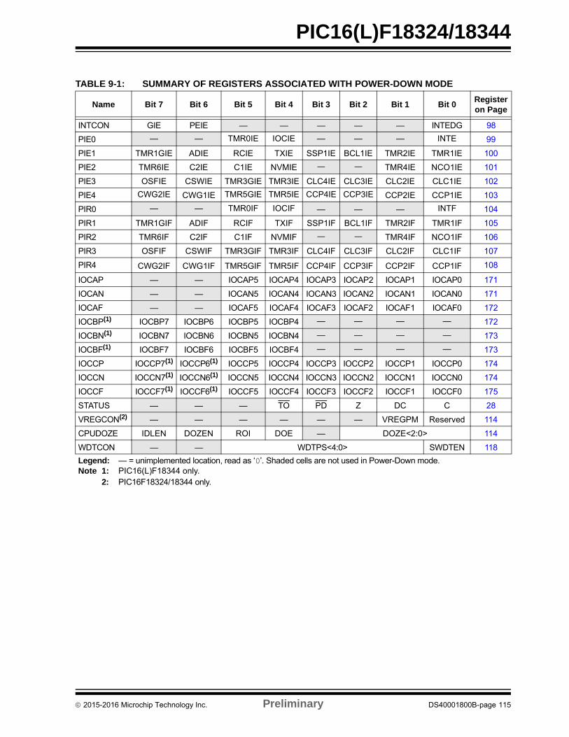
PIC16(L)F18324/18344
TABLE 9-1: SUMMARY OF REGISTERS ASSOCIATED WITH POWER-DOWN MODE
Name Bit 7 Bit 6 Bit 5 Bit 4 Bit 3 Bit 2 Bit 1 Bit 0Register on Page
INTCON GIE PEIE — — — — — INTEDG 98
PIE0 — — TMR0IE IOCIE — — — INTE 99
PIE1 TMR1GIE ADIE RCIE TXIE SSP1IE BCL1IE TMR2IE TMR1IE 100
PIE2 TMR6IE C2IE C1IE NVMIE ― ― TMR4IE NCO1IE 101
PIE3 OSFIE CSWIE TMR3GIE TMR3IE CLC4IE CLC3IE CLC2IE CLC1IE 102
PIE4 CWG2IE CWG1IE TMR5GIE TMR5IE CCP4IE CCP3IE CCP2IE CCP1IE 103
PIR0 — — TMR0IF IOCIF — — — INTF 104
PIR1 TMR1GIF ADIF RCIF TXIF SSP1IF BCL1IF TMR2IF TMR1IF 105
PIR2 TMR6IF C2IF C1IF NVMIF ― ― TMR4IF NCO1IF 106
PIR3 OSFIF CSWIF TMR3GIF TMR3IF CLC4IF CLC3IF CLC2IF CLC1IF 107
PIR4 CWG2IF CWG1IF TMR5GIF TMR5IF CCP4IF CCP3IF CCP2IF CCP1IF 108
IOCAP — — IOCAP5 IOCAP4 IOCAP3 IOCAP2 IOCAP1 IOCAP0 171
IOCAN — — IOCAN5 IOCAN4 IOCAN3 IOCAN2 IOCAN1 IOCAN0 171
IOCAF — — IOCAF5 IOCAF4 IOCAF3 IOCAF2 IOCAF1 IOCAF0 172
IOCBP(1) IOCBP7 IOCBP6 IOCBP5 IOCBP4 — — — — 172
IOCBN(1) IOCBN7 IOCBN6 IOCBN5 IOCBN4 — — — — 173
IOCBF(1) IOCBF7 IOCBF6 IOCBF5 IOCBF4 — — — — 173
IOCCP IOCCP7(1) IOCCP6(1) IOCCP5 IOCCP4 IOCCP3 IOCCP2 IOCCP1 IOCCP0 174
IOCCN IOCCN7(1) IOCCN6(1) IOCCN5 IOCCN4 IOCCN3 IOCCN2 IOCCN1 IOCCN0 174
IOCCF IOCCF7(1) IOCCF6(1) IOCCF5 IOCCF4 IOCCF3 IOCCF2 IOCCF1 IOCCF0 175
STATUS — — — TO PD Z DC C 28
VREGCON(2) — — — — — — VREGPM Reserved 114
CPUDOZE IDLEN DOZEN ROI DOE — DOZE<2:0> 114
WDTCON — — WDTPS<4:0> SWDTEN 118
Legend: — = unimplemented location, read as ‘0’. Shaded cells are not used in Power-Down mode.Note 1: PIC16(L)F18344 only.
2: PIC16F18324/18344 only.
2015-2016 Microchip Technology Inc. Preliminary DS40001800B-page 115
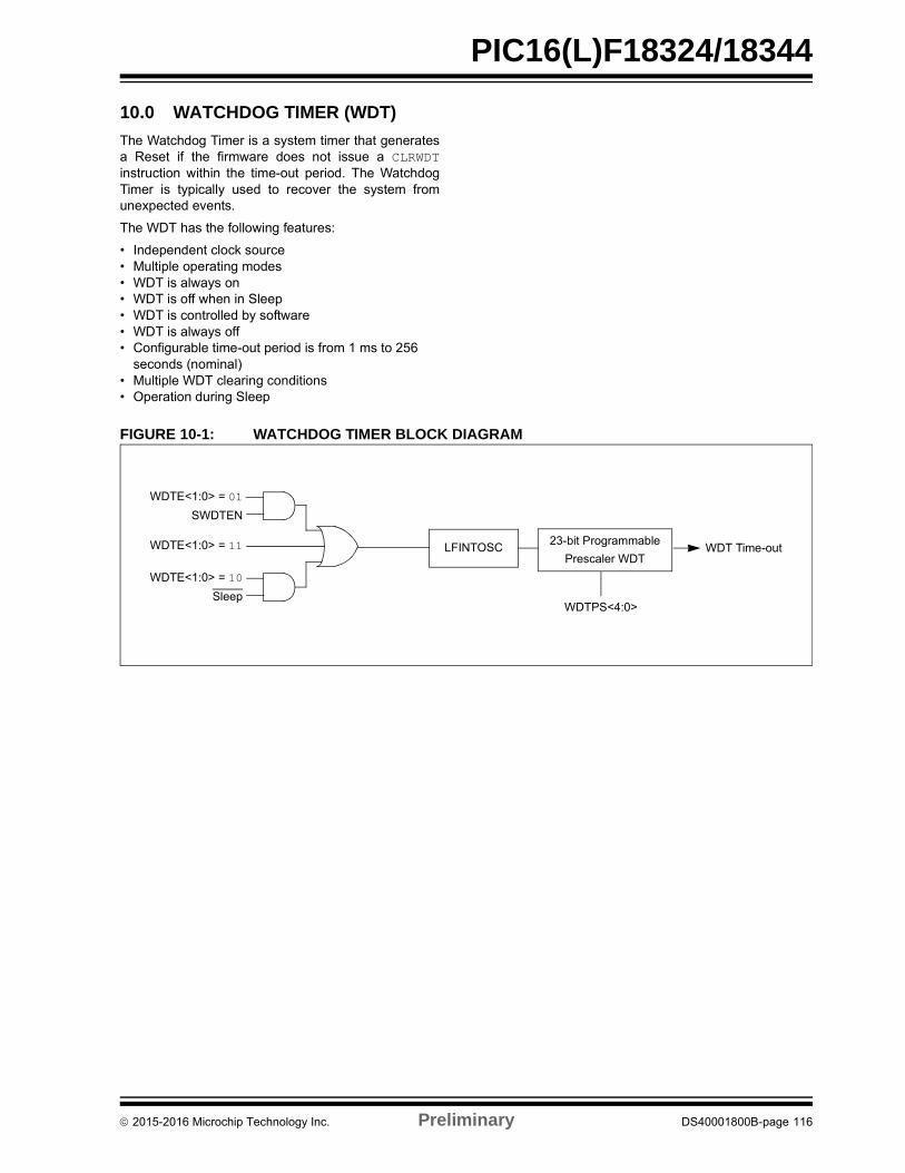
PIC16(L)F18324/18344
10.0 WATCHDOG TIMER (WDT)
The Watchdog Timer is a system timer that generatesa Reset if the firmware does not issue a CLRWDTinstruction within the time-out period. The WatchdogTimer is typically used to recover the system fromunexpected events.
The WDT has the following features:
• Independent clock source• Multiple operating modes• WDT is always on• WDT is off when in Sleep• WDT is controlled by software• WDT is always off• Configurable time-out period is from 1 ms to 256
seconds (nominal)• Multiple WDT clearing conditions• Operation during Sleep
FIGURE 10-1: WATCHDOG TIMER BLOCK DIAGRAM
LFINTOSC23-bit Programmable
Prescaler WDTWDT Time-out
WDTPS<4:0>
SWDTEN
Sleep
WDTE<1:0> = 11
WDTE<1:0> = 01
WDTE<1:0> = 10
2015-2016 Microchip Technology Inc. Preliminary DS40001800B-page 116
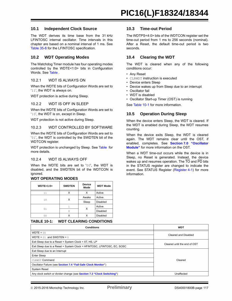
PIC16(L)F18324/18344
10.1 Independent Clock Source
The WDT derives its time base from the 31 kHzLFINTOSC internal oscillator. Time intervals in thischapter are based on a nominal interval of 1 ms. SeeTable 35-8 for the LFINTOSC specification.
10.2 WDT Operating Modes
The Watchdog Timer module has four operating modescontrolled by the WDTE<1:0> bits in ConfigurationWords. See Table .
10.2.1 WDT IS ALWAYS ON
When the WDTE bits of Configuration Words are set to‘11’, the WDT is always on.
WDT protection is active during Sleep.
10.2.2 WDT IS OFF IN SLEEP
When the WDTE bits of Configuration Words are set to‘10’, the WDT is on, except in Sleep.
WDT protection is not active during Sleep.
10.2.3 WDT CONTROLLED BY SOFTWARE
When the WDTE bits of Configuration Words are set to‘01’, the WDT is controlled by the SWDTEN bit of theWDTCON register.
WDT protection is unchanged by Sleep. See Table formore details.
10.2.4 WDT IS ALWAYS OFF
When the WDTE bits are set to '00', the WDT isdisabled, and the SWDTEN bit of the WDTCON isignored.
10.3 Time-out Period
The WDTPS<4:0> bits of the WDTCON register set thetime-out period from 1 ms to 256 seconds (nominal).After a Reset, the default time-out period is twoseconds.
10.4 Clearing the WDT
The WDT is cleared when any of the followingconditions occur:
• Any Reset• CLRWDT instruction is executed• Device enters Sleep• Device wakes up from Sleep due to an interrupt• Oscillator fail• WDT is disabled• Oscillator Start-up Timer (OST) is running
See Table 10-1 for more information.
10.5 Operation During Sleep
When the device enters Sleep, the WDT is cleared. Ifthe WDT is enabled during Sleep, the WDT resumescounting.
When the device exits Sleep, the WDT is clearedagain. The WDT remains clear until the OST, ifenabled, completes. See Section 7.0 “OscillatorModule” for more information on the OST.
When a WDT time-out occurs while the device is inSleep, no Reset is generated. Instead, the devicewakes up and resumes operation. The TO and PD bitsin the STATUS register are changed to indicate theevent. See STATUS Register (Register 4-1) for moreinformation.
WDT OPERATING MODES
WDTE<1:0> SWDTENDevice Mode
WDT Mode
11 X X Active
10 XAwake Active
Sleep Disabled
011
XActive
0 Disabled
00 X X Disabled
TABLE 10-1: WDT CLEARING CONDITIONS
Conditions WDT
WDTE = 00Cleared and Disabled
WDTE = 01 and SWDTEN = 0
Exit Sleep due to a Reset + System Clock = XT, HS, LPCleared until the end of OST
Exit Sleep due to a Reset + System Clock = HFINTOSC, LFINTOSC, EC, SOSC
Exit Sleep due to an Interrupt
Cleared
Enter Sleep
CLRWDT Command
Oscillator Failure (see Section 7.4 “Fail-Safe Clock Monitor”)
System Reset
Any clock switch or divider change (see Section 7.3 “Clock Switching”) Unaffected
2015-2016 Microchip Technology Inc. Preliminary DS40001800B-page 117

PIC16(L)F18324/18344
10.6 Register Definitions: Watchdog Control
REGISTER 10-1: WDTCON: WATCHDOG TIMER CONTROL REGISTER
U-0 U-0 R/W-0/0 R/W-1/1 R/W-0/0 R/W-1/1 R/W-1/1 R/W-0/0
— — WDTPS<4:0>(1) SWDTEN
bit 7 bit 0
Legend:
R = Readable bit W = Writable bit U = Unimplemented bit, read as ‘0’
u = Bit is unchanged x = Bit is unknown -m/n = Value at POR and BOR/Value at all other Resets
‘1’ = Bit is set ‘0’ = Bit is cleared
bit 7-6 Unimplemented: Read as ‘0’
bit 5-1 WDTPS<4:0>: Watchdog Timer Period Select bits(1)
Bit Value = Prescale Rate
11111 = Reserved. Results in minimum interval (1:32) • • •
10011 = Reserved. Results in minimum interval (1:32)
10010 = 1:8388608 (223) (Interval 256s nominal)10001 = 1:4194304 (222) (Interval 128s nominal)10000 = 1:2097152 (221) (Interval 64s nominal)01111 = 1:1048576 (220) (Interval 32s nominal)01110 = 1:524288 (219) (Interval 16s nominal)01101 = 1:262144 (218) (Interval 8s nominal)01100 = 1:131072 (217) (Interval 4s nominal)01011 = 1:65536 (Interval 2s nominal) (Reset value)01010 = 1:32768 (Interval 1s nominal)01001 = 1:16384 (Interval 512 ms nominal)01000 = 1:8192 (Interval 256 ms nominal)00111 = 1:4096 (Interval 128 ms nominal)00110 = 1:2048 (Interval 64 ms nominal)00101 = 1:1024 (Interval 32 ms nominal)00100 = 1:512 (Interval 16 ms nominal)00011 = 1:256 (Interval 8 ms nominal)00010 = 1:128 (Interval 4 ms nominal)00001 = 1:64 (Interval 2 ms nominal)00000 = 1:32 (Interval 1 ms nominal)
bit 0 SWDTEN: Software Enable/Disable for Watchdog Timer bit
If WDTE<1:0> = 1x:This bit is ignored.
If WDTE<1:0> = 01:1 = WDT is turned on0 = WDT is turned off
If WDTE<1:0> = 00:This bit is ignored.
Note 1: Times are approximate. WDT time is based on 31 kHz LFINTOSC.
2015-2016 Microchip Technology Inc. Preliminary DS40001800B-page 118
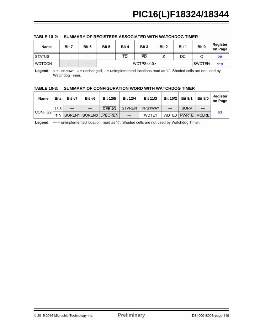
PIC16(L)F18324/18344
TABLE 10-2: SUMMARY OF REGISTERS ASSOCIATED WITH WATCHDOG TIMER
Name Bit 7 Bit 6 Bit 5 Bit 4 Bit 3 Bit 2 Bit 1 Bit 0Register on Page
STATUS — — — TO PD Z DC C 28
WDTCON — — WDTPS<4:0> SWDTEN 118
Legend: x = unknown, u = unchanged, – = unimplemented locations read as ‘0’. Shaded cells are not used by Watchdog Timer.
TABLE 10-3: SUMMARY OF CONFIGURATION WORD WITH WATCHDOG TIMER
Name Bits Bit -/7 Bit -/6 Bit 13/5 Bit 12/4 Bit 11/3 Bit 10/2 Bit 9/1 Bit 8/0Register on Page
CONFIG213:8 — — DEBUG STVREN PPS1WAY — BORV —
637:0 BOREN1 BOREN0 LPBOREN — WDTE1 WDTE0 PWRTE MCLRE
Legend: — = unimplemented location, read as ‘0’. Shaded cells are not used by Watchdog Timer.
2015-2016 Microchip Technology Inc. Preliminary DS40001800B-page 119
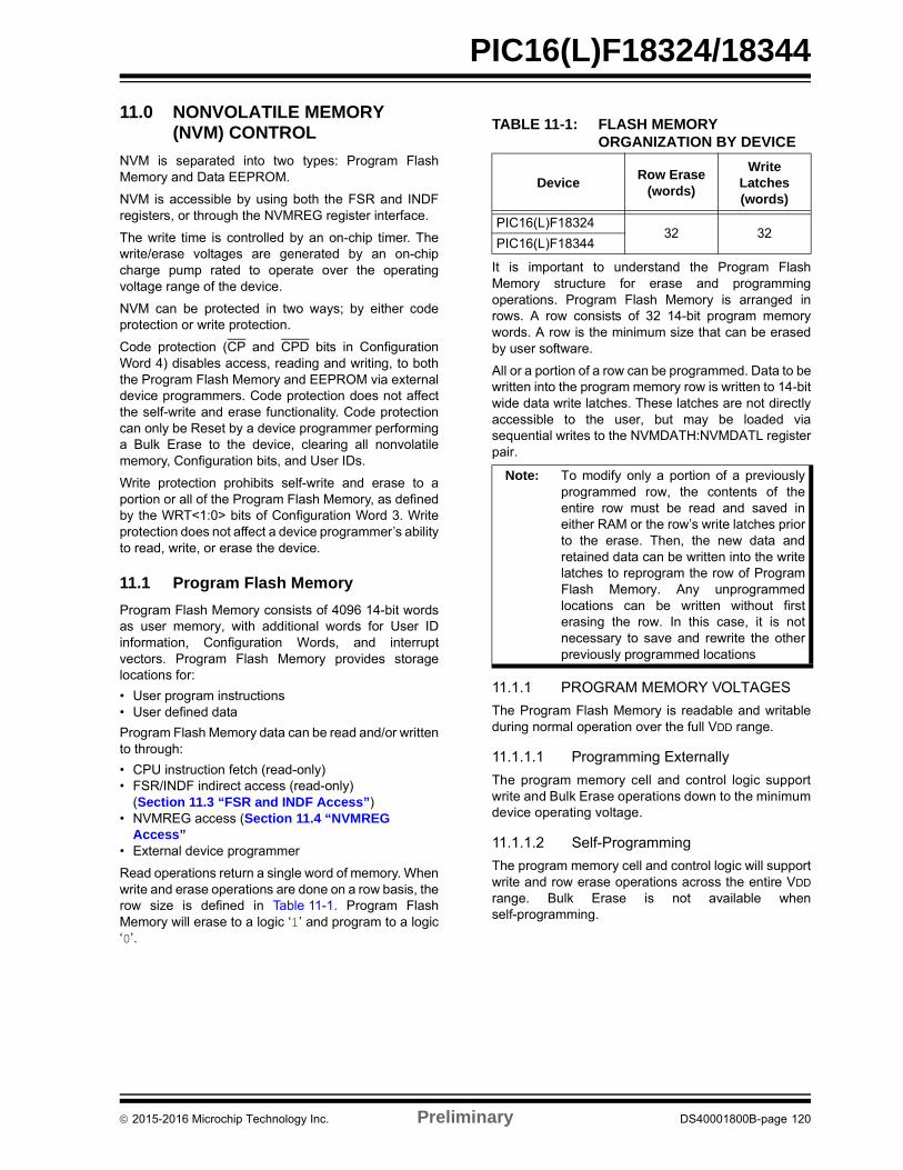
PIC16(L)F18324/18344
11.0 NONVOLATILE MEMORY (NVM) CONTROL
NVM is separated into two types: Program FlashMemory and Data EEPROM.
NVM is accessible by using both the FSR and INDFregisters, or through the NVMREG register interface.
The write time is controlled by an on-chip timer. Thewrite/erase voltages are generated by an on-chipcharge pump rated to operate over the operatingvoltage range of the device.
NVM can be protected in two ways; by either codeprotection or write protection.
Code protection (CP and CPD bits in ConfigurationWord 4) disables access, reading and writing, to boththe Program Flash Memory and EEPROM via externaldevice programmers. Code protection does not affectthe self-write and erase functionality. Code protectioncan only be Reset by a device programmer performinga Bulk Erase to the device, clearing all nonvolatilememory, Configuration bits, and User IDs.
Write protection prohibits self-write and erase to aportion or all of the Program Flash Memory, as definedby the WRT<1:0> bits of Configuration Word 3. Writeprotection does not affect a device programmer’s abilityto read, write, or erase the device.
11.1 Program Flash Memory
Program Flash Memory consists of 4096 14-bit wordsas user memory, with additional words for User IDinformation, Configuration Words, and interruptvectors. Program Flash Memory provides storagelocations for:
• User program instructions• User defined data
Program Flash Memory data can be read and/or writtento through:
• CPU instruction fetch (read-only)• FSR/INDF indirect access (read-only)
(Section 11.3 “FSR and INDF Access”)• NVMREG access (Section 11.4 “NVMREG
Access”• External device programmer
Read operations return a single word of memory. Whenwrite and erase operations are done on a row basis, therow size is defined in Table 11-1. Program FlashMemory will erase to a logic ‘1’ and program to a logic‘0’.
It is important to understand the Program FlashMemory structure for erase and programmingoperations. Program Flash Memory is arranged inrows. A row consists of 32 14-bit program memorywords. A row is the minimum size that can be erasedby user software.
All or a portion of a row can be programmed. Data to bewritten into the program memory row is written to 14-bitwide data write latches. These latches are not directlyaccessible to the user, but may be loaded viasequential writes to the NVMDATH:NVMDATL registerpair.
11.1.1 PROGRAM MEMORY VOLTAGES
The Program Flash Memory is readable and writableduring normal operation over the full VDD range.
11.1.1.1 Programming Externally
The program memory cell and control logic supportwrite and Bulk Erase operations down to the minimumdevice operating voltage.
11.1.1.2 Self-Programming
The program memory cell and control logic will supportwrite and row erase operations across the entire VDD
range. Bulk Erase is not available whenself-programming.
TABLE 11-1: FLASH MEMORY ORGANIZATION BY DEVICE
DeviceRow Erase
(words)
Write Latches (words)
PIC16(L)F1832432 32
PIC16(L)F18344
Note: To modify only a portion of a previouslyprogrammed row, the contents of theentire row must be read and saved ineither RAM or the row’s write latches priorto the erase. Then, the new data andretained data can be written into the writelatches to reprogram the row of ProgramFlash Memory. Any unprogrammedlocations can be written without firsterasing the row. In this case, it is notnecessary to save and rewrite the otherpreviously programmed locations
2015-2016 Microchip Technology Inc. Preliminary DS40001800B-page 120
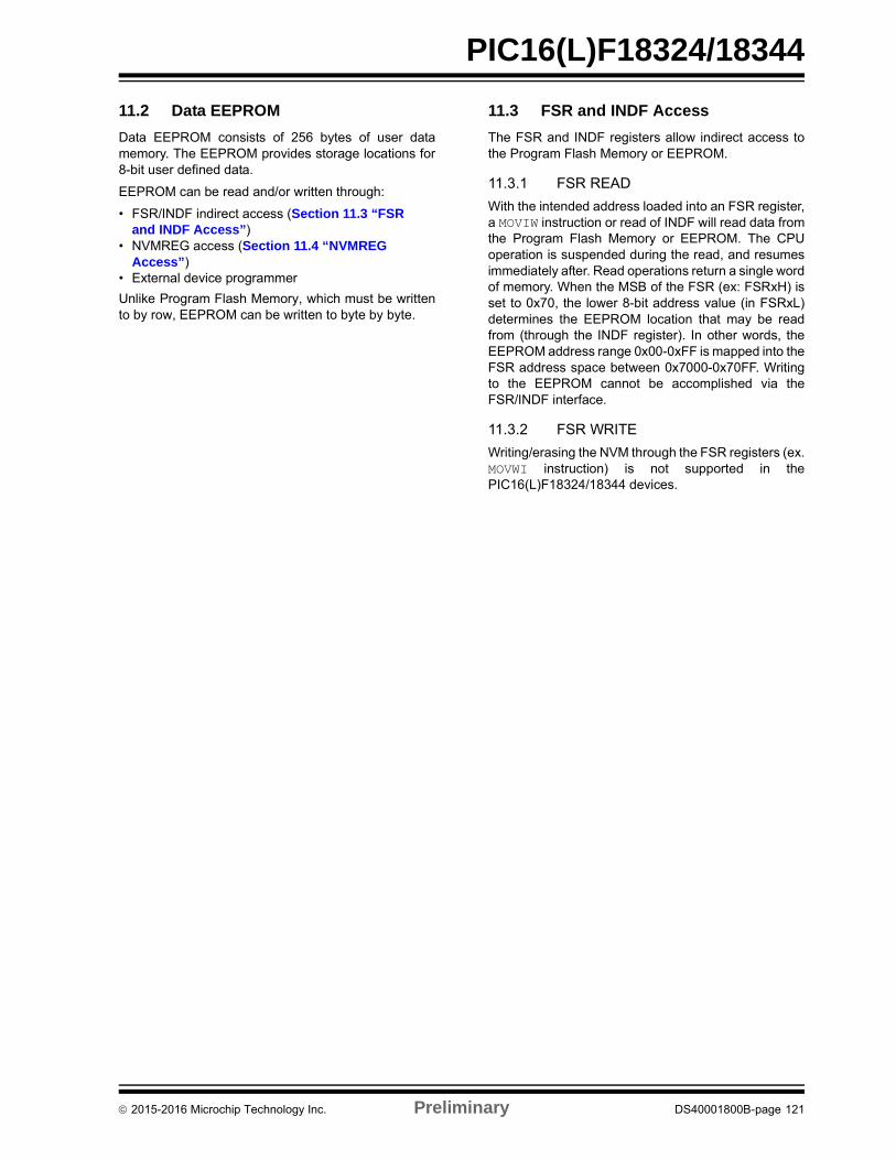
PIC16(L)F18324/18344
11.2 Data EEPROM
Data EEPROM consists of 256 bytes of user datamemory. The EEPROM provides storage locations for8-bit user defined data.
EEPROM can be read and/or written through:
• FSR/INDF indirect access (Section 11.3 “FSR and INDF Access”)
• NVMREG access (Section 11.4 “NVMREG Access”)
• External device programmer
Unlike Program Flash Memory, which must be writtento by row, EEPROM can be written to byte by byte.
11.3 FSR and INDF Access
The FSR and INDF registers allow indirect access tothe Program Flash Memory or EEPROM.
11.3.1 FSR READ
With the intended address loaded into an FSR register,a MOVIW instruction or read of INDF will read data fromthe Program Flash Memory or EEPROM. The CPUoperation is suspended during the read, and resumesimmediately after. Read operations return a single wordof memory. When the MSB of the FSR (ex: FSRxH) isset to 0x70, the lower 8-bit address value (in FSRxL)determines the EEPROM location that may be readfrom (through the INDF register). In other words, theEEPROM address range 0x00-0xFF is mapped into theFSR address space between 0x7000-0x70FF. Writingto the EEPROM cannot be accomplished via theFSR/INDF interface.
11.3.2 FSR WRITE
Writing/erasing the NVM through the FSR registers (ex.MOVWI instruction) is not supported in thePIC16(L)F18324/18344 devices.
2015-2016 Microchip Technology Inc. Preliminary DS40001800B-page 121
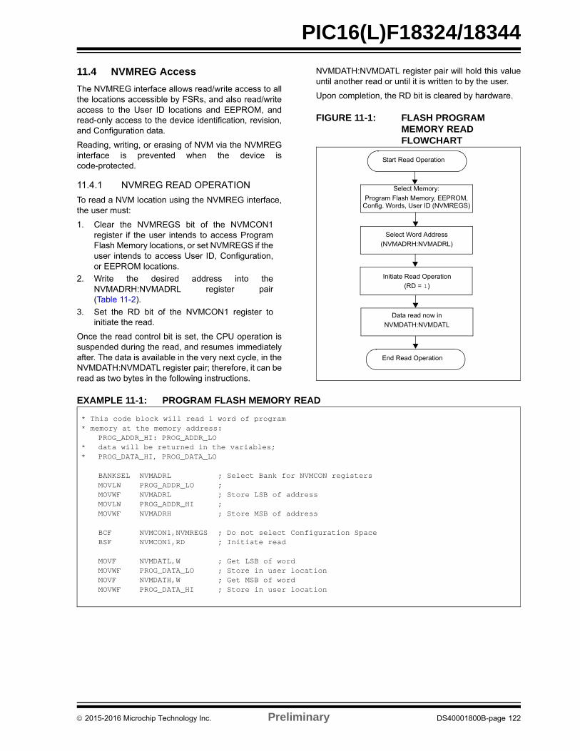
PIC16(L)F18324/18344
11.4 NVMREG Access
The NVMREG interface allows read/write access to allthe locations accessible by FSRs, and also read/writeaccess to the User ID locations and EEPROM, andread-only access to the device identification, revision,and Configuration data.
Reading, writing, or erasing of NVM via the NVMREGinterface is prevented when the device iscode-protected.
11.4.1 NVMREG READ OPERATION
To read a NVM location using the NVMREG interface,the user must:
1. Clear the NVMREGS bit of the NVMCON1register if the user intends to access ProgramFlash Memory locations, or set NVMREGS if theuser intends to access User ID, Configuration,or EEPROM locations.
2. Write the desired address into theNVMADRH:NVMADRL register pair(Table 11-2).
3. Set the RD bit of the NVMCON1 register toinitiate the read.
Once the read control bit is set, the CPU operation issuspended during the read, and resumes immediatelyafter. The data is available in the very next cycle, in theNVMDATH:NVMDATL register pair; therefore, it can beread as two bytes in the following instructions.
NVMDATH:NVMDATL register pair will hold this valueuntil another read or until it is written to by the user.
Upon completion, the RD bit is cleared by hardware.
FIGURE 11-1: FLASH PROGRAM MEMORY READ FLOWCHART
EXAMPLE 11-1: PROGRAM FLASH MEMORY READ
End Read Operation
Select Memory:
Program Flash Memory, EEPROM, Config. Words, User ID (NVMREGS)
Select Word Address
(NVMADRH:NVMADRL)
Start Read Operation
Initiate Read Operation
(RD = 1)
Data read now in
NVMDATH:NVMDATL
* This code block will read 1 word of program* memory at the memory address:
PROG_ADDR_HI: PROG_ADDR_LO* data will be returned in the variables;* PROG_DATA_HI, PROG_DATA_LO
BANKSEL NVMADRL ; Select Bank for NVMCON registersMOVLW PROG_ADDR_LO ; MOVWF NVMADRL ; Store LSB of addressMOVLW PROG_ADDR_HI ; MOVWF NVMADRH ; Store MSB of address
BCF NVMCON1,NVMREGS ; Do not select Configuration SpaceBSF NVMCON1,RD ; Initiate read
MOVF NVMDATL,W ; Get LSB of wordMOVWF PROG_DATA_LO ; Store in user locationMOVF NVMDATH,W ; Get MSB of wordMOVWF PROG_DATA_HI ; Store in user location
2015-2016 Microchip Technology Inc. Preliminary DS40001800B-page 122
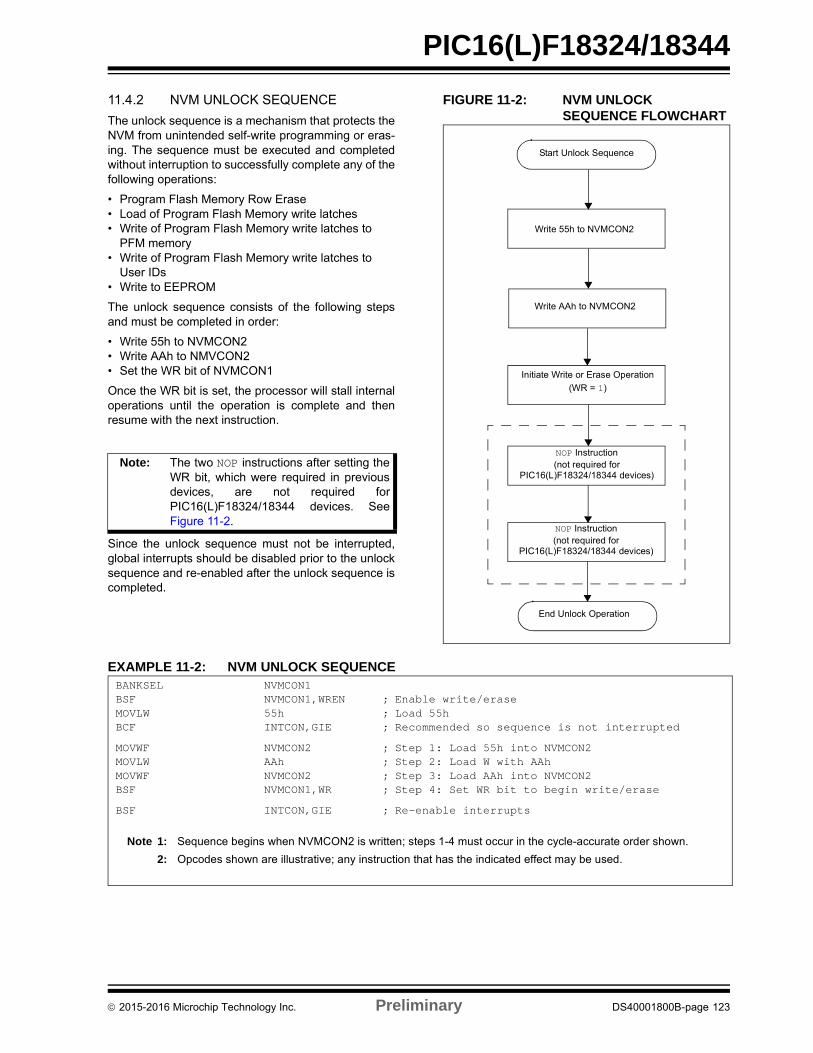
PIC16(L)F18324/18344
11.4.2 NVM UNLOCK SEQUENCE
The unlock sequence is a mechanism that protects theNVM from unintended self-write programming or eras-ing. The sequence must be executed and completedwithout interruption to successfully complete any of thefollowing operations:
• Program Flash Memory Row Erase• Load of Program Flash Memory write latches• Write of Program Flash Memory write latches to
PFM memory• Write of Program Flash Memory write latches to
User IDs• Write to EEPROM
The unlock sequence consists of the following stepsand must be completed in order:
• Write 55h to NVMCON2• Write AAh to NMVCON2• Set the WR bit of NVMCON1
Once the WR bit is set, the processor will stall internaloperations until the operation is complete and thenresume with the next instruction.
Since the unlock sequence must not be interrupted,global interrupts should be disabled prior to the unlocksequence and re-enabled after the unlock sequence iscompleted.
FIGURE 11-2: NVM UNLOCK SEQUENCE FLOWCHART
EXAMPLE 11-2: NVM UNLOCK SEQUENCE
Note: The two NOP instructions after setting theWR bit, which were required in previousdevices, are not required forPIC16(L)F18324/18344 devices. SeeFigure 11-2.
End Unlock Operation
Write 55h to NVMCON2
Write AAh to NVMCON2
Initiate Write or Erase Operation
(WR = 1)
NOP Instruction(not required for
PIC16(L)F18324/18344 devices)
NOP Instruction(not required for
PIC16(L)F18324/18344 devices)
Start Unlock Sequence
Note 1: Sequence begins when NVMCON2 is written; steps 1-4 must occur in the cycle-accurate order shown.
2: Opcodes shown are illustrative; any instruction that has the indicated effect may be used.
BANKSEL NVMCON1BSF NVMCON1,WREN ; Enable write/eraseMOVLW 55h ; Load 55hBCF INTCON,GIE ; Recommended so sequence is not interrupted
MOVWF NVMCON2 ; Step 1: Load 55h into NVMCON2MOVLW AAh ; Step 2: Load W with AAhMOVWF NVMCON2 ; Step 3: Load AAh into NVMCON2BSF NVMCON1,WR ; Step 4: Set WR bit to begin write/erase
BSF INTCON,GIE ; Re-enable interrupts
2015-2016 Microchip Technology Inc. Preliminary DS40001800B-page 123
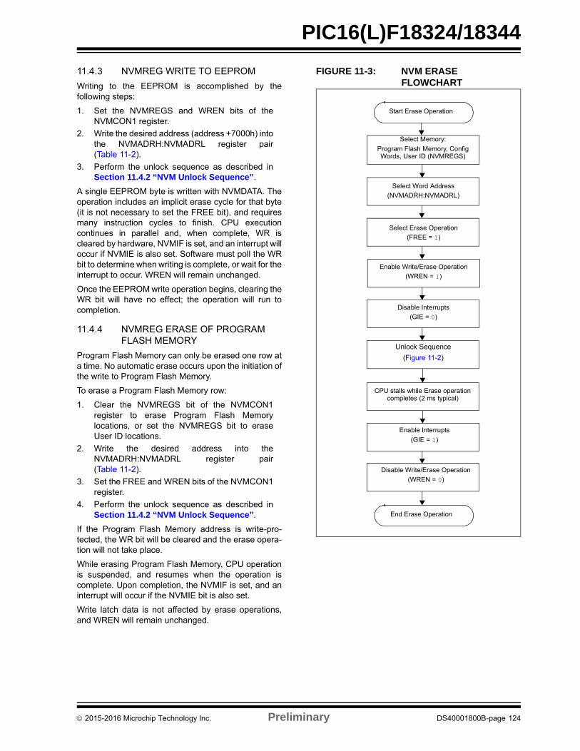
PIC16(L)F18324/18344
11.4.3 NVMREG WRITE TO EEPROM
Writing to the EEPROM is accomplished by thefollowing steps:
1. Set the NVMREGS and WREN bits of theNVMCON1 register.
2. Write the desired address (address +7000h) intothe NVMADRH:NVMADRL register pair(Table 11-2).
3. Perform the unlock sequence as described inSection 11.4.2 “NVM Unlock Sequence”.
A single EEPROM byte is written with NVMDATA. Theoperation includes an implicit erase cycle for that byte(it is not necessary to set the FREE bit), and requiresmany instruction cycles to finish. CPU executioncontinues in parallel and, when complete, WR iscleared by hardware, NVMIF is set, and an interrupt willoccur if NVMIE is also set. Software must poll the WRbit to determine when writing is complete, or wait for theinterrupt to occur. WREN will remain unchanged.
Once the EEPROM write operation begins, clearing theWR bit will have no effect; the operation will run tocompletion.
11.4.4 NVMREG ERASE OF PROGRAM FLASH MEMORY
Program Flash Memory can only be erased one row ata time. No automatic erase occurs upon the initiation ofthe write to Program Flash Memory.
To erase a Program Flash Memory row:
1. Clear the NVMREGS bit of the NVMCON1register to erase Program Flash Memorylocations, or set the NVMREGS bit to eraseUser ID locations.
2. Write the desired address into theNVMADRH:NVMADRL register pair(Table 11-2).
3. Set the FREE and WREN bits of the NVMCON1register.
4. Perform the unlock sequence as described inSection 11.4.2 “NVM Unlock Sequence”.
If the Program Flash Memory address is write-pro-tected, the WR bit will be cleared and the erase opera-tion will not take place.
While erasing Program Flash Memory, CPU operationis suspended, and resumes when the operation iscomplete. Upon completion, the NVMIF is set, and aninterrupt will occur if the NVMIE bit is also set.
Write latch data is not affected by erase operations,and WREN will remain unchanged.
FIGURE 11-3: NVM ERASE FLOWCHART
Unlock Sequence
(Figure 11-2)
End Erase Operation
Select Memory:
Program Flash Memory, Config Words, User ID (NVMREGS)
Disable Write/Erase Operation
(WREN = 0)
Select Word Address
(NVMADRH:NVMADRL)
Start Erase Operation
CPU stalls while Erase operation completes (2 ms typical)
Select Erase Operation
(FREE = 1)
Disable Interrupts
(GIE = 0)
Enable Interrupts
(GIE = 1)
Enable Write/Erase Operation
(WREN = 1)
2015-2016 Microchip Technology Inc. Preliminary DS40001800B-page 124
PIC16(L)F18324/18344
EXAMPLE 11-3: ERASING ONE ROW OF PROGRAM FLASH MEMORY
; This sample row erase routine assumes the following:; 1.A valid address within the erase row is loaded in variables ADDRH:ADDRL; 2.ADDRH and ADDRL are located in common RAM (locations 0x70 - 0x7F)
BANKSEL NVMADRLMOVF ADDRL,WMOVWF NVMADRL ; Load lower 8 bits of erase address boundaryMOVF ADDRH,WMOVWF NVMADRH ; Load upper 6 bits of erase address boundaryBCF NVMCON1,NVMREGS ; Choose Program Flash Memory memory areaBSF NVMCON1,FREE ; Specify an erase operationBSF NVMCON1,WREN ; Enable writesBCF INTCON,GIE ; Disable interrupts during unlock sequence
; -------------------------------REQUIRED UNLOCK SEQUENCE:------------------------------
MOVLW 55h ; Load 55h to get ready for unlock sequenceMOVWF NVMCON2 ; First step is to load 55h into NVMCON2MOVLW AAh ; Second step is to load AAh into WMOVWF NVMCON2 ; Third step is to load AAh into NVMCON2BSF NVMCON1,WR ; Final step is to set WR bit
; --------------------------------------------------------------------------------------
BSF INTCON,GIE ; Re-enable interrupts, erase is completeBCF NVMCON1,WREN ; Disable writes
TABLE 11-2: NVM ORGANIZATION AND ACCESS INFORMATION
Master Values NVMREG Access FSR Access
MemoryFunction
Program Counter (PC), ICSP Address
Memory Type
NVMREGS bit
(NVMCON1)
NVMADR<14:0>
Allowed Operations
FSRAddress
FSRProgramming
Address
Reset Vector 0000h
Program Flash
Memory
0 0000h
READWRITE
8000h
READ-ONLY
User Memory 0001h 0 0001h 8001h
0003h 0003h 8003h
INT Vector 0004h 0 0004h 8004h
User Memory 0005h 0 0005h 8005h
FFFh FFFh FFFFh
User ID
No PC Address
Program Flash
Memory
1 0000hREAD
No Access
0003h
Reserved — — 0004h —
Rev ID
Program Flash
Memory
1 0005h
READ
Device ID 1 0006h
CONFIG1 1 0007h
CONFIG2 1 0008h
CONFIG3 1 0009h
CONFIG4 000Ah
User Memory EEPROM 1 7000h READ 7000h READ-ONLY
70FFh WRITE 70FFh
2015-2016 Microchip Technology Inc. Preliminary DS40001800B-page 125
PIC16(L)F18324/18344
11.4.5 NVMREG WRITE TO PROGRAM FLASH MEMORY
Program memory is programmed using the followingsteps:
1. Load the address of the row to be programmedinto NVMADRH:NVMADRL.
2. Load each write latch with data.
3. Initiate a programming operation.
4. Repeat steps 1 through 3 until all data is written.
Before writing to program memory, the word(s) to bewritten must be erased or previously unwritten.Program memory can only be erased one row at a time.No automatic erase occurs upon the initiation of thewrite.
Program memory can be written one or more words ata time. The maximum number of words written at onetime is equal to the number of write latches. SeeFigure 11-4 (row writes to program memory with 32write latches) for more details.
The write latches are aligned to the Flash row addressboundary defined by the upper ten bits ofNVMADRH:NVMADRL, (NVMADRH<6:0>:NVMADRL<7:5>)with the lower five bits of NVMADRL, (NVMADRL<4:0>)determining the write latch being loaded. Write opera-tions do not cross these boundaries. At the completionof a program memory write operation, the data in thewrite latches is reset to contain 0x3FFF.
The following steps should be completed to load thewrite latches and program a row of program memory.These steps are divided into two parts. First, each writelatch is loaded with data from theNVMDATH:NVMDATL using the unlock sequence withLWLO = 1. When the last word to be loaded into thewrite latch is ready, the LWLO bit is cleared and theunlock sequence executed. This initiates theprogramming operation, writing all the latches intoFlash program memory.
1. Set the WREN bit of the NVMCON1 register.
2. Clear the NVMREGS bit of the NVMCON1register.
3. Set the LWLO bit of the NVMCON1 register.When the LWLO bit of the NVMCON1 register is‘1’, the write sequence will only load the writelatches and will not initiate the write to Flashprogram memory.
4. Load the NVMADRH:NVMADRL register pairwith the address of the location to be written.
5. Load the NVMDATH:NVMDATL register pairwith the program memory data to be written.
6. Execute the unlock sequence (Section 11.4.2“NVM Unlock Sequence”). The write latch isnow loaded.
7. Increment the NVMADRH:NVMADRL registerpair to point to the next location.
8. Repeat steps 5 through 7 until all but the lastwrite latch has been loaded.
9. Clear the LWLO bit of the NVMCON1 register.When the LWLO bit of the NVMCON1 register is‘0’, the write sequence will initiate the write toFlash program memory.
10. Load the NVMDATH:NVMDATL register pairwith the program memory data to be written.
11. Execute the unlock sequence (Section 11.4.2“NVM Unlock Sequence”). The entire programmemory latch content is now written to Flashprogram memory.
An example of the complete write sequence is shown inExample 11-4. The initial address is loaded into theNVMADRH:NVMADRL register pair; the data is loadedusing indirect addressing.
Note: The special unlock sequence is requiredto load a write latch with data or initiate aFlash programming operation. If theunlock sequence is interrupted, writing tothe latches or program memory will not beinitiated.
Note: The program memory write latches arereset to the blank state (0x3FFF) at thecompletion of every write or eraseoperation. As a result, it is not necessaryto load all the program memory writelatches. Unloaded latches will remain inthe blank state.
2015-2016 Microchip Technology Inc. Preliminary DS40001800B-page 126
2
01
5-2
01
6 M
icroch
ip T
ech
no
log
y Inc.
Prelim
inary
DS
40
00
18
00
B-p
ag
e 1
27
PIC
16(L)F
18324/18344
FIG
8
Write Latch #311Fh
1414
14
ory
Write Latch #301Eh
Addr Addr
001Fh001Eh
003Fh003Eh
005Fh005Eh
7FDFh7FDEh
7FFFh7FFEh
14
800Bh - 801Fh
rationrds
800Ah
reserved
mory
MDATL 0
URE 11-4: BLOCK WRITES TO PROGRAM FLASH MEMORY WITH 32 WRITE LATCHES
6
14
1414
Program Memory Write Latches
14 14
NVMADRH<6:0>NVMADRL<7:5>
Program Flash Mem
Row
Row Address Decode
Addr
Write Latch #101h
Write Latch #000h
Addr
000h 0000h 0001h
001h 0020h 0021h
002h 0040h 0041h
3FEh 7FC0h 7FC1h
3FFh 7FE0h 7FE1h
NVMADRL<4:0>
400h 8000h - 8003h
ConfiguWo
USER ID 0 - 3
8007h –8005h -8006h
DEVICE IDDev / Rev
reserved
Configuration Me
NVMREGS = 0
NVMREGS = 1
NVMADRH NVMADRL7 6 0 7 5 4 0
c4 c3 c2 c1 c0r9 r8 r7 r6 r5 r4 r3- r1 r0r2
510
NVMDATH NV7 5 0 7
--
8004h
PIC16(L)F18324/18344
FIGURE 11-5: PROGRAM FLASH MEMORY WRITE FLOWCHART
Start Write Operation
Determine number of words to be written into
Program Flash Memory or Configuration Memory. The number of words
cannot exceed the number of words per row
(word_cnt)
Select Program Flash Memory or
Config. Memory (NVMREGS)
Select Row Address(NVMADRH:NVMADRL)
Select Write Operation(FREE = 0)
Load Write Latches Only(LWLO = 1)
Disable Interrupts(GIE = 0)
Enable Write/EraseOperation (WREN = 1)
Load the value to write(NVMDATH:NVMDATL)
Update the word counter(word_cnt--)
Last word to write?
Unlock Sequence
No delay when writing to Program Flash Memory
Latches
Re-enable Interrupts(GIE = 1)
Write Latches to PFM(LWLO = 0)
Disable Interrupts(GIE = 0)
CPU stalls while Write operation completes
(2 ms typical)
Disable Write/Erase Operation (WREN = 0)
End Write Operation
Increment Address(NVMADRH:NVMADRL++)
Unlock Sequence
Re-enable Interrupts(GIE = 1)
Yes
No
(Figure 11-2)
(Figure 11-2)
2015-2016 Microchip Technology Inc. Preliminary DS40001800B-page 128
PIC16(L)F18324/18344
EXAMPLE 11-4: WRITING TO PROGRAM FLASH MEMORY ; This write routine assumes the following:; 1. 32 words of data are loaded, starting at the address in DATA_ADDR; 2. Each word of data to be written is made up of two adjacent bytes in DATA_ADDR,; stored in little endian format; 3. A valid starting address (the least significant bits = 00000) is loaded in ADDRH:ADDRL; 4. ADDRH and ADDRL are located in common RAM (locations 0x70 - 0x7F); 5. NVM interrupts are not taken into account
BANKSEL NVMADRHMOVF ADDRH,WMOVWF NVMADRH ; Load initial addressMOVF ADDRL,WMOVWF NVMADRLMOVLW LOW DATA_ADDR ; Load initial data addressMOVWF FSR0LMOVLW HIGH DATA_ADDRMOVWF FSR0HBCF NVMCON1,NVMREGS ; Set Program Flash Memory as write locationBSF NVMCON1,WREN ; Enable writesBSF NVMCON1,LWLO ; Load only write latches
LOOPMOVIW FSR0++MOVWF NVMDATL ; Load first data byteMOVIW FSR0++MOVWF NVMDATH ; Load second data byte
MOVF NVMADRL,WXORLW 0x1F ; Check if lower bits of address are 00000ANDLW 0x1F ; and if on last of 32 addressesBTFSC STATUS,Z ; Last of 32 words?GOTO START_WRITE ; If so, go write latches into memory
CALL UNLOCK_SEQ ; If not, go load latchINCF NVMADRL,F ; Increment addressGOTO LOOP
START_WRITEBCF NVMCON1,LWLO ; Latch writes complete, now write memoryCALL UNLOCK_SEQ ; Perform required unlock sequenceBCF NVMCON1,LWLO ; Disable writes
UNLOCK_SEQMOVLW 55hBCF INTCON,GIE ; Disable interruptsMOVWF NVMCON2 ; Begin unlock sequenceMOVLW AAhMOVWF NVMCON2BSF NVMCON1,WRBSF INTCON,GIE ; Unlock sequence complete, re-enable interruptsreturn
2015-2016 Microchip Technology Inc. Preliminary DS40001800B-page 129
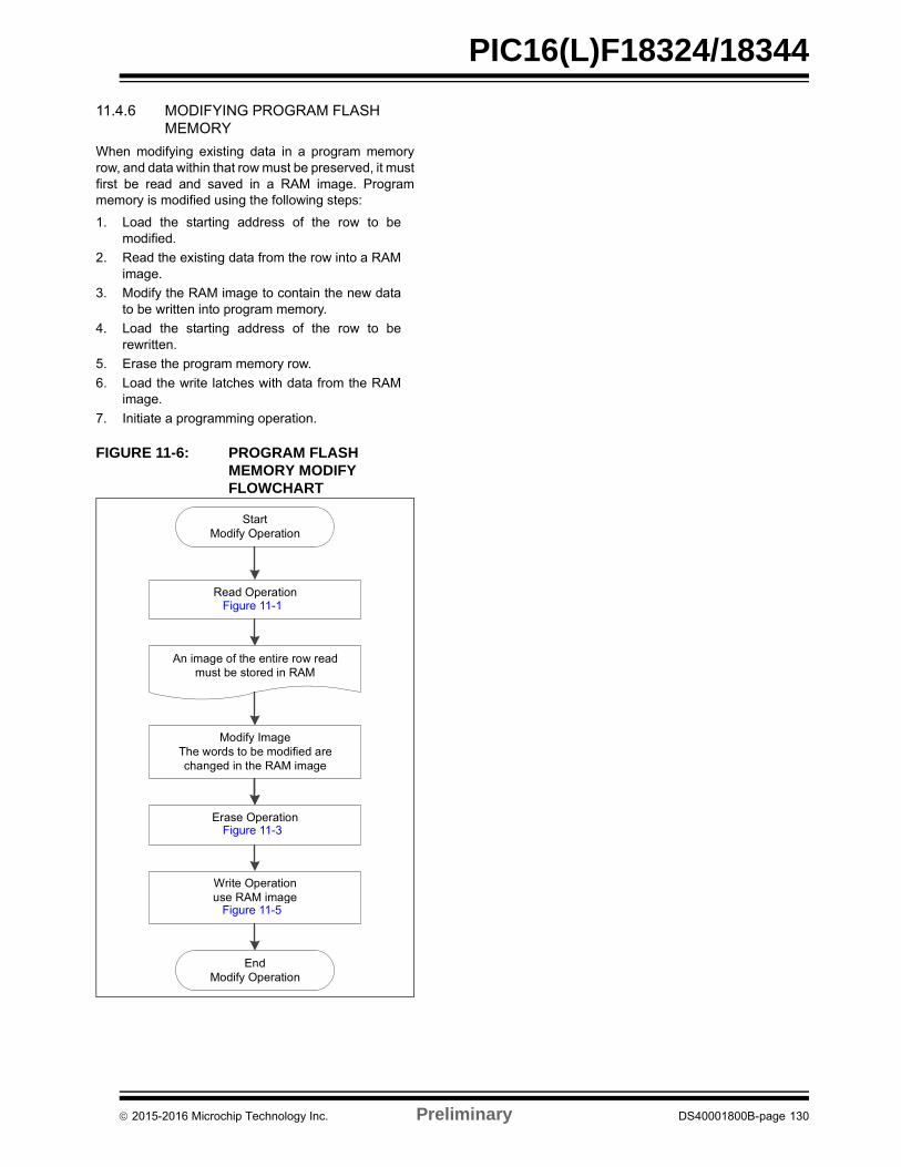
PIC16(L)F18324/18344
11.4.6 MODIFYING PROGRAM FLASH MEMORY
When modifying existing data in a program memoryrow, and data within that row must be preserved, it mustfirst be read and saved in a RAM image. Programmemory is modified using the following steps:
1. Load the starting address of the row to bemodified.
2. Read the existing data from the row into a RAMimage.
3. Modify the RAM image to contain the new datato be written into program memory.
4. Load the starting address of the row to berewritten.
5. Erase the program memory row.
6. Load the write latches with data from the RAMimage.
7. Initiate a programming operation.
FIGURE 11-6: PROGRAM FLASH MEMORY MODIFY FLOWCHART
Start Modify Operation
Read Operation(Figure x.x)
Erase Operation(Figure x.x)
Modify ImageThe words to be modified are changed in the RAM image
End Modify Operation
Write Operationuse RAM image
(Figure x.x)
An image of the entire row read must be stored in RAM
Figure 11-1
Figure 11-3
Figure 11-5
2015-2016 Microchip Technology Inc. Preliminary DS40001800B-page 130
PIC16(L)F18324/18344
11.4.7 NVMREG EEPROM, USER ID, DEVICE ID AND CONFIGURATION WORD ACCESS
Instead of accessing Program Flash Memory, theEEPROM, the User ID’s, Device ID/Revision ID andConfiguration Words can be accessed whenNVMREGS = 1 in the NVMCON1 register. This is theregion that would be pointed to by PC<15> = 1, but notall addresses are accessible. Different access mayexist for reads and writes. Refer to Table 11-3.
When read access is initiated on an address outsidethe parameters listed in Table 11-3, the NVMDATH:NVMDATL register pair is cleared, reading back ‘0’s.
TABLE 11-3: EEPROM, USER ID, DEV/REV ID AND CONFIGURATION WORD ACCESS (NVMREGS = 1)
Address Function Read Access Write Access
8000h-8003h User IDs Yes Yes
8005h-8006h Device ID/Revision ID Yes No
8007h-800Ah Configuration Words 1-4 Yes No
F000h-F0FFh EEPROM Yes Yes
2015-2016 Microchip Technology Inc. Preliminary DS40001800B-page 131
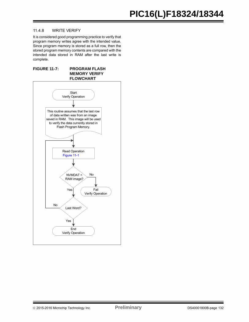
PIC16(L)F18324/18344
11.4.8 WRITE VERIFY
It is considered good programming practice to verify thatprogram memory writes agree with the intended value.Since program memory is stored as a full row, then thestored program memory contents are compared with theintended data stored in RAM after the last write iscomplete.
FIGURE 11-7: PROGRAM FLASH MEMORY VERIFY FLOWCHART
Start Verify Operation
Read Operation
End Verify Operation
This routine assumes that the last row of data written was from an image
saved in RAM. This image will be used to verify the data currently stored in
Flash Program Memory.
NVMDAT = RAM image?
Last Word?
Fail Verify Operation
No
Yes
Yes
No
Figure 11-1
2015-2016 Microchip Technology Inc. Preliminary DS40001800B-page 132
PIC16(L)F18324/18344
11.4.9 WRERR BIT
The WRERR bit can be used to determine if a writeerror occurred.
WRERR will be set if one of the following conditionsoccurs:
• If WR is set while the NVMADRH:NMVADRL points to a write-protected address
• A Reset occurs while a self-write operation was in progress
• An unlock sequence was interrupted
The WRERR bit is normally set by hardware, but canbe set by the user for test purposes. Once set, WRERRmust be cleared in software.
TABLE 11-4: ACTIONS FOR PROGRAM FLASH MEMORY WHEN WR = 1
Free LWLO Actions for Program Flash Memory when WR = 1 Comments
0 0 Write the write-latch data to Program Flash Memory row. See Section 11.4.4 “NVMREG Erase of Pro-gram Flash Memory”
• If WP is enabled, WR is cleared and WRERR is set
• Write latches are reset to 3FFh• NVMDATH:NVMDATL is ignored
0 1 Copy NVMDATH:NVMDATL to the write latch corre-sponding to NVMADR LSBs. See Section 11.4.4 “NVMREG Erase of Program Flash Memory”
• Write protection is ignored• No memory access occurs
1 x Erase the 32-word row of NVMADRH:NVMADRL location. See Section 11.4.3 “NVMREG Write to EEPROM”
• If WP is enabled, WR is cleared and WRERR is set
• All 32 words are erased• NVMDATH:NVMDATL is ignored
2015-2016 Microchip Technology Inc. Preliminary DS40001800B-page 133
PIC16(L)F18324/18344
11.5 Register Definitions: Flash Program Memory Control
REGISTER 11-1: NVMDATL: NONVOLATILE MEMORY DATA LOW BYTE REGISTERR/W-0/0 R/W-0/0 R/W-0/0 R/W-0/0 R/W-0/0 R/W-0/0 R/W-0/0 R/W-0/0
NVMDAT<7:0>
bit 7 bit 0
Legend:
R = Readable bit W = Writable bit U = Unimplemented bit, read as ‘0’
u = Bit is unchanged x = Bit is unknown -n/n = Value at POR and BOR/Value at all other Resets
‘1’ = Bit is set ‘0’ = Bit is cleared
bit 7-0 NVMDAT<7:0>: Read/write value for Least Significant bits of program memory
REGISTER 11-2: NVMDATH: NONVOLATILE MEMORY DATA HIGH BYTE REGISTERU-0 U-0 R/W-0/0 R/W-0/0 R/W-0/0 R/W-0/0 R/W-0/0 R/W-0/0
— — NVMDAT<13:8>
bit 7 bit 0
Legend:
R = Readable bit W = Writable bit U = Unimplemented bit, read as ‘0’
u = Bit is unchanged x = Bit is unknown -n/n = Value at POR and BOR/Value at all other Resets
‘1’ = Bit is set ‘0’ = Bit is cleared
bit 7-6 Unimplemented: Read as ‘0’
bit 5-0 NVMDAT<13:8>: Read/write value for Most Significant bits of program memory(1)
Note 1: This byte is ignored when writing to EEPROM.
REGISTER 11-3: NVMADRL: NONVOLATILE MEMORY ADDRESS LOW BYTE REGISTERR/W-0/0 R/W-0/0 R/W-0/0 R/W-0/0 R/W-0/0 R/W-0/0 R/W-0/0 R/W-0/0
NVMADR<7:0>
bit 7 bit 0
Legend:
R = Readable bit W = Writable bit U = Unimplemented bit, read as ‘0’
u = Bit is unchanged x = Bit is unknown -n/n = Value at POR and BOR/Value at all other Resets
‘1’ = Bit is set ‘0’ = Bit is cleared
bit 7-0 NVMADR<7:0>: Specifies the Least Significant bits for program memory address
REGISTER 11-4: NVMADRH: NONVOLATILE MEMORY ADDRESS HIGH BYTE REGISTERU-1 R/W-0/0 R/W-0/0 R/W-0/0 R/W-0/0 R/W-0/0 R/W-0/0 R/W-0/0
— NVMADR<14:8>
bit 7 bit 0
Legend:
R = Readable bit W = Writable bit U = Unimplemented bit, read as ‘0’
u = Bit is unchanged x = Bit is unknown -n/n = Value at POR and BOR/Value at all other Resets
‘1’ = Bit is set ‘0’ = Bit is cleared
bit 7 Unimplemented: Read as ‘1’
bit 6-0 NVMADR<14:8>: Specifies the Most Significant bits for program memory address
2015-2016 Microchip Technology Inc. Preliminary DS40001800B-page 134
PIC16(L)F18324/18344
REGISTER 11-5: NVMCON1: NONVOLATILE MEMORY CONTROL 1 REGISTER
U-0 R/W-0/0 R/W-0/0 R/W/HC-0/0 R/W/HC-x/q R/W-0/0 R/S/HC-0/0 R/S/HC-0/0
— NVMREGS LWLO FREE WRERR WREN WR RD
bit 7 bit 0
Legend:
R = Readable bit W = Writable bit U = Unimplemented bit, read as ‘0’
S = Bit can only be set x = Bit is unknown -n/n = Value at POR and BOR/Value at all other Resets
‘1’ = Bit is set ‘0’ = Bit is cleared HC = Bit is cleared by hardware
bit 7 Unimplemented: Read as ‘0’
bit 6 NVMREGS: Configuration Select bit1 = Access EEPROM, Configuration, User ID and Device ID registers0 = Access Program Flash Memory
bit 5 LWLO: Load Write Latches Only bitWhen FREE = 0:1 = The next WR command updates the write latch for this word within the row; no memory operation
is initiated.0 = The next WR command writes data or erases.Otherwise: The bit is ignored.
bit 4 FREE: Program Flash Memory Erase Enable bit When NVMREGS:NVMADR points to a Program Flash Memory location:1 = Performs an erase operation with the next WR command; the row containing the indicated address
is erased (to all 1s) to prepare for writing.0 = All erase operations have completed normally.
bit 3 WRERR: Program/Erase Error Flag bit (1,2,3)
This bit is normally set by hardware.1 = A write operation was interrupted by a Reset, interrupted unlock sequence, or WR was written to
one while NVMADR points to a write-protected address.0 = The program or erase operation completed normally
bit 2 WREN: Program/Erase Enable bit1 = Allows program/erase cycles0 = Inhibits programming/erasing of program Flash
bit 1 WR: Write Control bit(4,5,6)
When NVMREG:NVMADR points to a EEPROM location:1 = Initiates an erase/program cycle at the corresponding EEPROM location0 = NVM program/erase operation is complete and inactiveWhen NVMREG:NVMADR points to a Program Flash Memory location:1 = Initiates the operation indicated by Table 11-50 = NVM program/erase operation is complete and inactive
bit 0 RD: Read Control bit(7)
1 = Initiates a read at address = NVMADR1, and loads data to NVMDAT Read takes one instructioncycle and the bit is cleared when the operation is complete. The bit can only be set (not cleared)in software.
0 = NVM read operation is complete and inactive.
Note 1: Bit may change while WR = 1 (during the EEPROM write operation it may be ‘0’ or ‘1’).2: Bit must be cleared by software; hardware will not clear this bit.3: Bit may be written to ‘1’ by software in order to implement test sequences.4: This bit can only be set by following the unlock sequence of Section 11.4.2 “NVM Unlock Sequence”.5: Operations are self-timed, and the WR bit is cleared by hardware when complete.6: Once a write operation is initiated, setting this bit to zero will have no effect.7: Reading from EEPROM loads only NVMDATL<7:0> (Register 11-1).
2015-2016 Microchip Technology Inc. Preliminary DS40001800B-page 135
PIC16(L)F18324/18344
REGISTER 11-6: NVMCON2: NONVOLATILE MEMORY CONTROL 2 REGISTER
W-0/0 W-0/0 W-0/0 W-0/0 W-0/0 W-0/0 W-0/0 W-0/0
NVMCON2
bit 7 bit 0
Legend:
R = Readable bit W = Writable bit U = Unimplemented bit, read as ‘0’
S = Bit can only be set x = Bit is unknown -n/n = Value at POR and BOR/Value at all other Resets
‘1’ = Bit is set ‘0’ = Bit is cleared
bit 7-0 NVMCON2<7:0>: Flash Memory Unlock Pattern bits
To unlock writes, a 55h must be written first, followed by an AAh, before setting the WR bit of theNVMCON1 register. The value written to this register is used to unlock the writes.
TABLE 11-5: SUMMARY OF REGISTERS ASSOCIATED WITH NONVOLATILE MEMORY (NVM)
Name Bit 7 Bit 6 Bit 5 Bit 4 Bit 3 Bit 2 Bit 1 Bit 0Register on Page
INTCON GIE PEIE — — — — — INTEDG 98
PIR2 TMR6IF C2IF C1IF NVMIF ― ― TMR4IF NCO1IF 106
PIE2 TMR6IE C2IE C1IE NVMIE ― ― TMR4IE NCO1IE 101
NVMCON1 — NVMREGS LWLO FREE WRERR WREN WR RD 135
NVMCON2 NVMCON2 136
NVMADRL NVMADR<7:0> 134
NVMADRH —(1) NVMADR<14:8> 134
NVMDATL NVMDAT<7:0> 134
NVMDATH — — NVMDAT<13:8> 134
Legend: — = unimplemented location, read as ‘0’. Shaded cells are not used by NVM.Note 1: Unimplemented, read as ‘1’.
TABLE 11-6: SUMMARY OF CONFIGURATION WORD WITH NONVOLATILE MEMORY (NVM)
Name Bits Bit -/7 Bit -/6 Bit 13/5 Bit 12/4 Bit 11/3 Bit 10/2 Bit 9/1 Bit 8/0Register on Page
CONFIG3 13:8 — — LVP — — — — — 64
7:0 — — — — — — WRT<1:0>
CONFIG4 13:8 — — — — — — — — 65
7:0 — — — — — — CPD CP
Legend: — = unimplemented location, read as ‘0’. Shaded cells are not used by NVM.
2015-2016 Microchip Technology Inc. Preliminary DS40001800B-page 136
PIC16(L)F18324/18344
12.0 I/O PORTS
Each port has ten standard registers for its operation.These registers are:
• PORTx registers (reads the levels on the pins of the device)
• LATx registers (output latch)• TRISx registers (data direction)• ANSELx registers (analog select)• WPUx registers (weak pull-up)• INLVLx (input level control)• SLRCONx registers (slew rate)• ODCONx registers (open-drain)
Most port pins share functions with device peripherals,both analog and digital. In general, when a peripheralis enabled on a port pin, that pin cannot be used as ageneral purpose output; however, the pin can still beread.
The Data Latch (LATx registers) is useful forread-modify-write operations on the value that the I/Opins are driving.
A write operation to the LATx register has the sameeffect as a write to the corresponding PORTx register.A read of the LATx register reads of the values held inthe I/O PORT latches, while a read of the PORTxregister reads the actual I/O pin value.
Ports that support analog inputs have an associatedANSELx register. When an ANSEL bit is set, the digitalinput buffer associated with that bit is disabled.
Disabling the input buffer prevents analog signal levelson the pin between a logic high and low from causingexcessive current in the logic input circuitry. Asimplified model of a generic I/O port, without theinterfaces to other peripherals, is shown in Figure 12-1.
FIGURE 12-1: GENERIC I/O PORT OPERATION
12.1 I/O Priorities
Each pin defaults to the PORT data latch after Reset.Other functions are selected with the peripheral pinselect logic. See Section 13.0 “Peripheral Pin Select(PPS) Module” for more information.
Analog input functions, such as ADC and comparatorinputs, are not shown in the peripheral pin select lists.These inputs are active when the I/O pin is set forAnalog mode using the ANSELx register. Digital outputfunctions may continue to control the pin when it is inAnalog mode.
Analog outputs, when enabled, take priority over thedigital outputs and force the digital output driver to thehigh-impedance state.
TABLE 12-1: PORT AVAILABILITY PER DEVICE
Device
PO
RTA
PO
RT
B
PO
RT
C
PIC16(L)F18324
PIC16(L)F18344
QD
CK
Write LATx
Data Register
I/O pinRead PORTx
Write PORTx
TRISxRead LATx
Data Bus
To digital peripherals
ANSELx
VDD
VSS
To analog peripherals
2015-2016 Microchip Technology Inc. Preliminary DS40001800B-page 137
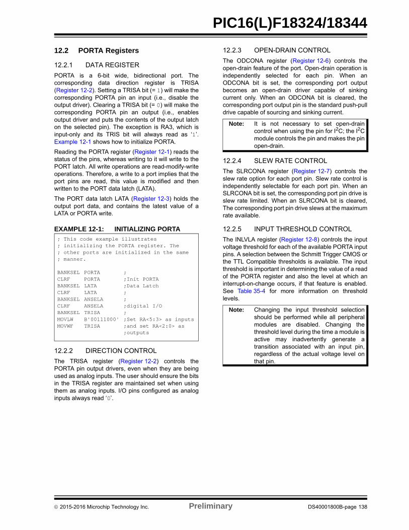
PIC16(L)F18324/18344
12.2 PORTA Registers
12.2.1 DATA REGISTER
PORTA is a 6-bit wide, bidirectional port. Thecorresponding data direction register is TRISA(Register 12-2). Setting a TRISA bit (= 1) will make thecorresponding PORTA pin an input (i.e., disable theoutput driver). Clearing a TRISA bit (= 0) will make thecorresponding PORTA pin an output (i.e., enablesoutput driver and puts the contents of the output latchon the selected pin). The exception is RA3, which isinput-only and its TRIS bit will always read as ‘1’.Example 12-1 shows how to initialize PORTA.
Reading the PORTA register (Register 12-1) reads thestatus of the pins, whereas writing to it will write to thePORT latch. All write operations are read-modify-writeoperations. Therefore, a write to a port implies that theport pins are read, this value is modified and thenwritten to the PORT data latch (LATA).
The PORT data latch LATA (Register 12-3) holds theoutput port data, and contains the latest value of aLATA or PORTA write.
EXAMPLE 12-1: INITIALIZING PORTA
12.2.2 DIRECTION CONTROL
The TRISA register (Register 12-2) controls thePORTA pin output drivers, even when they are beingused as analog inputs. The user should ensure the bitsin the TRISA register are maintained set when usingthem as analog inputs. I/O pins configured as analoginputs always read ‘0’.
12.2.3 OPEN-DRAIN CONTROL
The ODCONA register (Register 12-6) controls theopen-drain feature of the port. Open-drain operation isindependently selected for each pin. When anODCONA bit is set, the corresponding port outputbecomes an open-drain driver capable of sinkingcurrent only. When an ODCONA bit is cleared, thecorresponding port output pin is the standard push-pulldrive capable of sourcing and sinking current.
12.2.4 SLEW RATE CONTROL
The SLRCONA register (Register 12-7) controls theslew rate option for each port pin. Slew rate control isindependently selectable for each port pin. When anSLRCONA bit is set, the corresponding port pin drive isslew rate limited. When an SLRCONA bit is cleared,The corresponding port pin drive slews at the maximumrate available.
12.2.5 INPUT THRESHOLD CONTROL
The INLVLA register (Register 12-8) controls the inputvoltage threshold for each of the available PORTA inputpins. A selection between the Schmitt Trigger CMOS orthe TTL Compatible thresholds is available. The inputthreshold is important in determining the value of a readof the PORTA register and also the level at which aninterrupt-on-change occurs, if that feature is enabled.See Table 35-4 for more information on thresholdlevels.
; This code example illustrates; initializing the PORTA register. The ; other ports are initialized in the same; manner.
BANKSEL PORTA ;CLRF PORTA ;Init PORTABANKSEL LATA ;Data LatchCLRF LATA ;BANKSEL ANSELA ;CLRF ANSELA ;digital I/OBANKSEL TRISA ;MOVLW B'00111000' ;Set RA<5:3> as inputsMOVWF TRISA ;and set RA<2:0> as
;outputs
Note: It is not necessary to set open-draincontrol when using the pin for I2C; the I2Cmodule controls the pin and makes the pinopen-drain.
Note: Changing the input threshold selectionshould be performed while all peripheralmodules are disabled. Changing thethreshold level during the time a module isactive may inadvertently generate atransition associated with an input pin,regardless of the actual voltage level onthat pin.
2015-2016 Microchip Technology Inc. Preliminary DS40001800B-page 138
PIC16(L)F18324/18344
12.2.6 ANALOG CONTROL
The ANSELA register (Register 12-4) is used toconfigure the Input mode of an I/O pin to analog.Setting the appropriate ANSELA bit high will cause alldigital reads on the pin to be read as ‘0’ and allowanalog functions on the pin to operate correctly.
The state of the ANSELA bits has no effect on digitaloutput functions. A pin with TRIS clear and ANSEL setwill still operate as a digital output, but the Input modewill be analog. This can cause unexpected behaviorwhen executing read-modify-write instructions on theaffected port.
12.2.7 WEAK PULL-UP CONTROL
The WPUA register (Register 12-5) controls theindividual weak pull-ups for each port pin.
PORTA pin RA3 includes the MCLR/VPP input. TheMCLR input allows the device to be reset, and can bedisabled by the MCLRE bit of Configuration Word 2. Aweak pull-up is present on the RA3 port pin. This weakpull-up is enabled when MCLR is enabled (MCLRE = 1)or the WPUA3 bit is set. The weak pull-up is disabledwhen is disabled and the WPUA3 bit is clear.
12.2.8 PORTA FUNCTIONS AND OUTPUT PRIORITIES
Each PORTA pin is multiplexed with other functions.
Each pin defaults to the PORT latch data after Reset.Other output functions are selected with the peripheralpin select logic. See Section 13.0 “Peripheral PinSelect (PPS) Module” for more information.
Analog input functions, such as ADC and comparatorinputs are not shown in the peripheral pin select lists.Digital output functions may continue to control the pinwhen it is in Analog mode.
Note: The ANSELA bits default to the Analogmode after Reset. To use any pins asdigital general purpose or peripheralinputs, the corresponding ANSEL bitsmust be initialized to ‘0’ by user software.
2015-2016 Microchip Technology Inc. Preliminary DS40001800B-page 139
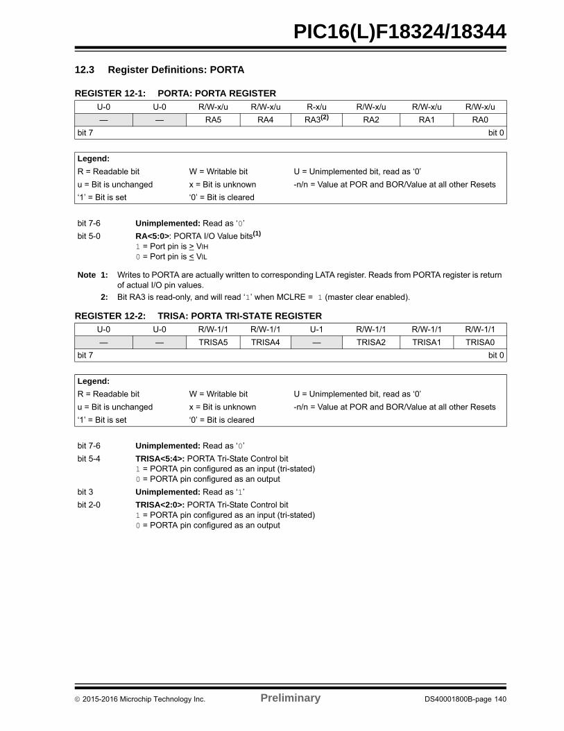
PIC16(L)F18324/18344
12.3 Register Definitions: PORTA
REGISTER 12-1: PORTA: PORTA REGISTER
U-0 U-0 R/W-x/u R/W-x/u R-x/u R/W-x/u R/W-x/u R/W-x/u
— — RA5 RA4 RA3(2) RA2 RA1 RA0
bit 7 bit 0
Legend:
R = Readable bit W = Writable bit U = Unimplemented bit, read as ‘0’
u = Bit is unchanged x = Bit is unknown -n/n = Value at POR and BOR/Value at all other Resets
‘1’ = Bit is set ‘0’ = Bit is cleared
bit 7-6 Unimplemented: Read as ‘0’
bit 5-0 RA<5:0>: PORTA I/O Value bits(1)
1 = Port pin is > VIH
0 = Port pin is < VIL
Note 1: Writes to PORTA are actually written to corresponding LATA register. Reads from PORTA register is return of actual I/O pin values.
2: Bit RA3 is read-only, and will read ‘1’ when MCLRE = 1 (master clear enabled).
REGISTER 12-2: TRISA: PORTA TRI-STATE REGISTER
U-0 U-0 R/W-1/1 R/W-1/1 U-1 R/W-1/1 R/W-1/1 R/W-1/1
— — TRISA5 TRISA4 — TRISA2 TRISA1 TRISA0
bit 7 bit 0
Legend:
R = Readable bit W = Writable bit U = Unimplemented bit, read as ‘0’
u = Bit is unchanged x = Bit is unknown -n/n = Value at POR and BOR/Value at all other Resets
‘1’ = Bit is set ‘0’ = Bit is cleared
bit 7-6 Unimplemented: Read as ‘0’
bit 5-4 TRISA<5:4>: PORTA Tri-State Control bit1 = PORTA pin configured as an input (tri-stated)0 = PORTA pin configured as an output
bit 3 Unimplemented: Read as ‘1’
bit 2-0 TRISA<2:0>: PORTA Tri-State Control bit1 = PORTA pin configured as an input (tri-stated)0 = PORTA pin configured as an output
2015-2016 Microchip Technology Inc. Preliminary DS40001800B-page 140

PIC16(L)F18324/18344
REGISTER 12-3: LATA: PORTA DATA LATCH REGISTER
U-0 U-0 R/W-x/u R/W-x/u U-0 R/W-x/u R/W-x/u R/W-x/u
— — LATA5 LATA4 — LATA2 LATA1 LATA0
bit 7 bit 0
Legend:
R = Readable bit W = Writable bit U = Unimplemented bit, read as ‘0’
u = Bit is unchanged x = Bit is unknown -n/n = Value at POR and BOR/Value at all other Resets
‘1’ = Bit is set ‘0’ = Bit is cleared
bit 7-6 Unimplemented: Read as ‘0’
bit 5-4 LATA<5:4>: RA<5:4> Output Latch Value bits(1)
bit 3 Unimplemented: Read as ‘0’
bit 2-0 LATA<2:0>: RA<2:0> Output Latch Value bits(1)
Note 1: Writes to PORTA are actually written to corresponding LATA register. Reads from PORTA register is return of actual I/O pin values.
REGISTER 12-4: ANSELA: PORTA ANALOG SELECT REGISTER
U-0 U-0 R/W-1/1 R/W-1/1 U-0 R/W-1/1 R/W-1/1 R/W-1/1
— — ANSA5 ANSA4 — ANSA2 ANSA1 ANSA0
bit 7 bit 0
Legend:
R = Readable bit W = Writable bit U = Unimplemented bit, read as ‘0’
u = Bit is unchanged x = Bit is unknown -n/n = Value at POR and BOR/Value at all other Resets
‘1’ = Bit is set ‘0’ = Bit is cleared
bit 7-6 Unimplemented: Read as ‘0’
bit 5-4 ANSA<5:4>: Analog Select between Analog or Digital Function on pins RA<5:4>, respectively1 = Analog input. Pin is assigned as analog input(1). Digital input buffer disabled.0 = Digital I/O. Pin is assigned to port or digital special function.
bit 3 Unimplemented: Read as ‘0’
bit 2-0 ANSA<2:0>: Analog Select between Analog or Digital Function on pins RA<2:0>, respectively1 = Analog input. Pin is assigned as analog input(1). Digital input buffer disabled.0 = Digital I/O. Pin is assigned to port or digital special function.
Note 1: When setting a pin to an analog input, the corresponding TRIS bit must be set to Input mode in order to allow external control of the voltage on the pin.
2015-2016 Microchip Technology Inc. Preliminary DS40001800B-page 141

PIC16(L)F18324/18344
REGISTER 12-5: WPUA: WEAK PULL-UP PORTA REGISTER
U-0 U-0 R/W-0/0 R/W-0/0 R/W-0/0 R/W-0/0 R/W-0/0 R/W-0/0
— — WPUA5 WPUA4 WPUA3(1) WPUA2 WPUA1 WPUA0
bit 7 bit 0
Legend:
R = Readable bit W = Writable bit U = Unimplemented bit, read as ‘0’
u = Bit is unchanged x = Bit is unknown -n/n = Value at POR and BOR/Value at all other Resets
‘1’ = Bit is set ‘0’ = Bit is cleared
bit 7-6 Unimplemented: Read as ‘0’
bit 5-0 WPUA<5:0>: Weak Pull-up Register bits(2)
1 = Pull-up enabled0 = Pull-up disabled
Note 1: If MCLRE = 1, the weak pull-up in RA3 is always enabled; bit WPUA3 is not affected.
2: The weak pull-up is disabled if the pin is configured as an output except when the pin is also configured as open-drain. When configured as open-drain, the pull-up is enabled when the output value is high, and disabled when the output value is low.
REGISTER 12-6: ODCONA: PORTA OPEN-DRAIN CONTROL REGISTER
U-0 U-0 R/W-0/0 R/W-0/0 U-0 R/W-0/0 R/W-0/0 R/W-0/0
— — ODCA5 ODCA4 — ODCA2 ODCA1 ODCA0
bit 7 bit 0
Legend:
R = Readable bit W = Writable bit U = Unimplemented bit, read as ‘0’
u = Bit is unchanged x = Bit is unknown -n/n = Value at POR and BOR/Value at all other Resets
‘1’ = Bit is set ‘0’ = Bit is cleared
bit 7-6 Unimplemented: Read as ‘0’
bit 5-4 ODCA<5:4>: PORTA Open-Drain Enable bitsFor RA<5:4> pins, respectively1 = Port pin operates as open-drain drive (sink current only)0 = Port pin operates as standard push-pull drive (source and sink current)
bit 3 Unimplemented: Read as ‘0’
bit 2-0 ODCA<2:0>: PORTA Open-Drain Enable bitsFor RA<2:0> pins, respectively1 = Port pin operates as open-drain drive (sink current only)0 = Port pin operates as standard push-pull drive (source and sink current)
2015-2016 Microchip Technology Inc. Preliminary DS40001800B-page 142
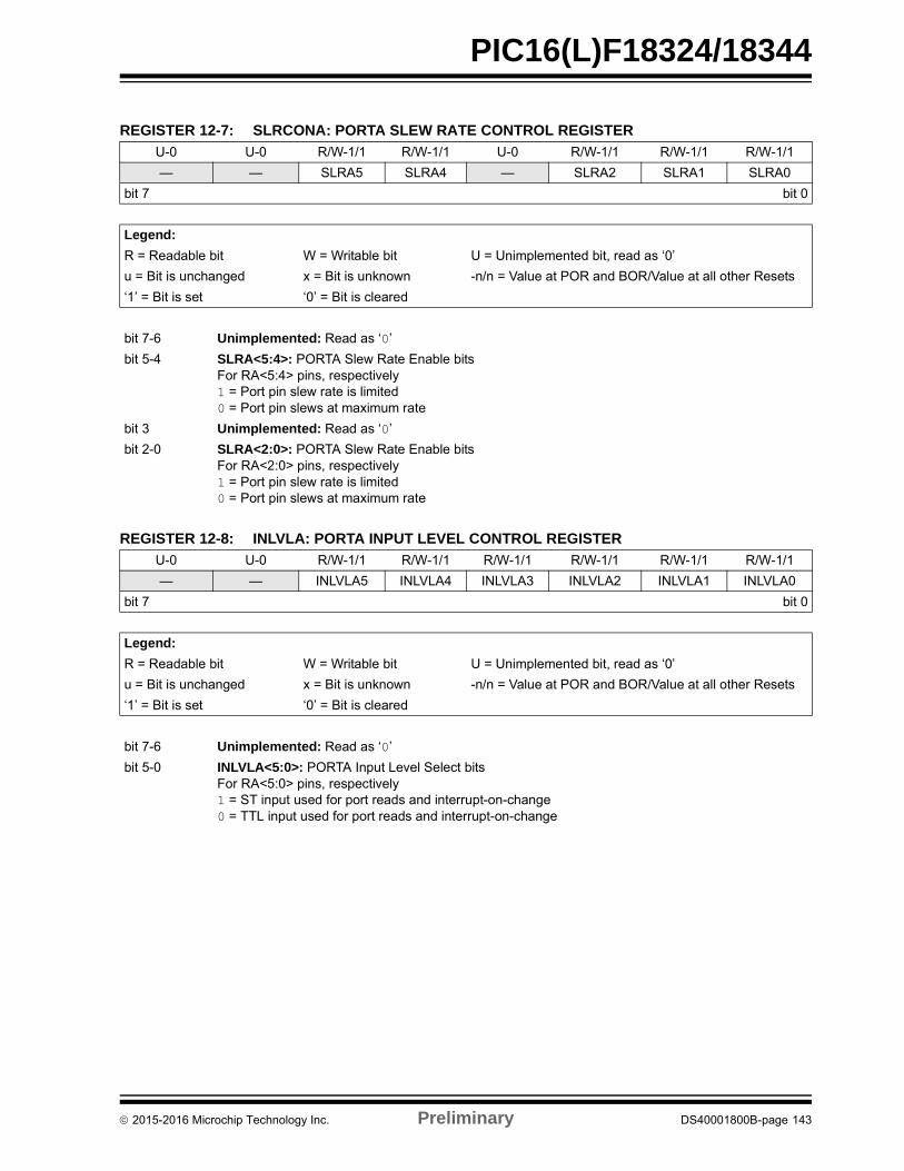
PIC16(L)F18324/18344
REGISTER 12-7: SLRCONA: PORTA SLEW RATE CONTROL REGISTER
U-0 U-0 R/W-1/1 R/W-1/1 U-0 R/W-1/1 R/W-1/1 R/W-1/1
— — SLRA5 SLRA4 — SLRA2 SLRA1 SLRA0
bit 7 bit 0
Legend:
R = Readable bit W = Writable bit U = Unimplemented bit, read as ‘0’
u = Bit is unchanged x = Bit is unknown -n/n = Value at POR and BOR/Value at all other Resets
‘1’ = Bit is set ‘0’ = Bit is cleared
bit 7-6 Unimplemented: Read as ‘0’
bit 5-4 SLRA<5:4>: PORTA Slew Rate Enable bitsFor RA<5:4> pins, respectively1 = Port pin slew rate is limited0 = Port pin slews at maximum rate
bit 3 Unimplemented: Read as ‘0’
bit 2-0 SLRA<2:0>: PORTA Slew Rate Enable bitsFor RA<2:0> pins, respectively1 = Port pin slew rate is limited0 = Port pin slews at maximum rate
REGISTER 12-8: INLVLA: PORTA INPUT LEVEL CONTROL REGISTER
U-0 U-0 R/W-1/1 R/W-1/1 R/W-1/1 R/W-1/1 R/W-1/1 R/W-1/1
— — INLVLA5 INLVLA4 INLVLA3 INLVLA2 INLVLA1 INLVLA0
bit 7 bit 0
Legend:
R = Readable bit W = Writable bit U = Unimplemented bit, read as ‘0’
u = Bit is unchanged x = Bit is unknown -n/n = Value at POR and BOR/Value at all other Resets
‘1’ = Bit is set ‘0’ = Bit is cleared
bit 7-6 Unimplemented: Read as ‘0’
bit 5-0 INLVLA<5:0>: PORTA Input Level Select bitsFor RA<5:0> pins, respectively1 = ST input used for port reads and interrupt-on-change0 = TTL input used for port reads and interrupt-on-change
2015-2016 Microchip Technology Inc. Preliminary DS40001800B-page 143
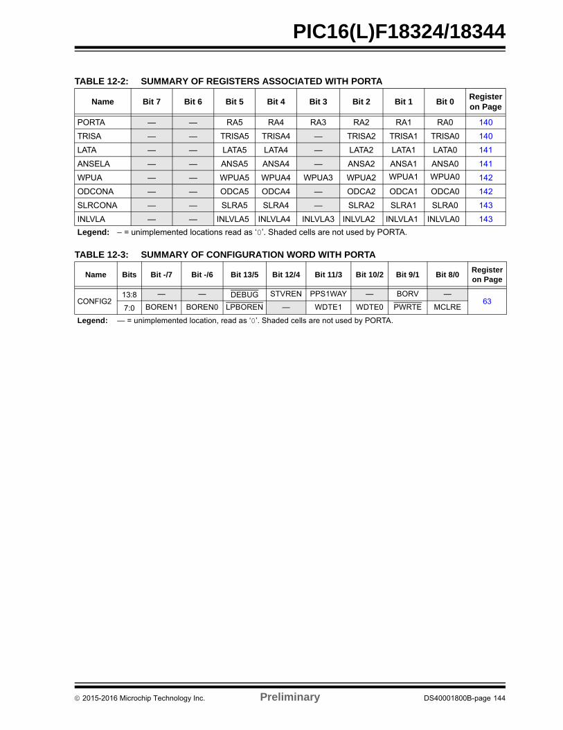
PIC16(L)F18324/18344
TABLE 12-3: SUMMARY OF CONFIGURATION WORD WITH PORTA
TABLE 12-2: SUMMARY OF REGISTERS ASSOCIATED WITH PORTA
Name Bit 7 Bit 6 Bit 5 Bit 4 Bit 3 Bit 2 Bit 1 Bit 0Register on Page
PORTA — — RA5 RA4 RA3 RA2 RA1 RA0 140
TRISA — — TRISA5 TRISA4 — TRISA2 TRISA1 TRISA0 140
LATA — — LATA5 LATA4 — LATA2 LATA1 LATA0 141
ANSELA — — ANSA5 ANSA4 — ANSA2 ANSA1 ANSA0 141
WPUA — — WPUA5 WPUA4 WPUA3 WPUA2 WPUA1 WPUA0 142
ODCONA — — ODCA5 ODCA4 — ODCA2 ODCA1 ODCA0 142
SLRCONA — — SLRA5 SLRA4 — SLRA2 SLRA1 SLRA0 143
INLVLA — — INLVLA5 INLVLA4 INLVLA3 INLVLA2 INLVLA1 INLVLA0 143
Legend: – = unimplemented locations read as ‘0’. Shaded cells are not used by PORTA.
Name Bits Bit -/7 Bit -/6 Bit 13/5 Bit 12/4 Bit 11/3 Bit 10/2 Bit 9/1 Bit 8/0Register on Page
CONFIG213:8 — — DEBUG STVREN PPS1WAY — BORV —
637:0 BOREN1 BOREN0 LPBOREN — WDTE1 WDTE0 PWRTE MCLRE
Legend: — = unimplemented location, read as ‘0’. Shaded cells are not used by PORTA.
2015-2016 Microchip Technology Inc. Preliminary DS40001800B-page 144
PIC16(L)F18324/18344
12.4 PORTB Registers (PIC16(L)F18344 Only)
12.4.1 DATA REGISTER
PORTB is a 4-bit wide bidirectional port and is onlyavailable in the PIC16(L)F18344 devices. Thecorresponding data direction register is TRISB(Register 12-10). Setting a TRISB bit (= 1) will makethe corresponding PORTB pin an input (i.e., put thecorresponding output driver in a High-Impedancemode). Clearing a TRISB bit (= 0) will make thecorresponding PORTB pin an output (i.e., enable theoutput driver and put the contents of the output latch onthe selected pin). Example 12-1 shows how to initializean I/O port.
Reading the PORTB register (Register 12-9) reads thestatus of the pins, whereas writing to it will write to thePORT latch. All write operations are read-modify-writeoperations. Therefore, a write to a port implies that theport pins are read; this value is modified and thenwritten to the PORT data latch (LATB).
The PORT data latch LATB (Register 12-11) holds theoutput port data, and contains the latest value of aLATB or PORTB write.
12.4.2 DIRECTION CONTROL
The TRISB register (Register 12-10) controls thePORTB pin output drivers, even when they are beingused as analog inputs. The user should ensure the bitsin the TRISB register are maintained set when usingthem as analog inputs. I/O pins configured as analoginputs always read ‘0’.
12.4.3 INPUT THRESHOLD CONTROL
The INLVLB register (Register 12-16) controls the inputvoltage threshold for each of the available PORTBinput pins. A selection between the Schmitt TriggerCMOS or the TTL Compatible thresholds is available.The input threshold is important in determining thevalue of a read of the PORTB register and also the levelat which an interrupt-on-change occurs, if that featureis enabled. See Table 35-4 for more information onthreshold levels.
12.4.4 OPEN-DRAIN CONTROL
The ODCONB register (Register 12-14) controls theopen-drain feature of the port. Open-drain operation isindependently selected for each pin. When anODCONB bit is set, the corresponding port outputbecomes an open-drain driver capable of sinkingcurrent only. When an ODCONB bit is cleared, thecorresponding port output pin is the standard push-pulldrive capable of sourcing and sinking current.
12.4.5 SLEW RATE CONTROL
The SLRCONB register (Register 12-15) controls theslew rate option for each port pin. Slew rate control isindependently selectable for each port pin. When anSLRCONB bit is set, the corresponding port pin drive isslew rate limited. When an SLRCONB bit is cleared,the corresponding port pin drive slews at the maximumrate available.
12.4.6 ANALOG CONTROL
The ANSELB register (Register 12-12) is used toconfigure the Input mode of an I/O pin to analog.Setting the appropriate ANSELB bit high will cause alldigital reads on the pin to be read as ‘0’ and allowanalog functions on the pin to operate correctly.
The state of the ANSELB bits has no effect on digitaloutput functions. A pin with TRIS clear and ANSELBset will still operate as a digital output, but the Inputmode will be analog. This can cause unexpectedbehavior when executing read-modify-writeinstructions on the affected port.
12.4.7 WEAK PULL-UP CONTROL
The WPUB register (Register 12-13) controls theindividual weak pull-ups for each port pin.
12.4.8 PORTB FUNCTIONS AND OUTPUT PRIORITIES
Each pin defaults to the PORT latch data after Reset.Other output functions are selected with the peripheralpin select logic. See Section 13.0 “Peripheral PinSelect (PPS) Module” for more information.
Analog input functions, such as ADC and comparatorinputs, are not shown in the peripheral pin select lists.Digital output functions may continue to control the pinwhen it is in Analog mode.
Note: Changing the input threshold selectionshould be performed while all peripheralmodules are disabled. Changing thethreshold level during the time a module isactive may inadvertently generate atransition associated with an input pin,regardless of the actual voltage level onthat pin.
Note: It is not necessary to set open-draincontrol when using the pin for I2C; the I2Cmodule controls the pin and makes the pinopen-drain.
Note: The ANSELB bits default to the Analogmode after Reset. To use any pins asdigital general purpose or peripheralinputs, the corresponding ANSEL bitsmust be initialized to ‘0’ by user software.
2015-2016 Microchip Technology Inc. Preliminary DS40001800B-page 145
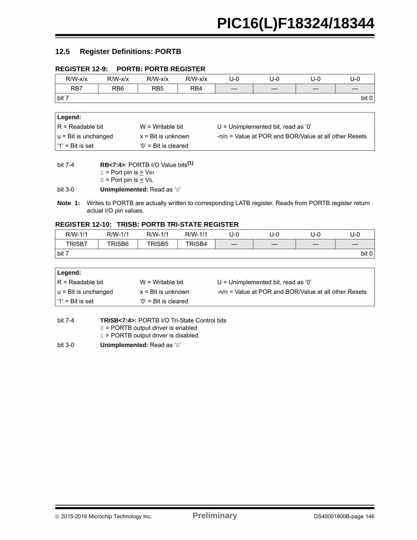
PIC16(L)F18324/18344
12.5 Register Definitions: PORTB
REGISTER 12-9: PORTB: PORTB REGISTER
R/W-x/x R/W-x/x R/W-x/x R/W-x/x U-0 U-0 U-0 U-0
RB7 RB6 RB5 RB4 — — — —
bit 7 bit 0
Legend:
R = Readable bit W = Writable bit U = Unimplemented bit, read as ‘0’
u = Bit is unchanged x = Bit is unknown -n/n = Value at POR and BOR/Value at all other Resets
‘1’ = Bit is set ‘0’ = Bit is cleared
bit 7-4 RB<7:4>: PORTB I/O Value bits(1)
1 = Port pin is > VIH
0 = Port pin is < VIL
bit 3-0 Unimplemented: Read as ‘0’
Note 1: Writes to PORTB are actually written to corresponding LATB register. Reads from PORTB register return actual I/O pin values.
REGISTER 12-10: TRISB: PORTB TRI-STATE REGISTER
R/W-1/1 R/W-1/1 R/W-1/1 R/W-1/1 U-0 U-0 U-0 U-0
TRISB7 TRISB6 TRISB5 TRISB4 — — — —
bit 7 bit 0
Legend:
R = Readable bit W = Writable bit U = Unimplemented bit, read as ‘0’
u = Bit is unchanged x = Bit is unknown -n/n = Value at POR and BOR/Value at all other Resets
‘1’ = Bit is set ‘0’ = Bit is cleared
bit 7-4 TRISB<7:4>: PORTB I/O Tri-State Control bits0 = PORTB output driver is enabled1 = PORTB output driver is disabled
bit 3-0 Unimplemented: Read as ‘0’
2015-2016 Microchip Technology Inc. Preliminary DS40001800B-page 146
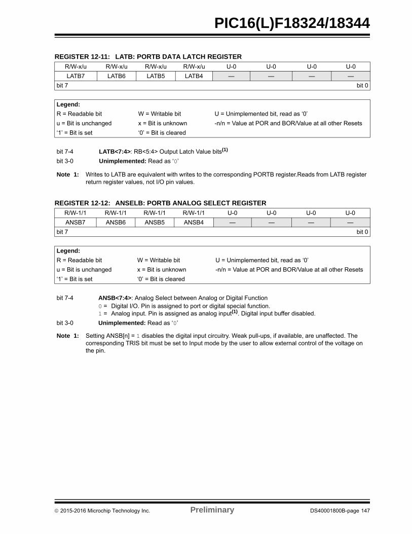
PIC16(L)F18324/18344
REGISTER 12-11: LATB: PORTB DATA LATCH REGISTER
R/W-x/u R/W-x/u R/W-x/u R/W-x/u U-0 U-0 U-0 U-0
LATB7 LATB6 LATB5 LATB4 — — — —
bit 7 bit 0
Legend:
R = Readable bit W = Writable bit U = Unimplemented bit, read as ‘0’
u = Bit is unchanged x = Bit is unknown -n/n = Value at POR and BOR/Value at all other Resets
‘1’ = Bit is set ‘0’ = Bit is cleared
bit 7-4 LATB<7:4>: RB<5:4> Output Latch Value bits(1)
bit 3-0 Unimplemented: Read as ‘0’
Note 1: Writes to LATB are equivalent with writes to the corresponding PORTB register.Reads from LATB register return register values, not I/O pin values.
REGISTER 12-12: ANSELB: PORTB ANALOG SELECT REGISTER
R/W-1/1 R/W-1/1 R/W-1/1 R/W-1/1 U-0 U-0 U-0 U-0
ANSB7 ANSB6 ANSB5 ANSB4 — — — —
bit 7 bit 0
Legend:
R = Readable bit W = Writable bit U = Unimplemented bit, read as ‘0’
u = Bit is unchanged x = Bit is unknown -n/n = Value at POR and BOR/Value at all other Resets
‘1’ = Bit is set ‘0’ = Bit is cleared
bit 7-4 ANSB<7:4>: Analog Select between Analog or Digital Function0 = Digital I/O. Pin is assigned to port or digital special function.1 = Analog input. Pin is assigned as analog input(1). Digital input buffer disabled.
bit 3-0 Unimplemented: Read as ‘0’
Note 1: Setting ANSB[n] = 1 disables the digital input circuitry. Weak pull-ups, if available, are unaffected. The corresponding TRIS bit must be set to Input mode by the user to allow external control of the voltage on the pin.
2015-2016 Microchip Technology Inc. Preliminary DS40001800B-page 147
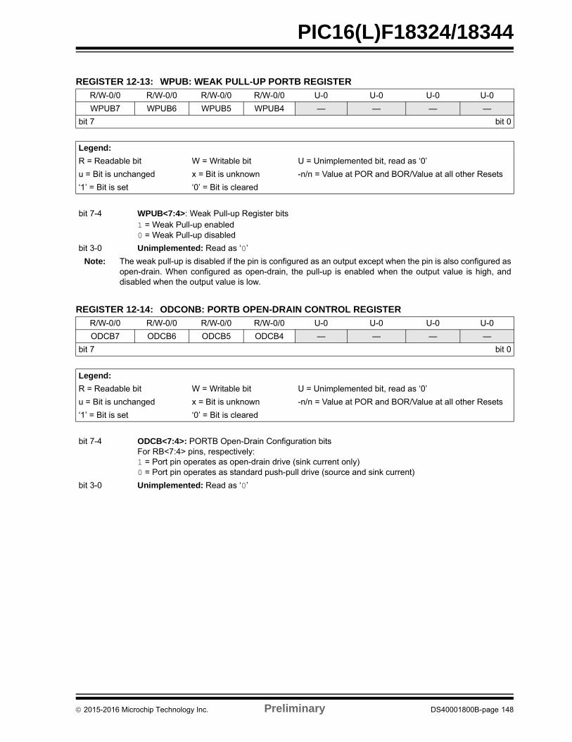
PIC16(L)F18324/18344
REGISTER 12-13: WPUB: WEAK PULL-UP PORTB REGISTER
R/W-0/0 R/W-0/0 R/W-0/0 R/W-0/0 U-0 U-0 U-0 U-0
WPUB7 WPUB6 WPUB5 WPUB4 — — — —
bit 7 bit 0
Legend:
R = Readable bit W = Writable bit U = Unimplemented bit, read as ‘0’
u = Bit is unchanged x = Bit is unknown -n/n = Value at POR and BOR/Value at all other Resets
‘1’ = Bit is set ‘0’ = Bit is cleared
bit 7-4 WPUB<7:4>: Weak Pull-up Register bits1 = Weak Pull-up enabled0 = Weak Pull-up disabled
bit 3-0 Unimplemented: Read as ‘0’
Note: The weak pull-up is disabled if the pin is configured as an output except when the pin is also configured asopen-drain. When configured as open-drain, the pull-up is enabled when the output value is high, anddisabled when the output value is low.
REGISTER 12-14: ODCONB: PORTB OPEN-DRAIN CONTROL REGISTER
R/W-0/0 R/W-0/0 R/W-0/0 R/W-0/0 U-0 U-0 U-0 U-0
ODCB7 ODCB6 ODCB5 ODCB4 — — — —
bit 7 bit 0
Legend:
R = Readable bit W = Writable bit U = Unimplemented bit, read as ‘0’
u = Bit is unchanged x = Bit is unknown -n/n = Value at POR and BOR/Value at all other Resets
‘1’ = Bit is set ‘0’ = Bit is cleared
bit 7-4 ODCB<7:4>: PORTB Open-Drain Configuration bitsFor RB<7:4> pins, respectively:1 = Port pin operates as open-drain drive (sink current only)0 = Port pin operates as standard push-pull drive (source and sink current)
bit 3-0 Unimplemented: Read as ‘0’
2015-2016 Microchip Technology Inc. Preliminary DS40001800B-page 148
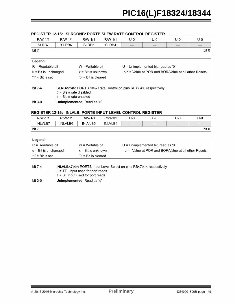
PIC16(L)F18324/18344
REGISTER 12-15: SLRCONB: PORTB SLEW RATE CONTROL REGISTER
R/W-1/1 R/W-1/1 R/W-1/1 R/W-1/1 U-0 U-0 U-0 U-0
SLRB7 SLRB6 SLRB5 SLRB4 — — — —
bit 7 bit 0
Legend:
R = Readable bit W = Writable bit U = Unimplemented bit, read as ‘0’
u = Bit is unchanged x = Bit is unknown -n/n = Value at POR and BOR/Value at all other Resets
‘1’ = Bit is set ‘0’ = Bit is cleared
bit 7-4 SLRB<7:4>: PORTB Slew Rate Control on pins RB<7:4>, respectively0 = Slew rate disabled1 = Slew rate enabled
bit 3-0 Unimplemented: Read as ‘0’
REGISTER 12-16: INLVLB: PORTB INPUT LEVEL CONTROL REGISTER
R/W-1/1 R/W-1/1 R/W-1/1 R/W-1/1 U-0 U-0 U-0 U-0
INLVLB7 INLVLB6 INLVLB5 INLVLB4 — — — —
bit 7 bit 0
Legend:
R = Readable bit W = Writable bit U = Unimplemented bit, read as ‘0’
u = Bit is unchanged x = Bit is unknown -n/n = Value at POR and BOR/Value at all other Resets
‘1’ = Bit is set ‘0’ = Bit is cleared
bit 7-4 INLVLB<7:4>: PORTB Input Level Select on pins RB<7:4>, respectively0 = TTL input used for port reads1 = ST input used for port reads
bit 3-0 Unimplemented: Read as ‘0’
2015-2016 Microchip Technology Inc. Preliminary DS40001800B-page 149
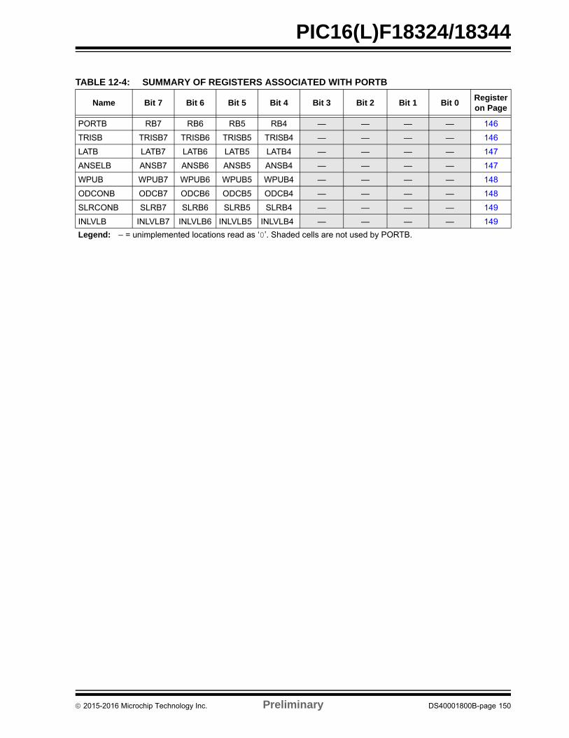
PIC16(L)F18324/18344
TABLE 12-4: SUMMARY OF REGISTERS ASSOCIATED WITH PORTB
Name Bit 7 Bit 6 Bit 5 Bit 4 Bit 3 Bit 2 Bit 1 Bit 0Register on Page
PORTB RB7 RB6 RB5 RB4 — — — — 146
TRISB TRISB7 TRISB6 TRISB5 TRISB4 — — — — 146
LATB LATB7 LATB6 LATB5 LATB4 — — — — 147
ANSELB ANSB7 ANSB6 ANSB5 ANSB4 — — — — 147
WPUB WPUB7 WPUB6 WPUB5 WPUB4 — — — — 148
ODCONB ODCB7 ODCB6 ODCB5 ODCB4 — — — — 148
SLRCONB SLRB7 SLRB6 SLRB5 SLRB4 — — — — 149
INLVLB INLVLB7 INLVLB6 INLVLB5 INLVLB4 — — — — 149
Legend: – = unimplemented locations read as ‘0’. Shaded cells are not used by PORTB.
2015-2016 Microchip Technology Inc. Preliminary DS40001800B-page 150
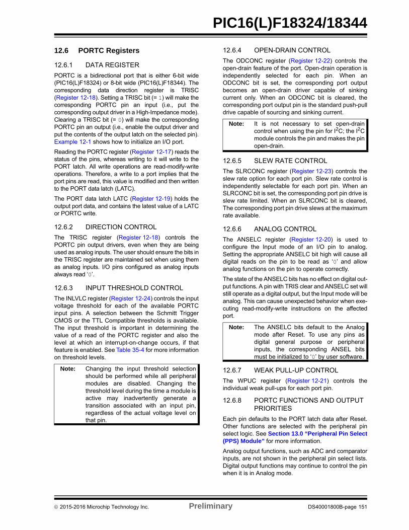
PIC16(L)F18324/18344
12.6 PORTC Registers
12.6.1 DATA REGISTER
PORTC is a bidirectional port that is either 6-bit wide(PIC16(L)F18324) or 8-bit wide (PIC16(L)F18344). Thecorresponding data direction register is TRISC(Register 12-18). Setting a TRISC bit (= 1) will make thecorresponding PORTC pin an input (i.e., put thecorresponding output driver in a High-Impedance mode).Clearing a TRISC bit (= 0) will make the correspondingPORTC pin an output (i.e., enable the output driver andput the contents of the output latch on the selected pin).Example 12-1 shows how to initialize an I/O port.
Reading the PORTC register (Register 12-17) reads thestatus of the pins, whereas writing to it will write to thePORT latch. All write operations are read-modify-writeoperations. Therefore, a write to a port implies that theport pins are read, this value is modified and then writtento the PORT data latch (LATC).
The PORT data latch LATC (Register 12-19) holds theoutput port data, and contains the latest value of a LATCor PORTC write.
12.6.2 DIRECTION CONTROL
The TRISC register (Register 12-18) controls thePORTC pin output drivers, even when they are beingused as analog inputs. The user should ensure the bits inthe TRISC register are maintained set when using themas analog inputs. I/O pins configured as analog inputsalways read ‘0’.
12.6.3 INPUT THRESHOLD CONTROL
The INLVLC register (Register 12-24) controls the inputvoltage threshold for each of the available PORTCinput pins. A selection between the Schmitt TriggerCMOS or the TTL Compatible thresholds is available.The input threshold is important in determining thevalue of a read of the PORTC register and also thelevel at which an interrupt-on-change occurs, if thatfeature is enabled. See Table 35-4 for more informationon threshold levels.
12.6.4 OPEN-DRAIN CONTROL
The ODCONC register (Register 12-22) controls theopen-drain feature of the port. Open-drain operation isindependently selected for each pin. When anODCONC bit is set, the corresponding port outputbecomes an open-drain driver capable of sinkingcurrent only. When an ODCONC bit is cleared, thecorresponding port output pin is the standard push-pulldrive capable of sourcing and sinking current.
12.6.5 SLEW RATE CONTROL
The SLRCONC register (Register 12-23) controls theslew rate option for each port pin. Slew rate control isindependently selectable for each port pin. When anSLRCONC bit is set, the corresponding port pin drive isslew rate limited. When an SLRCONC bit is cleared,The corresponding port pin drive slews at the maximumrate available.
12.6.6 ANALOG CONTROL
The ANSELC register (Register 12-20) is used toconfigure the Input mode of an I/O pin to analog.Setting the appropriate ANSELC bit high will cause alldigital reads on the pin to be read as ‘0’ and allowanalog functions on the pin to operate correctly.
The state of the ANSELC bits has no effect on digital out-put functions. A pin with TRIS clear and ANSELC set willstill operate as a digital output, but the Input mode will beanalog. This can cause unexpected behavior when exe-cuting read-modify-write instructions on the affectedport.
12.6.7 WEAK PULL-UP CONTROL
The WPUC register (Register 12-21) controls theindividual weak pull-ups for each port pin.
12.6.8 PORTC FUNCTIONS AND OUTPUT PRIORITIES
Each pin defaults to the PORT latch data after Reset.Other functions are selected with the peripheral pinselect logic. See Section 13.0 “Peripheral Pin Select(PPS) Module” for more information.
Analog output functions, such as ADC and comparatorinputs, are not shown in the peripheral pin select lists.Digital output functions may continue to control the pinwhen it is in Analog mode.
Note: Changing the input threshold selectionshould be performed while all peripheralmodules are disabled. Changing thethreshold level during the time a module isactive may inadvertently generate atransition associated with an input pin,regardless of the actual voltage level onthat pin.
Note: It is not necessary to set open-draincontrol when using the pin for I2C; the I2Cmodule controls the pin and makes the pinopen-drain.
Note: The ANSELC bits default to the Analogmode after Reset. To use any pins asdigital general purpose or peripheralinputs, the corresponding ANSEL bitsmust be initialized to ‘0’ by user software.
2015-2016 Microchip Technology Inc. Preliminary DS40001800B-page 151
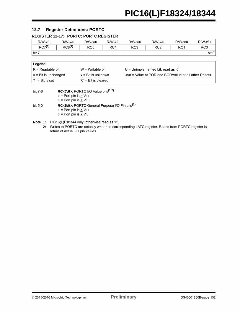
PIC16(L)F18324/18344
12.7 Register Definitions: PORTC
REGISTER 12-17: PORTC: PORTC REGISTER
R/W-x/u R/W-x/u R/W-x/u R/W-x/u R/W-x/u R/W-x/u R/W-x/u R/W-x/u
RC7(1) RC6(1) RC5 RC4 RC3 RC2 RC1 RC0
bit 7 bit 0
Legend:
R = Readable bit W = Writable bit U = Unimplemented bit, read as ‘0’
u = Bit is unchanged x = Bit is unknown -n/n = Value at POR and BOR/Value at all other Resets
‘1’ = Bit is set ‘0’ = Bit is cleared
bit 7-6 RC<7:6>: PORTC I/O Value bits(1,2)
1 = Port pin is > VIH
0 = Port pin is < VIL
bit 5-0 RC<5:0>: PORTC General Purpose I/O Pin bits(2)
1 = Port pin is > VIH
0 = Port pin is < VIL
Note 1: PIC16(L)F18344 only; otherwise read as ‘0’.2: Writes to PORTC are actually written to corresponding LATC register. Reads from PORTC register is
return of actual I/O pin values.
2015-2016 Microchip Technology Inc. Preliminary DS40001800B-page 152
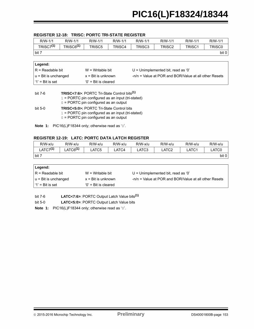
PIC16(L)F18324/18344
REGISTER 12-18: TRISC: PORTC TRI-STATE REGISTER
R/W-1/1 R/W-1/1 R/W-1/1 R/W-1/1 R/W-1/1 R/W-1/1 R/W-1/1 R/W-1/1
TRISC7(1) TRISC6(1) TRISC5 TRISC4 TRISC3 TRISC2 TRISC1 TRISC0
bit 7 bit 0
Legend:
R = Readable bit W = Writable bit U = Unimplemented bit, read as ‘0’
u = Bit is unchanged x = Bit is unknown -n/n = Value at POR and BOR/Value at all other Resets
‘1’ = Bit is set ‘0’ = Bit is cleared
bit 7-6 TRISC<7:6>: PORTC Tri-State Control bits(1)
1 = PORTC pin configured as an input (tri-stated)0 = PORTC pin configured as an output
bit 5-0 TRISC<5:0>: PORTC Tri-State Control bits1 = PORTC pin configured as an input (tri-stated)0 = PORTC pin configured as an output
Note 1: PIC16(L)F18344 only; otherwise read as ‘0’.
REGISTER 12-19: LATC: PORTC DATA LATCH REGISTER
R/W-x/u R/W-x/u R/W-x/u R/W-x/u R/W-x/u R/W-x/u R/W-x/u R/W-x/u
LATC7(1) LATC6(1) LATC5 LATC4 LATC3 LATC2 LATC1 LATC0
bit 7 bit 0
Legend:
R = Readable bit W = Writable bit U = Unimplemented bit, read as ‘0’
u = Bit is unchanged x = Bit is unknown -n/n = Value at POR and BOR/Value at all other Resets
‘1’ = Bit is set ‘0’ = Bit is cleared
bit 7-6 LATC<7:6>: PORTC Output Latch Value bits(1)
bit 5-0 LATC<5:0>: PORTC Output Latch Value bits
Note 1: PIC16(L)F18344 only; otherwise read as ‘0’.
2015-2016 Microchip Technology Inc. Preliminary DS40001800B-page 153
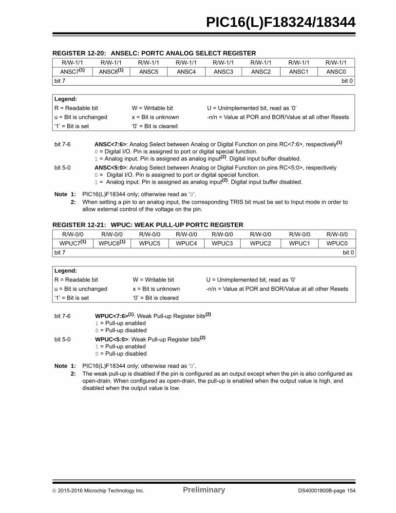
PIC16(L)F18324/18344
REGISTER 12-20: ANSELC: PORTC ANALOG SELECT REGISTER
R/W-1/1 R/W-1/1 R/W-1/1 R/W-1/1 R/W-1/1 R/W-1/1 R/W-1/1 R/W-1/1
ANSC7(1) ANSC6(1) ANSC5 ANSC4 ANSC3 ANSC2 ANSC1 ANSC0
bit 7 bit 0
Legend:
R = Readable bit W = Writable bit U = Unimplemented bit, read as ‘0’
u = Bit is unchanged x = Bit is unknown -n/n = Value at POR and BOR/Value at all other Resets
‘1’ = Bit is set ‘0’ = Bit is cleared
bit 7-6 ANSC<7:6>: Analog Select between Analog or Digital Function on pins RC<7:6>, respectively(1)
0 = Digital I/O. Pin is assigned to port or digital special function.1 = Analog input. Pin is assigned as analog input(2). Digital input buffer disabled.
bit 5-0 ANSC<5:0>: Analog Select between Analog or Digital Function on pins RC<5:0>, respectively0 = Digital I/O. Pin is assigned to port or digital special function.1 = Analog input. Pin is assigned as analog input(2). Digital input buffer disabled.
Note 1: PIC16(L)F18344 only; otherwise read as ‘0’.2: When setting a pin to an analog input, the corresponding TRIS bit must be set to Input mode in order to
allow external control of the voltage on the pin.
REGISTER 12-21: WPUC: WEAK PULL-UP PORTC REGISTER
R/W-0/0 R/W-0/0 R/W-0/0 R/W-0/0 R/W-0/0 R/W-0/0 R/W-0/0 R/W-0/0
WPUC7(1) WPUC6(1) WPUC5 WPUC4 WPUC3 WPUC2 WPUC1 WPUC0
bit 7 bit 0
Legend:
R = Readable bit W = Writable bit U = Unimplemented bit, read as ‘0’
u = Bit is unchanged x = Bit is unknown -n/n = Value at POR and BOR/Value at all other Resets
‘1’ = Bit is set ‘0’ = Bit is cleared
bit 7-6 WPUC<7:6>(1): Weak Pull-up Register bits(2)
1 = Pull-up enabled0 = Pull-up disabled
bit 5-0 WPUC<5:0>: Weak Pull-up Register bits(2)
1 = Pull-up enabled0 = Pull-up disabled
Note 1: PIC16(L)F18344 only; otherwise read as ‘0’.2: The weak pull-up is disabled if the pin is configured as an output except when the pin is also configured as
open-drain. When configured as open-drain, the pull-up is enabled when the output value is high, and disabled when the output value is low.
2015-2016 Microchip Technology Inc. Preliminary DS40001800B-page 154
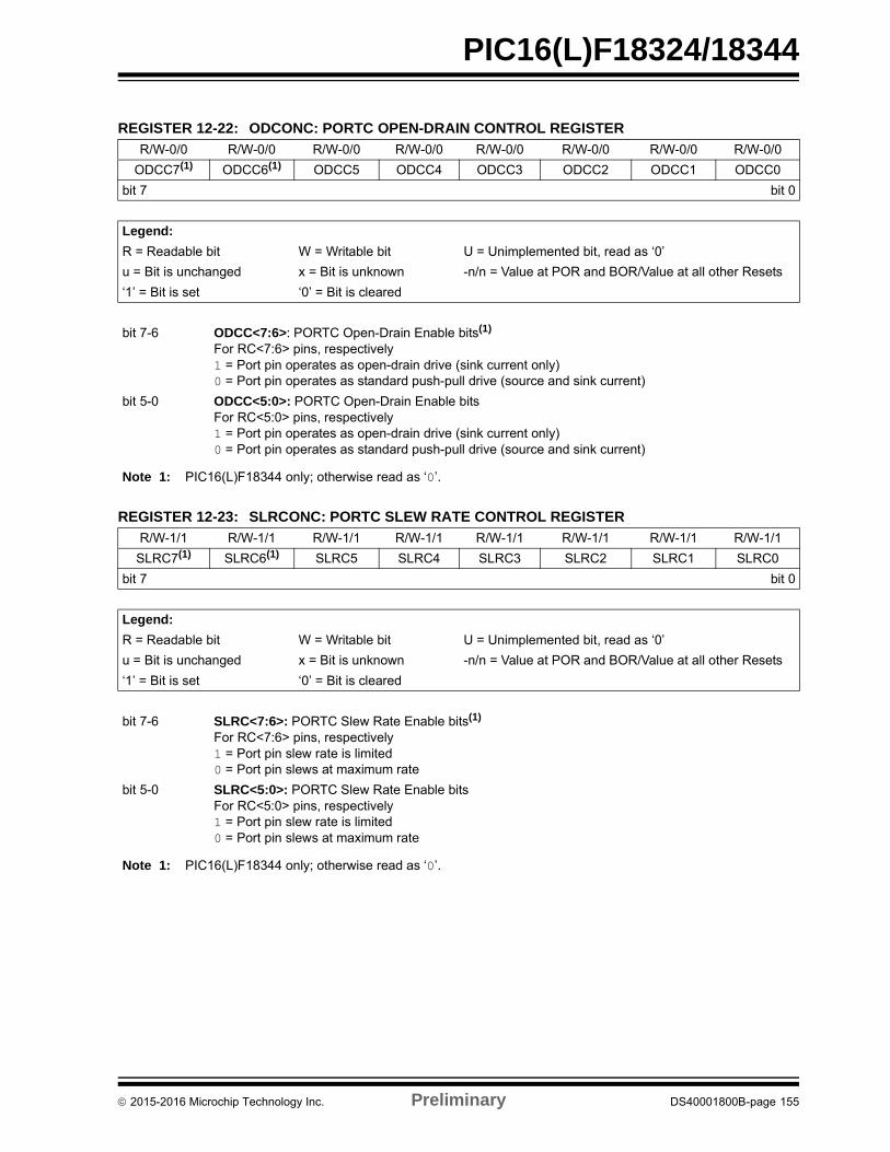
PIC16(L)F18324/18344
REGISTER 12-22: ODCONC: PORTC OPEN-DRAIN CONTROL REGISTER
R/W-0/0 R/W-0/0 R/W-0/0 R/W-0/0 R/W-0/0 R/W-0/0 R/W-0/0 R/W-0/0
ODCC7(1) ODCC6(1) ODCC5 ODCC4 ODCC3 ODCC2 ODCC1 ODCC0
bit 7 bit 0
Legend:
R = Readable bit W = Writable bit U = Unimplemented bit, read as ‘0’
u = Bit is unchanged x = Bit is unknown -n/n = Value at POR and BOR/Value at all other Resets
‘1’ = Bit is set ‘0’ = Bit is cleared
bit 7-6 ODCC<7:6>: PORTC Open-Drain Enable bits(1)
For RC<7:6> pins, respectively1 = Port pin operates as open-drain drive (sink current only)0 = Port pin operates as standard push-pull drive (source and sink current)
bit 5-0 ODCC<5:0>: PORTC Open-Drain Enable bitsFor RC<5:0> pins, respectively1 = Port pin operates as open-drain drive (sink current only)0 = Port pin operates as standard push-pull drive (source and sink current)
Note 1: PIC16(L)F18344 only; otherwise read as ‘0’.
REGISTER 12-23: SLRCONC: PORTC SLEW RATE CONTROL REGISTER
R/W-1/1 R/W-1/1 R/W-1/1 R/W-1/1 R/W-1/1 R/W-1/1 R/W-1/1 R/W-1/1
SLRC7(1) SLRC6(1) SLRC5 SLRC4 SLRC3 SLRC2 SLRC1 SLRC0
bit 7 bit 0
Legend:
R = Readable bit W = Writable bit U = Unimplemented bit, read as ‘0’
u = Bit is unchanged x = Bit is unknown -n/n = Value at POR and BOR/Value at all other Resets
‘1’ = Bit is set ‘0’ = Bit is cleared
bit 7-6 SLRC<7:6>: PORTC Slew Rate Enable bits(1)
For RC<7:6> pins, respectively1 = Port pin slew rate is limited0 = Port pin slews at maximum rate
bit 5-0 SLRC<5:0>: PORTC Slew Rate Enable bitsFor RC<5:0> pins, respectively1 = Port pin slew rate is limited0 = Port pin slews at maximum rate
Note 1: PIC16(L)F18344 only; otherwise read as ‘0’.
2015-2016 Microchip Technology Inc. Preliminary DS40001800B-page 155
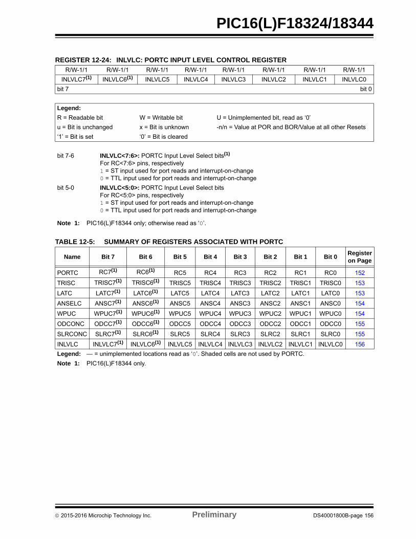
PIC16(L)F18324/18344
REGISTER 12-24: INLVLC: PORTC INPUT LEVEL CONTROL REGISTER
R/W-1/1 R/W-1/1 R/W-1/1 R/W-1/1 R/W-1/1 R/W-1/1 R/W-1/1 R/W-1/1
INLVLC7(1) INLVLC6(1) INLVLC5 INLVLC4 INLVLC3 INLVLC2 INLVLC1 INLVLC0
bit 7 bit 0
Legend:
R = Readable bit W = Writable bit U = Unimplemented bit, read as ‘0’
u = Bit is unchanged x = Bit is unknown -n/n = Value at POR and BOR/Value at all other Resets
‘1’ = Bit is set ‘0’ = Bit is cleared
bit 7-6 INLVLC<7:6>: PORTC Input Level Select bits(1)
For RC<7:6> pins, respectively1 = ST input used for port reads and interrupt-on-change0 = TTL input used for port reads and interrupt-on-change
bit 5-0 INLVLC<5:0>: PORTC Input Level Select bitsFor RC<5:0> pins, respectively1 = ST input used for port reads and interrupt-on-change0 = TTL input used for port reads and interrupt-on-change
Note 1: PIC16(L)F18344 only; otherwise read as ‘0’.
TABLE 12-5: SUMMARY OF REGISTERS ASSOCIATED WITH PORTC
Name Bit 7 Bit 6 Bit 5 Bit 4 Bit 3 Bit 2 Bit 1 Bit 0Register on Page
PORTC RC7(1) RC6(1) RC5 RC4 RC3 RC2 RC1 RC0 152
TRISC TRISC7(1) TRISC6(1) TRISC5 TRISC4 TRISC3 TRISC2 TRISC1 TRISC0 153
LATC LATC7(1) LATC6(1) LATC5 LATC4 LATC3 LATC2 LATC1 LATC0 153
ANSELC ANSC7(1) ANSC6(1) ANSC5 ANSC4 ANSC3 ANSC2 ANSC1 ANSC0 154
WPUC WPUC7(1) WPUC6(1) WPUC5 WPUC4 WPUC3 WPUC2 WPUC1 WPUC0 154
ODCONC ODCC7(1) ODCC6(1) ODCC5 ODCC4 ODCC3 ODCC2 ODCC1 ODCC0 155
SLRCONC SLRC7(1) SLRC6(1) SLRC5 SLRC4 SLRC3 SLRC2 SLRC1 SLRC0 155
INLVLC INLVLC7(1) INLVLC6(1) INLVLC5 INLVLC4 INLVLC3 INLVLC2 INLVLC1 INLVLC0 156
Legend: — = unimplemented locations read as ‘0’. Shaded cells are not used by PORTC.
Note 1: PIC16(L)F18344 only.
2015-2016 Microchip Technology Inc. Preliminary DS40001800B-page 156
PIC16(L)F18324/18344
13.0 PERIPHERAL PIN SELECT (PPS) MODULE
The Peripheral Pin Select (PPS) module connectsperipheral inputs and outputs to the device I/O pins.Only digital signals are included in the selections. Allanalog inputs and outputs remain fixed to theirassigned pins. Input and output selections areindependent as shown in the simplified block diagramFigure 13-1.
13.1 PPS Inputs
Each peripheral has a PPS register with which theinputs to the peripheral are selected. Inputs include thedevice pins.
Although every peripheral has its own PPS inputselection register, the selections are identical for everyperipheral as shown in Register 13-1.
13.2 PPS Outputs
Each I/O pin has a PPS register with which the pinoutput source is selected. With few exceptions, the portTRIS control associated with that pin retains controlover the pin output driver. Peripherals that control thepin output driver as part of the peripheral operation willoverride the TRIS control as needed. Theseperipherals are:
• EUSART (synchronous operation)
• MSSP (I2C)
Although every pin has its own PPS peripheralselection register, the selections are identical for everypin as shown in Register 13-2.
FIGURE 13-1: SIMPLIFIED PPS BLOCK DIAGRAM
Note: The notation “xxx” in the register name isa place holder for the peripheral identifier.For example, CLC1PPS.
Note: The notation “Rxy” is a place holder for thepin identifier. For example, RA0PPS.
RA0
Rxy
RA0PPS
RxyPPS
RC7(1)
RC7PPS(1)
PPS Outputs
PPS Inputs
Peripheral abc
Peripheral xyz
abcPPS
xyzPPS
RA0
RC7(1)
Note 1: RB<7:4> and RC<7:6> are available on PIC16(L)F18344 only.
2015-2016 Microchip Technology Inc. Preliminary DS40001800B-page 157
PIC16(L)F18324/18344
13.3 Bidirectional Pins
PPS selections for peripherals with bidirectionalsignals on a single pin must be made so that the PPSinput and PPS output select the same pin. Peripheralsthat have bidirectional signals are:
• EUSART (synchronous operation)
• MSSP (I2C)
13.4 PPSLOCKED Bit
The PPS includes a mode in which all input and outputselections can be locked to prevent inadvertentchanges. PPS selections are locked by setting thePPSLOCKED bit of the PPSLOCK register. Setting andclearing this bit requires a special sequence as an extraprecaution against inadvertent changes. Examples ofsetting and clearing the PPSLOCKED bit are shown inExample 13-1.
EXAMPLE 13-1: PPS LOCK/UNLOCK SEQUENCE
13.5 PPS1WAY Bit
The PPS can be locked by setting the PPS1WAY bit ofConfiguration Word 2.
When the PPS1WAY bit is set, the PPSLOCKED bit ofthe PPSLOCK register can be cleared and set only onetime after a device Reset. Once the PPS registers areconfigured, user software sets the PPSLOCKED bit,preventing any further writes to the PPS registers. ThePPS registers can be read at any time, regardless ofthe PPS1WAY or PPSLOCKED settings.
When the PPS1WAY bit is clear, the PPSLOCKED bitof the PPSLOCK register can be cleared and setmultiple times during code execution, but requires thePPS lock/unlock sequence to be performed each timemodifications to the PPS registers are made.
13.6 Operation During Sleep
PPS input and output selections are unaffected bySleep.
13.7 Effects of a Reset
A device Power-On-Reset (POR) clears all PPS inputand output selections to their default values, and clearsthe PPSLOCKED bit of the PPSLOCK register. All otherResets leave the selections unchanged. Default inputselections are shown in pin allocation Table 1 andTable 2.
Note: The I2C default input pins are I2C andSMBus compatible and are the only pinson the PIC16(L)F18324 with thiscompatibility. For the PIC16(L)F18344, inaddition to the default pins as describedabove, RC0, RC1, RC4, and RC5 are alsoI2C and SMBus compatible. Clock anddata signals can be routed to any pin,however pins without I2C compatibility willoperate at standard TTL/ST logic levels asselected by the INVLV register.
; suspend interruptsbcf INTCON,GIE
; BANKSEL PPSLOCK ; set bank; required sequence, next 5 instructions
movlw 0x55movwf PPSLOCKmovlw 0xAAmovwf PPSLOCK
; Set PPSLOCKED bit to disable writes or; Clear PPSLOCKED bit to enable writes
bsf PPSLOCK,PPSLOCKED; restore interrupts
bsf INTCON,GIE
2015-2016 Microchip Technology Inc. Preliminary DS40001800B-page 158
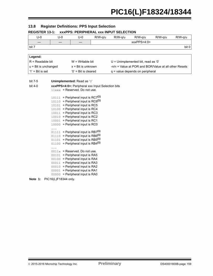
PIC16(L)F18324/18344
13.8 Register Definitions: PPS Input Selection
REGISTER 13-1: xxxPPS: PERIPHERAL xxx INPUT SELECTION
U-0 U-0 U-0 R/W-q/u R/W-q/u R/W-q/u R/W-q/u R/W-q/u
— — — xxxPPS<4:0>
bit 7 bit 0
Legend:
R = Readable bit W = Writable bit U = Unimplemented bit, read as ‘0’
u = Bit is unchanged x = Bit is unknown -n/n = Value at POR and BOR/Value at all other Resets
‘1’ = Bit is set ‘0’ = Bit is cleared q = value depends on peripheral
bit 7-5 Unimplemented: Read as ‘0’
bit 4-0 xxxPPS<4:0>: Peripheral xxx Input Selection bits11xxx = Reserved. Do not use.
10111 = Peripheral input is RC7(1)
10110 = Peripheral input is RC6(1)
10101 = Peripheral input is RC510100 = Peripheral input is RC410011 = Peripheral input is RC310010 = Peripheral input is RC210001 = Peripheral input is RC110000 = Peripheral input is RC0...01111 = Peripheral input is RB7(1)
01110 = Peripheral input is RB6(1)
01101 = Peripheral input is RB5(1)
01100 = Peripheral input is RB4(1)
...0011x = Reserved. Do not use.00101 = Peripheral input is RA500100 = Peripheral input is RA400011 = Peripheral input is RA300010 = Peripheral input is RA200001 = Peripheral input is RA100000 = Peripheral input is RA0
Note 1: PIC16(L)F18344 only.
2015-2016 Microchip Technology Inc. Preliminary DS40001800B-page 159
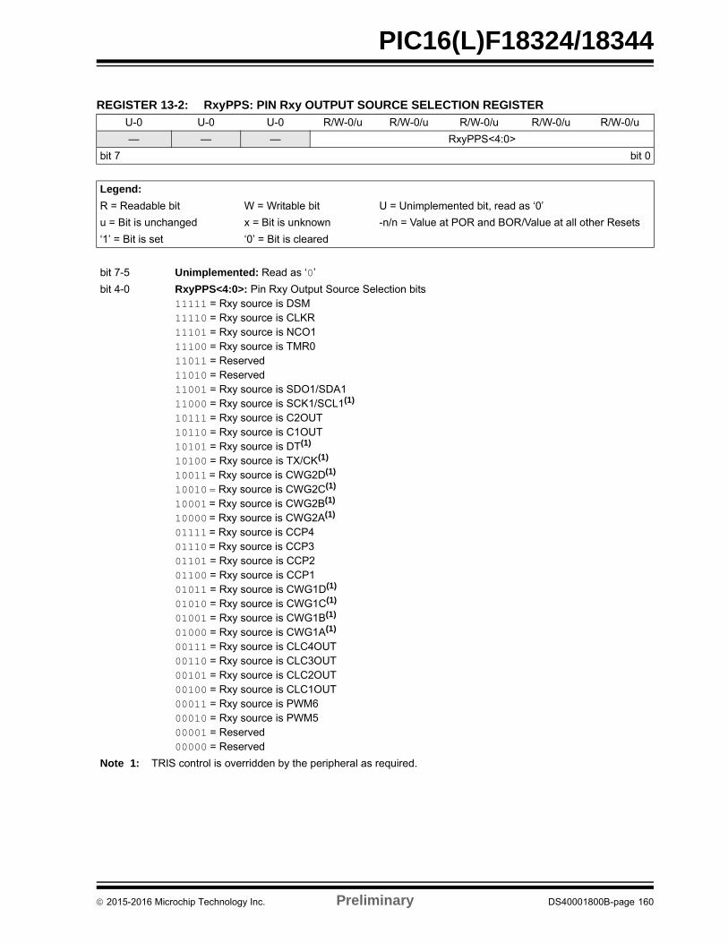
PIC16(L)F18324/18344
REGISTER 13-2: RxyPPS: PIN Rxy OUTPUT SOURCE SELECTION REGISTER
U-0 U-0 U-0 R/W-0/u R/W-0/u R/W-0/u R/W-0/u R/W-0/u
— — — RxyPPS<4:0>
bit 7 bit 0
Legend:
R = Readable bit W = Writable bit U = Unimplemented bit, read as ‘0’
u = Bit is unchanged x = Bit is unknown -n/n = Value at POR and BOR/Value at all other Resets
‘1’ = Bit is set ‘0’ = Bit is cleared
bit 7-5 Unimplemented: Read as ‘0’
bit 4-0 RxyPPS<4:0>: Pin Rxy Output Source Selection bits11111 = Rxy source is DSM11110 = Rxy source is CLKR11101 = Rxy source is NCO111100 = Rxy source is TMR011011 = Reserved11010 = Reserved11001 = Rxy source is SDO1/SDA111000 = Rxy source is SCK1/SCL1(1)
10111 = Rxy source is C2OUT10110 = Rxy source is C1OUT10101 = Rxy source is DT(1)
10100 = Rxy source is TX/CK(1)
10011 = Rxy source is CWG2D(1)
10010 = Rxy source is CWG2C(1)
10001 = Rxy source is CWG2B(1)
10000 = Rxy source is CWG2A(1)
01111 = Rxy source is CCP401110 = Rxy source is CCP301101 = Rxy source is CCP201100 = Rxy source is CCP101011 = Rxy source is CWG1D(1)
01010 = Rxy source is CWG1C(1)
01001 = Rxy source is CWG1B(1)
01000 = Rxy source is CWG1A(1)
00111 = Rxy source is CLC4OUT 00110 = Rxy source is CLC3OUT00101 = Rxy source is CLC2OUT00100 = Rxy source is CLC1OUT00011 = Rxy source is PWM600010 = Rxy source is PWM500001 = Reserved00000 = Reserved
Note 1: TRIS control is overridden by the peripheral as required.
2015-2016 Microchip Technology Inc. Preliminary DS40001800B-page 160
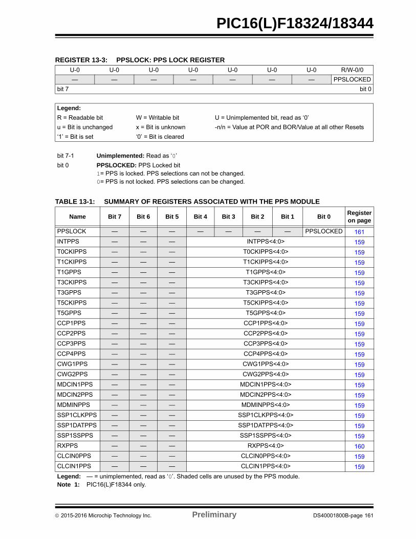
PIC16(L)F18324/18344
REGISTER 13-3: PPSLOCK: PPS LOCK REGISTER
U-0 U-0 U-0 U-0 U-0 U-0 U-0 R/W-0/0
— — — — — — — PPSLOCKED
bit 7 bit 0
Legend:
R = Readable bit W = Writable bit U = Unimplemented bit, read as ‘0’
u = Bit is unchanged x = Bit is unknown -n/n = Value at POR and BOR/Value at all other Resets
‘1’ = Bit is set ‘0’ = Bit is cleared
bit 7-1 Unimplemented: Read as ‘0’
bit 0 PPSLOCKED: PPS Locked bit1= PPS is locked. PPS selections can not be changed.0= PPS is not locked. PPS selections can be changed.
TABLE 13-1: SUMMARY OF REGISTERS ASSOCIATED WITH THE PPS MODULE
Name Bit 7 Bit 6 Bit 5 Bit 4 Bit 3 Bit 2 Bit 1 Bit 0Register on page
PPSLOCK — — — — — — — PPSLOCKED 161
INTPPS — — — INTPPS<4:0> 159
T0CKIPPS — — — T0CKIPPS<4:0> 159
T1CKIPPS — — — T1CKIPPS<4:0> 159
T1GPPS — — — T1GPPS<4:0> 159
T3CKIPPS — — — T3CKIPPS<4:0> 159
T3GPPS — — — T3GPPS<4:0> 159
T5CKIPPS — — — T5CKIPPS<4:0> 159
T5GPPS — — — T5GPPS<4:0> 159
CCP1PPS — — — CCP1PPS<4:0> 159
CCP2PPS — — — CCP2PPS<4:0> 159
CCP3PPS — — — CCP3PPS<4:0> 159
CCP4PPS — — — CCP4PPS<4:0> 159
CWG1PPS — — — CWG1PPS<4:0> 159
CWG2PPS — — — CWG2PPS<4:0> 159
MDCIN1PPS — — — MDCIN1PPS<4:0> 159
MDCIN2PPS — — — MDCIN2PPS<4:0> 159
MDMINPPS — — — MDMINPPS<4:0> 159
SSP1CLKPPS — — — SSP1CLKPPS<4:0> 159
SSP1DATPPS — — — SSP1DATPPS<4:0> 159
SSP1SSPPS — — — SSP1SSPPS<4:0> 159
RXPPS — — — RXPPS<4:0> 160
CLCIN0PPS — — — CLCIN0PPS<4:0> 159
CLCIN1PPS — — — CLCIN1PPS<4:0> 159
Legend: — = unimplemented, read as ‘0’. Shaded cells are unused by the PPS module.Note 1: PIC16(L)F18344 only.
2015-2016 Microchip Technology Inc. Preliminary DS40001800B-page 161
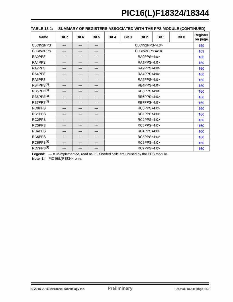
PIC16(L)F18324/18344
CLCIN2PPS — — — CLCIN2PPS<4:0> 159
CLCIN3PPS — — — CLCIN3PPS<4:0> 159
RA0PPS — — — RA0PPS<4:0> 160
RA1PPS — — — RA1PPS<4:0> 160
RA2PPS — — — RA2PPS<4:0> 160
RA4PPS — — — RA4PPS<4:0> 160
RA5PPS — — — RA5PPS<4:0> 160
RB4PPS(1) — — — RB4PPS<4:0> 160
RB5PPS(1) — — — RB5PPS<4:0> 160
RB6PPS(1) — — — RB6PPS<4:0> 160
RB7PPS(1) — — — RB7PPS<4:0> 160
RC0PPS — — — RC0PPS<4:0> 160
RC1PPS — — — RC1PPS<4:0> 160
RC2PPS — — — RC2PPS<4:0> 160
RC3PPS — — — RC3PPS<4:0> 160
RC4PPS — — — RC4PPS<4:0> 160
RC5PPS — — — RC5PPS<4:0> 160
RC6PPS(1) — — — RC6PPS<4:0> 160
RC7PPS(1) — — — RC7PPS<4:0> 160
TABLE 13-1: SUMMARY OF REGISTERS ASSOCIATED WITH THE PPS MODULE (CONTINUED)
Name Bit 7 Bit 6 Bit 5 Bit 4 Bit 3 Bit 2 Bit 1 Bit 0Register on page
Legend: — = unimplemented, read as ‘0’. Shaded cells are unused by the PPS module.Note 1: PIC16(L)F18344 only.
2015-2016 Microchip Technology Inc. Preliminary DS40001800B-page 162
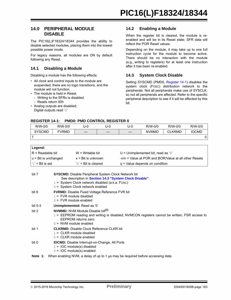
PIC16(L)F18324/18344
14.0 PERIPHERAL MODULE DISABLE
The PIC16(L)F18324/18344 provides the ability todisable selected modules, placing them into the lowestpossible power mode.
For legacy reasons, all modules are ON by defaultfollowing any Reset.
14.1 Disabling a Module
Disabling a module has the following effects:
• All clock and control inputs to the module are suspended; there are no logic transitions, and the module will not function.
• The module is held in Reset.- Writing to the SFRs is disabled- Reads return 00h
• Analog outputs are disabled;Digital outputs read ‘0’
14.2 Enabling a Module
When the register bit is cleared, the module is re-enabled and will be in its Reset state; SFR data willreflect the POR Reset values.
Depending on the module, it may take up to one fullinstruction cycle for the module to become active.There should be no interaction with the module(e.g., writing to registers) for at least one instructionafter it has been re-enabled.
14.3 System Clock Disable
Setting SYSCMD (PMD0, Register 14-1) disables thesystem clock (FOSC) distribution network to theperipherals. Not all peripherals make use of SYSCLK,so not all peripherals are affected. Refer to the specificperipheral description to see if it will be affected by thisbit.
REGISTER 14-1: PMD0: PMD CONTROL REGISTER 0
R/W-0/0 R/W-0/0 U-0 U-0 U-0 R/W-0/0 R/W-0/0 R/W-0/0
SYSCMD FVRMD — — — NVMMD CLKRMD IOCMD
7 0
Legend:
R = Readable bit W = Writable bit U = Unimplemented bit, read as ‘0’
u = Bit is unchanged x = Bit is unknown -n/n = Value at POR and BOR/Value at all other Resets
‘1’ = Bit is set ‘0’ = Bit is cleared q = Value depends on condition
bit 7 SYSCMD: Disable Peripheral System Clock Network bitSee description in Section 14.3 “System Clock Disable”.
1 = System Clock network disabled (a.k.a. FOSC)0 = System Clock network enabled
bit 6 FVRMD: Disable Fixed Voltage Reference FVR bit1 = FVR module disabled0 = FVR module enabled
bit 5-3 Unimplemented: Read as ‘0’
bit 2 NVMMD: NVM Module Disable bit(1)
1 = EEPROM reading and writing is disabled; NVMCON registers cannot be written; FSR access toEEPROM returns zero.
0 = NVM module enabled
bit 1 CLKRMD: Disable Clock Reference CLKR bit1 = CLKR module disabled0 = CLKR module enabled
bit 0 IOCMD: Disable Interrupt-on-Change, All Ports1 = IOC module(s) disabled0 = IOC module(s) enabled
Note 1: When enabling NVM, a delay of up to 1 µs may be required before accessing data.
2015-2016 Microchip Technology Inc. Preliminary DS40001800B-page 163
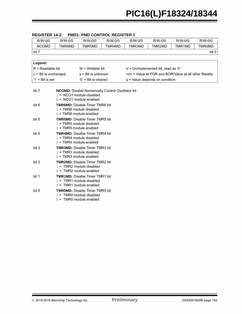
PIC16(L)F18324/18344
REGISTER 14-2: PMD1: PMD CONTROL REGISTER 1
R/W-0/0 R/W-0/0 R/W-0/0 R/W-0/0 R/W-0/0 R/W-0/0 R/W-0/0 R/W-0/0
NCOMD TMR6MD TMR5MD TMR4MD TMR3MD TMR2MD TMR1MD TMR0MD
bit 7 bit 0
Legend:
R = Readable bit W = Writable bit U = Unimplemented bit, read as ‘0’
u = Bit is unchanged x = Bit is unknown -n/n = Value at POR and BOR/Value at all other Resets
‘1’ = Bit is set ‘0’ = Bit is cleared q = Value depends on condition
bit 7 NCOMD: Disable Numerically Control Oscillator bit1 = NCO1 module disabled0 = NCO1 module enabled
bit 6 TMR6MD: Disable Timer TMR6 bit1 = TMR6 module disabled0 = TMR6 module enabled
bit 5 TMR5MD: Disable Timer TMR5 bit1 = TMR5 module disabled0 = TMR5 module enabled
bit 4 TMR4MD: Disable Timer TMR4 bit1 = TMR4 module disabled0 = TMR4 module enabled
bit 3 TMR3MD: Disable Timer TMR3 bit1 = TMR3 module disabled0 = TMR3 module enabled
bit 2 TMR2MD: Disable Timer TMR2 bit1 = TMR2 module disabled0 = TMR2 module enabled
bit 1 TMR1MD: Disable Timer TMR1 bit1 = TMR1 module disabled0 = TMR1 module enabled
bit 0 TMR0MD: Disable Timer TMR0 bit1 = TMR0 module disabled0 = TMR0 module enabled
2015-2016 Microchip Technology Inc. Preliminary DS40001800B-page 164
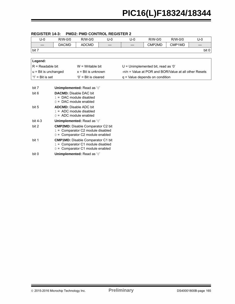
PIC16(L)F18324/18344
REGISTER 14-3: PMD2: PMD CONTROL REGISTER 2
U-0 R/W-0/0 R/W-0/0 U-0 U-0 R/W-0/0 R/W-0/0 U-0
— DACMD ADCMD — — CMP2MD CMP1MD —
bit 7 bit 0
Legend:
R = Readable bit W = Writable bit U = Unimplemented bit, read as ‘0’
u = Bit is unchanged x = Bit is unknown -n/n = Value at POR and BOR/Value at all other Resets
‘1’ = Bit is set ‘0’ = Bit is cleared q = Value depends on condition
bit 7 Unimplemented: Read as ‘0’
bit 6 DACMD: Disable DAC bit1 = DAC module disabled0 = DAC module enabled
bit 5 ADCMD: Disable ADC bit1 = ADC module disabled0 = ADC module enabled
bit 4-3 Unimplemented: Read as ‘0’
bit 2 CMP2MD: Disable Comparator C2 bit1 = Comparator C2 module disabled0 = Comparator C2 module enabled
bit 1 CMP1MD: Disable Comparator C1 bit1 = Comparator C1 module disabled0 = Comparator C1 module enabled
bit 0 Unimplemented: Read as ‘0’
2015-2016 Microchip Technology Inc. Preliminary DS40001800B-page 165
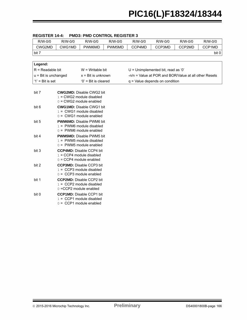
PIC16(L)F18324/18344
REGISTER 14-4: PMD3: PMD CONTROL REGISTER 3
R/W-0/0 R/W-0/0 R/W-0/0 R/W-0/0 R/W-0/0 R/W-0/0 R/W-0/0 R/W-0/0
CWG2MD CWG1MD PWM6MD PWM5MD CCP4MD CCP3MD CCP2MD CCP1MD
bit 7 bit 0
Legend:
R = Readable bit W = Writable bit U = Unimplemented bit, read as ‘0’
u = Bit is unchanged x = Bit is unknown -n/n = Value at POR and BOR/Value at all other Resets
‘1’ = Bit is set ‘0’ = Bit is cleared q = Value depends on condition
bit 7 CWG2MD: Disable CWG2 bit1 = CWG2 module disabled0 = CWG2 module enabled
bit 6 CWG1MD: Disable CWG1 bit1 = CWG1 module disabled0 = CWG1 module enabled
bit 5 PWM6MD: Disable PWM6 bit1 = PWM6 module disabled0 = PWM6 module enabled
bit 4 PWM5MD: Disable PWM5 bit1 = PWM5 module disabled0 = PWM5 module enabled
bit 3 CCP4MD: Disable CCP4 bit1 = CCP4 module disabled0 = CCP4 module enabled
bit 2 CCP3MD: Disable CCP3 bit1 = CCP3 module disabled0 = CCP3 module enabled
bit 1 CCP2MD: Disable CCP2 bit1 = CCP2 module disabled0 =CCP2 module enabled
bit 0 CCP1MD: Disable CCP1 bit1 = CCP1 module disabled0 = CCP1 module enabled
2015-2016 Microchip Technology Inc. Preliminary DS40001800B-page 166
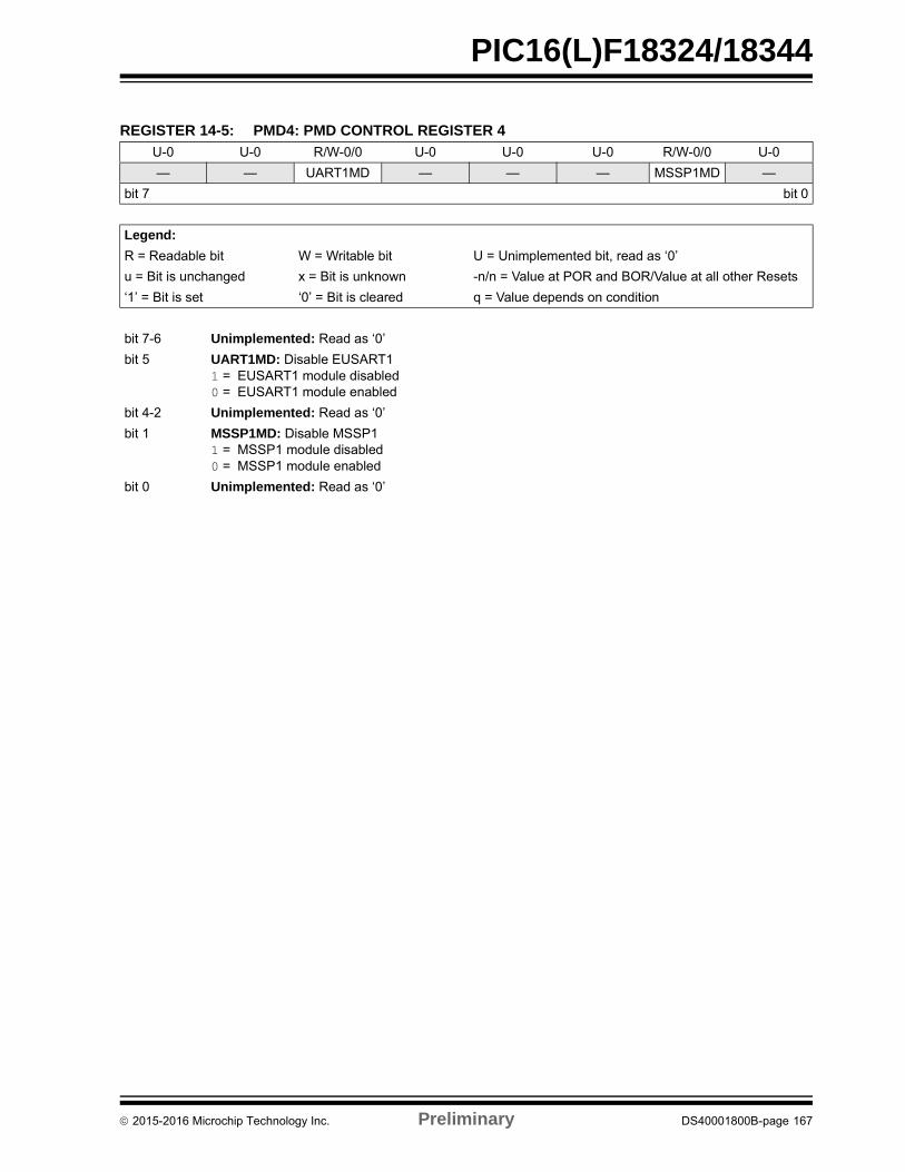
PIC16(L)F18324/18344
REGISTER 14-5: PMD4: PMD CONTROL REGISTER 4
U-0 U-0 R/W-0/0 U-0 U-0 U-0 R/W-0/0 U-0
— — UART1MD — — — MSSP1MD —
bit 7 bit 0
Legend:
R = Readable bit W = Writable bit U = Unimplemented bit, read as ‘0’
u = Bit is unchanged x = Bit is unknown -n/n = Value at POR and BOR/Value at all other Resets
‘1’ = Bit is set ‘0’ = Bit is cleared q = Value depends on condition
bit 7-6 Unimplemented: Read as ‘0’
bit 5 UART1MD: Disable EUSART11 = EUSART1 module disabled0 = EUSART1 module enabled
bit 4-2 Unimplemented: Read as ‘0’
bit 1 MSSP1MD: Disable MSSP11 = MSSP1 module disabled0 = MSSP1 module enabled
bit 0 Unimplemented: Read as ‘0’
2015-2016 Microchip Technology Inc. Preliminary DS40001800B-page 167
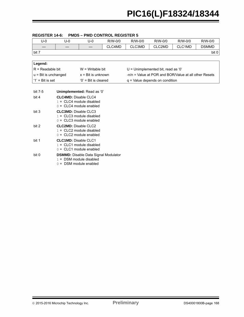
PIC16(L)F18324/18344
REGISTER 14-6: PMD5 – PMD CONTROL REGISTER 5
U-0 U-0 U-0 R/W-0/0 R/W-0/0 R/W-0/0 R/W-0/0 R/W-0/0
— — — CLC4MD CLC3MD CLC2MD CLC1MD DSMMD
bit 7 bit 0
Legend:
R = Readable bit W = Writable bit U = Unimplemented bit, read as ‘0’
u = Bit is unchanged x = Bit is unknown -n/n = Value at POR and BOR/Value at all other Resets
‘1’ = Bit is set ‘0’ = Bit is cleared q = Value depends on condition
bit 7-5 Unimplemented: Read as ‘0’
bit 4 CLC4MD: Disable CLC41 = CLC4 module disabled0 = CLC4 module enabled
bit 3 CLC3MD: Disable CLC31 = CLC3 module disabled0 = CLC3 module enabled
bit 2 CLC2MD: Disable CLC21 = CLC2 module disabled0 = CLC2 module enabled
bit 1 CLC1MD: Disable CLC11 = CLC1 module disabled0 = CLC1 module enabled
bit 0 DSMMD: Disable Data Signal Modulator1 = DSM module disabled0 = DSM module enabled
2015-2016 Microchip Technology Inc. Preliminary DS40001800B-page 168
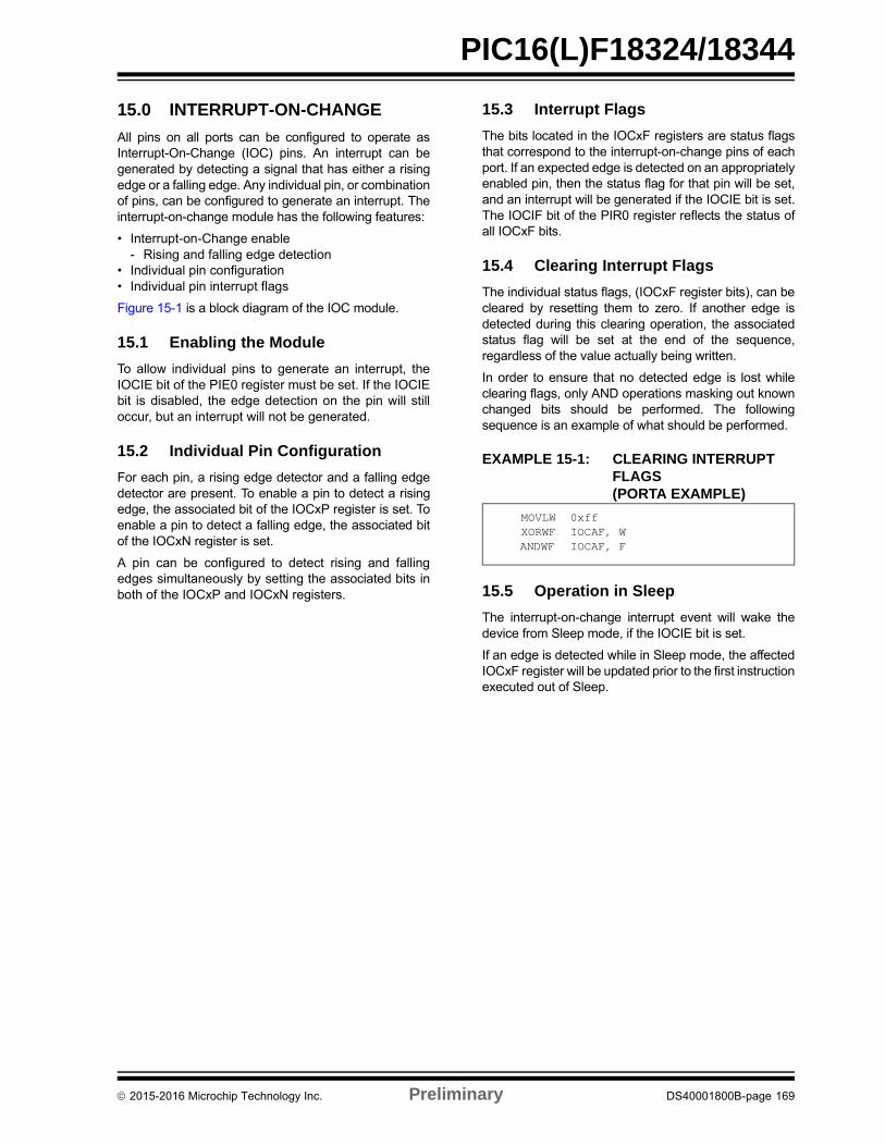
PIC16(L)F18324/18344
15.0 INTERRUPT-ON-CHANGE
All pins on all ports can be configured to operate asInterrupt-On-Change (IOC) pins. An interrupt can begenerated by detecting a signal that has either a risingedge or a falling edge. Any individual pin, or combinationof pins, can be configured to generate an interrupt. Theinterrupt-on-change module has the following features:
• Interrupt-on-Change enable- Rising and falling edge detection
• Individual pin configuration• Individual pin interrupt flags
Figure 15-1 is a block diagram of the IOC module.
15.1 Enabling the Module
To allow individual pins to generate an interrupt, theIOCIE bit of the PIE0 register must be set. If the IOCIEbit is disabled, the edge detection on the pin will stilloccur, but an interrupt will not be generated.
15.2 Individual Pin Configuration
For each pin, a rising edge detector and a falling edgedetector are present. To enable a pin to detect a risingedge, the associated bit of the IOCxP register is set. Toenable a pin to detect a falling edge, the associated bitof the IOCxN register is set.
A pin can be configured to detect rising and fallingedges simultaneously by setting the associated bits inboth of the IOCxP and IOCxN registers.
15.3 Interrupt Flags
The bits located in the IOCxF registers are status flagsthat correspond to the interrupt-on-change pins of eachport. If an expected edge is detected on an appropriatelyenabled pin, then the status flag for that pin will be set,and an interrupt will be generated if the IOCIE bit is set.The IOCIF bit of the PIR0 register reflects the status ofall IOCxF bits.
15.4 Clearing Interrupt Flags
The individual status flags, (IOCxF register bits), can becleared by resetting them to zero. If another edge isdetected during this clearing operation, the associatedstatus flag will be set at the end of the sequence,regardless of the value actually being written.
In order to ensure that no detected edge is lost whileclearing flags, only AND operations masking out knownchanged bits should be performed. The followingsequence is an example of what should be performed.
EXAMPLE 15-1: CLEARING INTERRUPT FLAGS(PORTA EXAMPLE)
15.5 Operation in Sleep
The interrupt-on-change interrupt event will wake thedevice from Sleep mode, if the IOCIE bit is set.
If an edge is detected while in Sleep mode, the affectedIOCxF register will be updated prior to the first instructionexecuted out of Sleep.
MOVLW 0xffXORWF IOCAF, WANDWF IOCAF, F
2015-2016 Microchip Technology Inc. Preliminary DS40001800B-page 169

PIC16(L)F18324/18344
FIGURE 15-1: INTERRUPT-ON-CHANGE BLOCK DIAGRAM (PORTA EXAMPLE)
IOCANx
IOCAPx
Q2
Q4Q1
data bus =0 or 1
write IOCAFx
IOCIE
to data busIOCAFx
edgedetect
IOC interruptto CPU core
from all other IOCnFx individual
pin detectors
D QS
D Q
R
D Q
R
RAx
Rev. 10-000037D10/3/2016
2015-2016 Microchip Technology Inc. Preliminary DS40001800B-page 170
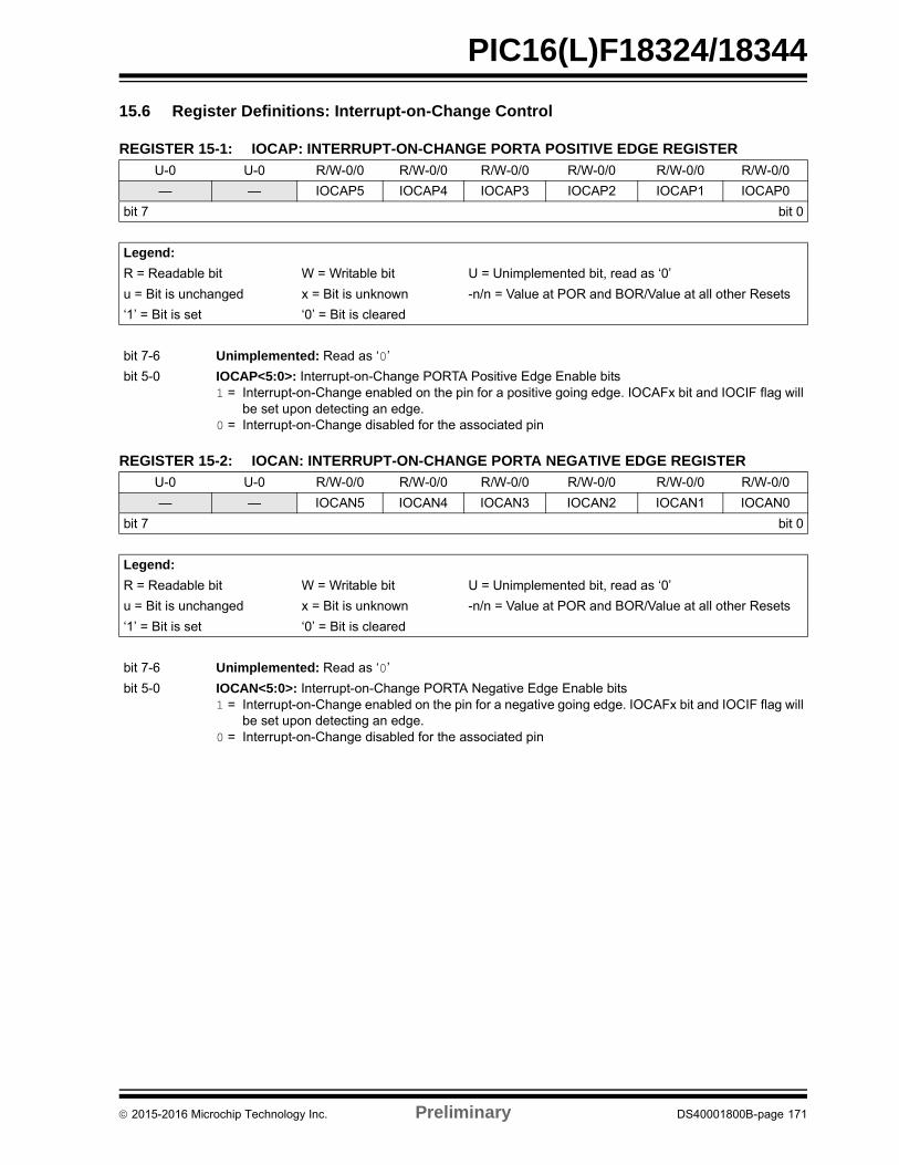
PIC16(L)F18324/18344
15.6 Register Definitions: Interrupt-on-Change Control
REGISTER 15-1: IOCAP: INTERRUPT-ON-CHANGE PORTA POSITIVE EDGE REGISTER
U-0 U-0 R/W-0/0 R/W-0/0 R/W-0/0 R/W-0/0 R/W-0/0 R/W-0/0
— — IOCAP5 IOCAP4 IOCAP3 IOCAP2 IOCAP1 IOCAP0
bit 7 bit 0
Legend:
R = Readable bit W = Writable bit U = Unimplemented bit, read as ‘0’
u = Bit is unchanged x = Bit is unknown -n/n = Value at POR and BOR/Value at all other Resets
‘1’ = Bit is set ‘0’ = Bit is cleared
bit 7-6 Unimplemented: Read as ‘0’
bit 5-0 IOCAP<5:0>: Interrupt-on-Change PORTA Positive Edge Enable bits1 = Interrupt-on-Change enabled on the pin for a positive going edge. IOCAFx bit and IOCIF flag will
be set upon detecting an edge.0 = Interrupt-on-Change disabled for the associated pin
REGISTER 15-2: IOCAN: INTERRUPT-ON-CHANGE PORTA NEGATIVE EDGE REGISTER
U-0 U-0 R/W-0/0 R/W-0/0 R/W-0/0 R/W-0/0 R/W-0/0 R/W-0/0
— — IOCAN5 IOCAN4 IOCAN3 IOCAN2 IOCAN1 IOCAN0
bit 7 bit 0
Legend:
R = Readable bit W = Writable bit U = Unimplemented bit, read as ‘0’
u = Bit is unchanged x = Bit is unknown -n/n = Value at POR and BOR/Value at all other Resets
‘1’ = Bit is set ‘0’ = Bit is cleared
bit 7-6 Unimplemented: Read as ‘0’
bit 5-0 IOCAN<5:0>: Interrupt-on-Change PORTA Negative Edge Enable bits1 = Interrupt-on-Change enabled on the pin for a negative going edge. IOCAFx bit and IOCIF flag will
be set upon detecting an edge.0 = Interrupt-on-Change disabled for the associated pin
2015-2016 Microchip Technology Inc. Preliminary DS40001800B-page 171
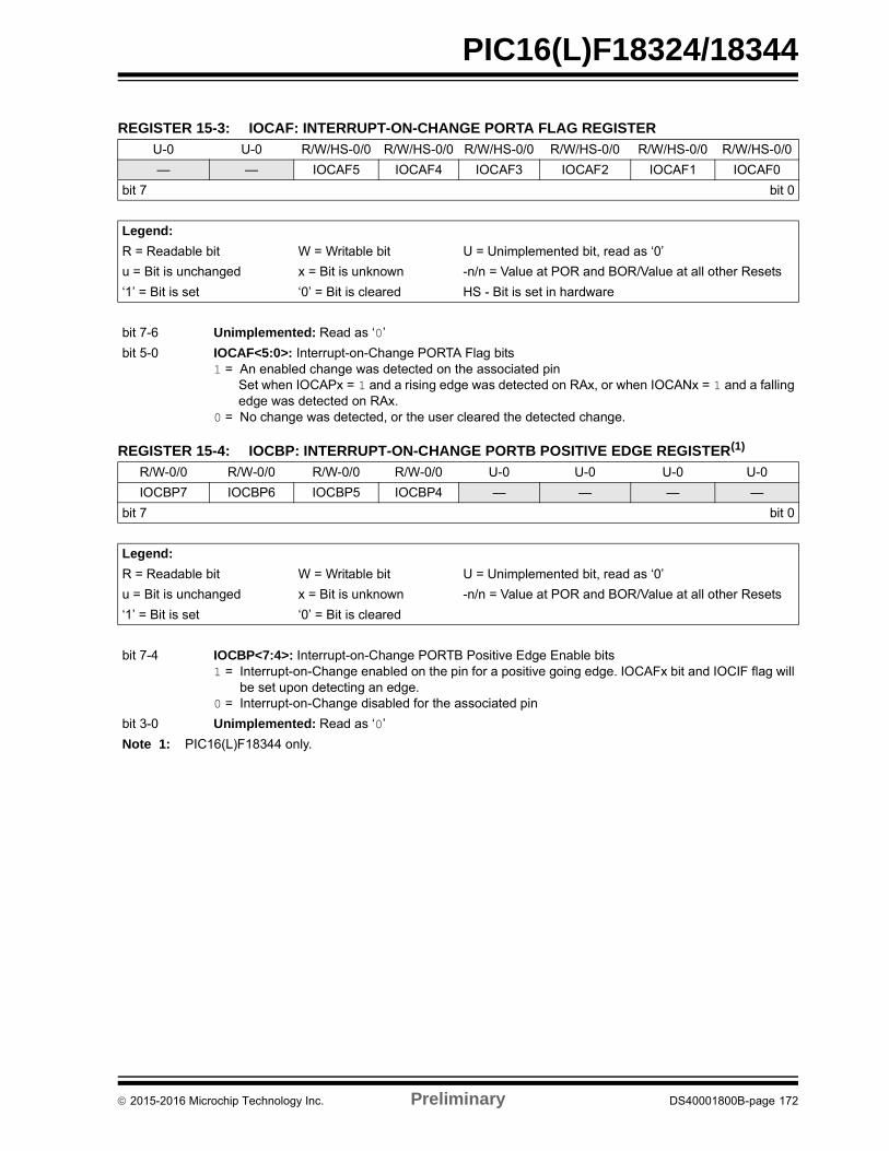
PIC16(L)F18324/18344
REGISTER 15-3: IOCAF: INTERRUPT-ON-CHANGE PORTA FLAG REGISTER
U-0 U-0 R/W/HS-0/0 R/W/HS-0/0 R/W/HS-0/0 R/W/HS-0/0 R/W/HS-0/0 R/W/HS-0/0
— — IOCAF5 IOCAF4 IOCAF3 IOCAF2 IOCAF1 IOCAF0
bit 7 bit 0
Legend:
R = Readable bit W = Writable bit U = Unimplemented bit, read as ‘0’
u = Bit is unchanged x = Bit is unknown -n/n = Value at POR and BOR/Value at all other Resets
‘1’ = Bit is set ‘0’ = Bit is cleared HS - Bit is set in hardware
bit 7-6 Unimplemented: Read as ‘0’
bit 5-0 IOCAF<5:0>: Interrupt-on-Change PORTA Flag bits1 = An enabled change was detected on the associated pin
Set when IOCAPx = 1 and a rising edge was detected on RAx, or when IOCANx = 1 and a fallingedge was detected on RAx.
0 = No change was detected, or the user cleared the detected change.
REGISTER 15-4: IOCBP: INTERRUPT-ON-CHANGE PORTB POSITIVE EDGE REGISTER(1)
R/W-0/0 R/W-0/0 R/W-0/0 R/W-0/0 U-0 U-0 U-0 U-0
IOCBP7 IOCBP6 IOCBP5 IOCBP4 — — — —
bit 7 bit 0
Legend:
R = Readable bit W = Writable bit U = Unimplemented bit, read as ‘0’
u = Bit is unchanged x = Bit is unknown -n/n = Value at POR and BOR/Value at all other Resets
‘1’ = Bit is set ‘0’ = Bit is cleared
bit 7-4 IOCBP<7:4>: Interrupt-on-Change PORTB Positive Edge Enable bits1 = Interrupt-on-Change enabled on the pin for a positive going edge. IOCAFx bit and IOCIF flag will
be set upon detecting an edge.0 = Interrupt-on-Change disabled for the associated pin
bit 3-0 Unimplemented: Read as ‘0’
Note 1: PIC16(L)F18344 only.
2015-2016 Microchip Technology Inc. Preliminary DS40001800B-page 172
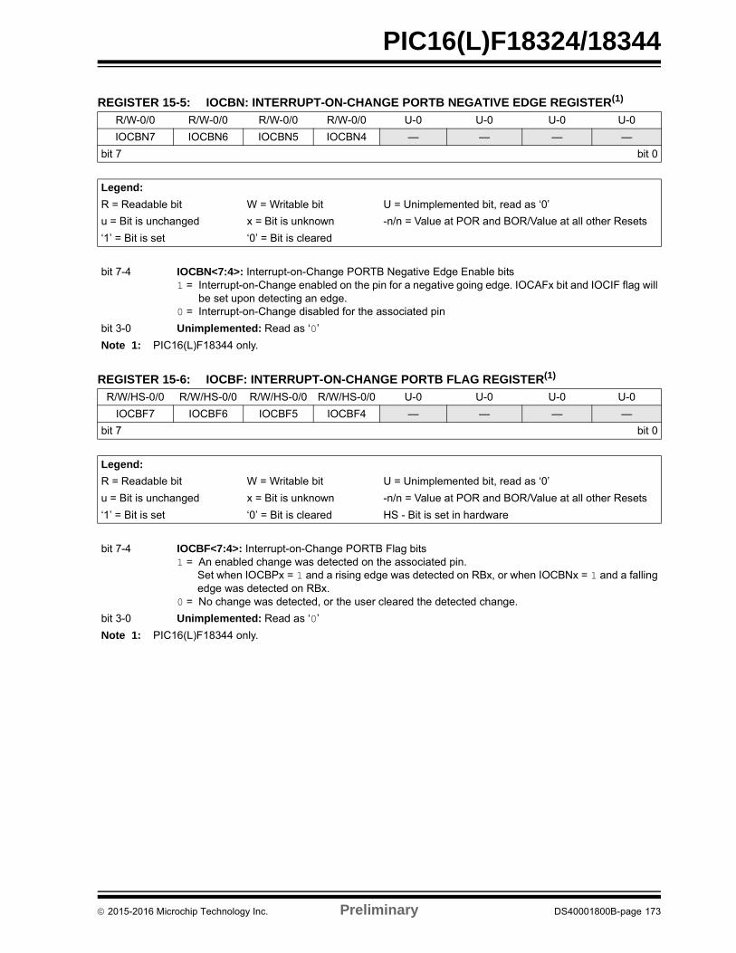
PIC16(L)F18324/18344
REGISTER 15-5: IOCBN: INTERRUPT-ON-CHANGE PORTB NEGATIVE EDGE REGISTER(1)
R/W-0/0 R/W-0/0 R/W-0/0 R/W-0/0 U-0 U-0 U-0 U-0
IOCBN7 IOCBN6 IOCBN5 IOCBN4 — — — —
bit 7 bit 0
Legend:
R = Readable bit W = Writable bit U = Unimplemented bit, read as ‘0’
u = Bit is unchanged x = Bit is unknown -n/n = Value at POR and BOR/Value at all other Resets
‘1’ = Bit is set ‘0’ = Bit is cleared
bit 7-4 IOCBN<7:4>: Interrupt-on-Change PORTB Negative Edge Enable bits1 = Interrupt-on-Change enabled on the pin for a negative going edge. IOCAFx bit and IOCIF flag will
be set upon detecting an edge.0 = Interrupt-on-Change disabled for the associated pin
bit 3-0 Unimplemented: Read as ‘0’
Note 1: PIC16(L)F18344 only.
REGISTER 15-6: IOCBF: INTERRUPT-ON-CHANGE PORTB FLAG REGISTER(1)
R/W/HS-0/0 R/W/HS-0/0 R/W/HS-0/0 R/W/HS-0/0 U-0 U-0 U-0 U-0
IOCBF7 IOCBF6 IOCBF5 IOCBF4 — — — —
bit 7 bit 0
Legend:
R = Readable bit W = Writable bit U = Unimplemented bit, read as ‘0’
u = Bit is unchanged x = Bit is unknown -n/n = Value at POR and BOR/Value at all other Resets
‘1’ = Bit is set ‘0’ = Bit is cleared HS - Bit is set in hardware
bit 7-4 IOCBF<7:4>: Interrupt-on-Change PORTB Flag bits1 = An enabled change was detected on the associated pin.
Set when IOCBPx = 1 and a rising edge was detected on RBx, or when IOCBNx = 1 and a fallingedge was detected on RBx.
0 = No change was detected, or the user cleared the detected change.
bit 3-0 Unimplemented: Read as ‘0’
Note 1: PIC16(L)F18344 only.
2015-2016 Microchip Technology Inc. Preliminary DS40001800B-page 173
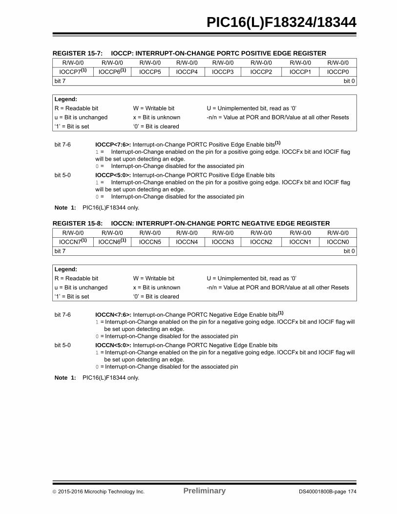
PIC16(L)F18324/18344
REGISTER 15-7: IOCCP: INTERRUPT-ON-CHANGE PORTC POSITIVE EDGE REGISTER
R/W-0/0 R/W-0/0 R/W-0/0 R/W-0/0 R/W-0/0 R/W-0/0 R/W-0/0 R/W-0/0
IOCCP7(1) IOCCP6(1) IOCCP5 IOCCP4 IOCCP3 IOCCP2 IOCCP1 IOCCP0
bit 7 bit 0
Legend:
R = Readable bit W = Writable bit U = Unimplemented bit, read as ‘0’
u = Bit is unchanged x = Bit is unknown -n/n = Value at POR and BOR/Value at all other Resets
‘1’ = Bit is set ‘0’ = Bit is cleared
bit 7-6 IOCCP<7:6>: Interrupt-on-Change PORTC Positive Edge Enable bits(1)
1 = Interrupt-on-Change enabled on the pin for a positive going edge. IOCCFx bit and IOCIF flag will be set upon detecting an edge.0 = Interrupt-on-Change disabled for the associated pin
bit 5-0 IOCCP<5:0>: Interrupt-on-Change PORTC Positive Edge Enable bits1 = Interrupt-on-Change enabled on the pin for a positive going edge. IOCCFx bit and IOCIF flag will be set upon detecting an edge.0 = Interrupt-on-Change disabled for the associated pin
Note 1: PIC16(L)F18344 only.
REGISTER 15-8: IOCCN: INTERRUPT-ON-CHANGE PORTC NEGATIVE EDGE REGISTER
R/W-0/0 R/W-0/0 R/W-0/0 R/W-0/0 R/W-0/0 R/W-0/0 R/W-0/0 R/W-0/0
IOCCN7(1) IOCCN6(1) IOCCN5 IOCCN4 IOCCN3 IOCCN2 IOCCN1 IOCCN0
bit 7 bit 0
Legend:
R = Readable bit W = Writable bit U = Unimplemented bit, read as ‘0’
u = Bit is unchanged x = Bit is unknown -n/n = Value at POR and BOR/Value at all other Resets
‘1’ = Bit is set ‘0’ = Bit is cleared
bit 7-6 IOCCN<7:6>: Interrupt-on-Change PORTC Negative Edge Enable bits(1)
1 = Interrupt-on-Change enabled on the pin for a negative going edge. IOCCFx bit and IOCIF flag willbe set upon detecting an edge.
0 = Interrupt-on-Change disabled for the associated pin
bit 5-0 IOCCN<5:0>: Interrupt-on-Change PORTC Negative Edge Enable bits1 = Interrupt-on-Change enabled on the pin for a negative going edge. IOCCFx bit and IOCIF flag will
be set upon detecting an edge.0 = Interrupt-on-Change disabled for the associated pin
Note 1: PIC16(L)F18344 only.
2015-2016 Microchip Technology Inc. Preliminary DS40001800B-page 174
PIC16(L)F18324/18344
REGISTER 15-9: IOCCF: INTERRUPT-ON-CHANGE PORTC FLAG REGISTER
R/W/HS-0/0 R/W/HS-0/0 R/W/HS-0/0 R/W/HS-0/0 R/W/HS-0/0 R/W/HS-0/0 R/W/HS-0/0 R/W/HS-0/0
IOCCF7(1) IOCCF6(1) IOCCF5 IOCCF4 IOCCF3 IOCCF2 IOCCF1 IOCCF0
bit 7 bit 0
Legend:
R = Readable bit W = Writable bit U = Unimplemented bit, read as ‘0’
u = Bit is unchanged x = Bit is unknown -n/n = Value at POR and BOR/Value at all other Resets
‘1’ = Bit is set ‘0’ = Bit is cleared HS - Bit is set in hardware
bit 7-6 IOCCF<7:6>: Interrupt-on-Change PORTC Flag bits1 = An enabled change was detected on the associated pin.
Set when IOCCPx = 1 and a rising edge was detected on RCx, or when IOCCNx = 1 and afalling edge was detected on RCx.
0 = No change was detected, or the user cleared the detected change.
bit 5-0 IOCCF<5:0>: Interrupt-on-Change PORTC Flag bits1 = An enabled change was detected on the associated pin.
Set when IOCCPx = 1 and a rising edge was detected on RCx, or when IOCCNx = 1 and afalling edge was detected on RCx.
0 = No change was detected, or the user cleared the detected change.
Note 1: PIC16(L)F18344 only.
TABLE 15-1: SUMMARY OF REGISTERS ASSOCIATED WITH INTERRUPT-ON-CHANGE
Name Bit 7 Bit 6 Bit 5 Bit 4 Bit 3 Bit 2 Bit 1 Bit 0Register on Page
ANSELA — — ANSA5 ANSA4 — ANSA2 ANSA1 ANSA0 141
ANSELB(1) ANSB7 ANSB6 ANSB5 ANSB4 — — — — 147
ANSELC ANSC7(1) ANSC6(1) ANSC5 ANSC4 ANSC3 ANSC2 ANSC1 ANSC0 154
TRISA — — TRISA5 TRISA4 —(2) TRISA2 TRISA1 TRISA0 140
TRISB(1) TRISB7 TRISB6 TRISB5 TRISB4 — — — — 146
TRISC TRISC7(1) TRISC6(1) TRISC5 TRISC4 TRISC3 TRISC2 TRISC1 TRISC0 153
INTCON GIE PEIE — — — — — INTEDG 98
PIE0 — — TMR0IE IOCIE — — — INTE 99
IOCAP — — IOCAP5 IOCAP4 IOCAP3 IOCAP2 IOCAP1 IOCAP0 171
IOCAN — — IOCAN5 IOCAN4 IOCAN3 IOCAN2 IOCAN1 IOCAN0 171
IOCAF — — IOCAF5 IOCAF4 IOCAF3 IOCAF2 IOCAF1 IOCAF0 172
IOCBP(1) IOCBP7 IOCBP6 IOCBP5 IOCBP4 — — — — 172
IOCBN(1) IOCBN7 IOCBN6 IOCBN5 IOCBN4 — — — — 173
IOCBF(1) IOCBF7 IOCBF6 IOCBF5 IOCBF4 — — — — 173
IOCCP IOCCP7(1) IOCCP6(1) IOCCP5 IOCCP4 IOCCP3 IOCCP2 IOCCP1 IOCCP0 174
IOCCN IOCCN7(1) IOCCN6(1) IOCCN5 IOCCN4 IOCCN3 IOCCN2 IOCCN1 IOCCN0 174
IOCCF IOCCF7(1) IOCCF6(1) IOCCF5 IOCCF4 IOCCF3 IOCCF2 IOCCF1 IOCCF0 175
Legend: — = unimplemented location, read as ‘0’. Shaded cells are not used by interrupt-on-change.
Note 1: PIC16(L)F18344 only.
2: Unimplemented, read as ‘1’.
2015-2016 Microchip Technology Inc. Preliminary DS40001800B-page 175
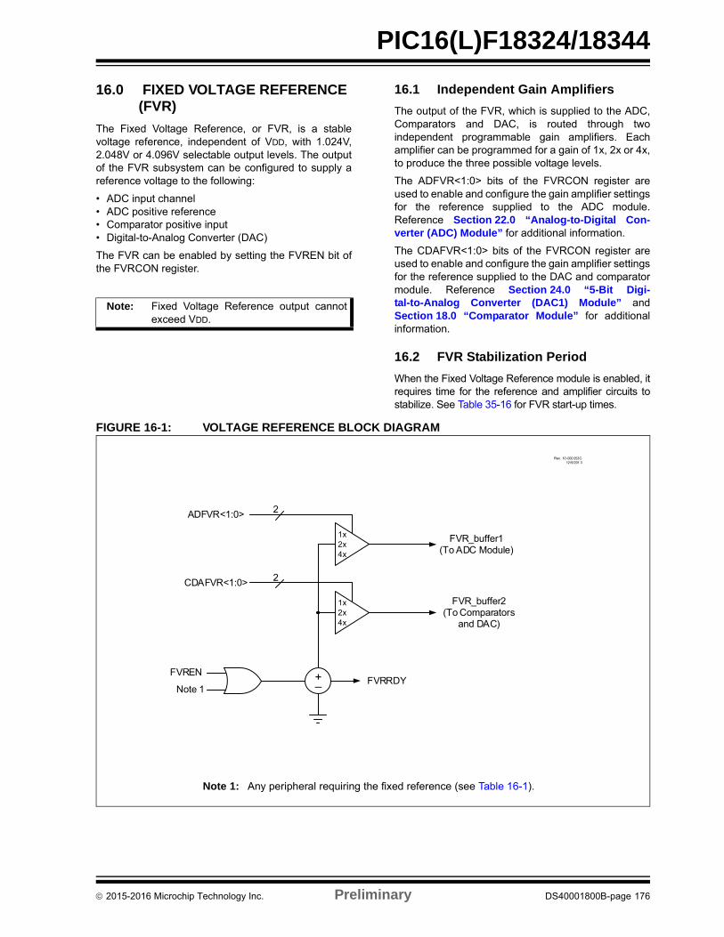
PIC16(L)F18324/18344
16.0 FIXED VOLTAGE REFERENCE (FVR)
The Fixed Voltage Reference, or FVR, is a stablevoltage reference, independent of VDD, with 1.024V,2.048V or 4.096V selectable output levels. The outputof the FVR subsystem can be configured to supply areference voltage to the following:
• ADC input channel• ADC positive reference• Comparator positive input• Digital-to-Analog Converter (DAC)
The FVR can be enabled by setting the FVREN bit ofthe FVRCON register.
16.1 Independent Gain Amplifiers
The output of the FVR, which is supplied to the ADC,Comparators and DAC, is routed through twoindependent programmable gain amplifiers. Eachamplifier can be programmed for a gain of 1x, 2x or 4x,to produce the three possible voltage levels.
The ADFVR<1:0> bits of the FVRCON register areused to enable and configure the gain amplifier settingsfor the reference supplied to the ADC module.Reference Section 22.0 “Analog-to-Digital Con-verter (ADC) Module” for additional information.
The CDAFVR<1:0> bits of the FVRCON register areused to enable and configure the gain amplifier settingsfor the reference supplied to the DAC and comparatormodule. Reference Section 24.0 “5-Bit Digi-tal-to-Analog Converter (DAC1) Module” andSection 18.0 “Comparator Module” for additionalinformation.
16.2 FVR Stabilization Period
When the Fixed Voltage Reference module is enabled, itrequires time for the reference and amplifier circuits tostabilize. See Table 35-16 for FVR start-up times.
FIGURE 16-1: VOLTAGE REFERENCE BLOCK DIAGRAM
Note: Fixed Voltage Reference output cannotexceed VDD.
Note 1: Any peripheral requiring the fixed reference (see Table 16-1).
1x 2x4x
1x 2x4x
ADFVR<1:0>
CDAFVR<1:0>
FVR_buffer1 (To ADC Module)
FVR_buffer2 (To Comparators
and DAC)
+_FVREN
FVRRDYNote 1
2
2
Rev. 10-000 053C12/9/201 3
2015-2016 Microchip Technology Inc. Preliminary DS40001800B-page 176
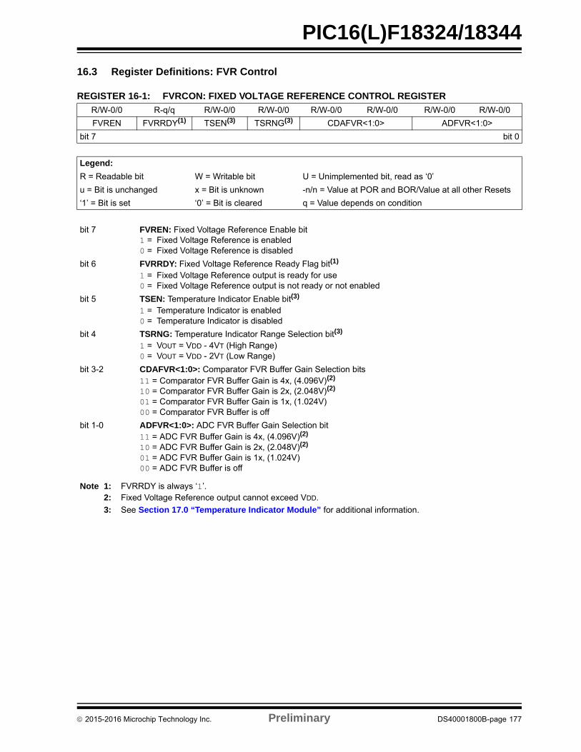
PIC16(L)F18324/18344
16.3 Register Definitions: FVR Control
REGISTER 16-1: FVRCON: FIXED VOLTAGE REFERENCE CONTROL REGISTER
R/W-0/0 R-q/q R/W-0/0 R/W-0/0 R/W-0/0 R/W-0/0 R/W-0/0 R/W-0/0
FVREN FVRRDY(1) TSEN(3) TSRNG(3) CDAFVR<1:0> ADFVR<1:0>
bit 7 bit 0
Legend:
R = Readable bit W = Writable bit U = Unimplemented bit, read as ‘0’
u = Bit is unchanged x = Bit is unknown -n/n = Value at POR and BOR/Value at all other Resets
‘1’ = Bit is set ‘0’ = Bit is cleared q = Value depends on condition
bit 7 FVREN: Fixed Voltage Reference Enable bit1 = Fixed Voltage Reference is enabled0 = Fixed Voltage Reference is disabled
bit 6 FVRRDY: Fixed Voltage Reference Ready Flag bit(1)
1 = Fixed Voltage Reference output is ready for use0 = Fixed Voltage Reference output is not ready or not enabled
bit 5 TSEN: Temperature Indicator Enable bit(3)
1 = Temperature Indicator is enabled0 = Temperature Indicator is disabled
bit 4 TSRNG: Temperature Indicator Range Selection bit(3)
1 = VOUT = VDD - 4VT (High Range)0 = VOUT = VDD - 2VT (Low Range)
bit 3-2 CDAFVR<1:0>: Comparator FVR Buffer Gain Selection bits11 = Comparator FVR Buffer Gain is 4x, (4.096V)(2)
10 = Comparator FVR Buffer Gain is 2x, (2.048V)(2)
01 = Comparator FVR Buffer Gain is 1x, (1.024V)00 = Comparator FVR Buffer is off
bit 1-0 ADFVR<1:0>: ADC FVR Buffer Gain Selection bit11 = ADC FVR Buffer Gain is 4x, (4.096V)(2)
10 = ADC FVR Buffer Gain is 2x, (2.048V)(2)
01 = ADC FVR Buffer Gain is 1x, (1.024V)00 = ADC FVR Buffer is off
Note 1: FVRRDY is always ‘1’.2: Fixed Voltage Reference output cannot exceed VDD.
3: See Section 17.0 “Temperature Indicator Module” for additional information.
2015-2016 Microchip Technology Inc. Preliminary DS40001800B-page 177
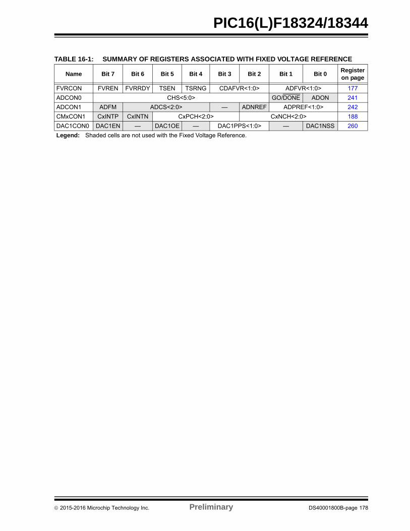
PIC16(L)F18324/18344
TABLE 16-1: SUMMARY OF REGISTERS ASSOCIATED WITH FIXED VOLTAGE REFERENCE
Name Bit 7 Bit 6 Bit 5 Bit 4 Bit 3 Bit 2 Bit 1 Bit 0Register on page
FVRCON FVREN FVRRDY TSEN TSRNG CDAFVR<1:0> ADFVR<1:0> 177
ADCON0 CHS<5:0> GO/DONE ADON 241
ADCON1 ADFM ADCS<2:0> — ADNREF ADPREF<1:0> 242
CMxCON1 CxINTP CxINTN CxPCH<2:0> CxNCH<2:0> 188
DAC1CON0 DAC1EN — DAC1OE — DAC1PPS<1:0> — DAC1NSS 260
Legend: Shaded cells are not used with the Fixed Voltage Reference.
2015-2016 Microchip Technology Inc. Preliminary DS40001800B-page 178
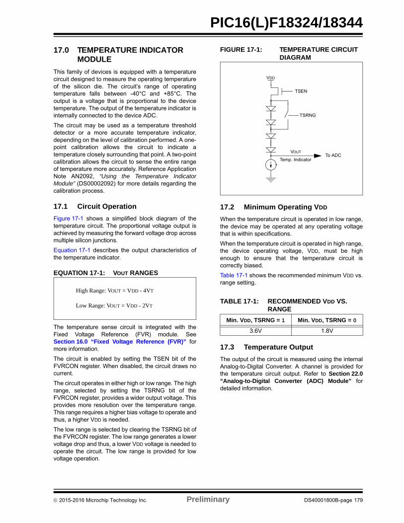
PIC16(L)F18324/18344
17.0 TEMPERATURE INDICATOR MODULE
This family of devices is equipped with a temperaturecircuit designed to measure the operating temperatureof the silicon die. The circuit’s range of operatingtemperature falls between -40°C and +85°C. Theoutput is a voltage that is proportional to the devicetemperature. The output of the temperature indicator isinternally connected to the device ADC.
The circuit may be used as a temperature thresholddetector or a more accurate temperature indicator,depending on the level of calibration performed. A one-point calibration allows the circuit to indicate atemperature closely surrounding that point. A two-pointcalibration allows the circuit to sense the entire rangeof temperature more accurately. Reference ApplicationNote AN2092, “Using the Temperature IndicatorModule” (DS00002092) for more details regarding thecalibration process.
17.1 Circuit Operation
Figure 17-1 shows a simplified block diagram of thetemperature circuit. The proportional voltage output isachieved by measuring the forward voltage drop acrossmultiple silicon junctions.
Equation 17-1 describes the output characteristics ofthe temperature indicator.
EQUATION 17-1: VOUT RANGES
The temperature sense circuit is integrated with theFixed Voltage Reference (FVR) module. SeeSection 16.0 “Fixed Voltage Reference (FVR)” formore information.
The circuit is enabled by setting the TSEN bit of theFVRCON register. When disabled, the circuit draws nocurrent.
The circuit operates in either high or low range. The highrange, selected by setting the TSRNG bit of theFVRCON register, provides a wider output voltage. Thisprovides more resolution over the temperature range.This range requires a higher bias voltage to operate andthus, a higher VDD is needed.
The low range is selected by clearing the TSRNG bit ofthe FVRCON register. The low range generates a lowervoltage drop and thus, a lower VDD voltage is needed tooperate the circuit. The low range is provided for lowvoltage operation.
FIGURE 17-1: TEMPERATURE CIRCUIT DIAGRAM
17.2 Minimum Operating VDD
When the temperature circuit is operated in low range,the device may be operated at any operating voltagethat is within specifications.
When the temperature circuit is operated in high range,the device operating voltage, VDD, must be highenough to ensure that the temperature circuit iscorrectly biased.
Table 17-1 shows the recommended minimum VDD vs.range setting.
17.3 Temperature Output
The output of the circuit is measured using the internalAnalog-to-Digital Converter. A channel is provided forthe temperature circuit output. Refer to Section 22.0“Analog-to-Digital Converter (ADC) Module” fordetailed information.
High Range: VOUT = VDD - 4VT
Low Range: VOUT = VDD - 2VTTABLE 17-1: RECOMMENDED VDD VS.
RANGE
Min. VDD, TSRNG = 1 Min. VDD, TSRNG = 0
3.6V 1.8V
TSEN
TSRNG
VDD
VOUTTo ADC
Temp. Indicator
2015-2016 Microchip Technology Inc. Preliminary DS40001800B-page 179
PIC16(L)F18324/18344
17.4 ADC Acquisition Time
To ensure accurate temperature measurements, theuser must wait at least 200 s after the ADC inputmultiplexer is connected to the temperature indicatoroutput before the conversion is performed.
TABLE 17-2: SUMMARY OF REGISTERS ASSOCIATED WITH THE TEMPERATURE INDICATOR
Name Bit 7 Bit 6 Bit 5 Bit 4 Bit 3 Bit 2 Bit 1 Bit 0Register on page
FVRCON FVREN FVRRDY TSEN TSRNG CDAFVR<1:0> ADFVR<1:0> 177
Legend: Shaded cells are unused by the temperature indicator module.
2015-2016 Microchip Technology Inc. Preliminary DS40001800B-page 180
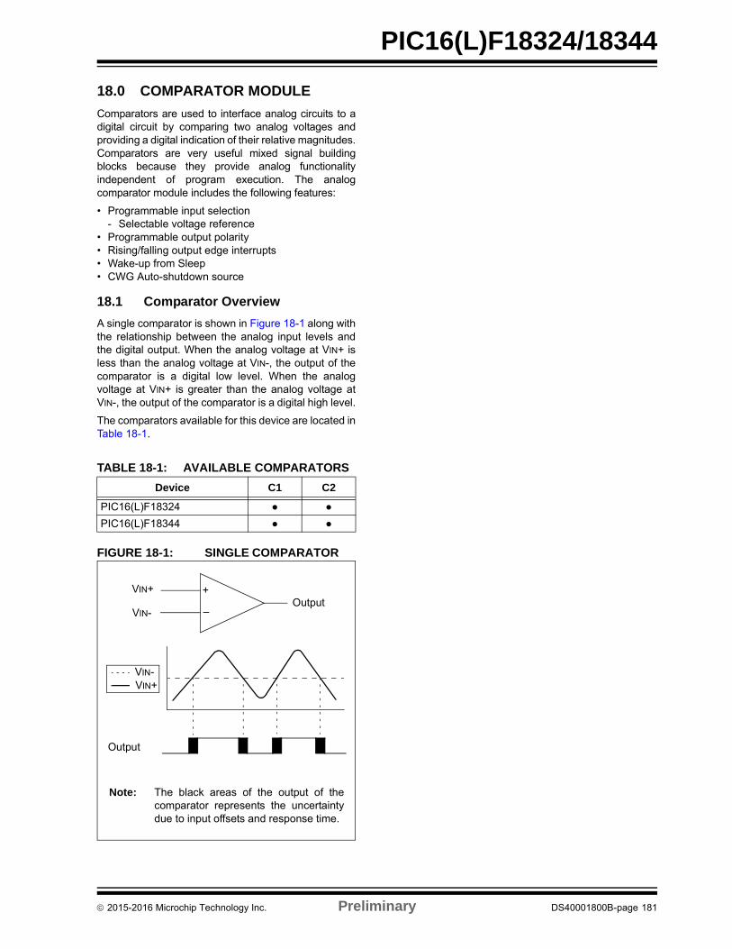
PIC16(L)F18324/18344
18.0 COMPARATOR MODULE
Comparators are used to interface analog circuits to adigital circuit by comparing two analog voltages andproviding a digital indication of their relative magnitudes.Comparators are very useful mixed signal buildingblocks because they provide analog functionalityindependent of program execution. The analogcomparator module includes the following features:
• Programmable input selection- Selectable voltage reference
• Programmable output polarity• Rising/falling output edge interrupts• Wake-up from Sleep• CWG Auto-shutdown source
18.1 Comparator Overview
A single comparator is shown in Figure 18-1 along withthe relationship between the analog input levels andthe digital output. When the analog voltage at VIN+ isless than the analog voltage at VIN-, the output of thecomparator is a digital low level. When the analogvoltage at VIN+ is greater than the analog voltage atVIN-, the output of the comparator is a digital high level.
The comparators available for this device are located inTable 18-1.
FIGURE 18-1: SINGLE COMPARATOR
TABLE 18-1: AVAILABLE COMPARATORS
Device C1 C2
PIC16(L)F18324
PIC16(L)F18344
–
+VIN+
VIN-Output
Output
VIN+VIN-
Note: The black areas of the output of thecomparator represents the uncertaintydue to input offsets and response time.
2015-2016 Microchip Technology Inc. Preliminary DS40001800B-page 181
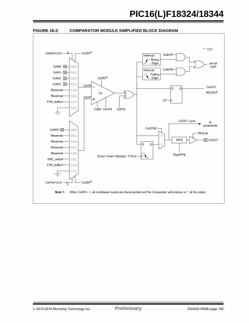
PIC16(L)F18324/18344
FIGURE 18-2: COMPARATOR MODULE SIMPLIFIED BLOCK DIAGRAM
Rev. 10-000027M9/20/2016
CxIN0-
CxIN1-
CxIN0+
FVR_buffer2
DAC_output
+
CxVN
CxVP
CxPCH<2:0>
CxNCH<2:0>
2
3
CxON(1)
CxON(1)
CxON(1)
CxSP CxHYS
InterruptRising Edge
D Q
Q1
CxINTP
CxINTN
CxOUT
MCxOUT
D Q
0
1
CxSYNC
set bitCxIF
TRIS bit
CxOUT
CxOUT_sync
-
InterruptFalling Edge
FVR_buffer2
CxPOL
Cx
(From Timer1 Module) T1CLK
to peripherals
Note 1: When CxON = 0, all multiplexer inputs are disconnected and the Comparator will produce a ‘0’ at the output.
000
011010001
100101110111
Reserved
CxIN2-
CxIN3-
PPS
RxyPPS
000
011010001
100101110111
Reserved
Reserved
Reserved
Reserved
Reserved
2015-2016 Microchip Technology Inc. Preliminary DS40001800B-page 182
PIC16(L)F18324/18344
18.2 Comparator Control
Each comparator has two control registers: CMxCON0and CMxCON1.
The CMxCON0 register (see Register 18-1) containsControl and Status bits for the following:
• Enable• Output• Output polarity• Hysteresis enable• Timer1 output synchronization
The CMxCON1 register (see Register 18-2) containsControl bits for the following:
• Interrupt on positive/negative edge enables• Positive input channel selection• Negative input channel selection
18.2.1 COMPARATOR ENABLE
Setting the CxON bit of the CMxCON0 register enablesthe comparator for operation. Clearing the CxON bitdisables the comparator resulting in minimum currentconsumption.
18.2.2 COMPARATOR OUTPUT
The output of the comparator can be monitored byreading either the CxOUT bit of the CMxCON0 registeror the MCxOUT bit of the CMOUT register.
The comparator output can also be routed to anexternal pin through the RxyPPS register(Register 13-2). The corresponding TRIS bit must beclear to enable the pin as an output.
18.2.3 COMPARATOR OUTPUT POLARITY
Inverting the output of the comparator is functionallyequivalent to swapping the comparator inputs. Thepolarity of the comparator output can be inverted bysetting the CxPOL bit of the CMxCON0 register.Clearing the CxPOL bit results in a non-inverted output.
Table 18-2 shows the output state versus inputconditions, including polarity control.
18.3 Comparator Hysteresis
A selectable amount of separation voltage can beadded to the input pins of each comparator to provide ahysteresis function to the overall operation. Hysteresisis enabled by setting the CxHYS bit of the CMxCON0register.
See Comparator Specifications in Table 35-14 for moreinformation.
18.4 Timer1 Gate Operation
The output resulting from a comparator operation canbe used as a source for gate control of Timer1. SeeSection 27.5 “Timer1 Gate” for more information.This feature is useful for timing the duration or intervalof an analog event.
It is recommended that the comparator output besynchronized to Timer1. This ensures that Timer1 doesnot increment while a change in the comparator isoccurring.
18.4.1 COMPARATOR OUTPUT SYNCHRONIZATION
The output from a comparator can be synchronizedwith Timer1 by setting the CxSYNC bit of theCMxCON0 register.
Once enabled, the comparator output is latched on thefalling edge of the Timer1 source clock. This allows thetimer/counter to synchronize with the CxOUT bit sothat the software sees no ambiguity due to timing. Seethe Comparator Block Diagram (Figure 18-2) and theTimer1 Block Diagram (Figure 27-1) for moreinformation.
Note 1: The internal output of the comparator islatched with each instruction cycle.Unless otherwise specified, externaloutputs are not latched.
TABLE 18-2: COMPARATOR OUTPUT STATE VS. INPUT CONDITIONS
Input Condition CxPOL CxOUT
CxVN > CxVP 0 0
CxVN < CxVP 0 1
CxVN > CxVP 1 1
CxVN < CxVP 1 0
2015-2016 Microchip Technology Inc. Preliminary DS40001800B-page 183
PIC16(L)F18324/18344
18.5 Comparator Interrupt
An interrupt can be generated when either the risingedge or falling edge detector detects a change in theoutput value of each comparator.
When either edge detector is triggered and itsassociated enable bit is set (CxINTP and/or CxINTNbits of the CMxCON1 register), the CorrespondingInterrupt Flag bit (CxIF bit of the PIR2 register) will beset.
To enable the interrupt, you must set the following bits:
• CxON bit of the CMxCON0 register• CxIE bit of the PIE2 register• CxINTP bit of the CMxCON1 register (for a rising
edge detection)• CxINTN bit of the CMxCON1 register (for a falling
edge detection)• PEIE and GIE bits of the INTCON register
The associated interrupt flag bit, CxIF bit of the PIR2register, must be cleared in software. If another edge isdetected while this flag is being cleared, the flag will stillbe set at the end of the sequence.
18.6 Comparator Positive Input Selection
Configuring the CxPCH<2:0> bits of the CMxCON1register directs an internal voltage reference or ananalog pin to the non-inverting input of the comparator:
• CxIN0+ analog pin• DAC output• FVR (Fixed Voltage Reference)• VSS (Ground)
See Section 16.0 “Fixed Voltage Reference (FVR)”for more information on the Fixed Voltage Referencemodule.
See Section 24.0 “5-Bit Digital-to-Analog Converter(DAC1) Module” for more information on the DACinput signal.
Any time the comparator is disabled (CxON = 0), allcomparator inputs are disabled.
18.7 Comparator Negative Input Selection
The CxNCH<2:0> bits of the CMxCON1 register directan analog input pin and internal reference voltage oranalog ground to the inverting input of the comparator:
• CxIN- pin• FVR (Fixed Voltage Reference)• Analog Ground
18.8 Comparator Response Time
The comparator output is indeterminate for a period oftime after the change of an input source or the selectionof a new reference voltage. This period is referred to asthe response time. The response time of the comparatordiffers from the settling time of the voltage reference.Therefore, both of these times must be considered whendetermining the total response time to a comparatorinput change. See the Comparator and VoltageReference Specifications in Table 35-14 for moredetails.
Note: Although a comparator is disabled, aninterrupt can be generated by changingthe output polarity with the CxPOL bit ofthe CMxCON0 register, or by switchingthe comparator on or off with the CxON bitof the CMxCON0 register.
Note: To use CxINy+ and CxINy- pins as analoginput, the appropriate bits must be set inthe ANSEL register and the correspond-ing TRIS bits must also be set to disablethe output drivers.
2015-2016 Microchip Technology Inc. Preliminary DS40001800B-page 184
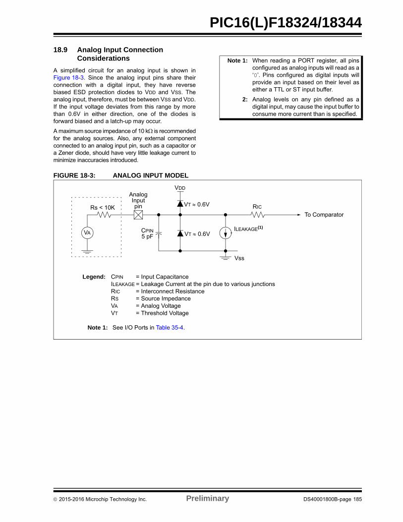
PIC16(L)F18324/18344
18.9 Analog Input Connection Considerations
A simplified circuit for an analog input is shown inFigure 18-3. Since the analog input pins share theirconnection with a digital input, they have reversebiased ESD protection diodes to VDD and VSS. Theanalog input, therefore, must be between VSS and VDD.If the input voltage deviates from this range by morethan 0.6V in either direction, one of the diodes isforward biased and a latch-up may occur.
A maximum source impedance of 10 k is recommendedfor the analog sources. Also, any external componentconnected to an analog input pin, such as a capacitor ora Zener diode, should have very little leakage current tominimize inaccuracies introduced.
FIGURE 18-3: ANALOG INPUT MODEL
Note 1: When reading a PORT register, all pinsconfigured as analog inputs will read as a‘0’. Pins configured as digital inputs willprovide an input based on their level aseither a TTL or ST input buffer.
2: Analog levels on any pin defined as adigital input, may cause the input buffer toconsume more current than is specified.
VA
Rs < 10K
CPIN5 pF
VDD
VT 0.6V
VT 0.6V
RIC
ILEAKAGE(1)
Vss
Legend: CPIN = Input CapacitanceILEAKAGE = Leakage Current at the pin due to various junctionsRIC = Interconnect ResistanceRS = Source ImpedanceVA = Analog VoltageVT = Threshold Voltage
To Comparator
Note 1: See I/O Ports in Table 35-4.
AnalogInputpin
2015-2016 Microchip Technology Inc. Preliminary DS40001800B-page 185
PIC16(L)F18324/18344
18.10 CWG Auto-shutdown Source
The output of the comparator module can be used asan auto-shutdown source for the CWG module. Whenthe output of the comparator is active and thecorresponding ASxE is enabled, the CWG operationwill be suspended immediately (Section 20.7.1.2“External Input Source Shutdown”).
18.11 Operation in Sleep Mode
The comparator module can operate during Sleep. Thecomparator clock source is based on the Timer1 clocksource. If the Timer1 clock source is either the systemclock (FOSC) or the instruction clock (FOSC/4), Timer1will not operate during Sleep, and synchronizedcomparator outputs will not operate.
A comparator interrupt will wake the device from Sleep.The CxIE bits of the PIE2 register must be set to enablecomparator interrupts.
2015-2016 Microchip Technology Inc. Preliminary DS40001800B-page 186
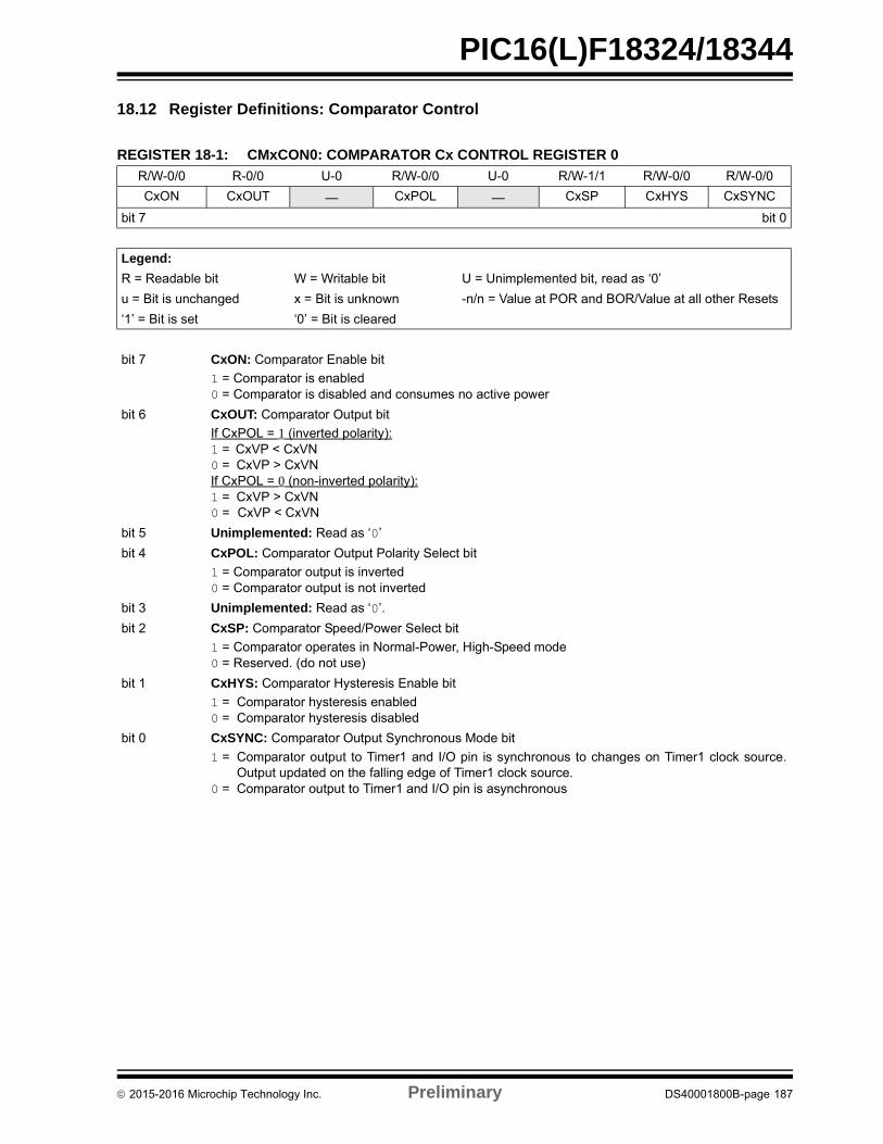
PIC16(L)F18324/18344
18.12 Register Definitions: Comparator Control
REGISTER 18-1: CMxCON0: COMPARATOR Cx CONTROL REGISTER 0
R/W-0/0 R-0/0 U-0 R/W-0/0 U-0 R/W-1/1 R/W-0/0 R/W-0/0
CxON CxOUT — CxPOL — CxSP CxHYS CxSYNC
bit 7 bit 0
Legend:
R = Readable bit W = Writable bit U = Unimplemented bit, read as ‘0’
u = Bit is unchanged x = Bit is unknown -n/n = Value at POR and BOR/Value at all other Resets
‘1’ = Bit is set ‘0’ = Bit is cleared
bit 7 CxON: Comparator Enable bit
1 = Comparator is enabled0 = Comparator is disabled and consumes no active power
bit 6 CxOUT: Comparator Output bit
If CxPOL = 1 (inverted polarity):1 = CxVP < CxVN0 = CxVP > CxVNIf CxPOL = 0 (non-inverted polarity):1 = CxVP > CxVN0 = CxVP < CxVN
bit 5 Unimplemented: Read as ‘0’
bit 4 CxPOL: Comparator Output Polarity Select bit
1 = Comparator output is inverted0 = Comparator output is not inverted
bit 3 Unimplemented: Read as ‘0’.
bit 2 CxSP: Comparator Speed/Power Select bit
1 = Comparator operates in Normal-Power, High-Speed mode0 = Reserved. (do not use)
bit 1 CxHYS: Comparator Hysteresis Enable bit
1 = Comparator hysteresis enabled0 = Comparator hysteresis disabled
bit 0 CxSYNC: Comparator Output Synchronous Mode bit
1 = Comparator output to Timer1 and I/O pin is synchronous to changes on Timer1 clock source.Output updated on the falling edge of Timer1 clock source.
0 = Comparator output to Timer1 and I/O pin is asynchronous
2015-2016 Microchip Technology Inc. Preliminary DS40001800B-page 187
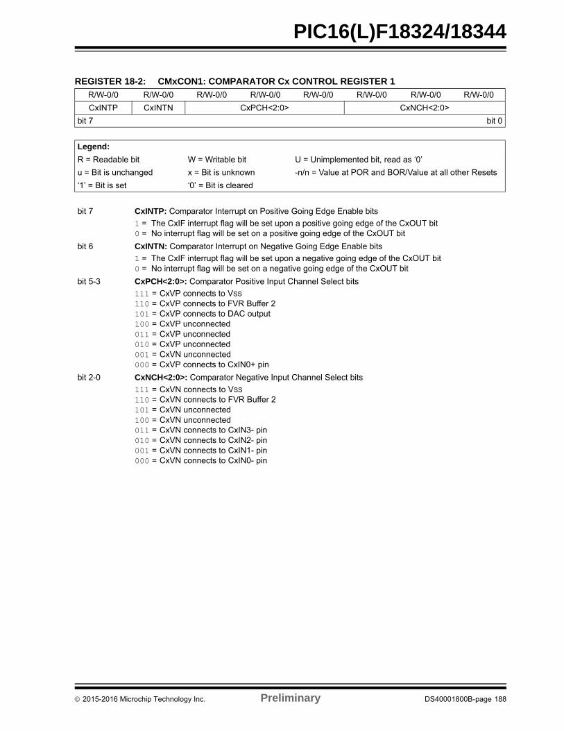
PIC16(L)F18324/18344
REGISTER 18-2: CMxCON1: COMPARATOR Cx CONTROL REGISTER 1
R/W-0/0 R/W-0/0 R/W-0/0 R/W-0/0 R/W-0/0 R/W-0/0 R/W-0/0 R/W-0/0
CxINTP CxINTN CxPCH<2:0> CxNCH<2:0>
bit 7 bit 0
Legend:
R = Readable bit W = Writable bit U = Unimplemented bit, read as ‘0’
u = Bit is unchanged x = Bit is unknown -n/n = Value at POR and BOR/Value at all other Resets
‘1’ = Bit is set ‘0’ = Bit is cleared
bit 7 CxINTP: Comparator Interrupt on Positive Going Edge Enable bits
1 = The CxIF interrupt flag will be set upon a positive going edge of the CxOUT bit0 = No interrupt flag will be set on a positive going edge of the CxOUT bit
bit 6 CxINTN: Comparator Interrupt on Negative Going Edge Enable bits
1 = The CxIF interrupt flag will be set upon a negative going edge of the CxOUT bit0 = No interrupt flag will be set on a negative going edge of the CxOUT bit
bit 5-3 CxPCH<2:0>: Comparator Positive Input Channel Select bits
111 = CxVP connects to VSS
110 = CxVP connects to FVR Buffer 2101 = CxVP connects to DAC output100 = CxVP unconnected011 = CxVP unconnected010 = CxVP unconnected001 = CxVN unconnected000 = CxVP connects to CxIN0+ pin
bit 2-0 CxNCH<2:0>: Comparator Negative Input Channel Select bits
111 = CxVN connects to VSS
110 = CxVN connects to FVR Buffer 2101 = CxVN unconnected100 = CxVN unconnected011 = CxVN connects to CxIN3- pin010 = CxVN connects to CxIN2- pin001 = CxVN connects to CxIN1- pin000 = CxVN connects to CxIN0- pin
2015-2016 Microchip Technology Inc. Preliminary DS40001800B-page 188
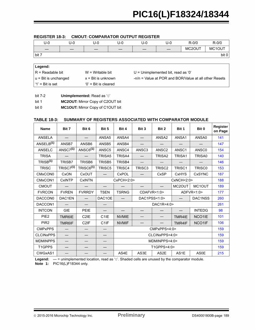
PIC16(L)F18324/18344
REGISTER 18-3: CMOUT: COMPARATOR OUTPUT REGISTER
U-0 U-0 U-0 U-0 U-0 U-0 R-0/0 R-0/0
— — — — — — MC2OUT MC1OUT
bit 7 bit 0
Legend:
R = Readable bit W = Writable bit U = Unimplemented bit, read as ‘0’
u = Bit is unchanged x = Bit is unknown -n/n = Value at POR and BOR/Value at all other Resets
‘1’ = Bit is set ‘0’ = Bit is cleared
bit 7-2 Unimplemented: Read as ‘0’
bit 1 MC2OUT: Mirror Copy of C2OUT bit
bit 0 MC1OUT: Mirror Copy of C1OUT bit
TABLE 18-3: SUMMARY OF REGISTERS ASSOCIATED WITH COMPARATOR MODULE
Name Bit 7 Bit 6 Bit 5 Bit 4 Bit 3 Bit 2 Bit 1 Bit 0Register on Page
ANSELA ― ― ANSA5 ANSA4 ― ANSA2 ANSA1 ANSA0 141
ANSELB(1) ANSB7 ANSB6 ANSB5 ANSB4 ― ― ― ― 147
ANSELC ANSC7(1) ANSC6(1) ANSC5 ANSC4 ANSC3 ANSC2 ANSC1 ANSC0 154
TRISA ― ― TRISA5 TRISA4 ― TRISA2 TRISA1 TRISA0 140
TRISB(1) TRISB7 TRISB6 TRISB5 TRISB4 ― ― ― ― 146
TRISC TRISC7(1) TRISC6(1) TRISC5 TRISC4 TRISC3 TRISC2 TRISC1 TRISC0 153
CMxCON0 CxON CxOUT ― CxPOL ― CxSP CxHYS CxSYNC 187
CMxCON1 CxINTP CxINTN CxPCH<2:0> CxNCH<2:0> 188
CMOUT ― ― ― ― ― ― MC2OUT MC1OUT 189
FVRCON FVREN FVRRDY TSEN TSRNG CDAFVR<1:0> ADFVR<1:0> 177
DACCON0 DAC1EN ― DAC1OE ― DAC1PSS<1:0> ― DAC1NSS 260
DACCON1 ― ― ― DAC1R<4:0> 261
INTCON GIE PEIE ― ― ― ― ― INTEDG 98
PIE2 TMR6IE C2IE C1IE NVMIE ― ― TMR4IE NCO1IE 101
PIR2 TMR6IF C2IF C1IF NVMIF ― ― TMR4IF NCO1IF 106
CMPxPPS ― ― ― CMPxPPS<4:0> 159
CLCINxPPS ― ― ― CLCINxPPS<4:0> 159
MDMINPPS ― ― ― MDMINPPS<4:0> 159
T1GPPS ― ― ― T1GPPS<4:0> 159
CWGxAS1 ― ― ― AS4E AS3E AS2E AS1E AS0E 215
Legend: — = unimplemented location, read as ‘0’. Shaded cells are unused by the comparator module.Note 1: PIC16(L)F18344 only.
2015-2016 Microchip Technology Inc. Preliminary DS40001800B-page 189
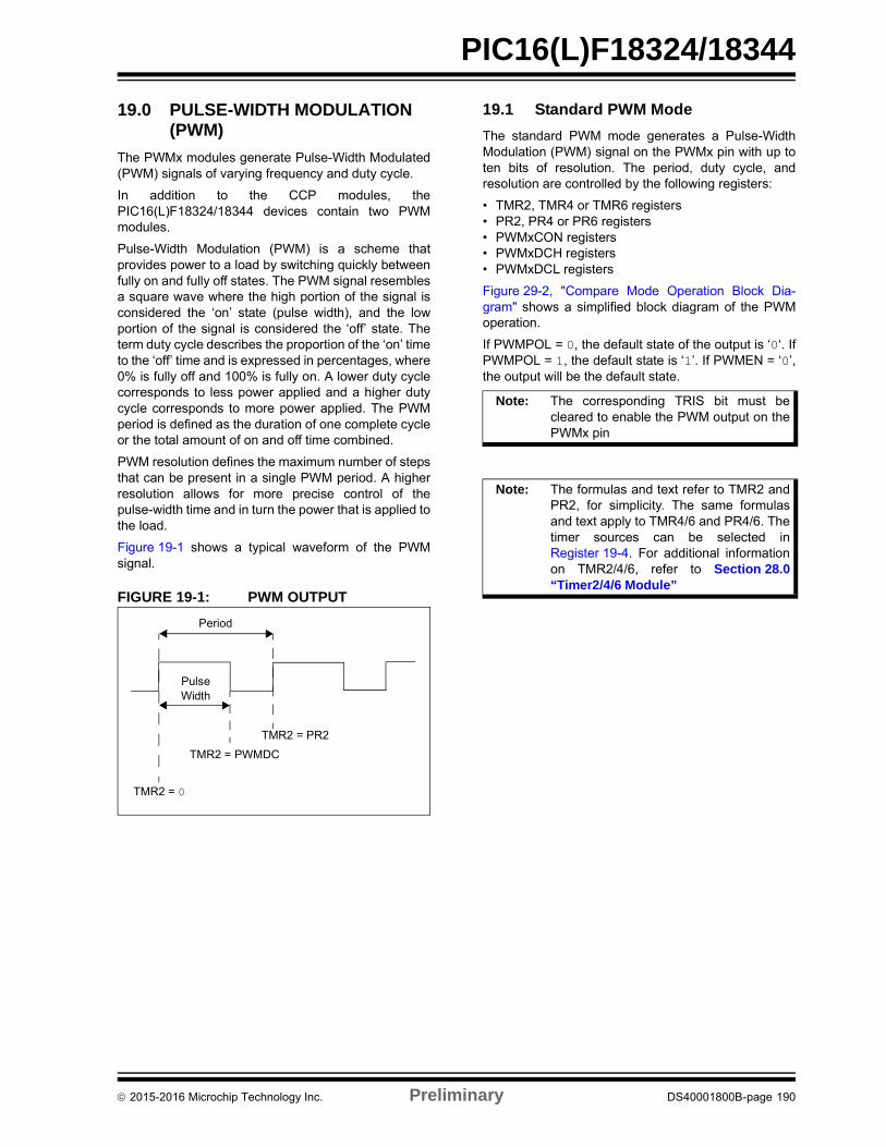
PIC16(L)F18324/18344
19.0 PULSE-WIDTH MODULATION (PWM)
The PWMx modules generate Pulse-Width Modulated(PWM) signals of varying frequency and duty cycle.
In addition to the CCP modules, thePIC16(L)F18324/18344 devices contain two PWMmodules.
Pulse-Width Modulation (PWM) is a scheme thatprovides power to a load by switching quickly betweenfully on and fully off states. The PWM signal resemblesa square wave where the high portion of the signal isconsidered the ‘on’ state (pulse width), and the lowportion of the signal is considered the ‘off’ state. Theterm duty cycle describes the proportion of the ‘on’ timeto the ‘off’ time and is expressed in percentages, where0% is fully off and 100% is fully on. A lower duty cyclecorresponds to less power applied and a higher dutycycle corresponds to more power applied. The PWMperiod is defined as the duration of one complete cycleor the total amount of on and off time combined.
PWM resolution defines the maximum number of stepsthat can be present in a single PWM period. A higherresolution allows for more precise control of thepulse-width time and in turn the power that is applied tothe load.
Figure 19-1 shows a typical waveform of the PWMsignal.
FIGURE 19-1: PWM OUTPUT
19.1 Standard PWM Mode
The standard PWM mode generates a Pulse-WidthModulation (PWM) signal on the PWMx pin with up toten bits of resolution. The period, duty cycle, andresolution are controlled by the following registers:
• TMR2, TMR4 or TMR6 registers• PR2, PR4 or PR6 registers• PWMxCON registers• PWMxDCH registers• PWMxDCL registers
Figure 29-2, "Compare Mode Operation Block Dia-gram" shows a simplified block diagram of the PWMoperation.
If PWMPOL = 0, the default state of the output is ‘0‘. IfPWMPOL = 1, the default state is ‘1’. If PWMEN = ‘0’,the output will be the default state.
Period
Pulse Width
TMR2 = 0
TMR2 = PWMDC
TMR2 = PR2
Note: The corresponding TRIS bit must becleared to enable the PWM output on thePWMx pin
Note: The formulas and text refer to TMR2 andPR2, for simplicity. The same formulasand text apply to TMR4/6 and PR4/6. Thetimer sources can be selected inRegister 19-4. For additional informationon TMR2/4/6, refer to Section 28.0“Timer2/4/6 Module”
2015-2016 Microchip Technology Inc. Preliminary DS40001800B-page 190
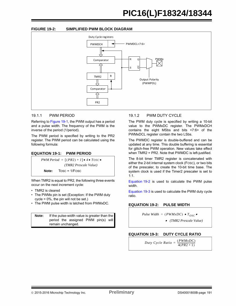
PIC16(L)F18324/18344
FIGURE 19-2: SIMPLIFIED PWM BLOCK DIAGRAM
19.1.1 PWM PERIOD
Referring to Figure 19-1, the PWM output has a periodand a pulse width. The frequency of the PWM is theinverse of the period (1/period).
The PWM period is specified by writing to the PR2register. The PWM period can be calculated using thefollowing formula:
EQUATION 19-1: PWM PERIOD
When TMR2 is equal to PR2, the following three eventsoccur on the next increment cycle:
• TMR2 is cleared• The PWMx pin is set (Exception: If the PWM duty
cycle = 0%, the pin will not be set.)• The PWM pulse width is latched from PWMxDC.
19.1.2 PWM DUTY CYCLE
The PWM duty cycle is specified by writing a 10-bitvalue to the PWMxDC register. The PWMxDCHcontains the eight MSbs and bits <7:6> of thePWMxDCL register contain the two LSbs.
The PWMDC register is double-buffered and can beupdated at any time. This double buffering is essentialfor glitch-free PWM operation. New values take effectwhen TMR2 = PR2. Note that PWMDC is left-justified.
The 8-bit timer TMR2 register is concatenated witheither the 2-bit internal system clock (FOSC), or two bitsof the prescaler, to create the 10-bit time base. Thesystem clock is used if the Timer2 prescaler is set to1:1.
Equation 19-2 is used to calculate the PWM pulsewidth.
Equation 19-3 is used to calculate the PWM duty cycleratio.
EQUATION 19-2: PULSE WIDTH
EQUATION 19-3: DUTY CYCLE RATIO
R
S
Q
Q
Duty Cycle registers
PWMDCH PWMDCL<7:6>
Comparator
Comparator
TMR2
PR2
Output Polarity (PWMPOL)
PWMx
R
Note: If the pulse-width value is greater than theperiod the assigned PWM pin(s) willremain unchanged.
PWM Period PR2 1+ 4 TOSC =
(TMR2 Prescale Value)
Note: TOSC = 1/FOSC
Pulse Width PWMxDC TOSC =
(TMR2 Prescale Value)
Duty Cycle RatioPWMxDC 4 PR2 1+ -------------------------------=
2015-2016 Microchip Technology Inc. Preliminary DS40001800B-page 191
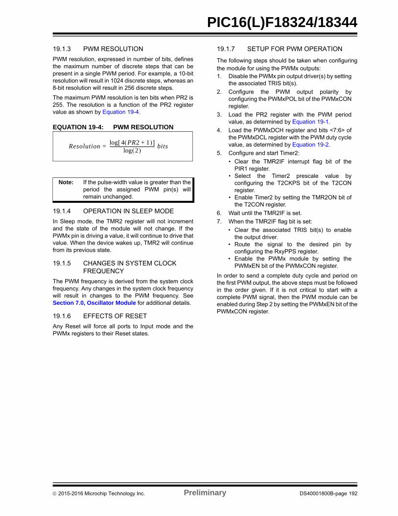
PIC16(L)F18324/18344
19.1.3 PWM RESOLUTION
PWM resolution, expressed in number of bits, definesthe maximum number of discrete steps that can bepresent in a single PWM period. For example, a 10-bitresolution will result in 1024 discrete steps, whereas an8-bit resolution will result in 256 discrete steps.
The maximum PWM resolution is ten bits when PR2 is255. The resolution is a function of the PR2 registervalue as shown by Equation 19-4.
EQUATION 19-4: PWM RESOLUTION
19.1.4 OPERATION IN SLEEP MODE
In Sleep mode, the TMR2 register will not incrementand the state of the module will not change. If thePWMx pin is driving a value, it will continue to drive thatvalue. When the device wakes up, TMR2 will continuefrom its previous state.
19.1.5 CHANGES IN SYSTEM CLOCK FREQUENCY
The PWM frequency is derived from the system clockfrequency. Any changes in the system clock frequencywill result in changes to the PWM frequency. SeeSection 7.0, Oscillator Module for additional details.
19.1.6 EFFECTS OF RESET
Any Reset will force all ports to Input mode and thePWMx registers to their Reset states.
19.1.7 SETUP FOR PWM OPERATION
The following steps should be taken when configuringthe module for using the PWMx outputs:1. Disable the PWMx pin output driver(s) by setting
the associated TRIS bit(s).
2. Configure the PWM output polarity byconfiguring the PWMxPOL bit of the PWMxCONregister.
3. Load the PR2 register with the PWM periodvalue, as determined by Equation 19-1.
4. Load the PWMxDCH register and bits <7:6> ofthe PWMxDCL register with the PWM duty cyclevalue, as determined by Equation 19-2.
5. Configure and start Timer2:
• Clear the TMR2IF interrupt flag bit of thePIR1 register.
• Select the Timer2 prescale value byconfiguring the T2CKPS bit of the T2CONregister.
• Enable Timer2 by setting the TMR2ON bit ofthe T2CON register.
6. Wait until the TMR2IF is set.
7. When the TMR2IF flag bit is set:
• Clear the associated TRIS bit(s) to enablethe output driver.
• Route the signal to the desired pin byconfiguring the RxyPPS register.
• Enable the PWMx module by setting thePWMxEN bit of the PWMxCON register.
In order to send a complete duty cycle and period onthe first PWM output, the above steps must be followedin the order given. If it is not critical to start with acomplete PWM signal, then the PWM module can beenabled during Step 2 by setting the PWMxEN bit of thePWMxCON register.
Note: If the pulse-width value is greater than theperiod the assigned PWM pin(s) willremain unchanged.
Resolution 4 PR2 1+ log
2 log----------------------------------------- bits=
2015-2016 Microchip Technology Inc. Preliminary DS40001800B-page 192
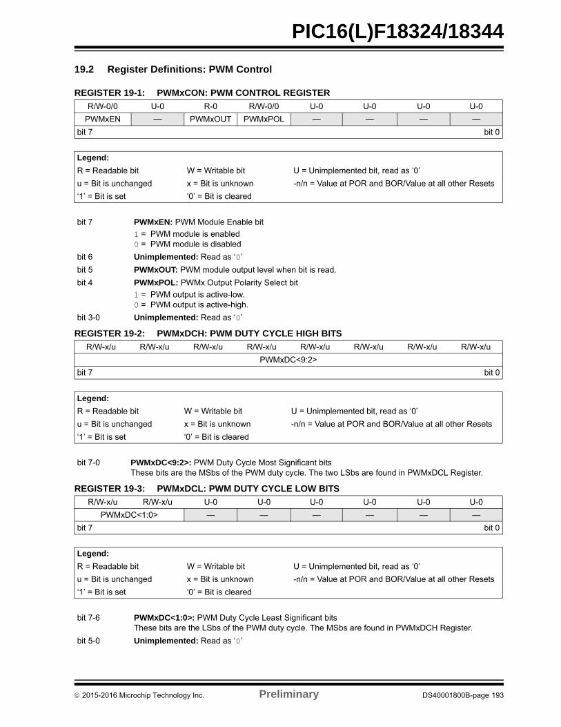
PIC16(L)F18324/18344
19.2 Register Definitions: PWM Control
REGISTER 19-1: PWMxCON: PWM CONTROL REGISTER
R/W-0/0 U-0 R-0 R/W-0/0 U-0 U-0 U-0 U-0
PWMxEN — PWMxOUT PWMxPOL — — — —
bit 7 bit 0
Legend:
R = Readable bit W = Writable bit U = Unimplemented bit, read as ‘0’
u = Bit is unchanged x = Bit is unknown -n/n = Value at POR and BOR/Value at all other Resets
‘1’ = Bit is set ‘0’ = Bit is cleared
bit 7 PWMxEN: PWM Module Enable bit
1 = PWM module is enabled0 = PWM module is disabled
bit 6 Unimplemented: Read as ‘0’
bit 5 PWMxOUT: PWM module output level when bit is read.
bit 4 PWMxPOL: PWMx Output Polarity Select bit
1 = PWM output is active-low.0 = PWM output is active-high.
bit 3-0 Unimplemented: Read as ‘0’
REGISTER 19-2: PWMxDCH: PWM DUTY CYCLE HIGH BITS
R/W-x/u R/W-x/u R/W-x/u R/W-x/u R/W-x/u R/W-x/u R/W-x/u R/W-x/u
PWMxDC<9:2>
bit 7 bit 0
Legend:
R = Readable bit W = Writable bit U = Unimplemented bit, read as ‘0’
u = Bit is unchanged x = Bit is unknown -n/n = Value at POR and BOR/Value at all other Resets
‘1’ = Bit is set ‘0’ = Bit is cleared
bit 7-0 PWMxDC<9:2>: PWM Duty Cycle Most Significant bitsThese bits are the MSbs of the PWM duty cycle. The two LSbs are found in PWMxDCL Register.
REGISTER 19-3: PWMxDCL: PWM DUTY CYCLE LOW BITS
R/W-x/u R/W-x/u U-0 U-0 U-0 U-0 U-0 U-0
PWMxDC<1:0> — — — — — —
bit 7 bit 0
Legend:
R = Readable bit W = Writable bit U = Unimplemented bit, read as ‘0’
u = Bit is unchanged x = Bit is unknown -n/n = Value at POR and BOR/Value at all other Resets
‘1’ = Bit is set ‘0’ = Bit is cleared
bit 7-6 PWMxDC<1:0>: PWM Duty Cycle Least Significant bitsThese bits are the LSbs of the PWM duty cycle. The MSbs are found in PWMxDCH Register.
bit 5-0 Unimplemented: Read as ‘0’
2015-2016 Microchip Technology Inc. Preliminary DS40001800B-page 193
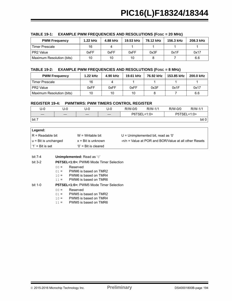
PIC16(L)F18324/18344
TABLE 19-1: EXAMPLE PWM FREQUENCIES AND RESOLUTIONS (FOSC = 20 MHz)
PWM Frequency 1.22 kHz 4.88 kHz 19.53 kHz 78.12 kHz 156.3 kHz 208.3 kHz
Timer Prescale 16 4 1 1 1 1
PR2 Value 0xFF 0xFF 0xFF 0x3F 0x1F 0x17
Maximum Resolution (bits) 10 10 10 8 7 6.6
TABLE 19-2: EXAMPLE PWM FREQUENCIES AND RESOLUTIONS (FOSC = 8 MHz)
PWM Frequency 1.22 kHz 4.90 kHz 19.61 kHz 76.92 kHz 153.85 kHz 200.0 kHz
Timer Prescale 16 4 1 1 1 1
PR2 Value 0xFF 0xFF 0xFF 0x3F 0x1F 0x17
Maximum Resolution (bits) 10 10 10 8 7 6.6
REGISTER 19-4: PWMTMRS: PWM TIMERS CONTROL REGISTER
U-0 U-0 U-0 U-0 R/W-0/0 R/W-1/1 R/W-0/0 R/W-1/1
— — — — P6TSEL<1:0> P5TSEL<1:0>
bit 7 bit 0
Legend:
R = Readable bit W = Writable bit U = Unimplemented bit, read as ‘0’
u = Bit is unchanged x = Bit is unknown -n/n = Value at POR and BOR/Value at all other Resets
‘1’ = Bit is set ‘0’ = Bit is cleared
bit 7-4 Unimplemented: Read as ‘0’
bit 3-2 P6TSEL<1:0>: PWM6 Mode Timer Selection
00 = Reserved01 = PWM6 is based on TMR210 = PWM6 is based on TMR411 = PWM6 is based on TMR6
bit 1-0 P5TSEL<1:0>: PWM5 Mode Timer Selection
00 = Reserved01 = PWM5 is based on TMR210 = PWM5 is based on TMR411 = PWM5 is based on TMR6
2015-2016 Microchip Technology Inc. Preliminary DS40001800B-page 194
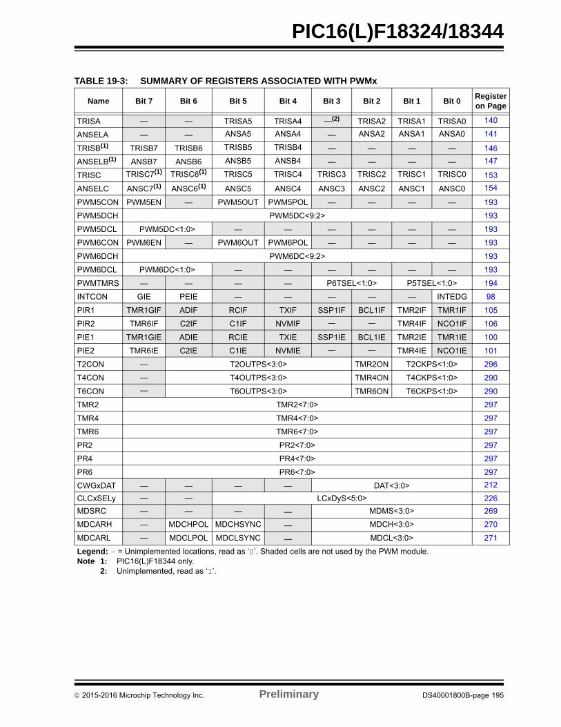
PIC16(L)F18324/18344
TABLE 19-3: SUMMARY OF REGISTERS ASSOCIATED WITH PWMx
Name Bit 7 Bit 6 Bit 5 Bit 4 Bit 3 Bit 2 Bit 1 Bit 0Register on Page
TRISA — — TRISA5 TRISA4 —(2) TRISA2 TRISA1 TRISA0 140
ANSELA — — ANSA5 ANSA4 — ANSA2 ANSA1 ANSA0 141
TRISB(1) TRISB7 TRISB6 TRISB5 TRISB4 — — — — 146
ANSELB(1) ANSB7 ANSB6 ANSB5 ANSB4 — — — — 147
TRISC TRISC7(1) TRISC6(1) TRISC5 TRISC4 TRISC3 TRISC2 TRISC1 TRISC0 153
ANSELC ANSC7(1) ANSC6(1) ANSC5 ANSC4 ANSC3 ANSC2 ANSC1 ANSC0 154
PWM5CON PWM5EN — PWM5OUT PWM5POL — — — — 193
PWM5DCH PWM5DC<9:2> 193
PWM5DCL PWM5DC<1:0> — — — — — — 193
PWM6CON PWM6EN — PWM6OUT PWM6POL — — — — 193
PWM6DCH PWM6DC<9:2> 193
PWM6DCL PWM6DC<1:0> — — — — — — 193
PWMTMRS — — — — P6TSEL<1:0> P5TSEL<1:0> 194
INTCON GIE PEIE — — — — — INTEDG 98
PIR1 TMR1GIF ADIF RCIF TXIF SSP1IF BCL1IF TMR2IF TMR1IF 105
PIR2 TMR6IF C2IF C1IF NVMIF ― ― TMR4IF NCO1IF 106
PIE1 TMR1GIE ADIE RCIE TXIE SSP1IE BCL1IE TMR2IE TMR1IE 100
PIE2 TMR6IE C2IE C1IE NVMIE ― ― TMR4IE NCO1IE 101
T2CON — T2OUTPS<3:0> TMR2ON T2CKPS<1:0> 296
T4CON — T4OUTPS<3:0> TMR4ON T4CKPS<1:0> 290
T6CON — T6OUTPS<3:0> TMR6ON T6CKPS<1:0> 290
TMR2 TMR2<7:0> 297
TMR4 TMR4<7:0> 297
TMR6 TMR6<7:0> 297
PR2 PR2<7:0> 297
PR4 PR4<7:0> 297
PR6 PR6<7:0> 297
CWGxDAT — — — — DAT<3:0> 212
CLCxSELy — — LCxDyS<5:0> 226
MDSRC — — — — MDMS<3:0> 269
MDCARH — MDCHPOL MDCHSYNC — MDCH<3:0> 270
MDCARL — MDCLPOL MDCLSYNC — MDCL<3:0> 271
Legend: - = Unimplemented locations, read as ‘0’. Shaded cells are not used by the PWM module.Note 1: PIC16(L)F18344 only.
2: Unimplemented, read as ‘1’.
2015-2016 Microchip Technology Inc. Preliminary DS40001800B-page 195
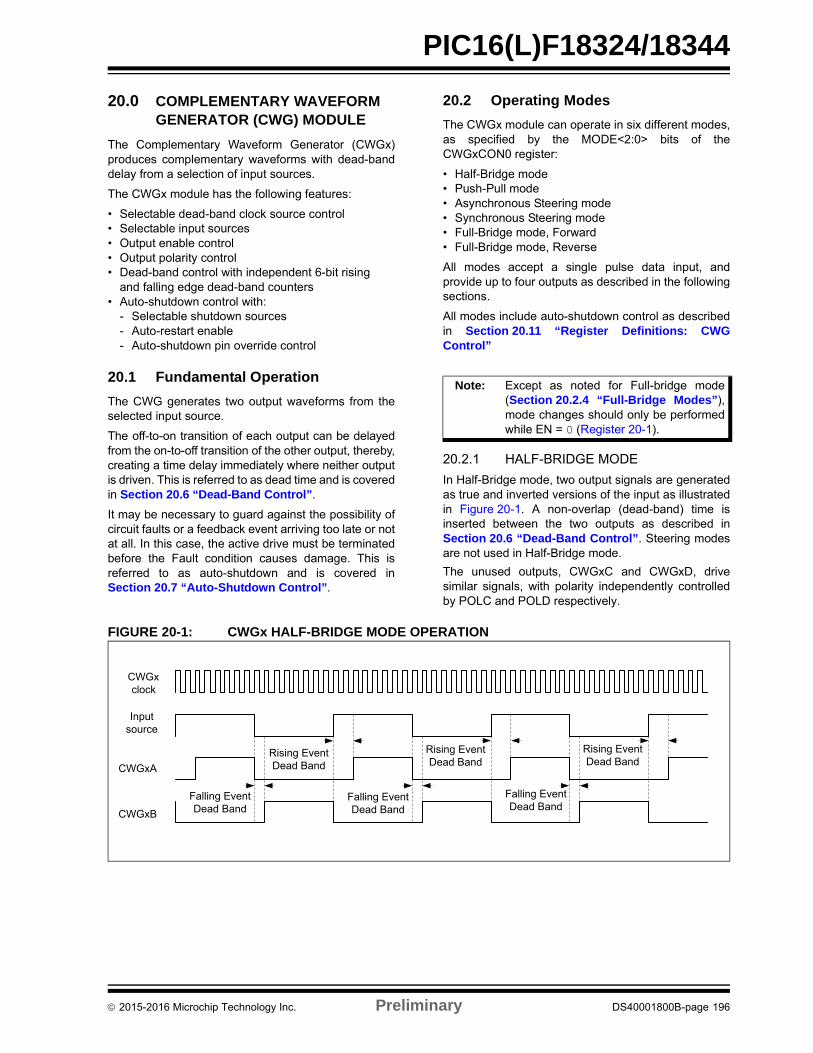
PIC16(L)F18324/18344
20.0 COMPLEMENTARY WAVEFORM GENERATOR (CWG) MODULE
The Complementary Waveform Generator (CWGx)produces complementary waveforms with dead-banddelay from a selection of input sources.
The CWGx module has the following features:
• Selectable dead-band clock source control• Selectable input sources• Output enable control• Output polarity control• Dead-band control with independent 6-bit rising
and falling edge dead-band counters• Auto-shutdown control with:
- Selectable shutdown sources- Auto-restart enable- Auto-shutdown pin override control
20.1 Fundamental Operation
The CWG generates two output waveforms from theselected input source.
The off-to-on transition of each output can be delayedfrom the on-to-off transition of the other output, thereby,creating a time delay immediately where neither outputis driven. This is referred to as dead time and is coveredin Section 20.6 “Dead-Band Control”.
It may be necessary to guard against the possibility ofcircuit faults or a feedback event arriving too late or notat all. In this case, the active drive must be terminatedbefore the Fault condition causes damage. This isreferred to as auto-shutdown and is covered inSection 20.7 “Auto-Shutdown Control”.
20.2 Operating Modes
The CWGx module can operate in six different modes,as specified by the MODE<2:0> bits of theCWGxCON0 register:
• Half-Bridge mode • Push-Pull mode• Asynchronous Steering mode• Synchronous Steering mode• Full-Bridge mode, Forward• Full-Bridge mode, Reverse
All modes accept a single pulse data input, andprovide up to four outputs as described in the followingsections.
All modes include auto-shutdown control as describedin Section 20.11 “Register Definitions: CWGControl”
20.2.1 HALF-BRIDGE MODE
In Half-Bridge mode, two output signals are generatedas true and inverted versions of the input as illustratedin Figure 20-1. A non-overlap (dead-band) time isinserted between the two outputs as described inSection 20.6 “Dead-Band Control”. Steering modesare not used in Half-Bridge mode.
The unused outputs, CWGxC and CWGxD, drivesimilar signals, with polarity independently controlledby POLC and POLD respectively.
FIGURE 20-1: CWGx HALF-BRIDGE MODE OPERATION
Note: Except as noted for Full-bridge mode(Section 20.2.4 “Full-Bridge Modes”),mode changes should only be performedwhile EN = 0 (Register 20-1).
CWGclock
Inputsource
CWG A
CWG B
Falling Event Dead Band
Rising Event Dead Band
Rising Event Dead Band
Falling Event Dead Band
Falling Event Dead Band
Rising Event Dead Band
2015-2016 Microchip Technology Inc. Preliminary DS40001800B-page 196
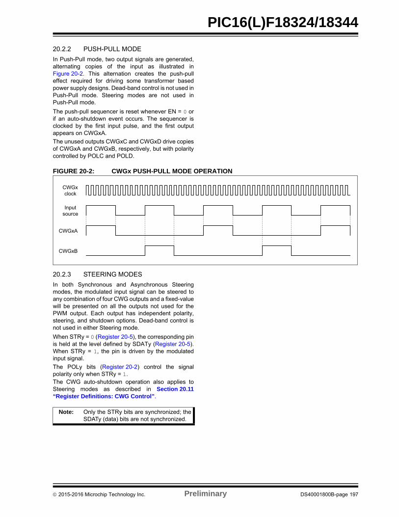
PIC16(L)F18324/18344
20.2.2 PUSH-PULL MODE
In Push-Pull mode, two output signals are generated,alternating copies of the input as illustrated inFigure 20-2. This alternation creates the push-pulleffect required for driving some transformer basedpower supply designs. Dead-band control is not used inPush-Pull mode. Steering modes are not used inPush-Pull mode.
The push-pull sequencer is reset whenever EN = 0 orif an auto-shutdown event occurs. The sequencer isclocked by the first input pulse, and the first outputappears on CWGxA.
The unused outputs CWGxC and CWGxD drive copiesof CWGxA and CWGxB, respectively, but with polaritycontrolled by POLC and POLD.
FIGURE 20-2: CWGx PUSH-PULL MODE OPERATION
20.2.3 STEERING MODES
In both Synchronous and Asynchronous Steeringmodes, the modulated input signal can be steered toany combination of four CWG outputs and a fixed-valuewill be presented on all the outputs not used for thePWM output. Each output has independent polarity,steering, and shutdown options. Dead-band control isnot used in either Steering mode.
When STRy = 0 (Register 20-5), the corresponding pinis held at the level defined by SDATy (Register 20-5).When STRy = 1, the pin is driven by the modulatedinput signal.
The POLy bits (Register 20-2) control the signalpolarity only when STRy = 1.The CWG auto-shutdown operation also applies toSteering modes as described in Section 20.11“Register Definitions: CWG Control”.
CWGclock
CWG A
CWG B
Inputsource
Note: Only the STRy bits are synchronized; theSDATy (data) bits are not synchronized.
2015-2016 Microchip Technology Inc. Preliminary DS40001800B-page 197
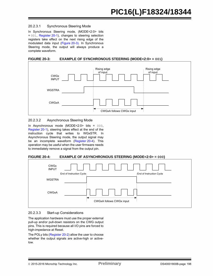
PIC16(L)F18324/18344
20.2.3.1 Synchronous Steering Mode
In Synchronous Steering mode, (MODE<2:0> bits= 001, Register 20-1), changes to steering selectionregisters take effect on the next rising edge of themodulated data input (Figure 20-3). In SynchronousSteering mode, the output will always produce acomplete waveform.
FIGURE 20-3: EXAMPLE OF SYNCHRONOUS STEERING (MODE<2:0> = 001)
20.2.3.2 Asynchronous Steering Mode
In Asynchronous mode (MODE<2:0> bits = 000,Register 20-1), steering takes effect at the end of theinstruction cycle that writes to WGxSTR. InAsynchronous Steering mode, the output signal maybe an incomplete waveform (Register 20-4). Thisoperation may be useful when the user firmware needsto immediately remove a signal from the output pin.
FIGURE 20-4: EXAMPLE OF ASYNCHRONOUS STEERING (MODE<2:0> = 000)
20.2.3.3 Start-up Considerations
The application hardware must use the proper externalpull-up and/or pull-down resistors on the CWG outputpins. This is required because all I/O pins are forced tohigh-impedance at Reset.
The POLy bits (Register 20-2) allow the user to choosewhether the output signals are active-high or active-low.
Rising edge of input
Rising edge of input
CWG A follows CWG input
CWGINPUT
CWG A
WGSTRA
CWGINPUT
CWG A
WGSTRA
End of Instruction Cycle End of Instruction Cycle
CWG A follows CWG input
2015-2016 Microchip Technology Inc. Preliminary DS40001800B-page 198
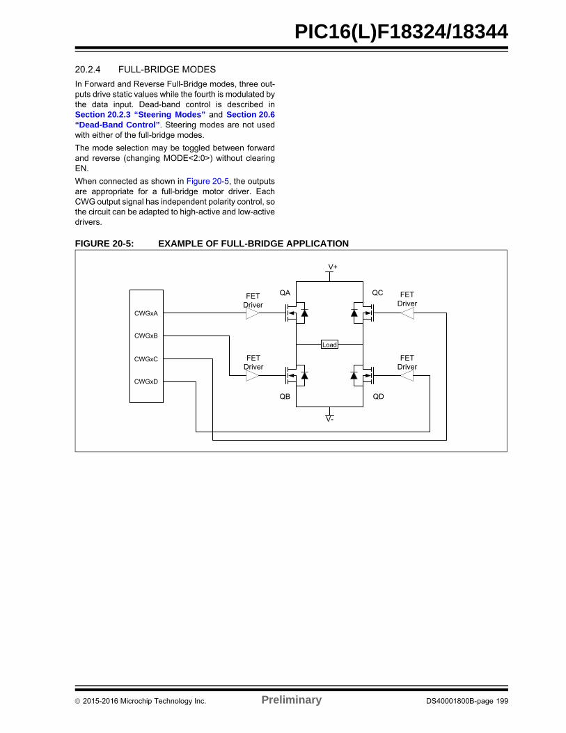
PIC16(L)F18324/18344
20.2.4 FULL-BRIDGE MODES
In Forward and Reverse Full-Bridge modes, three out-puts drive static values while the fourth is modulated bythe data input. Dead-band control is described inSection 20.2.3 “Steering Modes” and Section 20.6“Dead-Band Control”. Steering modes are not usedwith either of the full-bridge modes.
The mode selection may be toggled between forwardand reverse (changing MODE<2:0>) without clearingEN.
When connected as shown in Figure 20-5, the outputsare appropriate for a full-bridge motor driver. EachCWG output signal has independent polarity control, sothe circuit can be adapted to high-active and low-activedrivers.
FIGURE 20-5: EXAMPLE OF FULL-BRIDGE APPLICATION
V+
V-
FETDriver
FETDriver
FETDriver
FETDriver
CWG A
CWG B
CWG C
CWG D
Load
QA
QB
QC
QD
2015-2016 Microchip Technology Inc. Preliminary DS40001800B-page 199
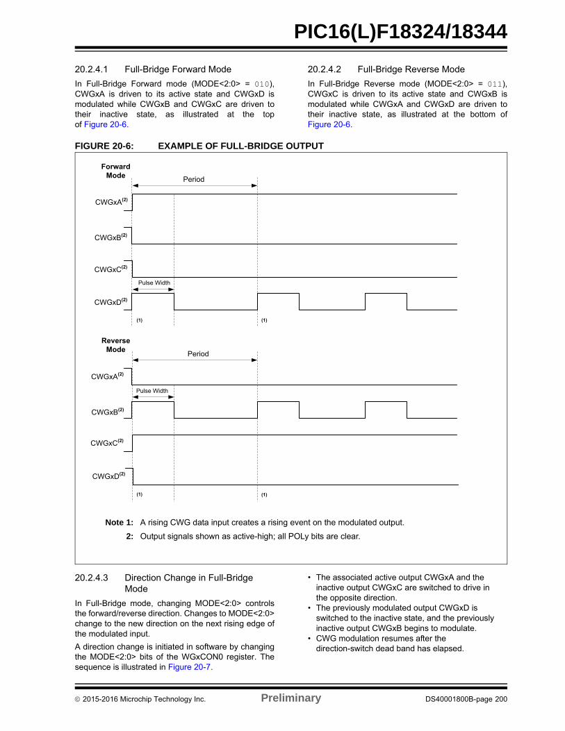
PIC16(L)F18324/18344
20.2.4.1 Full-Bridge Forward Mode
In Full-Bridge Forward mode (MODE<2:0> = 010),CWGxA is driven to its active state and CWGxD ismodulated while CWGxB and CWGxC are driven totheir inactive state, as illustrated at the topof Figure 20-6.
20.2.4.2 Full-Bridge Reverse Mode
In Full-Bridge Reverse mode (MODE<2:0> = 011),CWGxC is driven to its active state and CWGxB ismodulated while CWGxA and CWGxD are driven totheir inactive state, as illustrated at the bottom ofFigure 20-6.
FIGURE 20-6: EXAMPLE OF FULL-BRIDGE OUTPUT
20.2.4.3 Direction Change in Full-Bridge Mode
In Full-Bridge mode, changing MODE<2:0> controlsthe forward/reverse direction. Changes to MODE<2:0>change to the new direction on the next rising edge ofthe modulated input.
A direction change is initiated in software by changingthe MODE<2:0> bits of the WGxCON0 register. Thesequence is illustrated in Figure 20-7.
• The associated active output CWGxA and the inactive output CWGxC are switched to drive in the opposite direction.
• The previously modulated output CWGxD is switched to the inactive state, and the previously inactive output CWGxB begins to modulate.
• CWG modulation resumes after the direction-switch dead band has elapsed.
Note 1: A rising CWG data input creates a rising event on the modulated output.
2: Output signals shown as active-high; all POLy bits are clear.
CWG A(2)
CWG B(2)
CWG C(2)
CWG D(2)
Period
Pulse Width
(1) (1)
ForwardMode
Pulse Width
Period
Reverse Mode
CWG A(2)
CWG B(2)
CWG C(2)
CWG D(2)
(1) (1)
2015-2016 Microchip Technology Inc. Preliminary DS40001800B-page 200
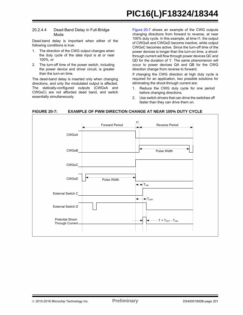
PIC16(L)F18324/18344
20.2.4.4 Dead-Band Delay in Full-Bridge Mode
Dead-band delay is important when either of thefollowing conditions is true:
1. The direction of the CWG output changes whenthe duty cycle of the data input is at or near100%, or
2. The turn-off time of the power switch, includingthe power device and driver circuit, is greaterthan the turn-on time.
The dead-band delay is inserted only when changingdirections, and only the modulated output is affected.The statically-configured outputs (CWGxA andCWGxC) are not afforded dead band, and switchessentially simultaneously.
Figure 20-7 shows an example of the CWG outputschanging directions from forward to reverse, at near100% duty cycle. In this example, at time t1, the outputof CWGxA and CWGxD become inactive, while outputCWGxC becomes active. Since the turn-off time of thepower devices is longer than the turn-on time, a shoot-through current will flow through power devices QC andQD for the duration of ‘t’. The same phenomenon willoccur to power devices QA and QB for the CWGdirection change from reverse to forward.
If changing the CWG direction at high duty cycle isrequired for an application, two possible solutions foreliminating the shoot-through current are:
1. Reduce the CWG duty cycle for one periodbefore changing directions.
2. Use switch drivers that can drive the switches offfaster than they can drive them on.
FIGURE 20-7: EXAMPLE OF PWM DIRECTION CHANGE AT NEAR 100% DUTY CYCLE
Forward Period Reverse Periodt1
Pulse Width
Pulse Width
TON
TOFF
T = TOFF - TON
CWG A
CWG B
CWG C
CWG D
External Switch C
External Switch D
Potential Shoot-Through Current
2015-2016 Microchip Technology Inc. Preliminary DS40001800B-page 201
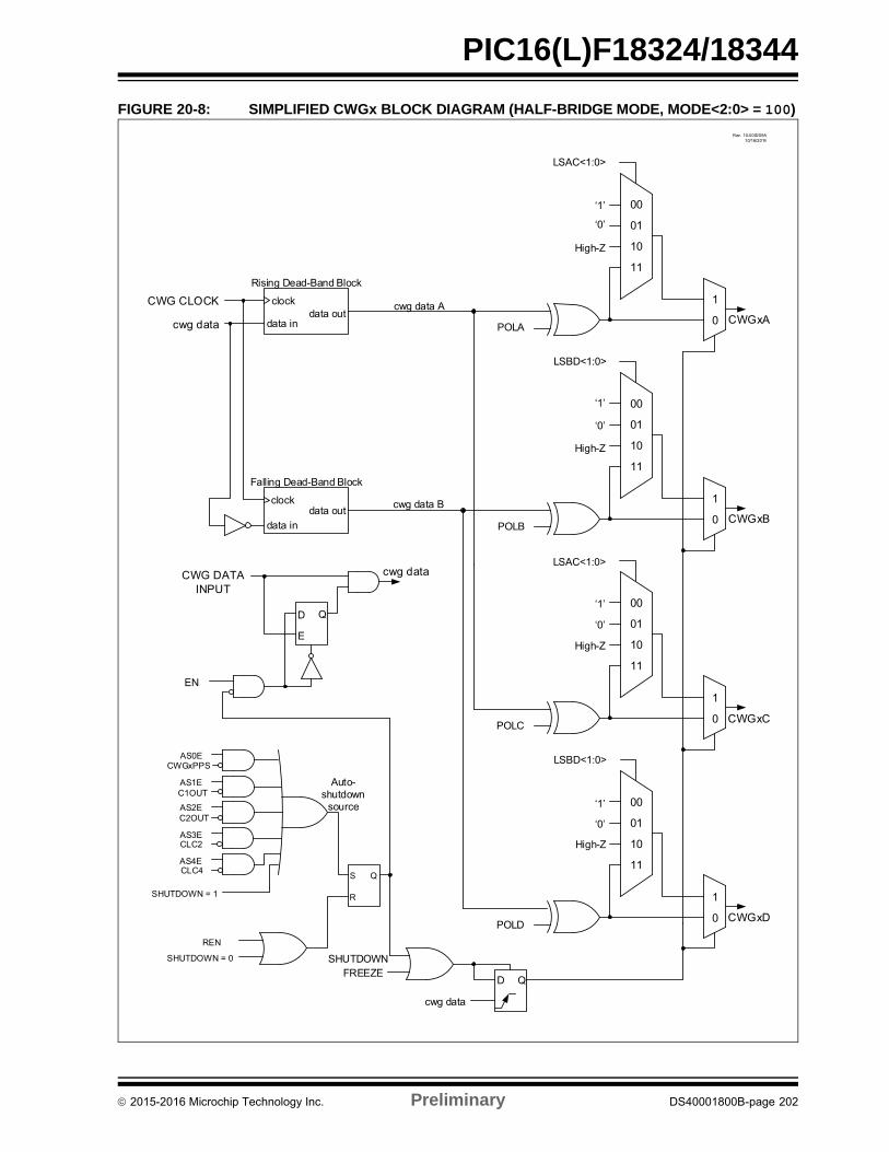
PIC16(L)F18324/18344
FIGURE 20-8: SIMPLIFIED CWGx BLOCK DIAGRAM (HALF-BRIDGE MODE, MODE<2:0> = 100)
Rev. 10-000209A10/16/2014
1
0
1
0
1
0
1
0
00
11
10
01
00
11
10
01
00
11
10
01
00
11
10
01
LSAC<1:0>
LSBD<1:0>
LSAC<1:0>
LSBD<1:0>
clock
data indata out
clock
data indata out
E
D Q
AS0E
C1OUTAS1E
AS2EC2OUT
CLC2AS3E
SHUTDOWN = 1
REN
SHUTDOWN = 0
S
R
Q
POLA
POLB
POLC
POLD
cwg data
FREEZED Q
cwg data
CWGxD
CWGxC
CWGxB
CWGxA
‘1’
‘1’
‘0’
‘1’
‘1’
‘0’
‘0’
‘0’
High-Z
High-Z
High-Z
High-Z
Rising Dead-Band Block
Falling Dead-Band Block
cwg data A
cwg data B
EN
Auto-shutdown
source
SHUTDOWN
CWGxPPS
CLC4AS4E
CWG DATA INPUT
CWG CLOCK
cwg data
2015-2016 Microchip Technology Inc. Preliminary DS40001800B-page 202
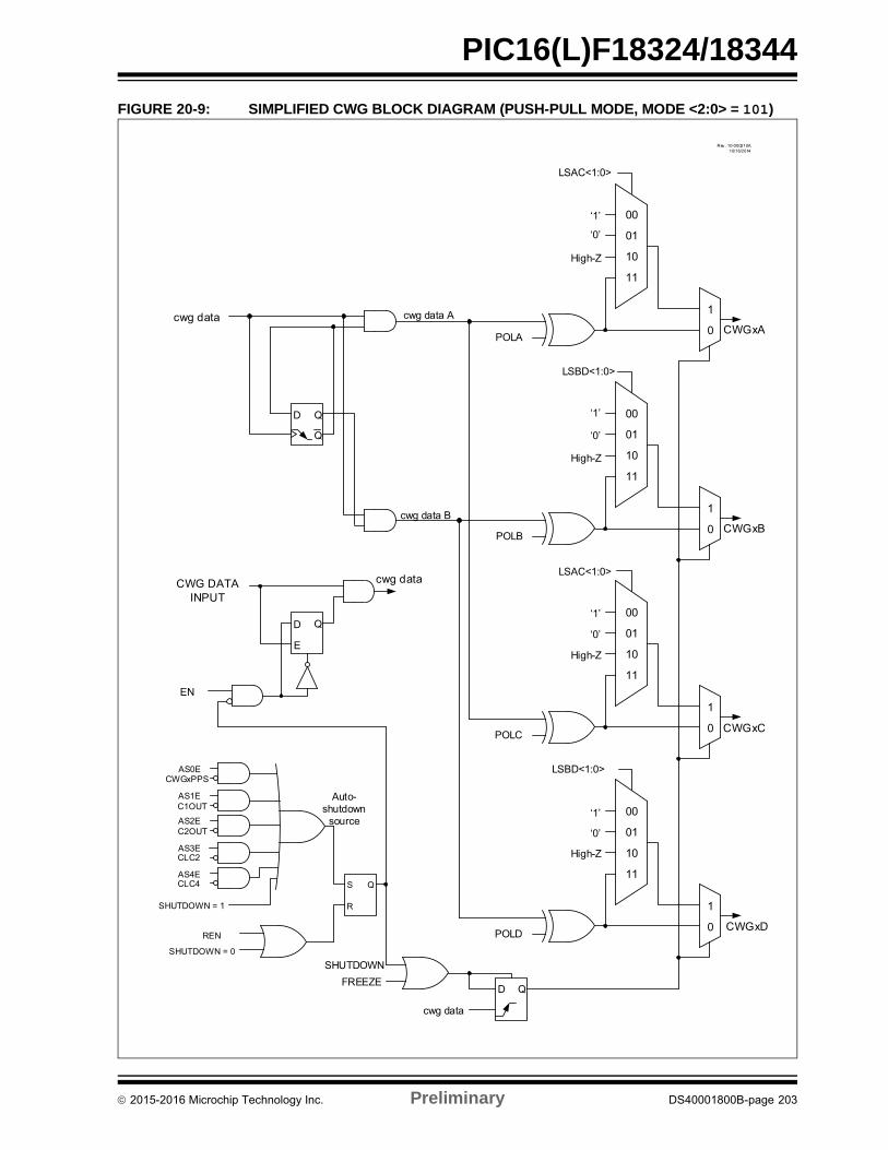
PIC16(L)F18324/18344
FIGURE 20-9: SIMPLIFIED CWG BLOCK DIAGRAM (PUSH-PULL MODE, MODE <2:0> = 101)
Rev. 10-000210A10/16/2014
1
0
1
0
1
0
1
0
00
11
10
01
00
11
10
01
00
11
10
01
00
11
10
01
LSAC<1:0>
LSBD<1:0>
LSAC<1:0>
LSBD<1:0>
cwg data
CWG DATA INPUT
E
D Q
SHUTDOWN = 1
REN
SHUTDOWN = 0
S
R
Q
POLA
POLB
POLC
POLD
cwg data
FREEZED Q
cwg data
CWGxD
CWGxC
CWGxB
CWGxA
‘1’
‘1’
‘0’
‘1’
‘1’
‘0’
‘0’
‘0’
High-Z
High-Z
High-Z
High-Z
D Q
Q
cwg data A
cwg data B
EN
Auto-shutdown
source
SHUTDOWN
AS0E
C1OUTAS1E
AS2EC2OUT
CLC2AS3E
CWGxPPS
CLC4AS4E
2015-2016 Microchip Technology Inc. Preliminary DS40001800B-page 203
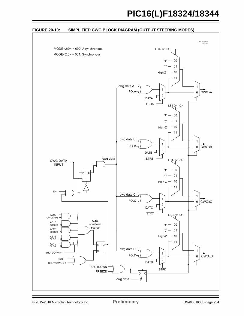
PIC16(L)F18324/18344
FIGURE 20-10: SIMPLIFIED CWG BLOCK DIAGRAM (OUTPUT STEERING MODES)
Rev. 10-000211A10/16/2014
1
0
1
0
1
0
1
0
00
11
10
01
00
11
10
01
00
11
10
01
00
11
10
01
LSAC<1:0>
LSBD<1:0>
LSAC<1:0>
LSBD<1:0>
CWG DATA INPUT
E
D Q
SHUTDOWN = 1
REN
SHUTDOWN = 0
S
R
Q
POLA
POLB
POLC
POLD
cwg data
FREEZED Q
CWGxD
CWGxC
CWGxB
CWGxA
‘1’
‘1’
‘0’
‘1’
‘1’
‘0’
‘0’
‘0’
High-Z
High-Z
High-Z
High-Z
1
0DATD
STRD
1
0DATC
STRC
1
0DATB
STRB
1
0DATA
STRA
cwg data
SHUTDOWN
Auto-shutdown
source
cwg data D
cwg data C
cwg data B
cwg data A
EN
MODE<2:0> = 000: Asynchronous
MODE<2:0> = 001: Synchronous
AS0E
C1OUTAS1E
AS2EC2OUT
CLC2AS3E
CWGxPPS
CLC4AS4E
2015-2016 Microchip Technology Inc. Preliminary DS40001800B-page 204
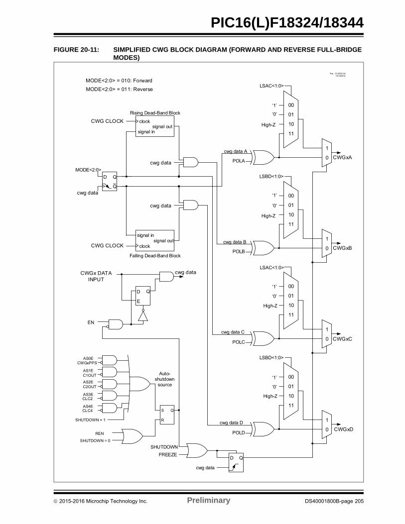
PIC16(L)F18324/18344
FIGURE 20-11: SIMPLIFIED CWG BLOCK DIAGRAM (FORWARD AND REVERSE FULL-BRIDGE MODES)
Rev. 10-000212A10/16/2014
1
0
1
0
1
0
1
0
00
11
10
01
00
11
10
01
00
11
10
01
00
11
10
01
LSAC<1:0>
LSBD<1:0>
LSAC<1:0>
LSBD<1:0>
cwg data
CWG CLOCK clock
signal insignal out
clock
signal insignal out
CWGx DATA INPUT
E
D Q
SHUTDOWN = 1
REN
SHUTDOWN = 0
S
R
Q
POLA
POLB
POLC
POLD
cwg data
FREEZED Q
cwg data
CWGxD
CWGxC
CWGxB
CWGxA
‘1’
‘1’
‘0’
‘1’
‘1’
‘0’
‘0’
‘0’
High-Z
High-Z
High-Z
High-Z
Rising Dead-Band Block
Falling Dead-Band Block
cwg data A
cwg data B
EN
Auto-shutdown
source
SHUTDOWN
MODE<2:0> = 010: Forward
MODE<2:0> = 011: Reverse
CWG CLOCK
MODE<2:0>cwg data
cwg data
cwg data C
cwg data D
D Q
Q
AS0E
C1OUTAS1E
AS2EC2OUT
CLC2AS3E
CWGxPPS
CLC4AS4E
2015-2016 Microchip Technology Inc. Preliminary DS40001800B-page 205
PIC16(L)F18324/18344
20.3 Clock Source
The clock source is used to drive the dead-band timingcircuits. The CWGx module allows the following clocksources to be selected:
• FOSC (system clock)• HFINTOSC (16 MHz only)
When the HFINTOSC is selected the HFINTOSC willbe kept running during Sleep. Therefore, CWG modesrequiring dead band can operate in Sleep provided thatthe CWG data input is also active during Sleep. Theclock sources are selected using the CS bit of theCWGxCLKCON register (Register 20-3).
20.4 Selectable Input Sources
The CWG generates the output waveforms from theinput sources in Table 20-1.
The input sources are selected using the DAT<3:0>bits in the CWGxDAT register (Register 20-4).
20.5 Output Control
Immediately after the CWG module is enabled, thecomplementary drive is configured with all outputdrives cleared.
20.5.1 CWGx OUTPUTS
Each CWG output can be routed to a Peripheral PinSelect (PPS) output via the RxyPPS register (seeSection 13.0 “Peripheral Pin Select (PPS)Module”).
20.5.2 POLARITY CONTROL
The polarity of each CWG output can be selectedindependently. When the output polarity bit is set, thecorresponding output is active-low. Clearing the outputpolarity bit configures the corresponding output asactive-high. However, polarity does not affect theoverride levels. Output polarity is selected with thePOLy bits of the CWGxCON1 register.
20.6 Dead-Band Control
Dead-band control provides for non-overlapping outputsignals to prevent current shoot-through in powerswitches. The CWGx modules contain two 6-bitdead-band counters. These counters can be loadedwith values that will determine the length of the deadband initiated on either the rising or falling edges of theinput source. Dead-band control is used in either Half-Bridge or Full-Bridge modes.
The rising-edge dead-band delay is determined by therising dead-band count register (Register 20-8,CWGxDBR) and the falling-edge dead-band delay isdetermined by the falling dead-band count register(Register 20-9, CWGxDBF). Dead-band duration isestablished by counting the CWG clock periods fromzero up to the value loaded into either the rising or fall-ing dead-band counter registers. The dead-bandcounters are incremented on every rising edge of theCWG clock source.
20.6.1 RISING EDGE AND REVERSE DEAD BAND
In Half-Bridge mode, the rising edge dead band delaysthe turn-on of the CWGxA output after the rising edgeof the CWG data input. In Full-Bridge mode, thereverse dead-band delay is only inserted whenchanging directions from Forward mode to Reversemode, and only the modulated output CWGxB isaffected.
The CWGxDBR register determines the duration of thedead-band interval on the rising edge of the inputsource signal. This duration is from 0 to 64 periods ofthe CWG clock.
Dead band is always initiated on the edge of the inputsource signal. A count of zero indicates that no deadband is present.
If the input source signal reverses polarity before thedead-band count is completed then no output will beseen on the respective output.
The CWGxDBR register value is double-buffered. IfEN = 0 (Register 20-1), the buffer is loaded whenCWGxDBR is written. If EN = 1, then the buffer will beloaded at the rising edge, following the first falling edgeof the data input after the LD bit (Register 20-1) is set.
TABLE 20-1: SELECTABLE INPUT SOURCES
Source Peripheral
Description
CWGxPPS CWG PPS input connection
C1OUT Comparator 1 output
C2OUT Comparator 2 output
CCP1 Capture/Compare/PWM output
CCP2 Capture/Compare/PWM output
CCP3 Capture/Compare/PWM output
CCP4 Capture/Compare/PWM output
PWM5 PWM5 output
PWM6 PWM6 output
NCO1 Numerically Controlled Oscillator (NCO) output
CLC1 Configurable Logic Cell 1 output
CLC2 Configurable Logic Cell 2 output
CLC3 Configurable Logic Cell 3 output
CLC3 Configurable Logic Cell 4 output
2015-2016 Microchip Technology Inc. Preliminary DS40001800B-page 206
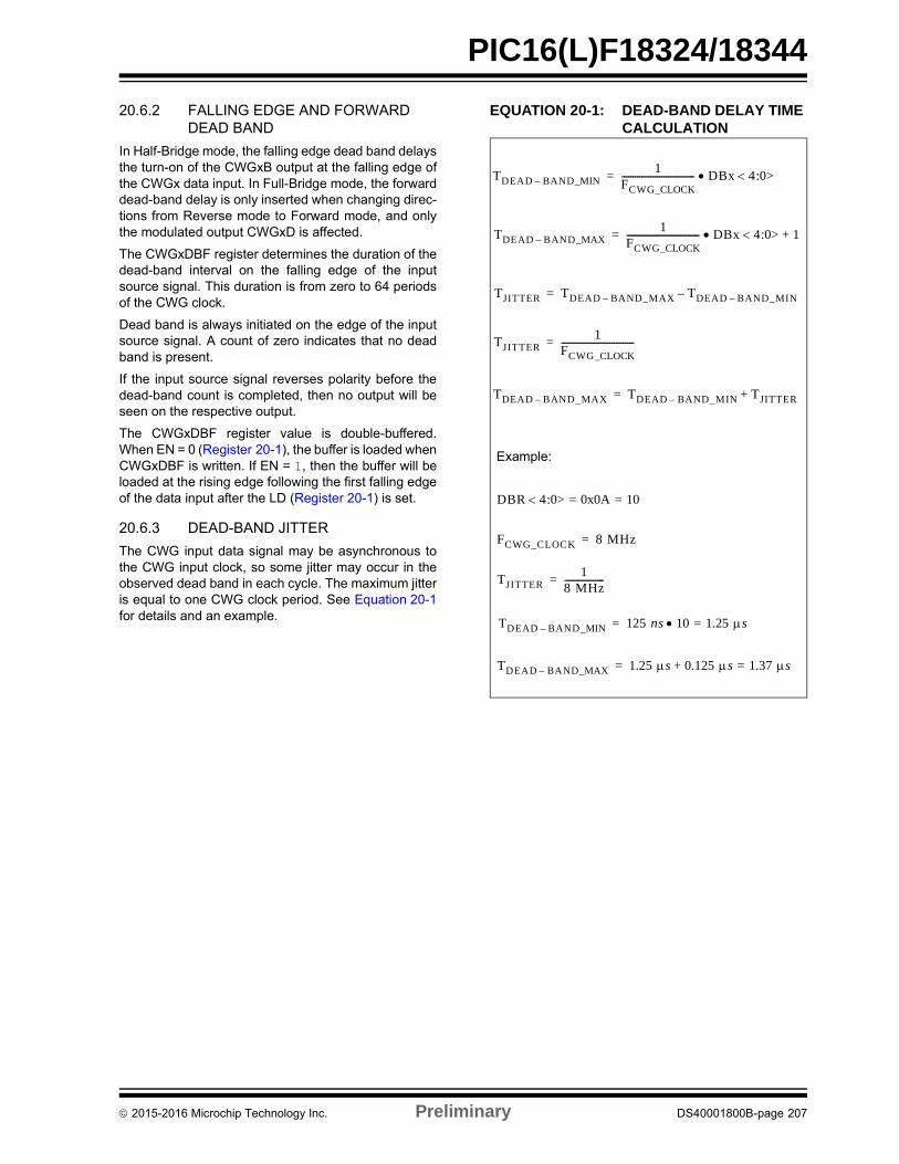
PIC16(L)F18324/18344
20.6.2 FALLING EDGE AND FORWARD DEAD BAND
In Half-Bridge mode, the falling edge dead band delaysthe turn-on of the CWGxB output at the falling edge ofthe CWGx data input. In Full-Bridge mode, the forwarddead-band delay is only inserted when changing direc-tions from Reverse mode to Forward mode, and onlythe modulated output CWGxD is affected.
The CWGxDBF register determines the duration of thedead-band interval on the falling edge of the inputsource signal. This duration is from zero to 64 periodsof the CWG clock.
Dead band is always initiated on the edge of the inputsource signal. A count of zero indicates that no deadband is present.
If the input source signal reverses polarity before thedead-band count is completed, then no output will beseen on the respective output.
The CWGxDBF register value is double-buffered.When EN = 0 (Register 20-1), the buffer is loaded whenCWGxDBF is written. If EN = 1, then the buffer will beloaded at the rising edge following the first falling edgeof the data input after the LD (Register 20-1) is set.
20.6.3 DEAD-BAND JITTER
The CWG input data signal may be asynchronous tothe CWG input clock, so some jitter may occur in theobserved dead band in each cycle. The maximum jitteris equal to one CWG clock period. See Equation 20-1for details and an example.
EQUATION 20-1: DEAD-BAND DELAY TIME CALCULATION
TDEAD BAND_MIN–1
FCWG_CLOCK--------------------------------- DBx 4:0>=
TDEAD BAND_MAX–1
FCWG_CLOCK--------------------------------- DBx 4:0> 1+=
TJITTER TDEAD BAND_MAX– TDEAD BAND_MIN––=
TJITTER1
FCWG_CLOCK---------------------------------=
TDEAD BAND_MAX– TDEAD BAND_MIN– TJITTER+=
Example:
DBR 4:0> 0x0A 10= =
FCWG_CLOCK 8 MHz=
TJITTER1
8 MHz------------------=
TDEAD BAND_MIN– 125 ns 10 1.25 s==
TDEAD BAND_MAX– 1.25 s 0.125 s 1.37 s=+=
2015-2016 Microchip Technology Inc. Preliminary DS40001800B-page 207
PIC16(L)F18324/18344
20.7 Auto-Shutdown Control
Auto-shutdown is a method to immediately override theCWG output levels with specific overrides that allow forsafe shutdown of the circuit. The shutdown state canbe either cleared automatically or held until cleared bysoftware.
20.7.1 SHUTDOWN
The shutdown state can be entered by either of thefollowing two methods:
• Software generated• External input
The SHUTDOWN bit indicates when a Shutdowncondition exists. The bit may be set or cleared insoftware or by hardware.
20.7.1.1 Software-Generated Shutdown
Setting the SHUTDOWN bit of the CWGxAS0 registerwill force the CWG into the shutdown state.
When auto-restart is disabled, the shutdown state willpersist as long as the SHUTDOWN bit is set.
When auto-restart is enabled, the SHUTDOWN bit willclear automatically and resume operation on the nextrising edge event.
20.7.1.2 External Input Source Shutdown
Any of the auto-shutdown external inputs can beselected to suspend the CWG operation. Thesesources are individually enabled by the ASxE bits of theCWGxAS1 register (Register 20-7). When any of theselected inputs goes active (pins are active-low), theCWG outputs will immediately switch to the overridelevels selected by the LSBD<1:0> and LSAC<1:0> bitswithout any software delay (Section 20.7.1.3 “PinOverride Levels”). Any of the following external inputsources can be selected to cause a Shutdowncondition:
• Comparator C1• Comparator C2• CLC2• CWGxPPS
20.7.1.3 Pin Override Levels
The levels driven to the CWG outputs during an auto-shutdown event are controlled by the LSBD<1:0> andLSAC<1:0> bits of the CWGxAS0 register(Register 20-6). The LSBD<1:0> bits control CWGxB/Doutput levels, while the LSAC<1:0> bits control theCWGxA/C output levels.
20.7.1.4 Auto-Shutdown Interrupts
When an auto-shutdown event occurs, either bysoftware or hardware setting SHUTDOWN, the CWGxIFflag bit of the PIR4 register is set (Register 8-11).
20.8 Auto-Shutdown Restart
After an auto-shutdown event has occurred, there aretwo ways to resume operation:
• Software controlled• Auto-restart
In either case, the shut-down source must be clearedbefore the restart can take place. That is, either theShutdown condition must be removed, or thecorresponding WGASxE bit must be cleared.
20.8.1 SOFTWARE-CONTROLLED RESTART
If the REN bit of the CWGxASD0 register is clear(REN = 0), the CWGx module must be restarted afteran auto-shutdown event through software.
Once all Auto-Shutdown conditions are removed, thesoftware must clear SHUTDOWN. Once SHUTDOWNis cleared, the CWG module will resume operationupon the first rising edge of the CWG data input.
20.8.2 AUTO-RESTART
If the REN bit of the CWGxASD0 register is set(REN = 1), the CWGx module will restart from the shut-down state automatically.
Once all Auto-Shutdown conditions are removed, thehardware will automatically clear SHUTDOWN. OnceSHUTDOWN is cleared, the CWG module will resumeoperation upon the first rising edge of the CWG datainput.
Note: Shutdown inputs are level sensitive, notedge sensitive. The shutdown statecannot be cleared, except by disablingauto-shutdown, as long as the shutdowninput level persists.
Note: SHUTDOWN bit cannot be cleared insoftware if the auto-shutdown condition isstill present.
Note: SHUTDOWN bit cannot be cleared insoftware if the auto-shutdown condition isstill present.
2015-2016 Microchip Technology Inc. Preliminary DS40001800B-page 208
PIC16(L)F18324/18344
20.9 Operation During Sleep
The CWGx module will operate during Sleep, providedthat the input sources remain active.
If the HFINTOSC is selected as the module clocksource, dead-band generation will remain active. Thiswill have a direct effect on the Sleep mode current.
20.10 Configuring the CWG
1. Ensure that the TRIS control bits correspondingto CWG outputs are set so that all areconfigured as inputs, ensuring that the outputsare inactive during setup. External hardwareshould ensure that pin levels are held to safelevels.
2. Clear the EN bit, if not already cleared.3. Configure the MODE<2:0> bits of the
CWGxCON0 register to set the output operatingmode.
4. Configure the POLy bits of the CWGxCON1register to set the output polarities.
5. Configure the DAT<3:0> bits of the CWGxDATregister to select the data input source.
6. If a Steering mode is selected, configure theSTRy bits to select the desired output on theCWG outputs.
7. Configure the LSBD<1:0> and LSAC<1:0> bitsof the CWGxAS0 register to select the auto-shutdown output override states (this isnecessary even if not using auto-shutdownbecause start-up will be from a shutdown state).
8. If auto-restart is desired, set the REN bit ofCWGxAS0.
9. If auto-shutdown is desired, configure the ASxEbits of the CWGxAS1 register to select theshutdown source.
10. Set the desired rising and falling dead-bandtimes with the CWGxDBR and CWGxDBFregisters.
11. Select the clock source in the CWGxCLKCONregister.
12. Set the EN bit to enable the module.13. Clear the TRIS bits that correspond to the CWG
outputs to set them as outputs.14. If auto-restart is to be used, set the REN bit and
the SHUTDOWN bit will be clearedautomatically. Otherwise, clear theSHUTDOWN bit in software to start the CWG.
2015-2016 Microchip Technology Inc. Preliminary DS40001800B-page 209
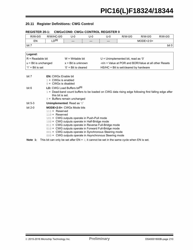
PIC16(L)F18324/18344
20.11 Register Definitions: CWG Control
REGISTER 20-1: CWGxCON0: CWGx CONTROL REGISTER 0
R/W-0/0 R/W/HC-0/0 U-0 U-0 U-0 R/W-0/0 R/W-0/0 R/W-0/0
EN LD(1) — — — MODE<2:0>
bit 7 bit 0
Legend:
R = Readable bit W = Writable bit U = Unimplemented bit, read as ‘0’
u = Bit is unchanged x = Bit is unknown -n/n = Value at POR and BOR/Value at all other Resets
‘1’ = Bit is set ‘0’ = Bit is cleared HS/HC = Bit is set/cleared by hardware
bit 7 EN: CWGx Enable bit1 = CWGx is enabled0 = CWGx is disabled
bit 6 LD: CWG Load Buffers bit(1)
1 = Dead-band count buffers to be loaded on CWG data rising edge following first falling edge afterthis bit is set.
0 = Buffers remain unchanged
bit 5-3 Unimplemented: Read as ‘0’
bit 2-0 MODE<2:0>: CWGx Mode bits111 = Reserved110 = Reserved101 = CWG outputs operate in Push-Pull mode100 = CWG outputs operate in Half-Bridge mode011 = CWG outputs operate in Reverse Full-Bridge mode010 = CWG outputs operate in Forward Full-Bridge mode001 = CWG outputs operate in Synchronous Steering mode000 = CWG outputs operate in Asynchronous Steering mode
Note 1: This bit can only be set after EN = 1; it cannot be set in the same cycle when EN is set.
2015-2016 Microchip Technology Inc. Preliminary DS40001800B-page 210
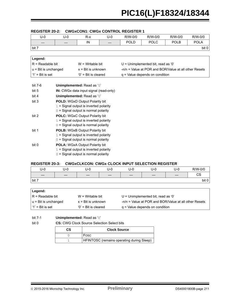
PIC16(L)F18324/18344
REGISTER 20-2: CWGxCON1: CWGx CONTROL REGISTER 1
U-0 U-0 R-x U-0 R/W-0/0 R/W-0/0 R/W-0/0 R/W-0/0
— — IN — POLD POLC POLB POLA
bit 7 bit 0
Legend:
R = Readable bit W = Writable bit U = Unimplemented bit, read as ‘0’
u = Bit is unchanged x = Bit is unknown -n/n = Value at POR and BOR/Value at all other Resets
‘1’ = Bit is set ‘0’ = Bit is cleared q = Value depends on condition
bit 7-6 Unimplemented: Read as ‘0’
bit 5 IN: CWGx data input signal (read-only)
bit 4 Unimplemented: Read as ‘0’
bit 3 POLD: WGxD Output Polarity bit1 = Signal output is inverted polarity0 = Signal output is normal polarity
bit 2 POLC: WGxC Output Polarity bit1 = Signal output is inverted polarity0 = Signal output is normal polarity
bit 1 POLB: WGxB Output Polarity bit1 = Signal output is inverted polarity0 = Signal output is normal polarity
bit 0 POLA: WGxA Output Polarity bit1 = Signal output is inverted polarity0 = Signal output is normal polarity
REGISTER 20-3: CWGxCLKCON: CWGx CLOCK INPUT SELECTION REGISTER
U-0 U-0 U-0 U-0 U-0 U-0 U-0 R/W-0/0
— — — — — — — CS
bit 7 bit 0
Legend:
R = Readable bit W = Writable bit U = Unimplemented bit, read as ‘0’
u = Bit is unchanged x = Bit is unknown -n/n = Value at POR and BOR/Value at all other Resets
‘1’ = Bit is set ‘0’ = Bit is cleared q = Value depends on condition
bit 7-1 Unimplemented: Read as ‘0’
bit 0 CS: CWG Clock Source Selection Select bits
CS Clock Source
0 FOSC
1 HFINTOSC (remains operating during Sleep)
2015-2016 Microchip Technology Inc. Preliminary DS40001800B-page 211
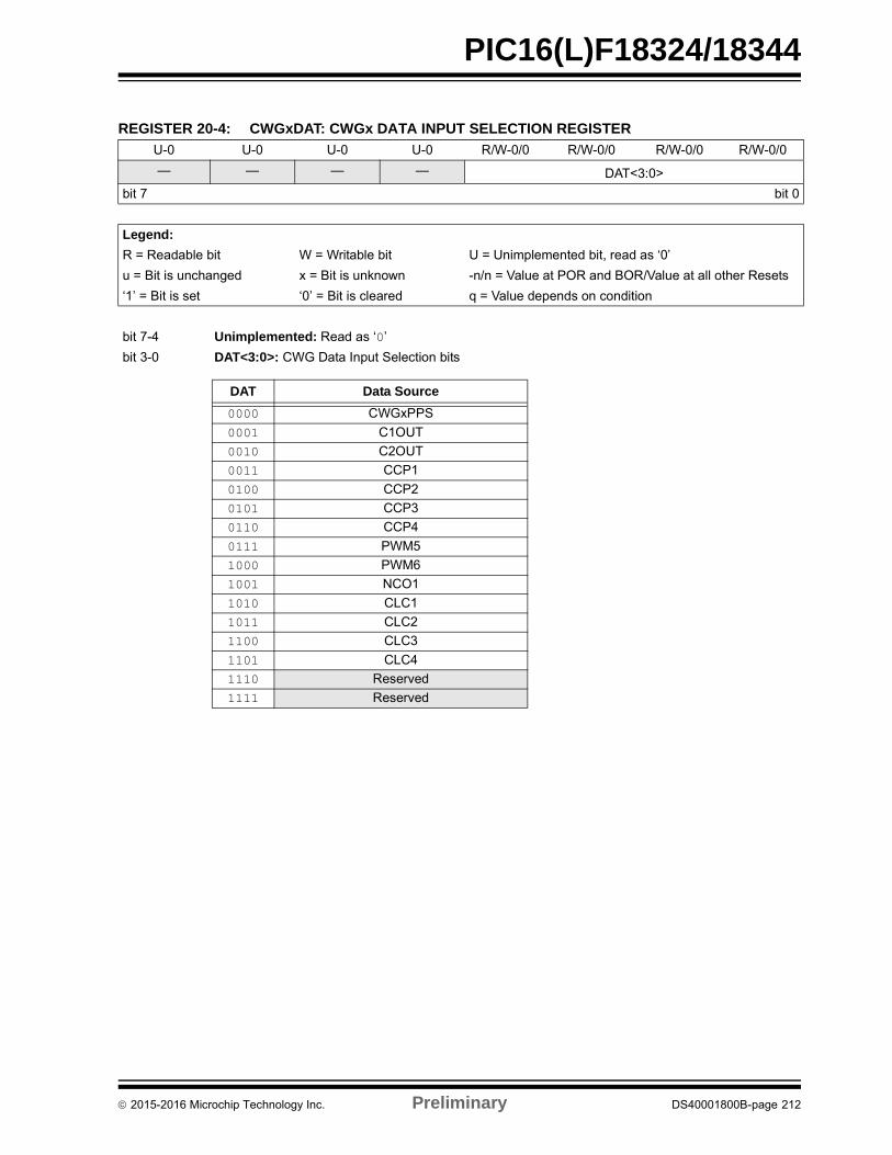
PIC16(L)F18324/18344
REGISTER 20-4: CWGxDAT: CWGx DATA INPUT SELECTION REGISTER
U-0 U-0 U-0 U-0 R/W-0/0 R/W-0/0 R/W-0/0 R/W-0/0
— — — — DAT<3:0>
bit 7 bit 0
Legend:
R = Readable bit W = Writable bit U = Unimplemented bit, read as ‘0’
u = Bit is unchanged x = Bit is unknown -n/n = Value at POR and BOR/Value at all other Resets
‘1’ = Bit is set ‘0’ = Bit is cleared q = Value depends on condition
bit 7-4 Unimplemented: Read as ‘0’
bit 3-0 DAT<3:0>: CWG Data Input Selection bits
DAT Data Source
0000 CWGxPPS
0001 C1OUT
0010 C2OUT
0011 CCP1
0100 CCP2
0101 CCP3
0110 CCP4
0111 PWM5
1000 PWM6
1001 NCO1
1010 CLC1
1011 CLC2
1100 CLC3
1101 CLC4
1110 Reserved
1111 Reserved
2015-2016 Microchip Technology Inc. Preliminary DS40001800B-page 212
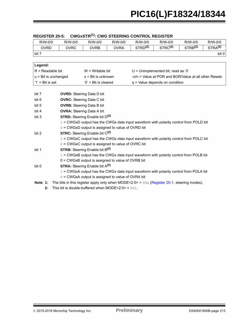
PIC16(L)F18324/18344
REGISTER 20-5: CWGxSTR(1): CWG STEERING CONTROL REGISTER
R/W-0/0 R/W-0/0 R/W-0/0 R/W-0/0 R/W-0/0 R/W-0/0 R/W-0/0 R/W-0/0
OVRD OVRC OVRB OVRA STRD(2) STRC(2) STRB(2) STRA(2)
bit 7 bit 0
Legend:
R = Readable bit W = Writable bit U = Unimplemented bit, read as ‘0’
u = Bit is unchanged x = Bit is unknown -n/n = Value at POR and BOR/Value at all other Resets
‘1’ = Bit is set ‘0’ = Bit is cleared q = Value depends on condition
bit 7 OVRD: Steering Data D bit
bit 6 OVRC: Steering Data C bit
bit 5 OVRB: Steering Data B bit
bit 4 OVRA: Steering Data A bit
bit 3 STRD: Steering Enable bit D(2)
1 = CWGxD output has the CWGx data input waveform with polarity control from POLD bit
0 = CWGxD output is assigned to value of OVRD bit
bit 2 STRC: Steering Enable bit C(2)
1 = CWGxC output has the CWGx data input waveform with polarity control from POLC bit
0 = CWGxC output is assigned to value of OVRC bit
bit 1 STRB: Steering Enable bit B(2)
1 = CWGxB output has the CWGx data input waveform with polarity control from POLB bit
0 = CWGxB output is assigned to value of OVRB bit
bit 0 STRA: Steering Enable bit A(2)
1 = CWGxA output has the CWGx data input waveform with polarity control from POLA bit
0 = CWGxA output is assigned to value of OVRA bit
Note 1: The bits in this register apply only when MODE<2:0> = 00x (Register 20-1, steering modes).
2: This bit is double-buffered when MODE<2:0> = 001.
2015-2016 Microchip Technology Inc. Preliminary DS40001800B-page 213
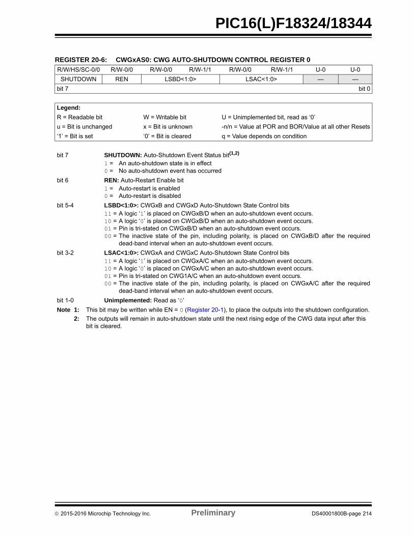
PIC16(L)F18324/18344
REGISTER 20-6: CWGxAS0: CWG AUTO-SHUTDOWN CONTROL REGISTER 0
R/W/HS/SC-0/0 R/W-0/0 R/W-0/0 R/W-1/1 R/W-0/0 R/W-1/1 U-0 U-0
SHUTDOWN REN LSBD<1:0> LSAC<1:0> — —
bit 7 bit 0
Legend:
R = Readable bit W = Writable bit U = Unimplemented bit, read as ‘0’
u = Bit is unchanged x = Bit is unknown -n/n = Value at POR and BOR/Value at all other Resets
‘1’ = Bit is set ‘0’ = Bit is cleared q = Value depends on condition
bit 7 SHUTDOWN: Auto-Shutdown Event Status bit(1,2)
1 = An auto-shutdown state is in effect0 = No auto-shutdown event has occurred
bit 6 REN: Auto-Restart Enable bit1 = Auto-restart is enabled0 = Auto-restart is disabled
bit 5-4 LSBD<1:0>: CWGxB and CWGxD Auto-Shutdown State Control bits11 = A logic ‘1’ is placed on CWGxB/D when an auto-shutdown event occurs.10 = A logic ‘0’ is placed on CWGxB/D when an auto-shutdown event occurs.01 = Pin is tri-stated on CWGxB/D when an auto-shutdown event occurs.00 = The inactive state of the pin, including polarity, is placed on CWGxB/D after the required
dead-band interval when an auto-shutdown event occurs.
bit 3-2 LSAC<1:0>: CWGxA and CWGxC Auto-Shutdown State Control bits11 = A logic ‘1’ is placed on CWGxA/C when an auto-shutdown event occurs.10 = A logic ‘0’ is placed on CWGxA/C when an auto-shutdown event occurs.01 = Pin is tri-stated on CWG1A/C when an auto-shutdown event occurs.00 = The inactive state of the pin, including polarity, is placed on CWGxA/C after the required
dead-band interval when an auto-shutdown event occurs.
bit 1-0 Unimplemented: Read as ‘0’
Note 1: This bit may be written while EN = 0 (Register 20-1), to place the outputs into the shutdown configuration.
2: The outputs will remain in auto-shutdown state until the next rising edge of the CWG data input after this bit is cleared.
2015-2016 Microchip Technology Inc. Preliminary DS40001800B-page 214
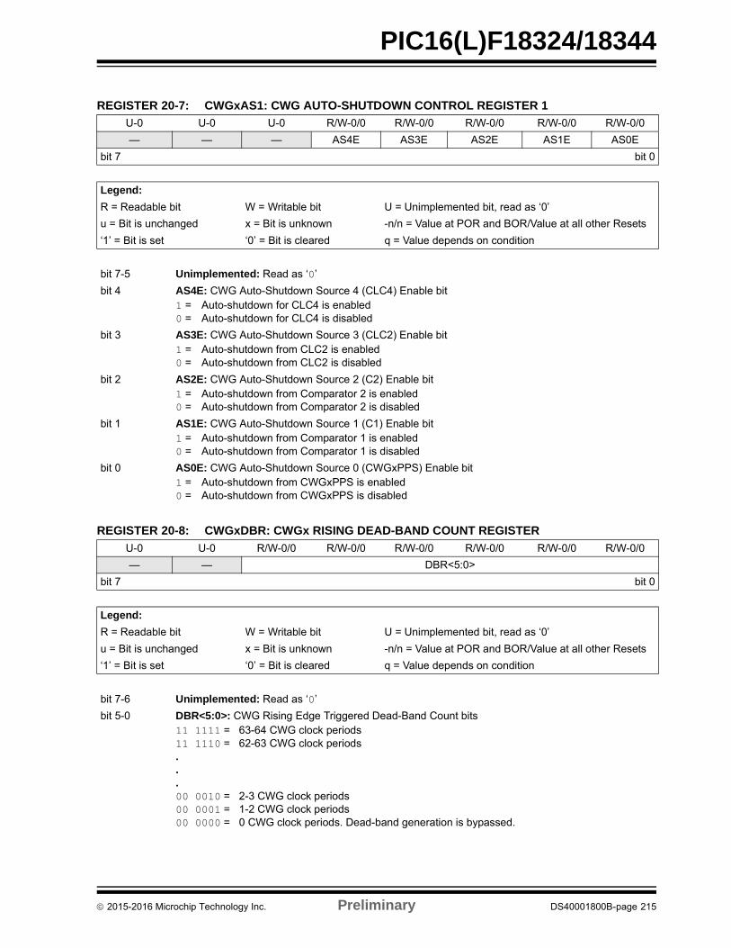
PIC16(L)F18324/18344
REGISTER 20-7: CWGxAS1: CWG AUTO-SHUTDOWN CONTROL REGISTER 1
U-0 U-0 U-0 R/W-0/0 R/W-0/0 R/W-0/0 R/W-0/0 R/W-0/0
— — — AS4E AS3E AS2E AS1E AS0E
bit 7 bit 0
Legend:
R = Readable bit W = Writable bit U = Unimplemented bit, read as ‘0’
u = Bit is unchanged x = Bit is unknown -n/n = Value at POR and BOR/Value at all other Resets
‘1’ = Bit is set ‘0’ = Bit is cleared q = Value depends on condition
bit 7-5 Unimplemented: Read as ‘0’
bit 4 AS4E: CWG Auto-Shutdown Source 4 (CLC4) Enable bit1 = Auto-shutdown for CLC4 is enabled0 = Auto-shutdown for CLC4 is disabled
bit 3 AS3E: CWG Auto-Shutdown Source 3 (CLC2) Enable bit1 = Auto-shutdown from CLC2 is enabled0 = Auto-shutdown from CLC2 is disabled
bit 2 AS2E: CWG Auto-Shutdown Source 2 (C2) Enable bit1 = Auto-shutdown from Comparator 2 is enabled0 = Auto-shutdown from Comparator 2 is disabled
bit 1 AS1E: CWG Auto-Shutdown Source 1 (C1) Enable bit1 = Auto-shutdown from Comparator 1 is enabled0 = Auto-shutdown from Comparator 1 is disabled
bit 0 AS0E: CWG Auto-Shutdown Source 0 (CWGxPPS) Enable bit1 = Auto-shutdown from CWGxPPS is enabled0 = Auto-shutdown from CWGxPPS is disabled
REGISTER 20-8: CWGxDBR: CWGx RISING DEAD-BAND COUNT REGISTER
U-0 U-0 R/W-0/0 R/W-0/0 R/W-0/0 R/W-0/0 R/W-0/0 R/W-0/0
— — DBR<5:0>
bit 7 bit 0
Legend:
R = Readable bit W = Writable bit U = Unimplemented bit, read as ‘0’
u = Bit is unchanged x = Bit is unknown -n/n = Value at POR and BOR/Value at all other Resets
‘1’ = Bit is set ‘0’ = Bit is cleared q = Value depends on condition
bit 7-6 Unimplemented: Read as ‘0’
bit 5-0 DBR<5:0>: CWG Rising Edge Triggered Dead-Band Count bits11 1111 = 63-64 CWG clock periods11 1110 = 62-63 CWG clock periods...00 0010 = 2-3 CWG clock periods00 0001 = 1-2 CWG clock periods00 0000 = 0 CWG clock periods. Dead-band generation is bypassed.
2015-2016 Microchip Technology Inc. Preliminary DS40001800B-page 215
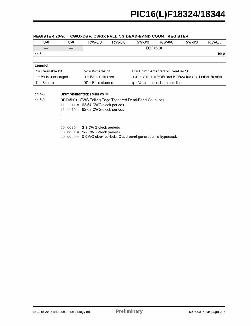
PIC16(L)F18324/18344
REGISTER 20-9: CWGxDBF: CWGx FALLING DEAD-BAND COUNT REGISTER
U-0 U-0 R/W-0/0 R/W-0/0 R/W-0/0 R/W-0/0 R/W-0/0 R/W-0/0
— — DBF<5:0>
bit 7 bit 0
Legend:
R = Readable bit W = Writable bit U = Unimplemented bit, read as ‘0’
u = Bit is unchanged x = Bit is unknown -n/n = Value at POR and BOR/Value at all other Resets
‘1’ = Bit is set ‘0’ = Bit is cleared q = Value depends on condition
bit 7-6 Unimplemented: Read as ‘0’
bit 5-0 DBF<5:0>: CWG Falling Edge Triggered Dead-Band Count bits11 1111 = 63-64 CWG clock periods11 1110 = 62-63 CWG clock periods...00 0010 = 2-3 CWG clock periods00 0001 = 1-2 CWG clock periods00 0000 = 0 CWG clock periods. Dead-band generation is bypassed.
2015-2016 Microchip Technology Inc. Preliminary DS40001800B-page 216
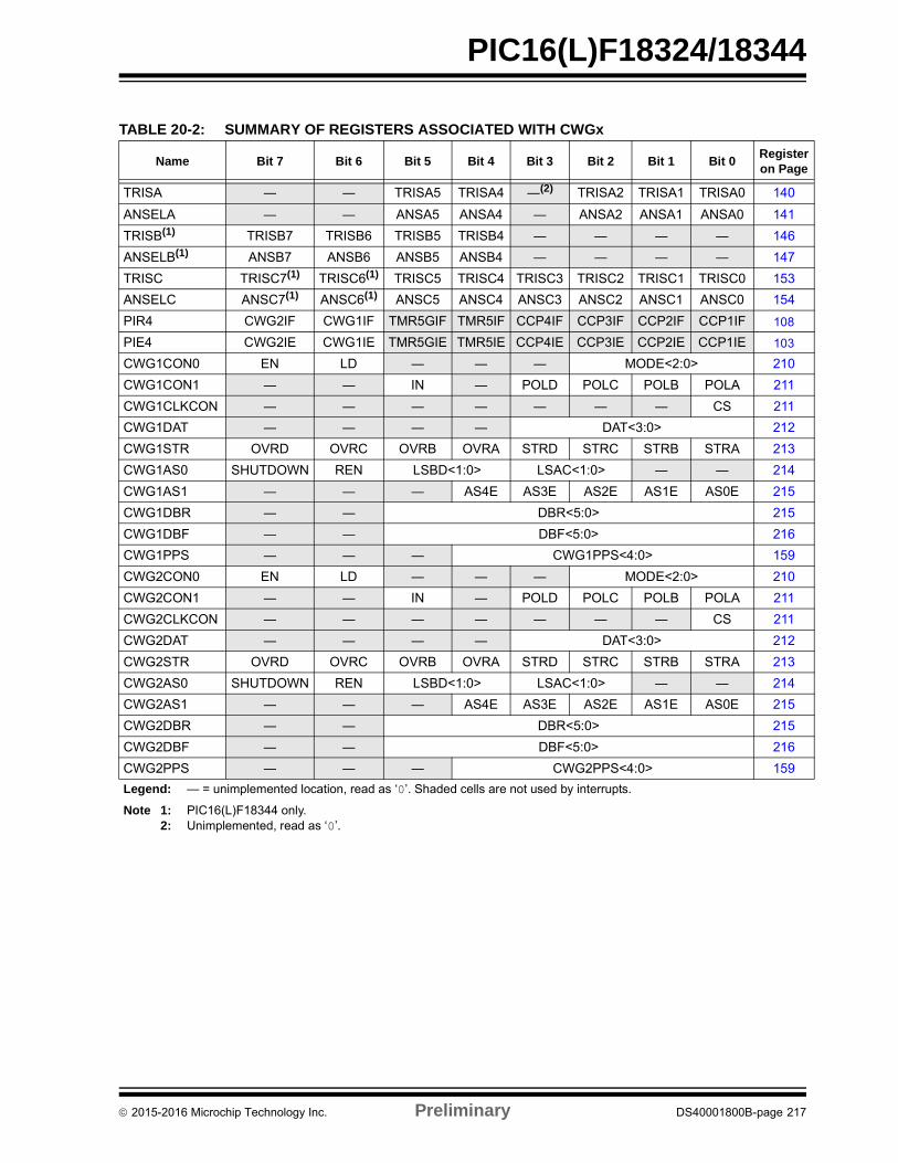
PIC16(L)F18324/18344
TABLE 20-2: SUMMARY OF REGISTERS ASSOCIATED WITH CWGx
Name Bit 7 Bit 6 Bit 5 Bit 4 Bit 3 Bit 2 Bit 1 Bit 0Register on Page
TRISA ― ― TRISA5 TRISA4 ―(2) TRISA2 TRISA1 TRISA0 140
ANSELA ― ― ANSA5 ANSA4 ― ANSA2 ANSA1 ANSA0 141
TRISB(1) TRISB7 TRISB6 TRISB5 TRISB4 ― ― ― ― 146
ANSELB(1) ANSB7 ANSB6 ANSB5 ANSB4 ― ― ― ― 147
TRISC TRISC7(1) TRISC6(1) TRISC5 TRISC4 TRISC3 TRISC2 TRISC1 TRISC0 153
ANSELC ANSC7(1) ANSC6(1) ANSC5 ANSC4 ANSC3 ANSC2 ANSC1 ANSC0 154
PIR4 CWG2IF CWG1IF TMR5GIF TMR5IF CCP4IF CCP3IF CCP2IF CCP1IF 108
PIE4 CWG2IE CWG1IE TMR5GIE TMR5IE CCP4IE CCP3IE CCP2IE CCP1IE 103
CWG1CON0 EN LD ― ― ― MODE<2:0> 210
CWG1CON1 ― ― IN ― POLD POLC POLB POLA 211
CWG1CLKCON ― ― ― ― ― ― ― CS 211
CWG1DAT ― ― ― ― DAT<3:0> 212
CWG1STR OVRD OVRC OVRB OVRA STRD STRC STRB STRA 213
CWG1AS0 SHUTDOWN REN LSBD<1:0> LSAC<1:0> ― ― 214
CWG1AS1 ― ― ― AS4E AS3E AS2E AS1E AS0E 215
CWG1DBR ― ― DBR<5:0> 215
CWG1DBF ― ― DBF<5:0> 216
CWG1PPS ― ― ― CWG1PPS<4:0> 159
CWG2CON0 EN LD ― ― ― MODE<2:0> 210
CWG2CON1 ― ― IN ― POLD POLC POLB POLA 211
CWG2CLKCON ― ― ― ― ― ― ― CS 211
CWG2DAT ― ― ― ― DAT<3:0> 212
CWG2STR OVRD OVRC OVRB OVRA STRD STRC STRB STRA 213
CWG2AS0 SHUTDOWN REN LSBD<1:0> LSAC<1:0> ― ― 214
CWG2AS1 ― ― ― AS4E AS3E AS2E AS1E AS0E 215
CWG2DBR ― ― DBR<5:0> 215
CWG2DBF ― ― DBF<5:0> 216
CWG2PPS ― ― ― CWG2PPS<4:0> 159
Legend: — = unimplemented location, read as ‘0’. Shaded cells are not used by interrupts.
Note 1: PIC16(L)F18344 only.2: Unimplemented, read as ‘0’.
2015-2016 Microchip Technology Inc. Preliminary DS40001800B-page 217
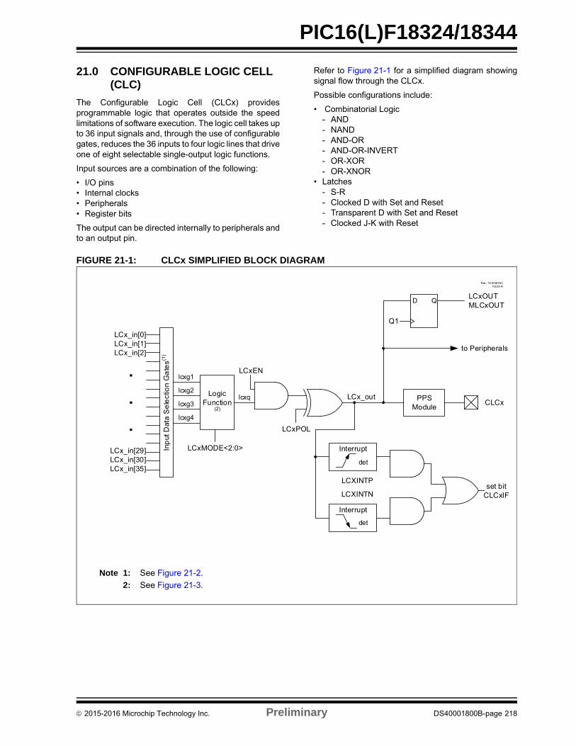
PIC16(L)F18324/18344
21.0 CONFIGURABLE LOGIC CELL (CLC)
The Configurable Logic Cell (CLCx) providesprogrammable logic that operates outside the speedlimitations of software execution. The logic cell takes upto 36 input signals and, through the use of configurablegates, reduces the 36 inputs to four logic lines that driveone of eight selectable single-output logic functions.
Input sources are a combination of the following:
• I/O pins• Internal clocks• Peripherals• Register bits
The output can be directed internally to peripherals andto an output pin.
Refer to Figure 21-1 for a simplified diagram showingsignal flow through the CLCx.
Possible configurations include:
• Combinatorial Logic- AND- NAND- AND-OR- AND-OR-INVERT- OR-XOR- OR-XNOR
• Latches- S-R- Clocked D with Set and Reset- Transparent D with Set and Reset- Clocked J-K with Reset
FIGURE 21-1: CLCx SIMPLIFIED BLOCK DIAGRAM
Inpu
t Dat
a S
elec
tion
Gat
es(1
)
LogicFunction
(2)
lcxg2
lcxg1
lcxg3
lcxg4
LCxMODE<2:0>
lcxq
LCxEN
LCxPOL
det
Interrupt
det
Interrupt
set bitCLCxIFLCXINTN
LCXINTP
CLCx
to Peripherals
Q1
LCx_out
LCxOUTMLCxOUTD Q
PPSModule
LCx_in[0]LCx_in[1]LCx_in[2]
LCx_in[29]LCx_in[30]LCx_in[35]
.
.
.
Rev. 10-000025C4/3/2014
Note 1: See Figure 21-2.
2: See Figure 21-3.
2015-2016 Microchip Technology Inc. Preliminary DS40001800B-page 218

PIC16(L)F18324/18344
21.1 CLCx Setup
Programming the CLCx module is performed by config-uring the four stages in the logic signal flow. The fourstages are:
• Data selection• Data gating• Logic function selection• Output polarity
Each stage is setup at run time by writing to the corre-sponding CLCx Special Function Registers. This hasthe added advantage of permitting logic reconfigurationon-the-fly during program execution.
21.1.1 DATA SELECTION
There are 36 signals available as inputs to theconfigurable logic.
Data selection is through four multiplexers as indicatedon the left side of Figure 21-2. Data inputs in the figureare identified by the ‘LCx_in’ signal name.
Table 21-1 correlates the input number to the actualsignal for each CLC module. The column labeled‘LCxDyS<5:0> Value’ indicates the MUX selection codefor the selected data input. LCxDyS is an abbreviation toidentify the specific input multiplexer: LCxD1S<5:0>through LCxD4S<5:0>.
Data inputs are selected with CLCxSEL0 throughCLCxSEL3 registers (Register 21-3 throughRegister 21-6).
TABLE 21-1: CLCx DATA INPUT SELECTION
LCxDyS<5:0>Value
CLCx Input Source
100011 [35] TMR6/PR6 match
100010 [34] TMR5 overflow
100001 [33] TMR4/PR4 match
100000 [32] TMR3 overflow
11111 [31] FOSC
11110 [30] HFINTOSC
11101 [29] LFINTOSC
11100 [28] ADCRC
11011 [27] IOCIF int flag bit
11010 [26] TMR2/PR2 match
11001 [25] TMR1 overflow
11000 [24] TMR0 overflow
10111 [23] EUSART (DT) output
10110 [22] EUSART (TX/CK) output
10101 [21] Reserved
10100 [20] Reserved
10011 [19] SDA1
10010 [18] SCL1
10001 [17] PWM6 output
10000 [16] PWM5 output
01111 [15] CCP4 output
01110 [14] CCP3 output
01101 [13] CCP2 output
01100 [12] CCP1 output
01011 [11] CLKR output
01010 [10] DSM output
01001 [9] C2 output
01000 [8] C1 output
00111 [7] CLC4 output
00110 [6] CLC3 output
00101 [5] CLC2 output
00100 [4] CLC1 output
00011 [3] CLCIN3PPS
00010 [2] CLCIN2PPS
00001 [1] CLCIN1PPS
00000 [0] CLCIN0PPS
2015-2016 Microchip Technology Inc. Preliminary DS40001800B-page 219
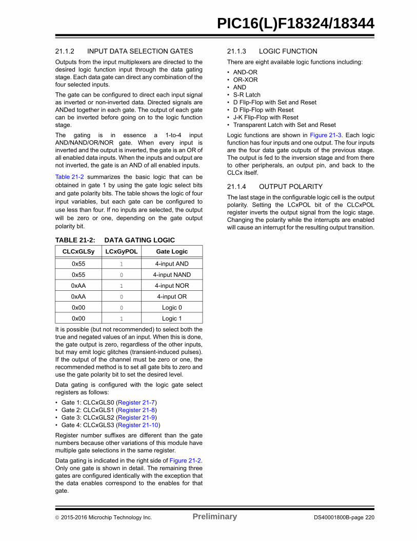
PIC16(L)F18324/18344
21.1.2 INPUT DATA SELECTION GATES
Outputs from the input multiplexers are directed to thedesired logic function input through the data gatingstage. Each data gate can direct any combination of thefour selected inputs.
The gate can be configured to direct each input signalas inverted or non-inverted data. Directed signals areANDed together in each gate. The output of each gatecan be inverted before going on to the logic functionstage.
The gating is in essence a 1-to-4 inputAND/NAND/OR/NOR gate. When every input isinverted and the output is inverted, the gate is an OR ofall enabled data inputs. When the inputs and output arenot inverted, the gate is an AND of all enabled inputs.
Table 21-2 summarizes the basic logic that can beobtained in gate 1 by using the gate logic select bitsand gate polarity bits. The table shows the logic of fourinput variables, but each gate can be configured touse less than four. If no inputs are selected, the outputwill be zero or one, depending on the gate outputpolarity bit.
It is possible (but not recommended) to select both thetrue and negated values of an input. When this is done,the gate output is zero, regardless of the other inputs,but may emit logic glitches (transient-induced pulses).If the output of the channel must be zero or one, therecommended method is to set all gate bits to zero anduse the gate polarity bit to set the desired level.
Data gating is configured with the logic gate selectregisters as follows:
• Gate 1: CLCxGLS0 (Register 21-7)• Gate 2: CLCxGLS1 (Register 21-8)• Gate 3: CLCxGLS2 (Register 21-9)• Gate 4: CLCxGLS3 (Register 21-10)
Register number suffixes are different than the gatenumbers because other variations of this module havemultiple gate selections in the same register.
Data gating is indicated in the right side of Figure 21-2.Only one gate is shown in detail. The remaining threegates are configured identically with the exception thatthe data enables correspond to the enables for thatgate.
21.1.3 LOGIC FUNCTION
There are eight available logic functions including:
• AND-OR• OR-XOR• AND• S-R Latch• D Flip-Flop with Set and Reset• D Flip-Flop with Reset• J-K Flip-Flop with Reset• Transparent Latch with Set and Reset
Logic functions are shown in Figure 21-3. Each logicfunction has four inputs and one output. The four inputsare the four data gate outputs of the previous stage.The output is fed to the inversion stage and from thereto other peripherals, an output pin, and back to theCLCx itself.
21.1.4 OUTPUT POLARITY
The last stage in the configurable logic cell is the outputpolarity. Setting the LCxPOL bit of the CLCxPOLregister inverts the output signal from the logic stage.Changing the polarity while the interrupts are enabledwill cause an interrupt for the resulting output transition.
TABLE 21-2: DATA GATING LOGIC
CLCxGLSy LCxGyPOL Gate Logic
0x55 1 4-input AND
0x55 0 4-input NAND
0xAA 1 4-input NOR
0xAA 0 4-input OR
0x00 0 Logic 0
0x00 1 Logic 1
2015-2016 Microchip Technology Inc. Preliminary DS40001800B-page 220
PIC16(L)F18324/18344
21.2 CLCx Interrupts
An interrupt will be generated upon a change in theoutput value of the CLCx when the appropriate interruptenables are set. A rising edge detector and a fallingedge detector are present in each CLC for this purpose.
The CLCxIF bit of the associated PIR3 register will beset when either edge detector is triggered and itsassociated enable bit is set. The LCxINTP bit enablesrising edge interrupts and the LCxINTN bit enablesfalling edge interrupts. Both are located in theCLCxCON register.
To fully enable the interrupt, set the following bits:
• CLCxIE bit of the PIE3 register• LCxINTP bit of the CLCxCON register (for a rising
edge detection)• LCxINTN bit of the CLCxCON register (for a
falling edge detection)• PEIE and GIE bits of the INTCON register
The CLCxIF bit of the PIR3 register, must be cleared insoftware as part of the interrupt service. If another edgeis detected while this flag is being cleared, the flag willstill be set at the end of the sequence.
21.3 Output Mirror Copies
Mirror copies of all LCxCON output bits are containedin the CLCDATA register. Reading this registersamples the outputs of all CLCs simultaneously. Thisprevents any timing skew introduced by testing orreading the LCxOUT bits in the individual CLCxCONregisters.
21.4 Effects of a Reset
The CLCxCON register is cleared to zero as the resultof a Reset. All other selection and gating values remainunchanged.
21.5 Operation During Sleep
The CLC module operates independently from thesystem clock and will continue to run during Sleep,provided that the input sources selected remain active.
The HFINTOSC remains active during Sleep when theCLC module is enabled and the HFINTOSC isselected as an input source, regardless of the systemclock source selected.
In other words, if the HFINTOSC is simultaneouslyselected as the system clock and as a CLC inputsource, when the CLC is enabled, the CPU will go idleduring Sleep, but the CLC will continue to operate andthe HFINTOSC will remain active.
This will have a direct effect on the Sleep mode current.
21.6 CLCx Setup Steps
The following steps should be followed when setting upthe CLCx:
• Disable CLCx by clearing the LCxEN bit.• Select desired inputs using CLCxSEL0 through
CLCxSEL3 registers (See Table 21-1).• Clear any associated ANSEL bits.• Set all TRIS bits associated with external inputs.• Enable the chosen inputs through the four gates
using CLCxGLS0, CLCxGLS1, CLCxGLS2, and CLCxGLS3 registers.
• Select the gate output polarities with the LCxGyPOL bits of the CLCxPOL register.
• Select the desired logic function with the LCx-MODE<2:0> bits of the CLCxCON register.
• Select the desired polarity of the logic output with the LCxPOL bit of the CLCxPOL register. (This step may be combined with the previous gate out-put polarity step).
• If driving a device pin, set the desired pin PPS control register and also clear the TRIS bit corresponding to that output.
• If interrupts are desired, configure the following bits:- Set the LCxINTP bit in the CLCxCON register
for rising event.- Set the LCxINTN bit in the CLCxCON regis-
ter for falling event.- Set the CLCxIE bit of the PIE3 register.- Set the GIE and PEIE bits of the INTCON
register.• Enable the CLCx by setting the LCxEN bit of the
CLCxCON register.
2015-2016 Microchip Technology Inc. Preliminary DS40001800B-page 221
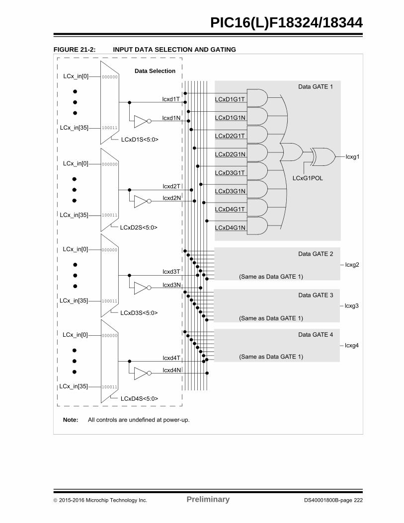
PIC16(L)F18324/18344
FIGURE 21-2: INPUT DATA SELECTION AND GATING
lcxg1
LCxG1POL
Data GATE 1
LCxD1G1T
lcxg2
lcxg3
lcxg4
Data GATE 2
Data GATE 3
Data GATE 4
LCxD1G1N
LCxD2G1T
LCxD2G1N
LCxD3G1T
LCxD3G1N
LCxD4G1T
LCxD4G1N
LCxD1S<5:0>
LCxD2S<5:0>
LCxD3S<5:0>
LCxD4S<5:0>
LCx_in[0]
LCx_in[35]
000000
100011
Data Selection
Note: All controls are undefined at power-up.
lcxd1T
lcxd1N
lcxd2T
lcxd2N
lcxd3T
lcxd3N
lcxd4T
lcxd4N
(Same as Data GATE 1)
(Same as Data GATE 1)
(Same as Data GATE 1)
LCx_in[0]
LCx_in[35]
000000
100011
LCx_in[0]
LCx_in[35]
000000
100011
LCx_in[0]
LCx_in[35]
000000
100011
Data GATE 3
(Same as Data GATE 1)
2015-2016 Microchip Technology Inc. Preliminary DS40001800B-page 222
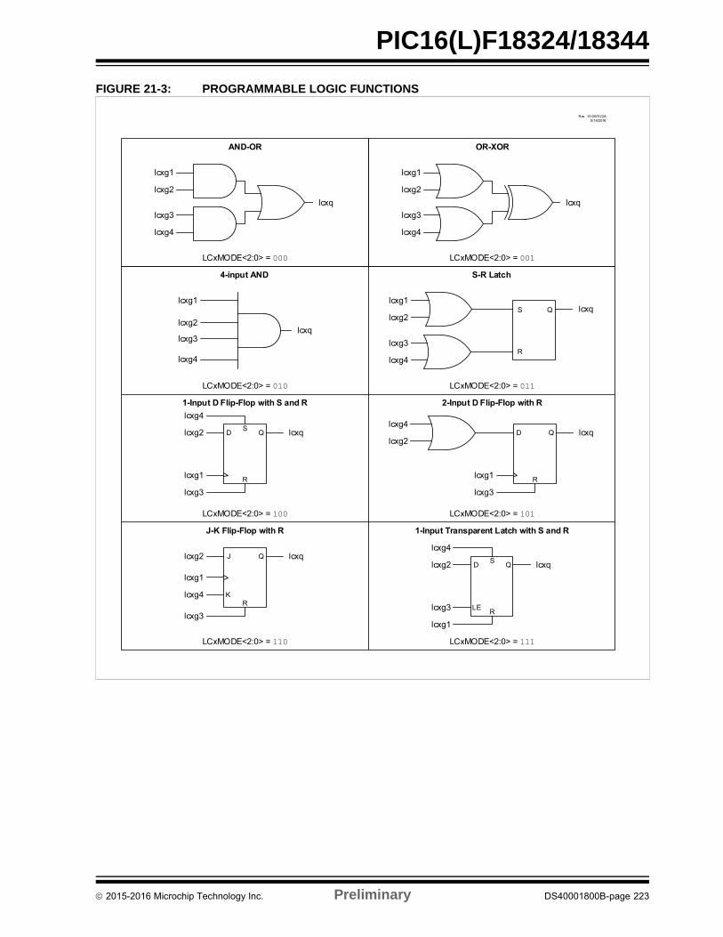
PIC16(L)F18324/18344
FIGURE 21-3: PROGRAMMABLE LOGIC FUNCTIONS
lcxg1
lcxg2
lcxg3
lcxg4
lcxq
AND-OR OR-XOR
LCxMODE<2:0> = 000 LCxMODE<2:0> = 0014-input AND S-R Latch
LCxMODE<2:0> = 010 LCxMODE<2:0> = 011
lcxg1
lcxg2
lcxg3
lcxg4
lcxq
S
R
Q lcxqlcxg1
lcxg2
lcxg3
lcxg4
lcxg1
lcxg2
lcxg3
lcxg4
lcxq
1-Input D Flip-Flop with S and R 2-Input D Flip-Flop with R
J-K Flip-Flop with R 1-Input Transparent Latch with S and R
LCxMODE<2:0> = 100 LCxMODE<2:0> = 101
LCxMODE<2:0> = 110 LCxMODE<2:0> = 111
D
R
Q lcxq
lcxg1
lcxg2
lcxg3
lcxg4D
R
QS
lcxg1
lcxg2
lcxg3
lcxg4
lcxq
J
R
Q
K
lcxg1
lcxg2
lcxg3
lcxg4
lcxqD
R
QS
LE
lcxq
lcxg1
lcxg2
lcxg3
lcxg4
Rev. 10-000122A5/18/2016
2015-2016 Microchip Technology Inc. Preliminary DS40001800B-page 223
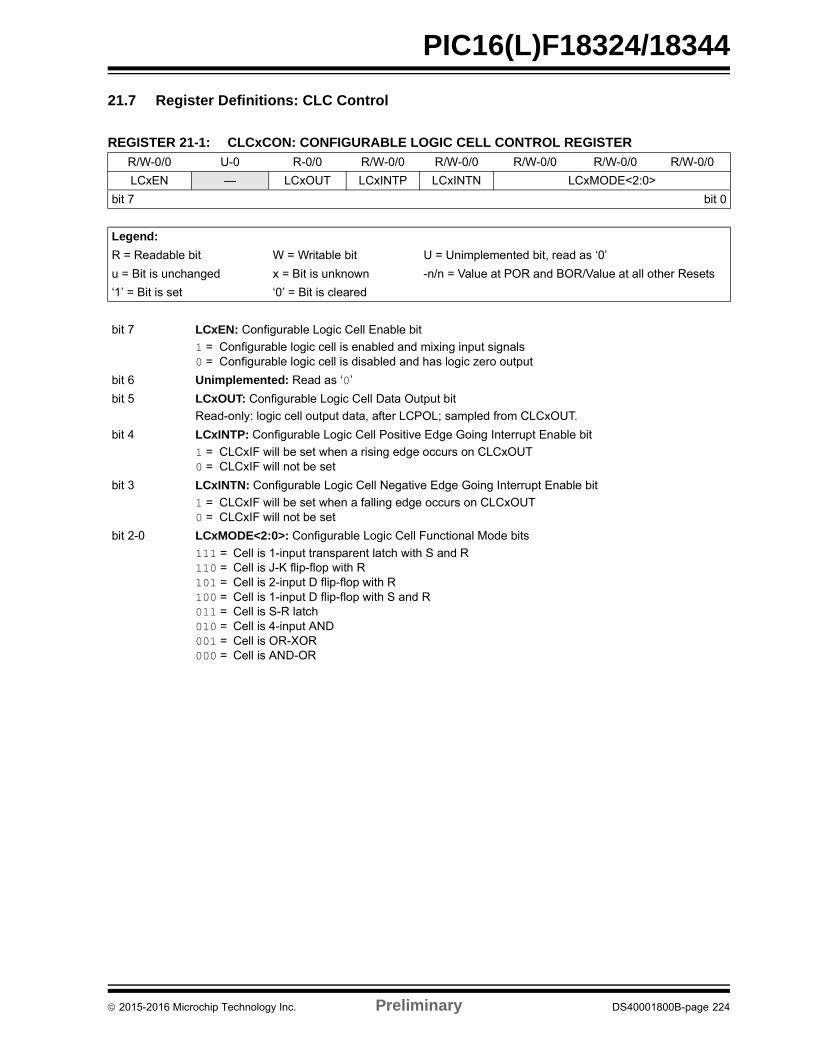
PIC16(L)F18324/18344
21.7 Register Definitions: CLC Control
REGISTER 21-1: CLCxCON: CONFIGURABLE LOGIC CELL CONTROL REGISTER
R/W-0/0 U-0 R-0/0 R/W-0/0 R/W-0/0 R/W-0/0 R/W-0/0 R/W-0/0
LCxEN — LCxOUT LCxINTP LCxINTN LCxMODE<2:0>
bit 7 bit 0
Legend:
R = Readable bit W = Writable bit U = Unimplemented bit, read as ‘0’
u = Bit is unchanged x = Bit is unknown -n/n = Value at POR and BOR/Value at all other Resets
‘1’ = Bit is set ‘0’ = Bit is cleared
bit 7 LCxEN: Configurable Logic Cell Enable bit
1 = Configurable logic cell is enabled and mixing input signals0 = Configurable logic cell is disabled and has logic zero output
bit 6 Unimplemented: Read as ‘0’
bit 5 LCxOUT: Configurable Logic Cell Data Output bit
Read-only: logic cell output data, after LCPOL; sampled from CLCxOUT.
bit 4 LCxINTP: Configurable Logic Cell Positive Edge Going Interrupt Enable bit
1 = CLCxIF will be set when a rising edge occurs on CLCxOUT0 = CLCxIF will not be set
bit 3 LCxINTN: Configurable Logic Cell Negative Edge Going Interrupt Enable bit
1 = CLCxIF will be set when a falling edge occurs on CLCxOUT0 = CLCxIF will not be set
bit 2-0 LCxMODE<2:0>: Configurable Logic Cell Functional Mode bits
111 = Cell is 1-input transparent latch with S and R110 = Cell is J-K flip-flop with R101 = Cell is 2-input D flip-flop with R100 = Cell is 1-input D flip-flop with S and R011 = Cell is S-R latch010 = Cell is 4-input AND001 = Cell is OR-XOR000 = Cell is AND-OR
2015-2016 Microchip Technology Inc. Preliminary DS40001800B-page 224
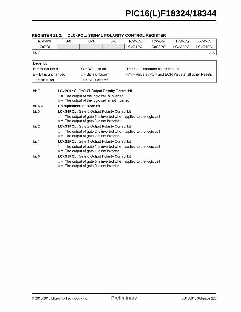
PIC16(L)F18324/18344
REGISTER 21-2: CLCxPOL: SIGNAL POLARITY CONTROL REGISTER
R/W-0/0 U-0 U-0 U-0 R/W-x/u R/W-x/u R/W-x/u R/W-x/u
LCxPOL — — — LCxG4POL LCxG3POL LCxG2POL LCxG1POL
bit 7 bit 0
Legend:
R = Readable bit W = Writable bit U = Unimplemented bit, read as ‘0’
u = Bit is unchanged x = Bit is unknown -n/n = Value at POR and BOR/Value at all other Resets
‘1’ = Bit is set ‘0’ = Bit is cleared
bit 7 LCxPOL: CLCxOUT Output Polarity Control bit
1 = The output of the logic cell is inverted0 = The output of the logic cell is not inverted
bit 6-4 Unimplemented: Read as ‘0’
bit 3 LCxG4POL: Gate 3 Output Polarity Control bit
1 = The output of gate 3 is inverted when applied to the logic cell0 = The output of gate 3 is not inverted
bit 2 LCxG3POL: Gate 2 Output Polarity Control bit
1 = The output of gate 2 is inverted when applied to the logic cell0 = The output of gate 2 is not inverted
bit 1 LCxG2POL: Gate 1 Output Polarity Control bit
1 = The output of gate 1 is inverted when applied to the logic cell0 = The output of gate 1 is not inverted
bit 0 LCxG1POL: Gate 0 Output Polarity Control bit
1 = The output of gate 0 is inverted when applied to the logic cell0 = The output of gate 0 is not inverted
2015-2016 Microchip Technology Inc. Preliminary DS40001800B-page 225
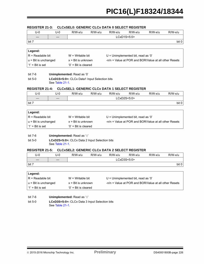
PIC16(L)F18324/18344
REGISTER 21-3: CLCxSEL0: GENERIC CLCx DATA 0 SELECT REGISTER
U-0 U-0 R/W-x/u R/W-x/u R/W-x/u R/W-x/u R/W-x/u R/W-x/u
— — LCxD1S<5:0>
bit 7 bit 0
Legend:
R = Readable bit W = Writable bit U = Unimplemented bit, read as ‘0’
u = Bit is unchanged x = Bit is unknown -n/n = Value at POR and BOR/Value at all other Resets
‘1’ = Bit is set ‘0’ = Bit is cleared
bit 7-6 Unimplemented: Read as ‘0’
bit 5-0 LCxD1S<5:0>: CLCx Data1 Input Selection bitsSee Table 21-1.
REGISTER 21-4: CLCxSEL1: GENERIC CLCx DATA 1 SELECT REGISTER
U-0 U-0 R/W-x/u R/W-x/u R/W-x/u R/W-x/u R/W-x/u R/W-x/u
— — LCxD2S<5:0>
bit 7 bit 0
Legend:
R = Readable bit W = Writable bit U = Unimplemented bit, read as ‘0’
u = Bit is unchanged x = Bit is unknown -n/n = Value at POR and BOR/Value at all other Resets
‘1’ = Bit is set ‘0’ = Bit is cleared
bit 7-6 Unimplemented: Read as ‘0’
bit 5-0 LCxD2S<5:0>: CLCx Data 2 Input Selection bitsSee Table 21-1.
REGISTER 21-5: CLCxSEL2: GENERIC CLCx DATA 2 SELECT REGISTER
U-0 U-0 R/W-x/u R/W-x/u R/W-x/u R/W-x/u R/W-x/u R/W-x/u
— — LCxD3S<5:0>
bit 7 bit 0
Legend:
R = Readable bit W = Writable bit U = Unimplemented bit, read as ‘0’
u = Bit is unchanged x = Bit is unknown -n/n = Value at POR and BOR/Value at all other Resets
‘1’ = Bit is set ‘0’ = Bit is cleared
bit 7-6 Unimplemented: Read as ‘0’
bit 5-0 LCxD3S<5:0>: CLCx Data 3 Input Selection bitsSee Table 21-1.
2015-2016 Microchip Technology Inc. Preliminary DS40001800B-page 226
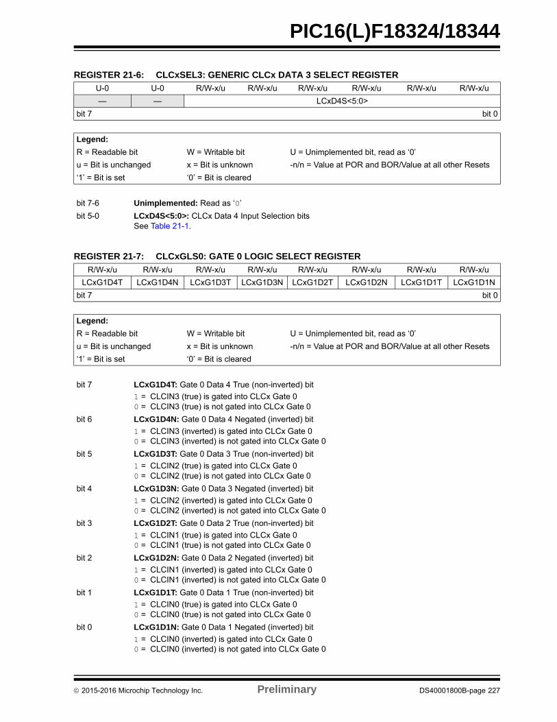
PIC16(L)F18324/18344
REGISTER 21-6: CLCxSEL3: GENERIC CLCx DATA 3 SELECT REGISTER
U-0 U-0 R/W-x/u R/W-x/u R/W-x/u R/W-x/u R/W-x/u R/W-x/u
— — LCxD4S<5:0>
bit 7 bit 0
Legend:
R = Readable bit W = Writable bit U = Unimplemented bit, read as ‘0’
u = Bit is unchanged x = Bit is unknown -n/n = Value at POR and BOR/Value at all other Resets
‘1’ = Bit is set ‘0’ = Bit is cleared
bit 7-6 Unimplemented: Read as ‘0’
bit 5-0 LCxD4S<5:0>: CLCx Data 4 Input Selection bitsSee Table 21-1.
REGISTER 21-7: CLCxGLS0: GATE 0 LOGIC SELECT REGISTER
R/W-x/u R/W-x/u R/W-x/u R/W-x/u R/W-x/u R/W-x/u R/W-x/u R/W-x/u
LCxG1D4T LCxG1D4N LCxG1D3T LCxG1D3N LCxG1D2T LCxG1D2N LCxG1D1T LCxG1D1N
bit 7 bit 0
Legend:
R = Readable bit W = Writable bit U = Unimplemented bit, read as ‘0’
u = Bit is unchanged x = Bit is unknown -n/n = Value at POR and BOR/Value at all other Resets
‘1’ = Bit is set ‘0’ = Bit is cleared
bit 7 LCxG1D4T: Gate 0 Data 4 True (non-inverted) bit
1 = CLCIN3 (true) is gated into CLCx Gate 00 = CLCIN3 (true) is not gated into CLCx Gate 0
bit 6 LCxG1D4N: Gate 0 Data 4 Negated (inverted) bit
1 = CLCIN3 (inverted) is gated into CLCx Gate 00 = CLCIN3 (inverted) is not gated into CLCx Gate 0
bit 5 LCxG1D3T: Gate 0 Data 3 True (non-inverted) bit
1 = CLCIN2 (true) is gated into CLCx Gate 00 = CLCIN2 (true) is not gated into CLCx Gate 0
bit 4 LCxG1D3N: Gate 0 Data 3 Negated (inverted) bit
1 = CLCIN2 (inverted) is gated into CLCx Gate 00 = CLCIN2 (inverted) is not gated into CLCx Gate 0
bit 3 LCxG1D2T: Gate 0 Data 2 True (non-inverted) bit
1 = CLCIN1 (true) is gated into CLCx Gate 00 = CLCIN1 (true) is not gated into CLCx Gate 0
bit 2 LCxG1D2N: Gate 0 Data 2 Negated (inverted) bit
1 = CLCIN1 (inverted) is gated into CLCx Gate 00 = CLCIN1 (inverted) is not gated into CLCx Gate 0
bit 1 LCxG1D1T: Gate 0 Data 1 True (non-inverted) bit
1 = CLCIN0 (true) is gated into CLCx Gate 00 = CLCIN0 (true) is not gated into CLCx Gate 0
bit 0 LCxG1D1N: Gate 0 Data 1 Negated (inverted) bit
1 = CLCIN0 (inverted) is gated into CLCx Gate 00 = CLCIN0 (inverted) is not gated into CLCx Gate 0
2015-2016 Microchip Technology Inc. Preliminary DS40001800B-page 227

PIC16(L)F18324/18344
REGISTER 21-8: CLCxGLS1: GATE 1 LOGIC SELECT REGISTER
R/W-x/u R/W-x/u R/W-x/u R/W-x/u R/W-x/u R/W-x/u R/W-x/u R/W-x/u
LCxG2D4T LCxG2D4N LCxG2D3T LCxG2D3N LCxG2D2T LCxG2D2N LCxG2D1T LCxG2D1N
bit 7 bit 0
Legend:
R = Readable bit W = Writable bit U = Unimplemented bit, read as ‘0’
u = Bit is unchanged x = Bit is unknown -n/n = Value at POR and BOR/Value at all other Resets
‘1’ = Bit is set ‘0’ = Bit is cleared
bit 7 LCxG2D4T: Gate 1 Data 4 True (non-inverted) bit
1 = CLCIN3 (true) is gated into CLCx Gate 10 = CLCIN3 (true) is not gated into CLCx Gate 1
bit 6 LCxG2D4N: Gate 1 Data 4 Negated (inverted) bit
1 = CLCIN3 (inverted) is gated into CLCx Gate 10 = CLCIN3 (inverted) is not gated into CLCx Gate 1
bit 5 LCxG2D3T: Gate 1 Data 3 True (non-inverted) bit
1 = CLCIN2 (true) is gated into CLCx Gate 10 = CLCIN2 (true) is not gated into CLCx Gate 1
bit 4 LCxG2D3N: Gate 1 Data 3 Negated (inverted) bit
1 = CLCIN2 (inverted) is gated into CLCx Gate 10 = CLCIN2 (inverted) is not gated into CLCx Gate 1
bit 3 LCxG2D2T: Gate 1 Data 2 True (non-inverted) bit
1 = CLCIN1 (true) is gated into CLCx Gate 10 = CLCIN1 (true) is not gated into CLCx Gate 1
bit 2 LCxG2D2N: Gate 1 Data 2 Negated (inverted) bit
1 = CLCIN1 (inverted) is gated into CLCx Gate 10 = CLCIN1 (inverted) is not gated into CLCx Gate 1
bit 1 LCxG2D1T: Gate 1 Data 1 True (non-inverted) bit
1 = CLCIN0 (true) is gated into CLCx Gate 10 = CLCIN0 (true) is not gated into CLCx Gate 1
bit 0 LCxG2D1N: Gate 1 Data 1 Negated (inverted) bit
1 = CLCIN0 (inverted) is gated into CLCx Gate 10 = CLCIN0 (inverted) is not gated into CLCx Gate 1
2015-2016 Microchip Technology Inc. Preliminary DS40001800B-page 228
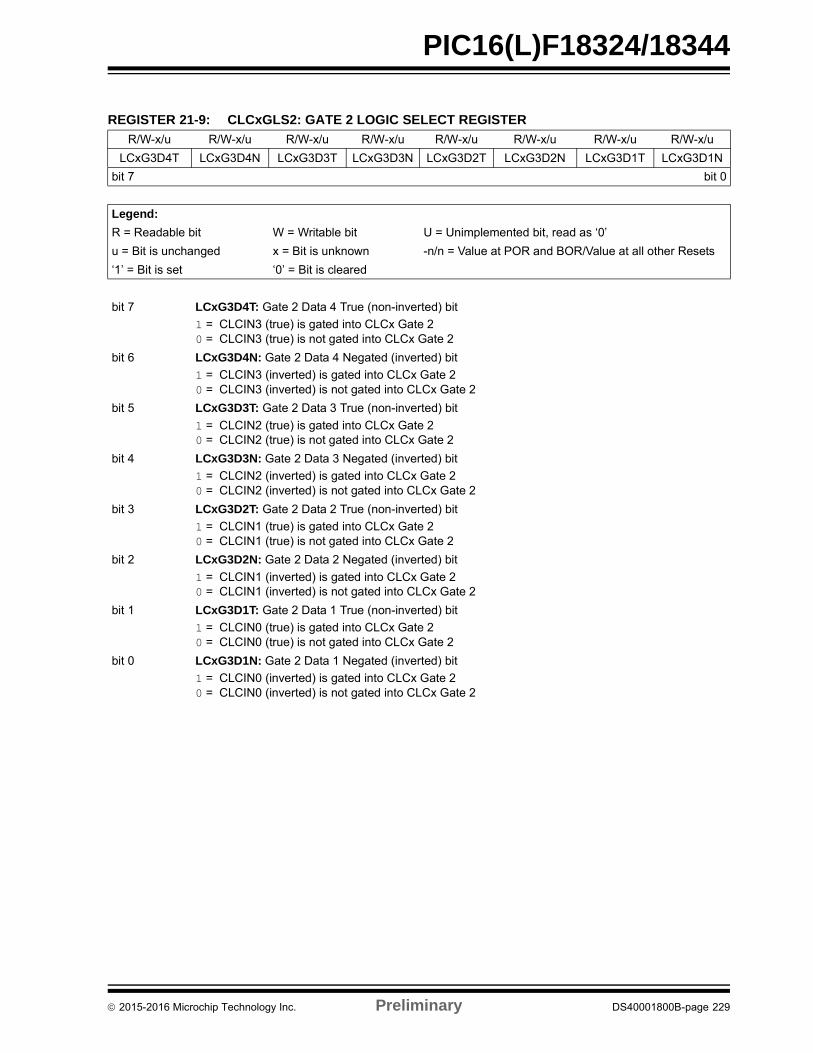
PIC16(L)F18324/18344
REGISTER 21-9: CLCxGLS2: GATE 2 LOGIC SELECT REGISTER
R/W-x/u R/W-x/u R/W-x/u R/W-x/u R/W-x/u R/W-x/u R/W-x/u R/W-x/u
LCxG3D4T LCxG3D4N LCxG3D3T LCxG3D3N LCxG3D2T LCxG3D2N LCxG3D1T LCxG3D1N
bit 7 bit 0
Legend:
R = Readable bit W = Writable bit U = Unimplemented bit, read as ‘0’
u = Bit is unchanged x = Bit is unknown -n/n = Value at POR and BOR/Value at all other Resets
‘1’ = Bit is set ‘0’ = Bit is cleared
bit 7 LCxG3D4T: Gate 2 Data 4 True (non-inverted) bit
1 = CLCIN3 (true) is gated into CLCx Gate 20 = CLCIN3 (true) is not gated into CLCx Gate 2
bit 6 LCxG3D4N: Gate 2 Data 4 Negated (inverted) bit
1 = CLCIN3 (inverted) is gated into CLCx Gate 20 = CLCIN3 (inverted) is not gated into CLCx Gate 2
bit 5 LCxG3D3T: Gate 2 Data 3 True (non-inverted) bit
1 = CLCIN2 (true) is gated into CLCx Gate 20 = CLCIN2 (true) is not gated into CLCx Gate 2
bit 4 LCxG3D3N: Gate 2 Data 3 Negated (inverted) bit
1 = CLCIN2 (inverted) is gated into CLCx Gate 20 = CLCIN2 (inverted) is not gated into CLCx Gate 2
bit 3 LCxG3D2T: Gate 2 Data 2 True (non-inverted) bit
1 = CLCIN1 (true) is gated into CLCx Gate 20 = CLCIN1 (true) is not gated into CLCx Gate 2
bit 2 LCxG3D2N: Gate 2 Data 2 Negated (inverted) bit
1 = CLCIN1 (inverted) is gated into CLCx Gate 20 = CLCIN1 (inverted) is not gated into CLCx Gate 2
bit 1 LCxG3D1T: Gate 2 Data 1 True (non-inverted) bit
1 = CLCIN0 (true) is gated into CLCx Gate 20 = CLCIN0 (true) is not gated into CLCx Gate 2
bit 0 LCxG3D1N: Gate 2 Data 1 Negated (inverted) bit
1 = CLCIN0 (inverted) is gated into CLCx Gate 20 = CLCIN0 (inverted) is not gated into CLCx Gate 2
2015-2016 Microchip Technology Inc. Preliminary DS40001800B-page 229

PIC16(L)F18324/18344
REGISTER 21-10: CLCxGLS3: GATE 3 LOGIC SELECT REGISTER
R/W-x/u R/W-x/u R/W-x/u R/W-x/u R/W-x/u R/W-x/u R/W-x/u R/W-x/u
LCxG4D4T LCxG4D4N LCxG4D3T LCxG4D3N LCxG4D2T LCxG4D2N LCxG4D1T LCxG4D1N
bit 7 bit 0
Legend:
R = Readable bit W = Writable bit U = Unimplemented bit, read as ‘0’
u = Bit is unchanged x = Bit is unknown -n/n = Value at POR and BOR/Value at all other Resets
‘1’ = Bit is set ‘0’ = Bit is cleared
bit 7 LCxG4D4T: Gate 3 Data 4 True (non-inverted) bit
1 = CLCIN3 (true) is gated into CLCx Gate 30 = CLCIN3 (true) is not gated into CLCx Gate 3
bit 6 LCxG4D4N: Gate 3 Data 4 Negated (inverted) bit
1 = CLCIN3 (inverted) is gated into CLCx Gate 30 = CLCIN3 (inverted) is not gated into CLCx Gate 3
bit 5 LCxG4D3T: Gate 3 Data 3 True (non-inverted) bit
1 = CLCIN2 (true) is gated into CLCx Gate 30 = CLCIN2 (true) is not gated into CLCx Gate 3
bit 4 LCxG4D3N: Gate 3 Data 3 Negated (inverted) bit
1 = CLCIN2 (inverted) is gated into CLCx Gate 30 = CLCIN2 (inverted) is not gated into CLCx Gate 3
bit 3 LCxG4D2T: Gate 3 Data 2 True (non-inverted) bit
1 = CLCIN1 (true) is gated into CLCx Gate 30 = CLCIN1 (true) is not gated into CLCx Gate 3
bit 2 LCxG4D2N: Gate 3 Data 2 Negated (inverted) bit
1 = CLCIN1 (inverted) is gated into CLCx Gate 30 = CLCIN1 (inverted) is not gated into CLCx Gate 3
bit 1 LCxG4D1T: Gate 3 Data 1 True (non-inverted) bit
1 = CLCIN0 (true) is gated into CLCx Gate 30 = CLCIN0 (true) is not gated into CLCx Gate 3
bit 0 LCxG4D1N: Gate 3 Data 1 Negated (inverted) bit
1 = CLCIN0 (inverted) is gated into CLCx Gate 30 = CLCIN0 (inverted) is not gated into CLCx Gate 3
2015-2016 Microchip Technology Inc. Preliminary DS40001800B-page 230
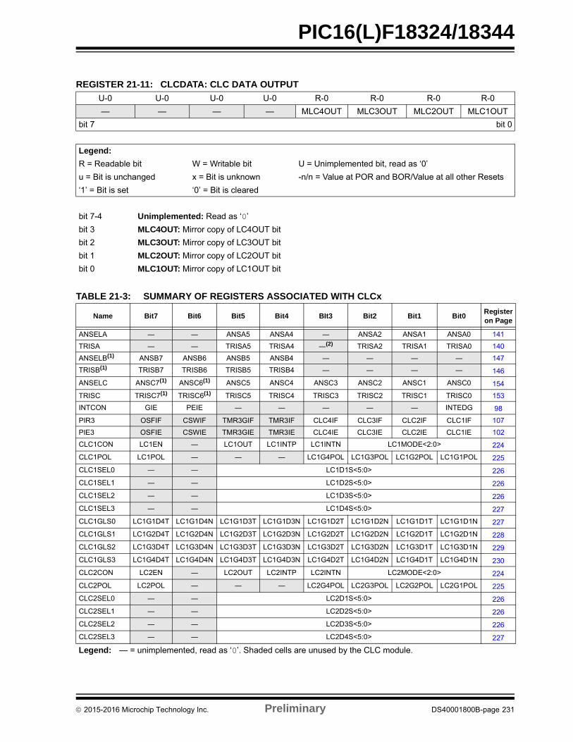
PIC16(L)F18324/18344
REGISTER 21-11: CLCDATA: CLC DATA OUTPUT
U-0 U-0 U-0 U-0 R-0 R-0 R-0 R-0
— — — — MLC4OUT MLC3OUT MLC2OUT MLC1OUT
bit 7 bit 0
Legend:
R = Readable bit W = Writable bit U = Unimplemented bit, read as ‘0’
u = Bit is unchanged x = Bit is unknown -n/n = Value at POR and BOR/Value at all other Resets
‘1’ = Bit is set ‘0’ = Bit is cleared
bit 7-4 Unimplemented: Read as ‘0’
bit 3 MLC4OUT: Mirror copy of LC4OUT bit
bit 2 MLC3OUT: Mirror copy of LC3OUT bit
bit 1 MLC2OUT: Mirror copy of LC2OUT bit
bit 0 MLC1OUT: Mirror copy of LC1OUT bit
TABLE 21-3: SUMMARY OF REGISTERS ASSOCIATED WITH CLCx
Name Bit7 Bit6 Bit5 Bit4 BIt3 Bit2 Bit1 Bit0Register on Page
ANSELA ― ― ANSA5 ANSA4 ― ANSA2 ANSA1 ANSA0 141
TRISA ― ― TRISA5 TRISA4 ―(2) TRISA2 TRISA1 TRISA0 140
ANSELB(1) ANSB7 ANSB6 ANSB5 ANSB4 ― ― ― ― 147
TRISB(1) TRISB7 TRISB6 TRISB5 TRISB4 ― ― ― ― 146
ANSELC ANSC7(1) ANSC6(1) ANSC5 ANSC4 ANSC3 ANSC2 ANSC1 ANSC0 154
TRISC TRISC7(1) TRISC6(1) TRISC5 TRISC4 TRISC3 TRISC2 TRISC1 TRISC0 153
INTCON GIE PEIE ― ― ― ― ― INTEDG 98
PIR3 OSFIF CSWIF TMR3GIF TMR3IF CLC4IF CLC3IF CLC2IF CLC1IF 107
PIE3 OSFIE CSWIE TMR3GIE TMR3IE CLC4IE CLC3IE CLC2IE CLC1IE 102
CLC1CON LC1EN ― LC1OUT LC1INTP LC1INTN LC1MODE<2:0> 224
CLC1POL LC1POL ― ― ― LC1G4POL LC1G3POL LC1G2POL LC1G1POL 225
CLC1SEL0 ― ― LC1D1S<5:0> 226
CLC1SEL1 ― ― LC1D2S<5:0> 226
CLC1SEL2 ― ― LC1D3S<5:0> 226
CLC1SEL3 ― ― LC1D4S<5:0> 227
CLC1GLS0 LC1G1D4T LC1G1D4N LC1G1D3T LC1G1D3N LC1G1D2T LC1G1D2N LC1G1D1T LC1G1D1N 227
CLC1GLS1 LC1G2D4T LC1G2D4N LC1G2D3T LC1G2D3N LC1G2D2T LC1G2D2N LC1G2D1T LC1G2D1N 228
CLC1GLS2 LC1G3D4T LC1G3D4N LC1G3D3T LC1G3D3N LC1G3D2T LC1G3D2N LC1G3D1T LC1G3D1N 229
CLC1GLS3 LC1G4D4T LC1G4D4N LC1G4D3T LC1G4D3N LC1G4D2T LC1G4D2N LC1G4D1T LC1G4D1N 230
CLC2CON LC2EN ― LC2OUT LC2INTP LC2INTN LC2MODE<2:0> 224
CLC2POL LC2POL ― ― ― LC2G4POL LC2G3POL LC2G2POL LC2G1POL 225
CLC2SEL0 ― ― LC2D1S<5:0> 226
CLC2SEL1 ― ― LC2D2S<5:0> 226
CLC2SEL2 ― ― LC2D3S<5:0> 226
CLC2SEL3 ― ― LC2D4S<5:0> 227
Legend: — = unimplemented, read as ‘0’. Shaded cells are unused by the CLC module.
2015-2016 Microchip Technology Inc. Preliminary DS40001800B-page 231
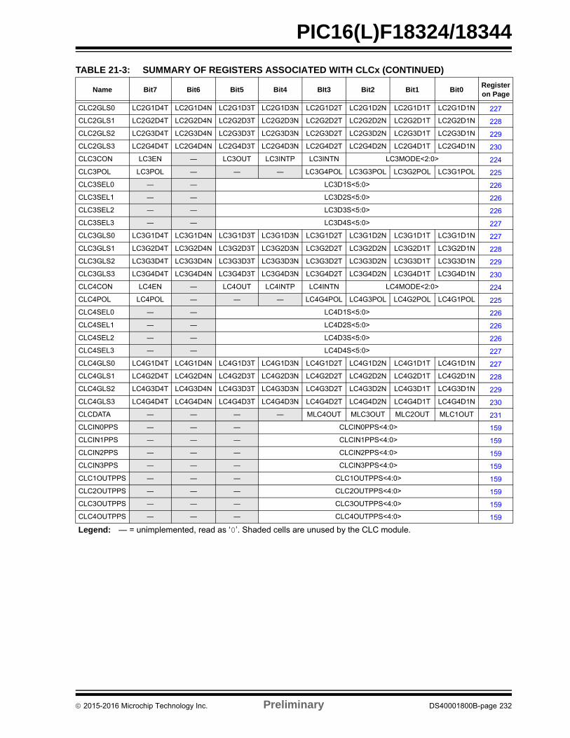
PIC16(L)F18324/18344
CLC2GLS0 LC2G1D4T LC2G1D4N LC2G1D3T LC2G1D3N LC2G1D2T LC2G1D2N LC2G1D1T LC2G1D1N 227
CLC2GLS1 LC2G2D4T LC2G2D4N LC2G2D3T LC2G2D3N LC2G2D2T LC2G2D2N LC2G2D1T LC2G2D1N 228
CLC2GLS2 LC2G3D4T LC2G3D4N LC2G3D3T LC2G3D3N LC2G3D2T LC2G3D2N LC2G3D1T LC2G3D1N 229
CLC2GLS3 LC2G4D4T LC2G4D4N LC2G4D3T LC2G4D3N LC2G4D2T LC2G4D2N LC2G4D1T LC2G4D1N 230
CLC3CON LC3EN ― LC3OUT LC3INTP LC3INTN LC3MODE<2:0> 224
CLC3POL LC3POL ― ― ― LC3G4POL LC3G3POL LC3G2POL LC3G1POL 225
CLC3SEL0 ― ― LC3D1S<5:0> 226
CLC3SEL1 ― ― LC3D2S<5:0> 226
CLC3SEL2 ― ― LC3D3S<5:0> 226
CLC3SEL3 ― ― LC3D4S<5:0> 227
CLC3GLS0 LC3G1D4T LC3G1D4N LC3G1D3T LC3G1D3N LC3G1D2T LC3G1D2N LC3G1D1T LC3G1D1N 227
CLC3GLS1 LC3G2D4T LC3G2D4N LC3G2D3T LC3G2D3N LC3G2D2T LC3G2D2N LC3G2D1T LC3G2D1N 228
CLC3GLS2 LC3G3D4T LC3G3D4N LC3G3D3T LC3G3D3N LC3G3D2T LC3G3D2N LC3G3D1T LC3G3D1N 229
CLC3GLS3 LC3G4D4T LC3G4D4N LC3G4D3T LC3G4D3N LC3G4D2T LC3G4D2N LC3G4D1T LC3G4D1N 230
CLC4CON LC4EN ― LC4OUT LC4INTP LC4INTN LC4MODE<2:0> 224
CLC4POL LC4POL ― ― ― LC4G4POL LC4G3POL LC4G2POL LC4G1POL 225
CLC4SEL0 ― ― LC4D1S<5:0> 226
CLC4SEL1 ― ― LC4D2S<5:0> 226
CLC4SEL2 ― ― LC4D3S<5:0> 226
CLC4SEL3 ― ― LC4D4S<5:0> 227
CLC4GLS0 LC4G1D4T LC4G1D4N LC4G1D3T LC4G1D3N LC4G1D2T LC4G1D2N LC4G1D1T LC4G1D1N 227
CLC4GLS1 LC4G2D4T LC4G2D4N LC4G2D3T LC4G2D3N LC4G2D2T LC4G2D2N LC4G2D1T LC4G2D1N 228
CLC4GLS2 LC4G3D4T LC4G3D4N LC4G3D3T LC4G3D3N LC4G3D2T LC4G3D2N LC4G3D1T LC4G3D1N 229
CLC4GLS3 LC4G4D4T LC4G4D4N LC4G4D3T LC4G4D3N LC4G4D2T LC4G4D2N LC4G4D1T LC4G4D1N 230
CLCDATA ― ― ― ― MLC4OUT MLC3OUT MLC2OUT MLC1OUT 231
CLCIN0PPS ― ― ― CLCIN0PPS<4:0> 159
CLCIN1PPS ― ― ― CLCIN1PPS<4:0> 159
CLCIN2PPS ― ― ― CLCIN2PPS<4:0> 159
CLCIN3PPS ― ― ― CLCIN3PPS<4:0> 159
CLC1OUTPPS ― ― ― CLC1OUTPPS<4:0> 159
CLC2OUTPPS ― ― ― CLC2OUTPPS<4:0> 159
CLC3OUTPPS ― ― ― CLC3OUTPPS<4:0> 159
CLC4OUTPPS ― ― ― CLC4OUTPPS<4:0> 159
Legend: — = unimplemented, read as ‘0’. Shaded cells are unused by the CLC module.
TABLE 21-3: SUMMARY OF REGISTERS ASSOCIATED WITH CLCx (CONTINUED)
Name Bit7 Bit6 Bit5 Bit4 BIt3 Bit2 Bit1 Bit0Register on Page
2015-2016 Microchip Technology Inc. Preliminary DS40001800B-page 232
PIC16(L)F18324/18344
22.0 ANALOG-TO-DIGITAL CONVERTER (ADC) MODULE
The Analog-to-Digital Converter (ADC) allowsconversion of an analog input signal to a 10-bit binaryrepresentation of that signal. This device uses analoginputs, which are multiplexed into a single sample andhold circuit. The output of the sample and hold isconnected to the input of the converter. The convertergenerates a 10-bit binary result via successiveapproximation and stores the conversion result into theADC result registers (ADRESH:ADRESL register pair).Figure 22-1 shows the block diagram of the ADC.
The ADC voltage reference is software selectable to beeither internally generated or externally supplied.
The ADC can generate an interrupt upon completion ofa conversion. This interrupt can be used to wake-up thedevice from Sleep.
FIGURE 22-1: ADC BLOCK DIAGRAM
VRPOSVRNEG
Enable
DACx_output
FVR_buffer1
Temp Indicator
CHS<4:0>
ExternalChannel
Inputs
GO/DONEcomplete
start
ADCSample Circuit
Write to bit GO/DONE
VSS
VDD
VREF+ pin
VDD
ADPREF<1:0>
10-bit Result
ADRESH ADRESL
16
ADFM
10
InternalChannel
Inputs
AN0
ANa
ANz
set bit ADIF
VSS
ADON
sampled input
Q1
Q2Q4
Fosc Divider FOSC
FOSC/n
FRC
ADCClock Select
ADC_clk
ADCS<2:0>
FRC
ADC CLOCK SOURCE
AUTO CONVERSION TRIGGER
PositiveReference
Select
Rev. 10-000033E6/11/2015
ANb
VREF- pin
ADNREF
Negative Reference
Select
Trigger Select
Trigger Sources
. . .TRIGSEL<5:0>
FVR BUFFER
RESERVED
2015-2016 Microchip Technology Inc. Preliminary DS40001800B-page 233
PIC16(L)F18324/18344
22.1 ADC Configuration
When configuring and using the ADC the followingfunctions must be considered:
• Port configuration• Channel selection• ADC voltage reference selection• ADC conversion clock source• Interrupt control• Result formatting
22.1.1 PORT CONFIGURATION
The ADC can be used to convert both analog anddigital signals. When converting analog signals, the I/Opin should be configured for analog by setting theassociated TRIS and ANSEL bits. Refer toSection 12.0 “I/O Ports” for more information.
22.1.2 CHANNEL SELECTION
There are several channel selections available:
• Five PORTA pins (RA0-RA2, RA4-RA5)• Four PORTB pins (RB4-RB7, PIC16(L)F18344
only)• Six PORTC pins (RC0-RC5, PIC16(L)F18324)• Eight PORTC pins (RC0-RC7, PIC16(L)F18344
only)• Temperature Indicator• DAC output• Fixed Voltage Reference (FVR)• VSS (ground)
The CHS<5:0> bits of the ADCON0 register(Register 22-1) determine which channel is connectedto the sample and hold circuit.
When changing channels, a delay is required beforestarting the next conversion. Refer to Section 22.2“ADC Operation” for more information.
22.1.3 ADC VOLTAGE REFERENCE
The ADPREF<1:0> bits of the ADCON1 registerprovides control of the positive voltage reference. Thepositive voltage reference can be:
• VREF+ pin• VDD
• FVR 2.048V• FVR 4.096V (Not available on LF devices)
The ADNREF bit of the ADCON1 register providescontrol of the negative voltage reference. The negativevoltage reference can be:
• VREF- pin• VSS
See Section 22.0 “Analog-to-Digital Converter(ADC) Module” for more details on the Fixed VoltageReference.
22.1.4 CONVERSION CLOCK
The source of the conversion clock is software select-able via the ADCS<2:0> bits of the ADCON1 register.There are seven possible clock options:
• FOSC/2• FOSC/4• FOSC/8• FOSC/16• FOSC/32• FOSC/64• ADCRC (dedicated RC oscillator)
The time to complete one bit conversion is defined asTAD. One full 10-bit conversion requires 12 TAD periodsas shown in Figure 22-2.
For correct conversion, the appropriate TAD specificationmust be met. Refer to Table 35-13 for more information.Table 22-1 gives examples of appropriate ADC clockselections.
Note: Analog voltages on any pin that is definedas a digital input may cause the inputbuffer to conduct excess current.
Note: It is recommended that when switchingfrom an ADC channel of a higher voltageto a channel of a lower voltage, thesoftware selects the VSS channel beforeswitching to the channel of the lowervoltage. If the ADC does not have adedicated VSS channel, the VSS selection(DAC1R<4:0> = b'00000') through theDAC output channel can be used. If theDAC is in use, a free input channel can beconnected to VSS, and can be used inplace of the DAC.
Note: Unless using the ADCRC, any changes inthe system clock frequency will changethe ADC clock frequency, which mayadversely affect the ADC result.
2015-2016 Microchip Technology Inc. Preliminary DS40001800B-page 234
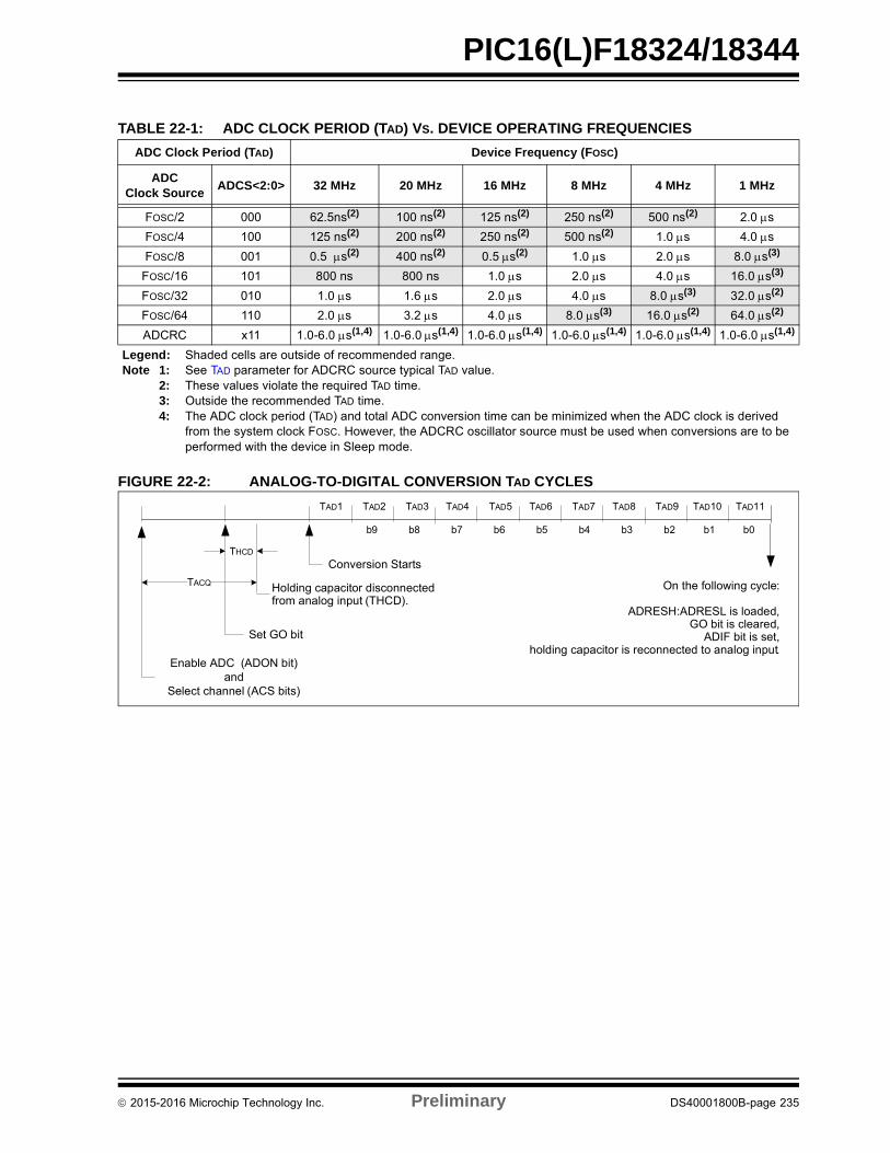
PIC16(L)F18324/18344
FIGURE 22-2: ANALOG-TO-DIGITAL CONVERSION TAD CYCLES
TABLE 22-1: ADC CLOCK PERIOD (TAD) VS. DEVICE OPERATING FREQUENCIES
ADC Clock Period (TAD) Device Frequency (FOSC)
ADCClock Source
ADCS<2:0> 32 MHz 20 MHz 16 MHz 8 MHz 4 MHz 1 MHz
FOSC/2 000 62.5ns(2) 100 ns(2) 125 ns(2) 250 ns(2) 500 ns(2) 2.0 s
FOSC/4 100 125 ns(2) 200 ns(2) 250 ns(2) 500 ns(2) 1.0 s 4.0 s
FOSC/8 001 0.5 s(2) 400 ns(2) 0.5 s(2) 1.0 s 2.0 s 8.0 s(3)
FOSC/16 101 800 ns 800 ns 1.0 s 2.0 s 4.0 s 16.0 s(3)
FOSC/32 010 1.0 s 1.6 s 2.0 s 4.0 s 8.0 s(3) 32.0 s(2)
FOSC/64 110 2.0 s 3.2 s 4.0 s 8.0 s(3) 16.0 s(2) 64.0 s(2)
ADCRC x11 1.0-6.0 s(1,4) 1.0-6.0 s(1,4) 1.0-6.0 s(1,4) 1.0-6.0 s(1,4) 1.0-6.0 s(1,4) 1.0-6.0 s(1,4)
Legend: Shaded cells are outside of recommended range.Note 1: See TAD parameter for ADCRC source typical TAD value.
2: These values violate the required TAD time.3: Outside the recommended TAD time.4: The ADC clock period (TAD) and total ADC conversion time can be minimized when the ADC clock is derived
from the system clock FOSC. However, the ADCRC oscillator source must be used when conversions are to be performed with the device in Sleep mode.
TAD1 TAD2 TAD3 TAD4 TAD5 TAD6 TAD7 TAD8 TAD9 TAD10 TAD11
Set GO bit
Conversion Starts
Holding capacitor disconnected from analog input (THCD).
On the following cycle:
ADRESH:ADRESL is loaded,GO bit is cleared,
ADIF bit is set,holding capacitor is reconnected to analog input.
b9 b8 b7 b6 b5 b4 b3 b2 b1 b0
Enable ADC (ADON bit)and
Select channel (ACS bits)
THCD
TACQ
2015-2016 Microchip Technology Inc. Preliminary DS40001800B-page 235
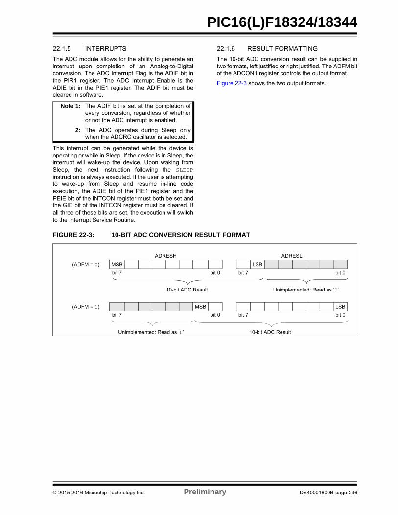
PIC16(L)F18324/18344
22.1.5 INTERRUPTS
The ADC module allows for the ability to generate aninterrupt upon completion of an Analog-to-Digitalconversion. The ADC Interrupt Flag is the ADIF bit inthe PIR1 register. The ADC Interrupt Enable is theADIE bit in the PIE1 register. The ADIF bit must becleared in software.
This interrupt can be generated while the device isoperating or while in Sleep. If the device is in Sleep, theinterrupt will wake-up the device. Upon waking fromSleep, the next instruction following the SLEEPinstruction is always executed. If the user is attemptingto wake-up from Sleep and resume in-line codeexecution, the ADIE bit of the PIE1 register and thePEIE bit of the INTCON register must both be set andthe GIE bit of the INTCON register must be cleared. Ifall three of these bits are set, the execution will switchto the Interrupt Service Routine.
22.1.6 RESULT FORMATTING
The 10-bit ADC conversion result can be supplied intwo formats, left justified or right justified. The ADFM bitof the ADCON1 register controls the output format.
Figure 22-3 shows the two output formats.
FIGURE 22-3: 10-BIT ADC CONVERSION RESULT FORMAT
Note 1: The ADIF bit is set at the completion ofevery conversion, regardless of whetheror not the ADC interrupt is enabled.
2: The ADC operates during Sleep onlywhen the ADCRC oscillator is selected.
ADRESH ADRESL
(ADFM = 0) MSB LSB
bit 7 bit 0 bit 7 bit 0
10-bit ADC Result Unimplemented: Read as ‘0’
(ADFM = 1) MSB LSB
bit 7 bit 0 bit 7 bit 0
Unimplemented: Read as ‘0’ 10-bit ADC Result
2015-2016 Microchip Technology Inc. Preliminary DS40001800B-page 236
PIC16(L)F18324/18344
22.2 ADC Operation
22.2.1 STARTING A CONVERSION
To enable the ADC module, the ADON bit of theADCON0 register must be set to a ‘1’. Setting theGO/DONE bit of the ADCON0 register to a ‘1’ will startthe Analog-to-Digital conversion.
22.2.2 COMPLETION OF A CONVERSION
When the conversion is complete, the ADC module will:
• Clear the GO/DONE bit
• Set the ADIF Interrupt Flag bit
• Update the ADRESH and ADRESL registers with new conversion result
22.2.3 TERMINATING A CONVERSION
If a conversion must be terminated before completion,the GO/DONE bit can be cleared in software. TheADRESH and ADRESL registers will be updated withthe partially complete Analog-to-Digital conversionsample. Incomplete bits will match the last bitconverted.
22.2.4 ADC OPERATION DURING SLEEP
The ADC module can operate during Sleep. Thisrequires the ADC clock source to be set to the ADCRCoption. When the ADCRC oscillator source is selected,the ADC waits one additional instruction before startingthe conversion. This allows the SLEEP instruction to beexecuted, which can reduce system noise during theconversion. If the ADC interrupt is enabled, the devicewill wake-up from Sleep when the conversioncompletes. If the ADC interrupt is disabled, the ADCmodule is turned off after the conversion completes,although the ADON bit remains set.
When the ADC clock source is something other thanADCRC, a SLEEP instruction causes the presentconversion to be aborted and the ADC module isturned off, although the ADON bit remains set.
22.2.5 AUTO-CONVERSION TRIGGER
The Auto-conversion Trigger allows periodic ADCmeasurements without software intervention. When arising edge of the selected source occurs, theGO/DONE bit is set by hardware.
The Auto-conversion Trigger source is selected withthe ADACT<4:0> bits of the ADACT register.
See Table 22-2 for auto-conversion sources.
Note: The GO/DONE bit should not be set in thesame instruction that turns on the ADC.Refer to Section 22.2.6 “ADC Conver-sion Procedure”.
Note: A device Reset forces all registers to theirReset state. Thus, the ADC module isturned off and any pending conversion isterminated.
TABLE 22-2: ADC AUTO-CONVERSION TABLE
Source Peripheral
Description
TMR0 Timer0 Overflow condition
TMR1 Timer1 Overflow condition
TMR3 Timer3 Overflow condition
TMR5 Timer5 Overflow condition
TMR2 Match between Timer2 and PR2
TMR4 Match between Timer4 and PR4
TMR6 Match between Timer6 and PR6
C1 Comparator C1 output
C2 Comparator C2 output
CLC1 CLC1 output
CLC2 CLC2 output
CLC3 CLC3 output
CLC4 CLC4 output
CCP1 CCP1 output
CCP2 CCP2 output
CCP3 CCP3 output
CCP4 CCP4 output
2015-2016 Microchip Technology Inc. Preliminary DS40001800B-page 237
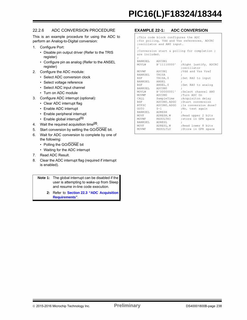
PIC16(L)F18324/18344
22.2.6 ADC CONVERSION PROCEDURE
This is an example procedure for using the ADC toperform an Analog-to-Digital conversion:
1. Configure Port:
• Disable pin output driver (Refer to the TRIS register)
• Configure pin as analog (Refer to the ANSEL register)
2. Configure the ADC module:
• Select ADC conversion clock
• Select voltage reference
• Select ADC input channel
• Turn on ADC module
3. Configure ADC interrupt (optional):
• Clear ADC interrupt flag
• Enable ADC interrupt
• Enable peripheral interrupt
• Enable global interrupt(1)
4. Wait the required acquisition time(2).
5. Start conversion by setting the GO/DONE bit.
6. Wait for ADC conversion to complete by one ofthe following:
• Polling the GO/DONE bit
• Waiting for the ADC interrupt
7. Read ADC Result.
8. Clear the ADC interrupt flag (required if interruptis enabled).
EXAMPLE 22-1: ADC CONVERSION
Note 1: The global interrupt can be disabled if theuser is attempting to wake-up from Sleepand resume in-line code execution.
2: Refer to Section 22.3 “ADC AcquisitionRequirements”.
;This code block configures the ADC;for polling, Vdd and Vss references, ADCRC ;oscillator and AN0 input.;;Conversion start & polling for completion ; are included.;BANKSEL ADCON1 ;MOVLW B’11110000’ ;Right justify, ADCRC
;oscillatorMOVWF ADCON1 ;Vdd and Vss VrefBANKSEL TRISA ;BSF TRISA,0 ;Set RA0 to inputBANKSEL ANSEL ;BSF ANSEL,0 ;Set RA0 to analogBANKSEL ADCON0 ;MOVLW B’00000001’ ;Select channel AN0MOVWF ADCON0 ;Turn ADC OnCALL SampleTime ;Acquisiton delayBSF ADCON0,ADGO ;Start conversionBTFSC ADCON0,ADGO ;Is conversion done?GOTO $-1 ;No, test againBANKSEL ADRESH ;MOVF ADRESH,W ;Read upper 2 bitsMOVWF RESULTHI ;store in GPR spaceBANKSEL ADRESL ;MOVF ADRESL,W ;Read lower 8 bitsMOVWF RESULTLO ;Store in GPR space
2015-2016 Microchip Technology Inc. Preliminary DS40001800B-page 238
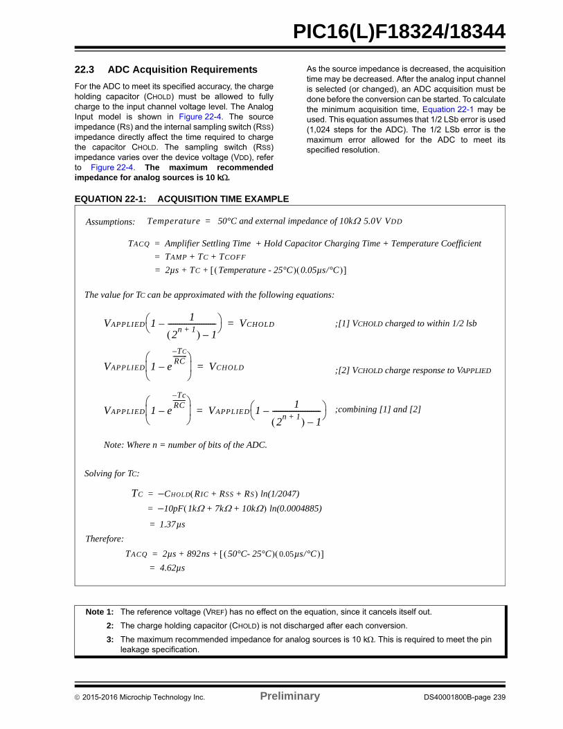
PIC16(L)F18324/18344
22.3 ADC Acquisition Requirements
For the ADC to meet its specified accuracy, the chargeholding capacitor (CHOLD) must be allowed to fullycharge to the input channel voltage level. The AnalogInput model is shown in Figure 22-4. The sourceimpedance (RS) and the internal sampling switch (RSS)impedance directly affect the time required to chargethe capacitor CHOLD. The sampling switch (RSS)impedance varies over the device voltage (VDD), referto Figure 22-4. The maximum recommendedimpedance for analog sources is 10 k.
As the source impedance is decreased, the acquisitiontime may be decreased. After the analog input channelis selected (or changed), an ADC acquisition must bedone before the conversion can be started. To calculatethe minimum acquisition time, Equation 22-1 may beused. This equation assumes that 1/2 LSb error is used(1,024 steps for the ADC). The 1/2 LSb error is themaximum error allowed for the ADC to meet itsspecified resolution.
EQUATION 22-1: ACQUISITION TIME EXAMPLE
Note 1: The reference voltage (VREF) has no effect on the equation, since it cancels itself out.
2: The charge holding capacitor (CHOLD) is not discharged after each conversion.
3: The maximum recommended impedance for analog sources is 10 k. This is required to meet the pin leakage specification.
TACQ Amplifier Settling Time Hold Capacitor Charging Time Temperature Coefficient+ +=
TAMP TC TCOFF+ +=
2µs TC Temperature - 25°C 0.05µs/°C + +=
TC CHOLD RIC RSS RS+ + ln(1/2047)–=
10pF 1k 7k 10k+ + – ln(0.0004885)=
1.37= µs
VAPPLIED 1 e
Tc–RC---------
–
VAPPLIED 11
2n 1+ 1–
--------------------------– =
VAPPLIED 11
2n 1+ 1–
--------------------------– VCHOLD=
VAPPLIED 1 e
TC–RC----------
–
VCHOLD=
;[1] VCHOLD charged to within 1/2 lsb
;[2] VCHOLD charge response to VAPPLIED
;combining [1] and [2]
The value for TC can be approximated with the following equations:
Solving for TC:
Therefore:
Temperature 50°C and external impedance of 10k 5.0V VDD=Assumptions:
Note: Where n = number of bits of the ADC.
TACQ 2µs 892ns 50°C- 25°C 0.05µs/°C + +=
4.62µs=
2015-2016 Microchip Technology Inc. Preliminary DS40001800B-page 239
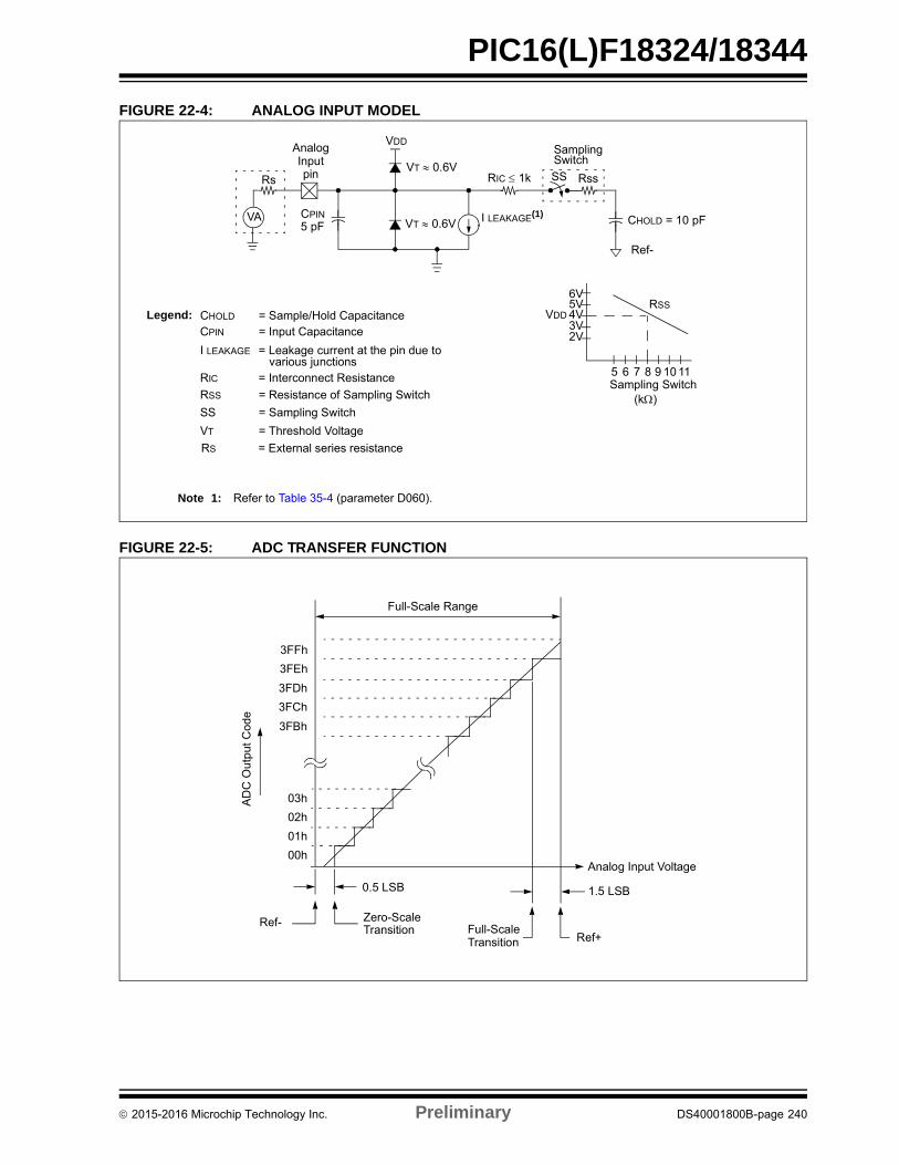
PIC16(L)F18324/18344
FIGURE 22-4: ANALOG INPUT MODEL
FIGURE 22-5: ADC TRANSFER FUNCTION
CPINVA
Rs
Analog
5 pF
VDD
VT 0.6V
VT 0.6V I LEAKAGE(1)
RIC 1k
SamplingSwitch
SS Rss
CHOLD = 10 pF
Ref-
6V
Sampling Switch
5V4V3V2V
5 6 7 8 9 10 11
(k)
VDD
Legend:
CPIN
VT
I LEAKAGE
RIC
SS
CHOLD
= Input Capacitance
= Threshold Voltage
= Leakage current at the pin due to
= Interconnect Resistance
= Sampling Switch
= Sample/Hold Capacitance
various junctions
RSS
Note 1: Refer to Table 35-4 (parameter D060).
RSS = Resistance of Sampling Switch
Inputpin
RS = External series resistance
3FFh
3FEh
AD
C O
utp
ut
Co
de
3FDh
3FCh
03h
02h
01h
00h
Full-Scale
3FBh
0.5 LSB
Ref- Zero-ScaleTransition
Ref+Transition
1.5 LSB
Full-Scale Range
Analog Input Voltage
2015-2016 Microchip Technology Inc. Preliminary DS40001800B-page 240
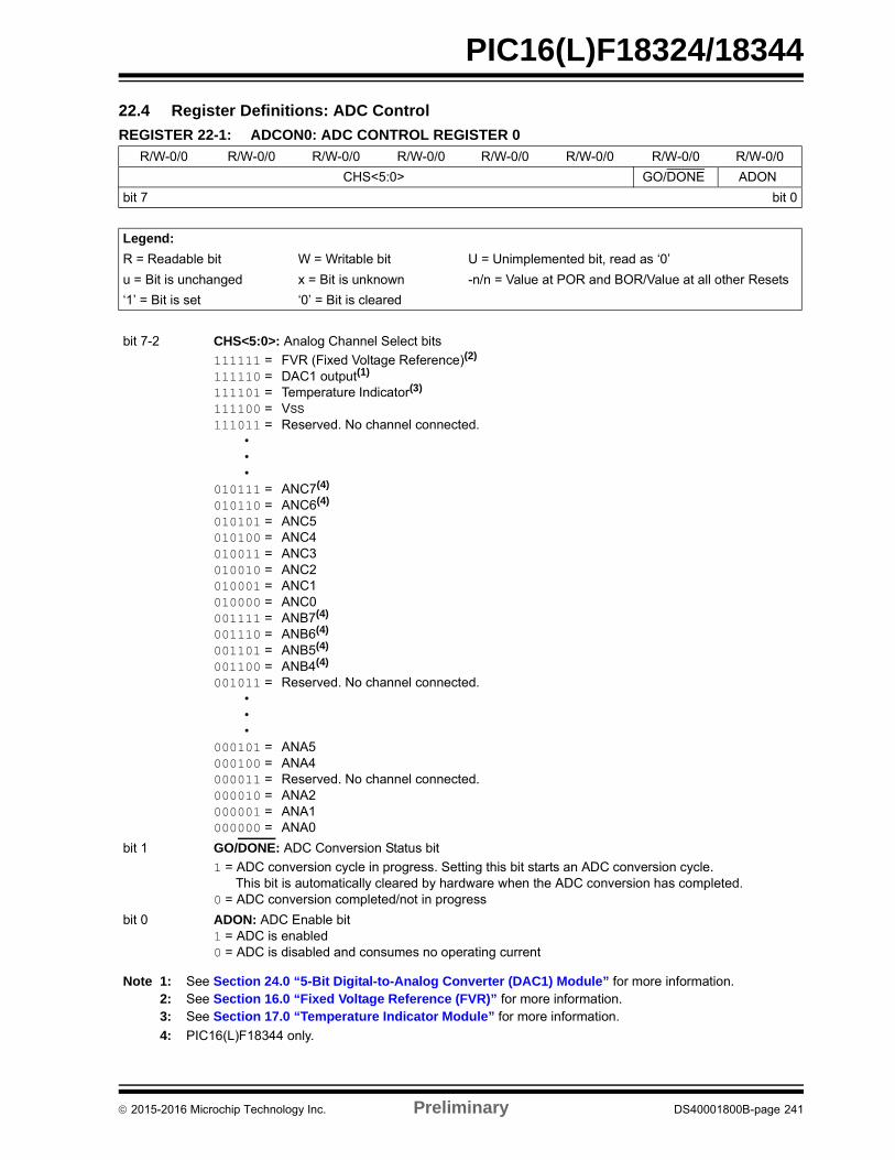
PIC16(L)F18324/18344
22.4 Register Definitions: ADC Control
REGISTER 22-1: ADCON0: ADC CONTROL REGISTER 0
R/W-0/0 R/W-0/0 R/W-0/0 R/W-0/0 R/W-0/0 R/W-0/0 R/W-0/0 R/W-0/0
CHS<5:0> GO/DONE ADON
bit 7 bit 0
Legend:
R = Readable bit W = Writable bit U = Unimplemented bit, read as ‘0’
u = Bit is unchanged x = Bit is unknown -n/n = Value at POR and BOR/Value at all other Resets
‘1’ = Bit is set ‘0’ = Bit is cleared
bit 7-2 CHS<5:0>: Analog Channel Select bits
111111 = FVR (Fixed Voltage Reference)(2)
111110 = DAC1 output(1)
111101 = Temperature Indicator(3)
111100 = VSS
111011 = Reserved. No channel connected. • • •
010111 = ANC7(4)
010110 = ANC6(4)
010101 = ANC5010100 = ANC4010011 = ANC3010010 = ANC2010001 = ANC1010000 = ANC0001111 = ANB7(4)
001110 = ANB6(4)
001101 = ANB5(4)
001100 = ANB4(4)
001011 = Reserved. No channel connected. • • •
000101 = ANA5000100 = ANA4000011 = Reserved. No channel connected.000010 = ANA2000001 = ANA1000000 = ANA0
bit 1 GO/DONE: ADC Conversion Status bit
1 = ADC conversion cycle in progress. Setting this bit starts an ADC conversion cycle. This bit is automatically cleared by hardware when the ADC conversion has completed.0 = ADC conversion completed/not in progress
bit 0 ADON: ADC Enable bit1 = ADC is enabled0 = ADC is disabled and consumes no operating current
Note 1: See Section 24.0 “5-Bit Digital-to-Analog Converter (DAC1) Module” for more information.2: See Section 16.0 “Fixed Voltage Reference (FVR)” for more information.3: See Section 17.0 “Temperature Indicator Module” for more information.
4: PIC16(L)F18344 only.
2015-2016 Microchip Technology Inc. Preliminary DS40001800B-page 241
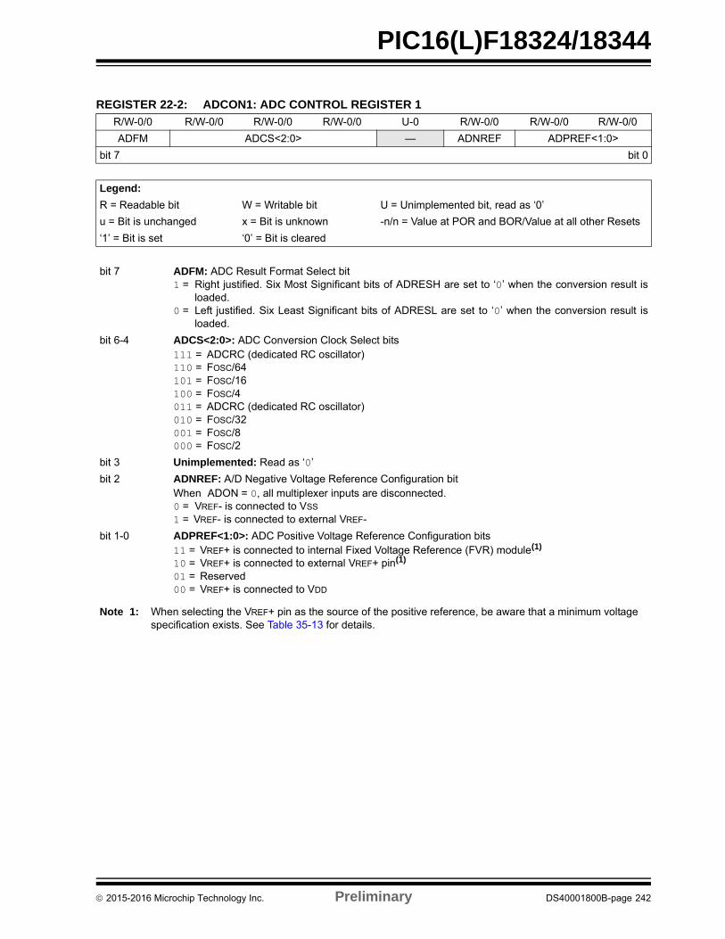
PIC16(L)F18324/18344
REGISTER 22-2: ADCON1: ADC CONTROL REGISTER 1
R/W-0/0 R/W-0/0 R/W-0/0 R/W-0/0 U-0 R/W-0/0 R/W-0/0 R/W-0/0
ADFM ADCS<2:0> — ADNREF ADPREF<1:0>
bit 7 bit 0
Legend:
R = Readable bit W = Writable bit U = Unimplemented bit, read as ‘0’
u = Bit is unchanged x = Bit is unknown -n/n = Value at POR and BOR/Value at all other Resets
‘1’ = Bit is set ‘0’ = Bit is cleared
bit 7 ADFM: ADC Result Format Select bit1 = Right justified. Six Most Significant bits of ADRESH are set to ‘0’ when the conversion result is
loaded.0 = Left justified. Six Least Significant bits of ADRESL are set to ‘0’ when the conversion result is
loaded.
bit 6-4 ADCS<2:0>: ADC Conversion Clock Select bits111 = ADCRC (dedicated RC oscillator)110 = FOSC/64101 = FOSC/16100 = FOSC/4011 = ADCRC (dedicated RC oscillator)010 = FOSC/32001 = FOSC/8000 = FOSC/2
bit 3 Unimplemented: Read as ‘0’
bit 2 ADNREF: A/D Negative Voltage Reference Configuration bitWhen ADON = 0, all multiplexer inputs are disconnected. 0 = VREF- is connected to VSS
1 = VREF- is connected to external VREF-
bit 1-0 ADPREF<1:0>: ADC Positive Voltage Reference Configuration bits11 = VREF+ is connected to internal Fixed Voltage Reference (FVR) module(1)
10 = VREF+ is connected to external VREF+ pin(1)
01 = Reserved00 = VREF+ is connected to VDD
Note 1: When selecting the VREF+ pin as the source of the positive reference, be aware that a minimum voltage specification exists. See Table 35-13 for details.
2015-2016 Microchip Technology Inc. Preliminary DS40001800B-page 242

PIC16(L)F18324/18344
REGISTER 22-3: ADACT: A/D AUTO-CONVERSION TRIGGER
U-0 U-0 U-0 R/W-0/0 R/W-0/0 R/W-0/0 R/W-0/0 R/W-0/0
— — — ADACT<4:0>
bit 7 bit 0
Legend:
R = Readable bit W = Writable bit U = Unimplemented bit, read as ‘0’
u = Bit is unchanged x = Bit is unknown -n/n = Value at POR and BOR/Value at all other Resets
‘1’ = Bit is set ‘0’ = Bit is cleared
bit 7-5 Unimplemented: Read as ‘0’
bit 4-0 ADACT<4:0>: Auto-Conversion Trigger Selection bits(1)
10001 = Timer5 overflow(2)
10000 = Timer3 overflow(2)
1111 = CCP41110 = CCP31101 = CCP21100 = CCP11011 = CLC41010 = CLC31001 = CLC21000 = CLC10111 = Comparator C20110 = Comparator C10101 = Timer2-PR2 match0100 = Timer1 overflow(2)
0011 = Timer0 overflow(2)
0010 = Timer6-PR6 match0001 = Timer4-PR4 match0000 = No auto-conversion trigger selected
Note 1: This is a rising edge sensitive input for all sources.
2: Trigger corresponds to when the peripheral’s interrupt flag is set.
2015-2016 Microchip Technology Inc. Preliminary DS40001800B-page 243
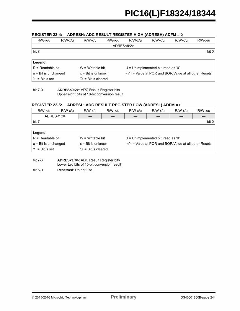
PIC16(L)F18324/18344
REGISTER 22-4: ADRESH: ADC RESULT REGISTER HIGH (ADRESH) ADFM = 0
R/W-x/u R/W-x/u R/W-x/u R/W-x/u R/W-x/u R/W-x/u R/W-x/u R/W-x/u
ADRES<9:2>
bit 7 bit 0
Legend:
R = Readable bit W = Writable bit U = Unimplemented bit, read as ‘0’
u = Bit is unchanged x = Bit is unknown -n/n = Value at POR and BOR/Value at all other Resets
‘1’ = Bit is set ‘0’ = Bit is cleared
bit 7-0 ADRES<9:2>: ADC Result Register bitsUpper eight bits of 10-bit conversion result
REGISTER 22-5: ADRESL: ADC RESULT REGISTER LOW (ADRESL) ADFM = 0
R/W-x/u R/W-x/u R/W-x/u R/W-x/u R/W-x/u R/W-x/u R/W-x/u R/W-x/u
ADRES<1:0> — — — — — —
bit 7 bit 0
Legend:
R = Readable bit W = Writable bit U = Unimplemented bit, read as ‘0’
u = Bit is unchanged x = Bit is unknown -n/n = Value at POR and BOR/Value at all other Resets
‘1’ = Bit is set ‘0’ = Bit is cleared
bit 7-6 ADRES<1:0>: ADC Result Register bitsLower two bits of 10-bit conversion result
bit 5-0 Reserved: Do not use.
2015-2016 Microchip Technology Inc. Preliminary DS40001800B-page 244
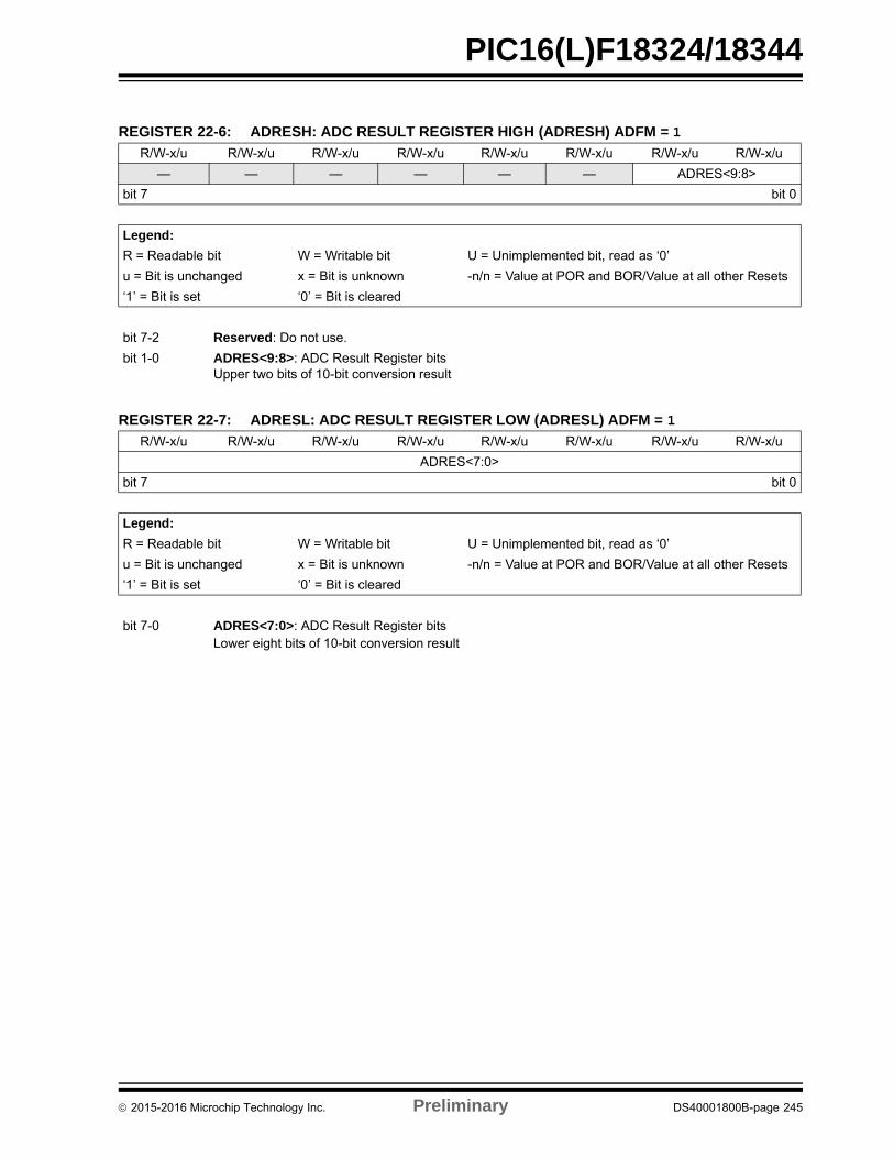
PIC16(L)F18324/18344
REGISTER 22-6: ADRESH: ADC RESULT REGISTER HIGH (ADRESH) ADFM = 1
R/W-x/u R/W-x/u R/W-x/u R/W-x/u R/W-x/u R/W-x/u R/W-x/u R/W-x/u
— — — — — — ADRES<9:8>
bit 7 bit 0
Legend:
R = Readable bit W = Writable bit U = Unimplemented bit, read as ‘0’
u = Bit is unchanged x = Bit is unknown -n/n = Value at POR and BOR/Value at all other Resets
‘1’ = Bit is set ‘0’ = Bit is cleared
bit 7-2 Reserved: Do not use.
bit 1-0 ADRES<9:8>: ADC Result Register bitsUpper two bits of 10-bit conversion result
REGISTER 22-7: ADRESL: ADC RESULT REGISTER LOW (ADRESL) ADFM = 1
R/W-x/u R/W-x/u R/W-x/u R/W-x/u R/W-x/u R/W-x/u R/W-x/u R/W-x/u
ADRES<7:0>
bit 7 bit 0
Legend:
R = Readable bit W = Writable bit U = Unimplemented bit, read as ‘0’
u = Bit is unchanged x = Bit is unknown -n/n = Value at POR and BOR/Value at all other Resets
‘1’ = Bit is set ‘0’ = Bit is cleared
bit 7-0 ADRES<7:0>: ADC Result Register bitsLower eight bits of 10-bit conversion result
2015-2016 Microchip Technology Inc. Preliminary DS40001800B-page 245
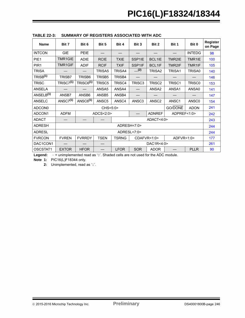
PIC16(L)F18324/18344
TABLE 22-3: SUMMARY OF REGISTERS ASSOCIATED WITH ADC
Name Bit 7 Bit 6 Bit 5 Bit 4 Bit 3 Bit 2 Bit 1 Bit 0Register on Page
INTCON GIE PEIE — — — — — INTEDG 98
PIE1 TMR1GIE ADIE RCIE TXIE SSP1IE BCL1IE TMR2IE TMR1IE 100
PIR1 TMR1GIF ADIF RCIF TXIF SSP1IF BCL1IF TMR2IF TMR1IF 105
TRISA — — TRISA5 TRISA4 —(2) TRISA2 TRISA1 TRISA0 140
TRISB(1) TRISB7 TRISB6 TRISB5 TRISB4 — — — — 146
TRISC TRISC7(1) TRISC6(1) TRISC5 TRISC4 TRISC3 TRISC2 TRISC1 TRISC0 153
ANSELA — — ANSA5 ANSA4 — ANSA2 ANSA1 ANSA0 141
ANSELB(1) ANSB7 ANSB6 ANSB5 ANSB4 — — — — 147
ANSELC ANSC7(1) ANSC6(1) ANSC5 ANSC4 ANSC3 ANSC2 ANSC1 ANSC0 154
ADCON0 CHS<5:0> GO/DONE ADON 241
ADCON1 ADFM ADCS<2:0> — ADNREF ADPREF<1:0> 242
ADACT — — — ADACT<4:0> 243
ADRESH ADRESH<7:0> 244
ADRESL ADRESL<7:0> 244
FVRCON FVREN FVRRDY TSEN TSRNG CDAFVR<1:0> ADFVR<1:0> 177
DAC1CON1 — — — DAC1R<4:0> 261
OSCSTAT1 EXTOR HFOR — LFOR SOR ADOR — PLLR 90
Legend: — = unimplemented read as ‘0’. Shaded cells are not used for the ADC module.Note 1: PIC16(L)F18344 only.
2: Unimplemented, read as ‘1’.
2015-2016 Microchip Technology Inc. Preliminary DS40001800B-page 246
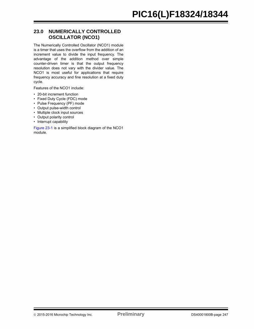
PIC16(L)F18324/18344
23.0 NUMERICALLY CONTROLLED OSCILLATOR (NCO1)
The Numerically Controlled Oscillator (NCO1) moduleis a timer that uses the overflow from the addition of anincrement value to divide the input frequency. Theadvantage of the addition method over simplecounter-driven timer is that the output frequencyresolution does not vary with the divider value. TheNCO1 is most useful for applications that requirefrequency accuracy and fine resolution at a fixed dutycycle.
Features of the NCO1 include:
• 20-bit increment function• Fixed Duty Cycle (FDC) mode• Pulse Frequency (PF) mode• Output pulse-width control• Multiple clock input sources• Output polarity control• Interrupt capability
Figure 23-1 is a simplified block diagram of the NCO1module.
2015-2016 Microchip Technology Inc. Preliminary DS40001800B-page 247
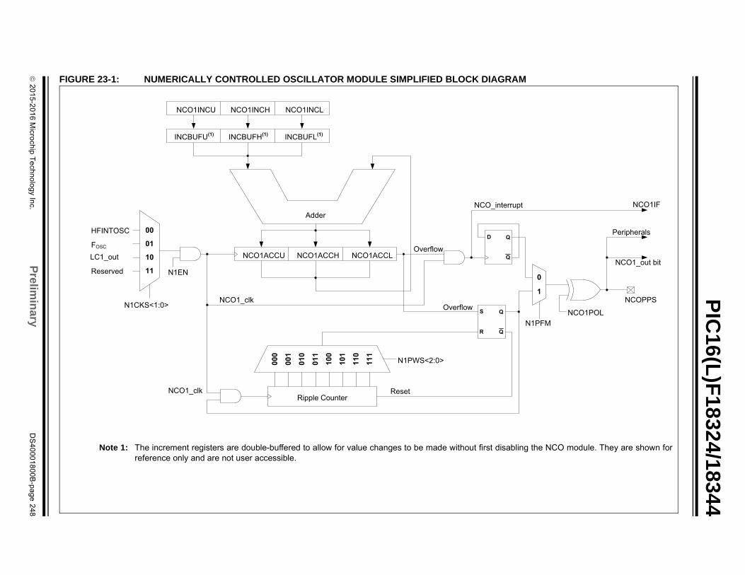
2
01
5-2
01
6 M
icroch
ip T
ech
no
log
y Inc.
Prelim
inary
DS
40
00
18
00
B-p
ag
e 2
48
PIC
16(L)F
18324/18344
FIG
the NCO module. They are shown for
1
0
POL
PPS
IF
bit
Peripherals
URE 23-1: NUMERICALLY CONTROLLED OSCILLATOR MODULE SIMPLIFIED BLOCK DIAGRAM
Note 1: The increment registers are double-buffered to allow for value changes to be made without first disablingreference only and are not user accessible.
00
11
10
01
000
011
010
001
100
101
110
111
R
S Q
Q
D Q
Q
INCU INCH INCL
INCBUFU(1) INCBUFH(1) INCBUFL(1)
ACCU ACCH ACCL
HFINTOSC
FOSC
LC1
CKS<1:0>
PWS<2:0>
Ripple Counter
Overflow
Overflow
Reset
EN
Addernterrupt
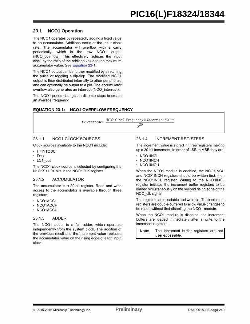
PIC16(L)F18324/18344
23.1 NCO1 Operation
The NCO1 operates by repeatedly adding a fixed valueto an accumulator. Additions occur at the input clockrate. The accumulator will overflow with a carryperiodically, which is the raw NCO1 output(NCO_overflow). This effectively reduces the inputclock by the ratio of the addition value to the maximumaccumulator value. See Equation 23-1.
The NCO1 output can be further modified by stretchingthe pulse or toggling a flip-flop. The modified NCO1output is then distributed internally to other peripheralsand can optionally be output to a pin. The accumulatoroverflow also generates an interrupt (NCO_interrupt).
The NCO1 period changes in discrete steps to createan average frequency.
EQUATION 23-1: NCO1 OVERFLOW FREQUENCY
23.1.1 NCO1 CLOCK SOURCES
Clock sources available to the NCO1 include:
• HFINTOSC• FOSC
• LC1_out
The NCO1 clock source is selected by configuring theN1CKS<1:0> bits in the NCO1CLK register.
23.1.2 ACCUMULATOR
The accumulator is a 20-bit register. Read and writeaccess to the accumulator is available through threeregisters:
• NCO1ACCL• NCO1ACCH• NCO1ACCU
23.1.3 ADDER
The NCO1 adder is a full adder, which operatesindependently from the system clock. The addition ofthe previous result and the increment value replacesthe accumulator value on the rising edge of each inputclock.
23.1.4 INCREMENT REGISTERS
The increment value is stored in three registers makingup a 20-bit increment. In order of LSB to MSB they are:
• NCO1INCL• NCO1INCH• NCO1INCU
When the NCO1 module is enabled, the NCO1INCUand NCO1INCH registers should be written first, thenthe NCO1INCL register. Writing to the NCO1INCLregister initiates the increment buffer registers to beloaded simultaneously on the second rising edge of theNCO_clk signal.
The registers are readable and writable. The incrementregisters are double-buffered to allow value changes tobe made without first disabling the NCO1 module.
When the NCO1 module is disabled, the incrementbuffers are loaded immediately after a write to theincrement registers.
FOVERFLOWNCO Clock Frequency Increment Value
220
----------------------------------------------------------------------------------------------------------------=
Note: The increment buffer registers are notuser-accessible.
2015-2016 Microchip Technology Inc. Preliminary DS40001800B-page 249
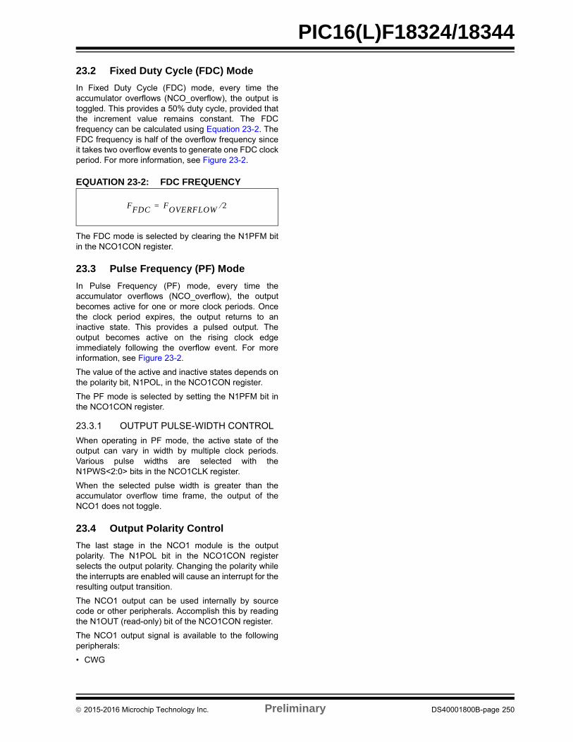
PIC16(L)F18324/18344
23.2 Fixed Duty Cycle (FDC) Mode
In Fixed Duty Cycle (FDC) mode, every time theaccumulator overflows (NCO_overflow), the output istoggled. This provides a 50% duty cycle, provided thatthe increment value remains constant. The FDCfrequency can be calculated using Equation 23-2. TheFDC frequency is half of the overflow frequency sinceit takes two overflow events to generate one FDC clockperiod. For more information, see Figure 23-2.
EQUATION 23-2: FDC FREQUENCY
The FDC mode is selected by clearing the N1PFM bitin the NCO1CON register.
23.3 Pulse Frequency (PF) Mode
In Pulse Frequency (PF) mode, every time theaccumulator overflows (NCO_overflow), the outputbecomes active for one or more clock periods. Oncethe clock period expires, the output returns to aninactive state. This provides a pulsed output. Theoutput becomes active on the rising clock edgeimmediately following the overflow event. For moreinformation, see Figure 23-2.
The value of the active and inactive states depends onthe polarity bit, N1POL, in the NCO1CON register.
The PF mode is selected by setting the N1PFM bit inthe NCO1CON register.
23.3.1 OUTPUT PULSE-WIDTH CONTROL
When operating in PF mode, the active state of theoutput can vary in width by multiple clock periods.Various pulse widths are selected with theN1PWS<2:0> bits in the NCO1CLK register.
When the selected pulse width is greater than theaccumulator overflow time frame, the output of theNCO1 does not toggle.
23.4 Output Polarity Control
The last stage in the NCO1 module is the outputpolarity. The N1POL bit in the NCO1CON registerselects the output polarity. Changing the polarity whilethe interrupts are enabled will cause an interrupt for theresulting output transition.
The NCO1 output can be used internally by sourcecode or other peripherals. Accomplish this by readingthe N1OUT (read-only) bit of the NCO1CON register.
The NCO1 output signal is available to the followingperipherals:
• CWG
FFDC FOVERFLOW 2=
2015-2016 Microchip Technology Inc. Preliminary DS40001800B-page 250
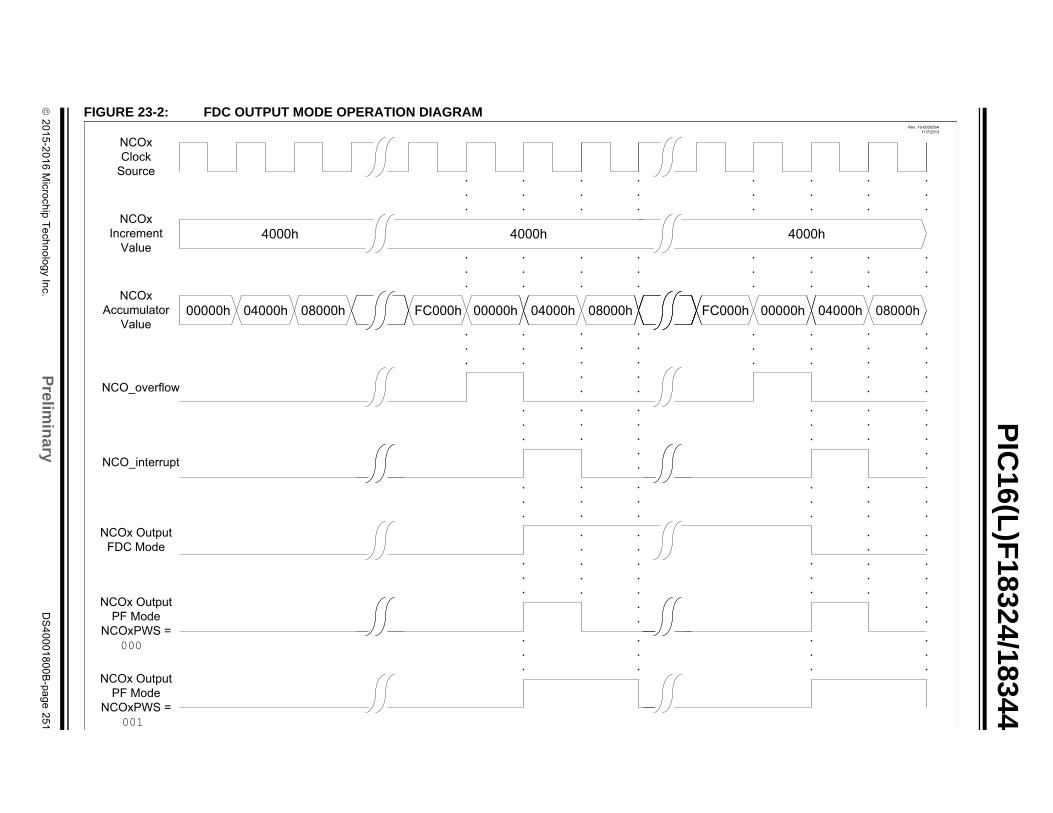
2
01
5-2
01
6 M
icroch
ip T
ech
no
log
y Inc.
Prelim
inary
DS
40
00
18
00
B-p
ag
e 2
51
PIC
16(L)F
18324/18344
FIGRev. 10-000029A
11/7/2013
00000h 04000h 08000h
4000h
URE 23-2: FDC OUTPUT MODE OPERATION DIAGRAM
00000h 04000h 08000h FC000h 00000h 04000h 08000h FC000h
4000h 4000h
NCO_interrupt
NCOx OutputFDC Mode
NCOx OutputPF Mode
NCOxPWS =
NCOx OutputPF Mode
NCOxPWS =
NCOxAccumulator
Value
NCOx Increment
Value
NCOx Clock
Source
000
001
NCO_overflow
PIC16(L)F18324/18344
23.5 Interrupts
When the accumulator overflows (NCO_overflow), theNCO1 Interrupt Flag bit, NCO1IF, of the PIR2 registeris set. To enable the interrupt event (NCO_interrupt),the following bits must be set:
• N1EN bit of the NCO1CON register• NCO1IE bit of the PIE2 register• PEIE bit of the INTCON register• GIE bit of the INTCON register
The interrupt must be cleared by software by clearingthe NCO1IF bit in the Interrupt Service Routine.
23.6 Effects of a Reset
All of the NCO1 registers are cleared to zero as theresult of a Reset.
23.7 Operation in Sleep
The NCO1 module operates independently from thesystem clock and will continue to run during Sleep,provided that the clock source selected remains active.
The HFINTOSC remains active during Sleep when theNCO1 module is enabled and the HFINTOSC isselected as the clock source, regardless of the systemclock source selected.
In other words, if the HFINTOSC is simultaneouslyselected as the system clock and the NCO1 clocksource, when the NCO1 is enabled, the CPU will goidle during Sleep, but the NCO1 will continue to operateand the HFINTOSC will remain active.
This will have a direct effect on the Sleep mode current.
2015-2016 Microchip Technology Inc. Preliminary DS40001800B-page 252
PIC16(L)F18324/18344
23.8 NCO1 Control Registers
REGISTER 23-1: NCO1CON: NCO1 CONTROL REGISTER
R/W-0/0 U-0 R-0/0 R/W-0/0 U-0 U-0 U-0 R/W-0/0
N1EN — N1OUT N1POL — — — N1PFM
bit 7 bit 0
Legend:
R = Readable bit W = Writable bit U = Unimplemented bit, read as ‘0’
u = Bit is unchanged x = Bit is unknown -n/n = Value at POR and BOR/Value at all other Resets
‘1’ = Bit is set ‘0’ = Bit is cleared
bit 7 N1EN: NCO1 Enable bit1 = NCO1 module is enabled0 = NCO1 module is disabled
bit 6 Unimplemented: Read as ‘0’
bit 5 N1OUT: NCO1 Output bitDisplays the current output value of the NCO1 module
bit 4 N1POL: NCO1 Polarity1 = NCO1 output signal is inverted0 = NCO1 output signal is not inverted
bit 3-1 Unimplemented: Read as ‘0’.
bit 0 N1PFM: NCO1 Output Divider mode1 = NCO1 operates in Pulse Frequency mode0 = NCO1 operates in Fixed Duty Cycle mode, divide by 2
2015-2016 Microchip Technology Inc. Preliminary DS40001800B-page 253
PIC16(L)F18324/18344
REGISTER 23-2: NCO1CLK: NCO1 INPUT CLOCK CONTROL REGISTER
R/W-0/0 R/W-0/0 R/W-0/0 U-0 U-0 U-0 R/W-0/0 R/W-0/0
N1PWS<2:0> — — — N1CKS<1:0>
bit 7 bit 0
Legend:
R = Readable bit W = Writable bit U = Unimplemented bit, read as ‘0’
u = Bit is unchanged x = Bit is unknown -n/n = Value at POR and BOR/Value at all other Resets
‘1’ = Bit is set ‘0’ = Bit is cleared
bit 7-5 N1PWS<2:0>: NCO1 Output Pulse-Width Select bits(1, 2)
000 = NCO1 output is active for 1 input clock period001 = NCO1 output is active for 2 input clock periods010 = NCO1 output is active for 4 input clock periods011 = NCO1 output is active for 8 input clock periods100 = NCO1 output is active for 16 input clock periods101 = NCO1 output is active for 32 input clock periods110 = NCO1 output is active for 64 input clock periods111 = NCO1 output is active for 128 input clock periods
bit 4-2 Unimplemented: Read as ‘0’
bit 1-0 N1CKS<1:0>: NCO1 Clock Source Select bits00 = HFINTOSC (16 MHz)01 = FOSC
10 = CLC1OUT11 =Reserved
Note 1: N1PWS applies only when operating in Pulse Frequency mode.
2: If NCO pulse width is greater than NCO overflow period, the NCO1 output does not toggle.
REGISTER 23-3: NCO1ACCL: NCO1 ACCUMULATOR REGISTER – LOW BYTE
R/W-0/0 R/W-0/0 R/W-0/0 R/W-0/0 R/W-0/0 R/W-0/0 R/W-0/0 R/W-0/0
NCO1ACC<7:0>
bit 7 bit 0
Legend:
R = Readable bit W = Writable bit U = Unimplemented bit, read as ‘0’
u = Bit is unchanged x = Bit is unknown -n/n = Value at POR and BOR/Value at all other Resets
‘1’ = Bit is set ‘0’ = Bit is cleared
bit 7-0 NCO1ACC<7:0>: NCO1 Accumulator, low byte
2015-2016 Microchip Technology Inc. Preliminary DS40001800B-page 254
PIC16(L)F18324/18344
REGISTER 23-4: NCO1ACCH: NCO1 ACCUMULATOR REGISTER – HIGH BYTE
R/W-0/0 R/W-0/0 R/W-0/0 R/W-0/0 R/W-0/0 R/W-0/0 R/W-0/0 R/W-0/0
NCO1ACC<15:8>
bit 7 bit 0
Legend:
R = Readable bit W = Writable bit U = Unimplemented bit, read as ‘0’
u = Bit is unchanged x = Bit is unknown -n/n = Value at POR and BOR/Value at all other Resets
‘1’ = Bit is set ‘0’ = Bit is cleared
bit 7-0 NCO1ACC<15:8>: NCO1 Accumulator, high byte
REGISTER 23-5: NCO1ACCU: NCO1 ACCUMULATOR REGISTER – UPPER BYTE(1)
U-0 U-0 U-0 U-0 R/W-0/0 R/W-0/0 R/W-0/0 R/W-0/0
— — — — NCO1ACC<19:16>
bit 7 bit 0
Legend:
R = Readable bit W = Writable bit U = Unimplemented bit, read as ‘0’
u = Bit is unchanged x = Bit is unknown -n/n = Value at POR and BOR/Value at all other Resets
‘1’ = Bit is set ‘0’ = Bit is cleared
bit 7-4 Unimplemented: Read as ‘0’
bit 3-0 NCO1ACC<19:16>: NCO1 Accumulator, upper byte
Note 1: The accumulator spans registers NCO1ACCU:NCO1ACCH:NCO1ACCL. The 24 bits are reserved but not all are used.This register updates in real-time, asynchronously to the CPU; there is no provision to guarantee atomic access to this 24-bit space using an 8-bit bus. Writing to this register while the module is operating will produce undefined results.
REGISTER 23-6: NCO1INCL(1,2): NCO1 INCREMENT REGISTER – LOW BYTE
R/W-0/0 R/W-0/0 R/W-0/0 R/W-0/0 R/W-0/0 R/W-0/0 R/W-0/0 R/W-1/1
NCO1INC<7:0>
bit 7 bit 0
Legend:
R = Readable bit W = Writable bit U = Unimplemented bit, read as ‘0’
u = Bit is unchanged x = Bit is unknown -n/n = Value at POR and BOR/Value at all other Resets
‘1’ = Bit is set ‘0’ = Bit is cleared
bit 7-0 NCO1INC<7:0>: NCO1 Increment, low byte
Note 1: The logical increment spans NCO1INCU:NCO1INCH:NCO1INCL.2: NCO1INC is double-buffered as INCBUF; INCBUF is updated on the next falling edge of NCOCLK after
writing to NCO1INCL;NCO1INCU and NCO1INCH should be written prior to writing NCO1INCL.
2015-2016 Microchip Technology Inc. Preliminary DS40001800B-page 255
PIC16(L)F18324/18344
REGISTER 23-7: NCO1INCH(1): NCO1 INCREMENT REGISTER – HIGH BYTE
R/W-0/0 R/W-0/0 R/W-0/0 R/W-0/0 R/W-0/0 R/W-0/0 R/W-0/0 R/W-0/0
NCO1INC<15:8>
bit 7 bit 0
Legend:
R = Readable bit W = Writable bit U = Unimplemented bit, read as ‘0’
u = Bit is unchanged x = Bit is unknown -n/n = Value at POR and BOR/Value at all other Resets
‘1’ = Bit is set ‘0’ = Bit is cleared
bit 7-0 NCO1INC<15:8>: NCO1 Increment, high byte
Note 1: The logical increment spans NCO1INCU:NCO1INCH:NCO1INCL.
REGISTER 23-8: NCO1INCU(1): NCO1 INCREMENT REGISTER – UPPER BYTE
U-0 U-0 U-0 U-0 R/W-0/0 R/W-0/0 R/W-0/0 R/W-0/0
— — — — NCO1INC<19:16>
bit 7 bit 0
Legend:
R = Readable bit W = Writable bit U = Unimplemented bit, read as ‘0’
u = Bit is unchanged x = Bit is unknown -n/n = Value at POR and BOR/Value at all other Resets
‘1’ = Bit is set ‘0’ = Bit is cleared
bit 7-4 Unimplemented: Read as ‘0’
bit 3-0 NCO1INC<19:16>: NCO1 Increment, upper byte
Note 1: The logical increment spans NCO1INCU:NCO1INCH:NCO1INCL.
2015-2016 Microchip Technology Inc. Preliminary DS40001800B-page 256
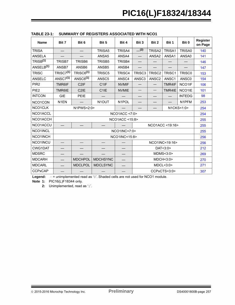
PIC16(L)F18324/18344
TABLE 23-1: SUMMARY OF REGISTERS ASSOCIATED WITH NCO1
Name Bit 7 Bit 6 Bit 5 Bit 4 Bit 3 Bit 2 Bit 1 Bit 0Register on Page
TRISA — — TRISA5 TRISA4 —(2) TRISA2 TRISA1 TRISA0 140
ANSELA — — ANSA5 ANSA4 — ANSA2 ANSA1 ANSA0 141
TRISB(1) TRISB7 TRISB6 TRISB5 TRISB4 — — — — 146
ANSELB(1) ANSB7 ANSB6 ANSB5 ANSB4 — — — — 147
TRISC TRISC7(1) TRISC6(1) TRISC5 TRISC4 TRISC3 TRISC2 TRISC1 TRISC0 153
ANSELC ANSC7(1) ANSC6(1) ANSC5 ANSC4 ANSC3 ANSC2 ANSC1 ANSC0 154
PIR2 TMR6IF C2IF C1IF NVMIF ― ― TMR4IF NCO1IF 106
PIE2 TMR6IE C2IE C1IE NVMIE ― ― TMR4IE NCO1IE 101
INTCON GIE PEIE — — — — — INTEDG 98
NCO1CON N1EN — N1OUT N1POL — — — N1PFM 253
NCO1CLK N1PWS<2:0> — — — N1CKS<1:0> 254
NCO1ACCL NCO1ACC <7:0> 254
NCO1ACCH NCO1ACC <15:8> 255
NCO1ACCU — — — — NCO1ACC <19:16> 255
NCO1INCL NCO1INC<7:0> 255
NCO1INCH NCO1INC<15:8> 256
NCO1INCU — — — — NCO1INC<19:16> 256
CWG1DAT — — — — DAT<3:0> 212
MDSRC — — — — MDMS<3:0> 269
MDCARH — MDCHPOL MDCHSYNC — MDCH<3:0> 270
MDCARL — MDCLPOL MDCLSYNC — MDCL<3:0> 271
CCPxCAP — — — — CCPxCTS<3:0> 307
Legend: — = unimplemented read as ‘0’. Shaded cells are not used for NCO1 module.Note 1: PIC16(L)F18344 only.
2: Unimplemented, read as ‘1’.
2015-2016 Microchip Technology Inc. Preliminary DS40001800B-page 257
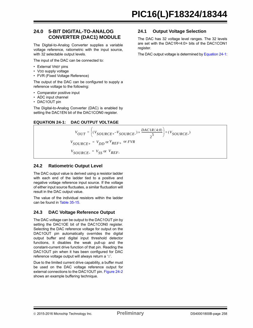
PIC16(L)F18324/18344
24.0 5-BIT DIGITAL-TO-ANALOG CONVERTER (DAC1) MODULE
The Digital-to-Analog Converter supplies a variablevoltage reference, ratiometric with the input source,with 32 selectable output levels.
The input of the DAC can be connected to:
• External VREF pins• VDD supply voltage• FVR (Fixed Voltage Reference)
The output of the DAC can be configured to supply areference voltage to the following:
• Comparator positive input• ADC input channel• DAC1OUT pin
The Digital-to-Analog Converter (DAC) is enabled bysetting the DAC1EN bit of the DAC1CON0 register.
24.1 Output Voltage Selection
The DAC has 32 voltage level ranges. The 32 levelsare set with the DAC1R<4:0> bits of the DAC1CON1register.
The DAC output voltage is determined by Equation 24-1:
EQUATION 24-1: DAC OUTPUT VOLTAGE
24.2 Ratiometric Output Level
The DAC output value is derived using a resistor ladderwith each end of the ladder tied to a positive andnegative voltage reference input source. If the voltageof either input source fluctuates, a similar fluctuation willresult in the DAC output value.
The value of the individual resistors within the laddercan be found in Table 35-15.
24.3 DAC Voltage Reference Output
The DAC voltage can be output to the DAC1OUT pin bysetting the DAC1OE bit of the DAC1CON0 register.Selecting the DAC reference voltage for output on theDAC1OUT pin automatically overrides the digitaloutput buffer and digital input threshold detectorfunctions, it disables the weak pull-up and theconstant-current drive function of that pin. Reading theDAC1OUT pin when it has been configured for DACreference voltage output will always return a ‘0’.
Due to the limited current drive capability, a buffer mustbe used on the DAC voltage reference output forexternal connections to the DAC1OUT pin. Figure 24-2shows an example buffering technique.
VOUT VSOURCE+ VSOURCE-– DAC1R 4:0
25
----------------------------------
VSOURCE- +=
VSOURCE+ VDD or=
VSOURCE- VSS or=
VREF+ or FVR
VREF-
2015-2016 Microchip Technology Inc. Preliminary DS40001800B-page 258
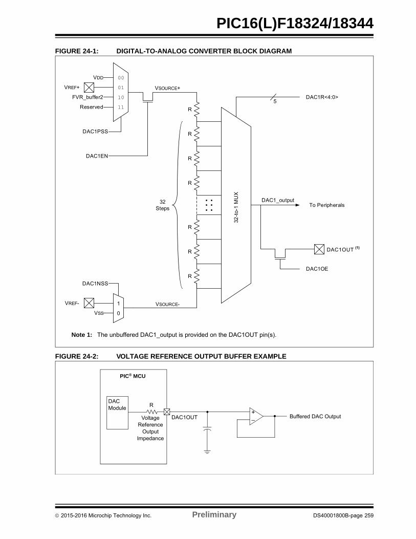
PIC16(L)F18324/18344
FIGURE 24-1: DIGITAL-TO-ANALOG CONVERTER BLOCK DIAGRAM
FIGURE 24-2: VOLTAGE REFERENCE OUTPUT BUFFER EXAMPLE
Note 1: The unbuffered DAC1_output is provided on the DAC1OUT pin(s).
VREF+
VDD
VSOURCE+
VSOURCE-VSS
R
32Steps
R
R
R
R
R
R
32-to
-1 M
UX
To Peripherals
DAC1OUT (1)
DAC1OE
DAC1_output
DAC1EN
DAC1R<4:0>5
00
111001
FVR_buffer2
Reserved
DAC1PSS
1
0
VREF-
DAC1NSS
DAC1OUT Buffered DAC Output+–
DACModule
Voltage Reference
Output Impedance
R
PIC® MCU
2015-2016 Microchip Technology Inc. Preliminary DS40001800B-page 259
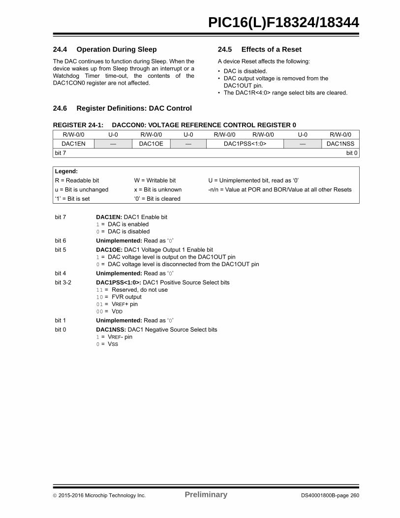
PIC16(L)F18324/18344
24.4 Operation During Sleep
The DAC continues to function during Sleep. When thedevice wakes up from Sleep through an interrupt or aWatchdog Timer time-out, the contents of theDAC1CON0 register are not affected.
24.5 Effects of a Reset
A device Reset affects the following:
• DAC is disabled.• DAC output voltage is removed from the
DAC1OUT pin.• The DAC1R<4:0> range select bits are cleared.
24.6 Register Definitions: DAC Control
REGISTER 24-1: DACCON0: VOLTAGE REFERENCE CONTROL REGISTER 0
R/W-0/0 U-0 R/W-0/0 U-0 R/W-0/0 R/W-0/0 U-0 R/W-0/0
DAC1EN — DAC1OE — DAC1PSS<1:0> — DAC1NSS
bit 7 bit 0
Legend:
R = Readable bit W = Writable bit U = Unimplemented bit, read as ‘0’
u = Bit is unchanged x = Bit is unknown -n/n = Value at POR and BOR/Value at all other Resets
‘1’ = Bit is set ‘0’ = Bit is cleared
bit 7 DAC1EN: DAC1 Enable bit1 = DAC is enabled0 = DAC is disabled
bit 6 Unimplemented: Read as ‘0’
bit 5 DAC1OE: DAC1 Voltage Output 1 Enable bit1 = DAC voltage level is output on the DAC1OUT pin0 = DAC voltage level is disconnected from the DAC1OUT pin
bit 4 Unimplemented: Read as ‘0’
bit 3-2 DAC1PSS<1:0>: DAC1 Positive Source Select bits11 = Reserved, do not use10 = FVR output01 = VREF+ pin00 = VDD
bit 1 Unimplemented: Read as ‘0’
bit 0 DAC1NSS: DAC1 Negative Source Select bits1 = VREF- pin0 = VSS
2015-2016 Microchip Technology Inc. Preliminary DS40001800B-page 260
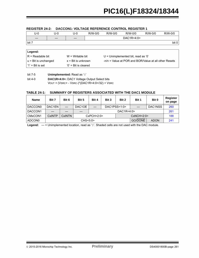
PIC16(L)F18324/18344
REGISTER 24-2: DACCON1: VOLTAGE REFERENCE CONTROL REGISTER 1
U-0 U-0 U-0 R/W-0/0 R/W-0/0 R/W-0/0 R/W-0/0 R/W-0/0
— — — DAC1R<4:0>
bit 7 bit 0
Legend:
R = Readable bit W = Writable bit U = Unimplemented bit, read as ‘0’
u = Bit is unchanged x = Bit is unknown -n/n = Value at POR and BOR/Value at all other Resets
‘1’ = Bit is set ‘0’ = Bit is cleared
bit 7-5 Unimplemented: Read as ‘0’
bit 4-0 DAC1R<4:0>: DAC1 Voltage Output Select bitsVOUT = (VSRC+ - VSRC-)*(DAC1R<4:0>/32) + VSRC
TABLE 24-1: SUMMARY OF REGISTERS ASSOCIATED WITH THE DAC1 MODULE
Name Bit 7 Bit 6 Bit 5 Bit 4 Bit 3 Bit 2 Bit 1 Bit 0Register on page
DACCON0 DAC1EN — DAC1OE — DAC1PSS<1:0> — DAC1NSS 260
DACCON1 — — — DAC1R<4:0> 261
CMxCON1 CxINTP CxINTN CxPCH<2:0> CxNCH<2:0> 188
ADCON0 CHS<5:0> GO/DONE ADON 241
Legend: — = Unimplemented location, read as ‘0’. Shaded cells are not used with the DAC module.
2015-2016 Microchip Technology Inc. Preliminary DS40001800B-page 261

PIC16(L)F18324/18344
25.0 DATA SIGNAL MODULATOR (DSM) MODULE
The Data Signal Modulator (DSM) is a peripheral whichallows the user to mix a data stream, also known as amodulator signal, with a carrier signal to produce amodulated output.
Both the carrier and the modulator signals are suppliedto the DSM module either internally from the output ofa peripheral, or externally through an input pin.
The modulated output signal is generated byperforming a logical “AND” operation of both the carrierand modulator signals and then provided to the MDOUTpin.
The carrier signal is comprised of two distinct andseparate signals. A carrier high (CARH) signal and acarrier low (CARL) signal. During the time in which themodulator (MOD) signal is in a logic-high state, theDSM mixes the carrier high signal with the modulatorsignal. When the modulator signal is in a logic-lowstate, the DSM mixes the carrier low signal with themodulator signal.
Using this method, the DSM can generate the followingtypes of Key Modulation schemes:
• Frequency-Shift Keying (FSK)• Phase-Shift Keying (PSK)• On-Off Keying (OOK)
Additionally, the following features are provided withinthe DSM module:
• Carrier Synchronization• Carrier Source Polarity Select• Carrier Source Pin Disable• Programmable Modulator Data• Modulator Source Pin Disable• Modulated Output Polarity Select• Slew Rate Control
Figure 25-1 shows a Simplified Block Diagram of theData Signal Modulator peripheral.
2015-2016 Microchip Technology Inc. Preliminary DS40001800B-page 262
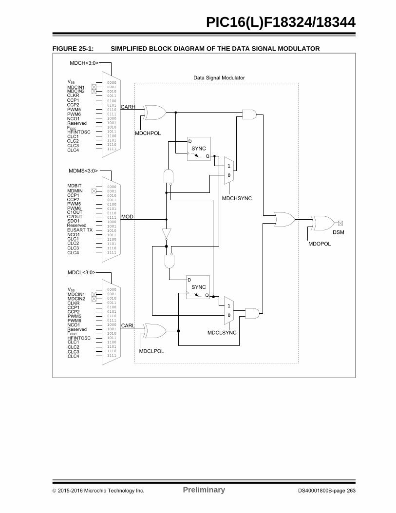
PIC16(L)F18324/18344
FIGURE 25-1: SIMPLIFIED BLOCK DIAGRAM OF THE DATA SIGNAL MODULATOR
D
Q
D
Q
SYNC
SYNC
DSM
MDOPOL
MDCHPOL
MDCLPOL
MDCLSYNC
MDCHSYNC
CARL
CARH
MOD
MDCH<3:0>
MDMS<3:0>
MDCL<3:0>
VSSMDCIN1MDCIN2CLKR
PWM5PWM6
RFOSCHFINTOSCCLC1CLC2CLC3CLC4
CCP1CCP2
VSS
MDCIN1MDCIN2CLKRCCP1CCP2PWM5PWM6
R
CLC4CLC3
FOSCHFINTOSCCLC1CLC2
MDBITMDMINCCP1CCP2PWM5PWM6C1C2SDO1
EUSART TX
CLC1CLC2CLC3CLC4
Data Signal Modulator
10
10
2015-2016 Microchip Technology Inc. Preliminary DS40001800B-page 263
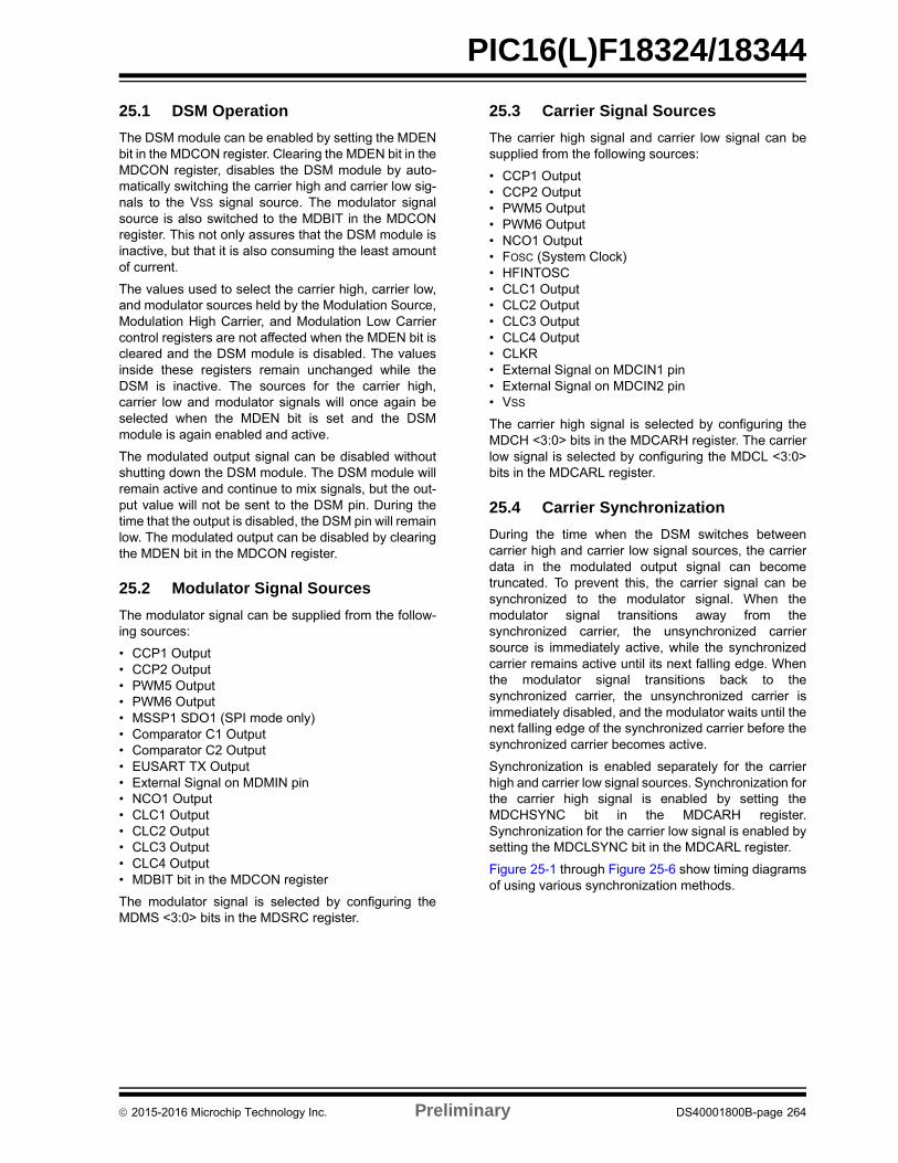
PIC16(L)F18324/18344
25.1 DSM Operation
The DSM module can be enabled by setting the MDENbit in the MDCON register. Clearing the MDEN bit in theMDCON register, disables the DSM module by auto-matically switching the carrier high and carrier low sig-nals to the VSS signal source. The modulator signalsource is also switched to the MDBIT in the MDCONregister. This not only assures that the DSM module isinactive, but that it is also consuming the least amountof current.
The values used to select the carrier high, carrier low,and modulator sources held by the Modulation Source,Modulation High Carrier, and Modulation Low Carriercontrol registers are not affected when the MDEN bit iscleared and the DSM module is disabled. The valuesinside these registers remain unchanged while theDSM is inactive. The sources for the carrier high,carrier low and modulator signals will once again beselected when the MDEN bit is set and the DSMmodule is again enabled and active.
The modulated output signal can be disabled withoutshutting down the DSM module. The DSM module willremain active and continue to mix signals, but the out-put value will not be sent to the DSM pin. During thetime that the output is disabled, the DSM pin will remainlow. The modulated output can be disabled by clearingthe MDEN bit in the MDCON register.
25.2 Modulator Signal Sources
The modulator signal can be supplied from the follow-ing sources:
• CCP1 Output• CCP2 Output• PWM5 Output• PWM6 Output• MSSP1 SDO1 (SPI mode only)• Comparator C1 Output• Comparator C2 Output• EUSART TX Output• External Signal on MDMIN pin• NCO1 Output• CLC1 Output• CLC2 Output• CLC3 Output• CLC4 Output• MDBIT bit in the MDCON register
The modulator signal is selected by configuring theMDMS <3:0> bits in the MDSRC register.
25.3 Carrier Signal Sources
The carrier high signal and carrier low signal can besupplied from the following sources:
• CCP1 Output• CCP2 Output• PWM5 Output• PWM6 Output• NCO1 Output• FOSC (System Clock)• HFINTOSC• CLC1 Output• CLC2 Output• CLC3 Output• CLC4 Output• CLKR• External Signal on MDCIN1 pin • External Signal on MDCIN2 pin• VSS
The carrier high signal is selected by configuring theMDCH <3:0> bits in the MDCARH register. The carrierlow signal is selected by configuring the MDCL <3:0>bits in the MDCARL register.
25.4 Carrier Synchronization
During the time when the DSM switches betweencarrier high and carrier low signal sources, the carrierdata in the modulated output signal can becometruncated. To prevent this, the carrier signal can besynchronized to the modulator signal. When themodulator signal transitions away from thesynchronized carrier, the unsynchronized carriersource is immediately active, while the synchronizedcarrier remains active until its next falling edge. Whenthe modulator signal transitions back to thesynchronized carrier, the unsynchronized carrier isimmediately disabled, and the modulator waits until thenext falling edge of the synchronized carrier before thesynchronized carrier becomes active.
Synchronization is enabled separately for the carrierhigh and carrier low signal sources. Synchronization forthe carrier high signal is enabled by setting theMDCHSYNC bit in the MDCARH register.Synchronization for the carrier low signal is enabled bysetting the MDCLSYNC bit in the MDCARL register.
Figure 25-1 through Figure 25-6 show timing diagramsof using various synchronization methods.
2015-2016 Microchip Technology Inc. Preliminary DS40001800B-page 264
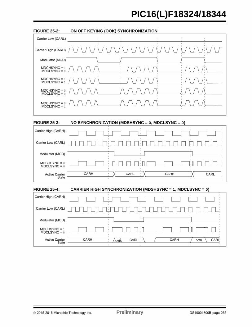
PIC16(L)F18324/18344
FIGURE 25-2: ON OFF KEYING (OOK) SYNCHRONIZATION
FIGURE 25-3: NO SYNCHRONIZATION (MDSHSYNC = 0, MDCLSYNC = 0)
FIGURE 25-4: CARRIER HIGH SYNCHRONIZATION (MDSHSYNC = 1, MDCLSYNC = 0)
Carrier Low (CARL)
MDCHSYNC = 1MDCLSYNC = 0
MDCHSYNC = 1MDCLSYNC = 1
MDCHSYNC = 0MDCLSYNC = 0
MDCHSYNC = 0MDCLSYNC = 1
Carrier High (CARH)
Modulator (MOD)
MDCHSYNC = 0MDCLSYNC = 0
Modulator (MOD)
Carrier High (CARH)
Carrier Low (CARL)
Active Carrier CARH CARL CARLCARHState
MDCHSYNC = 1MDCLSYNC = 0
Modulator (MOD)
Carrier High (CARH)
Carrier Low (CARL)
Active Carrier CARH CARL CARLCARHState both both
2015-2016 Microchip Technology Inc. Preliminary DS40001800B-page 265
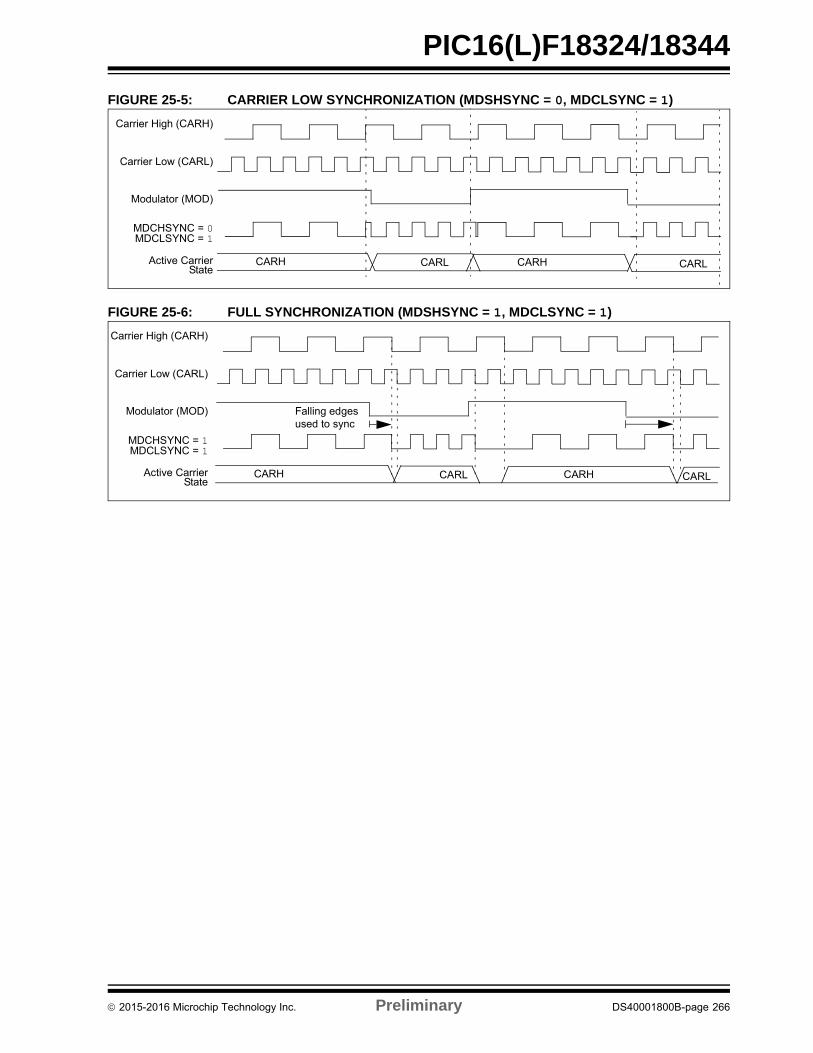
PIC16(L)F18324/18344
FIGURE 25-5: CARRIER LOW SYNCHRONIZATION (MDSHSYNC = 0, MDCLSYNC = 1)
FIGURE 25-6: FULL SYNCHRONIZATION (MDSHSYNC = 1, MDCLSYNC = 1)
MDCHSYNC = 0MDCLSYNC = 1
Modulator (MOD)
Carrier High (CARH)
Carrier Low (CARL)
Active Carrier CARH CARL CARLCARHState
MDCHSYNC = 1MDCLSYNC = 1
Modulator (MOD)
Carrier High (CARH)
Carrier Low (CARL)
Active Carrier CARH CARL CARLCARHState
Falling edgesused to sync
2015-2016 Microchip Technology Inc. Preliminary DS40001800B-page 266
PIC16(L)F18324/18344
25.5 Carrier Source Polarity Select
The signal provided from any selected input source forthe carrier high and carrier low signals can be inverted.Inverting the signal for the carrier high source isenabled by setting the MDCHPOL bit of the MDCARHregister. Inverting the signal for the carrier low source isenabled by setting the MDCLPOL bit of the MDCARLregister.
25.6 Programmable Modulator Data
The MDBIT of the MDCON register can be selected asthe source for the modulator signal. This gives the userthe ability to program the value used for modulation.
25.7 Modulated Output Polarity
The modulated output signal provided on the DSM pincan also be inverted. Inverting the modulated outputsignal is enabled by setting the MDOPOL bit of theMDCON register.
25.8 Slew Rate Control
The slew rate limitation on the output port pin can bedisabled. The slew rate limitation can be removed byclearing the SLR bit of the SLRCON registerassociated with that pin. For example, clearing the slewrate limitation for pin RA5 would require clearing theSLRA5 bit of the SLRCONA register.
25.9 Operation in Sleep Mode
The DSM module is not affected by Sleep mode. TheDSM can still operate during Sleep, if the Carrier andModulator input sources are also still operable duringSleep.
25.10 Effects of a Reset
Upon any device Reset, the DSM module is disabled.The user’s firmware is responsible for initializing themodule before enabling the output. The registers arereset to their default values.
2015-2016 Microchip Technology Inc. Preliminary DS40001800B-page 267
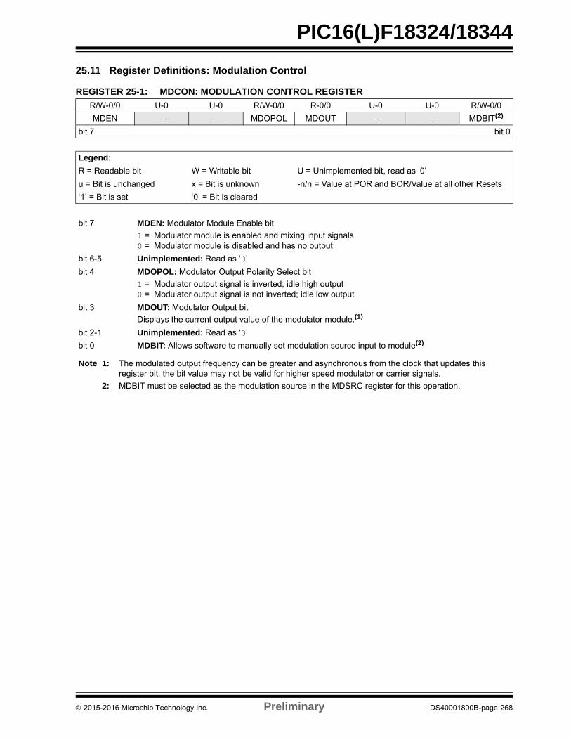
PIC16(L)F18324/18344
25.11 Register Definitions: Modulation Control
REGISTER 25-1: MDCON: MODULATION CONTROL REGISTER
R/W-0/0 U-0 U-0 R/W-0/0 R-0/0 U-0 U-0 R/W-0/0
MDEN — — MDOPOL MDOUT — — MDBIT(2)
bit 7 bit 0
Legend:
R = Readable bit W = Writable bit U = Unimplemented bit, read as ‘0’
u = Bit is unchanged x = Bit is unknown -n/n = Value at POR and BOR/Value at all other Resets
‘1’ = Bit is set ‘0’ = Bit is cleared
bit 7 MDEN: Modulator Module Enable bit
1 = Modulator module is enabled and mixing input signals0 = Modulator module is disabled and has no output
bit 6-5 Unimplemented: Read as ‘0’
bit 4 MDOPOL: Modulator Output Polarity Select bit
1 = Modulator output signal is inverted; idle high output0 = Modulator output signal is not inverted; idle low output
bit 3 MDOUT: Modulator Output bit
Displays the current output value of the modulator module.(1)
bit 2-1 Unimplemented: Read as ‘0’
bit 0 MDBIT: Allows software to manually set modulation source input to module(2)
Note 1: The modulated output frequency can be greater and asynchronous from the clock that updates this register bit, the bit value may not be valid for higher speed modulator or carrier signals.
2: MDBIT must be selected as the modulation source in the MDSRC register for this operation.
2015-2016 Microchip Technology Inc. Preliminary DS40001800B-page 268
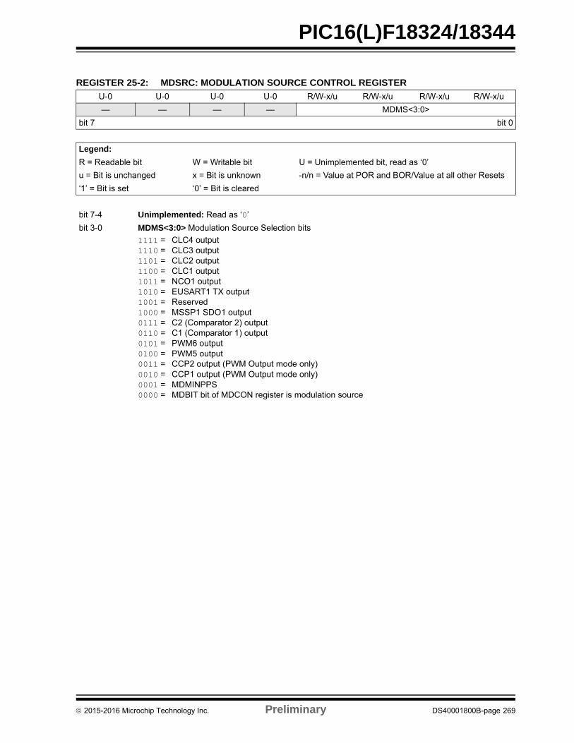
PIC16(L)F18324/18344
REGISTER 25-2: MDSRC: MODULATION SOURCE CONTROL REGISTER
U-0 U-0 U-0 U-0 R/W-x/u R/W-x/u R/W-x/u R/W-x/u
— — — — MDMS<3:0>
bit 7 bit 0
Legend:
R = Readable bit W = Writable bit U = Unimplemented bit, read as ‘0’
u = Bit is unchanged x = Bit is unknown -n/n = Value at POR and BOR/Value at all other Resets
‘1’ = Bit is set ‘0’ = Bit is cleared
bit 7-4 Unimplemented: Read as ‘0’
bit 3-0 MDMS<3:0> Modulation Source Selection bits
1111 = CLC4 output1110 = CLC3 output1101 = CLC2 output1100 = CLC1 output1011 = NCO1 output1010 = EUSART1 TX output1001 = Reserved1000 = MSSP1 SDO1 output0111 = C2 (Comparator 2) output0110 = C1 (Comparator 1) output0101 = PWM6 output0100 = PWM5 output0011 = CCP2 output (PWM Output mode only)0010 = CCP1 output (PWM Output mode only)0001 = MDMINPPS0000 = MDBIT bit of MDCON register is modulation source
2015-2016 Microchip Technology Inc. Preliminary DS40001800B-page 269
PIC16(L)F18324/18344
REGISTER 25-3: MDCARH: MODULATION HIGH CARRIER CONTROL REGISTER
U-0 R/W-x/u R/W-x/u U-0 R/W-x/u R/W-x/u R/W-x/u R/W-x/u
— MDCHPOL MDCHSYNC — MDCH<3:0>(1)
bit 7 bit 0
Legend:
R = Readable bit W = Writable bit U = Unimplemented bit, read as ‘0’
u = Bit is unchanged x = Bit is unknown -n/n = Value at POR and BOR/Value at all other Resets
‘1’ = Bit is set ‘0’ = Bit is cleared
bit 7 Unimplemented: Read as ‘0’
bit 6 MDCHPOL: Modulator High Carrier Polarity Select bit
1 = Selected high carrier signal is inverted0 = Selected high carrier signal is not inverted
bit 5 MDCHSYNC: Modulator High Carrier Synchronization Enable bit
1 = Modulator waits for a falling edge on the high time carrier signal before allowing a switch to thelow time carrier
0 = Modulator Output is not synchronized to the high time carrier signal(1)
bit 4 Unimplemented: Read as ‘0’
bit 3-0 MDCH<3:0> Modulator Data High Carrier Selection bits (1)
1111 = CLC4 output1110 = CLC3 output1101 = CLC2 output1100 = CLC1 output1011 = HFINTOSC1010 = FOSC
1001 = Reserved. No channel connected.1000 = NCO1 output0111 = PWM6 output0110 = PWM5 output0101 = CCP2 output (PWM Output mode only)0100 = CCP1 output (PWM Output mode only)0011 = Reference clock module signal (CLKR)0010 = MDCIN2PPS0001 = MDCIN1PPS0000 = VSS
Note 1: Narrowed carrier pulse widths or spurs may occur in the signal stream if the carrier is not synchronized.
2015-2016 Microchip Technology Inc. Preliminary DS40001800B-page 270

PIC16(L)F18324/18344
REGISTER 25-4: MDCARL: MODULATION LOW CARRIER CONTROL REGISTER
U-0 R/W-x/u R/W-x/u U-0 R/W-x/u R/W-x/u R/W-x/u R/W-x/u
— MDCLPOL MDCLSYNC — MDCL<3:0>(1)
bit 7 bit 0
Legend:
R = Readable bit W = Writable bit U = Unimplemented bit, read as ‘0’
u = Bit is unchanged x = Bit is unknown -n/n = Value at POR and BOR/Value at all other Resets
‘1’ = Bit is set ‘0’ = Bit is cleared
bit 7 Unimplemented: Read as ‘0’
bit 6 MDCLPOL: Modulator Low Carrier Polarity Select bit
1 = Selected low carrier signal is inverted0 = Selected low carrier signal is not inverted
bit 5 MDCLSYNC: Modulator Low Carrier Synchronization Enable bit
1 = Modulator waits for a falling edge on the low time carrier signal before allowing a switch to the hightime carrier
0 = Modulator Output is not synchronized to the low time carrier signal(1)
bit 4 Unimplemented: Read as ‘0’
bit 3-0 MDCL<3:0> Modulator Data High Carrier Selection bits (1)
1111 = CLC4 output1110 = CLC3 output1101 = CLC2 output1100 = CLC1 output1011 = HFINTOSC1010 = FOSC
1001 = Reserved. No channel connected.1000 = NCO1 output0111 = PWM6 output0110 = PWM5 output0101 = CCP2 output (PWM Output mode only)0100 = CCP1 output (PWM Output mode only)0011 = Reference clock module signal (CLKR)0010 = MDCIN2PPS0001 = MDCIN1PPS0000 = VSS
Note 1: Narrowed carrier pulse widths or spurs may occur in the signal stream if the carrier is not synchronized.
2015-2016 Microchip Technology Inc. Preliminary DS40001800B-page 271
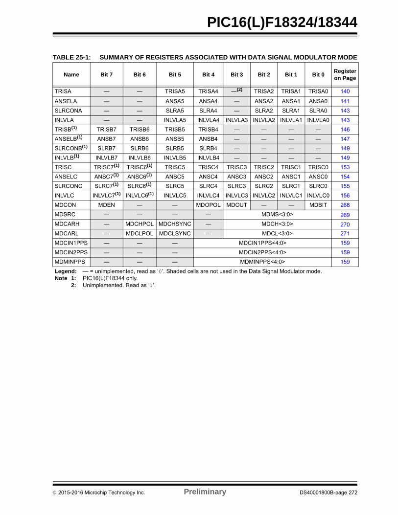
PIC16(L)F18324/18344
TABLE 25-1: SUMMARY OF REGISTERS ASSOCIATED WITH DATA SIGNAL MODULATOR MODE
Name Bit 7 Bit 6 Bit 5 Bit 4 Bit 3 Bit 2 Bit 1 Bit 0Register on Page
TRISA ― ― TRISA5 TRISA4 ―(2) TRISA2 TRISA1 TRISA0 140
ANSELA ― ― ANSA5 ANSA4 ― ANSA2 ANSA1 ANSA0 141
SLRCONA ― ― SLRA5 SLRA4 ― SLRA2 SLRA1 SLRA0 143
INLVLA ― ― INLVLA5 INLVLA4 INLVLA3 INLVLA2 INLVLA1 INLVLA0 143
TRISB(1) TRISB7 TRISB6 TRISB5 TRISB4 ― ― ― ― 146
ANSELB(1) ANSB7 ANSB6 ANSB5 ANSB4 ― ― ― ― 147
SLRCONB(1) SLRB7 SLRB6 SLRB5 SLRB4 ― ― ― ― 149
INLVLB(1) INLVLB7 INLVLB6 INLVLB5 INLVLB4 ― ― ― ― 149
TRISC TRISC7(1) TRISC6(1) TRISC5 TRISC4 TRISC3 TRISC2 TRISC1 TRISC0 153
ANSELC ANSC7(1) ANSC6(1) ANSC5 ANSC4 ANSC3 ANSC2 ANSC1 ANSC0 154
SLRCONC SLRC7(1) SLRC6(1) SLRC5 SLRC4 SLRC3 SLRC2 SLRC1 SLRC0 155
INLVLC INLVLC7(1) INLVLC6(1) INLVLC5 INLVLC4 INLVLC3 INLVLC2 INLVLC1 INLVLC0 156
MDCON MDEN ― ― MDOPOL MDOUT ― ― MDBIT 268
MDSRC ― ― ― ― MDMS<3:0> 269
MDCARH ― MDCHPOL MDCHSYNC ― MDCH<3:0> 270
MDCARL ― MDCLPOL MDCLSYNC ― MDCL<3:0> 271
MDCIN1PPS ― ― ― MDCIN1PPS<4:0> 159
MDCIN2PPS ― ― ― MDCIN2PPS<4:0> 159
MDMINPPS ― ― ― MDMINPPS<4:0> 159
Legend: — = unimplemented, read as ‘0’. Shaded cells are not used in the Data Signal Modulator mode.Note 1: PIC16(L)F18344 only.
2: Unimplemented. Read as ‘1’.
2015-2016 Microchip Technology Inc. Preliminary DS40001800B-page 272
PIC16(L)F18324/18344
26.0 TIMER0 MODULE
The Timer0 module is an 8/16-bit timer/counter with thefollowing features:
• 16-bit timer/counter • 8-bit timer/counter with programmable period• Synchronous or asynchronous operation• Selectable clock sources• Programmable prescaler (independent of
Watchdog Timer)• Programmable postscaler• Operation during Sleep mode• Interrupt on match or overflow• Output on I/O pin (via PPS) or to other peripherals
26.1 Timer0 Operation
Timer0 can operate as either an 8-bit timer/counter ora 16-bit timer/counter. The mode is selected with theT016BIT bit of the T0CON register.
When used with FOSC/4 clock source, the module is atimer and increments on every instruction cycle. Whenused with any other clock source, the module can beused as either a timer or a counter and increments onevery rising edge of the external source.
26.1.1 16-BIT MODE
In normal operation, TMR0 increments on the risingedge of the clock source. A 15-bit prescaler on theclock input gives several prescale options (seeprescaler control bits, T0CKPS<3:0> in the T0CON1register).
26.1.1.1 Timer0 Reads and Writes in 16-Bit Mode
TMR0H is not the actual high byte of Timer0 in 16-bitmode. It is actually a buffered version of the real highbyte of Timer0, which is neither directly readable norwritable (see Figure 26-1). TMR0H is updated with thecontents of the high byte of Timer0 during a read ofTMR0L. This provides the ability to read all 16 bits ofTimer0 without having to verify that the read of the highand low byte was valid, due to a rollover betweensuccessive reads of the high and low byte.
Similarly, a write to the high byte of Timer0 must alsotake place through the TMR0H Buffer register. The highbyte is updated with the contents of TMR0H when awrite occurs to TMR0L. This allows all 16 bits of Timer0to be updated at once.
26.1.2 8-BIT MODE
In normal operation, TMR0 increments on the risingedge of the clock source. A 15-bit prescaler on theclock input gives several prescale options (seeprescaler control bits, T0CKPS<3:0> in the T0CON1register).
In 8-bit mode, TMR0H no longer functions as theTimer0 high byte, but instead functions as the PeriodRegister (PR). The value of TMR0L is compared to thatof TMR0H on each clock cycle. When the two valuesmatch, the following events happen:
• TMR0_out goes high for one prescaled clock period
• TMR0L is reset• The contents of TMR0H are copied to the period
buffer
In 8-bit mode, the TMR0L and TMR0H registers areboth directly readable and writable. The TMR0Lregister is cleared on any device Reset, while theTMR0H register initializes at FFh.
Both the prescaler and postscaler counters are clearedon the following events:
• A write to the TMR0L register• A write to either the T0CON0 or T0CON1 regis-
ters.• Any device Reset – Power-on Reset
(POR),MCLR Reset, Watchdog Timer Reset (WDTR) or Brown-out Reset (BOR)
26.1.3 COUNTER MODE
In Counter mode, the prescaler is normally disabled bysetting the T0CKPS bits of the T0CON1 register to‘0000’. Each rising edge of the clock input (or theoutput of the prescaler if the prescaler is used)increments the counter by ‘1’.
26.1.4 TIMER MODE
In Timer mode, the Timer0 module will increment everyinstruction cycle as long as there is a valid clock signaland the T0CKPS bits of the T0CON1 register(Register 26-4) are set to ‘0000’. When a prescaler isadded, the timer will increment at the rate based on theprescaler value.
26.1.5 ASYNCHRONOUS MODE
When the T0ASYNC bit of the T0CON1 register is set(T0ASYNC = 1), the counter increments with eachrising edge of the input source (or output of theprescaler, if used). Asynchronous mode allows thecounter to continue operation during Sleep modeprovided that the clock also continues to operate duringSleep.
2015-2016 Microchip Technology Inc. Preliminary DS40001800B-page 273
PIC16(L)F18324/18344
26.1.6 SYNCHRONOUS MODE
When the T0ASYNC bit of the T0CON1 register is clear(T0ASYNC = 0), the counter clock is synchronized tothe system oscillator (FOSC/4). When operating inSynchronous mode, the counter clock frequencycannot exceed FOSC/4.
26.2 Clock Source Selection
The T0CS<2:0> bits of the T0CON1 register are usedto select the clock source for Timer0. Register 26-4displays the clock source selections.
26.2.1 INTERNAL CLOCK SOURCE
When the internal clock source is selected, Timer0operates as a timer and will increment on multiples ofthe clock source, as determined by the Timer0prescaler.
26.2.2 EXTERNAL CLOCK SOURCE
When an external clock source is selected, Timer0 canoperate as either a timer or a counter. Timer0 willincrement on multiples of the rising edge of the externalclock source, as determined by the Timer0 prescaler.
26.3 Programmable Prescaler
A software programmable prescaler is available forexclusive use with Timer0. There are 16 prescaleroptions for Timer0 ranging in powers of two from 1:1 to1:32768. The prescaler values are selected using theT0CKPS<3:0> bits of the T0CON1 register.
The prescaler is not directly readable or writable.Clearing the prescaler register can be done by writingto the TMR0L register, the T0CON0 register, or theT0CON1 register.
26.4 Programmable Postscaler
A software programmable postscaler (output divider) isavailable for exclusive use with Timer0. There are 16postscaler options for Timer0 ranging from 1:1 to 1:16.The postscaler values are selected using theT0OUTPS<3:0> bits of the T0CON0 register.
The postscaler is not directly readable or writable.Clearing the postscaler register can be done by writingto the TMR0L register, the T0CON0 register, or theT0CON1 register.
26.5 Operation During Sleep
When operating synchronously, Timer0 will halt. Whenoperating asynchronously, Timer0 will continue toincrement and wake the device from Sleep (if Timer0interrupts are enabled) provided that the input clocksource is active.
2015-2016 Microchip Technology Inc. Preliminary DS40001800B-page 274
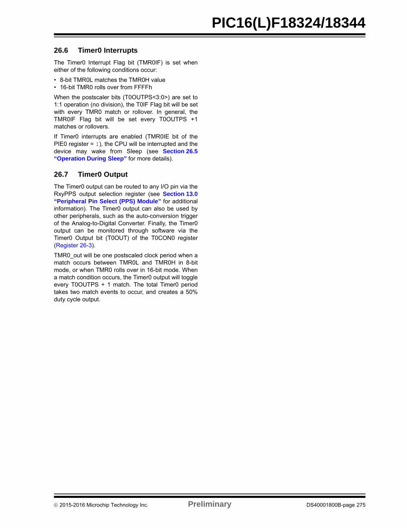
PIC16(L)F18324/18344
26.6 Timer0 Interrupts
The Timer0 Interrupt Flag bit (TMR0IF) is set wheneither of the following conditions occur:
• 8-bit TMR0L matches the TMR0H value• 16-bit TMR0 rolls over from FFFFh
When the postscaler bits (T0OUTPS<3:0>) are set to1:1 operation (no division), the T0IF Flag bit will be setwith every TMR0 match or rollover. In general, theTMR0IF Flag bit will be set every T0OUTPS +1matches or rollovers.
If Timer0 interrupts are enabled (TMR0IE bit of thePIE0 register = 1), the CPU will be interrupted and thedevice may wake from Sleep (see Section 26.5“Operation During Sleep” for more details).
26.7 Timer0 Output
The Timer0 output can be routed to any I/O pin via theRxyPPS output selection register (see Section 13.0“Peripheral Pin Select (PPS) Module” for additionalinformation). The Timer0 output can also be used byother peripherals, such as the auto-conversion triggerof the Analog-to-Digital Converter. Finally, the Timer0output can be monitored through software via theTimer0 Output bit (T0OUT) of the T0CON0 register(Register 26-3).
TMR0_out will be one postscaled clock period when amatch occurs between TMR0L and TMR0H in 8-bitmode, or when TMR0 rolls over in 16-bit mode. Whena match condition occurs, the Timer0 output will toggleevery T0OUTPS + 1 match. The total Timer0 periodtakes two match events to occur, and creates a 50%duty cycle output.
2015-2016 Microchip Technology Inc. Preliminary DS40001800B-page 275
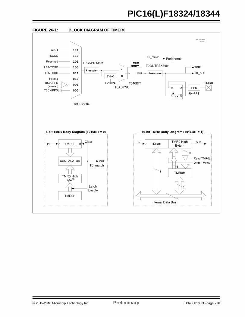
PIC16(L)F18324/18344
FIGURE 26-1: BLOCK DIAGRAM OF TIMER0
Rev. 10-000017B2/27/2014
000
011010001
100101110111
T0CKIPPS
FOSC/4
HFINTOSC
LFINTOSC
Reserved
SOSC
CLC1
T0CKIPPS (Inverted)
T0CS<2:0>
T0CKPS<3:0>
Prescaler
FOSC/4T0ASYNC
T016BIT
T0OUTPS<3:0> T0IF
T0_out
Peripherals
TMR0
10 Postscaler
T0_match
TMR0L
COMPARATOR
TMR0 High Byte(1)
TMR0H
T0_match
Clear
Latch Enable
8-bit TMR0 Body Diagram (T016BIT = 0)
TMR0L
TMR0H
Internal Data Bus
16-bit TMR0 Body Diagram (T016BIT = 1)
SYNCIN OUT
TMR0 BODY
Q
Q
D
CK
PPS
RxyPPS
RIN
OUT
TMR0 High Byte(1)
IN OUT
Read TMR0LWrite TMR0L
8
8
8
8
8
2015-2016 Microchip Technology Inc. Preliminary DS40001800B-page 276
PIC16(L)F18324/18344
26.8 Register Definitions: Timer0 Register
REGISTER 26-1: TMR0L: TIMER0 COUNT REGISTER
R/W-0/0 R/W-0/0 R/W-0/0 R/W-0/0 R/W-0/0 R/W-0/0 R/W-0/0 R/W-0/0
TMR0L<7:0>
bit 7 bit 0
Legend:
R = Readable bit W = Writable bit U = Unimplemented bit, read as ‘0’
u = Bit is unchanged x = Bit is unknown -n/n = Value at POR and BOR/Value at all other Resets
‘1’ = Bit is set ‘0’ = Bit is cleared
bit 7-0 TMR0L<7:0>:TMR0 Counter bits 7..0
REGISTER 26-2: TMR0H: TIMER0 PERIOD REGISTER
R/W-1/1 R/W-1/1 R/W-1/1 R/W-1/1 R/W-1/1 R/W-1/1 R/W-1/1 R/W-1/1
TMR0H<7:0> or TMR0<15:8>
bit 7 bit 0
Legend:
R = Readable bit W = Writable bit U = Unimplemented bit, read as ‘0’
u = Bit is unchanged x = Bit is unknown -n/n = Value at POR and BOR/Value at all other Resets
‘1’ = Bit is set ‘0’ = Bit is cleared
bit 7-0 When T016BIT = 0
TMR0H<7:0>:TMR0 Period Register bits 7..0When T016BIT = 1TMR0<15:8>: TMR0 Counter bits 15..8
2015-2016 Microchip Technology Inc. Preliminary DS40001800B-page 277
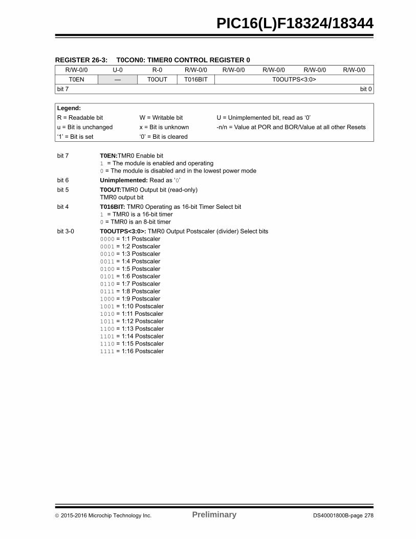
PIC16(L)F18324/18344
REGISTER 26-3: T0CON0: TIMER0 CONTROL REGISTER 0
R/W-0/0 U-0 R-0 R/W-0/0 R/W-0/0 R/W-0/0 R/W-0/0 R/W-0/0
T0EN — T0OUT T016BIT T0OUTPS<3:0>
bit 7 bit 0
Legend:
R = Readable bit W = Writable bit U = Unimplemented bit, read as ‘0’
u = Bit is unchanged x = Bit is unknown -n/n = Value at POR and BOR/Value at all other Resets
‘1’ = Bit is set ‘0’ = Bit is cleared
bit 7 T0EN:TMR0 Enable bit1 = The module is enabled and operating0 = The module is disabled and in the lowest power mode
bit 6 Unimplemented: Read as ‘0’
bit 5 T0OUT:TMR0 Output bit (read-only)TMR0 output bit
bit 4 T016BIT: TMR0 Operating as 16-bit Timer Select bit1 = TMR0 is a 16-bit timer0 = TMR0 is an 8-bit timer
bit 3-0 T0OUTPS<3:0>: TMR0 Output Postscaler (divider) Select bits0000 = 1:1 Postscaler0001 = 1:2 Postscaler0010 = 1:3 Postscaler0011 = 1:4 Postscaler0100 = 1:5 Postscaler0101 = 1:6 Postscaler0110 = 1:7 Postscaler0111 = 1:8 Postscaler1000 = 1:9 Postscaler1001 = 1:10 Postscaler1010 = 1:11 Postscaler1011 = 1:12 Postscaler1100 = 1:13 Postscaler1101 = 1:14 Postscaler1110 = 1:15 Postscaler1111 = 1:16 Postscaler
2015-2016 Microchip Technology Inc. Preliminary DS40001800B-page 278
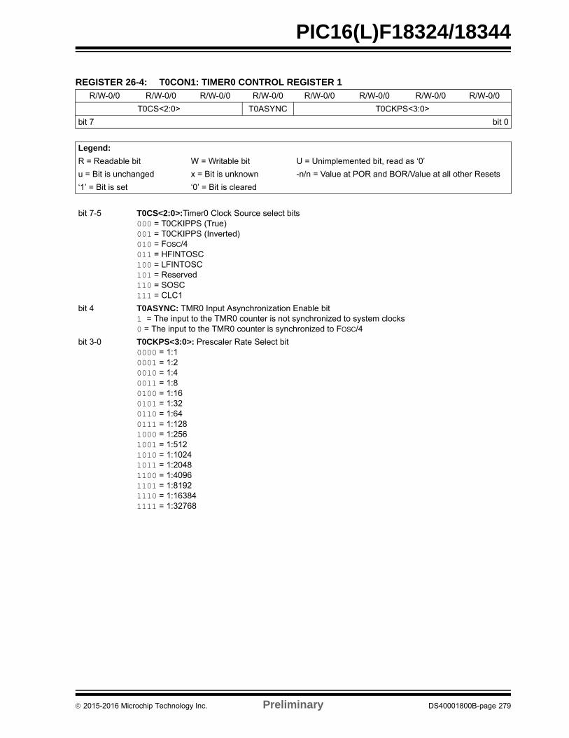
PIC16(L)F18324/18344
REGISTER 26-4: T0CON1: TIMER0 CONTROL REGISTER 1
R/W-0/0 R/W-0/0 R/W-0/0 R/W-0/0 R/W-0/0 R/W-0/0 R/W-0/0 R/W-0/0
T0CS<2:0> T0ASYNC T0CKPS<3:0>
bit 7 bit 0
Legend:
R = Readable bit W = Writable bit U = Unimplemented bit, read as ‘0’
u = Bit is unchanged x = Bit is unknown -n/n = Value at POR and BOR/Value at all other Resets
‘1’ = Bit is set ‘0’ = Bit is cleared
bit 7-5 T0CS<2:0>:Timer0 Clock Source select bits000 = T0CKIPPS (True)001 = T0CKIPPS (Inverted)010 = FOSC/4011 = HFINTOSC100 = LFINTOSC101 = Reserved110 = SOSC111 = CLC1
bit 4 T0ASYNC: TMR0 Input Asynchronization Enable bit1 = The input to the TMR0 counter is not synchronized to system clocks0 = The input to the TMR0 counter is synchronized to FOSC/4
bit 3-0 T0CKPS<3:0>: Prescaler Rate Select bit0000 = 1:1 0001 = 1:2 0010 = 1:4 0011 = 1:8 0100 = 1:16 0101 = 1:32 0110 = 1:64 0111 = 1:128 1000 = 1:256 1001 = 1:512 1010 = 1:1024 1011 = 1:2048 1100 = 1:4096 1101 = 1:8192 1110 = 1:16384 1111 = 1:32768
2015-2016 Microchip Technology Inc. Preliminary DS40001800B-page 279
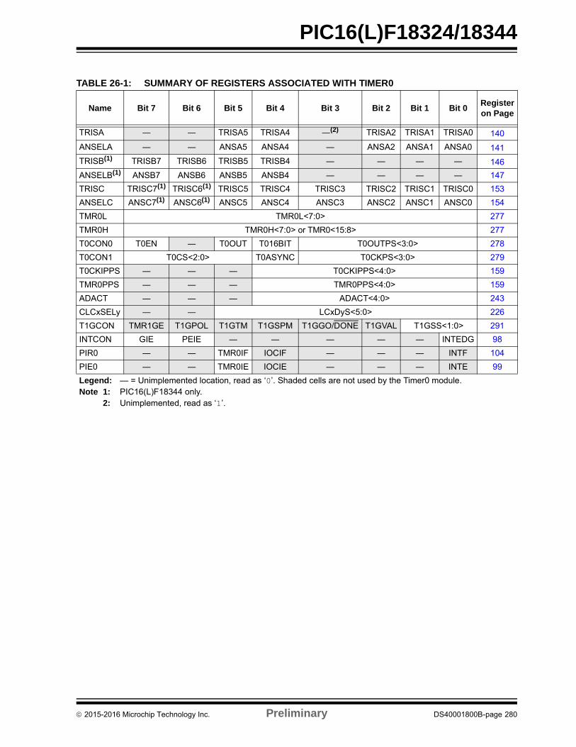
PIC16(L)F18324/18344
TABLE 26-1: SUMMARY OF REGISTERS ASSOCIATED WITH TIMER0
Name Bit 7 Bit 6 Bit 5 Bit 4 Bit 3 Bit 2 Bit 1 Bit 0Register on Page
TRISA ― ― TRISA5 TRISA4 ―(2) TRISA2 TRISA1 TRISA0 140
ANSELA ― ― ANSA5 ANSA4 ― ANSA2 ANSA1 ANSA0 141
TRISB(1) TRISB7 TRISB6 TRISB5 TRISB4 ― ― ― ― 146
ANSELB(1) ANSB7 ANSB6 ANSB5 ANSB4 ― ― ― ― 147
TRISC TRISC7(1) TRISC6(1) TRISC5 TRISC4 TRISC3 TRISC2 TRISC1 TRISC0 153
ANSELC ANSC7(1) ANSC6(1) ANSC5 ANSC4 ANSC3 ANSC2 ANSC1 ANSC0 154
TMR0L TMR0L<7:0> 277
TMR0H TMR0H<7:0> or TMR0<15:8> 277
T0CON0 T0EN ― T0OUT T016BIT T0OUTPS<3:0> 278
T0CON1 T0CS<2:0> T0ASYNC T0CKPS<3:0> 279
T0CKIPPS ― ― ― T0CKIPPS<4:0> 159
TMR0PPS ― ― ― TMR0PPS<4:0> 159
ADACT ― ― ― ADACT<4:0> 243
CLCxSELy ― ― LCxDyS<5:0> 226
T1GCON TMR1GE T1GPOL T1GTM T1GSPM T1GGO/DONE T1GVAL T1GSS<1:0> 291
INTCON GIE PEIE ― ― ― ― ― INTEDG 98
PIR0 ― ― TMR0IF IOCIF ― ― ― INTF 104
PIE0 ― ― TMR0IE IOCIE ― ― ― INTE 99
Legend: — = Unimplemented location, read as ‘0’. Shaded cells are not used by the Timer0 module.Note 1: PIC16(L)F18344 only.
2: Unimplemented, read as ‘1’.
2015-2016 Microchip Technology Inc. Preliminary DS40001800B-page 280
PIC16(L)F18324/18344
27.0 TIMER1/3/5 MODULE WITH GATE CONTROL
Timer1/3/5 modules are 16-bit timers/counters, eachwith the following features:
• 16-bit timer/counter register pair (TMR1H:TMR1L)• Programmable internal or external clock source• 2-bit prescaler• Clock source for optional comparator
synchronization• Multiple Timer1 gate (count enable) sources• Interrupt on overflow• Wake-up on overflow (external clock,
Asynchronous mode only)• Time base for the Capture/Compare function with
the CCP modules• Auto-conversion Trigger (with CCP)• Selectable Gate Source Polarity• Gate Toggle mode• Gate Single-pulse mode• Gate Value Status• Gate Event Interrupt
Figure 27-1 is a block diagram of the Timer1 module.
Note 1: In devices with more than one Timermodule, it is very important to pay closeattention to the register names used. Anumber placed after the module acronymis used to distinguish between separatemodules. For example, the T1CON andT3CON control the same operationalaspects of two completely different Timermodules.
2: Throughout this section, genericreferences to Timer1 module in any of itsoperating modes may be interpreted asbeing equally applicable to Timerxmodule. Register names, modulesignals, I/O pins and bit names may usethe generic designator ‘x’ to indicate theuse of a numeral to distinguish aparticular module, when required.
2015-2016 Microchip Technology Inc. Preliminary DS40001800B-page 281
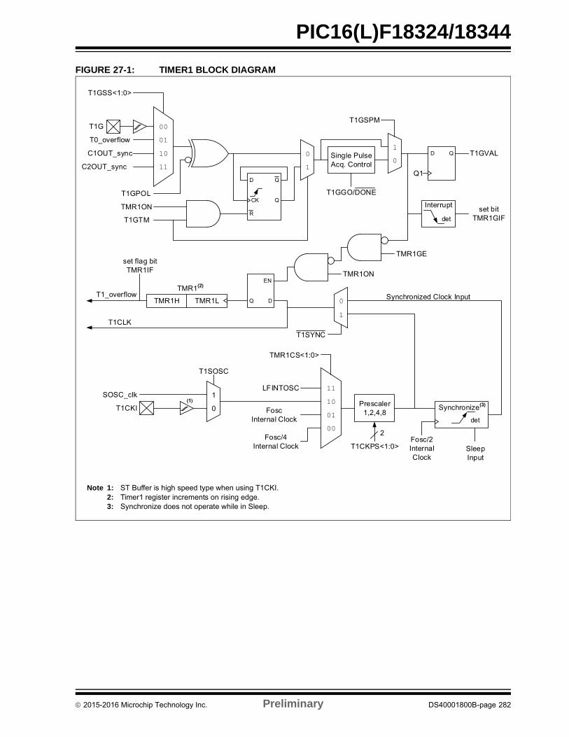
PIC16(L)F18324/18344
FIGURE 27-1: TIMER1 BLOCK DIAGRAM
Note 1: ST Buffer is high speed type when using T1CKI.2: Timer1 register increments on rising edge.3: Synchronize does not operate while in Sleep.
Note 1: ST Buffer is high speed type when using T1CKI.2: Timer1 register increments on rising edge.3: Synchronize does not operate while in Sleep
00
111001
T1G
T0_overflow
C1OUT_sync
C2OUT_sync
T1GSS<1:0>
T1GPOL
01
Single PulseAcq. Control
10
T1GSPM
TMR1ON
T1GTM
TMR1GE
TMR1ON
DQ
EN
TMR1LTMR1HT1_overflow
set flag bitTMR1IF
TMR1(2)
10
FoscInternal Clock
Fosc/4Internal Clock
LFINTOSC
TMR1CS<1:0>
00
111001
Prescaler1,2,4,8
T1SYNC
SleepInput
Fosc/2InternalClock
T1CKPS<1:0>
Synchronized Clock Input
2
det
Synchronize(3)(1)
D
QCK
R
Q
T1GGO/DONE
T1CLK
T1CKI
D Q
set bitTMR1GIF
T1GVAL
Q1
det
Interrupt
SOSC_clk 1
0
T1SOSC
2015-2016 Microchip Technology Inc. Preliminary DS40001800B-page 282

PIC16(L)F18324/18344
27.1 Timer1 Operation
The Timer1 module is a 16-bit incrementing timer whichis accessed through the TMR1H:TMR1L register pair.Writes to TMR1H or TMR1L directly update the timer.
The module can be used with either internal or externalclock sources, and has the Timer1 Gate Enablefunction. When Timer1 is used with the Timer1 GateEnable, the timer can measure time intervals or countsignal pulses between two points of interest. Whenused without the Timer1 Gate Enable, the timer simplymeasures time intervals.
Timer1 is enabled by configuring the TMR1ON andTMR1GE bits in the T1CON and T1GCON registers,respectively. Table 27-1 displays the Timer1 enableselections.
27.2 Clock Source Selection
The TMR1CS<1:0> and T1OSC bits of the T1CONregister are used to select the clock source for Timer1.Table 27-2 displays the clock source selections. TheTMR1H:TMR1L register pair will increment onmultiples of the clock source as determined by theTimer1 prescaler.
When either the FOSC or LFINTOSC clock source isselected, the TMR1H:TMR1L register pair willincrement every rising clock edge. Reading from theTMR1H:TMR1L register pair when either the FOSC orLFINTOSC is the clock source will cause a 2 LSb lossin resolution, which can be mitigated by using anasynchronous input signal to gate the Timer1 clockinput (see Section 26.5 “Operation During Sleep” formore information on the Timer1 Gate Enable).
When the FOSC/4 clock source is selected, theTMR1H:TMR1L register pair increments everyinstruction cycle (once every four FOSC pulses).
In addition to the internal clock sources, Timer1 has adedicated external clock input pin, T1CKI. T1CKI canbe either synchronized to the system clock or can runasynchronously via the T1SYNC bit of the T1CONregister. When the T1CKI pin is used as the clocksource, the TMR1H:TMR1L register pair increments onthe rising edge of the T1CKI clock input.
TABLE 27-1: TIMER1 ENABLE SELECTIONS
TMR1ON TMR1GETimer1
Operation
0 0 Off
0 1 Off
1 0 Always On
1 1 Count Enabled
Note: When using Timer1 to count events, afalling edge must be registered by thecounter prior to the first incrementingrising edge after any one or more of thefollowing conditions:
• Timer1 enabled after POR• Write to TMR1H or TMR1L• Timer1 is disabled• Timer1 is disabled (TMR1ON = 0) when T1CKI is
high then Timer1 is enabled (TMR1ON=1) when T1CKI is low.
TABLE 27-2: CLOCK SOURCE SELECTIONS
TMR1CS<1:0> Clock Source
11 LFINTOSC
10 External Clocking on T1CKI Pin
01 System Clock (FOSC)
00 Instruction Clock (FOSC/4)
2015-2016 Microchip Technology Inc. Preliminary DS40001800B-page 283
PIC16(L)F18324/18344
27.2.1 TIMER1 (SECONDARY) OSCILLATOR
A dedicated low-power 32.768 kHz oscillator circuit isbuilt-in between pins SOSCI (input) and SOSCO(amplifier output). This internal circuit is designed to beused in conjunction with an external 32.768 kHzcrystal.
The oscillator circuit is enabled by setting the T1SOSCbit of the T1CON register. The oscillator will continue torun during Sleep.
27.3 Timer1 Prescaler
Timer1 has four prescaler options allowing 1, 2, 4 or 8divisions of the clock input. The T1CKPS bits of theT1CON register control the prescale counter. Theprescale counter is not directly readable or writable;however, the prescaler counter is cleared upon a write toTMR1H or TMR1L.
27.4 Timer1 Operation in Asynchronous Mode
If the control bit T1SYNC of the T1CON register is set,the external clock input is not synchronized. The timerincrements asynchronously to the internal phaseclocks. If the external clock source is selected then thetimer will continue to run during Sleep and cangenerate an interrupt on overflow, which will wake-upthe processor. However, special precautions insoftware are needed to read/write the timer (seeSection 27.4.1 “Reading and Writing Timer1 inAsynchronous Mode”).
27.4.1 READING AND WRITING TIMER1 IN ASYNCHRONOUS MODE
Reading TMR1H or TMR1L while the timer is runningfrom an external asynchronous clock will ensure a validread (taken care of in hardware). However, the usershould keep in mind that reading the 16-bit timer in two8-bit values itself, poses certain problems, since thetimer may overflow between the reads.
For writes, it is recommended that the user simply stopthe timer and write the desired values. A writecontention may occur by writing to the timer registers,while the register is incrementing. This may produce anunpredictable value in the TMR1H:TMR1L register pair.
27.5 Timer1 Gate
Timer1 can be configured to count freely or the countcan be enabled and disabled using Timer1 gatecircuitry. This is also referred to as Timer1 Gate Enable.
Timer1 gate can also be driven by multiple selectablesources.
27.5.1 TIMER1 GATE ENABLE
The Timer1 Gate Enable mode is enabled by settingthe TMR1GE bit of the T1GCON register. The polarityof the Timer1 Gate Enable mode is configured usingthe T1GPOL bit of the T1GCON register.
When Timer1 Gate Enable mode is enabled, Timer1will increment on the rising edge of the Timer1 clocksource. When Timer1 Gate Enable mode is disabled,no incrementing will occur and Timer1 will hold thecurrent count. See Figure 27-3 for timing details.
Note: The oscillator requires a start-up andstabilization time before use. Thus,T1SOSC should be set and a suitabledelay observed prior to using Timer1. Asuitable delay similar to the OST delaycan be implemented in software byclearing the TMR1IF bit then presettingthe TMR1H:TMR1L register pair toFC00h. The TMR1IF flag will be set when1024 clock cycles have elapsed, therebyindicating that the oscillator is running andreasonably stable.
Note: When switching from synchronous toasynchronous operation, it is possible toskip an increment. When switching fromasynchronous to synchronous operation,it is possible to produce an additionalincrement.
TABLE 27-3: TIMER1 GATE ENABLE SELECTIONS
T1CLK T1GPOL T1G Timer1 Operation
0 0 Counts
0 1 Holds Count
1 0 Holds Count
1 1 Counts
2015-2016 Microchip Technology Inc. Preliminary DS40001800B-page 284
PIC16(L)F18324/18344
27.5.2 TIMER1 GATE SOURCE SELECTION
Timer1 gate source selections are shown in Table 27-4.Source selection is controlled by the T1GSS bits of theT1GCON register. The polarity of the selected input isconfigurable. Polarity selection is controlled by theT1GPOL bit of the T1GCON register.
27.5.2.1 T1G Pin Gate Operation
The T1G pin is one source for Timer1 gate control. Itcan be used to supply an external source to the Timer1gate circuitry.
27.5.2.2 Timer0 Overflow Gate Operation
When Timer0 increments from FFh to 00h, alow-to-high pulse will automatically be generated andinternally supplied to the Timer1 gate circuitry.
27.5.2.3 Comparator C1 Gate Operation
The output resulting from a Comparator 1 operation canbe selected as a source for Timer1 gate control. TheComparator 1 output can be synchronized to the Timer1clock or left asynchronous. For more information seeSection 18.4.1 “Comparator OutputSynchronization”.
27.5.2.4 Comparator C2 Gate Operation
The output resulting from a Comparator 2 operationcan be selected as a source for Timer1 gate control.The Comparator 2 output can be synchronized to theTimer1 clock or left asynchronous. For moreinformation see Section 18.4.1 “Comparator OutputSynchronization”.
27.5.3 TIMER1 GATE TOGGLE MODE
When Timer1 Gate Toggle mode is enabled, it ispossible to measure the full period of a Timer1 gatesignal, as opposed to the duration of a single pulse.
The Timer1 gate source is routed through a flip-flop thatchanges state on every incrementing edge of thesignal. See Figure 27-4 for timing details.
Timer1 Gate Toggle mode is enabled by setting theT1GTM bit of the T1GCON register. When the T1GTMbit is cleared, the flip-flop is cleared and held clear. Thisis necessary in order to control which edge ismeasured.
27.5.4 TIMER1 GATE SINGLE-PULSE MODE
When Timer1 Gate Single-Pulse mode is enabled, it ispossible to capture a single-pulse gate event. Timer1Gate Single-Pulse mode is first enabled by setting theT1GSPM bit in the T1GCON register. Next, theT1GGO/DONE bit in the T1GCON register must be set.The Timer1 will be fully enabled on the nextincrementing edge of the Timer1 gate signal. On thenext trailing edge of the Timer1 gate signal theT1GGO/DONE bit will automatically be cleared. Noother gate events will be allowed to increment Timer1until the T1GGO/DONE bit is once again set insoftware. See Figure 27-5 for timing details.
If the Single-Pulse Gate mode is disabled by clearing theT1GSPM bit in the T1GCON register, the T1GGO/DONEbit should also be cleared.
Enabling the Toggle mode and the Single-Pulse modesimultaneously will permit both sections to worktogether. This allows the period of the Timer1 gatesource to be measured. See Figure 27-6 for timingdetails.
27.5.5 TIMER1 GATE VALUE STATUS
When Timer1 Gate Value Status is utilized, it is possibleto read the most current level of the gate control value.The value is stored in the T1GVAL bit in the T1GCONregister. The T1GVAL bit is valid even when the Timer1gate is not enabled (TMR1GE bit is cleared).
TABLE 27-4: TIMER1 GATE SOURCES
T1GSS Timer1 Gate Source
00 Timer1 Gate Pin
01 Overflow of Timer0(TMR0 increments from FFh to 00h)
10 Comparator 1 Output(optionally Timer1 synchronized output)
11 Comparator 2 Output(optionally Timer1 synchronized output)
Note: Enabling Toggle mode at the same timeas changing the gate polarity may result inindeterminate operation.
2015-2016 Microchip Technology Inc. Preliminary DS40001800B-page 285
PIC16(L)F18324/18344
27.6 Timer1 Interrupt
The Timer1 register pair (TMR1H:TMR1L) incrementsto FFFFh and rolls over to 0000h. When Timer1 rollsover, the Timer1 interrupt flag bit of the PIR1 register isset. To enable the interrupt on rollover, you must setthese bits:
• TMR1ON bit of the T1CON register• TMR1IE bit of the PIE1 register• PEIE bit of the INTCON register• GIE bit of the INTCON register
The interrupt is cleared by clearing the TMR1IF bit inthe Interrupt Service Routine.
27.6.1 TIMER1 GATE EVENT INTERRUPT
When Timer1 Gate Event Interrupt is enabled, it ispossible to generate an interrupt upon the completionof a gate event. When the falling edge of T1GVALoccurs, the TMR1GIF flag bit in the PIR1 register will beset. If the TMR1GIE bit in the PIE1 register is set, thenan interrupt will be recognized.
The TMR1GIF flag bit operates even when the Timer1gate is not enabled (TMR1GE bit is cleared).
27.7 Timer1 Operation During Sleep
Timer1 can only operate during Sleep when setup inAsynchronous mode. In this mode, an external crystalor clock source can be used to increment the counter.To set up the timer to wake the device:
• TMR1ON bit of the T1CON register must be set• TMR1IE bit of the PIE1 register must be set• PEIE bit of the INTCON register must be set• T1SYNC bit of the T1CON register must be set• TMR1CS bits of the T1CON register must be con-
figured• T1SOSC bit of the T1CON register must be con-
figured
The device will wake-up on an overflow and executethe next instructions. If the GIE bit of the INTCONregister is set, the device will call the Interrupt ServiceRoutine.
Secondary oscillator will continue to operate in Sleepregardless of the T1SYNC bit setting.
27.8 CCP Capture/Compare Time Base
The CCP modules use the TMR1H:TMR1L registerpair as the time base when operating in Capture orCompare mode.
In Capture mode, the value in the TMR1H:TMR1Lregister pair is copied into the CCPR1H:CCPR1Lregister pair on a configured event.
In Compare mode, an event is triggered when the valueCCPR1H:CCPR1L register pair matches the value inthe TMR1H:TMR1L register pair. This event can be anAuto-conversion Trigger.
For more information, see Section 29.0“Capture/Compare/PWM Modules”.
27.9 CCP Auto-Conversion Trigger
When any of the CCP’s are configured to trigger anauto-conversion, the trigger will clear theTMR1H:TMR1L register pair. This auto-conversiondoes not cause a Timer1 interrupt. The CCP modulemay still be configured to generate a CCP interrupt.
In this mode of operation, the CCPR1H:CCPR1Lregister pair becomes the period register for Timer1.
Timer1 should be synchronized and FOSC/4 should beselected as the clock source in order to utilize theAuto-conversion Trigger. Asynchronous operation ofTimer1 can cause an Auto-conversion Trigger to bemissed.
In the event that a write to TMR1H or TMR1L coincideswith an Auto-conversion Trigger from the CCP, thewrite will take precedence.
For more information, see Section 29.3.3“Auto-Conversion Trigger”.
Note: The TMR1H:TMR1L register pair and theTMR1IF bit should be cleared beforeenabling interrupts.
2015-2016 Microchip Technology Inc. Preliminary DS40001800B-page 286
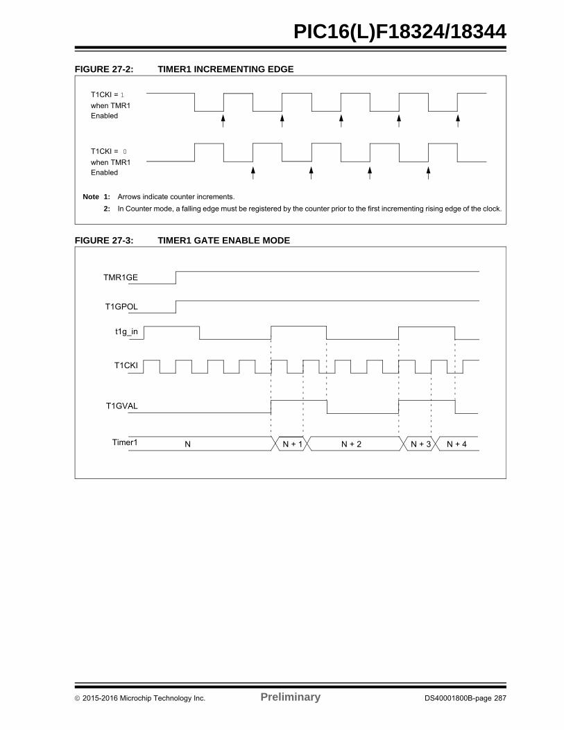
PIC16(L)F18324/18344
FIGURE 27-2: TIMER1 INCREMENTING EDGE
FIGURE 27-3: TIMER1 GATE ENABLE MODE
T1CKI = 1
when TMR1Enabled
T1CKI = 0
when TMR1Enabled
Note 1: Arrows indicate counter increments.
2: In Counter mode, a falling edge must be registered by the counter prior to the first incrementing rising edge of the clock.
TMR1GE
T1GPOL
t1g_in
T1CKI
T1GVAL
Timer1 N N + 1 N + 2 N + 3 N + 4
2015-2016 Microchip Technology Inc. Preliminary DS40001800B-page 287
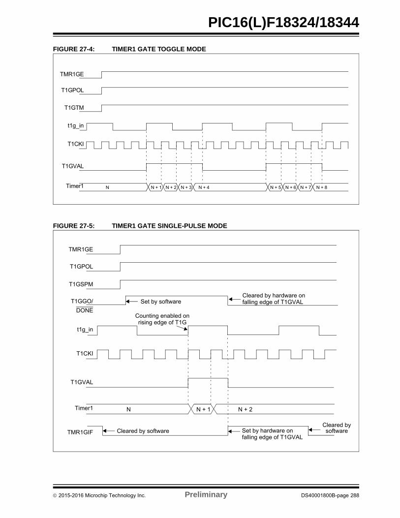
PIC16(L)F18324/18344
FIGURE 27-4: TIMER1 GATE TOGGLE MODE
FIGURE 27-5: TIMER1 GATE SINGLE-PULSE MODE
TMR1GE
T1GPOL
T1GTM
t1g_in
T1CKI
T1GVAL
Timer1 N N + 1 N + 2 N + 3 N + 4 N + 5 N + 6 N + 7 N + 8
TMR1GE
T1GPOL
t1g_in
T1CKI
T1GVAL
Timer1 N N + 1 N + 2
T1GSPM
T1GGO/
DONE
Set by softwareCleared by hardware onfalling edge of T1GVAL
Set by hardware onfalling edge of T1GVAL
Cleared by softwareCleared bysoftwareTMR1GIF
Counting enabled onrising edge of T1G
2015-2016 Microchip Technology Inc. Preliminary DS40001800B-page 288
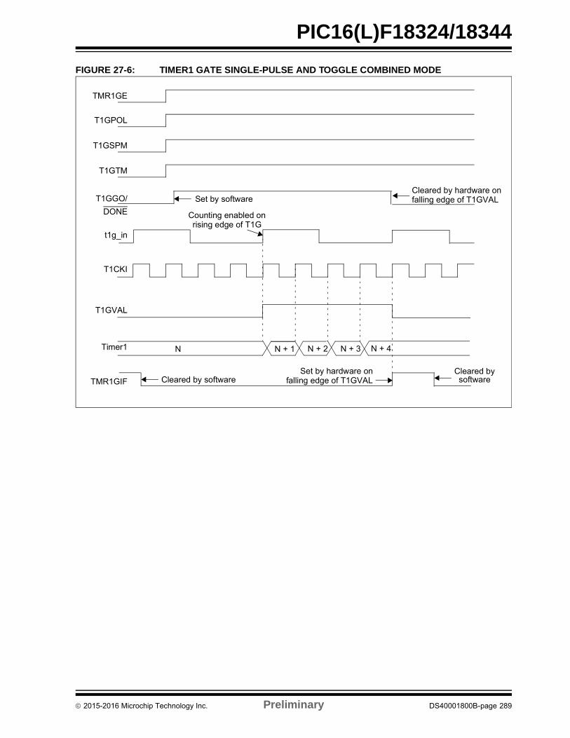
PIC16(L)F18324/18344
FIGURE 27-6: TIMER1 GATE SINGLE-PULSE AND TOGGLE COMBINED MODE
TMR1GE
T1GPOL
t1g_in
T1CKI
T1GVAL
Timer1 N N + 1 N + 2
T1GSPM
T1GGO/
DONE
Set by softwareCleared by hardware onfalling edge of T1GVAL
Set by hardware onfalling edge of T1GVALCleared by software
Cleared bysoftwareTMR1GIF
T1GTM
Counting enabled onrising edge of T1G
N + 4N + 3
2015-2016 Microchip Technology Inc. Preliminary DS40001800B-page 289
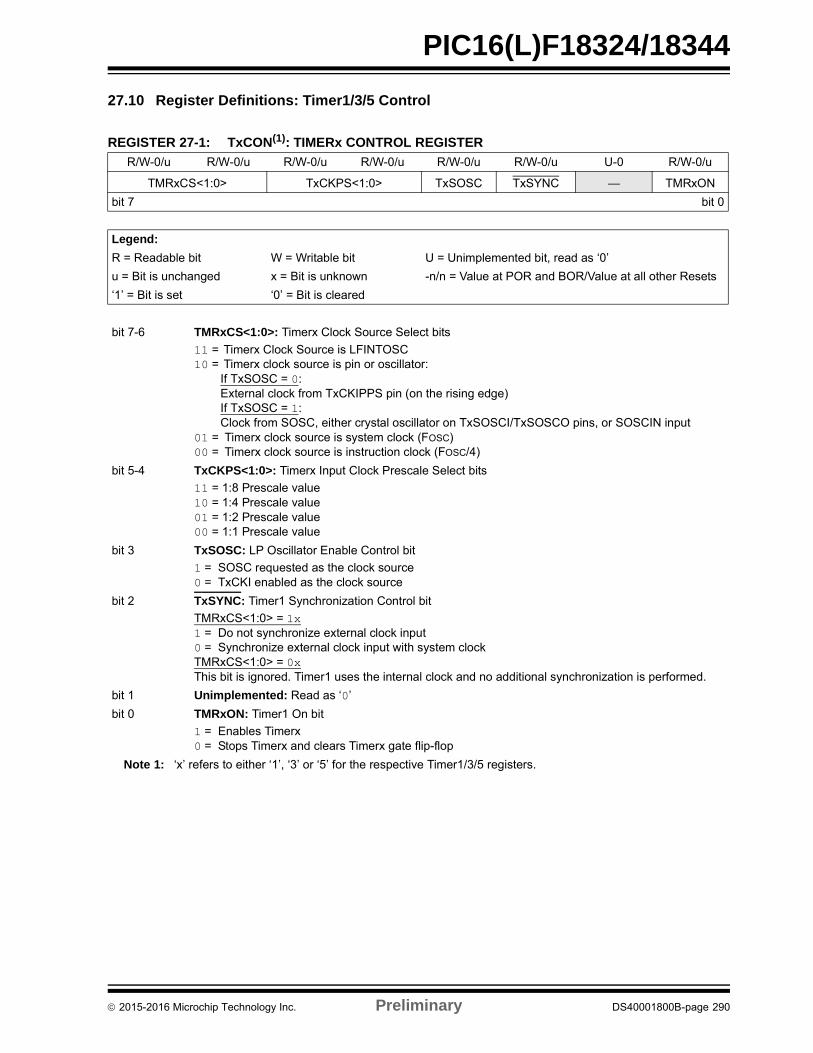
PIC16(L)F18324/18344
27.10 Register Definitions: Timer1/3/5 Control
REGISTER 27-1: TxCON(1): TIMERx CONTROL REGISTER
R/W-0/u R/W-0/u R/W-0/u R/W-0/u R/W-0/u R/W-0/u U-0 R/W-0/u
TMRxCS<1:0> TxCKPS<1:0> TxSOSC TxSYNC — TMRxON
bit 7 bit 0
Legend:
R = Readable bit W = Writable bit U = Unimplemented bit, read as ‘0’
u = Bit is unchanged x = Bit is unknown -n/n = Value at POR and BOR/Value at all other Resets
‘1’ = Bit is set ‘0’ = Bit is cleared
bit 7-6 TMRxCS<1:0>: Timerx Clock Source Select bits
11 = Timerx Clock Source is LFINTOSC10 = Timerx clock source is pin or oscillator:
If TxSOSC = 0:External clock from TxCKIPPS pin (on the rising edge)If TxSOSC = 1:Clock from SOSC, either crystal oscillator on TxSOSCI/TxSOSCO pins, or SOSCIN input
01 = Timerx clock source is system clock (FOSC)00 = Timerx clock source is instruction clock (FOSC/4)
bit 5-4 TxCKPS<1:0>: Timerx Input Clock Prescale Select bits
11 = 1:8 Prescale value10 = 1:4 Prescale value01 = 1:2 Prescale value00 = 1:1 Prescale value
bit 3 TxSOSC: LP Oscillator Enable Control bit
1 = SOSC requested as the clock source0 = TxCKI enabled as the clock source
bit 2 TxSYNC: Timer1 Synchronization Control bit
TMRxCS<1:0> = 1x1 = Do not synchronize external clock input0 = Synchronize external clock input with system clockTMRxCS<1:0> = 0xThis bit is ignored. Timer1 uses the internal clock and no additional synchronization is performed.
bit 1 Unimplemented: Read as ‘0’
bit 0 TMRxON: Timer1 On bit
1 = Enables Timerx0 = Stops Timerx and clears Timerx gate flip-flop
Note 1: ‘x’ refers to either ‘1’, ‘3’ or ‘5’ for the respective Timer1/3/5 registers.
2015-2016 Microchip Technology Inc. Preliminary DS40001800B-page 290

PIC16(L)F18324/18344
REGISTER 27-2: TxGCON(1): TIMERx GATE CONTROL REGISTER
R/W-0/u R/W-0/u R/W-0/u R/W-0/u R/W/HC-0/u R-x/x R/W-0/u R/W-0/u
TMRxGE TxGPOL TxGTM TxGSPM TxGGO/DONE TxGVAL TxGSS<1:0>
bit 7 bit 0
Legend:
R = Readable bit W = Writable bit U = Unimplemented bit, read as ‘0’
u = Bit is unchanged x = Bit is unknown -n/n = Value at POR and BOR/Value at all other Resets
‘1’ = Bit is set ‘0’ = Bit is cleared HC = Bit is cleared by hardware
bit 7 TMRxGE: Timer1 Gate Enable bit
If TMRxON = 0:This bit is ignoredIf TMRxON = 1:1 = Timerx counting is controlled by the Timer1 gate function0 = Timerx is always counting
bit 6 TxGPOL: Timerx Gate Polarity bit
1 = Timerx gate is active-high (Timerx counts when gate is high)0 = Timerx gate is active-low (Timerx counts when gate is low)
bit 5 TxGTM: Timerx Gate Toggle Mode bit
1 = Timerx Gate Toggle mode is enabled0 = Timerx Gate Toggle mode is disabled and toggle flip-flop is clearedTimerx gate flip-flop toggles on every rising edge.
bit 4 TxGSPM: Timerx Gate Single-Pulse Mode bit
1 = Timerx Gate Single-Pulse mode is enabled and is controlling Timerx gate0 = Timerx Gate Single-Pulse mode is disabled
bit 3 TxGGO/DONE: Timerx Gate Single-Pulse Acquisition Status bit
1 = Timerx gate single-pulse acquisition is ready, waiting for an edge0 = Timerx gate single-pulse acquisition has completed or has not been started
This bit is automatically cleared when TxGSPM is cleared
bit 2 TxGVAL: Timerx Gate Value Status bit
Indicates the current state of the Timerx gate, latched at Q1, provided to TMRxH:TMRxLUnaffected by Timerx Gate Enable (TMRxGE)
bit 1-0 TxGSS<1:0>: Timerx Gate Source Select bits
11 = Comparator 2 optionally synchronized output10 = Comparator 1 optionally synchronized output01 = Timer0 overflow output00 = Timerx gate pin
Note 1: ‘x’ refers to either ‘1’, ‘3’ or ‘5’ for the respective Timer1/3/5 registers.
2015-2016 Microchip Technology Inc. Preliminary DS40001800B-page 291
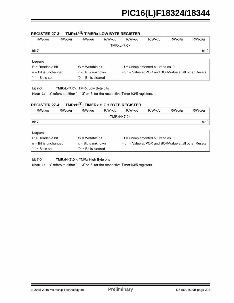
PIC16(L)F18324/18344
REGISTER 27-3: TMRxL(1): TIMERx LOW BYTE REGISTER
R/W-x/u R/W-x/u R/W-x/u R/W-x/u R/W-x/u R/W-x/u R/W-x/u R/W-x/u
TMRxL<7:0>
bit 7 bit 0
Legend:
R = Readable bit W = Writable bit U = Unimplemented bit, read as ‘0’
u = Bit is unchanged x = Bit is unknown -n/n = Value at POR and BOR/Value at all other Resets
‘1’ = Bit is set ‘0’ = Bit is cleared
bit 7-0 TMRxL<7:0>: TMRx Low Byte bits
Note 1: ‘x’ refers to either ‘1’, ‘3’ or ‘5’ for the respective Timer1/3/5 registers.
REGISTER 27-4: TMRxH(1): TIMERx HIGH BYTE REGISTER
R/W-x/u R/W-x/u R/W-x/u R/W-x/u R/W-x/u R/W-x/u R/W-x/u R/W-x/u
TMRxH<7:0>
bit 7 bit 0
Legend:
R = Readable bit W = Writable bit U = Unimplemented bit, read as ‘0’
u = Bit is unchanged x = Bit is unknown -n/n = Value at POR and BOR/Value at all other Resets
‘1’ = Bit is set ‘0’ = Bit is cleared
bit 7-0 TMRxH<7:0>: TMRx High Byte bits
Note 1: ‘x’ refers to either ‘1’, ‘3’ or ‘5’ for the respective Timer1/3/5 registers.
2015-2016 Microchip Technology Inc. Preliminary DS40001800B-page 292
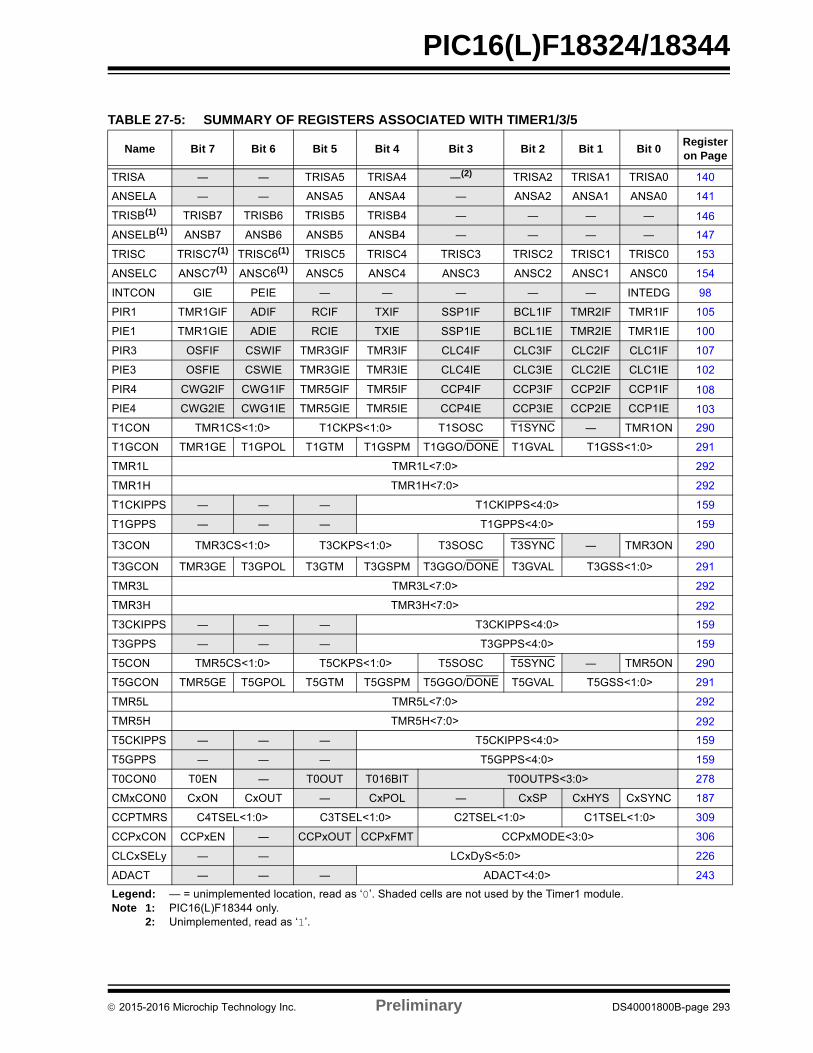
PIC16(L)F18324/18344
TABLE 27-5: SUMMARY OF REGISTERS ASSOCIATED WITH TIMER1/3/5
Name Bit 7 Bit 6 Bit 5 Bit 4 Bit 3 Bit 2 Bit 1 Bit 0Register on Page
TRISA ― ― TRISA5 TRISA4 ―(2) TRISA2 TRISA1 TRISA0 140
ANSELA ― ― ANSA5 ANSA4 ― ANSA2 ANSA1 ANSA0 141
TRISB(1) TRISB7 TRISB6 TRISB5 TRISB4 ― ― ― ― 146
ANSELB(1) ANSB7 ANSB6 ANSB5 ANSB4 ― ― ― ― 147
TRISC TRISC7(1) TRISC6(1) TRISC5 TRISC4 TRISC3 TRISC2 TRISC1 TRISC0 153
ANSELC ANSC7(1) ANSC6(1) ANSC5 ANSC4 ANSC3 ANSC2 ANSC1 ANSC0 154
INTCON GIE PEIE ― ― ― ― ― INTEDG 98
PIR1 TMR1GIF ADIF RCIF TXIF SSP1IF BCL1IF TMR2IF TMR1IF 105
PIE1 TMR1GIE ADIE RCIE TXIE SSP1IE BCL1IE TMR2IE TMR1IE 100
PIR3 OSFIF CSWIF TMR3GIF TMR3IF CLC4IF CLC3IF CLC2IF CLC1IF 107
PIE3 OSFIE CSWIE TMR3GIE TMR3IE CLC4IE CLC3IE CLC2IE CLC1IE 102
PIR4 CWG2IF CWG1IF TMR5GIF TMR5IF CCP4IF CCP3IF CCP2IF CCP1IF 108
PIE4 CWG2IE CWG1IE TMR5GIE TMR5IE CCP4IE CCP3IE CCP2IE CCP1IE 103
T1CON TMR1CS<1:0> T1CKPS<1:0> T1SOSC T1SYNC ― TMR1ON 290
T1GCON TMR1GE T1GPOL T1GTM T1GSPM T1GGO/DONE T1GVAL T1GSS<1:0> 291
TMR1L TMR1L<7:0> 292
TMR1H TMR1H<7:0> 292
T1CKIPPS ― ― ― T1CKIPPS<4:0> 159
T1GPPS ― ― ― T1GPPS<4:0> 159
T3CON TMR3CS<1:0> T3CKPS<1:0> T3SOSC T3SYNC ― TMR3ON 290
T3GCON TMR3GE T3GPOL T3GTM T3GSPM T3GGO/DONE T3GVAL T3GSS<1:0> 291
TMR3L TMR3L<7:0> 292
TMR3H TMR3H<7:0> 292
T3CKIPPS ― ― ― T3CKIPPS<4:0> 159
T3GPPS ― ― ― T3GPPS<4:0> 159
T5CON TMR5CS<1:0> T5CKPS<1:0> T5SOSC T5SYNC ― TMR5ON 290
T5GCON TMR5GE T5GPOL T5GTM T5GSPM T5GGO/DONE T5GVAL T5GSS<1:0> 291
TMR5L TMR5L<7:0> 292
TMR5H TMR5H<7:0> 292
T5CKIPPS ― ― ― T5CKIPPS<4:0> 159
T5GPPS ― ― ― T5GPPS<4:0> 159
T0CON0 T0EN ― T0OUT T016BIT T0OUTPS<3:0> 278
CMxCON0 CxON CxOUT ― CxPOL ― CxSP CxHYS CxSYNC 187
CCPTMRS C4TSEL<1:0> C3TSEL<1:0> C2TSEL<1:0> C1TSEL<1:0> 309
CCPxCON CCPxEN ― CCPxOUT CCPxFMT CCPxMODE<3:0> 306
CLCxSELy ― ― LCxDyS<5:0> 226
ADACT ― ― ― ADACT<4:0> 243
Legend: — = unimplemented location, read as ‘0’. Shaded cells are not used by the Timer1 module.Note 1: PIC16(L)F18344 only.
2: Unimplemented, read as ‘1’.
2015-2016 Microchip Technology Inc. Preliminary DS40001800B-page 293
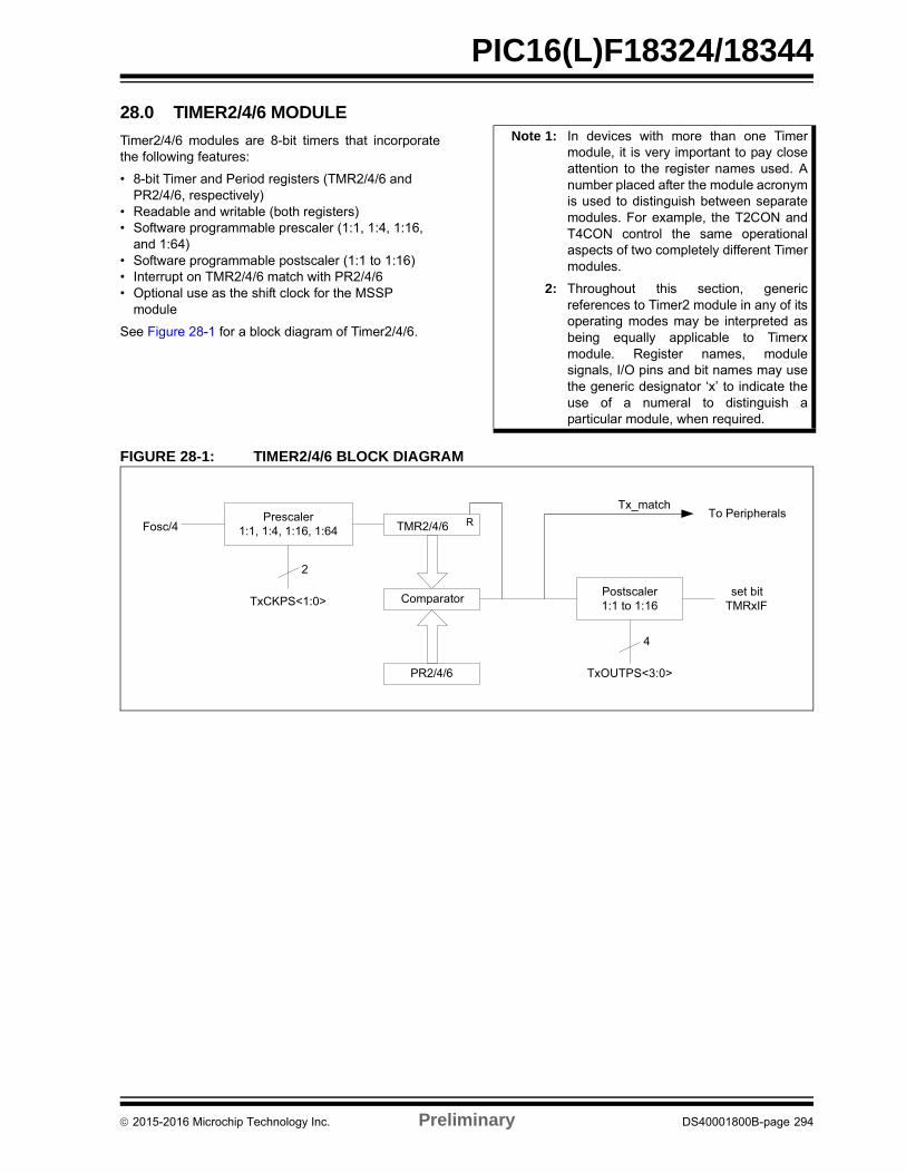
PIC16(L)F18324/18344
28.0 TIMER2/4/6 MODULE
Timer2/4/6 modules are 8-bit timers that incorporatethe following features:
• 8-bit Timer and Period registers (TMR2/4/6 and PR2/4/6, respectively)
• Readable and writable (both registers)• Software programmable prescaler (1:1, 1:4, 1:16,
and 1:64)• Software programmable postscaler (1:1 to 1:16)• Interrupt on TMR2/4/6 match with PR2/4/6• Optional use as the shift clock for the MSSP
module
See Figure 28-1 for a block diagram of Timer2/4/6.
FIGURE 28-1: TIMER2/4/6 BLOCK DIAGRAM
Note 1: In devices with more than one Timermodule, it is very important to pay closeattention to the register names used. Anumber placed after the module acronymis used to distinguish between separatemodules. For example, the T2CON andT4CON control the same operationalaspects of two completely different Timermodules.
2: Throughout this section, genericreferences to Timer2 module in any of itsoperating modes may be interpreted asbeing equally applicable to Timerxmodule. Register names, modulesignals, I/O pins and bit names may usethe generic designator ‘x’ to indicate theuse of a numeral to distinguish aparticular module, when required.
Prescaler1:1, 1:4, 1:16, 1:64Fosc/4
2
T CKPS<1:0> Comparator Postscaler1:1 to 1:16
4
T OUTPS<3:0>
set bitTMR IF
TMR2 R
PR2
T _matchTo Peripherals
2015-2016 Microchip Technology Inc. Preliminary DS40001800B-page 294
PIC16(L)F18324/18344
28.1 Timer2 Operation
The clock input to the Timer2 modules is the systeminstruction clock (FOSC/4).
A 4-bit counter/prescaler on the clock input allows directinput, divide-by-4 and divide-by-16 prescale options.These options are selected by the prescaler control bits,T2CKPS<1:0> of the T2CON register. The value ofTMR2 is compared to that of the Period register, PR2, oneach clock cycle. When the two values match, thecomparator generates a match signal as the timeroutput. This signal also resets the value of TMR2 to 00hon the next cycle and drives the outputcounter/postscaler (see Section 28.2 “Timer2Interrupt”).
The TMR2 and PR2 registers are both directly readableand writable. The TMR2 register is cleared on anydevice Reset, whereas the PR2 register initializes toFFh. Both the prescaler and postscaler counters arecleared on the following events:
• A write to the TMR2 register• A write to the T2CON register• Power-on Reset (POR)• Brown-out Reset (BOR)• MCLR Reset• Watchdog Timer (WDT) Reset• Stack Overflow Reset• Stack Underflow Reset• RESET Instruction
28.2 Timer2 Interrupt
Timer2 can also generate an optional device interrupt.The Timer2 output signal (TMR2-to-PR2 match)provides the input for the 4-bit counter/postscaler. Thiscounter generates the TMR2 match interrupt flag whichis latched in TMR2IF of the PIR1 register. The interruptis enabled by setting the TMR2 Match Interrupt Enablebit, TMR2IE, of the PIE1 register.
A range of 16 postscale options (from 1:1 through 1:16inclusive) can be selected with the postscaler controlbits, T2OUTPS<3:0>, of the T2CON register.
28.3 Timer2 Output
The unscaled output of TMR2 is available primarily tothe CCP modules, where it is used as a time base foroperations in PWM mode.
Timer2 can be optionally used as the shift clock sourcefor the MSSP module operating in SPI mode.Additional information is provided in Section 30.0“Master Synchronous Serial Port (MSSP1) Module”
28.4 Timer2 Operation During Sleep
The Timer2 timers cannot be operated while theprocessor is in Sleep mode. The contents of the TMR2and PR2 registers will remain unchanged while theprocessor is in Sleep mode.
Note: TMR2 is not cleared when T2CON iswritten.
2015-2016 Microchip Technology Inc. Preliminary DS40001800B-page 295
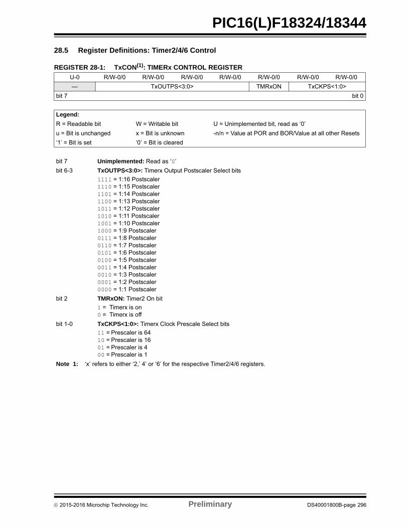
PIC16(L)F18324/18344
28.5 Register Definitions: Timer2/4/6 Control
REGISTER 28-1: TxCON(1): TIMERx CONTROL REGISTER
U-0 R/W-0/0 R/W-0/0 R/W-0/0 R/W-0/0 R/W-0/0 R/W-0/0 R/W-0/0
— TxOUTPS<3:0> TMRxON TxCKPS<1:0>
bit 7 bit 0
Legend:
R = Readable bit W = Writable bit U = Unimplemented bit, read as ‘0’
u = Bit is unchanged x = Bit is unknown -n/n = Value at POR and BOR/Value at all other Resets
‘1’ = Bit is set ‘0’ = Bit is cleared
bit 7 Unimplemented: Read as ‘0’
bit 6-3 TxOUTPS<3:0>: Timerx Output Postscaler Select bits
1111 = 1:16 Postscaler1110 = 1:15 Postscaler1101 = 1:14 Postscaler1100 = 1:13 Postscaler1011 = 1:12 Postscaler1010 = 1:11 Postscaler1001 = 1:10 Postscaler1000 = 1:9 Postscaler0111 = 1:8 Postscaler0110 = 1:7 Postscaler0101 = 1:6 Postscaler0100 = 1:5 Postscaler0011 = 1:4 Postscaler0010 = 1:3 Postscaler0001 = 1:2 Postscaler0000 = 1:1 Postscaler
bit 2 TMRxON: Timer2 On bit
1 = Timerx is on0 = Timerx is off
bit 1-0 TxCKPS<1:0>: Timerx Clock Prescale Select bits
11 = Prescaler is 6410 = Prescaler is 1601 = Prescaler is 400 = Prescaler is 1
Note 1: ‘x’ refers to either ‘2,’ 4’ or ‘6’ for the respective Timer2/4/6 registers.
2015-2016 Microchip Technology Inc. Preliminary DS40001800B-page 296
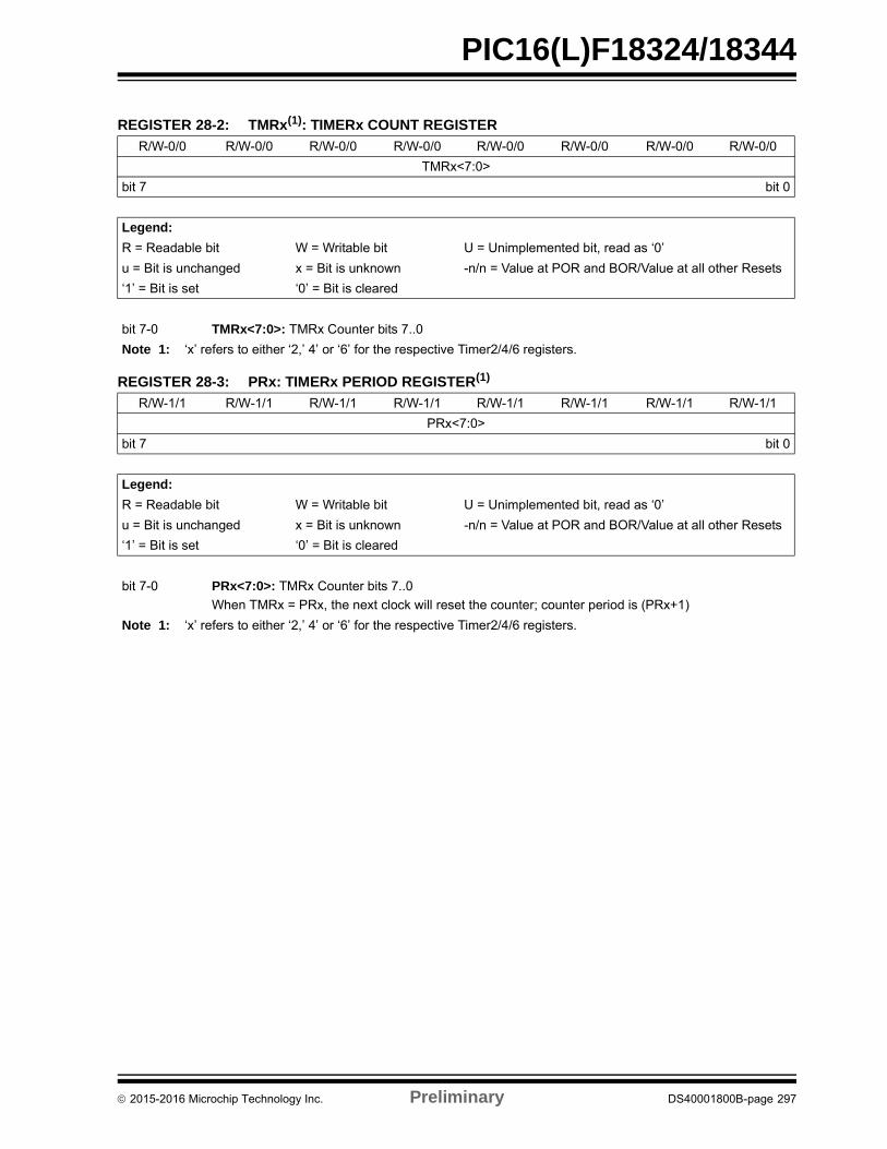
PIC16(L)F18324/18344
REGISTER 28-3: PRx: TIMERx PERIOD REGISTER(1)
REGISTER 28-2: TMRx(1): TIMERx COUNT REGISTER
R/W-0/0 R/W-0/0 R/W-0/0 R/W-0/0 R/W-0/0 R/W-0/0 R/W-0/0 R/W-0/0
TMRx<7:0>
bit 7 bit 0
Legend:
R = Readable bit W = Writable bit U = Unimplemented bit, read as ‘0’
u = Bit is unchanged x = Bit is unknown -n/n = Value at POR and BOR/Value at all other Resets
‘1’ = Bit is set ‘0’ = Bit is cleared
bit 7-0 TMRx<7:0>: TMRx Counter bits 7..0
Note 1: ‘x’ refers to either ‘2,’ 4’ or ‘6’ for the respective Timer2/4/6 registers.
R/W-1/1 R/W-1/1 R/W-1/1 R/W-1/1 R/W-1/1 R/W-1/1 R/W-1/1 R/W-1/1
PRx<7:0>
bit 7 bit 0
Legend:
R = Readable bit W = Writable bit U = Unimplemented bit, read as ‘0’
u = Bit is unchanged x = Bit is unknown -n/n = Value at POR and BOR/Value at all other Resets
‘1’ = Bit is set ‘0’ = Bit is cleared
bit 7-0 PRx<7:0>: TMRx Counter bits 7..0
When TMRx = PRx, the next clock will reset the counter; counter period is (PRx+1)
Note 1: ‘x’ refers to either ‘2,’ 4’ or ‘6’ for the respective Timer2/4/6 registers.
2015-2016 Microchip Technology Inc. Preliminary DS40001800B-page 297
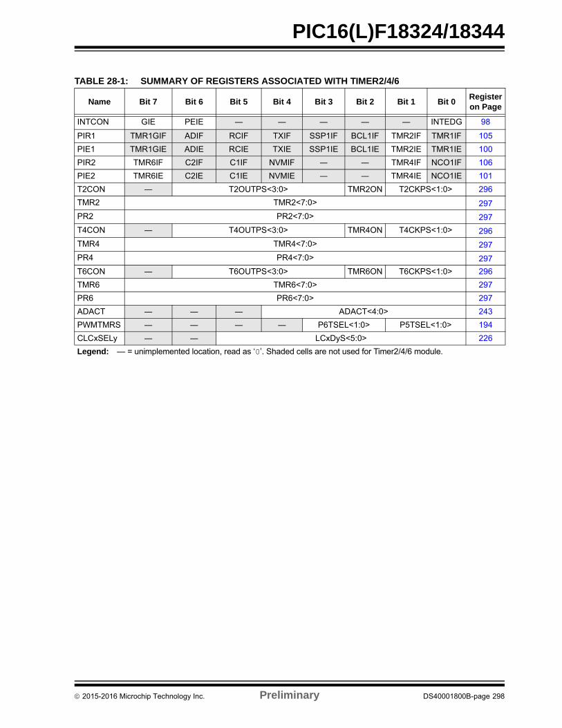
PIC16(L)F18324/18344
TABLE 28-1: SUMMARY OF REGISTERS ASSOCIATED WITH TIMER2/4/6
Name Bit 7 Bit 6 Bit 5 Bit 4 Bit 3 Bit 2 Bit 1 Bit 0Register on Page
INTCON GIE PEIE ― ― ― ― ― INTEDG 98
PIR1 TMR1GIF ADIF RCIF TXIF SSP1IF BCL1IF TMR2IF TMR1IF 105
PIE1 TMR1GIE ADIE RCIE TXIE SSP1IE BCL1IE TMR2IE TMR1IE 100
PIR2 TMR6IF C2IF C1IF NVMIF ― ― TMR4IF NCO1IF 106
PIE2 TMR6IE C2IE C1IE NVMIE ― ― TMR4IE NCO1IE 101
T2CON ― T2OUTPS<3:0> TMR2ON T2CKPS<1:0> 296
TMR2 TMR2<7:0> 297
PR2 PR2<7:0> 297
T4CON ― T4OUTPS<3:0> TMR4ON T4CKPS<1:0> 296
TMR4 TMR4<7:0> 297
PR4 PR4<7:0> 297
T6CON ― T6OUTPS<3:0> TMR6ON T6CKPS<1:0> 296
TMR6 TMR6<7:0> 297
PR6 PR6<7:0> 297
ADACT ― ― ― ADACT<4:0> 243
PWMTMRS ― ― ― ― P6TSEL<1:0> P5TSEL<1:0> 194
CLCxSELy ― ― LCxDyS<5:0> 226
Legend: — = unimplemented location, read as ‘0’. Shaded cells are not used for Timer2/4/6 module.
2015-2016 Microchip Technology Inc. Preliminary DS40001800B-page 298
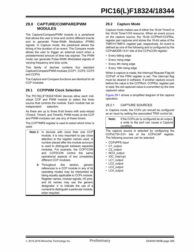
PIC16(L)F18324/18344
29.0 CAPTURE/COMPARE/PWM MODULES
The Capture/Compare/PWM module is a peripheralthat allows the user to time and control different eventsand to generate Pulse-Width Modulation (PWM)signals. In Capture mode, the peripheral allows thetiming of the duration of an event. The Compare modeallows the user to trigger an external event when apredetermined amount of time has expired. The PWMmode can generate Pulse-Width Modulated signals ofvarying frequency and duty cycle.
This family of devices contains four standardCapture/Compare/PWM modules (CCP1, CCP2, CCP3and CCP4).
The Capture and Compare functions are identical for allCCP modules.
29.1 CCP/PWM Clock Selection
The PIC16(L)F18324/18344 devices allow each indi-vidual CCP and PWM module to select the timersource that controls the module. Each module has anindependent selection.
As there are up to three 8-bit timers with auto-reload(Timer2, Timer4, and Timer6), PWM mode on the CCPand PWM modules can use any of these timers.
The CCPTMRS register is used to select which timer isused.
29.2 Capture Mode
Capture mode makes use of either the 16-bit Timer0 orthe 16-bit Timer1/3/5 resource. When an event occurson the capture source, the 16-bit CCPRxH:CCPRxLregister pair captures and stores the 16-bit value of theTMR1H:TMR1L register pair, respectively. An event isdefined as one of the following and is configured by theCCPxMODE<3:0> bits of the CCPxCON register:
• Every falling edge
• Every rising edge
• Every 4th rising edge
• Every 16th rising edge
When a capture is made, the Interrupt Request Flag bitCCPxIF of the PIR4 register is set. The interrupt flagmust be cleared in software. If another capture occursbefore the value in the CCPRxH, CCPRxL register pairis read, the old captured value is overwritten by the newcaptured value.
Figure 29-1 shows a simplified diagram of the captureoperation.
29.2.1 CAPTURE SOURCES
In Capture mode, the CCPx pin should be configuredas an input by setting the associated TRIS control bit.
The capture source is selected by configuring theCCPxCTS<3:0> bits of the CCPxCAP register.The following sources can be selected:
• CCPxPPS input• C1_output• C2_output• NCO_output• IOC_interrupt• LC1_output• LC2_output• LC3_output• LC4_output
Note 1: In devices with more than one CCPmodule, it is very important to pay closeattention to the register names used. Anumber placed after the module acronymis used to distinguish between separatemodules. For example, the CCP1CONand CCP2CON control the sameoperational aspects of two completelydifferent CCP modules.
2: Throughout this section, genericreferences to a CCP module in any of itsoperating modes may be interpreted asbeing equally applicable to CCPx module.Register names, module signals, I/O pins,and bit names may use the genericdesignator ‘x’ to indicate the use of anumeral to distinguish a particular module,when required.
Note: If the CCPx pin is configured as an output,a write to the port can cause a Capturecondition.
2015-2016 Microchip Technology Inc. Preliminary DS40001800B-page 299
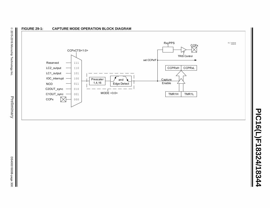
2
01
5-2
01
6 M
icroch
ip T
ech
no
log
y Inc.
Prelim
inary
DS
40
00
18
00
B-p
ag
e 3
00
PIC
16(L)F
18324/18344
FIG
Rev. 10-000158I8/29/2016
xL
1L
CCPx
ol
URE 29-1: CAPTURE MODE OPERATION BLOCK DIAGRAM
CCPRxH CCPR
TMR1H TMR
Prescaler1,4,16
TRIS Contrset CCPxIF
CCPx
MODE <3:0>
andEdge Detect
C1OUT_sync
C2OUT_sync
IOC_interrupt
RxyPPS
CCPxCTS<1:0>
000
011010001
100101110111
NCO
LC1_output
LC2_output
Reserved
Capture Enable
PIC16(L)F18324/18344
29.2.2 TIMER1/3/5 MODE RESOURCE
Timer1/3/5 must be running in Timer mode orSynchronized Counter mode for the CCP module to usethe capture feature. In Asynchronous Counter mode, thecapture operation may not work.
See Section 27.0 “Timer1/3/5 Module with GateControl” for more information on configuringTimer1/3/5.
29.2.3 SOFTWARE INTERRUPT MODE
When the Capture mode is changed, a false captureinterrupt may be generated. The user should keep theCCPxIE interrupt enable bit of the PIE4 register clear toavoid false interrupts. Additionally, the user shouldclear the CCPxIF interrupt flag bit of the PIR4 registerfollowing any change in Operating mode.
29.2.4 CCP PRESCALER
There are four prescaler settings specified by theCCPxMODE<3:0> bits of the CCPxCON register.Whenever the CCP module is turned off, or the CCPmodule is not in Capture mode, the prescaler counteris cleared. Any Reset will clear the prescaler counter.
Switching from one capture prescaler to another does notclear the prescaler and may generate a false interrupt. Toavoid this unexpected operation, turn the module off byclearing the CCPxCON register before changing theprescaler. Example 29-1 demonstrates the code toperform this function.
EXAMPLE 29-1: CHANGING BETWEEN CAPTURE PRESCALERS
29.2.5 CAPTURE DURING SLEEP
Capture mode depends upon the Timer1/3/5 module forproper operation. There are two options for driving theTimer1/3/5 module in Capture mode. It can be driven bythe instruction clock (FOSC/4), or by an external clocksource.
When Timer1/3/5 is clocked by FOSC/4, Timer1/3/5 willnot increment during Sleep. When the device wakesfrom Sleep, Timer1/3/5 will continue from its previousstate.
Capture mode will operate during Sleep whenTimer1/3/5 is clocked by an external clock source.
Note: Clocking Timer1/3/5 from the system clock(FOSC) should not be used in Capturemode. In order for Capture mode torecognize the trigger event on the CCPxpin, Timer1/3/5 must be clocked from theinstruction clock (FOSC/4) or from anexternal clock source.
BANKSEL CCPxCON ;Set Bank bits to point;to CCPxCON
CLRF CCPxCON ;Turn CCP module offMOVLW NEW_CAPT_PS;Load the W reg with
;the new prescaler;move value and CCP ON
MOVWF CCPxCON ;Load CCPxCON with this;value
2015-2016 Microchip Technology Inc. Preliminary DS40001800B-page 301
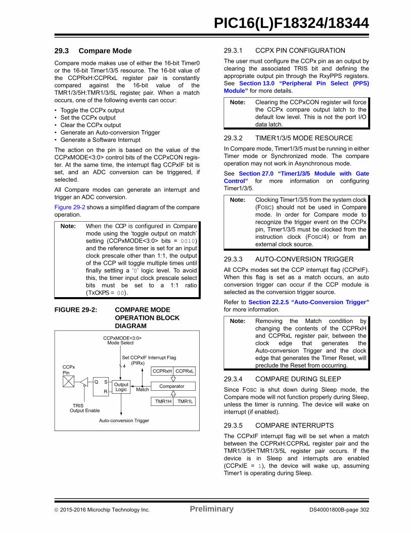
PIC16(L)F18324/18344
29.3 Compare Mode
Compare mode makes use of either the 16-bit Timer0or the 16-bit Timer1/3/5 resource. The 16-bit value ofthe CCPRxH:CCPRxL register pair is constantlycompared against the 16-bit value of theTMR1/3/5H:TMR1/3/5L register pair. When a matchoccurs, one of the following events can occur:
• Toggle the CCPx output• Set the CCPx output• Clear the CCPx output• Generate an Auto-conversion Trigger• Generate a Software Interrupt
The action on the pin is based on the value of theCCPxMODE<3:0> control bits of the CCPxCON regis-ter. At the same time, the interrupt flag CCPxIF bit isset, and an ADC conversion can be triggered, ifselected.
All Compare modes can generate an interrupt andtrigger an ADC conversion.
Figure 29-2 shows a simplified diagram of the compareoperation.
FIGURE 29-2: COMPARE MODE OPERATION BLOCK DIAGRAM
29.3.1 CCPX PIN CONFIGURATION
The user must configure the CCPx pin as an output byclearing the associated TRIS bit and defining theappropriate output pin through the RxyPPS registers.See Section 13.0 “Peripheral Pin Select (PPS)Module” for more details.
29.3.2 TIMER1/3/5 MODE RESOURCE
In Compare mode, Timer1/3/5 must be running in eitherTimer mode or Synchronized mode. The compareoperation may not work in Asynchronous mode.
See Section 27.0 “Timer1/3/5 Module with GateControl” for more information on configuringTimer1/3/5.
29.3.3 AUTO-CONVERSION TRIGGER
All CCPx modes set the CCP interrupt flag (CCPxIF).When this flag is set as a match occurs, an autoconversion trigger can occur if the CCP module isselected as the conversion trigger source.
Refer to Section 22.2.5 “Auto-Conversion Trigger”for more information.
29.3.4 COMPARE DURING SLEEP
Since FOSC is shut down during Sleep mode, theCompare mode will not function properly during Sleep,unless the timer is running. The device will wake oninterrupt (if enabled).
29.3.5 COMPARE INTERRUPTS
The CCPxIF interrupt flag will be set when a matchbetween the CCPRxH:CCPRxL register pair and theTMR1/3/5H:TMR1/3/5L register pair occurs. If thedevice is in Sleep and interrupts are enabled(CCPxIE = 1), the device will wake up, assumingTimer1 is operating during Sleep.
Note: When the CCP is configured in Comparemode using the ‘toggle output on match’setting (CCPxMODE<3:0> bits = 0010)and the reference timer is set for an inputclock prescale other than 1:1, the outputof the CCP will toggle multiple times untilfinally settling a ‘0’ logic level. To avoidthis, the timer input clock prescale selectbits must be set to a 1:1 ratio(TxCKPS = 00).
CCPRxH CCPRxL
TMR1H TMR1L
ComparatorQ S
R
OutputLogic
Auto-conversion Trigger
Set CCPxIF Interrupt Flag(PIRx)
Match
TRIS
CCPxMODE<3:0>Mode Select
Output Enable
PinCCPx 4
Note: Clearing the CCPxCON register will forcethe CCPx compare output latch to thedefault low level. This is not the port I/Odata latch.
Note: Clocking Timer1/3/5 from the system clock(FOSC) should not be used in Comparemode. In order for Compare mode torecognize the trigger event on the CCPxpin, Timer1/3/5 must be clocked from theinstruction clock (FOSC/4) or from anexternal clock source.
Note: Removing the Match condition bychanging the contents of the CCPRxHand CCPRxL register pair, between theclock edge that generates theAuto-conversion Trigger and the clockedge that generates the Timer Reset, willpreclude the Reset from occurring.
2015-2016 Microchip Technology Inc. Preliminary DS40001800B-page 302
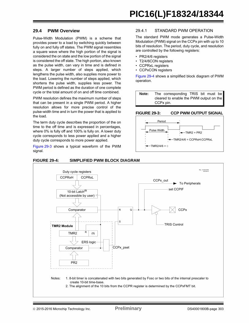
PIC16(L)F18324/18344
29.4 PWM Overview
Pulse-Width Modulation (PWM) is a scheme thatprovides power to a load by switching quickly betweenfully on and fully off states. The PWM signal resemblesa square wave where the high portion of the signal isconsidered the on state and the low portion of the signalis considered the off state. The high portion, also knownas the pulse width, can vary in time and is defined insteps. A larger number of steps applied, whichlengthens the pulse width, also supplies more power tothe load. Lowering the number of steps applied, whichshortens the pulse width, supplies less power. ThePWM period is defined as the duration of one completecycle or the total amount of on and off time combined.
PWM resolution defines the maximum number of stepsthat can be present in a single PWM period. A higherresolution allows for more precise control of thepulse-width time and in turn the power that is applied tothe load.
The term duty cycle describes the proportion of the ontime to the off time and is expressed in percentages,where 0% is fully off and 100% is fully on. A lower dutycycle corresponds to less power applied and a higherduty cycle corresponds to more power applied.
Figure 29-3 shows a typical waveform of the PWMsignal.
29.4.1 STANDARD PWM OPERATION
The standard PWM mode generates a Pulse-WidthModulation (PWM) signal on the CCPx pin with up to 10bits of resolution. The period, duty cycle, and resolutionare controlled by the following registers:
• PR2/4/6 registers• T2/4/6CON registers• CCPRxL registers• CCPxCON registers
Figure 29-4 shows a simplified block diagram of PWMoperation.
FIGURE 29-3: CCP PWM OUTPUT SIGNAL
FIGURE 29-4: SIMPLIFIED PWM BLOCK DIAGRAM
Note: The corresponding TRIS bit must becleared to enable the PWM output on theCCPx pin.
Period
Pulse Width
TMR2/4/6 = 0
TMR2/4/6 = CCPRxH:CCPRxL
TMR2 = PR2
Rev. 10-000157B2/27/2014
CCPRxH
Duty cycle registers
10-bit Latch(2)
(Not accessible by user)
Comparator
Comparator
PR2
(1)TMR2
TMR2 Module
CCPx
CCPx_outTo Peripherals
R
TRIS Control
R
S
Q
CCPRxL
set CCPIF
CCPx_psetERS logic
Notes: 1. 8-bit timer is concatenated with two bits generated by Fosc or two bits of the internal prescaler to create 10-bit time-base.
2. The alignment of the 10 bits from the CCPR register is determined by the CCPxFMT bit.
2015-2016 Microchip Technology Inc. Preliminary DS40001800B-page 303
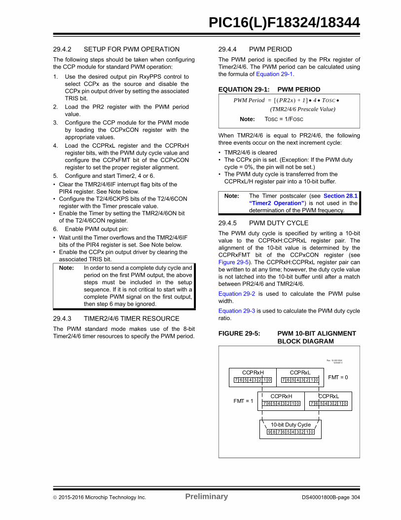
PIC16(L)F18324/18344
29.4.2 SETUP FOR PWM OPERATION
The following steps should be taken when configuringthe CCP module for standard PWM operation:
1. Use the desired output pin RxyPPS control toselect CCPx as the source and disable theCCPx pin output driver by setting the associatedTRIS bit.
2. Load the PR2 register with the PWM periodvalue.
3. Configure the CCP module for the PWM modeby loading the CCPxCON register with theappropriate values.
4. Load the CCPRxL register and the CCPRxHregister bits, with the PWM duty cycle value andconfigure the CCPxFMT bit of the CCPxCONregister to set the proper register alignment.
5. Configure and start Timer2, 4 or 6.
• Clear the TMR2/4/6IF interrupt flag bits of the PIR4 register. See Note below.
• Configure the T2/4/6CKPS bits of the T2/4/6CON register with the Timer prescale value.
• Enable the Timer by setting the TMR2/4/6ON bit of the T2/4/6CON register.
6. Enable PWM output pin:
• Wait until the Timer overflows and the TMR2/4/6IF bits of the PIR4 register is set. See Note below.
• Enable the CCPx pin output driver by clearing the associated TRIS bit.
29.4.3 TIMER2/4/6 TIMER RESOURCE
The PWM standard mode makes use of the 8-bitTimer2/4/6 timer resources to specify the PWM period.
29.4.4 PWM PERIOD
The PWM period is specified by the PRx register ofTimer2/4/6. The PWM period can be calculated usingthe formula of Equation 29-1.
EQUATION 29-1: PWM PERIOD
When TMR2/4/6 is equal to PR2/4/6, the followingthree events occur on the next increment cycle:
• TMR2/4/6 is cleared• The CCPx pin is set. (Exception: If the PWM duty
cycle = 0%, the pin will not be set.)• The PWM duty cycle is transferred from the
CCPRxL/H register pair into a 10-bit buffer.
29.4.5 PWM DUTY CYCLE
The PWM duty cycle is specified by writing a 10-bitvalue to the CCPRxH:CCPRxL register pair. Thealignment of the 10-bit value is determined by theCCPRxFMT bit of the CCPxCON register (seeFigure 29-5). The CCPRxH:CCPRxL register pair canbe written to at any time; however, the duty cycle valueis not latched into the 10-bit buffer until after a matchbetween PR2/4/6 and TMR2/4/6.
Equation 29-2 is used to calculate the PWM pulsewidth.
Equation 29-3 is used to calculate the PWM duty cycleratio.
FIGURE 29-5: PWM 10-BIT ALIGNMENT BLOCK DIAGRAM
Note: In order to send a complete duty cycle andperiod on the first PWM output, the abovesteps must be included in the setupsequence. If it is not critical to start with acomplete PWM signal on the first output,then step 6 may be ignored.
Note: The Timer postscaler (see Section 28.1“Timer2 Operation”) is not used in thedetermination of the PWM frequency.
PWM Period PR2x 1+ 4 TOSC =
(TMR2/4/6 Prescale Value)
Note: TOSC = 1/FOSC
Rev. 10-000 160A12/9/201 3
7 6 5 4 3 2 1 0 7 6 5 4 3 2 1 0CCPRxH CCPRxL
7 6 5 4 3 2 1 0 7 6 5 4 3 2 1 0CCPRxH CCPRxL
FMT = 0
FMT = 1
7 6 5 4 3 2 1 09 810-bit Duty Cycle
2015-2016 Microchip Technology Inc. Preliminary DS40001800B-page 304
PIC16(L)F18324/18344
EQUATION 29-2: PULSE WIDTH
EQUATION 29-3: DUTY CYCLE RATIO
The CCPRxH:CCPRxL register pair and a 2-bit internallatch are used to double buffer the PWM duty cycle.This double buffering provides glitchless PWMoperation.
The 8-bit timer TMR2/4/6 register is concatenated witheither the 2-bit internal system clock (FOSC), or two bitsof the prescaler, to create the 10-bit time base. Thesystem clock is used if the Timer2/4/6 prescaler is set to1:1.
When the 10-bit time base matches theCCPRxH:CCPRxL register pair, then the CCPx pin iscleared (see Figure 29-4).
29.4.6 PWM RESOLUTION
PWM resolution, expressed in number of bits, definesthe maximum number of discrete steps that can bepresent in a single PWM period. For example, a 10-bitresolution will result in 1024 discrete steps, whereas an8-bit resolution will result in 256 discrete steps.
The maximum PWM resolution is ten bits when PRx is255. The resolution is a function of the PRx registervalue as shown by Equation 29-4.
EQUATION 29-4: PWM RESOLUTION
29.4.7 OPERATION IN SLEEP MODE
In Sleep mode, the TMR2/4/6 register will not incre-ment and the state of the module will not change. If theCCPx pin is driving a value, it will continue to drive thatvalue. When the device wakes up, TMR2/4/6 willcontinue from its previous state.
29.4.8 CHANGES IN SYSTEM CLOCK FREQUENCY
The PWM frequency is derived from the system clockfrequency. Any changes in the system clock frequencywill result in changes to the PWM frequency. SeeSection 7.0 “Oscillator Module” for additionaldetails.
29.4.9 EFFECTS OF RESET
Any Reset will force all ports to Input mode and theCCP registers to their Reset states.
Pulse Width CCPRxH:CCPRxL register pair =
TOSC (TMR2 Prescale Value)
Duty Cycle RatioCCPRxH:CCPRxL register pair
4 PR2 1+ ----------------------------------------------------------------------------------=
Note: If the pulse-width value is greater than theperiod the assigned PWM pin(s) willremain unchanged.
Resolution4 PRx 1+ log
2 log------------------------------------------ bits=
TABLE 29-1: EXAMPLE PWM FREQUENCIES AND RESOLUTIONS (FOSC = 20 MHz)
PWM Frequency 1.22 kHz 4.88 kHz 19.53 kHz 78.12 kHz 156.3 kHz 208.3 kHz
Timer Prescale 16 4 1 1 1 1
PRx Value 0xFF 0xFF 0xFF 0x3F 0x1F 0x17
Maximum Resolution (bits) 10 10 10 8 7 6.6
TABLE 29-2: EXAMPLE PWM FREQUENCIES AND RESOLUTIONS (FOSC = 8 MHz)
PWM Frequency 1.22 kHz 4.90 kHz 19.61 kHz 76.92 kHz 153.85 kHz 200.0 kHz
Timer Prescale 16 4 1 1 1 1
PRx Value 0x65 0x65 0x65 0x19 0x0C 0x09
Maximum Resolution (bits) 8 8 8 6 5 5
2015-2016 Microchip Technology Inc. Preliminary DS40001800B-page 305
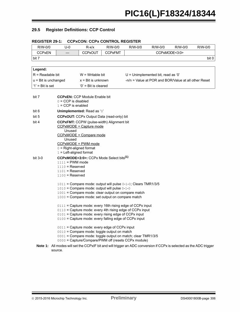
PIC16(L)F18324/18344
29.5 Register Definitions: CCP Control
REGISTER 29-1: CCPxCON: CCPx CONTROL REGISTER
R/W-0/0 U-0 R-x/x R/W-0/0 R/W-0/0 R/W-0/0 R/W-0/0 R/W-0/0
CCPxEN — CCPxOUT CCPxFMT CCPxMODE<3:0>
bit 7 bit 0
Legend:
R = Readable bit W = Writable bit U = Unimplemented bit, read as ‘0’
u = Bit is unchanged x = Bit is unknown -n/n = Value at POR and BOR/Value at all other Reset
‘1’ = Bit is set ‘0’ = Bit is cleared
bit 7 CCPxEN: CCP Module Enable bit0 = CCP is disabled1 = CCP is enabled
bit 6 Unimplemented: Read as ‘0’
bit 5 CCPxOUT: CCPx Output Data (read-only) bit
bit 4 CCPxFMT: CCPW (pulse-width) Alignment bitCCPxMODE = Capture mode
UnusedCCPxMODE = Compare mode
UnusedCCPxMODE = PWM mode0 = Right-aligned format1 = Left-aligned format
bit 3-0 CCPxMODE<3:0>: CCPx Mode Select bits(1)
1111 = PWM mode1110 = Reserved1101 = Reserved1100 = Reserved
1011 = Compare mode: output will pulse 0-1-0; Clears TMR1/3/51010 = Compare mode: output will pulse 0-1-01001 = Compare mode: clear output on compare match1000 = Compare mode: set output on compare match
0111 = Capture mode: every 16th rising edge of CCPx input0110 = Capture mode: every 4th rising edge of CCPx input0101 = Capture mode: every rising edge of CCPx input0100 = Capture mode: every falling edge of CCPx input
0011 = Capture mode: every edge of CCPx input0010 = Compare mode: toggle output on match0001 = Compare mode: toggle output on match; clear TMR1/3/50000 = Capture/Compare/PWM off (resets CCPx module)
Note 1: All modes will set the CCPxIF bit and will trigger an ADC conversion if CCPx is selected as the ADC triggersource.
2015-2016 Microchip Technology Inc. Preliminary DS40001800B-page 306
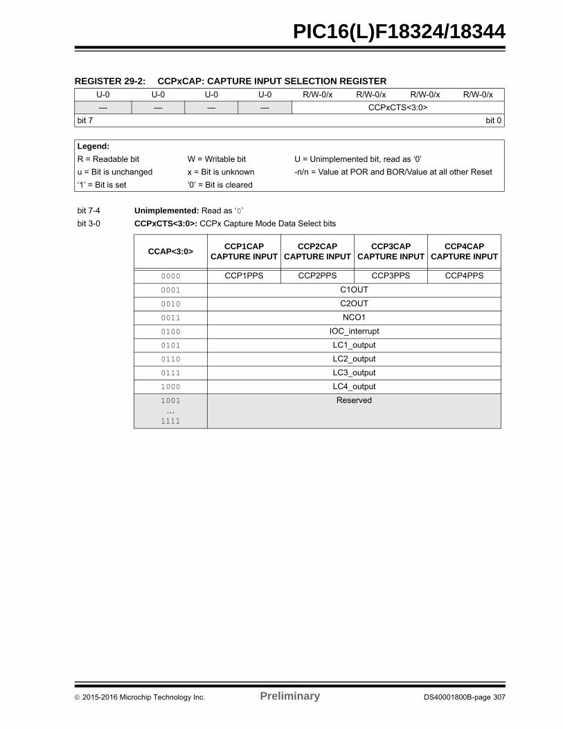
PIC16(L)F18324/18344
REGISTER 29-2: CCPxCAP: CAPTURE INPUT SELECTION REGISTER
U-0 U-0 U-0 U-0 R/W-0/x R/W-0/x R/W-0/x R/W-0/x
— — — — CCPxCTS<3:0>
bit 7 bit 0
Legend:
R = Readable bit W = Writable bit U = Unimplemented bit, read as ‘0’
u = Bit is unchanged x = Bit is unknown -n/n = Value at POR and BOR/Value at all other Reset
‘1’ = Bit is set ‘0’ = Bit is cleared
bit 7-4 Unimplemented: Read as ‘0’
bit 3-0 CCPxCTS<3:0>: CCPx Capture Mode Data Select bits
CCAP<3:0>CCP1CAP
CAPTURE INPUTCCP2CAP
CAPTURE INPUTCCP3CAP
CAPTURE INPUTCCP4CAP
CAPTURE INPUT
0000 CCP1PPS CCP2PPS CCP3PPS CCP4PPS
0001 C1OUT
0010 C2OUT
0011 NCO1
0100 IOC_interrupt
0101 LC1_output
0110 LC2_output
0111 LC3_output
1000 LC4_output
1001…
1111
Reserved
2015-2016 Microchip Technology Inc. Preliminary DS40001800B-page 307
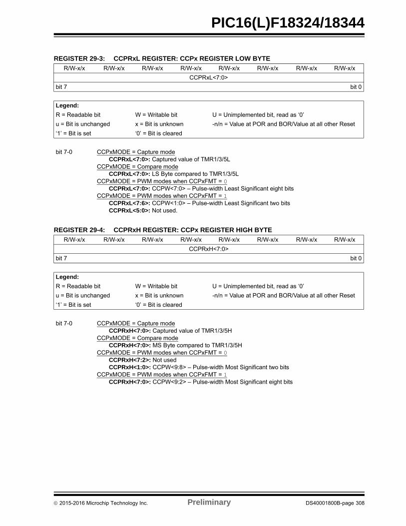
PIC16(L)F18324/18344
REGISTER 29-3: CCPRxL REGISTER: CCPx REGISTER LOW BYTE
R/W-x/x R/W-x/x R/W-x/x R/W-x/x R/W-x/x R/W-x/x R/W-x/x R/W-x/x
CCPRxL<7:0>
bit 7 bit 0
Legend:
R = Readable bit W = Writable bit U = Unimplemented bit, read as ‘0’
u = Bit is unchanged x = Bit is unknown -n/n = Value at POR and BOR/Value at all other Reset
‘1’ = Bit is set ‘0’ = Bit is cleared
bit 7-0 CCPxMODE = Capture modeCCPRxL<7:0>: Captured value of TMR1/3/5L
CCPxMODE = Compare modeCCPRxL<7:0>: LS Byte compared to TMR1/3/5L
CCPxMODE = PWM modes when CCPxFMT = 0CCPRxL<7:0>: CCPW<7:0> – Pulse-width Least Significant eight bits
CCPxMODE = PWM modes when CCPxFMT = 1CCPRxL<7:6>: CCPW<1:0> – Pulse-width Least Significant two bitsCCPRxL<5:0>: Not used.
REGISTER 29-4: CCPRxH REGISTER: CCPx REGISTER HIGH BYTE
R/W-x/x R/W-x/x R/W-x/x R/W-x/x R/W-x/x R/W-x/x R/W-x/x R/W-x/x
CCPRxH<7:0>
bit 7 bit 0
Legend:
R = Readable bit W = Writable bit U = Unimplemented bit, read as ‘0’
u = Bit is unchanged x = Bit is unknown -n/n = Value at POR and BOR/Value at all other Reset
‘1’ = Bit is set ‘0’ = Bit is cleared
bit 7-0 CCPxMODE = Capture modeCCPRxH<7:0>: Captured value of TMR1/3/5H
CCPxMODE = Compare modeCCPRxH<7:0>: MS Byte compared to TMR1/3/5H
CCPxMODE = PWM modes when CCPxFMT = 0CCPRxH<7:2>: Not usedCCPRxH<1:0>: CCPW<9:8> – Pulse-width Most Significant two bits
CCPxMODE = PWM modes when CCPxFMT = 1CCPRxH<7:0>: CCPW<9:2> – Pulse-width Most Significant eight bits
2015-2016 Microchip Technology Inc. Preliminary DS40001800B-page 308
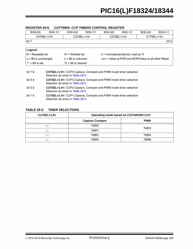
PIC16(L)F18324/18344
REGISTER 29-5: CCPTMRS: CCP TIMERS CONTROL REGISTER
R/W-0/0 R/W-1/1 R/W-0/0 R/W-1/1 R/W-0/0 R/W-1/1 R/W-0/0 R/W-1/1
C4TSEL<1:0> C3TSEL<1:0> C2TSEL<1:0> C1TSEL<1:0>
bit 7 bit 0
Legend:
R = Readable bit W = Writable bit U = Unimplemented bit, read as ‘0’
u = Bit is unchanged x = Bit is unknown -n/n = Value at POR and BOR/Value at all other Reset
‘1’ = Bit is set ‘0’ = Bit is cleared
bit 7-6 C4TSEL<1:0>: CCP4 Capture, Compare and PWM mode timer selectionSelection as show in Table 29-3.
bit 5-4 C3TSEL<1:0>: CCP3 Capture, Compare and PWM mode timer selectionSelection as show in Table 29-3.
bit 3-2 C2TSEL<1:0>: CCP2 Capture, Compare and PWM mode timer selectionSelection as show in Table 29-3.
bit 1-0 C1TSEL<1:0>: CCP1 Capture, Compare and PWM mode timer selectionSelection as show in Table 29-3.
TABLE 29-3: TIMER SELECTIONS
CxTSEL<1:0> Operating mode based on CCPxMODE<3:0>
Capture Compare PWM
00 TMR0TMR2
01 TMR1
10 TMR3 TMR4
11 TMR5 TMR6
2015-2016 Microchip Technology Inc. Preliminary DS40001800B-page 309
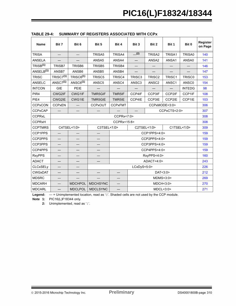
PIC16(L)F18324/18344
TABLE 29-4: SUMMARY OF REGISTERS ASSOCIATED WITH CCPx
Name Bit 7 Bit 6 Bit 5 Bit 4 Bit 3 Bit 2 Bit 1 Bit 0Register on Page
TRISA ― ― TRISA5 TRISA4 ―(2) TRISA2 TRISA1 TRISA0 140
ANSELA ― ― ANSA5 ANSA4 ― ANSA2 ANSA1 ANSA0 141
TRISB(1) TRISB7 TRISB6 TRISB5 TRISB4 ― ― ― ― 146
ANSELB(1) ANSB7 ANSB6 ANSB5 ANSB4 ― ― ― ― 147
TRISC TRISC7(1) TRISC6(1) TRISC5 TRISC4 TRISC3 TRISC2 TRISC1 TRISC0 153
ANSELC ANSC7(1) ANSC6(1) ANSC5 ANSC4 ANSC3 ANSC2 ANSC1 ANSC0 154
INTCON GIE PEIE ― ― ― ― ― INTEDG 98
PIR4 CWG2IF CWG1IF TMR5GIF TMR5IF CCP4IF CCP3IF CCP2IF CCP1IF 108
PIE4 CWG2IE CWG1IE TMR5GIE TMR5IE CCP4IE CCP3IE CCP2IE CCP1IE 103
CCPxCON CCPxEN ― CCPxOUT CCPxFMT CCPxMODE<3:0> 306
CCPxCAP ― ― ― ― ― CCPxCTS<2:0> 307
CCPRxL CCPRx<7:0> 308
CCPRxH CCPRx<15:8> 308
CCPTMRS C4TSEL<1:0> C3TSEL<1:0> C2TSEL<1:0> C1TSEL<1:0> 309
CCP1PPS ― ― ― CCP1PPS<4:0> 159
CCP2PPS ― ― ― CCP2PPS<4:0> 159
CCP3PPS ― ― ― CCP3PPS<4:0> 159
CCP4PPS ― ― ― CCP4PPS<4:0> 159
RxyPPS ― ― ― RxyPPS<4:0> 160
ADACT ― ― ― ADACT<4:0> 243
CLCxSELy ― ― LCxDyS<5:0> 226
CWGxDAT ― ― ― ― DAT<3:0> 212
MDSRC ― ― ― ― MDMS<3:0> 269
MDCARH ― MDCHPOL MDCHSYNC ― MDCH<3:0> 270
MDCARL ― MDCLPOL MDCLSYNC ― MDCL<3:0> 271
Legend: — = Unimplemented location, read as ‘0’. Shaded cells are not used by the CCP module.Note 1: PIC16(L)F18344 only.
2: Unimplemented, read as ‘1’.
2015-2016 Microchip Technology Inc. Preliminary DS40001800B-page 310
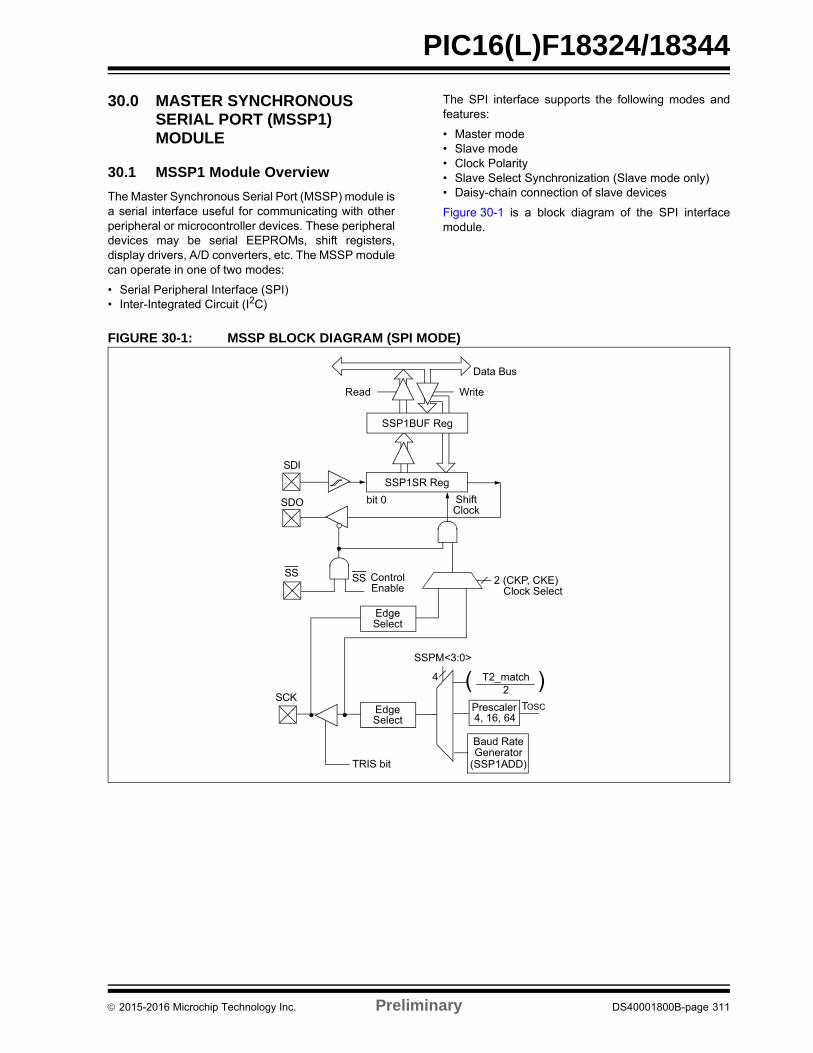
PIC16(L)F18324/18344
30.0 MASTER SYNCHRONOUS SERIAL PORT (MSSP1) MODULE
30.1 MSSP1 Module Overview
The Master Synchronous Serial Port (MSSP) module isa serial interface useful for communicating with otherperipheral or microcontroller devices. These peripheraldevices may be serial EEPROMs, shift registers,display drivers, A/D converters, etc. The MSSP modulecan operate in one of two modes:
• Serial Peripheral Interface (SPI)• Inter-Integrated Circuit (I2C)
The SPI interface supports the following modes andfeatures:
• Master mode• Slave mode• Clock Polarity• Slave Select Synchronization (Slave mode only)• Daisy-chain connection of slave devices
Figure 30-1 is a block diagram of the SPI interfacemodule.
FIGURE 30-1: MSSP BLOCK DIAGRAM (SPI MODE)
( )
Read Write
Data Bus
SSP1SR Reg
SSPM<3:0>
bit 0 ShiftClock
SS ControlEnable
EdgeSelect
Clock Select
T2_match2
EdgeSelect
2 (CKP, CKE)
4
TRIS bit
SDO
SSP1BUF Reg
SDI
SS
SCKTOSCPrescaler
4, 16, 64
Baud RateGenerator
(SSP1ADD)
2015-2016 Microchip Technology Inc. Preliminary DS40001800B-page 311
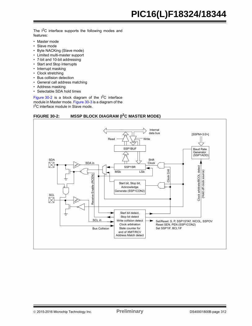
PIC16(L)F18324/18344
The I2C interface supports the following modes andfeatures:
• Master mode• Slave mode• Byte NACKing (Slave mode)• Limited multi-master support• 7-bit and 10-bit addressing• Start and Stop interrupts• Interrupt masking• Clock stretching• Bus collision detection• General call address matching• Address masking• Selectable SDA hold times
Figure 30-2 is a block diagram of the I2C interfacemodule in Master mode. Figure 30-3 is a diagram of theI2C interface module in Slave mode.
FIGURE 30-2: MSSP BLOCK DIAGRAM (I2C MASTER MODE)
Read Write
SSP1SR
Start bit, Stop bit,
Start bit detect,
SSP1BUF
Internaldata bus
Set/Reset: S, P, SSP1STAT, WCOL, SSPOV
ShiftClock
MSb LSb
SDA
AcknowledgeGenerate (SSP1CON2)
Stop bit detectWrite collision detect
Clock arbitrationState counter forend of XMIT/RCV
SCL
SCL in
Bus Collision
SDA in
Re
ceiv
e E
nab
le (
RC
EN
)
Clo
ck C
ntl
Clo
ck a
rbitr
ate
/BC
OL
dete
ct
(Hol
d of
f cl
ock
sour
ce)
[SSPM<3:0>]
Baud Rate
Reset SEN, PEN (SSP1CON2)
Generator(SSP1ADD)
Address Match detect
Set SSP1IF, BCL1IF
2015-2016 Microchip Technology Inc. Preliminary DS40001800B-page 312
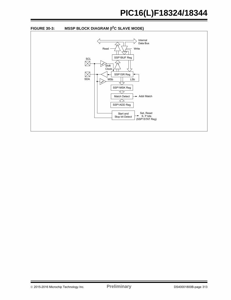
PIC16(L)F18324/18344
FIGURE 30-3: MSSP BLOCK DIAGRAM (I2C SLAVE MODE)
Read Write
SSP1SR Reg
Match Detect
SSP1ADD Reg
Start andStop bit Detect
SSP1BUF Reg
InternalData Bus
Addr Match
Set, ResetS, P bits
(SSP1STAT Reg)
SCL
SDA
ShiftClock
MSb LSb
SSP1MSK Reg
2015-2016 Microchip Technology Inc. Preliminary DS40001800B-page 313
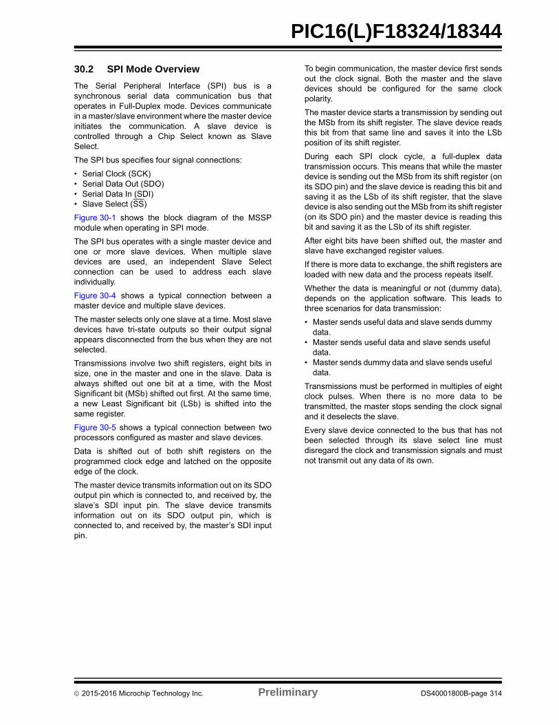
PIC16(L)F18324/18344
30.2 SPI Mode Overview
The Serial Peripheral Interface (SPI) bus is asynchronous serial data communication bus thatoperates in Full-Duplex mode. Devices communicatein a master/slave environment where the master deviceinitiates the communication. A slave device iscontrolled through a Chip Select known as SlaveSelect.
The SPI bus specifies four signal connections:
• Serial Clock (SCK)• Serial Data Out (SDO)• Serial Data In (SDI)• Slave Select (SS)
Figure 30-1 shows the block diagram of the MSSPmodule when operating in SPI mode.
The SPI bus operates with a single master device andone or more slave devices. When multiple slavedevices are used, an independent Slave Selectconnection can be used to address each slaveindividually.
Figure 30-4 shows a typical connection between amaster device and multiple slave devices.
The master selects only one slave at a time. Most slavedevices have tri-state outputs so their output signalappears disconnected from the bus when they are notselected.
Transmissions involve two shift registers, eight bits insize, one in the master and one in the slave. Data isalways shifted out one bit at a time, with the MostSignificant bit (MSb) shifted out first. At the same time,a new Least Significant bit (LSb) is shifted into thesame register.
Figure 30-5 shows a typical connection between twoprocessors configured as master and slave devices.
Data is shifted out of both shift registers on theprogrammed clock edge and latched on the oppositeedge of the clock.
The master device transmits information out on its SDOoutput pin which is connected to, and received by, theslave’s SDI input pin. The slave device transmitsinformation out on its SDO output pin, which isconnected to, and received by, the master’s SDI inputpin.
To begin communication, the master device first sendsout the clock signal. Both the master and the slavedevices should be configured for the same clockpolarity.
The master device starts a transmission by sending outthe MSb from its shift register. The slave device readsthis bit from that same line and saves it into the LSbposition of its shift register.
During each SPI clock cycle, a full-duplex datatransmission occurs. This means that while the masterdevice is sending out the MSb from its shift register (onits SDO pin) and the slave device is reading this bit andsaving it as the LSb of its shift register, that the slavedevice is also sending out the MSb from its shift register(on its SDO pin) and the master device is reading thisbit and saving it as the LSb of its shift register.
After eight bits have been shifted out, the master andslave have exchanged register values.
If there is more data to exchange, the shift registers areloaded with new data and the process repeats itself.
Whether the data is meaningful or not (dummy data),depends on the application software. This leads tothree scenarios for data transmission:
• Master sends useful data and slave sends dummy data.
• Master sends useful data and slave sends useful data.
• Master sends dummy data and slave sends useful data.
Transmissions must be performed in multiples of eightclock pulses. When there is no more data to betransmitted, the master stops sending the clock signaland it deselects the slave.
Every slave device connected to the bus that has notbeen selected through its slave select line mustdisregard the clock and transmission signals and mustnot transmit out any data of its own.
2015-2016 Microchip Technology Inc. Preliminary DS40001800B-page 314
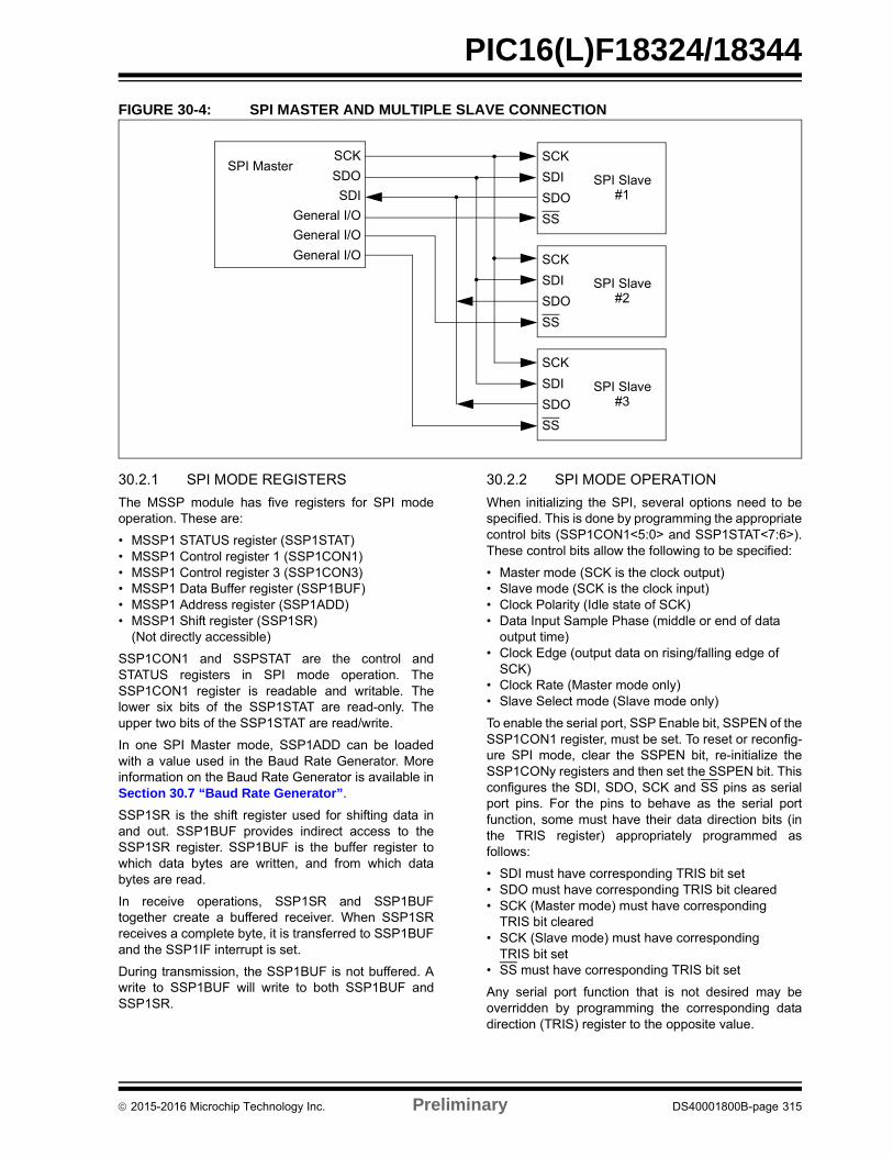
PIC16(L)F18324/18344
FIGURE 30-4: SPI MASTER AND MULTIPLE SLAVE CONNECTION
30.2.1 SPI MODE REGISTERS
The MSSP module has five registers for SPI modeoperation. These are:
• MSSP1 STATUS register (SSP1STAT)• MSSP1 Control register 1 (SSP1CON1)• MSSP1 Control register 3 (SSP1CON3)• MSSP1 Data Buffer register (SSP1BUF)• MSSP1 Address register (SSP1ADD)• MSSP1 Shift register (SSP1SR)
(Not directly accessible)
SSP1CON1 and SSPSTAT are the control andSTATUS registers in SPI mode operation. TheSSP1CON1 register is readable and writable. Thelower six bits of the SSP1STAT are read-only. Theupper two bits of the SSP1STAT are read/write.
In one SPI Master mode, SSP1ADD can be loadedwith a value used in the Baud Rate Generator. Moreinformation on the Baud Rate Generator is available inSection 30.7 “Baud Rate Generator”.
SSP1SR is the shift register used for shifting data inand out. SSP1BUF provides indirect access to theSSP1SR register. SSP1BUF is the buffer register towhich data bytes are written, and from which databytes are read.
In receive operations, SSP1SR and SSP1BUFtogether create a buffered receiver. When SSP1SRreceives a complete byte, it is transferred to SSP1BUFand the SSP1IF interrupt is set.
During transmission, the SSP1BUF is not buffered. Awrite to SSP1BUF will write to both SSP1BUF andSSP1SR.
30.2.2 SPI MODE OPERATION
When initializing the SPI, several options need to bespecified. This is done by programming the appropriatecontrol bits (SSP1CON1<5:0> and SSP1STAT<7:6>).These control bits allow the following to be specified:
• Master mode (SCK is the clock output)• Slave mode (SCK is the clock input)• Clock Polarity (Idle state of SCK)• Data Input Sample Phase (middle or end of data
output time)• Clock Edge (output data on rising/falling edge of
SCK)• Clock Rate (Master mode only)• Slave Select mode (Slave mode only)
To enable the serial port, SSP Enable bit, SSPEN of theSSP1CON1 register, must be set. To reset or reconfig-ure SPI mode, clear the SSPEN bit, re-initialize theSSP1CONy registers and then set the SSPEN bit. Thisconfigures the SDI, SDO, SCK and SS pins as serialport pins. For the pins to behave as the serial portfunction, some must have their data direction bits (inthe TRIS register) appropriately programmed asfollows:
• SDI must have corresponding TRIS bit set • SDO must have corresponding TRIS bit cleared• SCK (Master mode) must have corresponding
TRIS bit cleared• SCK (Slave mode) must have corresponding
TRIS bit set • SS must have corresponding TRIS bit set
Any serial port function that is not desired may beoverridden by programming the corresponding datadirection (TRIS) register to the opposite value.
SPI MasterSCK
SDO
SDI
General I/O
General I/O
General I/O
SCK
SDI
SDO
SS
SPI Slave#1
SCK
SDI
SDO
SS
SPI Slave#2
SCK
SDI
SDO
SS
SPI Slave#3
2015-2016 Microchip Technology Inc. Preliminary DS40001800B-page 315
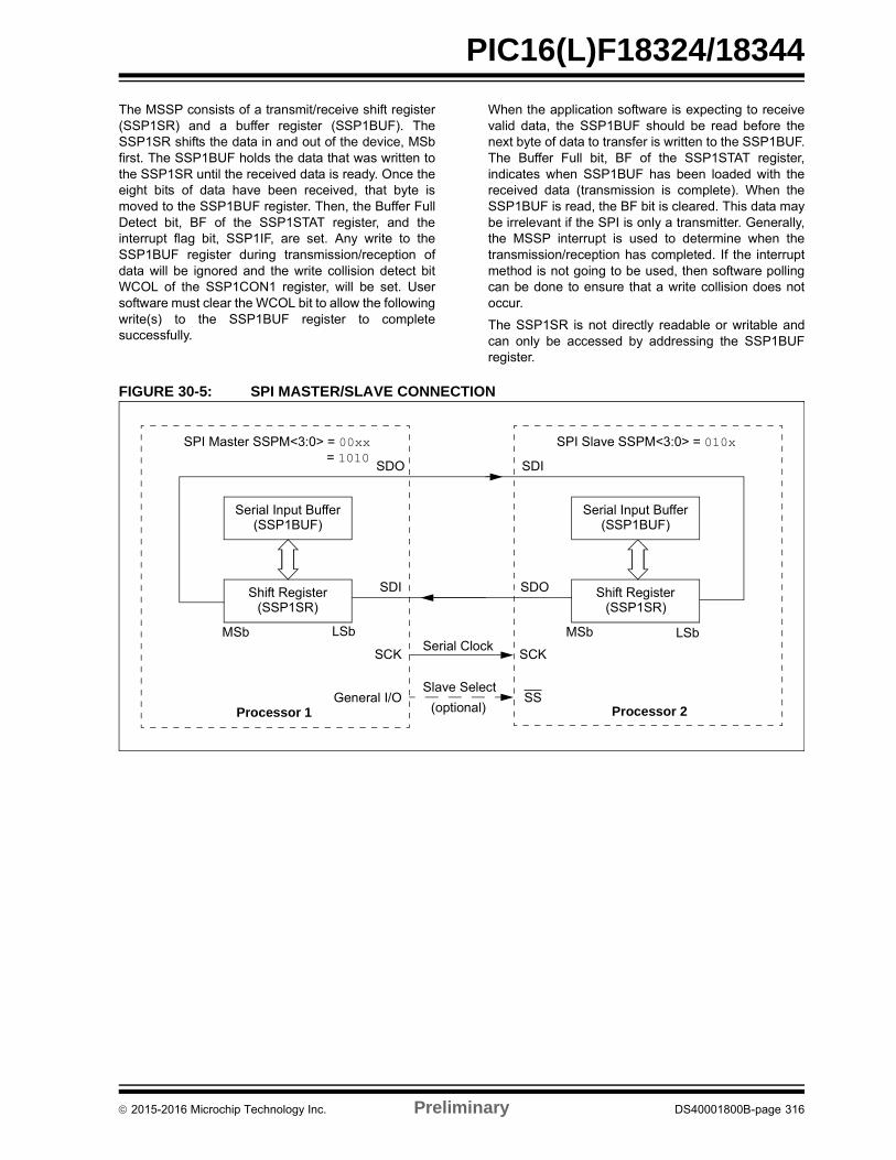
PIC16(L)F18324/18344
The MSSP consists of a transmit/receive shift register(SSP1SR) and a buffer register (SSP1BUF). TheSSP1SR shifts the data in and out of the device, MSbfirst. The SSP1BUF holds the data that was written tothe SSP1SR until the received data is ready. Once theeight bits of data have been received, that byte ismoved to the SSP1BUF register. Then, the Buffer FullDetect bit, BF of the SSP1STAT register, and theinterrupt flag bit, SSP1IF, are set. Any write to theSSP1BUF register during transmission/reception ofdata will be ignored and the write collision detect bitWCOL of the SSP1CON1 register, will be set. Usersoftware must clear the WCOL bit to allow the followingwrite(s) to the SSP1BUF register to completesuccessfully.
When the application software is expecting to receivevalid data, the SSP1BUF should be read before thenext byte of data to transfer is written to the SSP1BUF.The Buffer Full bit, BF of the SSP1STAT register,indicates when SSP1BUF has been loaded with thereceived data (transmission is complete). When theSSP1BUF is read, the BF bit is cleared. This data maybe irrelevant if the SPI is only a transmitter. Generally,the MSSP interrupt is used to determine when thetransmission/reception has completed. If the interruptmethod is not going to be used, then software pollingcan be done to ensure that a write collision does notoccur.
The SSP1SR is not directly readable or writable andcan only be accessed by addressing the SSP1BUFregister.
FIGURE 30-5: SPI MASTER/SLAVE CONNECTION
Serial Input Buffer(SSP1BUF)
Shift Register(SSP1SR)
MSb LSb
SDO
SDI
Processor 1
SCK
SPI Master SSPM<3:0> = 00xx
Serial Input Buffer(SSP1BUF)
Shift Register(SSP1SR)
LSbMSb
SDI
SDO
Processor 2
SCK
SPI Slave SSPM<3:0> = 010x
Serial Clock
SSSlave Select
General I/O(optional)
= 1010
2015-2016 Microchip Technology Inc. Preliminary DS40001800B-page 316
PIC16(L)F18324/18344
30.2.3 SPI MASTER MODE
The master can initiate the data transfer at any timebecause it controls the SCK line. The masterdetermines when the slave (Processor 2, Figure 30-5)is to broadcast data by the software protocol.
In Master mode, the data is transmitted/received assoon as the SSP1BUF register is written to. If the SPIis only going to receive, the SDO output could bedisabled (programmed as an input). The SSP1SRregister will continue to shift in the signal present on theSDI pin at the programmed clock rate. As each byte isreceived, it will be loaded into the SSP1BUF register asif a normal received byte (interrupts and Status bitsappropriately set).
The clock polarity is selected by appropriatelyprogramming the CKP bit of the SSP1CON1 registerand the CKE bit of the SSP1STAT register. This then,would give waveforms for SPI communication asshown in Figure 30-6, Figure 30-8, Figure 30-9 andFigure 30-10, where the MSB is transmitted first. InMaster mode, the SPI clock rate (bit rate) is userprogrammable to be one of the following:
• FOSC/4 (or TCY)• FOSC/16 (or 4 * TCY)• FOSC/64 (or 16 * TCY)• Timer2 output/2 • FOSC/(4 * (SSPADD + 1))
Figure 30-6 shows the waveforms for Master mode.
When the CKE bit is set, the SDO data is valid beforethere is a clock edge on SCK. The change of the inputsample is shown based on the state of the SMP bit. Thetime when the SSP1BUF is loaded with the receiveddata is shown.
FIGURE 30-6: SPI MODE WAVEFORM (MASTER MODE)
SCK(CKP = 0
SCK(CKP = 1
SCK(CKP = 0
SCK(CKP = 1
4 ClockModes
InputSample
InputSample
SDI
bit 7 bit 0
SDO bit 7 bit 6 bit 5 bit 4 bit 3 bit 2 bit 1 bit 0
bit 7
SDI
SSP1IF
(SMP = 1)
(SMP = 0)
(SMP = 1)
CKE = 1)
CKE = 0)
CKE = 1)
CKE = 0)
(SMP = 0)
Write toSSPBUF
SSP1SR toSSP1BUF
SDO bit 7 bit 6 bit 5 bit 4 bit 3 bit 2 bit 1 bit 0
(CKE = 0)
(CKE = 1)
bit 0
2015-2016 Microchip Technology Inc. Preliminary DS40001800B-page 317
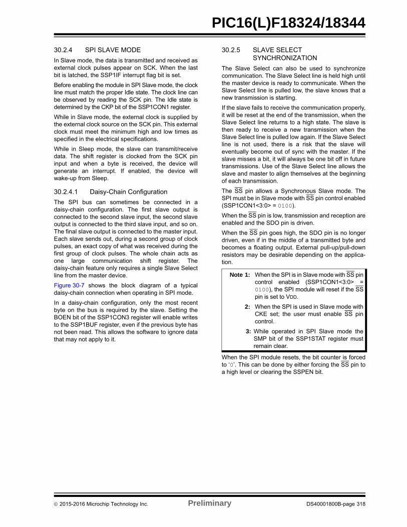
PIC16(L)F18324/18344
30.2.4 SPI SLAVE MODE
In Slave mode, the data is transmitted and received asexternal clock pulses appear on SCK. When the lastbit is latched, the SSP1IF interrupt flag bit is set.
Before enabling the module in SPI Slave mode, the clockline must match the proper Idle state. The clock line canbe observed by reading the SCK pin. The Idle state isdetermined by the CKP bit of the SSP1CON1 register.
While in Slave mode, the external clock is supplied bythe external clock source on the SCK pin. This externalclock must meet the minimum high and low times asspecified in the electrical specifications.
While in Sleep mode, the slave can transmit/receivedata. The shift register is clocked from the SCK pininput and when a byte is received, the device willgenerate an interrupt. If enabled, the device willwake-up from Sleep.
30.2.4.1 Daisy-Chain Configuration
The SPI bus can sometimes be connected in adaisy-chain configuration. The first slave output isconnected to the second slave input, the second slaveoutput is connected to the third slave input, and so on.The final slave output is connected to the master input.Each slave sends out, during a second group of clockpulses, an exact copy of what was received during thefirst group of clock pulses. The whole chain acts asone large communication shift register. Thedaisy-chain feature only requires a single Slave Selectline from the master device.
Figure 30-7 shows the block diagram of a typicaldaisy-chain connection when operating in SPI mode.
In a daisy-chain configuration, only the most recentbyte on the bus is required by the slave. Setting theBOEN bit of the SSP1CON3 register will enable writesto the SSP1BUF register, even if the previous byte hasnot been read. This allows the software to ignore datathat may not apply to it.
30.2.5 SLAVE SELECT SYNCHRONIZATION
The Slave Select can also be used to synchronizecommunication. The Slave Select line is held high untilthe master device is ready to communicate. When theSlave Select line is pulled low, the slave knows that anew transmission is starting.
If the slave fails to receive the communication properly,it will be reset at the end of the transmission, when theSlave Select line returns to a high state. The slave isthen ready to receive a new transmission when theSlave Select line is pulled low again. If the Slave Selectline is not used, there is a risk that the slave willeventually become out of sync with the master. If theslave misses a bit, it will always be one bit off in futuretransmissions. Use of the Slave Select line allows theslave and master to align themselves at the beginningof each transmission.
The SS pin allows a Synchronous Slave mode. TheSPI must be in Slave mode with SS pin control enabled(SSP1CON1<3:0> = 0100).
When the SS pin is low, transmission and reception areenabled and the SDO pin is driven.
When the SS pin goes high, the SDO pin is no longerdriven, even if in the middle of a transmitted byte andbecomes a floating output. External pull-up/pull-downresistors may be desirable depending on the applica-tion.
When the SPI module resets, the bit counter is forcedto ‘0’. This can be done by either forcing the SS pin toa high level or clearing the SSPEN bit.
Note 1: When the SPI is in Slave mode with SS pincontrol enabled (SSP1CON1<3:0> =0100), the SPI module will reset if the SSpin is set to VDD.
2: When the SPI is used in Slave mode withCKE set; the user must enable SS pincontrol.
3: While operated in SPI Slave mode theSMP bit of the SSP1STAT register mustremain clear.
2015-2016 Microchip Technology Inc. Preliminary DS40001800B-page 318
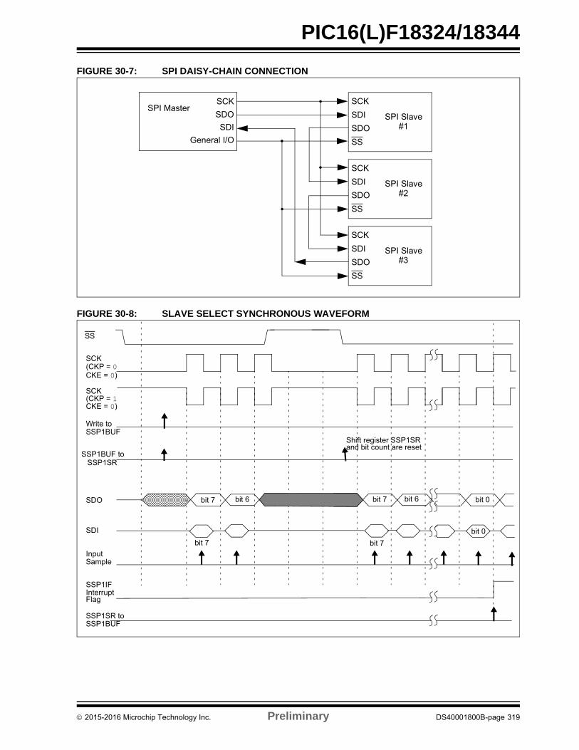
PIC16(L)F18324/18344
FIGURE 30-7: SPI DAISY-CHAIN CONNECTION
FIGURE 30-8: SLAVE SELECT SYNCHRONOUS WAVEFORM
SPI MasterSCK
SDO
SDI
General I/O
SCK
SDI
SDO
SS
SPI Slave#1
SCK
SDI
SDO
SS
SPI Slave#2
SCK
SDI
SDO
SS
SPI Slave#3
SCK(CKP = 1
SCK(CKP = 0
InputSample
SDI
bit 7
SDO bit 7 bit 6 bit 7
SSP1IFInterrupt
CKE = 0)
CKE = 0)
Write toSSP1BUF
SSP1SR toSSP1BUF
SS
Flag
bit 0
bit 7
bit 0
bit 6
SSP1BUF toSSP1SR
Shift register SSP1SRand bit count are reset
2015-2016 Microchip Technology Inc. Preliminary DS40001800B-page 319
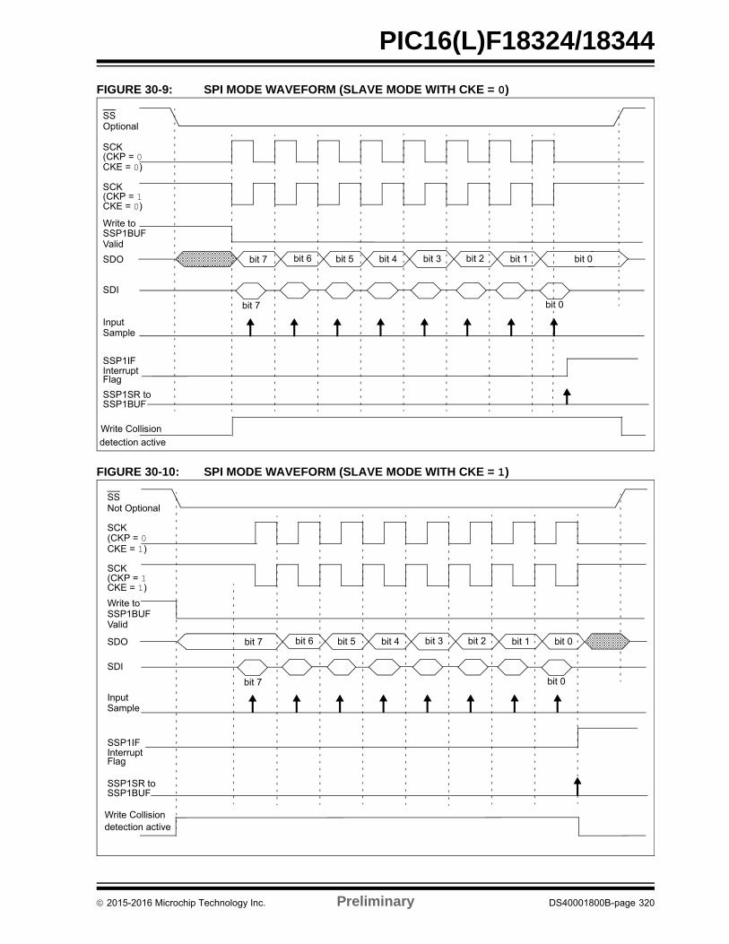
PIC16(L)F18324/18344
FIGURE 30-9: SPI MODE WAVEFORM (SLAVE MODE WITH CKE = 0)
FIGURE 30-10: SPI MODE WAVEFORM (SLAVE MODE WITH CKE = 1)
SCK(CKP = 1
SCK(CKP = 0
InputSample
SDI
bit 7
SDO bit 7 bit 6 bit 5 bit 4 bit 3 bit 2 bit 1 bit 0
SSP1IFInterrupt
CKE = 0)
CKE = 0)
Write toSSP1BUF
SSP1SR toSSP1BUF
SS
Flag
Optional
bit 0
detection active
Write Collision
Valid
SCK(CKP = 1
SCK(CKP = 0
InputSample
SDI
bit 7 bit 0
SDO bit 7 bit 6 bit 5 bit 4 bit 3 bit 2 bit 1 bit 0
SSP1IFInterrupt
CKE = 1)
CKE = 1)
Write toSSP1BUF
SSP1SR toSSP1BUF
SS
Flag
Not Optional
Write Collisiondetection active
Valid
2015-2016 Microchip Technology Inc. Preliminary DS40001800B-page 320
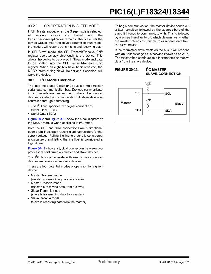
PIC16(L)F18324/18344
30.2.6 SPI OPERATION IN SLEEP MODE
In SPI Master mode, when the Sleep mode is selected,all module clocks are halted and thetransmission/reception will remain in that state until thedevice wakes. After the device returns to Run mode,the module will resume transmitting and receiving data.
In SPI Slave mode, the SPI Transmit/Receive Shiftregister operates asynchronously to the device. Thisallows the device to be placed in Sleep mode and datato be shifted into the SPI Transmit/Receive Shiftregister. When all eight bits have been received, theMSSP interrupt flag bit will be set and if enabled, willwake the device.
30.3 I2C Mode Overview
The Inter-Integrated Circuit (I2C) bus is a multi-masterserial data communication bus. Devices communicatein a master/slave environment where the masterdevices initiate the communication. A slave device iscontrolled through addressing.
• The I2C bus specifies two signal connections:• Serial Clock (SCL)• Serial Data (SDA)
Figure 30-2 and Figure 30-3 show the block diagram ofthe MSSP module when operating in I2C mode.
Both the SCL and SDA connections are bidirectionalopen-drain lines, each requiring pull-up resistors for thesupply voltage. Pulling the line to ground is considereda logical zero and letting the line float is considered alogical one.
Figure 30-11 shows a typical connection between twoprocessors configured as master and slave devices.
The I2C bus can operate with one or more masterdevices and one or more slave devices.
There are four potential modes of operation for a givendevice:
• Master Transmit mode(master is transmitting data to a slave)
• Master Receive mode(master is receiving data from a slave)
• Slave Transmit mode(slave is transmitting data to a master)
• Slave Receive mode(slave is receiving data from the master)
To begin communication, the master device sends outa Start condition followed by the address byte of theslave it intends to communicate with. This is followedby a single Read/Write bit, which determines whetherthe master intends to transmit to or receive data fromthe slave device.
If the requested slave exists on the bus, it will respondwith an Acknowledge bit, otherwise known as an ACK.The master then continues to either transmit or receivedata from the slave device.
FIGURE 30-11: I2C MASTER/SLAVE CONNECTION
Master
SCL
SDA
SCL
SDA
SlaveVDD
VDD
2015-2016 Microchip Technology Inc. Preliminary DS40001800B-page 321
PIC16(L)F18324/18344
On the last byte of data communicated, the masterdevice may end the transmission by sending a Stop bit.If the master device is in Receive mode, it sends aNACK in place of the last ACK bit. A Stop bit isindicated by a low-to-high transition of the SDA linewhile the SCL line is held high.
In some cases, the master may want to maintaincontrol of the bus and re-initiate another transmission.If so, the master device may send a Restart conditionin place of the Stop bit or last ACK bit when it is inReceive mode.
The I2C bus specifies three message protocols;
• Single message where a master writes data to a slave.
• Single message where a master reads data from a slave.
• Combined message where a master initiates a minimum of two writes, or two reads, or a combination of writes and reads, to one or more slaves.
30.3.1 CLOCK STRETCHING
When a slave device has not completed processingdata, it can delay the transfer of more data through theprocess of clock stretching. An addressed slave devicemay hold the SCL clock line low after receiving or send-ing a bit, indicating that it is not yet ready to continue.The master that is communicating with the slave willattempt to raise the SCL line in order to transfer thenext bit, but will detect that the clock line has not yetbeen released. Because the SCL connection isopen-drain, the slave has the ability to hold that line lowuntil it is ready to continue communicating.
Clock stretching allows receivers that cannot keep upwith a transmitter to control the flow of incoming data.
30.3.2 ARBITRATION
Each master device must monitor the bus for Start andStop bits. If the device detects that the bus is busy, itcannot begin a new message until the bus returns to anIdle state.
However, two master devices may try to initiate atransmission on or about the same time. When thisoccurs, the process of arbitration begins. Eachtransmitter checks the level of the SDA data line andcompares it to the level that it expects to find. The firsttransmitter to observe that the two levels do not match,loses arbitration, and must stop transmitting on theSDA line.
For example, if one transmitter holds the SDA line to alogical one (lets it float) and a second transmitter holdsit to a logical zero (pulls it low), the result is that theSDA line will be low. The first transmitter then observesthat the level of the line is different than expected andconcludes that another transmitter is communicating.
The first transmitter to notice this difference is the onethat loses arbitration and must stop driving the SDAline. If this transmitter is also a master device, it alsomust stop driving the SCL line. It then can monitor thelines for a Stop condition before trying to reissue itstransmission. In the meantime, the other device thathas not noticed any difference between the expectedand actual levels on the SDA line continues with itsoriginal transmission.
Slave Transmit mode can also be arbitrated, when amaster addresses multiple slaves, but this is lesscommon.
2015-2016 Microchip Technology Inc. Preliminary DS40001800B-page 322
PIC16(L)F18324/18344
30.4 I2C MODE OPERATION
All MSSP I2C communication is byte oriented andshifted out MSb first. Six SFR registers and twointerrupt flags interface the module with the PIC®
microcontroller and user software. Two pins, SDA andSCL, are exercised by the module to communicatewith other external I2C devices.
30.4.1 BYTE FORMAT
All communication in I2C is done in 9-bit segments. Abyte is sent from a master to a slave or vice-versa,followed by an Acknowledge bit sent back. After theeighth falling edge of the SCL line, the deviceoutputting data on the SDA changes that pin to aninput and reads in an acknowledge value on the nextclock pulse.
The clock signal, SCL, is provided by the master. Datais valid to change while the SCL signal is low, andsampled on the rising edge of the clock. Changes onthe SDA line while the SCL line is high define specialconditions on the bus, explained below.
30.4.2 DEFINITION OF I2C TERMINOLOGY
There is language and terminology in the descriptionof I2C communication that have definitions specific toI2C. That word usage is defined below and may beused in the rest of this document without explanation.This table was adapted from the Philips I2Cspecification.
30.4.3 SDA AND SCL PINS
When selecting any I2C mode, the SCL and SDA pinsshould be set by the user to inputs by setting theappropriate TRIS bits.
30.4.4 SDA HOLD TIME
The hold time of the SDA pin is selected by the SDAHTbit of the SSP1CON3 register. Hold time is the timeSDA is held valid after the falling edge of SCL. Settingthe SDAHT bit selects a longer 300 ns minimum holdtime and may help on buses with large capacitance.
Note: Any device pin can be selected for SDAand SCL functions with the PPSperipheral. These functions arebidirectional. The SDA input is selectedwith the SSPDATPPS registers. The SCLinput is selected with the SSPCLKPPSregisters. Outputs are selected with theRxyPPS registers. It is the user’sresponsibility to make the selections sothat both the input and the output for eachfunction is on the same pin.
TABLE 30-1: I2C BUS TERMS
TERM Description
Transmitter The device which shifts data out onto the bus.
Receiver The device which shifts data in from the bus.
Master The device that initiates a transfer, generates clock signals and terminates a transfer.
Slave The device addressed by the master.
Multi-master A bus with more than one device that can initiate data transfers.
Arbitration Procedure to ensure that only one master at a time controls the bus. Winning arbitration ensures that the message is not corrupted.
Synchronization Procedure to synchronize the clocks of two or more devices on the bus.
Idle No master is controlling the bus, and both SDA and SCL lines are high.
Active Any time one or more master devices are controlling the bus.
Addressed Slave
Slave device that has received a matching address and is actively being clocked by a master.
Matching Address
Address byte that is clocked into a slave that matches the value stored in SSPADD.
Write Request Slave receives a matching address with R/W bit clear, and is ready to clock in data.
Read Request Master sends an address byte with the R/W bit set, indicating that it wishes to clock data out of the Slave. This data is the next and all following bytes until a Restart or Stop.
Clock Stretching When a device on the bus hold SCL low to stall communication.
Bus Collision Any time the SDA line is sampled low by the module while it is outputting and expected high state.
2015-2016 Microchip Technology Inc. Preliminary DS40001800B-page 323
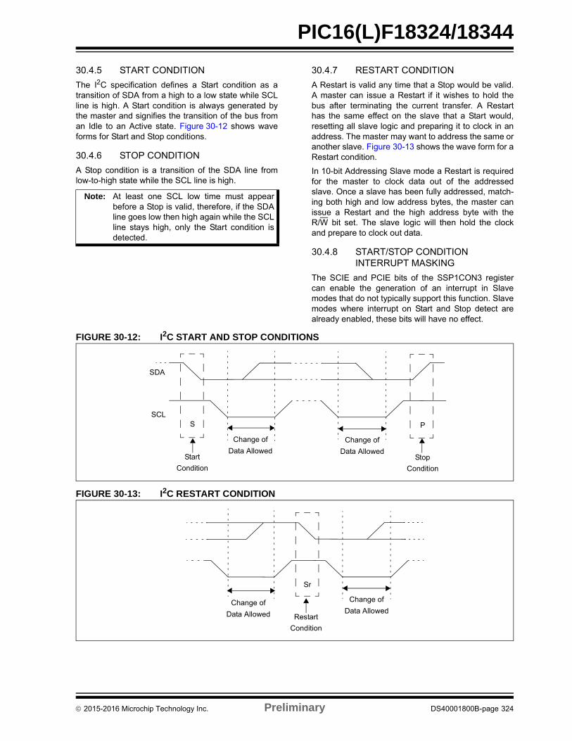
PIC16(L)F18324/18344
30.4.5 START CONDITION
The I2C specification defines a Start condition as atransition of SDA from a high to a low state while SCLline is high. A Start condition is always generated bythe master and signifies the transition of the bus froman Idle to an Active state. Figure 30-12 shows waveforms for Start and Stop conditions.
30.4.6 STOP CONDITION
A Stop condition is a transition of the SDA line fromlow-to-high state while the SCL line is high.
30.4.7 RESTART CONDITION
A Restart is valid any time that a Stop would be valid.A master can issue a Restart if it wishes to hold thebus after terminating the current transfer. A Restarthas the same effect on the slave that a Start would,resetting all slave logic and preparing it to clock in anaddress. The master may want to address the same oranother slave. Figure 30-13 shows the wave form for aRestart condition.
In 10-bit Addressing Slave mode a Restart is requiredfor the master to clock data out of the addressedslave. Once a slave has been fully addressed, match-ing both high and low address bytes, the master canissue a Restart and the high address byte with theR/W bit set. The slave logic will then hold the clockand prepare to clock out data.
30.4.8 START/STOP CONDITION INTERRUPT MASKING
The SCIE and PCIE bits of the SSP1CON3 registercan enable the generation of an interrupt in Slavemodes that do not typically support this function. Slavemodes where interrupt on Start and Stop detect arealready enabled, these bits will have no effect.
FIGURE 30-12: I2C START AND STOP CONDITIONS
FIGURE 30-13: I2C RESTART CONDITION
Note: At least one SCL low time must appearbefore a Stop is valid, therefore, if the SDAline goes low then high again while the SCLline stays high, only the Start condition isdetected.
SDA
SCL
P
Stop
Condition
S
Start
Condition
Change of
Data Allowed
Change of
Data Allowed
Restart
Condition
Sr
Change of
Data AllowedChange of
Data Allowed
2015-2016 Microchip Technology Inc. Preliminary DS40001800B-page 324
PIC16(L)F18324/18344
30.4.9 ACKNOWLEDGE SEQUENCE
The ninth SCL pulse for any transferred byte in I2C isdedicated as an Acknowledge. It allows receivingdevices to respond back to the transmitter by pullingthe SDA line low. The transmitter must release controlof the line during this time to shift in the response. TheAcknowledge (ACK) is an active-low signal, pulling theSDA line low indicates to the transmitter that thedevice has received the transmitted data and is readyto receive more.
The result of an ACK is placed in the ACKSTAT bit ofthe SSP1CON2 register.
Slave software, when the AHEN and DHEN bits areset, the clock is stretched, allowing the slave time tochange the ACK value before it is sent back to thetransmitter. The ACKDT bit of the SSP1CON2 registeris set/cleared to determine the response.
There are certain conditions where an ACK will not besent by the slave. If the BF bit of the SSP1STATregister or the SSPOV bit of the SSP1CON1 registerare set when a byte is received.
When the module is addressed, after the eighth fallingedge of SCL on the bus, the ACKTIM bit of theSSP1CON3 register is set. The ACKTIM bit indicatesthe acknowledge time of the active bus. The ACKTIMStatus bit is only active when the AHEN bit or DHENbit is enabled.
30.5 I2C SLAVE MODE OPERATION
The MSSP Slave mode operates in one of four modesselected by the SSPM bits of SSP1CON1 register. Themodes can be divided into 7-bit and 10-bit Addressingmode. 10-bit Addressing modes operate the same as7-bit with some additional overhead for handling thelarger addresses.
Modes with Start and Stop bit interrupts operate thesame as the other modes with SSP1IF additionallygetting set upon detection of a Start, Restart, or Stopcondition.
30.5.1 SLAVE MODE ADDRESSES
The SSP1ADD register (Register 30-6) contains theSlave mode address. The first byte received after aStart or Restart condition is compared against thevalue stored in this register. If the byte matches, thevalue is loaded into the SSP1BUF register and aninterrupt is generated. If the value does not match, themodule goes idle and no indication is given to thesoftware that anything happened.
The SSP Mask register (Register 30-5) affects theaddress matching process. See Section 30.5.9 “SSPMask Register” for more information.
30.5.1.1 I2C Slave 7-Bit Addressing Mode
In 7-bit Addressing mode, the LSb of the received databyte is ignored when determining if there is an addressmatch.
30.5.1.2 I2C Slave 10-Bit Addressing Mode
In 10-bit Addressing mode, the first received byte iscompared to the binary value of ‘1 1 1 1 0 A9 A8 0’. A9and A8 are the two MSb’s of the 10-bit address andstored in bits 2 and 1 of the SSP1ADD register.
After the acknowledge of the high byte the UA bit is setand SCL is held low until the user updates SSP1ADDwith the low address. The low address byte is clockedin and all eight bits are compared to the low addressvalue in SSP1ADD. Even if there is not an addressmatch; SSPIF and UA are set, and SCL is held lowuntil SSP1ADD is updated to receive a high byteagain. When SSP1ADD is updated the UA bit iscleared. This ensures the module is ready to receivethe high address byte on the next communication.
A high and low address match as a write request isrequired at the start of all 10-bit addressing communi-cation. A transmission can be initiated by issuing aRestart once the slave is addressed, and clocking inthe high address with the R/W bit set. The slavehardware will then acknowledge the read request andprepare to clock out data. This is only valid for a slaveafter it has received a complete high and low addressbyte match.
2015-2016 Microchip Technology Inc. Preliminary DS40001800B-page 325
PIC16(L)F18324/18344
30.5.2 SLAVE RECEPTION
When the R/W bit of a matching received address byteis clear, the R/W bit of the SSP1STAT register iscleared. The received address is loaded into theSSP1BUF register and acknowledged.
When the Overflow condition exists for a receivedaddress, then not Acknowledge is given. An Overflowcondition is defined as either bit BF of the SSP1STATregister is set, or bit SSPOV of the SSP1CON1 registeris set. The BOEN bit of the SSP1CON3 register modi-fies this operation. For more information seeRegister 30-4.
An MSSP interrupt is generated for each transferreddata byte. Flag bit, SSP1IF, must be cleared bysoftware.
When the SEN bit of the SSP1CON2 register is set,SCL will be held low (clock stretch) following eachreceived byte. The clock must be released by settingthe CKP bit of the SSP1CON1 register.
30.5.2.1 7-Bit Addressing Reception
This section describes a standard sequence of eventsfor the MSSP module configured as an I2C slave in7-bit Addressing mode. Figure 30-14 and Figure 30-15is used as a visual reference for this description.
This is a step-by-step process of what typically mustbe done to accomplish I2C communication.
1. Start bit detected.
2. S bit of SSP1STAT is set; SSP1IF is set if inter-rupt on Start detect is enabled.
3. Matching address with R/W bit clear is received.
4. The slave pulls SDA low sending an ACK to themaster, and sets SSP1IF bit.
5. Software clears the SSP1IF bit.
6. Software reads received address fromSSP1BUF clearing the BF flag.
7. If SEN = 1; Slave software sets CKP bit torelease the SCL line.
8. The master clocks out a data byte.
9. Slave drives SDA low sending an ACK to themaster, and sets SSP1IF bit.
10. Software clears SSP1IF.
11. Software reads the received byte fromSSP1BUF clearing BF.
12. Steps 8-12 are repeated for all received bytesfrom the master.
13. Master sends Stop condition, setting P bit ofSSP1STAT, and the bus goes idle.
30.5.2.2 7-Bit Reception with AHEN and DHEN
Slave device reception with AHEN and DHEN setoperate the same as without these options with extrainterrupts and clock stretching added after the eighthfalling edge of SCL. These additional interrupts allowtime for the slave software to decide whether it wantsto ACK the receive address or data byte.
This list describes the steps that need to be taken byslave software to use these options for I2C communi-cation. Figure 30-16 displays a module using bothaddress and data holding. Figure 30-17 includes theoperation with the SEN bit of the SSP1CON2 registerset.
1. S bit of SSP1STAT is set; SSP1IF is set if inter-rupt on Start detect is enabled.
2. Matching address with R/W bit clear is clockedin. SSP1IF is set and CKP cleared after theeighth falling edge of SCL.
3. Slave clears the SSP1IF.
4. Slave can look at the ACKTIM bit of theSSP1CON3 register to determine if the SSP1IFwas after or before the ACK.
5. Slave reads the address value from SSP1BUF,clearing the BF flag.
6. Slave sets ACK value clocked out to the masterby setting ACKDT.
7. Slave releases the clock by setting CKP.
8. SSP1IF is set after an ACK, not after a NACK.
9. If SEN = 1 the slave hardware will stretch theclock after the ACK.
10. Slave clears SSP1IF.
11. SSP1IF set and CKP cleared after eighth fallingedge of SCL for a received data byte.
12. Slave looks at ACKTIM bit of SSP1CON3 todetermine the source of the interrupt.
13. Slave reads the received data from SSP1BUFclearing BF.
14. Steps 7-14 are the same for each received databyte.
15. Communication is ended by either the slavesending an ACK = 1, or the master sending aStop condition. If a Stop is sent and Interrupt onStop Detect is disabled, the slave will only knowby polling the P bit of the SSP1STAT register.
Note: SSP1IF is still set after the ninth falling edgeof SCL even if there is no clock stretchingand BF has been cleared. Only if NACK issent to master is SSPIF not set
2015-2016 Microchip Technology Inc. Preliminary DS40001800B-page 326
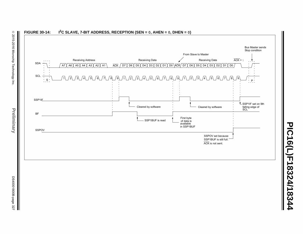
2
01
5-2
01
6 M
icroch
ip T
ech
no
log
y Inc.
Prelim
inary
DS
40
00
18
00
B-p
ag
e 3
27
PIC
16(L)F
18324/18344
FIG
ta ACK = 1
D2 D1 D0
6 7 8 9
ot sent.
set becauseF is still full.
ftwareSSP1IF set on 9thfalling edge of SCL
P
Bus Master sends Stop condition
URE 30-14: I2C SLAVE, 7-BIT ADDRESS, RECEPTION (SEN = 0, AHEN = 0, DHEN = 0)
Receiving Address
ACK
Receiving Data
ACK
Receiving Da
A7 A6 A5 A4 A3 A2 A1 D7 D6 D5 D4 D3 D2 D1 D0 D7 D6 D5 D4 D3SDA
SCL
SSP1IF
BF
SSPOV
1 2 3 4 5 6 7 8 1 2 3 4 5 6 7 8 1 2 3 4 59 9
ACK is n
SSPOV SSP1BU
Cleared by so
First byte of data is available in SSP1BUF
SSP1BUF is read
Cleared by software
S
From Slave to Master
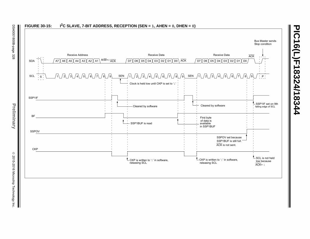
PIC
16(L)F
18324/18344
DS
40
00
18
00
B-p
ag
e 3
28
Prelim
inary
2
01
5-2
01
6 M
icroch
ip T
ech
no
log
y Inc.
5 D4 D3 D2 D1 D0
3 4 5 6 7 8 9 P
SSP1IF set on 9th
SCL is not heldtten to ‘1’ in software, low because
falling edge of SCL
SCL
ACK is not sent.
Bus Master sends
SSPOV set becauseSSP1BUF is still full.
y software
UF
ACK= 1
Stop condition
ACKReceive Data
FIGURE 30-15: I2C SLAVE, 7-BIT ADDRESS, RECEPTION (SEN = 1, AHEN = 0, DHEN = 0)
SEN SEN
A7 A6 A5 A4 A3 A2 A1 D7 D6 D5 D4 D3 D2 D1 D0 D7 D6 DSDA
SCL 1 2 3 4 5 6 7 8 9 1 2 3 4 5 6 7 8 9 1 2
CKP is wriCKP is written to ‘1’ in software,
ACK
releasing
CKP
SSPOV
BF
SSP1IF
Cleared b
First byte of data is available in SSP1B
Cleared by software
SSP1BUF is read
Clock is held low until CKP is set to ‘1’
releasing SCL
S
ACK
Receive Address Receive Data
R/W=0
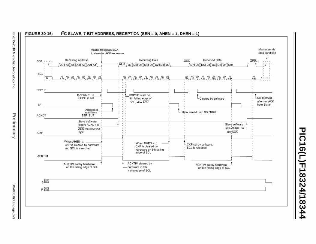
2
01
5-2
01
6 M
icroch
ip T
ech
no
log
y Inc.
Prelim
inary
DS
40
00
18
00
B-p
ag
e 3
29
PIC
16(L)F
18324/18344
FIG
P
D1 D0
7 8
Master sendsStop condition
e
Slave software
9
sets ACKDT tonot ACK
ref SCL
No interruptafter not ACKfrom Slave
ACK=1
URE 30-16: I2C SLAVE, 7-BIT ADDRESS, RECEPTION (SEN = 0, AHEN = 1, DHEN = 1)
Receiving Address Receiving Data Received Data
A7 A6 A5 A4 A3 A2 A1 D7 D6 D5 D4 D3 D2 D1 D0 D7 D6 D5 D4 D3 D2SDA
SCL
BF
CKP
S
P
1 2 3 4 5 6 7 8 9 1 2 3 4 5 6 7 8 9 1 2 3 4 5 6S
Data is read from SSP1BUF
Cleared by softwarSSP1IF is set on 9th falling edge of SCL, after ACK
CKP set by software, SCL is released
ACKTIM cleared byhardware in 9th rising edge of SCL
When DHEN = 1:CKP is cleared byhardware on 8th fallingedge of SCL
Slave softwareclears ACKDT to
ACK the receivedbyte
ACKTIM set by hardwareon 8th falling edge of SCL
When AHEN=1:CKP is cleared by hardwareand SCL is stretched
Address isread from
SSP1BUF
ACKTIM set by hardwaon 8th falling edge o
ACK
Master Releases SDAto slave for ACK sequence
ACK
ACKDT
ACKTIM
SSP1IF
If AHEN = 1:SSPIF is set
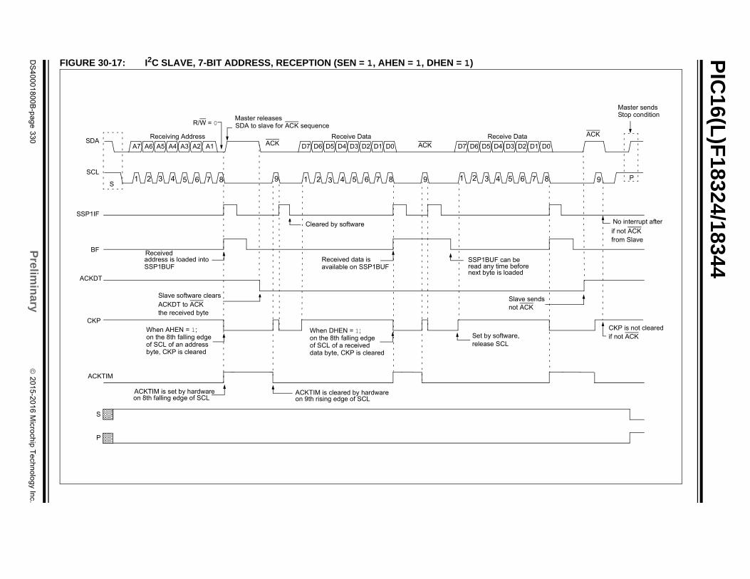
PIC
16(L)F
18324/18344
DS
40
00
18
00
B-p
ag
e 3
30
Prelim
inary
2
01
5-2
01
6 M
icroch
ip T
ech
no
log
y Inc.
Data
D2 D1 D0
6 7 8 9
ACK
be
re,
eforeded
lave sendsot ACK
CKP is not clearedif not ACK
P
Master sendsStop condition
No interrupt after
if not ACKfrom Slave
FIGURE 30-17: I2C SLAVE, 7-BIT ADDRESS, RECEPTION (SEN = 1, AHEN = 1, DHEN = 1)
Receiving Address Receive Data Receive
A7 A6 A5 A4 A3 A2 A1 D7 D6 D5 D4 D3 D2 D1 D0 D7 D6 D5 D4 D3SDA
SCL
SSP1IF
BF
ACKDT
CKP
S
P
ACK
S1 2 3 4 5 6 7 8 9 1 2 3 4 5 6 7 8 9 1 2 3 4 5
ACK
Cleared by software
ACKTIM is cleared by hardware
SSP1BUF can
Set by softwa
read any time bnext byte is loa
release SCL
on 9th rising edge of SCL
Received address is loaded into SSP1BUF
Slave software clearsACKDT to ACK
R/W = 0Master releasesSDA to slave for ACK sequence
the received byte
When AHEN = 1;on the 8th falling edgeof SCL of an addressbyte, CKP is cleared
ACKTIM is set by hardwareon 8th falling edge of SCL
When DHEN = 1;on the 8th falling edgeof SCL of a receiveddata byte, CKP is cleared
Received data isavailable on SSP1BUF
Sn
ACKTIM
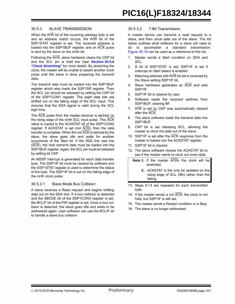
PIC16(L)F18324/18344
30.5.3 SLAVE TRANSMISSION
When the R/W bit of the incoming address byte is setand an address match occurs, the R/W bit of theSSP1STAT register is set. The received address isloaded into the SSP1BUF register, and an ACK pulseis sent by the slave on the ninth bit.
Following the ACK, slave hardware clears the CKP bitand the SCL pin is held low (see Section 30.5.6“Clock Stretching” for more detail). By stretching theclock, the master will be unable to assert another clockpulse until the slave is done preparing the transmitdata.
The transmit data must be loaded into the SSP1BUFregister which also loads the SSP1SR register. Thenthe SCL pin should be released by setting the CKP bitof the SSP1CON1 register. The eight data bits areshifted out on the falling edge of the SCL input. Thisensures that the SDA signal is valid during the SCLhigh time.
The ACK pulse from the master-receiver is latched onthe rising edge of the ninth SCL input pulse. This ACKvalue is copied to the ACKSTAT bit of the SSP1CON2register. If ACKSTAT is set (not ACK), then the datatransfer is complete. When the not ACK is latched by theslave, the slave goes idle and waits for anotheroccurrence of the Start bit. If the SDA line was low(ACK), the next transmit data must be loaded into theSSP1BUF register. Again, the SCL pin must be releasedby setting bit CKP.
An MSSP interrupt is generated for each data transferbyte. The SSP1IF bit must be cleared by software andthe SSP1STAT register is used to determine the statusof the byte. The SSP1IF bit is set on the falling edge ofthe ninth clock pulse.
30.5.3.1 Slave Mode Bus Collision
A slave receives a Read request and begins shiftingdata out on the SDA line. If a bus collision is detectedand the SBCDE bit of the SSP1CON3 register is set,the BCLIF bit of the PIR register is set. Once a bus col-lision is detected, the slave goes idle and waits to beaddressed again. User software can use the BCLIF bitto handle a slave bus collision.
30.5.3.2 7-Bit Transmission
A master device can transmit a read request to aslave, and then clock data out of the slave. The listbelow outlines what software for a slave will need todo to accomplish a standard transmission.Figure 30-18 can be used as a reference to this list.
1. Master sends a Start condition on SDA andSCL.
2. S bit of SSP1STAT is set; SSP1IF is set ifinterrupt on Start detect is enabled.
3. Matching address with R/W bit set is received bythe Slave setting SSP1IF bit.
4. Slave hardware generates an ACK and setsSSP1IF.
5. SSP1IF bit is cleared by user.
6. Software reads the received address fromSSP1BUF, clearing BF.
7. R/W is set so CKP was automatically clearedafter the ACK.
8. The slave software loads the transmit data intoSSP1BUF.
9. CKP bit is set releasing SCL, allowing themaster to clock the data out of the slave.
10. SSP1IF is set after the ACK response from themaster is loaded into the ACKSTAT register.
11. SSP1IF bit is cleared.
12. The slave software checks the ACKSTAT bit tosee if the master wants to clock out more data.
13. Steps 9-13 are repeated for each transmittedbyte.
14. If the master sends a not ACK; the clock is notheld, but SSP1IF is still set.
15. The master sends a Restart condition or a Stop.
16. The slave is no longer addressed.
Note 1: If the master ACKs the clock will bestretched.
2: ACKSTAT is the only bit updated on therising edge of SCL (9th) rather than thefalling.
2015-2016 Microchip Technology Inc. Preliminary DS40001800B-page 331
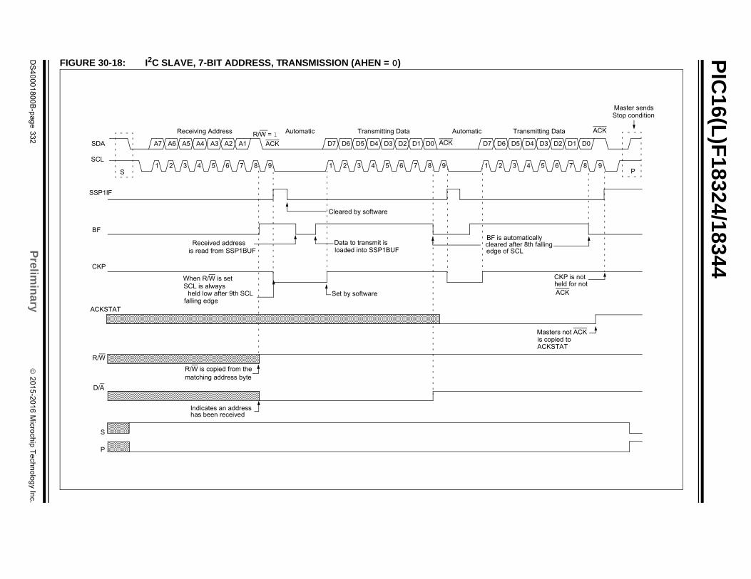
PIC
16(L)F
18324/18344
DS
40
00
18
00
B-p
ag
e 3
32
Prelim
inary
2
01
5-2
01
6 M
icroch
ip T
ech
no
log
y Inc.
Transmitting Data
5 D4 D3 D2 D1 D0
3 4 5 6 7 8 9
Masters not ACKis copied to ACKSTAT
CKP is not held for not ACK
omatically fter 8th fallingCL
ACK
P
Master sendsStop condition
FIGURE 30-18: I2C SLAVE, 7-BIT ADDRESS, TRANSMISSION (AHEN = 0)
Receiving Address Automatic Transmitting Data Automatic
A7 A6 A5 A4 A3 A2 A1 D7 D6 D5 D4 D3 D2 D1 D0 D7 D6 D
1 2 3 4 5 6 7 8 9 1 2 3 4 5 6 7 8 9 1 2
SDA
SCL
SSP1IF
BF
CKP
ACKSTAT
R/W
D/A
S
P
Received address
When R/W is set
R/W is copied from the
Indicates an address
is read from SSP1BUF
SCL is alwaysheld low after 9th SCL
falling edge
matching address byte
has been received
BF is autcleared aedge of S
Data to transmit isloaded into SSP1BUF
Set by software
Cleared by software
ACKACK
R/W = 1
S
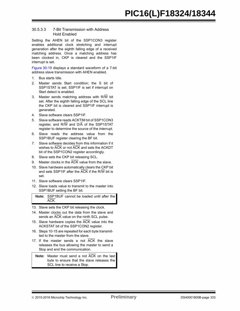
PIC16(L)F18324/18344
30.5.3.3 7-Bit Transmission with Address Hold Enabled
Setting the AHEN bit of the SSP1CON3 registerenables additional clock stretching and interruptgeneration after the eighth falling edge of a receivedmatching address. Once a matching address hasbeen clocked in, CKP is cleared and the SSP1IFinterrupt is set.
Figure 30-19 displays a standard waveform of a 7-bitaddress slave transmission with AHEN enabled.
1. Bus starts Idle.
2. Master sends Start condition; the S bit ofSSP1STAT is set; SSP1IF is set if interrupt onStart detect is enabled.
3. Master sends matching address with R/W bitset. After the eighth falling edge of the SCL linethe CKP bit is cleared and SSP1IF interrupt isgenerated.
4. Slave software clears SSP1IF.
5. Slave software reads ACKTIM bit of SSP1CON3register, and R/W and D/A of the SSP1STATregister to determine the source of the interrupt.
6. Slave reads the address value from theSSP1BUF register clearing the BF bit.
7. Slave software decides from this information if itwishes to ACK or not ACK and sets the ACKDTbit of the SSP1CON2 register accordingly.
8. Slave sets the CKP bit releasing SCL.
9. Master clocks in the ACK value from the slave.
10. Slave hardware automatically clears the CKP bitand sets SSP1IF after the ACK if the R/W bit isset.
11. Slave software clears SSP1IF.
12. Slave loads value to transmit to the master intoSSP1BUF setting the BF bit.
13. Slave sets the CKP bit releasing the clock.
14. Master clocks out the data from the slave andsends an ACK value on the ninth SCL pulse.
15. Slave hardware copies the ACK value into theACKSTAT bit of the SSP1CON2 register.
16. Steps 10-15 are repeated for each byte transmit-ted to the master from the slave.
17. If the master sends a not ACK the slavereleases the bus allowing the master to send aStop and end the communication.
Note: SSP1BUF cannot be loaded until after theACK.
Note: Master must send a not ACK on the lastbyte to ensure that the slave releases theSCL line to receive a Stop.
2015-2016 Microchip Technology Inc. Preliminary DS40001800B-page 333
PIC
16(L)F
18324/18344
DS
40
00
18
00
B-p
ag
e 3
34
Prelim
inary
2
01
5-2
01
6 M
icroch
ip T
ech
no
log
y Inc.
Transmitting Data
6 D5 D4 D3 D2 D1 D0
3 4 5 6 7 8 9
BF is automatically cleared after 8th fallingedge of SCL
Master’s ACKresponse is copied
to SSP1STAT
CKP not cleared
after not ACK
P
Master sendsStop condition
ACK
FIGURE 30-19: I2C SLAVE, 7-BIT ADDRESS, TRANSMISSION (AHEN = 1)
Receiving Address Automatic Transmitting Data Automatic
A7 A6 A5 A4 A3 A2 A1 D7 D6 D5 D4 D3 D2 D1 D0 D7 D
1 2 3 4 5 6 7 8 9 1 2 3 4 5 6 7 8 9 1 2
SDA
SCL
SSP1IF
BF
ACKDT
ACKSTAT
CKP
R/W
D/A
Received address
is read from SSP1BUFData to transmit isloaded into SSP1BUF
Cleared by software
Slave clears
ACKDT to ACKaddress
Set by software,releases SCL
ACKTIM is clearedon 9th rising edge of SCL
ACKTIM is set on 8th fallingedge of SCL
When AHEN = 1;CKP is cleared by hardwareafter receiving matchingaddress.
When R/W = 1;CKP is alwayscleared after ACK
S
ACKR/W = 1
Master releases SDAto slave for ACK sequence
ACK
ACKTIM
PIC16(L)F18324/18344
30.5.4 SLAVE MODE 10-BIT ADDRESS RECEPTION
This section describes a standard sequence of eventsfor the MSSP module configured as an I2C slave in10-bit Addressing mode.
Figure 30-20 is used as a visual reference for thisdescription.
This is a step-by-step process of what must be doneby slave software to accomplish I2C communication.
1. Bus starts Idle.
2. Master sends Start condition; S bit ofSSP1STAT is set; SSP1IF is set if interrupt onStart detect is enabled.
3. Master sends matching high address with R/Wbit clear; UA bit of the SSP1STAT register is set.
4. Slave sends ACK and SSP1IF is set.
5. Software clears the SSP1IF bit.
6. Software reads received address fromSSP1BUF clearing the BF flag.
7. Slave loads low address into SSP1ADD,releasing SCL.
8. Master sends matching low address byte to theslave; UA bit is set.
9. Slave sends ACK and SSP1IF is set.
10. Slave clears SSP1IF.
11. Slave reads the received matching addressfrom SSP1BUF clearing BF.
12. Slave loads high address into SSP1ADD.
13. Master clocks a data byte to the slave andclocks out the slaves ACK on the ninth SCLpulse; SSP1IF is set.
14. If SEN bit of SSP1CON2 is set, CKP is clearedby hardware and the clock is stretched.
15. Slave clears SSP1IF.
16. Slave reads the received byte from SSP1BUFclearing BF.
17. If SEN is set the slave sets CKP to release theSCL.
18. Steps 13-17 repeat for each received byte.
19. Master sends Stop to end the transmission.
30.5.5 10-BIT ADDRESSING WITH ADDRESS OR DATA HOLD
Reception using 10-bit addressing with AHEN orDHEN set is the same as with 7-bit modes. The onlydifference is the need to update the SSP1ADD registerusing the UA bit. All functionality, specifically when theCKP bit is cleared and SCL line is held low are thesame. Figure 30-21 can be used as a reference of aslave in 10-bit addressing with AHEN set.
Figure 30-22 shows a standard waveform for a slavetransmitter in 10-bit Addressing mode.
Note: Updates to the SSP1ADD register are notallowed until after the ACK sequence.
Note: If the low address does not match, SSP1IFand UA are still set so that the slavesoftware can set SSP1ADD back to the highaddress. BF is not set because there is nomatch. CKP is unaffected.
2015-2016 Microchip Technology Inc. Preliminary DS40001800B-page 335
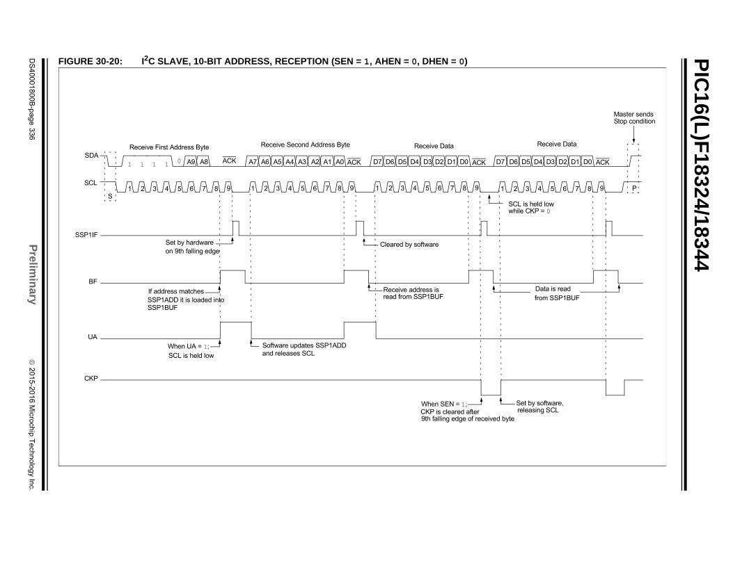
PIC
16(L)F
18324/18344
DS
40
00
18
00
B-p
ag
e 3
36
Prelim
inary
2
01
5-2
01
6 M
icroch
ip T
ech
no
log
y Inc.
Receive Data
ACK7 D6 D5 D4 D3 D2 D1 D0
1 2 3 4 5 6 7 8 9 P
Master sendsStop condition
Data is read
SCL is held low
Set by software,
while CKP = 0
from SSP1BUF
releasing SCL byte
FIGURE 30-20: I2C SLAVE, 10-BIT ADDRESS, RECEPTION (SEN = 1, AHEN = 0, DHEN = 0)
SSP1IF
Receive First Address Byte
ACK
Receive Second Address Byte
ACK
Receive Data
ACK1 1 1 1 0 A9 A8 A7 A6 A5 A4 A3 A2 A1 A0 D7 D6 D5 D4 D3 D2 D1 D0 DSDA
SCL
UA
CKP
1 2 3 4 5 6 7 8 9 1 2 3 4 5 6 7 8 9 1 2 3 4 5 6 7 8 9
Cleared by software
Receive address is
Software updates SSP1ADD
When SEN = 1;CKP is cleared after9th falling edge of received
read from SSP1BUF
and releases SCLWhen UA = 1;
If address matches
Set by hardwareon 9th falling edge
SSP1ADD it is loaded into SSP1BUF
SCL is held low
S
BF
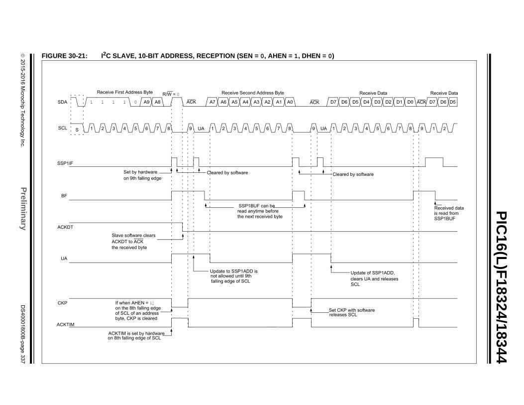
2
01
5-2
01
6 M
icroch
ip T
ech
no
log
y Inc.
Prelim
inary
DS
40
00
18
00
B-p
ag
e 3
37
PIC
16(L)F
18324/18344
FIG
ive Data
ACK
Receive Data
D3 D2 D1 D0 D7 D6 D5
5 6 7 8 9 1 2
SSP1BUFis read from Received data
re
and releasesf SSP1ADD,
re
URE 30-21: I2C SLAVE, 10-BIT ADDRESS, RECEPTION (SEN = 0, AHEN = 1, DHEN = 0)
Receive First Address Byte
UA
Receive Second Address Byte
UA
Rece
1 1 1 1 0 A9 A8 A7 A6 A5 A4 A3 A2 A1 A0 D7 D6 D5 D4SDA
SCL
SSP1IF
BF
ACKDT
UA
CKP
ACKTIM
1 2 3 4 5 6 7 8 9S
ACKACK
1 2 3 4 5 6 7 8 9 1 2 3 4
SSP1BUF can beread anytime beforethe next received byte
Cleared by software
falling edge of SCLnot allowed until 9thUpdate to SSP1ADD is
Set CKP with softwareleases SCL
SCLclears UAUpdate o
Set by hardwareon 9th falling edge
Slave software clearsACKDT to ACKthe received byte
If when AHEN = 1;on the 8th falling edgeof SCL of an addressbyte, CKP is cleared
ACKTIM is set by hardwareon 8th falling edge of SCL
Cleared by softwa
R/W = 0
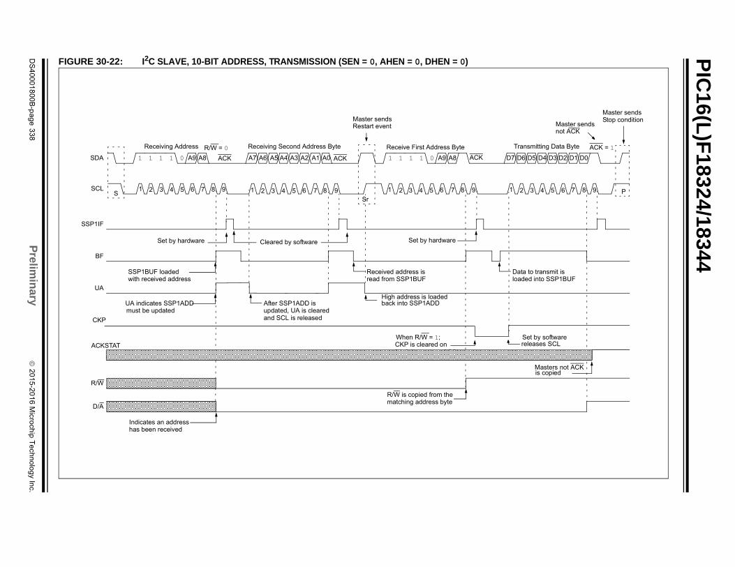
PIC
16(L)F
18324/18344
DS
40
00
18
00
B-p
ag
e 3
38
Prelim
inary
2
01
5-2
01
6 M
icroch
ip T
ech
no
log
y Inc.
Transmitting Data Byte
D7 D6 D5 D4 D3 D2 D1 D0
1 2 3 4 5 6 7 8 9
ACK = 1
P
Master sends Stop condition
Master sends not ACK
Data to transmit is
Set by software
loaded into SSP1BUF
releases SCL
Masters not ACKis copied
FIGURE 30-22: I2C SLAVE, 10-BIT ADDRESS, TRANSMISSION (SEN = 0, AHEN = 0, DHEN = 0)
Receiving Address
ACK
Receiving Second Address Byte
Sr
Receive First Address Byte
ACK1 1 1 1 0 A9 A8 A7 A6 A5 A4 A3 A2 A1 A0 1 1 1 1 0 A9 A8SDA
SCL
SSP1IF
BF
UA
CKP
R/W
D/A
1 2 3 4 5 6 7 8 9 1 2 3 4 5 6 7 8 9 1 2 3 4 5 6 7 8 9
Master sends Restart event
ACK
R/W = 0
S
Cleared by software
After SSP1ADD isupdated, UA is clearedand SCL is released
High address is loaded
Received address is
Indicates an address
When R/W = 1;
R/W is copied from the
Set by hardware
UA indicates SSP1ADD
SSP1BUF loadedwith received address
must be updated
has been received
matching address byte
CKP is cleared on9th falling edge of SCL
read from SSP1BUF
back into SSP1ADD
ACKSTAT
Set by hardware
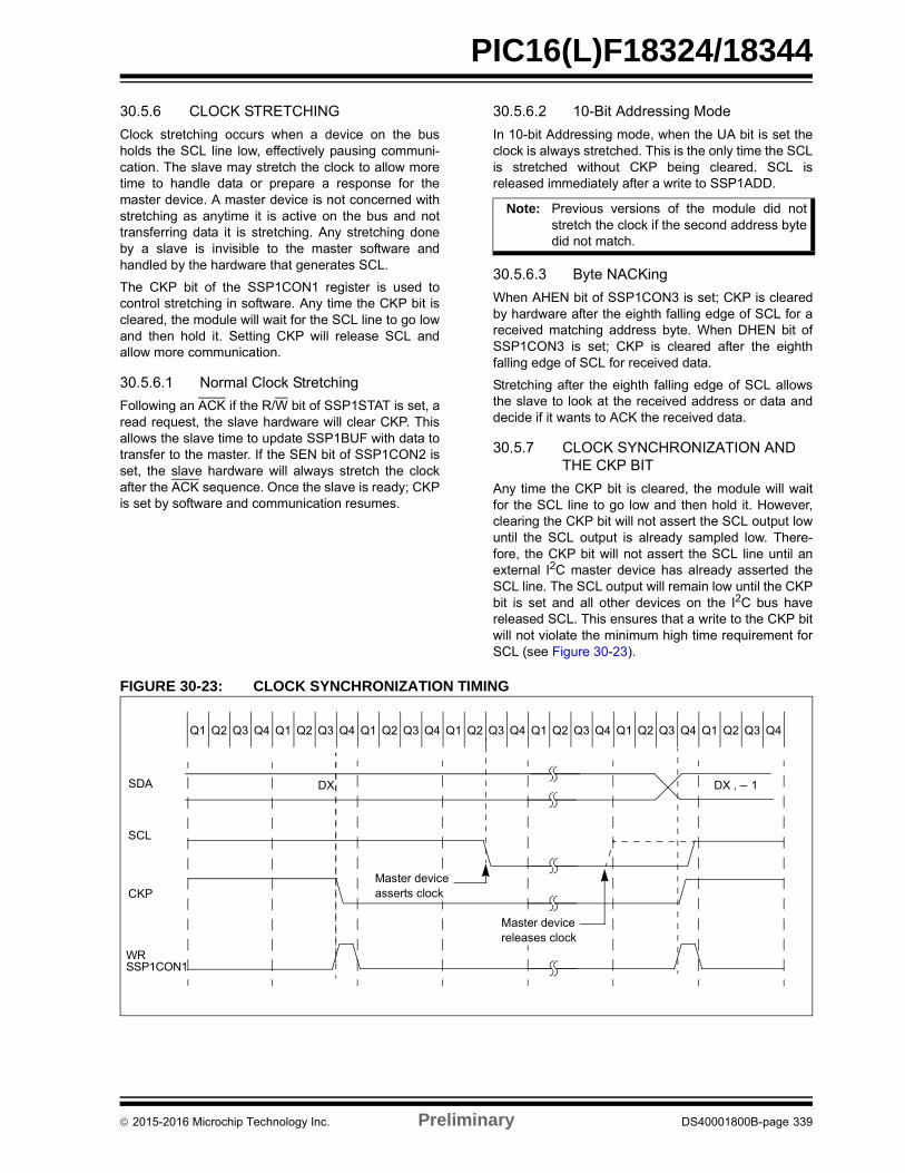
PIC16(L)F18324/18344
30.5.6 CLOCK STRETCHING
Clock stretching occurs when a device on the busholds the SCL line low, effectively pausing communi-cation. The slave may stretch the clock to allow moretime to handle data or prepare a response for themaster device. A master device is not concerned withstretching as anytime it is active on the bus and nottransferring data it is stretching. Any stretching doneby a slave is invisible to the master software andhandled by the hardware that generates SCL.
The CKP bit of the SSP1CON1 register is used tocontrol stretching in software. Any time the CKP bit iscleared, the module will wait for the SCL line to go lowand then hold it. Setting CKP will release SCL andallow more communication.
30.5.6.1 Normal Clock Stretching
Following an ACK if the R/W bit of SSP1STAT is set, aread request, the slave hardware will clear CKP. Thisallows the slave time to update SSP1BUF with data totransfer to the master. If the SEN bit of SSP1CON2 isset, the slave hardware will always stretch the clockafter the ACK sequence. Once the slave is ready; CKPis set by software and communication resumes.
30.5.6.2 10-Bit Addressing Mode
In 10-bit Addressing mode, when the UA bit is set theclock is always stretched. This is the only time the SCLis stretched without CKP being cleared. SCL isreleased immediately after a write to SSP1ADD.
30.5.6.3 Byte NACKing
When AHEN bit of SSP1CON3 is set; CKP is clearedby hardware after the eighth falling edge of SCL for areceived matching address byte. When DHEN bit ofSSP1CON3 is set; CKP is cleared after the eighthfalling edge of SCL for received data.
Stretching after the eighth falling edge of SCL allowsthe slave to look at the received address or data anddecide if it wants to ACK the received data.
30.5.7 CLOCK SYNCHRONIZATION AND THE CKP BIT
Any time the CKP bit is cleared, the module will waitfor the SCL line to go low and then hold it. However,clearing the CKP bit will not assert the SCL output lowuntil the SCL output is already sampled low. There-fore, the CKP bit will not assert the SCL line until anexternal I2C master device has already asserted theSCL line. The SCL output will remain low until the CKPbit is set and all other devices on the I2C bus havereleased SCL. This ensures that a write to the CKP bitwill not violate the minimum high time requirement forSCL (see Figure 30-23).
FIGURE 30-23: CLOCK SYNCHRONIZATION TIMING
Note: Previous versions of the module did notstretch the clock if the second address bytedid not match.
SDA
SCL
DX ‚ – 1DX
WR
Q1 Q2 Q3 Q4 Q1 Q2 Q3 Q4 Q1 Q2 Q3 Q4 Q1 Q2 Q3 Q4 Q1 Q2 Q3 Q4 Q1 Q2 Q3 Q4 Q1 Q2 Q3 Q4
SSP1CON1
CKP
Master devicereleases clock
Master deviceasserts clock
2015-2016 Microchip Technology Inc. Preliminary DS40001800B-page 339
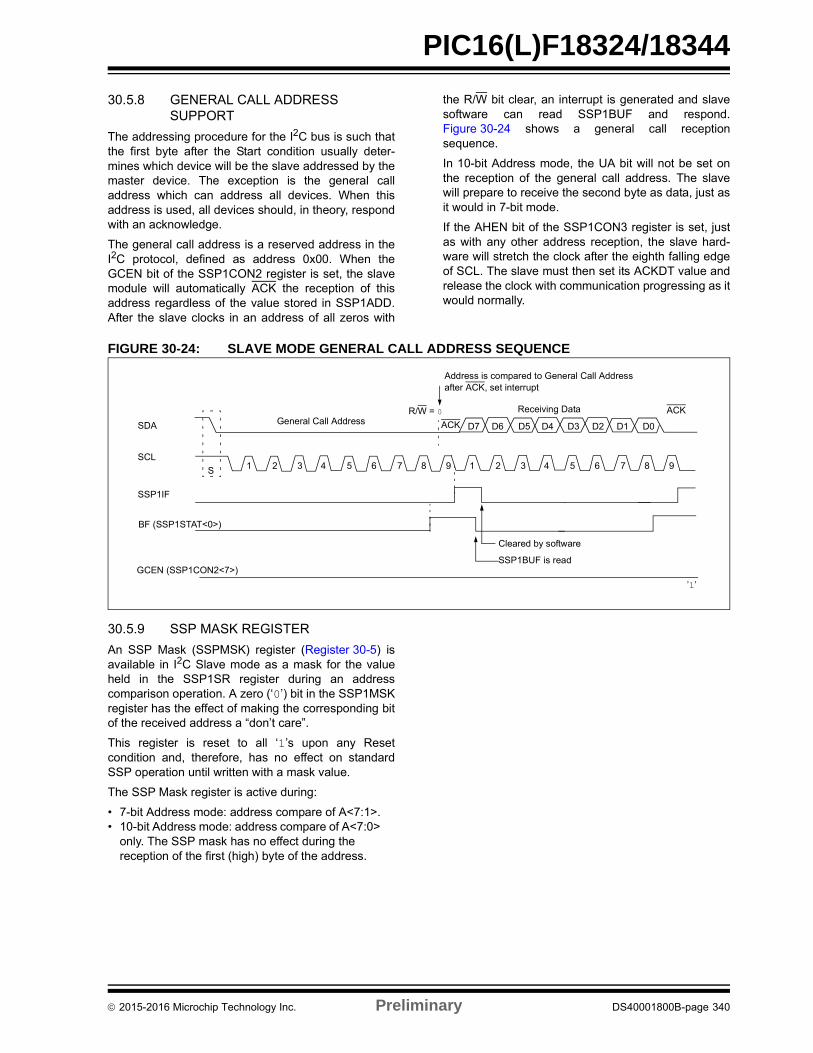
PIC16(L)F18324/18344
30.5.8 GENERAL CALL ADDRESS SUPPORT
The addressing procedure for the I2C bus is such thatthe first byte after the Start condition usually deter-mines which device will be the slave addressed by themaster device. The exception is the general calladdress which can address all devices. When thisaddress is used, all devices should, in theory, respondwith an acknowledge.
The general call address is a reserved address in theI2C protocol, defined as address 0x00. When theGCEN bit of the SSP1CON2 register is set, the slavemodule will automatically ACK the reception of thisaddress regardless of the value stored in SSP1ADD.After the slave clocks in an address of all zeros with
the R/W bit clear, an interrupt is generated and slavesoftware can read SSP1BUF and respond.Figure 30-24 shows a general call receptionsequence.
In 10-bit Address mode, the UA bit will not be set onthe reception of the general call address. The slavewill prepare to receive the second byte as data, just asit would in 7-bit mode.
If the AHEN bit of the SSP1CON3 register is set, justas with any other address reception, the slave hard-ware will stretch the clock after the eighth falling edgeof SCL. The slave must then set its ACKDT value andrelease the clock with communication progressing as itwould normally.
FIGURE 30-24: SLAVE MODE GENERAL CALL ADDRESS SEQUENCE
30.5.9 SSP MASK REGISTER
An SSP Mask (SSPMSK) register (Register 30-5) isavailable in I2C Slave mode as a mask for the valueheld in the SSP1SR register during an addresscomparison operation. A zero (‘0’) bit in the SSP1MSKregister has the effect of making the corresponding bitof the received address a “don’t care”.
This register is reset to all ‘1’s upon any Resetcondition and, therefore, has no effect on standardSSP operation until written with a mask value.
The SSP Mask register is active during:
• 7-bit Address mode: address compare of A<7:1>.• 10-bit Address mode: address compare of A<7:0>
only. The SSP mask has no effect during the reception of the first (high) byte of the address.
SDA
SCL
S
SSP1IF
BF (SSP1STAT<0>)
Cleared by software
SSP1BUF is read
R/W = 0
ACKGeneral Call Address
Address is compared to General Call Address
Receiving Data ACK
1 2 3 4 5 6 7 8 9 1 2 3 4 5 6 7 8 9
D7 D6 D5 D4 D3 D2 D1 D0
after ACK, set interrupt
GCEN (SSP1CON2<7>)
’1’
2015-2016 Microchip Technology Inc. Preliminary DS40001800B-page 340
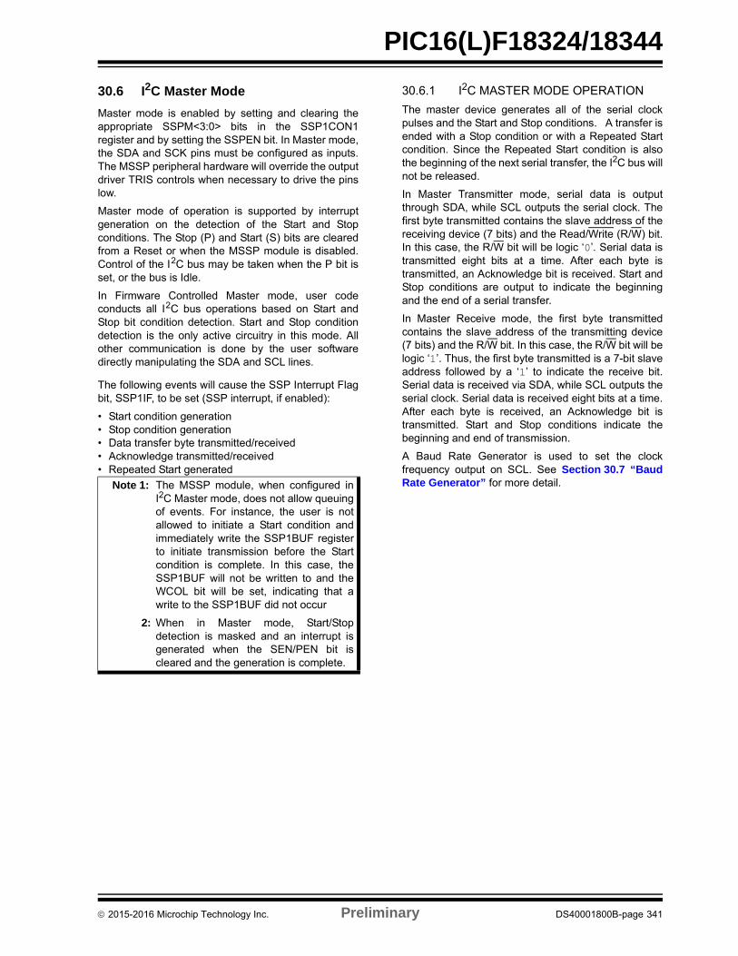
PIC16(L)F18324/18344
30.6 I2C Master Mode
Master mode is enabled by setting and clearing theappropriate SSPM<3:0> bits in the SSP1CON1register and by setting the SSPEN bit. In Master mode,the SDA and SCK pins must be configured as inputs.The MSSP peripheral hardware will override the outputdriver TRIS controls when necessary to drive the pinslow.
Master mode of operation is supported by interruptgeneration on the detection of the Start and Stopconditions. The Stop (P) and Start (S) bits are clearedfrom a Reset or when the MSSP module is disabled.Control of the I2C bus may be taken when the P bit isset, or the bus is Idle.
In Firmware Controlled Master mode, user codeconducts all I2C bus operations based on Start andStop bit condition detection. Start and Stop conditiondetection is the only active circuitry in this mode. Allother communication is done by the user softwaredirectly manipulating the SDA and SCL lines.
The following events will cause the SSP Interrupt Flagbit, SSP1IF, to be set (SSP interrupt, if enabled):
• Start condition generation• Stop condition generation• Data transfer byte transmitted/received• Acknowledge transmitted/received• Repeated Start generated
30.6.1 I2C MASTER MODE OPERATION
The master device generates all of the serial clockpulses and the Start and Stop conditions. A transfer isended with a Stop condition or with a Repeated Startcondition. Since the Repeated Start condition is alsothe beginning of the next serial transfer, the I2C bus willnot be released.
In Master Transmitter mode, serial data is outputthrough SDA, while SCL outputs the serial clock. Thefirst byte transmitted contains the slave address of thereceiving device (7 bits) and the Read/Write (R/W) bit.In this case, the R/W bit will be logic ‘0’. Serial data istransmitted eight bits at a time. After each byte istransmitted, an Acknowledge bit is received. Start andStop conditions are output to indicate the beginningand the end of a serial transfer.
In Master Receive mode, the first byte transmittedcontains the slave address of the transmitting device(7 bits) and the R/W bit. In this case, the R/W bit will belogic ‘1’. Thus, the first byte transmitted is a 7-bit slaveaddress followed by a ‘1’ to indicate the receive bit.Serial data is received via SDA, while SCL outputs theserial clock. Serial data is received eight bits at a time.After each byte is received, an Acknowledge bit istransmitted. Start and Stop conditions indicate thebeginning and end of transmission.
A Baud Rate Generator is used to set the clockfrequency output on SCL. See Section 30.7 “BaudRate Generator” for more detail.Note 1: The MSSP module, when configured in
I2C Master mode, does not allow queuingof events. For instance, the user is notallowed to initiate a Start condition andimmediately write the SSP1BUF registerto initiate transmission before the Startcondition is complete. In this case, theSSP1BUF will not be written to and theWCOL bit will be set, indicating that awrite to the SSP1BUF did not occur
2: When in Master mode, Start/Stopdetection is masked and an interrupt isgenerated when the SEN/PEN bit iscleared and the generation is complete.
2015-2016 Microchip Technology Inc. Preliminary DS40001800B-page 341
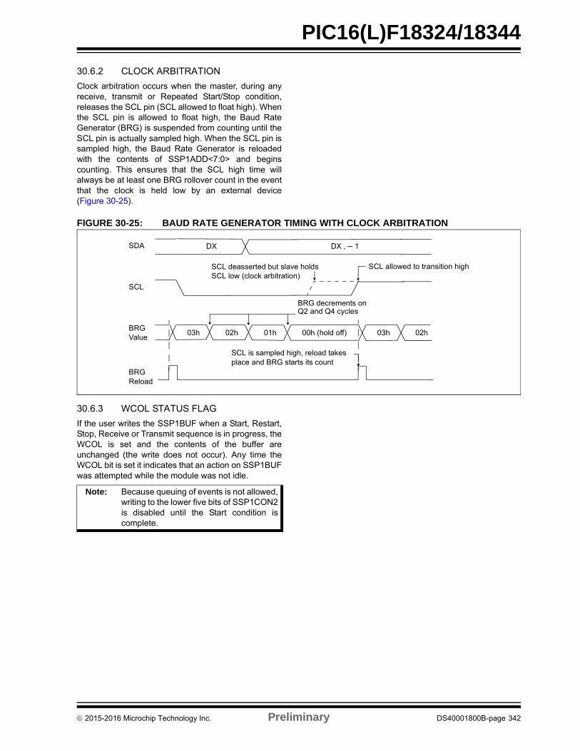
PIC16(L)F18324/18344
30.6.2 CLOCK ARBITRATION
Clock arbitration occurs when the master, during anyreceive, transmit or Repeated Start/Stop condition,releases the SCL pin (SCL allowed to float high). Whenthe SCL pin is allowed to float high, the Baud RateGenerator (BRG) is suspended from counting until theSCL pin is actually sampled high. When the SCL pin issampled high, the Baud Rate Generator is reloadedwith the contents of SSP1ADD<7:0> and beginscounting. This ensures that the SCL high time willalways be at least one BRG rollover count in the eventthat the clock is held low by an external device(Figure 30-25).
FIGURE 30-25: BAUD RATE GENERATOR TIMING WITH CLOCK ARBITRATION
30.6.3 WCOL STATUS FLAG
If the user writes the SSP1BUF when a Start, Restart,Stop, Receive or Transmit sequence is in progress, theWCOL is set and the contents of the buffer areunchanged (the write does not occur). Any time theWCOL bit is set it indicates that an action on SSP1BUFwas attempted while the module was not idle.
SDA
SCL
SCL deasserted but slave holds
DX ‚ – 1DX
BRG
SCL is sampled high, reload takesplace and BRG starts its count
03h 02h 01h 00h (hold off) 03h 02h
Reload
BRGValue
SCL low (clock arbitration)SCL allowed to transition high
BRG decrements onQ2 and Q4 cycles
Note: Because queuing of events is not allowed,writing to the lower five bits of SSP1CON2is disabled until the Start condition iscomplete.
2015-2016 Microchip Technology Inc. Preliminary DS40001800B-page 342
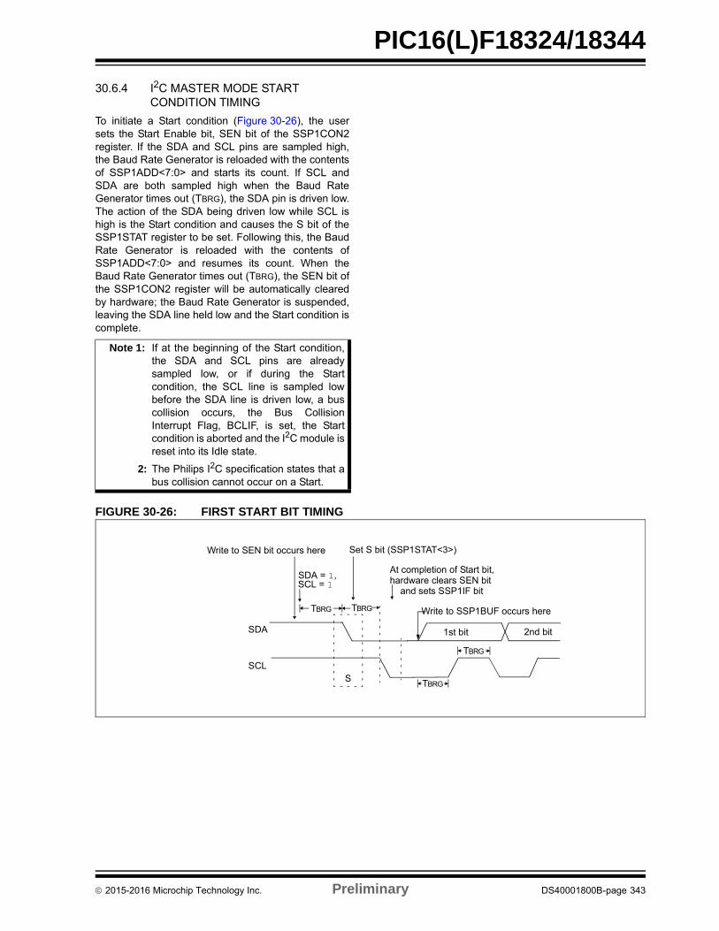
PIC16(L)F18324/18344
30.6.4 I2C MASTER MODE START CONDITION TIMING
To initiate a Start condition (Figure 30-26), the usersets the Start Enable bit, SEN bit of the SSP1CON2register. If the SDA and SCL pins are sampled high,the Baud Rate Generator is reloaded with the contentsof SSP1ADD<7:0> and starts its count. If SCL andSDA are both sampled high when the Baud RateGenerator times out (TBRG), the SDA pin is driven low.The action of the SDA being driven low while SCL ishigh is the Start condition and causes the S bit of theSSP1STAT register to be set. Following this, the BaudRate Generator is reloaded with the contents ofSSP1ADD<7:0> and resumes its count. When theBaud Rate Generator times out (TBRG), the SEN bit ofthe SSP1CON2 register will be automatically clearedby hardware; the Baud Rate Generator is suspended,leaving the SDA line held low and the Start condition iscomplete.
FIGURE 30-26: FIRST START BIT TIMING
Note 1: If at the beginning of the Start condition,the SDA and SCL pins are alreadysampled low, or if during the Startcondition, the SCL line is sampled lowbefore the SDA line is driven low, a buscollision occurs, the Bus CollisionInterrupt Flag, BCLIF, is set, the Startcondition is aborted and the I2C module isreset into its Idle state.
2: The Philips I2C specification states that abus collision cannot occur on a Start.
SDA
SCLS
TBRG
1st bit 2nd bit
TBRG
SDA = 1, At completion of Start bit,
SCL = 1
Write to SSP1BUF occurs hereTBRG
hardware clears SEN bit
TBRG
Write to SEN bit occurs here Set S bit (SSP1STAT<3>)
and sets SSP1IF bit
2015-2016 Microchip Technology Inc. Preliminary DS40001800B-page 343
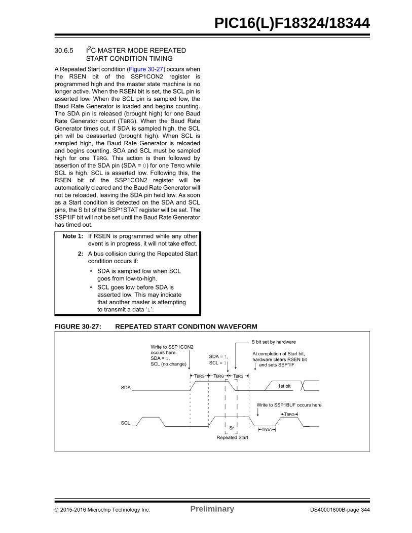
PIC16(L)F18324/18344
30.6.5 I2C MASTER MODE REPEATED START CONDITION TIMING
A Repeated Start condition (Figure 30-27) occurs whenthe RSEN bit of the SSP1CON2 register isprogrammed high and the master state machine is nolonger active. When the RSEN bit is set, the SCL pin isasserted low. When the SCL pin is sampled low, theBaud Rate Generator is loaded and begins counting.The SDA pin is released (brought high) for one BaudRate Generator count (TBRG). When the Baud RateGenerator times out, if SDA is sampled high, the SCLpin will be deasserted (brought high). When SCL issampled high, the Baud Rate Generator is reloadedand begins counting. SDA and SCL must be sampledhigh for one TBRG. This action is then followed byassertion of the SDA pin (SDA = 0) for one TBRG whileSCL is high. SCL is asserted low. Following this, theRSEN bit of the SSP1CON2 register will beautomatically cleared and the Baud Rate Generator willnot be reloaded, leaving the SDA pin held low. As soonas a Start condition is detected on the SDA and SCLpins, the S bit of the SSP1STAT register will be set. TheSSP1IF bit will not be set until the Baud Rate Generatorhas timed out.
FIGURE 30-27: REPEATED START CONDITION WAVEFORM
Note 1: If RSEN is programmed while any otherevent is in progress, it will not take effect.
2: A bus collision during the Repeated Startcondition occurs if:
• SDA is sampled low when SCL goes from low-to-high.
• SCL goes low before SDA is asserted low. This may indicate that another master is attempting to transmit a data ‘1’.
SDA
SCL
Repeated Start
Write to SSP1CON2
Write to SSP1BUF occurs here
At completion of Start bit, hardware clears RSEN bit
1st bit
S bit set by hardware
TBRG
TBRG
SDA = 1, SDA = 1,
SCL (no change) SCL = 1
occurs here
TBRG TBRG TBRG
and sets SSP1IF
Sr
2015-2016 Microchip Technology Inc. Preliminary DS40001800B-page 344
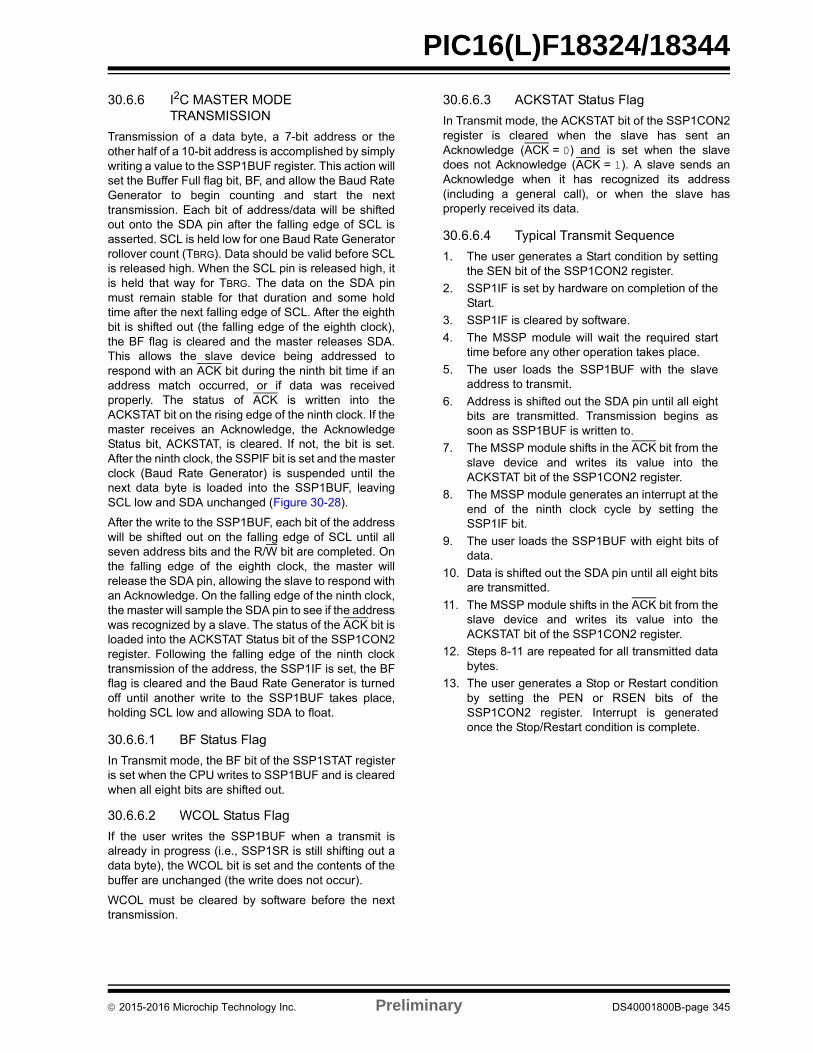
PIC16(L)F18324/18344
30.6.6 I2C MASTER MODE TRANSMISSION
Transmission of a data byte, a 7-bit address or theother half of a 10-bit address is accomplished by simplywriting a value to the SSP1BUF register. This action willset the Buffer Full flag bit, BF, and allow the Baud RateGenerator to begin counting and start the nexttransmission. Each bit of address/data will be shiftedout onto the SDA pin after the falling edge of SCL isasserted. SCL is held low for one Baud Rate Generatorrollover count (TBRG). Data should be valid before SCLis released high. When the SCL pin is released high, itis held that way for TBRG. The data on the SDA pinmust remain stable for that duration and some holdtime after the next falling edge of SCL. After the eighthbit is shifted out (the falling edge of the eighth clock),the BF flag is cleared and the master releases SDA.This allows the slave device being addressed torespond with an ACK bit during the ninth bit time if anaddress match occurred, or if data was receivedproperly. The status of ACK is written into theACKSTAT bit on the rising edge of the ninth clock. If themaster receives an Acknowledge, the AcknowledgeStatus bit, ACKSTAT, is cleared. If not, the bit is set.After the ninth clock, the SSPIF bit is set and the masterclock (Baud Rate Generator) is suspended until thenext data byte is loaded into the SSP1BUF, leavingSCL low and SDA unchanged (Figure 30-28).
After the write to the SSP1BUF, each bit of the addresswill be shifted out on the falling edge of SCL until allseven address bits and the R/W bit are completed. Onthe falling edge of the eighth clock, the master willrelease the SDA pin, allowing the slave to respond withan Acknowledge. On the falling edge of the ninth clock,the master will sample the SDA pin to see if the addresswas recognized by a slave. The status of the ACK bit isloaded into the ACKSTAT Status bit of the SSP1CON2register. Following the falling edge of the ninth clocktransmission of the address, the SSP1IF is set, the BFflag is cleared and the Baud Rate Generator is turnedoff until another write to the SSP1BUF takes place,holding SCL low and allowing SDA to float.
30.6.6.1 BF Status Flag
In Transmit mode, the BF bit of the SSP1STAT registeris set when the CPU writes to SSP1BUF and is clearedwhen all eight bits are shifted out.
30.6.6.2 WCOL Status Flag
If the user writes the SSP1BUF when a transmit isalready in progress (i.e., SSP1SR is still shifting out adata byte), the WCOL bit is set and the contents of thebuffer are unchanged (the write does not occur).
WCOL must be cleared by software before the nexttransmission.
30.6.6.3 ACKSTAT Status Flag
In Transmit mode, the ACKSTAT bit of the SSP1CON2register is cleared when the slave has sent anAcknowledge (ACK = 0) and is set when the slavedoes not Acknowledge (ACK = 1). A slave sends anAcknowledge when it has recognized its address(including a general call), or when the slave hasproperly received its data.
30.6.6.4 Typical Transmit Sequence
1. The user generates a Start condition by settingthe SEN bit of the SSP1CON2 register.
2. SSP1IF is set by hardware on completion of theStart.
3. SSP1IF is cleared by software.
4. The MSSP module will wait the required starttime before any other operation takes place.
5. The user loads the SSP1BUF with the slaveaddress to transmit.
6. Address is shifted out the SDA pin until all eightbits are transmitted. Transmission begins assoon as SSP1BUF is written to.
7. The MSSP module shifts in the ACK bit from theslave device and writes its value into theACKSTAT bit of the SSP1CON2 register.
8. The MSSP module generates an interrupt at theend of the ninth clock cycle by setting theSSP1IF bit.
9. The user loads the SSP1BUF with eight bits ofdata.
10. Data is shifted out the SDA pin until all eight bitsare transmitted.
11. The MSSP module shifts in the ACK bit from theslave device and writes its value into theACKSTAT bit of the SSP1CON2 register.
12. Steps 8-11 are repeated for all transmitted databytes.
13. The user generates a Stop or Restart conditionby setting the PEN or RSEN bits of theSSP1CON2 register. Interrupt is generatedonce the Stop/Restart condition is complete.
2015-2016 Microchip Technology Inc. Preliminary DS40001800B-page 345
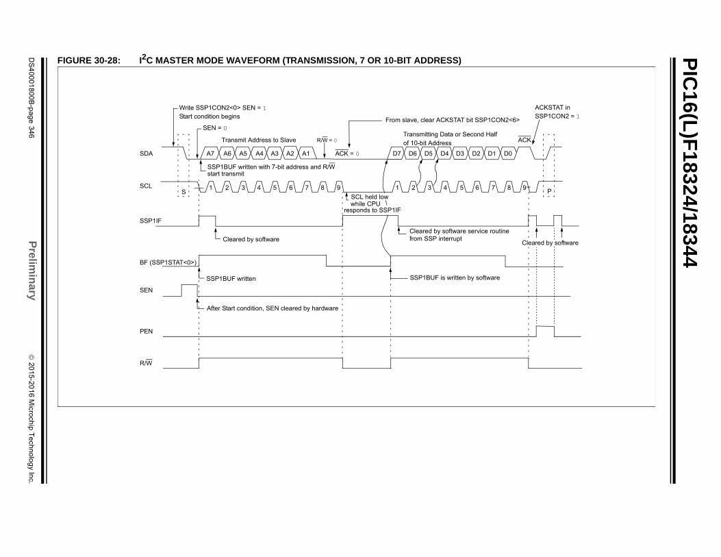
PIC
16(L)F
18324/18344
DS
40
00
18
00
B-p
ag
e 3
46
Prelim
inary
2
01
5-2
01
6 M
icroch
ip T
ech
no
log
y Inc.
1 D0
ACKlf
8 9P
outine
re
ON2<6>
ACKSTAT in SSP1CON2 = 1
Cleared by software
FIGURE 30-28: I2C MASTER MODE WAVEFORM (TRANSMISSION, 7 OR 10-BIT ADDRESS)
SDA
SCL
SSP1IF
BF (SSP1STAT<0>)
SEN
A7 A6 A5 A4 A3 A2 A1 ACK = 0 D7 D6 D5 D4 D3 D2 D
Transmitting Data or Second HaR/W = 0Transmit Address to Slave
1 2 3 4 5 6 7 8 9 1 2 3 4 5 6 7
Cleared by software service r
SSP1BUF is written by softwa
from SSP interrupt
After Start condition, SEN cleared by hardware
S
SSP1BUF written with 7-bit address and R/Wstart transmit
SCL held lowwhile CPU
responds to SSP1IF
SEN = 0
of 10-bit Address
Write SSP1CON2<0> SEN = 1Start condition begins
From slave, clear ACKSTAT bit SSP1C
Cleared by software
SSP1BUF written
PEN
R/W
PIC16(L)F18324/18344
30.6.7 I2C MASTER MODE RECEPTION
Master mode reception (Figure 30-29) is enabled byprogramming the Receive Enable bit, RCEN bit of theSSP1CON2 register.
The Baud Rate Generator begins counting and on eachrollover, the state of the SCL pin changes(high-to-low/low-to-high) and data is shifted into theSSP1SR. After the falling edge of the eighth clock, thereceive enable flag is automatically cleared, thecontents of the SSP1SR are loaded into the SSP1BUF,the BF flag bit is set, the SSP1IF flag bit is set and theBaud Rate Generator is suspended from counting,holding SCL low. The MSSP is now in Idle stateawaiting the next command. When the buffer is read bythe CPU, the BF flag bit is automatically cleared. Theuser can then send an Acknowledge bit at the end ofreception by setting the Acknowledge SequenceEnable, ACKEN bit of the SSP1CON2 register.
30.6.7.1 BF Status Flag
In receive operation, the BF bit is set when an addressor data byte is loaded into SSP1BUF from SSP1SR. Itis cleared when the SSP1BUF register is read.
30.6.7.2 SSPOV Status Flag
In receive operation, the SSPOV bit is set when eightbits are received into the SSP1SR and the BF flag bit isalready set from a previous reception.
30.6.7.3 WCOL Status Flag
If the user writes the SSP1BUF when a receive isalready in progress (i.e., SSP1SR is still shifting in adata byte), the WCOL bit is set and the contents of thebuffer are unchanged (the write does not occur).
30.6.7.4 Typical Receive Sequence:
1. The user generates a Start condition by settingthe SEN bit of the SSP1CON2 register.
2. SSP1IF is set by hardware on completion of theStart.
3. SSP1IF is cleared by software.
4. User writes SSP1BUF with the slave address totransmit and the R/W bit set.
5. Address is shifted out the SDA pin until all eightbits are transmitted. Transmission begins assoon as SSP1BUF is written to.
6. The MSSP module shifts in the ACK bit from theslave device and writes its value into theACKSTAT bit of the SSP1CON2 register.
7. The MSSP module generates an interrupt at theend of the ninth clock cycle by setting theSSP1IF bit.
8. User sets the RCEN bit of the SSP1CON2 regis-ter and the master clocks in a byte from the slave.
9. After the eighth falling edge of SCL, SSP1IF andBF are set.
10. Master clears SSP1IF and reads the receivedbyte from SSP1BUF, clears BF.
11. Master sets ACK value sent to slave in ACKDTbit of the SSP1CON2 register and initiates theACK by setting the ACKEN bit.
12. Master’s ACK is clocked out to the slave andSSP1IF is set.
13. User clears SSPIF.
14. Steps 8-13 are repeated for each received bytefrom the slave.
15. Master sends a not ACK or Stop to endcommunication.
Note: The MSSP module must be in an Idlestate before the RCEN bit is set or theRCEN bit will be disregarded.
2015-2016 Microchip Technology Inc. Preliminary DS40001800B-page 347
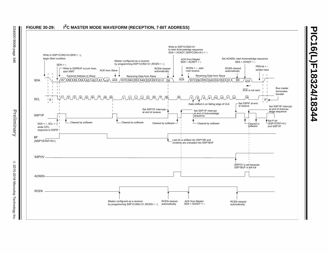
PIC
16(L)F
18324/18344
DS
40
00
18
00
B-p
ag
e 3
48
Prelim
inary
2
01
5-2
01
6 M
icroch
ip T
ech
no
log
y Inc.
P987
D0D1
Bus masterterminatestransfer
e
ACK is not sent
PEN bit = 1written here
CLK
ACK
Set P bit (SSP1STAT<4>)and SSP1IF
Cleared insoftware
Set SSPIF at endSet SSP1IF interruptat end of Acknow-ledge sequence
of receive
t ACKEN, start Acknowledge sequence
SSPOV is set becauseSSP1BUF is still full
SDA = ACKDT = 1
RCEN clearedautomatically
RCEN clearedautomatically
FIGURE 30-29: I2C MASTER MODE WAVEFORM (RECEPTION, 7-BIT ADDRESS)
65
D2D3D4D5D6D7
S
A7 A6 A5 A4 A3 A2 A1SDA
SCL 1 2 3 4 5 6 7 8 9 1 2 3 4 5 6 7 8 9 1 2 3 4
ACK
Receiving Data from SlavReceiving Data from Slave
D0D1D2D3D4D5D6D7ACKR/W
Transmit Address to Slave
SSP1IF
BF
Write to SSP1CON2<0>(SEN = 1),
Write to SSPBUF occurs here,ACK from Slave
Master configured as a receiverby programming SSP1CON2<3> (RCEN = 1)
Data shifted in on falling edge of
Cleared by software
start XMIT
SEN = 0
SSPOV
SDA = 0, SCL = 1while CPU
(SSP1STAT<0>)
Cleared by softwareCleared by software
Set SSP1IF interruptat end of receive
ACK from Master
Set SSP1IF interruptat end of Acknowledgesequence
Se
RCEN = 1, startnext receive
Write to SSP1CON2<4>to start Acknowledge sequenceSDA = ACKDT (SSPCON2<5>) = 0
RCEN clearedautomatically
responds to SSPIF
ACKEN
begin Start condition
Cleared by software
SDA = ACKDT = 0
Last bit is shifted into SSP1SR andcontents are unloaded into SSP1BUF
RCEN
Master configured as a receiverby programming SSP1CON2<3> (RCEN = 1)
RCEN clearedautomatically
ACK from MasterSDA = ACKDT = 0
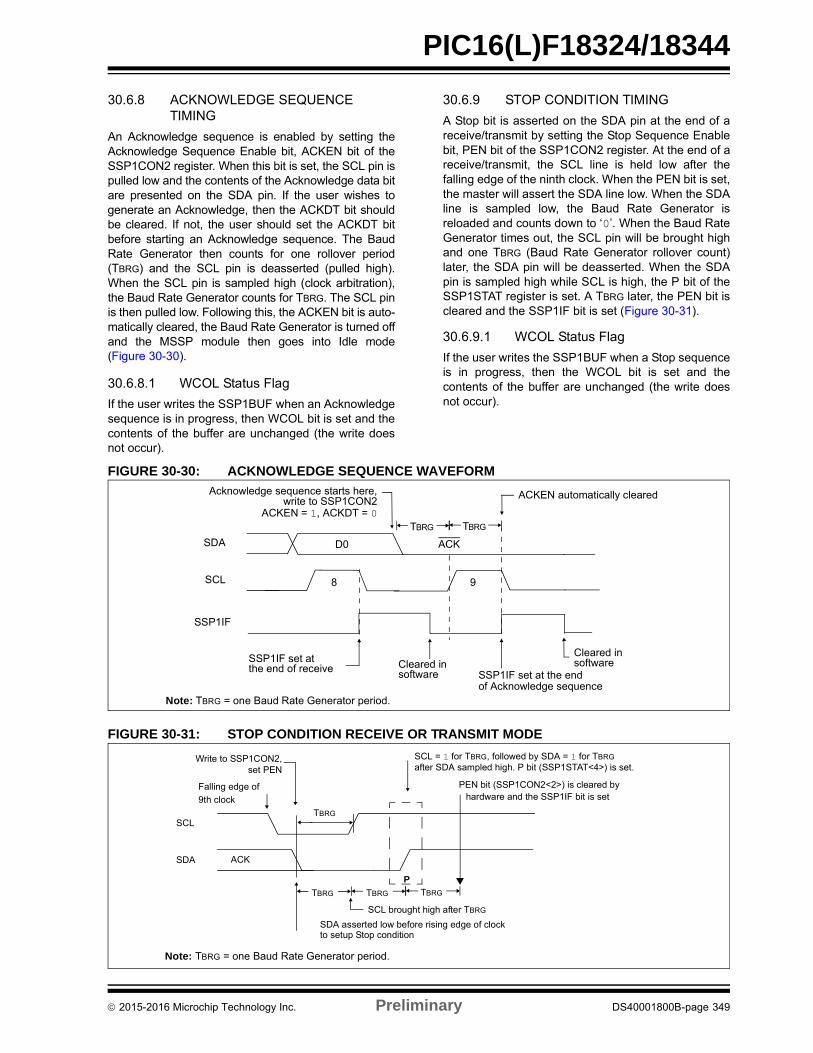
PIC16(L)F18324/18344
30.6.8 ACKNOWLEDGE SEQUENCE TIMING
An Acknowledge sequence is enabled by setting theAcknowledge Sequence Enable bit, ACKEN bit of theSSP1CON2 register. When this bit is set, the SCL pin ispulled low and the contents of the Acknowledge data bitare presented on the SDA pin. If the user wishes togenerate an Acknowledge, then the ACKDT bit shouldbe cleared. If not, the user should set the ACKDT bitbefore starting an Acknowledge sequence. The BaudRate Generator then counts for one rollover period(TBRG) and the SCL pin is deasserted (pulled high).When the SCL pin is sampled high (clock arbitration),the Baud Rate Generator counts for TBRG. The SCL pinis then pulled low. Following this, the ACKEN bit is auto-matically cleared, the Baud Rate Generator is turned offand the MSSP module then goes into Idle mode(Figure 30-30).
30.6.8.1 WCOL Status Flag
If the user writes the SSP1BUF when an Acknowledgesequence is in progress, then WCOL bit is set and thecontents of the buffer are unchanged (the write doesnot occur).
30.6.9 STOP CONDITION TIMING
A Stop bit is asserted on the SDA pin at the end of areceive/transmit by setting the Stop Sequence Enablebit, PEN bit of the SSP1CON2 register. At the end of areceive/transmit, the SCL line is held low after thefalling edge of the ninth clock. When the PEN bit is set,the master will assert the SDA line low. When the SDAline is sampled low, the Baud Rate Generator isreloaded and counts down to ‘0’. When the Baud RateGenerator times out, the SCL pin will be brought highand one TBRG (Baud Rate Generator rollover count)later, the SDA pin will be deasserted. When the SDApin is sampled high while SCL is high, the P bit of theSSP1STAT register is set. A TBRG later, the PEN bit iscleared and the SSP1IF bit is set (Figure 30-31).
30.6.9.1 WCOL Status Flag
If the user writes the SSP1BUF when a Stop sequenceis in progress, then the WCOL bit is set and thecontents of the buffer are unchanged (the write doesnot occur).
FIGURE 30-30: ACKNOWLEDGE SEQUENCE WAVEFORM
FIGURE 30-31: STOP CONDITION RECEIVE OR TRANSMIT MODE
Note: TBRG = one Baud Rate Generator period.
SDA
SCL
SSP1IF set at
Acknowledge sequence starts here,write to SSP1CON2
ACKEN automatically cleared
Cleared in
TBRG TBRG
the end of receive
8
ACKEN = 1, ACKDT = 0
D0
9
SSP1IF
software SSP1IF set at the endof Acknowledge sequence
Cleared insoftware
ACK
SCL
SDA
SDA asserted low before rising edge of clock
Write to SSP1CON2,set PEN
Falling edge of
SCL = 1 for TBRG, followed by SDA = 1 for TBRG
9th clock
SCL brought high after TBRG
Note: TBRG = one Baud Rate Generator period.
TBRG TBRG
after SDA sampled high. P bit (SSP1STAT<4>) is set.
TBRG
to setup Stop condition
ACK
P
TBRG
PEN bit (SSP1CON2<2>) is cleared by hardware and the SSP1IF bit is set
2015-2016 Microchip Technology Inc. Preliminary DS40001800B-page 349
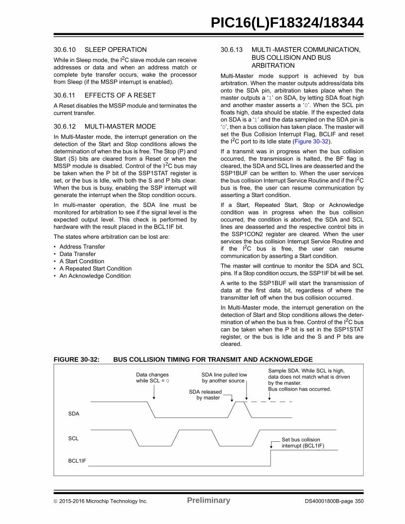
PIC16(L)F18324/18344
30.6.10 SLEEP OPERATION
While in Sleep mode, the I2C slave module can receiveaddresses or data and when an address match orcomplete byte transfer occurs, wake the processorfrom Sleep (if the MSSP interrupt is enabled).
30.6.11 EFFECTS OF A RESET
A Reset disables the MSSP module and terminates thecurrent transfer.
30.6.12 MULTI-MASTER MODE
In Multi-Master mode, the interrupt generation on thedetection of the Start and Stop conditions allows thedetermination of when the bus is free. The Stop (P) andStart (S) bits are cleared from a Reset or when theMSSP module is disabled. Control of the I2C bus maybe taken when the P bit of the SSP1STAT register isset, or the bus is Idle, with both the S and P bits clear.When the bus is busy, enabling the SSP interrupt willgenerate the interrupt when the Stop condition occurs.
In multi-master operation, the SDA line must bemonitored for arbitration to see if the signal level is theexpected output level. This check is performed byhardware with the result placed in the BCL1IF bit.
The states where arbitration can be lost are:
• Address Transfer • Data Transfer• A Start Condition • A Repeated Start Condition• An Acknowledge Condition
30.6.13 MULTI -MASTER COMMUNICATION, BUS COLLISION AND BUS ARBITRATION
Multi-Master mode support is achieved by busarbitration. When the master outputs address/data bitsonto the SDA pin, arbitration takes place when themaster outputs a ‘1’ on SDA, by letting SDA float highand another master asserts a ‘0’. When the SCL pinfloats high, data should be stable. If the expected dataon SDA is a ‘1’ and the data sampled on the SDA pin is‘0’, then a bus collision has taken place. The master willset the Bus Collision Interrupt Flag, BCLIF and resetthe I2C port to its Idle state (Figure 30-32).
If a transmit was in progress when the bus collisionoccurred, the transmission is halted, the BF flag iscleared, the SDA and SCL lines are deasserted and theSSP1BUF can be written to. When the user servicesthe bus collision Interrupt Service Routine and if the I2Cbus is free, the user can resume communication byasserting a Start condition.
If a Start, Repeated Start, Stop or Acknowledgecondition was in progress when the bus collisionoccurred, the condition is aborted, the SDA and SCLlines are deasserted and the respective control bits inthe SSP1CON2 register are cleared. When the userservices the bus collision Interrupt Service Routine andif the I2C bus is free, the user can resumecommunication by asserting a Start condition.
The master will continue to monitor the SDA and SCLpins. If a Stop condition occurs, the SSP1IF bit will be set.
A write to the SSP1BUF will start the transmission ofdata at the first data bit, regardless of where thetransmitter left off when the bus collision occurred.
In Multi-Master mode, the interrupt generation on thedetection of Start and Stop conditions allows the deter-mination of when the bus is free. Control of the I2C buscan be taken when the P bit is set in the SSP1STATregister, or the bus is Idle and the S and P bits arecleared.
FIGURE 30-32: BUS COLLISION TIMING FOR TRANSMIT AND ACKNOWLEDGE
SDA
SCL
BCL1IF
SDA released
SDA line pulled lowby another source
Sample SDA. While SCL is high,data does not match what is driven
Bus collision has occurred.
Set bus collisioninterrupt (BCL1IF)
by the master.
by master
Data changeswhile SCL = 0
2015-2016 Microchip Technology Inc. Preliminary DS40001800B-page 350
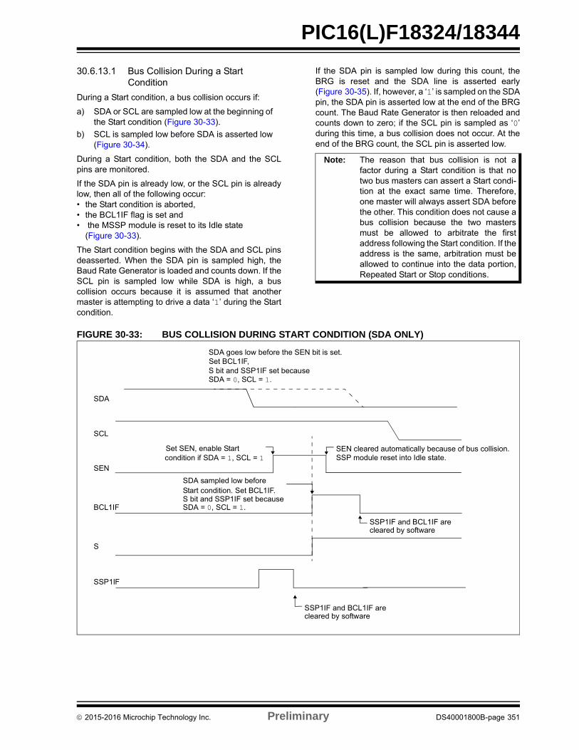
PIC16(L)F18324/18344
30.6.13.1 Bus Collision During a Start Condition
During a Start condition, a bus collision occurs if:
a) SDA or SCL are sampled low at the beginning ofthe Start condition (Figure 30-33).
b) SCL is sampled low before SDA is asserted low(Figure 30-34).
During a Start condition, both the SDA and the SCLpins are monitored.
If the SDA pin is already low, or the SCL pin is alreadylow, then all of the following occur:• the Start condition is aborted, • the BCL1IF flag is set and• the MSSP module is reset to its Idle state
(Figure 30-33).
The Start condition begins with the SDA and SCL pinsdeasserted. When the SDA pin is sampled high, theBaud Rate Generator is loaded and counts down. If theSCL pin is sampled low while SDA is high, a buscollision occurs because it is assumed that anothermaster is attempting to drive a data ‘1’ during the Startcondition.
If the SDA pin is sampled low during this count, theBRG is reset and the SDA line is asserted early(Figure 30-35). If, however, a ‘1’ is sampled on the SDApin, the SDA pin is asserted low at the end of the BRGcount. The Baud Rate Generator is then reloaded andcounts down to zero; if the SCL pin is sampled as ‘0’during this time, a bus collision does not occur. At theend of the BRG count, the SCL pin is asserted low.
FIGURE 30-33: BUS COLLISION DURING START CONDITION (SDA ONLY)
Note: The reason that bus collision is not afactor during a Start condition is that notwo bus masters can assert a Start condi-tion at the exact same time. Therefore,one master will always assert SDA beforethe other. This condition does not cause abus collision because the two mastersmust be allowed to arbitrate the firstaddress following the Start condition. If theaddress is the same, arbitration must beallowed to continue into the data portion,Repeated Start or Stop conditions.
SDA
SCL
SEN
SDA sampled low before
SDA goes low before the SEN bit is set.
S bit and SSP1IF set because
SSP module reset into Idle state.SEN cleared automatically because of bus collision.
S bit and SSP1IF set because
Set SEN, enable Startcondition if SDA = 1, SCL = 1
SDA = 0, SCL = 1.
BCL1IF
S
SSP1IF
SDA = 0, SCL = 1.
SSP1IF and BCL1IF arecleared by software
SSP1IF and BCL1IF arecleared by software
Set BCL1IF,
Start condition. Set BCL1IF.
2015-2016 Microchip Technology Inc. Preliminary DS40001800B-page 351
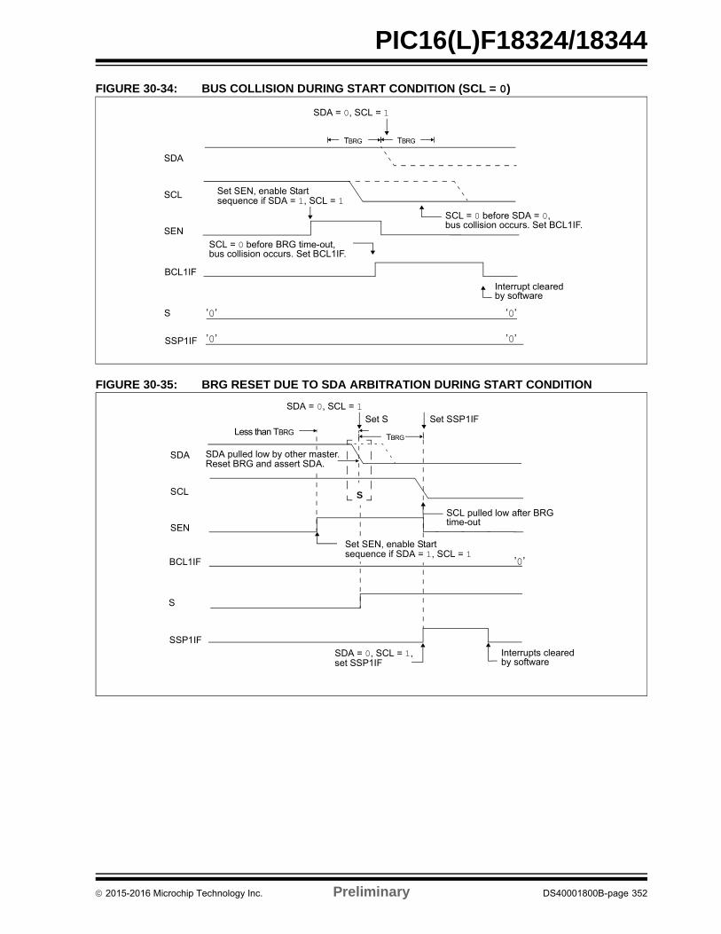
PIC16(L)F18324/18344
FIGURE 30-34: BUS COLLISION DURING START CONDITION (SCL = 0)
FIGURE 30-35: BRG RESET DUE TO SDA ARBITRATION DURING START CONDITION
SDA
SCL
SENbus collision occurs. Set BCL1IF.SCL = 0 before SDA = 0,
Set SEN, enable Startsequence if SDA = 1, SCL = 1
TBRG TBRG
SDA = 0, SCL = 1
BCL1IF
S
SSP1IF
Interrupt clearedby software
bus collision occurs. Set BCL1IF.SCL = 0 before BRG time-out,
’0’ ’0’
’0’’0’
SDA
SCL
SEN
Set SLess than TBRG
TBRG
SDA = 0, SCL = 1
BCL1IF
S
SSP1IF
S
Interrupts clearedby softwareset SSP1IF
SDA = 0, SCL = 1,
SCL pulled low after BRGtime-out
Set SSP1IF
’0’
SDA pulled low by other master.Reset BRG and assert SDA.
Set SEN, enable Startsequence if SDA = 1, SCL = 1
2015-2016 Microchip Technology Inc. Preliminary DS40001800B-page 352
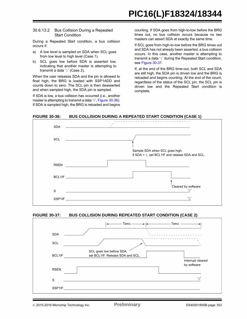
PIC16(L)F18324/18344
30.6.13.2 Bus Collision During a Repeated Start Condition
During a Repeated Start condition, a bus collisionoccurs if:
a) A low level is sampled on SDA when SCL goesfrom low level to high level (Case 1).
b) SCL goes low before SDA is asserted low,indicating that another master is attempting totransmit a data ‘1’ (Case 2).
When the user releases SDA and the pin is allowed tofloat high, the BRG is loaded with SSP1ADD andcounts down to zero. The SCL pin is then deassertedand when sampled high, the SDA pin is sampled.
If SDA is low, a bus collision has occurred (i.e., anothermaster is attempting to transmit a data ‘0’, Figure 30-36).If SDA is sampled high, the BRG is reloaded and begins
counting. If SDA goes from high-to-low before the BRGtimes out, no bus collision occurs because no twomasters can assert SDA at exactly the same time.
If SCL goes from high-to-low before the BRG times outand SDA has not already been asserted, a bus collisionoccurs. In this case, another master is attempting totransmit a data ‘1’ during the Repeated Start condition,see Figure 30-37.
If, at the end of the BRG time-out, both SCL and SDAare still high, the SDA pin is driven low and the BRG isreloaded and begins counting. At the end of the count,regardless of the status of the SCL pin, the SCL pin isdriven low and the Repeated Start condition iscomplete.
FIGURE 30-36: BUS COLLISION DURING A REPEATED START CONDITION (CASE 1)
FIGURE 30-37: BUS COLLISION DURING REPEATED START CONDITION (CASE 2)
SDA
SCL
RSEN
BCL1IF
S
SSP1IF
Sample SDA when SCL goes high.If SDA = 0, set BCL1IF and release SDA and SCL.
Cleared by software
’0’
’0’
SDA
SCL
BCL1IF
RSEN
S
SSP1IF
Interrupt clearedby software
SCL goes low before SDA,set BCL1IF. Release SDA and SCL.
TBRG TBRG
’0’
2015-2016 Microchip Technology Inc. Preliminary DS40001800B-page 353
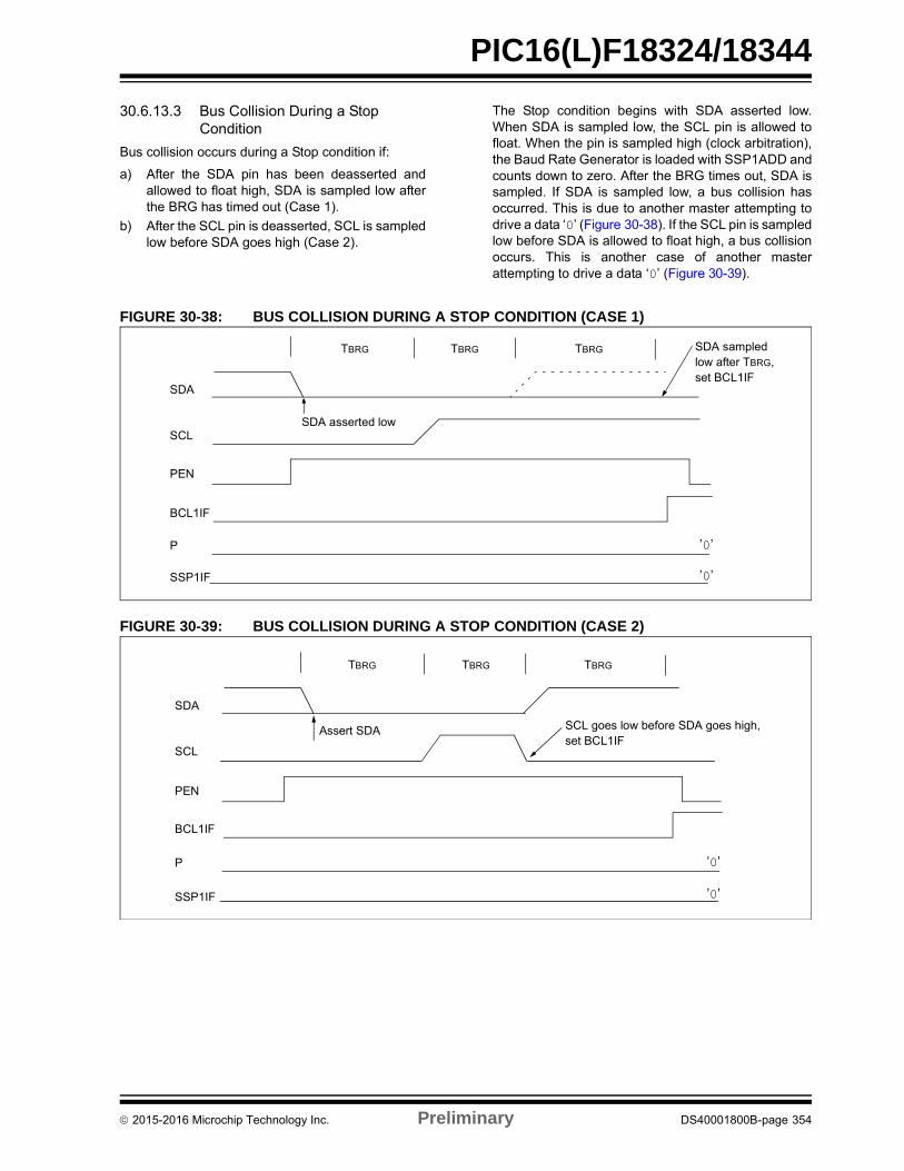
PIC16(L)F18324/18344
30.6.13.3 Bus Collision During a Stop Condition
Bus collision occurs during a Stop condition if:
a) After the SDA pin has been deasserted andallowed to float high, SDA is sampled low afterthe BRG has timed out (Case 1).
b) After the SCL pin is deasserted, SCL is sampledlow before SDA goes high (Case 2).
The Stop condition begins with SDA asserted low.When SDA is sampled low, the SCL pin is allowed tofloat. When the pin is sampled high (clock arbitration),the Baud Rate Generator is loaded with SSP1ADD andcounts down to zero. After the BRG times out, SDA issampled. If SDA is sampled low, a bus collision hasoccurred. This is due to another master attempting todrive a data ‘0’ (Figure 30-38). If the SCL pin is sampledlow before SDA is allowed to float high, a bus collisionoccurs. This is another case of another masterattempting to drive a data ‘0’ (Figure 30-39).
FIGURE 30-38: BUS COLLISION DURING A STOP CONDITION (CASE 1)
FIGURE 30-39: BUS COLLISION DURING A STOP CONDITION (CASE 2)
SDA
SCL
BCL1IF
PEN
P
SSP1IF
TBRG TBRG TBRG
SDA asserted low
SDA sampledlow after TBRG,set BCL1IF
’0’
’0’
SDA
SCL
BCL1IF
PEN
P
SSP1IF
TBRG TBRG TBRG
Assert SDA SCL goes low before SDA goes high,set BCL1IF
’0’
’0’
2015-2016 Microchip Technology Inc. Preliminary DS40001800B-page 354
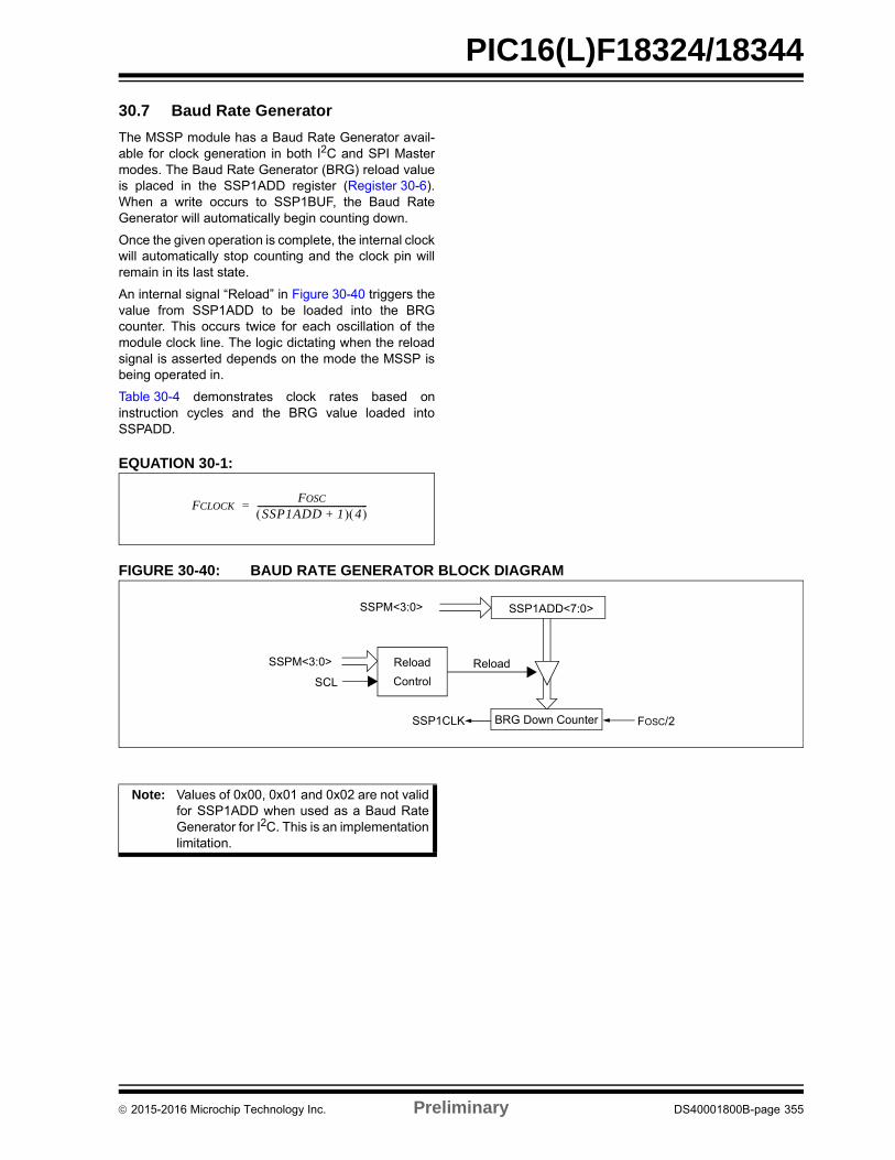
PIC16(L)F18324/18344
30.7 Baud Rate Generator
The MSSP module has a Baud Rate Generator avail-able for clock generation in both I2C and SPI Mastermodes. The Baud Rate Generator (BRG) reload valueis placed in the SSP1ADD register (Register 30-6).When a write occurs to SSP1BUF, the Baud RateGenerator will automatically begin counting down.
Once the given operation is complete, the internal clockwill automatically stop counting and the clock pin willremain in its last state.
An internal signal “Reload” in Figure 30-40 triggers thevalue from SSP1ADD to be loaded into the BRGcounter. This occurs twice for each oscillation of themodule clock line. The logic dictating when the reloadsignal is asserted depends on the mode the MSSP isbeing operated in.
Table 30-4 demonstrates clock rates based oninstruction cycles and the BRG value loaded intoSSPADD.
EQUATION 30-1:
FIGURE 30-40: BAUD RATE GENERATOR BLOCK DIAGRAM
FCLOCKFOSC
SSP1ADD 1+ 4 --------------------------------------------------=
Note: Values of 0x00, 0x01 and 0x02 are not validfor SSP1ADD when used as a Baud RateGenerator for I2C. This is an implementationlimitation.
SSPM<3:0>
BRG Down CounterSSP1CLK FOSC/2
SSP1ADD<7:0>
SSPM<3:0>
SCL
Reload
Control
Reload
2015-2016 Microchip Technology Inc. Preliminary DS40001800B-page 355
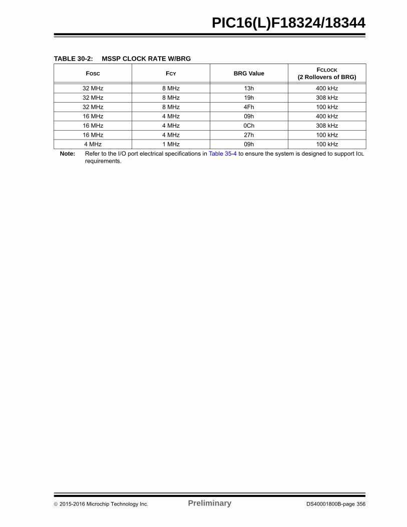
PIC16(L)F18324/18344
TABLE 30-2: MSSP CLOCK RATE W/BRG
FOSC FCY BRG ValueFCLOCK
(2 Rollovers of BRG)
32 MHz 8 MHz 13h 400 kHz
32 MHz 8 MHz 19h 308 kHz
32 MHz 8 MHz 4Fh 100 kHz
16 MHz 4 MHz 09h 400 kHz
16 MHz 4 MHz 0Ch 308 kHz
16 MHz 4 MHz 27h 100 kHz
4 MHz 1 MHz 09h 100 kHz
Note: Refer to the I/O port electrical specifications in Table 35-4 to ensure the system is designed to support IOL
requirements.
2015-2016 Microchip Technology Inc. Preliminary DS40001800B-page 356
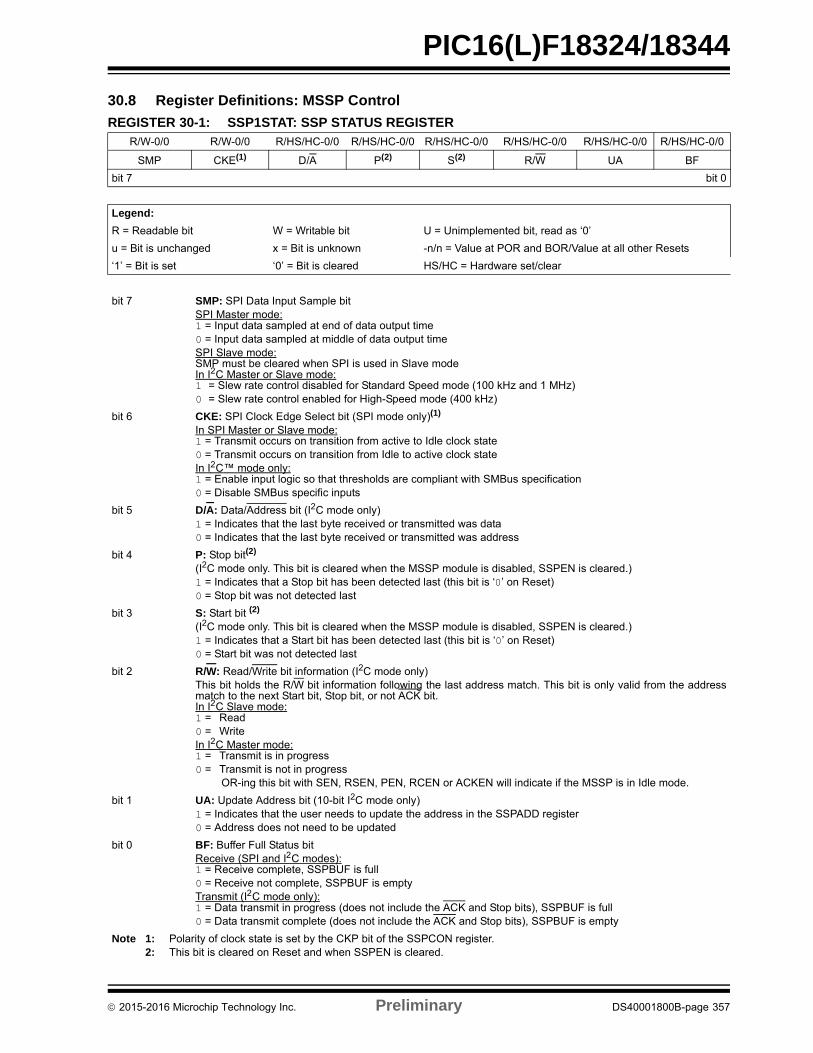
PIC16(L)F18324/18344
30.8 Register Definitions: MSSP Control
REGISTER 30-1: SSP1STAT: SSP STATUS REGISTERR/W-0/0 R/W-0/0 R/HS/HC-0/0 R/HS/HC-0/0 R/HS/HC-0/0 R/HS/HC-0/0 R/HS/HC-0/0 R/HS/HC-0/0
SMP CKE(1) D/A P(2) S(2) R/W UA BF
bit 7 bit 0
Legend:
R = Readable bit W = Writable bit U = Unimplemented bit, read as ‘0’
u = Bit is unchanged x = Bit is unknown -n/n = Value at POR and BOR/Value at all other Resets
‘1’ = Bit is set ‘0’ = Bit is cleared HS/HC = Hardware set/clear
bit 7 SMP: SPI Data Input Sample bitSPI Master mode:1 = Input data sampled at end of data output time0 = Input data sampled at middle of data output timeSPI Slave mode:SMP must be cleared when SPI is used in Slave modeIn I2 C Master or Slave mode: 1 = Slew rate control disabled for Standard Speed mode (100 kHz and 1 MHz)0 = Slew rate control enabled for High-Speed mode (400 kHz)
bit 6 CKE: SPI Clock Edge Select bit (SPI mode only)(1)
In SPI Master or Slave mode:1 = Transmit occurs on transition from active to Idle clock state0 = Transmit occurs on transition from Idle to active clock stateIn I2 C™ mode only: 1 = Enable input logic so that thresholds are compliant with SMBus specification0 = Disable SMBus specific inputs
bit 5 D/A: Data/Address bit (I2C mode only) 1 = Indicates that the last byte received or transmitted was data0 = Indicates that the last byte received or transmitted was address
bit 4 P: Stop bit(2)
(I2C mode only. This bit is cleared when the MSSP module is disabled, SSPEN is cleared.)1 = Indicates that a Stop bit has been detected last (this bit is ‘0’ on Reset)0 = Stop bit was not detected last
bit 3 S: Start bit (2)
(I2C mode only. This bit is cleared when the MSSP module is disabled, SSPEN is cleared.)1 = Indicates that a Start bit has been detected last (this bit is ‘0’ on Reset)0 = Start bit was not detected last
bit 2 R/W: Read/Write bit information (I2C mode only)This bit holds the R/W bit information following the last address match. This bit is only valid from the addressmatch to the next Start bit, Stop bit, or not ACK bit.In I2 C Slave mode:1 = Read0 = WriteIn I2 C Master mode:1 = Transmit is in progress0 = Transmit is not in progress
OR-ing this bit with SEN, RSEN, PEN, RCEN or ACKEN will indicate if the MSSP is in Idle mode.
bit 1 UA: Update Address bit (10-bit I2C mode only)1 = Indicates that the user needs to update the address in the SSPADD register0 = Address does not need to be updated
bit 0 BF: Buffer Full Status bitReceive (SPI and I2 C modes):1 = Receive complete, SSPBUF is full0 = Receive not complete, SSPBUF is emptyTransmit (I2 C mode only):1 = Data transmit in progress (does not include the ACK and Stop bits), SSPBUF is full0 = Data transmit complete (does not include the ACK and Stop bits), SSPBUF is empty
Note 1: Polarity of clock state is set by the CKP bit of the SSPCON register.2: This bit is cleared on Reset and when SSPEN is cleared.
2015-2016 Microchip Technology Inc. Preliminary DS40001800B-page 357
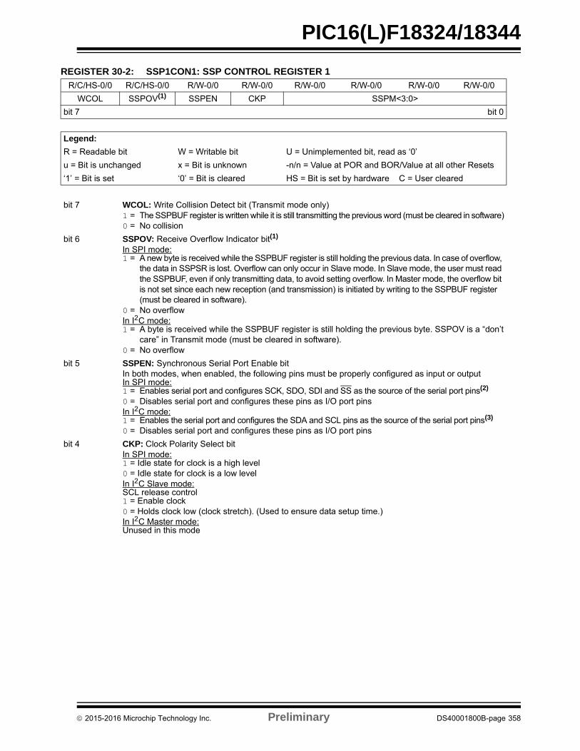
PIC16(L)F18324/18344
REGISTER 30-2: SSP1CON1: SSP CONTROL REGISTER 1R/C/HS-0/0 R/C/HS-0/0 R/W-0/0 R/W-0/0 R/W-0/0 R/W-0/0 R/W-0/0 R/W-0/0
WCOL SSPOV(1) SSPEN CKP SSPM<3:0>
bit 7 bit 0
Legend:
R = Readable bit W = Writable bit U = Unimplemented bit, read as ‘0’
u = Bit is unchanged x = Bit is unknown -n/n = Value at POR and BOR/Value at all other Resets
‘1’ = Bit is set ‘0’ = Bit is cleared HS = Bit is set by hardware C = User cleared
bit 7 WCOL: Write Collision Detect bit (Transmit mode only)1 = The SSPBUF register is written while it is still transmitting the previous word (must be cleared in software)0 = No collision
bit 6 SSPOV: Receive Overflow Indicator bit(1)
In SPI mode:1 = A new byte is received while the SSPBUF register is still holding the previous data. In case of overflow,
the data in SSPSR is lost. Overflow can only occur in Slave mode. In Slave mode, the user must read the SSPBUF, even if only transmitting data, to avoid setting overflow. In Master mode, the overflow bit is not set since each new reception (and transmission) is initiated by writing to the SSPBUF register (must be cleared in software).
0 = No overflowIn I2 C mode:1 = A byte is received while the SSPBUF register is still holding the previous byte. SSPOV is a “don’t
care” in Transmit mode (must be cleared in software). 0 = No overflow
bit 5 SSPEN: Synchronous Serial Port Enable bitIn both modes, when enabled, the following pins must be properly configured as input or outputIn SPI mode:1 = Enables serial port and configures SCK, SDO, SDI and SS as the source of the serial port pins(2)
0 = Disables serial port and configures these pins as I/O port pinsIn I2 C mode:1 = Enables the serial port and configures the SDA and SCL pins as the source of the serial port pins(3)
0 = Disables serial port and configures these pins as I/O port pins
bit 4 CKP: Clock Polarity Select bit In SPI mode:1 = Idle state for clock is a high level 0 = Idle state for clock is a low levelIn I2 C Slave mode:SCL release control1 = Enable clock 0 = Holds clock low (clock stretch). (Used to ensure data setup time.)In I2 C Master mode:Unused in this mode
2015-2016 Microchip Technology Inc. Preliminary DS40001800B-page 358
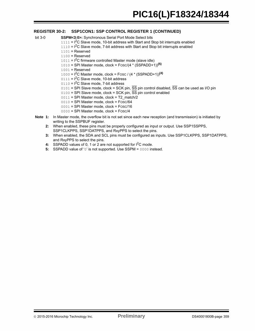
PIC16(L)F18324/18344
bit 3-0 SSPM<3:0>: Synchronous Serial Port Mode Select bits1111 = I2C Slave mode, 10-bit address with Start and Stop bit interrupts enabled 1110 = I2C Slave mode, 7-bit address with Start and Stop bit interrupts enabled 1101 = Reserved 1100 = Reserved 1011 = I2C firmware controlled Master mode (slave idle) 1010 = SPI Master mode, clock = FOSC/(4 * (SSPADD+1))(5)
1001 = Reserved1000 = I2C Master mode, clock = FOSC / (4 * (SSPADD+1))(4)
0111 = I2C Slave mode, 10-bit address 0110 = I2C Slave mode, 7-bit address 0101 = SPI Slave mode, clock = SCK pin, SS pin control disabled, SS can be used as I/O pin0100 = SPI Slave mode, clock = SCK pin, SS pin control enabled 0011 = SPI Master mode, clock = T2_match/2 0010 = SPI Master mode, clock = FOSC/64 0001 = SPI Master mode, clock = FOSC/16 0000 = SPI Master mode, clock = FOSC/4
Note 1: In Master mode, the overflow bit is not set since each new reception (and transmission) is initiated by writing to the SSPBUF register.
2: When enabled, these pins must be properly configured as input or output. Use SSP1SSPPS, SSP1CLKPPS, SSP1DATPPS, and RxyPPS to select the pins.
3: When enabled, the SDA and SCL pins must be configured as inputs. Use SSP1CLKPPS, SSP1DATPPS, and RxyPPS to select the pins.
4: SSPADD values of 0, 1 or 2 are not supported for I2C mode.5: SSPADD value of ‘0’ is not supported. Use SSPM = 0000 instead.
REGISTER 30-2: SSP1CON1: SSP CONTROL REGISTER 1 (CONTINUED)
2015-2016 Microchip Technology Inc. Preliminary DS40001800B-page 359
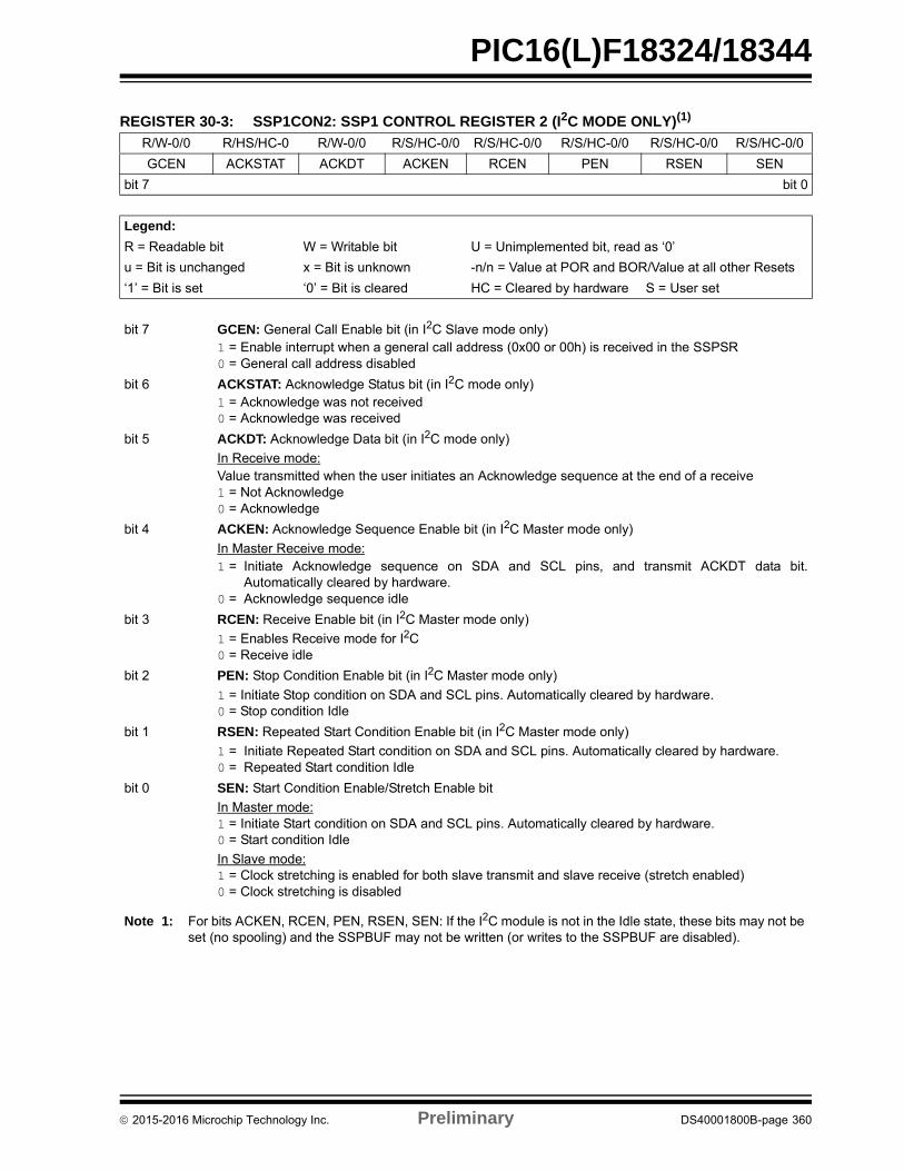
PIC16(L)F18324/18344
REGISTER 30-3: SSP1CON2: SSP1 CONTROL REGISTER 2 (I2C MODE ONLY)(1)
R/W-0/0 R/HS/HC-0 R/W-0/0 R/S/HC-0/0 R/S/HC-0/0 R/S/HC-0/0 R/S/HC-0/0 R/S/HC-0/0
GCEN ACKSTAT ACKDT ACKEN RCEN PEN RSEN SEN
bit 7 bit 0
Legend:
R = Readable bit W = Writable bit U = Unimplemented bit, read as ‘0’
u = Bit is unchanged x = Bit is unknown -n/n = Value at POR and BOR/Value at all other Resets
‘1’ = Bit is set ‘0’ = Bit is cleared HC = Cleared by hardware S = User set
bit 7 GCEN: General Call Enable bit (in I2C Slave mode only)1 = Enable interrupt when a general call address (0x00 or 00h) is received in the SSPSR0 = General call address disabled
bit 6 ACKSTAT: Acknowledge Status bit (in I2C mode only)1 = Acknowledge was not received0 = Acknowledge was received
bit 5 ACKDT: Acknowledge Data bit (in I2C mode only)
In Receive mode:Value transmitted when the user initiates an Acknowledge sequence at the end of a receive1 = Not Acknowledge0 = Acknowledge
bit 4 ACKEN: Acknowledge Sequence Enable bit (in I2C Master mode only)
In Master Receive mode:1 = Initiate Acknowledge sequence on SDA and SCL pins, and transmit ACKDT data bit.
Automatically cleared by hardware.0 = Acknowledge sequence idle
bit 3 RCEN: Receive Enable bit (in I2C Master mode only)
1 = Enables Receive mode for I2C0 = Receive idle
bit 2 PEN: Stop Condition Enable bit (in I2C Master mode only)
1 = Initiate Stop condition on SDA and SCL pins. Automatically cleared by hardware.0 = Stop condition Idle
bit 1 RSEN: Repeated Start Condition Enable bit (in I2C Master mode only)
1 = Initiate Repeated Start condition on SDA and SCL pins. Automatically cleared by hardware.0 = Repeated Start condition Idle
bit 0 SEN: Start Condition Enable/Stretch Enable bit
In Master mode:1 = Initiate Start condition on SDA and SCL pins. Automatically cleared by hardware.0 = Start condition Idle
In Slave mode:1 = Clock stretching is enabled for both slave transmit and slave receive (stretch enabled)0 = Clock stretching is disabled
Note 1: For bits ACKEN, RCEN, PEN, RSEN, SEN: If the I2C module is not in the Idle state, these bits may not be set (no spooling) and the SSPBUF may not be written (or writes to the SSPBUF are disabled).
2015-2016 Microchip Technology Inc. Preliminary DS40001800B-page 360
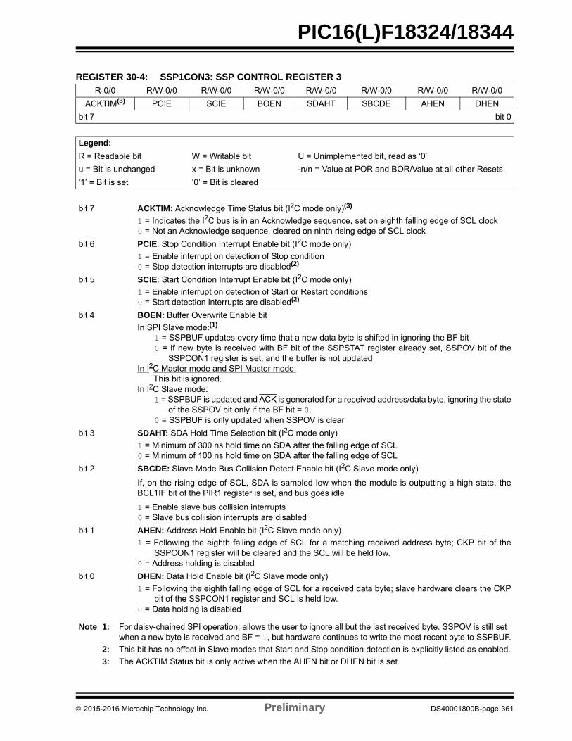
PIC16(L)F18324/18344
REGISTER 30-4: SSP1CON3: SSP CONTROL REGISTER 3
R-0/0 R/W-0/0 R/W-0/0 R/W-0/0 R/W-0/0 R/W-0/0 R/W-0/0 R/W-0/0
ACKTIM(3) PCIE SCIE BOEN SDAHT SBCDE AHEN DHEN
bit 7 bit 0
Legend:
R = Readable bit W = Writable bit U = Unimplemented bit, read as ‘0’
u = Bit is unchanged x = Bit is unknown -n/n = Value at POR and BOR/Value at all other Resets
‘1’ = Bit is set ‘0’ = Bit is cleared
bit 7 ACKTIM: Acknowledge Time Status bit (I2C mode only)(3)
1 = Indicates the I2C bus is in an Acknowledge sequence, set on eighth falling edge of SCL clock0 = Not an Acknowledge sequence, cleared on ninth rising edge of SCL clock
bit 6 PCIE: Stop Condition Interrupt Enable bit (I2C mode only)
1 = Enable interrupt on detection of Stop condition0 = Stop detection interrupts are disabled(2)
bit 5 SCIE: Start Condition Interrupt Enable bit (I2C mode only)
1 = Enable interrupt on detection of Start or Restart conditions0 = Start detection interrupts are disabled(2)
bit 4 BOEN: Buffer Overwrite Enable bit
In SPI Slave mode:(1)
1 = SSPBUF updates every time that a new data byte is shifted in ignoring the BF bit0 = If new byte is received with BF bit of the SSPSTAT register already set, SSPOV bit of the
SSPCON1 register is set, and the buffer is not updatedIn I2C Master mode and SPI Master mode:
This bit is ignored.In I2C Slave mode:
1 = SSPBUF is updated and ACK is generated for a received address/data byte, ignoring the stateof the SSPOV bit only if the BF bit = 0.
0 = SSPBUF is only updated when SSPOV is clear
bit 3 SDAHT: SDA Hold Time Selection bit (I2C mode only)
1 = Minimum of 300 ns hold time on SDA after the falling edge of SCL0 = Minimum of 100 ns hold time on SDA after the falling edge of SCL
bit 2 SBCDE: Slave Mode Bus Collision Detect Enable bit (I2C Slave mode only)
If, on the rising edge of SCL, SDA is sampled low when the module is outputting a high state, theBCL1IF bit of the PIR1 register is set, and bus goes idle
1 = Enable slave bus collision interrupts0 = Slave bus collision interrupts are disabled
bit 1 AHEN: Address Hold Enable bit (I2C Slave mode only)
1 = Following the eighth falling edge of SCL for a matching received address byte; CKP bit of theSSPCON1 register will be cleared and the SCL will be held low.
0 = Address holding is disabled
bit 0 DHEN: Data Hold Enable bit (I2C Slave mode only)
1 = Following the eighth falling edge of SCL for a received data byte; slave hardware clears the CKPbit of the SSPCON1 register and SCL is held low.
0 = Data holding is disabled
Note 1: For daisy-chained SPI operation; allows the user to ignore all but the last received byte. SSPOV is still set when a new byte is received and BF = 1, but hardware continues to write the most recent byte to SSPBUF.
2: This bit has no effect in Slave modes that Start and Stop condition detection is explicitly listed as enabled.
3: The ACKTIM Status bit is only active when the AHEN bit or DHEN bit is set.
2015-2016 Microchip Technology Inc. Preliminary DS40001800B-page 361
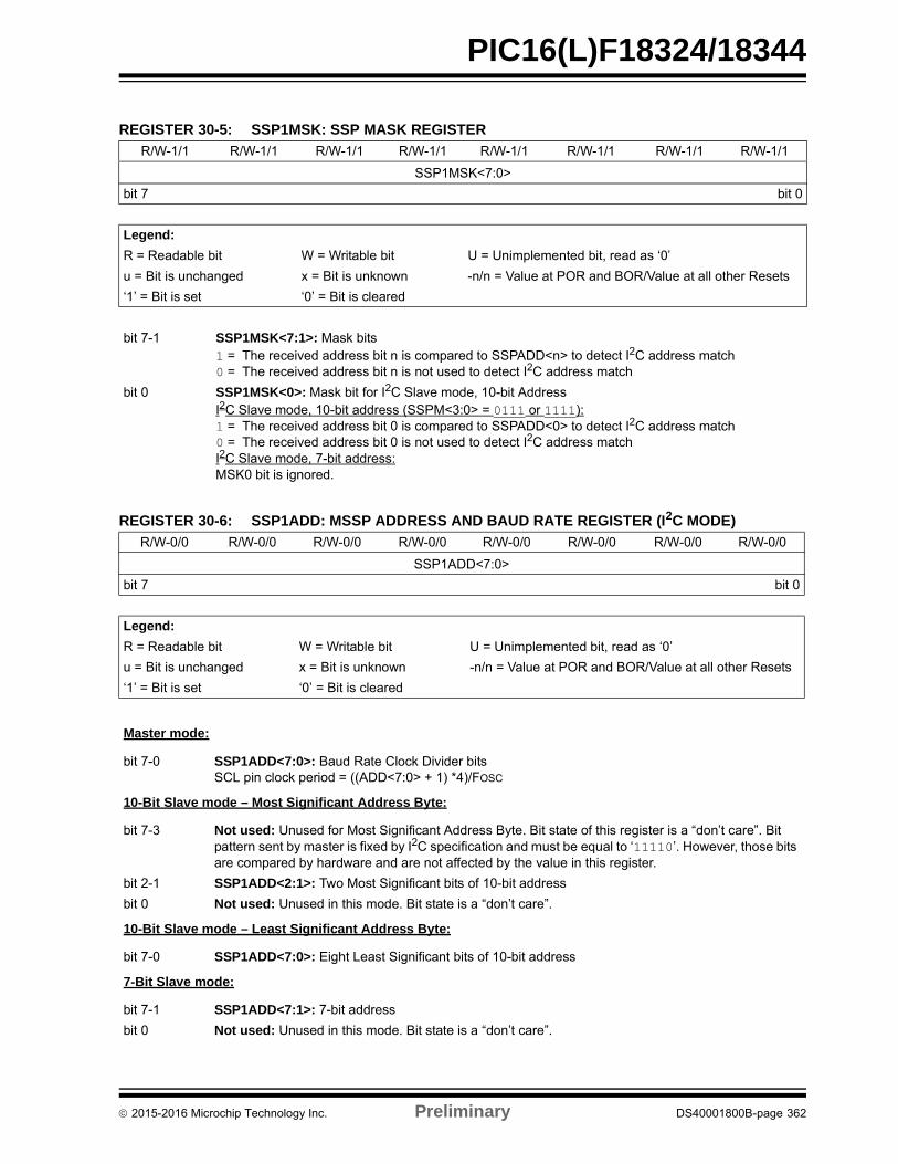
PIC16(L)F18324/18344
REGISTER 30-5: SSP1MSK: SSP MASK REGISTER
R/W-1/1 R/W-1/1 R/W-1/1 R/W-1/1 R/W-1/1 R/W-1/1 R/W-1/1 R/W-1/1
SSP1MSK<7:0>
bit 7 bit 0
Legend:
R = Readable bit W = Writable bit U = Unimplemented bit, read as ‘0’
u = Bit is unchanged x = Bit is unknown -n/n = Value at POR and BOR/Value at all other Resets
‘1’ = Bit is set ‘0’ = Bit is cleared
bit 7-1 SSP1MSK<7:1>: Mask bits1 = The received address bit n is compared to SSPADD<n> to detect I2C address match0 = The received address bit n is not used to detect I2C address match
bit 0 SSP1MSK<0>: Mask bit for I2C Slave mode, 10-bit AddressI2C Slave mode, 10-bit address (SSPM<3:0> = 0111 or 1111):1 = The received address bit 0 is compared to SSPADD<0> to detect I2C address match0 = The received address bit 0 is not used to detect I2C address matchI2C Slave mode, 7-bit address:MSK0 bit is ignored.
REGISTER 30-6: SSP1ADD: MSSP ADDRESS AND BAUD RATE REGISTER (I2C MODE)
R/W-0/0 R/W-0/0 R/W-0/0 R/W-0/0 R/W-0/0 R/W-0/0 R/W-0/0 R/W-0/0
SSP1ADD<7:0>
bit 7 bit 0
Legend:
R = Readable bit W = Writable bit U = Unimplemented bit, read as ‘0’
u = Bit is unchanged x = Bit is unknown -n/n = Value at POR and BOR/Value at all other Resets
‘1’ = Bit is set ‘0’ = Bit is cleared
Master mode:
bit 7-0 SSP1ADD<7:0>: Baud Rate Clock Divider bitsSCL pin clock period = ((ADD<7:0> + 1) *4)/FOSC
10-Bit Slave mode – Most Significant Address Byte:
bit 7-3 Not used: Unused for Most Significant Address Byte. Bit state of this register is a “don’t care”. Bit pattern sent by master is fixed by I2C specification and must be equal to ‘11110’. However, those bits are compared by hardware and are not affected by the value in this register.
bit 2-1 SSP1ADD<2:1>: Two Most Significant bits of 10-bit address
bit 0 Not used: Unused in this mode. Bit state is a “don’t care”.
10-Bit Slave mode – Least Significant Address Byte:
bit 7-0 SSP1ADD<7:0>: Eight Least Significant bits of 10-bit address
7-Bit Slave mode:
bit 7-1 SSP1ADD<7:1>: 7-bit address
bit 0 Not used: Unused in this mode. Bit state is a “don’t care”.
2015-2016 Microchip Technology Inc. Preliminary DS40001800B-page 362
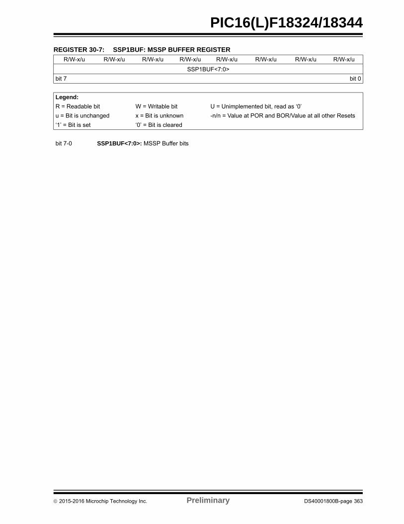
PIC16(L)F18324/18344
REGISTER 30-7: SSP1BUF: MSSP BUFFER REGISTER
R/W-x/u R/W-x/u R/W-x/u R/W-x/u R/W-x/u R/W-x/u R/W-x/u R/W-x/u
SSP1BUF<7:0>
bit 7 bit 0
Legend:
R = Readable bit W = Writable bit U = Unimplemented bit, read as ‘0’
u = Bit is unchanged x = Bit is unknown -n/n = Value at POR and BOR/Value at all other Resets
‘1’ = Bit is set ‘0’ = Bit is cleared
bit 7-0 SSP1BUF<7:0>: MSSP Buffer bits
2015-2016 Microchip Technology Inc. Preliminary DS40001800B-page 363
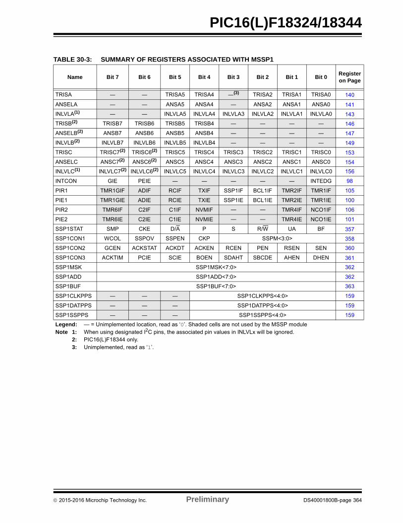
PIC16(L)F18324/18344
TABLE 30-3: SUMMARY OF REGISTERS ASSOCIATED WITH MSSP1
Name Bit 7 Bit 6 Bit 5 Bit 4 Bit 3 Bit 2 Bit 1 Bit 0Register on Page
TRISA ― ― TRISA5 TRISA4 ―(3) TRISA2 TRISA1 TRISA0 140
ANSELA ― ― ANSA5 ANSA4 ― ANSA2 ANSA1 ANSA0 141
INLVLA(1) ― ― INLVLA5 INLVLA4 INLVLA3 INLVLA2 INLVLA1 INLVLA0 143
TRISB(2) TRISB7 TRISB6 TRISB5 TRISB4 ― ― ― ― 146
ANSELB(2) ANSB7 ANSB6 ANSB5 ANSB4 ― ― ― ― 147
INLVLB(2) INLVLB7 INLVLB6 INLVLB5 INLVLB4 ― ― ― ― 149
TRISC TRISC7(2) TRISC6(2) TRISC5 TRISC4 TRISC3 TRISC2 TRISC1 TRISC0 153
ANSELC ANSC7(2) ANSC6(2) ANSC5 ANSC4 ANSC3 ANSC2 ANSC1 ANSC0 154
INLVLC(1) INLVLC7(2) INLVLC6(2) INLVLC5 INLVLC4 INLVLC3 INLVLC2 INLVLC1 INLVLC0 156
INTCON GIE PEIE ― ― ― ― ― INTEDG 98
PIR1 TMR1GIF ADIF RCIF TXIF SSP1IF BCL1IF TMR2IF TMR1IF 105
PIE1 TMR1GIE ADIE RCIE TXIE SSP1IE BCL1IE TMR2IE TMR1IE 100
PIR2 TMR6IF C2IF C1IF NVMIF ― ― TMR4IF NCO1IF 106
PIE2 TMR6IE C2IE C1IE NVMIE ― ― TMR4IE NCO1IE 101
SSP1STAT SMP CKE D/A P S R/W UA BF 357
SSP1CON1 WCOL SSPOV SSPEN CKP SSPM<3:0> 358
SSP1CON2 GCEN ACKSTAT ACKDT ACKEN RCEN PEN RSEN SEN 360
SSP1CON3 ACKTIM PCIE SCIE BOEN SDAHT SBCDE AHEN DHEN 361
SSP1MSK SSP1MSK<7:0> 362
SSP1ADD SSP1ADD<7:0> 362
SSP1BUF SSP1BUF<7:0> 363
SSP1CLKPPS ― ― ― SSP1CLKPPS<4:0> 159
SSP1DATPPS ― ― ― SSP1DATPPS<4:0> 159
SSP1SSPPS ― ― ― SSP1SSPPS<4:0> 159
Legend: — = Unimplemented location, read as ‘0’. Shaded cells are not used by the MSSP moduleNote 1: When using designated I2C pins, the associated pin values in INLVLx will be ignored.
2: PIC16(L)F18344 only.3: Unimplemented, read as ‘1’.
2015-2016 Microchip Technology Inc. Preliminary DS40001800B-page 364
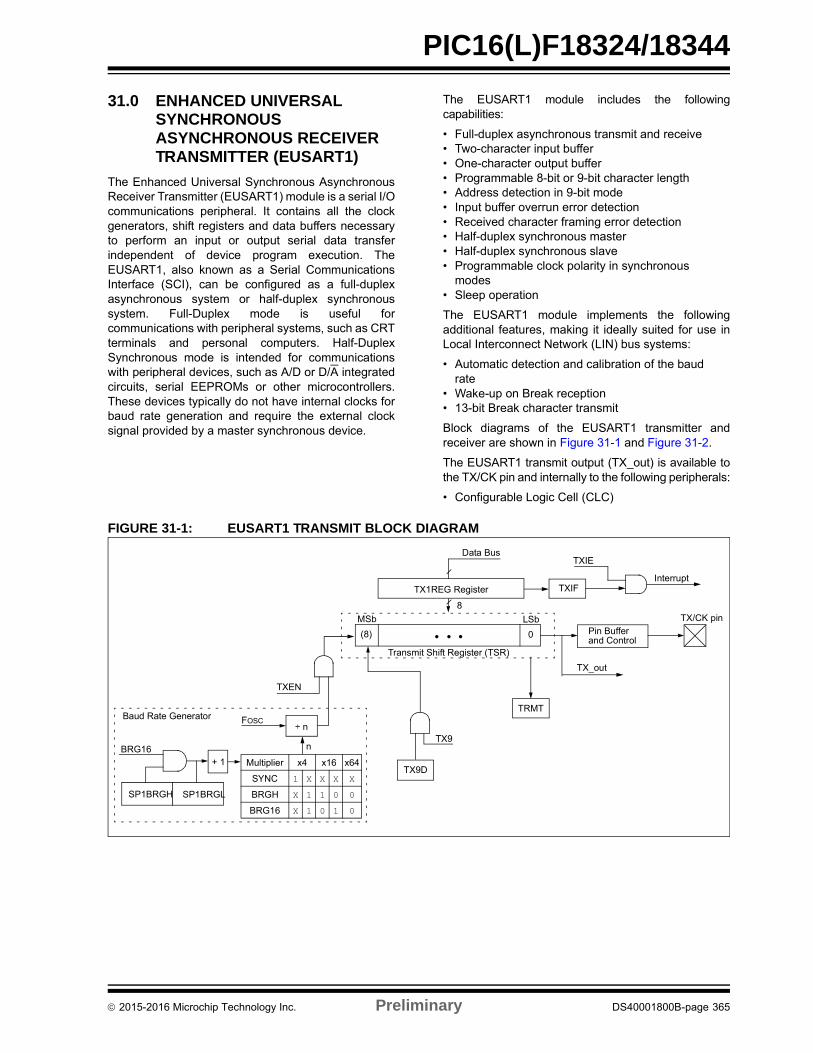
PIC16(L)F18324/18344
31.0 ENHANCED UNIVERSAL SYNCHRONOUS ASYNCHRONOUS RECEIVER TRANSMITTER (EUSART1)
The Enhanced Universal Synchronous AsynchronousReceiver Transmitter (EUSART1) module is a serial I/Ocommunications peripheral. It contains all the clockgenerators, shift registers and data buffers necessaryto perform an input or output serial data transferindependent of device program execution. TheEUSART1, also known as a Serial CommunicationsInterface (SCI), can be configured as a full-duplexasynchronous system or half-duplex synchronoussystem. Full-Duplex mode is useful forcommunications with peripheral systems, such as CRTterminals and personal computers. Half-DuplexSynchronous mode is intended for communicationswith peripheral devices, such as A/D or D/A integratedcircuits, serial EEPROMs or other microcontrollers.These devices typically do not have internal clocks forbaud rate generation and require the external clocksignal provided by a master synchronous device.
The EUSART1 module includes the followingcapabilities:
• Full-duplex asynchronous transmit and receive• Two-character input buffer• One-character output buffer• Programmable 8-bit or 9-bit character length• Address detection in 9-bit mode• Input buffer overrun error detection• Received character framing error detection• Half-duplex synchronous master• Half-duplex synchronous slave• Programmable clock polarity in synchronous
modes• Sleep operation
The EUSART1 module implements the followingadditional features, making it ideally suited for use inLocal Interconnect Network (LIN) bus systems:
• Automatic detection and calibration of the baud rate
• Wake-up on Break reception• 13-bit Break character transmit
Block diagrams of the EUSART1 transmitter andreceiver are shown in Figure 31-1 and Figure 31-2.
The EUSART1 transmit output (TX_out) is available tothe TX/CK pin and internally to the following peripherals:
• Configurable Logic Cell (CLC)
FIGURE 31-1: EUSART1 TRANSMIT BLOCK DIAGRAM
TXIF
TXIE
Interrupt
TXEN
TX9D
MSb LSb
Data Bus
TX1REG Register
Transmit Shift Register (TSR)
(8) 0
TX9
TRMT
TX/CK pin
Pin Bufferand Control
8
SP1BRGLSP1BRGH
BRG16
FOSC÷ n
n
+ 1 Multiplier x4 x16 x64
SYNC 1 X X X X
BRGH X 1 1 0 0
BRG16 X 1 0 1 0
Baud Rate Generator
• • •
TX_out
2015-2016 Microchip Technology Inc. Preliminary DS40001800B-page 365
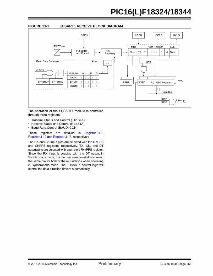
PIC16(L)F18324/18344
FIGURE 31-2: EUSART1 RECEIVE BLOCK DIAGRAM
The operation of the EUSART1 module is controlledthrough three registers:
• Transmit Status and Control (TX1STA)• Receive Status and Control (RC1STA)• Baud Rate Control (BAUD1CON)
These registers are detailed in Register 31-1,Register 31-2 and Register 31-3, respectively.
The RX and CK input pins are selected with the RXPPSand CKPPS registers, respectively. TX, CK, and DToutput pins are selected with each pin’s RxyPPS register.Since the RX input is coupled with the DT output inSynchronous mode, it is the user’s responsibility to selectthe same pin for both of these functions when operatingin Synchronous mode. The EUSART1 control logic willcontrol the data direction drivers automatically.
RX/DT pin
Pin Bufferand Control
SPEN
DataRecovery
CREN OERR
FERR
RSR RegisterMSb LSb
RX9D RC1REG RegisterFIFO
InterruptRCIFRCIE
Data Bus8
Stop Start(8) 7 1 0
RX9
• • •
SP1BRGLSP1BRGH
BRG16
RCIDL
FOSC÷ n
n+ 1 Multiplier x4 x16 x64
SYNC 1 X 0 0 0
BRGH X 1 1 0 0
BRG16 X 1 0 1 0
Baud Rate Generator
2015-2016 Microchip Technology Inc. Preliminary DS40001800B-page 366
PIC16(L)F18324/18344
31.1 EUSART1 Asynchronous Mode
The EUSART1 transmits and receives data using thestandard non-return-to-zero (NRZ) format. NRZ isimplemented with two levels: a VOH Mark state whichrepresents a ‘1’ data bit, and a VOL Space state whichrepresents a ‘0’ data bit. NRZ refers to the fact thatconsecutively transmitted data bits of the same valuestay at the output level of that bit without returning to aneutral level between each bit transmission. An NRZtransmission port idles in the Mark state. Each charactertransmission consists of one Start bit followed by eightor nine data bits and is always terminated by one ormore Stop bits. The Start bit is always a space and theStop bits are always marks. The most common dataformat is eight bits. Each transmitted bit persists for aperiod of 1/(Baud Rate). An on-chip dedicated8-bit/16-bit Baud Rate Generator is used to derivestandard baud rate frequencies from the systemoscillator. See Table 31-3 for examples of baud rateconfigurations.
The EUSART1 transmits and receives the LSb first.The EUSART1’s transmitter and receiver are function-ally independent, but share the same data format andbaud rate. Parity is not supported by the hardware, butcan be implemented in software and stored as the ninthdata bit.
31.1.1 EUSART ASYNCHRONOUS TRANSMITTER
The EUSART1 transmitter block diagram is shown inFigure 31-1. The heart of the transmitter is the serialTransmit Shift Register (TSR), which is not directlyaccessible by software. The TSR obtains its data fromthe transmit buffer, which is the TX1REG register.
31.1.1.1 Enabling the Transmitter
The EUSART1 transmitter is enabled for asynchronousoperations by configuring the following three controlbits:
• TXEN = 1• SYNC = 0• SPEN = 1
All other EUSART1 control bits are assumed to be intheir default state.
Setting the TXEN bit of the TX1STA register enables thetransmitter circuitry of the EUSART1. Clearing theSYNC bit of the TX1STA register configures theEUSART1 for asynchronous operation. Setting theSPEN bit of the RC1STA register enables the EUSART1and automatically configures the TX/CK I/O pin as anoutput. If the TX/CK pin is shared with an analogperipheral, the analog I/O function must be disabled byclearing the corresponding ANSEL bit.
31.1.1.2 Transmitting Data
A transmission is initiated by writing a character to theTX1REG register. If this is the first character, or theprevious character has been completely flushed fromthe TSR, the data in the TX1REG is immediatelytransferred to the TSR register. If the TSR still containsall or part of a previous character, the new characterdata is held in the TX1REG until the Stop bit of theprevious character has been transmitted. The pendingcharacter in the TX1REG is then transferred to the TSRin one TCY immediately following the Stop bittransmission. The transmission of the Start bit, data bitsand Stop bit sequence commences immediatelyfollowing the transfer of the data to the TSR from theTX1REG.
31.1.1.3 Transmit Data Polarity
The polarity of the transmit data can be controlled withthe SCKP bit of the BAUD1CON register. The defaultstate of this bit is ‘0’ which selects high true transmit idleand data bits. Setting the SCKP bit to ‘1’ will invert thetransmit data resulting in low true idle and data bits. TheSCKP bit controls transmit data polarity inAsynchronous mode only. In Synchronous mode, theSCKP bit has a different function. See Section 31.4.1.2“Clock Polarity”.
31.1.1.4 Transmit Interrupt Flag
The TXIF interrupt flag bit of the PIR1 register is setwhenever the EUSART1 transmitter is enabled and nocharacter is being held for transmission in the TX1REG.In other words, the TXIF bit is only clear when the TSRis busy with a character and a new character has beenqueued for transmission in the TX1REG. The TXIF flagbit is not cleared immediately upon writing TX1REG.TXIF becomes valid in the second instruction cyclefollowing the write execution. Polling TXIF immediatelyfollowing the TX1REG write will return invalid results.The TXIF bit is read-only, it cannot be set or cleared bysoftware.
The TXIF interrupt can be enabled by setting the TXIEinterrupt enable bit of the PIE1 register. However, theTXIF flag bit will be set whenever the TX1REG isempty, regardless of the state of TXIE enable bit.
To use interrupts when transmitting data, set the TXIEbit only when there is more data to send. Clear theTXIE interrupt enable bit upon writing the last characterof the transmission to the TX1REG.
Note: The TXIF Transmitter Interrupt flag is setwhen the TXEN enable bit is set.
2015-2016 Microchip Technology Inc. Preliminary DS40001800B-page 367
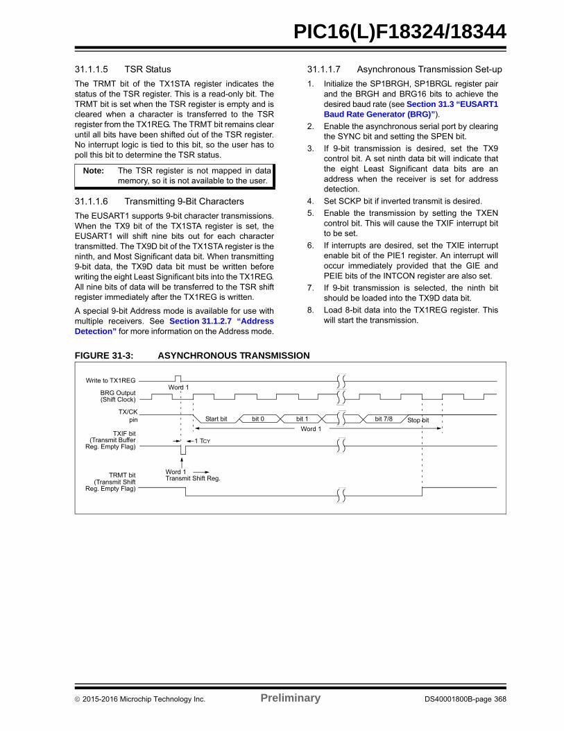
PIC16(L)F18324/18344
31.1.1.5 TSR Status
The TRMT bit of the TX1STA register indicates thestatus of the TSR register. This is a read-only bit. TheTRMT bit is set when the TSR register is empty and iscleared when a character is transferred to the TSRregister from the TX1REG. The TRMT bit remains clearuntil all bits have been shifted out of the TSR register.No interrupt logic is tied to this bit, so the user has topoll this bit to determine the TSR status.
31.1.1.6 Transmitting 9-Bit Characters
The EUSART1 supports 9-bit character transmissions.When the TX9 bit of the TX1STA register is set, theEUSART1 will shift nine bits out for each charactertransmitted. The TX9D bit of the TX1STA register is theninth, and Most Significant data bit. When transmitting9-bit data, the TX9D data bit must be written beforewriting the eight Least Significant bits into the TX1REG.All nine bits of data will be transferred to the TSR shiftregister immediately after the TX1REG is written.
A special 9-bit Address mode is available for use withmultiple receivers. See Section 31.1.2.7 “AddressDetection” for more information on the Address mode.
31.1.1.7 Asynchronous Transmission Set-up
1. Initialize the SP1BRGH, SP1BRGL register pairand the BRGH and BRG16 bits to achieve thedesired baud rate (see Section 31.3 “EUSART1Baud Rate Generator (BRG)”).
2. Enable the asynchronous serial port by clearingthe SYNC bit and setting the SPEN bit.
3. If 9-bit transmission is desired, set the TX9control bit. A set ninth data bit will indicate thatthe eight Least Significant data bits are anaddress when the receiver is set for addressdetection.
4. Set SCKP bit if inverted transmit is desired.
5. Enable the transmission by setting the TXENcontrol bit. This will cause the TXIF interrupt bitto be set.
6. If interrupts are desired, set the TXIE interruptenable bit of the PIE1 register. An interrupt willoccur immediately provided that the GIE andPEIE bits of the INTCON register are also set.
7. If 9-bit transmission is selected, the ninth bitshould be loaded into the TX9D data bit.
8. Load 8-bit data into the TX1REG register. Thiswill start the transmission.
FIGURE 31-3: ASYNCHRONOUS TRANSMISSION
Note: The TSR register is not mapped in datamemory, so it is not available to the user.
Word 1Stop bit
Word 1Transmit Shift Reg.
Start bit bit 0 bit 1 bit 7/8
Write to TX1REGWord 1
BRG Output(Shift Clock)
TX/CK
TXIF bit(Transmit Buffer
Reg. Empty Flag)
TRMT bit(Transmit Shift
Reg. Empty Flag)
1 TCY
pin
2015-2016 Microchip Technology Inc. Preliminary DS40001800B-page 368
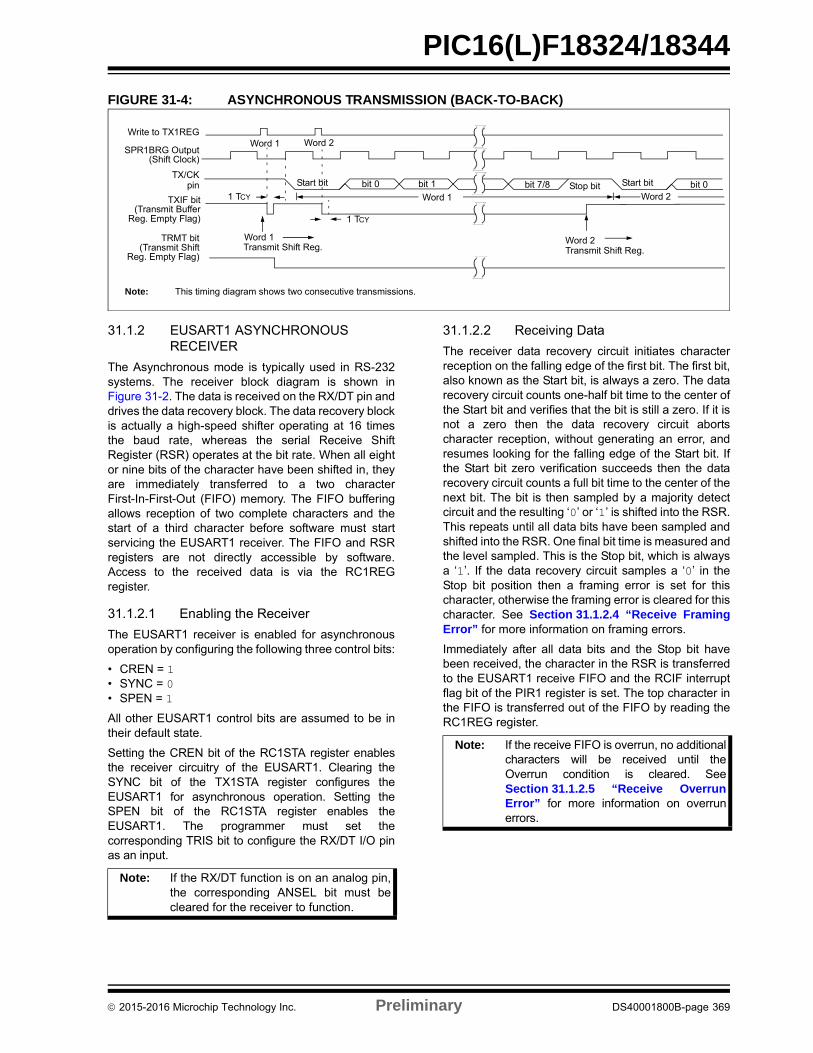
PIC16(L)F18324/18344
FIGURE 31-4: ASYNCHRONOUS TRANSMISSION (BACK-TO-BACK)
31.1.2 EUSART1 ASYNCHRONOUS RECEIVER
The Asynchronous mode is typically used in RS-232systems. The receiver block diagram is shown inFigure 31-2. The data is received on the RX/DT pin anddrives the data recovery block. The data recovery blockis actually a high-speed shifter operating at 16 timesthe baud rate, whereas the serial Receive ShiftRegister (RSR) operates at the bit rate. When all eightor nine bits of the character have been shifted in, theyare immediately transferred to a two characterFirst-In-First-Out (FIFO) memory. The FIFO bufferingallows reception of two complete characters and thestart of a third character before software must startservicing the EUSART1 receiver. The FIFO and RSRregisters are not directly accessible by software.Access to the received data is via the RC1REGregister.
31.1.2.1 Enabling the Receiver
The EUSART1 receiver is enabled for asynchronousoperation by configuring the following three control bits:
• CREN = 1• SYNC = 0• SPEN = 1
All other EUSART1 control bits are assumed to be intheir default state.
Setting the CREN bit of the RC1STA register enablesthe receiver circuitry of the EUSART1. Clearing theSYNC bit of the TX1STA register configures theEUSART1 for asynchronous operation. Setting theSPEN bit of the RC1STA register enables theEUSART1. The programmer must set thecorresponding TRIS bit to configure the RX/DT I/O pinas an input.
31.1.2.2 Receiving Data
The receiver data recovery circuit initiates characterreception on the falling edge of the first bit. The first bit,also known as the Start bit, is always a zero. The datarecovery circuit counts one-half bit time to the center ofthe Start bit and verifies that the bit is still a zero. If it isnot a zero then the data recovery circuit abortscharacter reception, without generating an error, andresumes looking for the falling edge of the Start bit. Ifthe Start bit zero verification succeeds then the datarecovery circuit counts a full bit time to the center of thenext bit. The bit is then sampled by a majority detectcircuit and the resulting ‘0’ or ‘1’ is shifted into the RSR.This repeats until all data bits have been sampled andshifted into the RSR. One final bit time is measured andthe level sampled. This is the Stop bit, which is alwaysa ‘1’. If the data recovery circuit samples a ‘0’ in theStop bit position then a framing error is set for thischaracter, otherwise the framing error is cleared for thischaracter. See Section 31.1.2.4 “Receive FramingError” for more information on framing errors.
Immediately after all data bits and the Stop bit havebeen received, the character in the RSR is transferredto the EUSART1 receive FIFO and the RCIF interruptflag bit of the PIR1 register is set. The top character inthe FIFO is transferred out of the FIFO by reading theRC1REG register.
Transmit Shift Reg.
Write to TX1REG
SPR1BRG Output(Shift Clock)
TX/CK
TRMT bit(Transmit Shift
Reg. Empty Flag)
Word 1 Word 2
Word 1 Word 2
Start bit Stop bit Start bit
Transmit Shift Reg.
Word 1 Word 2bit 0 bit 1 bit 7/8 bit 0
Note: This timing diagram shows two consecutive transmissions.
1 TCY
1 TCY
pin
TXIF bit(Transmit Buffer
Reg. Empty Flag)
Note: If the RX/DT function is on an analog pin,the corresponding ANSEL bit must becleared for the receiver to function.
Note: If the receive FIFO is overrun, no additionalcharacters will be received until theOverrun condition is cleared. SeeSection 31.1.2.5 “Receive OverrunError” for more information on overrunerrors.
2015-2016 Microchip Technology Inc. Preliminary DS40001800B-page 369
PIC16(L)F18324/18344
31.1.2.3 Receive Interrupts
The RCIF interrupt flag bit of the PIR1 register is setwhenever the EUSART1 receiver is enabled and thereis an unread character in the receive FIFO. The RCIFinterrupt flag bit is read-only, it cannot be set or clearedby software.
RCIF interrupts are enabled by setting all of thefollowing bits:
• RCIE, Interrupt Enable bit of the PIE1 register• PEIE, Peripheral Interrupt Enable bit of the
INTCON register• GIE, Global Interrupt Enable bit of the INTCON
register
The RCIF interrupt flag bit will be set when there is anunread character in the FIFO, regardless of the state ofinterrupt enable bits.
31.1.2.4 Receive Framing Error
Each character in the receive FIFO buffer has acorresponding framing error Status bit. A framing errorindicates that a Stop bit was not seen at the expectedtime. The framing error status is accessed via theFERR bit of the RC1STA register. The FERR bitrepresents the status of the top unread character in thereceive FIFO. Therefore, the FERR bit must be readbefore reading the RC1REG.
The FERR bit is read-only and only applies to the topunread character in the receive FIFO. A framing error(FERR = 1) does not preclude reception of additionalcharacters. It is not necessary to clear the FERR bit.Reading the next character from the FIFO buffer willadvance the FIFO to the next character and the nextcorresponding framing error.
The FERR bit can be forced clear by clearing the SPENbit of the RC1STA register which resets the EUSART1.Clearing the CREN bit of the RC1STA register does notaffect the FERR bit. A framing error by itself does notgenerate an interrupt.
31.1.2.5 Receive Overrun Error
The receive FIFO buffer can hold two characters. Anoverrun error will be generated if a third character, in itsentirety, is received before the FIFO is accessed. Whenthis happens the OERR bit of the RC1STA register isset. The characters already in the FIFO buffer can beread but no additional characters will be received untilthe error is cleared. The error must be cleared by eitherclearing the CREN bit of the RC1STA register or byresetting the EUSART1 by clearing the SPEN bit of theRC1STA register.
31.1.2.6 Receiving 9-Bit Characters
The EUSART1 supports 9-bit character reception.When the RX9 bit of the RC1STA register is set theEUSART1 will shift nine bits into the RSR for eachcharacter received. The RX9D bit of the RC1STA reg-ister is the ninth and Most Significant data bit of the topunread character in the receive FIFO. When reading9-bit data from the receive FIFO buffer, the RX9D databit must be read before reading the eight Least Signifi-cant bits from the RC1REG.
31.1.2.7 Address Detection
A special Address Detection mode is available for usewhen multiple receivers share the same transmissionline, such as in RS-485 systems. Address detection isenabled by setting the ADDEN bit of the RC1STAregister.
Address detection requires 9-bit character reception.When address detection is enabled, only characterswith the ninth data bit set will be transferred to thereceive FIFO buffer, thereby setting the RCIF interruptbit. All other characters will be ignored.
Upon receiving an address character, user softwaredetermines if the address matches its own. Uponaddress match, user software must disable addressdetection by clearing the ADDEN bit before the nextStop bit occurs. When user software detects the end ofthe message, determined by the message protocolused, software places the receiver back into theAddress Detection mode by setting the ADDEN bit.
Note: If all receive characters in the receiveFIFO have framing errors, repeated readsof the RC1REG will not clear the FERR bit.
2015-2016 Microchip Technology Inc. Preliminary DS40001800B-page 370
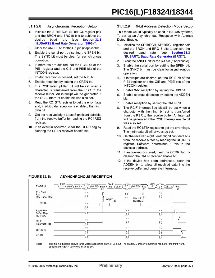
PIC16(L)F18324/18344
31.1.2.8 Asynchronous Reception Setup
1. Initialize the SP1BRGH, SP1BRGL register pairand the BRGH and BRG16 bits to achieve thedesired baud rate (see Section 31.3“EUSART1 Baud Rate Generator (BRG)”).
2. Clear the ANSEL bit for the RX pin (if applicable).
3. Enable the serial port by setting the SPEN bit.The SYNC bit must be clear for asynchronousoperation.
4. If interrupts are desired, set the RCIE bit of thePIE1 register and the GIE and PEIE bits of theINTCON register.
5. If 9-bit reception is desired, set the RX9 bit.
6. Enable reception by setting the CREN bit.
7. The RCIF interrupt flag bit will be set when acharacter is transferred from the RSR to thereceive buffer. An interrupt will be generated ifthe RCIE interrupt enable bit was also set.
8. Read the RC1STA register to get the error flagsand, if 9-bit data reception is enabled, the ninthdata bit.
9. Get the received eight Least Significant data bitsfrom the receive buffer by reading the RC1REGregister.
10. If an overrun occurred, clear the OERR flag byclearing the CREN receiver enable bit.
31.1.2.9 9-bit Address Detection Mode Setup
This mode would typically be used in RS-485 systems.To set up an Asynchronous Reception with AddressDetect Enable:
1. Initialize the SP1BRGH, SP1BRGL register pairand the BRGH and BRG16 bits to achieve thedesired baud rate (see Section 31.3“EUSART1 Baud Rate Generator (BRG)”).
2. Clear the ANSEL bit for the RX pin (if applicable).
3. Enable the serial port by setting the SPEN bit.The SYNC bit must be clear for asynchronousoperation.
4. If interrupts are desired, set the RCIE bit of thePIE1 register and the GIE and PEIE bits of theINTCON register.
5. Enable 9-bit reception by setting the RX9 bit.
6. Enable address detection by setting the ADDENbit.
7. Enable reception by setting the CREN bit.
8. The RCIF interrupt flag bit will be set when acharacter with the ninth bit set is transferredfrom the RSR to the receive buffer. An interruptwill be generated if the RCIE interrupt enable bitwas also set.
9. Read the RC1STA register to get the error flags.The ninth data bit will always be set.
10. Get the received eight Least Significant data bitsfrom the receive buffer by reading the RC1REGregister. Software determines if this is thedevice’s address.
11. If an overrun occurred, clear the OERR flag byclearing the CREN receiver enable bit.
12. If the device has been addressed, clear theADDEN bit to allow all received data into thereceive buffer and generate interrupts.
FIGURE 31-5: ASYNCHRONOUS RECEPTION
Startbit bit 7/8bit 1bit 0 bit 7/8 bit 0Stop
bit
Startbit
Startbitbit 7/8 Stop
bitRX/DT pin
RegRcv Buffer Reg.
Rcv Shift
Read RcvBuffer Reg.RC1REG
RCIF(Interrupt Flag)
OERR bit
CREN
Word 1RC1REG
Word 2RC1REG
Stopbit
Note: This timing diagram shows three words appearing on the RX input. The RC1REG (receive buffer) is read after the third word,causing the OERR (overrun) bit to be set.
RCIDL
2015-2016 Microchip Technology Inc. Preliminary DS40001800B-page 371
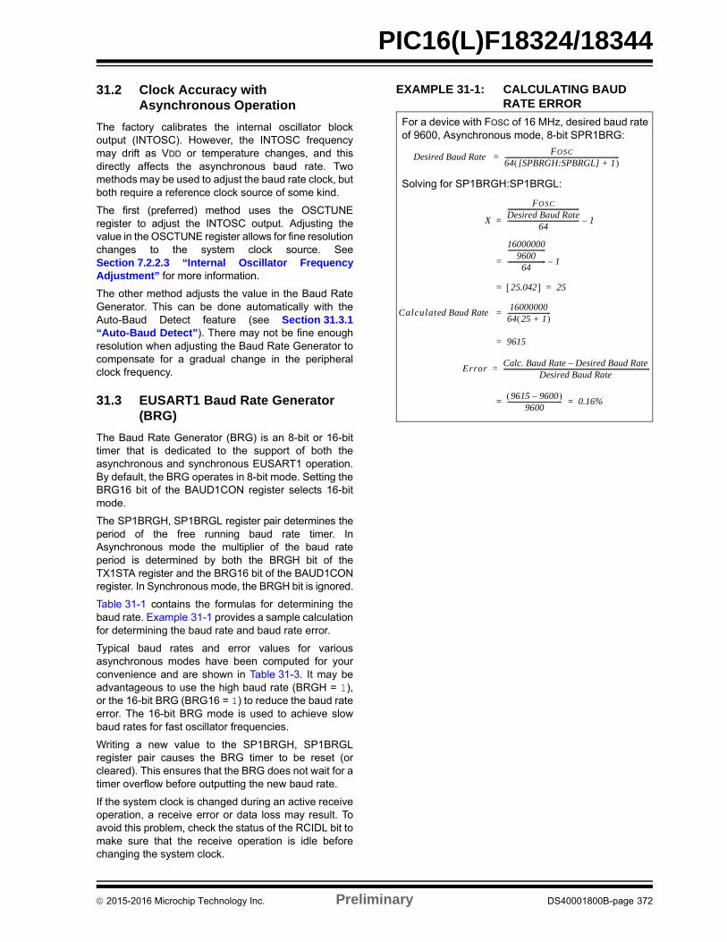
PIC16(L)F18324/18344
31.2 Clock Accuracy with Asynchronous Operation
The factory calibrates the internal oscillator blockoutput (INTOSC). However, the INTOSC frequencymay drift as VDD or temperature changes, and thisdirectly affects the asynchronous baud rate. Twomethods may be used to adjust the baud rate clock, butboth require a reference clock source of some kind.
The first (preferred) method uses the OSCTUNEregister to adjust the INTOSC output. Adjusting thevalue in the OSCTUNE register allows for fine resolutionchanges to the system clock source. SeeSection 7.2.2.3 “Internal Oscillator FrequencyAdjustment” for more information.
The other method adjusts the value in the Baud RateGenerator. This can be done automatically with theAuto-Baud Detect feature (see Section 31.3.1“Auto-Baud Detect”). There may not be fine enoughresolution when adjusting the Baud Rate Generator tocompensate for a gradual change in the peripheralclock frequency.
31.3 EUSART1 Baud Rate Generator (BRG)
The Baud Rate Generator (BRG) is an 8-bit or 16-bittimer that is dedicated to the support of both theasynchronous and synchronous EUSART1 operation.By default, the BRG operates in 8-bit mode. Setting theBRG16 bit of the BAUD1CON register selects 16-bitmode.
The SP1BRGH, SP1BRGL register pair determines theperiod of the free running baud rate timer. InAsynchronous mode the multiplier of the baud rateperiod is determined by both the BRGH bit of theTX1STA register and the BRG16 bit of the BAUD1CONregister. In Synchronous mode, the BRGH bit is ignored.
Table 31-1 contains the formulas for determining thebaud rate. Example 31-1 provides a sample calculationfor determining the baud rate and baud rate error.
Typical baud rates and error values for variousasynchronous modes have been computed for yourconvenience and are shown in Table 31-3. It may beadvantageous to use the high baud rate (BRGH = 1),or the 16-bit BRG (BRG16 = 1) to reduce the baud rateerror. The 16-bit BRG mode is used to achieve slowbaud rates for fast oscillator frequencies.
Writing a new value to the SP1BRGH, SP1BRGLregister pair causes the BRG timer to be reset (orcleared). This ensures that the BRG does not wait for atimer overflow before outputting the new baud rate.
If the system clock is changed during an active receiveoperation, a receive error or data loss may result. Toavoid this problem, check the status of the RCIDL bit tomake sure that the receive operation is idle beforechanging the system clock.
EXAMPLE 31-1: CALCULATING BAUD RATE ERROR
For a device with FOSC of 16 MHz, desired baud rateof 9600, Asynchronous mode, 8-bit SPR1BRG:
Solving for SP1BRGH:SP1BRGL:
X
FOSC
Desired Baud Rate---------------------------------------------
64--------------------------------------------- 1–=
Desired Baud Rate FOSC
64 [SPBRGH:SPBRGL] 1+ ------------------------------------------------------------------------=
160000009600
------------------------
64------------------------ 1–=
25.042 25= =
Calculated Baud Rate 16000000
64 25 1+ ---------------------------=
9615=
ErrorCalc. Baud Rate Desired Baud Rate –
Desired Baud Rate --------------------------------------------------------------------------------------------=
9615 9600–
9600---------------------------------- 0.16%= =
2015-2016 Microchip Technology Inc. Preliminary DS40001800B-page 372
PIC16(L)F18324/18344
31.3.1 AUTO-BAUD DETECT
The EUSART1 module supports automatic detectionand calibration of the baud rate.
In the Auto-Baud Detect (ABD) mode, the clock to theBRG is reversed. Rather than the BRG clocking theincoming RX signal, the RX signal is timing the BRG.The Baud Rate Generator is used to time the period ofa received 55h (ASCII “U”) which is the Sync characterfor the LIN bus. The unique feature of this character isthat it has five rising edges including the Stop bit edge.
Setting the ABDEN bit of the BAUD1CON registerstarts the auto-baud calibration sequence. While theABD sequence takes place, the EUSART1 statemachine is held in Idle. On the first rising edge of thereceive line, after the Start bit, the SPBRG beginscounting up using the BRG counter clock as shown inFigure 31-6. The fifth rising edge will occur on the RXpin at the end of the eighth bit period. At that time, anaccumulated value totaling the proper BRG period isleft in the SP1BRGH, SP1BRGL register pair, theABDEN bit is automatically cleared and the RCIFinterrupt flag is set. The value in the RC1REG needs tobe read to clear the RCIF interrupt. RC1REG contentshould be discarded. When calibrating for modes thatdo not use the SP1BRGH register the user can verifythat the SP1BRGL register did not overflow bychecking for 00h in the SP1BRGH register.
The BRG auto-baud clock is determined by the BRG16and BRGH bits as shown in Table 31-1. During ABD,both the SP1BRGH and SP1BRGL registers are usedas a 16-bit counter, independent of the BRG16 bitsetting. While calibrating the baud rate period, theSP1BRGH and SP1BRGL registers are clocked at1/8th the BRG base clock rate.
The resulting byte measurement is the average bit timewhen clocked at full speed.
FIGURE 31-6: AUTOMATIC BAUD RATE CALIBRATION
Note 1: If the WUE bit is set with the ABDEN bit,auto-baud detection will occur on the bytefollowing the Break character (seeSection 31.3.3 “Auto-Wake-up onBreak”).
2: It is up to the user to determine that theincoming character baud rate is within therange of the selected BRG clock source.Some combinations of oscillator frequencyand EUSART1 baud rates are not possible.
3: During the auto-baud process, theauto-baud counter starts counting at one.Upon completion of the auto-baudsequence, to achieve maximum accuracy,subtract 1 from the SP1BRGH:SP1BRGLregister pair.
TABLE 31-1: BRG COUNTER CLOCK RATES
BRG16 BRGHBRG Base
ClockBRG ABD
Clock
0 0 FOSC/64 FOSC/512
0 1 FOSC/16 FOSC/128
1 0 FOSC/16 FOSC/128
1 1 FOSC/4 FOSC/32
Note: During the ABD sequence, SP1BRGL andSP1BRGH registers are both used as a16-bit counter, independent of the BRG16setting.
SPR1BRG Value
RX pin
ABDEN bit
RCIF bit
bit 0 bit 1
(Interrupt)
ReadRC1REG
SPR1BRG Clock
Start
Auto ClearedSet by User
XXXXh 0000h
Edge #1
bit 2 bit 3Edge #2
bit 4 bit 5Edge #3
bit 6 bit 7Edge #4
Stop bit
Edge #5
001Ch
Note 1: The ABD sequence requires the EUSART module to be configured in Asynchronous mode.
SP1BRGL XXh 1Ch
SP1BRGH XXh 00h
RCIDL
2015-2016 Microchip Technology Inc. Preliminary DS40001800B-page 373
PIC16(L)F18324/18344
31.3.2 AUTO-BAUD OVERFLOW
During the course of automatic-baud detection, theABDOVF bit of the BAUD1CON register will be set ifthe baud rate counter overflows before the fifth risingedge is detected on the RX pin. The ABDOVF bitindicates that the counter has exceeded the maximumcount that can fit in the 16 bits of theSP1BRGH:SP1BRGL register pair. The Overflowcondition will set the RCIF flag. The counter continuesto count until the fifth rising edge is detected on the RXpin. The RCIDL bit will remain false (‘0’) until the fifthrising edge at which time the RCIDL bit will be set. If theRC1REG is read after the overflow occurs but beforethe fifth rising edge, then the fifth rising edge will set theRCIF again.
Terminating the auto-baud process early to clear anOverflow condition will prevent proper detection of thesync character fifth rising edge. If any falling edges ofthe sync character have not yet occurred when theABDEN bit is cleared, then those will be falselydetected as Start bits. The following steps arerecommended to clear the Overflow condition:
1. Read RC1REG to clear RCIF
2. If RCIDL is zero, then wait for RCIF and repeatstep 1
3. Clear the ABDOVF bit
31.3.3 AUTO-WAKE-UP ON BREAK
During Sleep mode, all clocks to the EUSART1 aresuspended. Because of this, the Baud Rate Generatoris inactive and a proper character reception cannot beperformed. The Auto-Wake-up feature allows thecontroller to wake-up due to activity on the RX/DT line.This feature is available only in Asynchronous mode.
The Auto-Wake-up feature is enabled by setting theWUE bit of the BAUD1CON register. Once set, thenormal receive sequence on RX/DT is disabled, and theEUSART1 remains in an Idle state, monitoring for awake-up event independent of the CPU mode. Awake-up event consists of a high-to-low transition on theRX/DT line. (This coincides with the start of a Sync Breakor a wake-up signal character for the LIN protocol.)
The EUSART1 module generates an RCIF interruptcoincident with the wake-up event. The interrupt isgenerated synchronously to the Q clocks in normal CPUoperating modes (Figure 31-7), and asynchronously ifthe device is in Sleep mode (Figure 31-8). The Interruptcondition is cleared by reading the RC1REG register.
The WUE bit is automatically cleared by the low-to-hightransition on the RX line at the end of the Break. Thissignals to the user that the Break event is over. At thispoint, the EUSART1 module is in Idle mode waiting toreceive the next character.
31.3.3.1 Special Considerations
Break Character
To avoid character errors or character fragments duringa wake-up event, the wake-up character must be allzeros.
When the wake-up is enabled the function worksindependent of the low time on the data stream. If theWUE bit is set and a valid non-zero character isreceived, the low time from the Start bit to the first risingedge will be interpreted as the wake-up event. Theremaining bits in the character will be received as afragmented character and subsequent characters canresult in framing or overrun errors.
Therefore, the initial character in the transmission mustbe all ‘0’s. This must be ten or more bit times, 13-bittimes recommended for LIN bus, or any number of bittimes for standard RS-232 devices.
Oscillator Start-up Time
Oscillator start-up time must be considered, especiallyin applications using oscillators with longer start-upintervals (i.e., LP, XT or HS/PLL mode). The SyncBreak (or wake-up signal) character must be ofsufficient length, and be followed by a sufficientinterval, to allow enough time for the selected oscillatorto start and provide proper initialization of theEUSART1.
WUE Bit
The wake-up event causes a receive interrupt bysetting the RCIF bit. The WUE bit is cleared inhardware by a rising edge on RX/DT. The Interruptcondition is then cleared in software by reading theRC1REG register and discarding its contents.
To ensure that no actual data is lost, check the RCIDLbit to verify that a receive operation is not in processbefore setting the WUE bit. If a receive operation is notoccurring, the WUE bit may then be set just prior toentering the Sleep mode.
2015-2016 Microchip Technology Inc. Preliminary DS40001800B-page 374
PIC16(L)F18324/18344
FIGURE 31-7: AUTO-WAKE-UP BIT (WUE) TIMING DURING NORMAL OPERATION
FIGURE 31-8: AUTO-WAKE-UP BIT (WUE) TIMINGS DURING SLEEP
31.3.4 BREAK CHARACTER SEQUENCE
The EUSART1 module has the capability of sendingthe special Break character sequences that arerequired by the LIN bus standard. A Break characterconsists of a Start bit, followed by 12 ‘0’ bits and a Stopbit.
To send a Break character, set the SENDB and TXENbits of the TX1STA register. The Break charactertransmission is then initiated by a write to the TX1REG.The value of data written to TX1REG will be ignoredand all ‘0’s will be transmitted.
The SENDB bit is automatically reset by hardware afterthe corresponding Stop bit is sent. This allows the userto preload the transmit FIFO with the next transmit bytefollowing the Break character (typically, the Synccharacter in the LIN specification).
The TRMT bit of the TX1STA register indicates when thetransmit operation is active or idle, just as it does duringnormal transmission. See Figure 31-9 for the timing ofthe Break character sequence.
31.3.4.1 Break and Sync Transmit Sequence
The following sequence will start a message frameheader made up of a Break, followed by an auto-baudSync byte. This sequence is typical of a LIN busmaster.
1. Configure the EUSART1 for the desired mode.
2. Set the TXEN and SENDB bits to enable theBreak sequence.
3. Load the TX1REG with a dummy character toinitiate transmission (the value is ignored).
4. Write ‘55h’ to TX1REG to load the Synccharacter into the transmit FIFO buffer.
5. After the Break has been sent, the SENDB bit isreset by hardware and the Sync character isthen transmitted.
When the TX1REG becomes empty, as indicated bythe TXIF, the next data byte can be written to TX1REG.
Q1 Q2 Q3 Q4 Q1 Q2 Q3Q4 Q1Q2 Q3 Q4 Q1Q2 Q3 Q4 Q1Q2 Q3 Q4 Q1Q2 Q3 Q4 Q1 Q2 Q3 Q4 Q1Q2 Q3 Q4 Q1 Q2 Q3 Q4 Q1Q2 Q3 Q4
OSC1
WUE bit
RX/DT Line
RCIF
Bit set by user Auto Cleared
Cleared due to User Read of RC1REG
Note 1: The EUSART remains in Idle while the WUE bit is set.
Q1Q2Q3 Q4 Q1Q2 Q3 Q4 Q1Q2 Q3 Q4 Q1 Q2 Q3 Q4 Q1Q2 Q3 Q4 Q1Q2 Q3 Q4 Q1 Q2Q3 Q4 Q1Q2 Q3 Q4
OSC1
WUE bit
RX/DT Line
RCIF
Bit Set by User Auto Cleared
Cleared due to User Read of RC1REGSleep Command Executed
Note 1
Note 1: If the wake-up event requires long oscillator warm-up time, the automatic clearing of the WUE bit can occur while the stposc signal isstill active. This sequence should not depend on the presence of Q clocks.
2: The EUSART remains in Idle while the WUE bit is set.
Sleep Ends
2015-2016 Microchip Technology Inc. Preliminary DS40001800B-page 375
PIC16(L)F18324/18344
31.3.5 RECEIVING A BREAK CHARACTER
The EUSART1 module can receive a Break characterin two ways.
The first method to detect a Break character uses theFERR bit of the RC1STA register and the received dataas indicated by RC1REG. The Baud Rate Generator isassumed to have been initialized to the expected baudrate.
A Break character has been received when;
• RCIF bit is set• FERR bit is set• RC1REG = 00h
The second method uses the Auto-Wake-up featuredescribed in Section 31.3.3 “Auto-Wake-up onBreak”. By enabling this feature, the EUSART1 willsample the next two transitions on RX/DT, cause anRCIF interrupt, and receive the next data byte followedby another interrupt.
Note that following a Break character, the user willtypically want to enable the Auto-Baud Detect feature.For both methods, the user can set the ABDEN bit ofthe BAUD1CON register before placing the EUSART1in Sleep mode.
FIGURE 31-9: SEND BREAK CHARACTER SEQUENCE
Write to TX1REGDummy Write
SPR1BRG Output(Shift Clock)
Start bit bit 0 bit 1 bit 11 Stop bit
Break
TXIF bit(Transmit
Interrupt Flag)
TX (pin)
TRMT bit(Transmit Shift
Empty Flag)
SENDB(send Break
control bit)
SENDB Sampled Here Auto Cleared
2015-2016 Microchip Technology Inc. Preliminary DS40001800B-page 376
PIC16(L)F18324/18344
31.4 EUSART1 Synchronous Mode
Synchronous serial communications are typically usedin systems with a single master and one or moreslaves. The master device contains the necessarycircuitry for baud rate generation and supplies the clockfor all devices in the system. Slave devices can takeadvantage of the master clock by eliminating theinternal clock generation circuitry.
There are two signal lines in Synchronous mode: abidirectional data line and a clock line. Slaves use theexternal clock supplied by the master to shift the serialdata into and out of their respective receive and trans-mit shift registers. Since the data line is bidirectional,synchronous operation is half-duplex only. Half-duplexrefers to the fact that master and slave devices canreceive and transmit data but not both simultaneously.The EUSART1 can operate as either a master or slavedevice.
Start and Stop bits are not used in synchronoustransmissions.
31.4.1 SYNCHRONOUS MASTER MODE
The following bits are used to configure the EUSART1for synchronous master operation:
• SYNC = 1
• CSRC = 1
• SREN = 0 (for transmit); SREN = 1 (for receive)
• CREN = 0 (for transmit); CREN = 1 (for receive)
• SPEN = 1
Setting the SYNC bit of the TX1STA register configuresthe device for synchronous operation. Setting the CSRCbit of the TX1STA register configures the device as amaster. Clearing the SREN and CREN bits of theRC1STA register ensures that the device is in theTransmit mode, otherwise the device will be configuredto receive. Setting the SPEN bit of the RC1STA registerenables the EUSART1.
31.4.1.1 Master Clock
Synchronous data transfers use a separate clock line,which is synchronous with the data. A deviceconfigured as a master transmits the clock on theTX/CK line. The TX/CK pin output driver isautomatically enabled when the EUSART1 isconfigured for synchronous transmit or receiveoperation. Serial data bits change on the leading edgeto ensure they are valid at the trailing edge of eachclock. One clock cycle is generated for each data bit.Only as many clock cycles are generated as there aredata bits.
31.4.1.2 Clock Polarity
A clock polarity option is provided for Microwirecompatibility. Clock polarity is selected with the SCKPbit of the BAUD1CON register. Setting the SCKP bitsets the clock Idle state as high. When the SCKP bit isset, the data changes on the falling edge of each clock.Clearing the SCKP bit sets the Idle state as low. Whenthe SCKP bit is cleared, the data changes on the risingedge of each clock.
31.4.1.3 Synchronous Master Transmission
Data is transferred out of the device on the RX/DT pin.The RX/DT and TX/CK pin output drivers are automat-ically enabled when the EUSART1 is configured forsynchronous master transmit operation.
A transmission is initiated by writing a character to theTX1REG register. If the TSR still contains all or part ofa previous character the new character data is held inthe TX1REG until the last bit of the previous characterhas been transmitted. If this is the first character, or theprevious character has been completely flushed fromthe TSR, the data in the TX1REG is immediately trans-ferred to the TSR. The transmission of the charactercommences immediately following the transfer of thedata to the TSR from the TX1REG.
Each data bit changes on the leading edge of themaster clock and remains valid until the subsequentleading clock edge.
31.4.1.4 Synchronous Master Transmission Set-up
1. Initialize the SP1BRGH, SP1BRGL register pairand the BRGH and BRG16 bits to achieve thedesired baud rate (see Section 31.3“EUSART1 Baud Rate Generator (BRG)”).
2. Enable the synchronous master serial port bysetting bits SYNC, SPEN and CSRC.
3. Disable Receive mode by clearing bits SRENand CREN.
4. Enable Transmit mode by setting the TXEN bit.
5. If 9-bit transmission is desired, set the TX9 bit.
6. If interrupts are desired, set the TXIE bit of thePIE1 register and the GIE and PEIE bits of theINTCON register.
7. If 9-bit transmission is selected, the ninth bitshould be loaded in the TX9D bit.
8. Start transmission by loading data to theTX1REG register.
Note: The TSR register is not mapped in datamemory, so it is not available to the user.
2015-2016 Microchip Technology Inc. Preliminary DS40001800B-page 377
PIC16(L)F18324/18344
FIGURE 31-10: SYNCHRONOUS TRANSMISSION
FIGURE 31-11: SYNCHRONOUS TRANSMISSION (THROUGH TXEN)
31.4.1.5 Synchronous Master Reception
Data is received at the RX/DT pin. The RX/DT pinoutput driver is automatically disabled when theEUSART1 is configured for synchronous masterreceive operation.
In Synchronous mode, reception is enabled by settingeither the Single Receive Enable bit (SREN of theRC1STA register) or the Continuous Receive Enablebit (CREN of the RC1STA register).
When SREN is set and CREN is clear, only as manyclock cycles are generated as there are data bits in asingle character. The SREN bit is automatically clearedat the completion of one character. When CREN is set,clocks are continuously generated until CREN iscleared. If CREN is cleared in the middle of a characterthe CK clock stops immediately and the partial charac-ter is discarded. If SREN and CREN are both set, thenSREN is cleared at the completion of the first characterand CREN takes precedence.
To initiate reception, set either SREN or CREN. Data issampled at the RX/DT pin on the trailing edge of theTX/CK clock pin and is shifted into the Receive ShiftRegister (RSR). When a complete character isreceived into the RSR, the RCIF bit is set and thecharacter is automatically transferred to the twocharacter receive FIFO. The Least Significant eight bitsof the top character in the receive FIFO are available inRC1REG. The RCIF bit remains set as long as thereare unread characters in the receive FIFO.
bit 0 bit 1 bit 7
Word 1
bit 2 bit 0 bit 1 bit 7RX/DT
Write toTX1REG Reg
TXIF bit(Interrupt Flag)
TXEN bit‘1’ ‘1’
Word 2
TRMT bit
Write Word 1 Write Word 2
Note: Sync Master mode, SP1BRGL = 0, continuous transmission of two 8-bit words.
pin
TX/CK pin
TX/CK pin
(SCKP = 0)
(SCKP = 1)
RX/DT pin
TX/CK pin
Write toTX1REG reg
TXIF bit
TRMT bit
bit 0 bit 1 bit 2 bit 6 bit 7
TXEN bit
Note: If the RX/DT function is on an analog pin,the corresponding ANSEL bit must becleared for the receiver to function.
2015-2016 Microchip Technology Inc. Preliminary DS40001800B-page 378
PIC16(L)F18324/18344
31.4.1.6 Slave Clock
Synchronous data transfers use a separate clock line,which is synchronous with the data. A device configuredas a slave receives the clock on the TX/CK line. TheTX/CK pin output driver is automatically disabled whenthe device is configured for synchronous slave transmitor receive operation. Serial data bits change on theleading edge to ensure they are valid at the trailing edgeof each clock. One data bit is transferred for each clockcycle. Only as many clock cycles should be received asthere are data bits.
31.4.1.7 Receive Overrun Error
The receive FIFO buffer can hold two characters. Anoverrun error will be generated if a third character, in itsentirety, is received before RC1REG is read to accessthe FIFO. When this happens the OERR bit of theRC1STA register is set. Previous data in the FIFO willnot be overwritten. The two characters in the FIFObuffer can be read, however, no additional characterswill be received until the error is cleared. The OERR bitcan only be cleared by clearing the Overrun condition.If the overrun error occurred when the SREN bit is setand CREN is clear then the error is cleared by readingRC1REG. If the overrun occurred when the CREN bit isset then the Error condition is cleared by either clearingthe CREN bit of the RC1STA register or by clearing theSPEN bit which resets the EUSART1.
31.4.1.8 Receiving 9-bit Characters
The EUSART1 supports 9-bit character reception.When the RX9 bit of the RC1STA register is set theEUSART1 will shift nine bits into the RSR for eachcharacter received.
The RX9D bit of the RC1STA register is the ninth, andMost Significant, data bit of the top unread character inthe receive FIFO. When reading 9-bit data from thereceive FIFO buffer, the RX9D data bit must be readbefore reading the eight Least Significant bits from theRC1REG.
31.4.1.9 Synchronous Master Reception Set-up
1. Initialize the SP1BRGH, SP1BRGL register pairfor the appropriate baud rate. Set or clear theBRGH and BRG16 bits, as required, to achievethe desired baud rate.
2. Clear the ANSEL bit for the RX pin (if applicable).
3. Enable the synchronous master serial port bysetting bits SYNC, SPEN and CSRC.
4. Ensure bits CREN and SREN are clear.
5. If interrupts are desired, set the RCIE bit of thePIE1 register and the GIE and PEIE bits of theINTCON register.
6. If 9-bit reception is desired, set bit RX9.
7. Start reception by setting the SREN bit or forcontinuous reception, set the CREN bit.
8. Interrupt flag bit RCIF will be set when receptionof a character is complete. An interrupt will begenerated if the enable bit RCIE was set.
9. Read the RC1STA register to get the ninth bit (ifenabled) and determine if any error occurredduring reception.
10. Read the 8-bit received data by reading theRC1REG register.
11. If an overrun error occurs, clear the error byeither clearing the CREN bit of the RC1STAregister or by clearing the SPEN bit which resetsthe EUSART1.
FIGURE 31-12: SYNCHRONOUS RECEPTION (MASTER MODE, SREN)
Note: If the device is configured as a slave andthe TX/CK function is on an analog pin, thecorresponding ANSEL bit must be cleared.
CREN bit
RX/DT
Write tobit SREN
SREN bit
RCIF bit(Interrupt)
ReadRC1REG
‘0’
bit 0 bit 1 bit 2 bit 3 bit 4 bit 5 bit 6 bit 7
‘0’
Note: Timing diagram demonstrates Sync Master mode with bit SREN = 1 and bit BRGH = 0.
TX/CK pin
TX/CK pin
pin
(SCKP = 0)
(SCKP = 1)
2015-2016 Microchip Technology Inc. Preliminary DS40001800B-page 379
PIC16(L)F18324/18344
31.4.2 SYNCHRONOUS SLAVE MODE
The following bits are used to configure the EUSART1for synchronous slave operation:
• SYNC = 1• CSRC = 0• SREN = 0 (for transmit); SREN = 1 (for receive)• CREN = 0 (for transmit); CREN = 1 (for receive)• SPEN = 1
Setting the SYNC bit of the TX1STA register configuresthe device for synchronous operation. Clearing theCSRC bit of the TX1STA register configures the deviceas a slave. Clearing the SREN and CREN bits of theRC1STA register ensures that the device is in theTransmit mode, otherwise the device will be configured toreceive. Setting the SPEN bit of the RC1STA registerenables the EUSART1.
31.4.2.1 EUSART1 Synchronous Slave Transmit
The operation of the Synchronous Master and Slavemodes are identical (see Section 31.4.1.3“Synchronous Master Transmission”), except in thecase of the Sleep mode.
If two words are written to the TX1REG and then theSLEEP instruction is executed, the following will occur:
1. The first character will immediately transfer tothe TSR register and transmit.
2. The second word will remain in the TX1REGregister.
3. The TXIF bit will not be set.
4. After the first character has been shifted out ofTSR, the TX1REG register will transfer thesecond character to the TSR and the TXIF bit willnow be set.
5. If the PEIE and TXIE bits are set, the interruptwill wake the device from Sleep and execute thenext instruction. If the GIE bit is also set, theprogram will call the Interrupt Service Routine.
31.4.2.2 Synchronous Slave Transmission Set-up
1. Set the SYNC and SPEN bits and clear theCSRC bit.
2. Clear the ANSEL bit for the CK pin (if applicable).
3. Clear the CREN and SREN bits.
4. If interrupts are desired, set the TXIE bit of thePIE1 register and the GIE and PEIE bits of theINTCON register.
5. If 9-bit transmission is desired, set the TX9 bit.
6. Enable transmission by setting the TXEN bit.
7. If 9-bit transmission is selected, insert the MostSignificant bit into the TX9D bit.
8. Start transmission by writing the LeastSignificant eight bits to the TX1REG register.
31.4.2.3 EUSART1 Synchronous Slave Reception
The operation of the Synchronous Master and Slavemodes is identical (Section 31.4.1.5 “SynchronousMaster Reception”), with the following exceptions:
• Sleep• CREN bit is always set, therefore the receiver is
never idle• SREN bit, which is a “don’t care” in Slave mode
A character may be received while in Sleep mode bysetting the CREN bit prior to entering Sleep. Once theword is received, the RSR register will transfer the datato the RC1REG register. If the RCIE enable bit is set,the interrupt generated will wake the device from Sleepand execute the next instruction. If the GIE bit is alsoset, the program will branch to the interrupt vector.
31.4.2.4 Synchronous Slave Reception Set-up
1. Set the SYNC and SPEN bits and clear theCSRC bit.
2. Clear the ANSEL bit for both the CK and DT pins(if applicable).
3. If interrupts are desired, set the RCIE bit of thePIE1 register and the GIE and PEIE bits of theINTCON register.
4. If 9-bit reception is desired, set the RX9 bit.
5. Set the CREN bit to enable reception.
6. The RCIF bit will be set when reception iscomplete. An interrupt will be generated if theRCIE bit was set.
7. If 9-bit mode is enabled, retrieve the MostSignificant bit from the RX9D bit of the RC1STAregister.
8. Retrieve the eight Least Significant bits from thereceive FIFO by reading the RC1REG register.
9. If an overrun error occurs, clear the error byeither clearing the CREN bit of the RC1STAregister or by clearing the SPEN bit which resetsthe EUSART1.
2015-2016 Microchip Technology Inc. Preliminary DS40001800B-page 380
PIC16(L)F18324/18344
31.5 EUSART1 Operation During Sleep
The EUSART1 will remain active during Sleep only inthe Synchronous Slave mode. All other modes requirethe system clock and therefore cannot generate thenecessary signals to run the Transmit or Receive Shiftregisters during Sleep.
Synchronous Slave mode uses an externally generatedclock to run the Transmit and Receive Shift registers.
31.5.1 SYNCHRONOUS RECEIVE DURING SLEEP
To receive during Sleep, all the following conditionsmust be met before entering Sleep mode:
• RC1STA and TX1STA Control registers must be configured for Synchronous Slave Reception (see Section 31.4.2.4 “Synchronous Slave Recep-tion Set-up”).
• If interrupts are desired, set the RCIE bit of the PIE1 register and the GIE and PEIE bits of the INTCON register.
• The RCIF interrupt flag must be cleared by read-ing RC1REG to unload any pending characters in the receive buffer.
Upon entering Sleep mode, the device will be ready toaccept data and clocks on the RX/DT and TX/CK pins,respectively. When the data word has been completelyclocked in by the external device, the RCIF interruptflag bit of the PIR1 register will be set. Thereby, wakingthe processor from Sleep.
Upon waking from Sleep, the instruction following theSLEEP instruction will be executed. If the GlobalInterrupt Enable (GIE) bit of the INTCON register isalso set, then the Interrupt Service Routine at address004h will be called.
31.5.2 SYNCHRONOUS TRANSMIT DURING SLEEP
To transmit during Sleep, all the following conditionsmust be met before entering Sleep mode:
• The RC1STA and TX1STA Control registers must be configured for synchronous slave transmission (see Section 31.4.2.2 “Synchronous Slave Transmission Set-up”).
• The TXIF interrupt flag must be cleared by writing the output data to the TX1REG, thereby filling the TSR and transmit buffer.
• If interrupts are desired, set the TXIE bit of the PIE1 register and the PEIE bit of the INTCON register.
• Interrupt enable bits TXIE of the PIE1 register and PEIE of the INTCON register must set.
Upon entering Sleep mode, the device will be ready toaccept clocks on TX/CK pin and transmit data on theRX/DT pin. When the data word in the TSR has beencompletely clocked out by the external device, thepending byte in the TX1REG will transfer to the TSRand the TXIF flag will be set. Thereby, waking the pro-cessor from Sleep. At this point, the TX1REG is avail-able to accept another character for transmission,which will clear the TXIF flag.
Upon waking from Sleep, the instruction following theSLEEP instruction will be executed. If the GlobalInterrupt Enable (GIE) bit is also set then the InterruptService Routine at address 0004h will be called.
2015-2016 Microchip Technology Inc. Preliminary DS40001800B-page 381
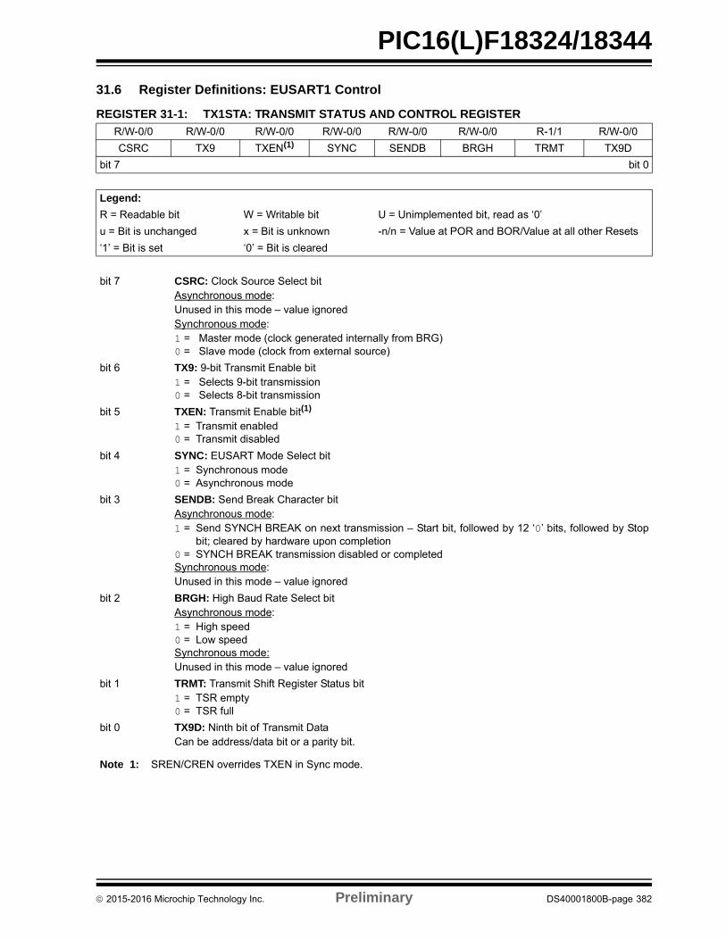
PIC16(L)F18324/18344
31.6 Register Definitions: EUSART1 Control
REGISTER 31-1: TX1STA: TRANSMIT STATUS AND CONTROL REGISTER
R/W-0/0 R/W-0/0 R/W-0/0 R/W-0/0 R/W-0/0 R/W-0/0 R-1/1 R/W-0/0
CSRC TX9 TXEN(1) SYNC SENDB BRGH TRMT TX9D
bit 7 bit 0
Legend:
R = Readable bit W = Writable bit U = Unimplemented bit, read as ‘0’
u = Bit is unchanged x = Bit is unknown -n/n = Value at POR and BOR/Value at all other Resets
‘1’ = Bit is set ‘0’ = Bit is cleared
bit 7 CSRC: Clock Source Select bitAsynchronous mode: Unused in this mode – value ignoredSynchronous mode: 1 = Master mode (clock generated internally from BRG)0 = Slave mode (clock from external source)
bit 6 TX9: 9-bit Transmit Enable bit1 = Selects 9-bit transmission0 = Selects 8-bit transmission
bit 5 TXEN: Transmit Enable bit(1)
1 = Transmit enabled0 = Transmit disabled
bit 4 SYNC: EUSART Mode Select bit 1 = Synchronous mode 0 = Asynchronous mode
bit 3 SENDB: Send Break Character bitAsynchronous mode:1 = Send SYNCH BREAK on next transmission – Start bit, followed by 12 ‘0’ bits, followed by Stop
bit; cleared by hardware upon completion0 = SYNCH BREAK transmission disabled or completedSynchronous mode:Unused in this mode – value ignored
bit 2 BRGH: High Baud Rate Select bitAsynchronous mode: 1 = High speed 0 = Low speedSynchronous mode: Unused in this mode – value ignored
bit 1 TRMT: Transmit Shift Register Status bit1 = TSR empty 0 = TSR full
bit 0 TX9D: Ninth bit of Transmit DataCan be address/data bit or a parity bit.
Note 1: SREN/CREN overrides TXEN in Sync mode.
2015-2016 Microchip Technology Inc. Preliminary DS40001800B-page 382
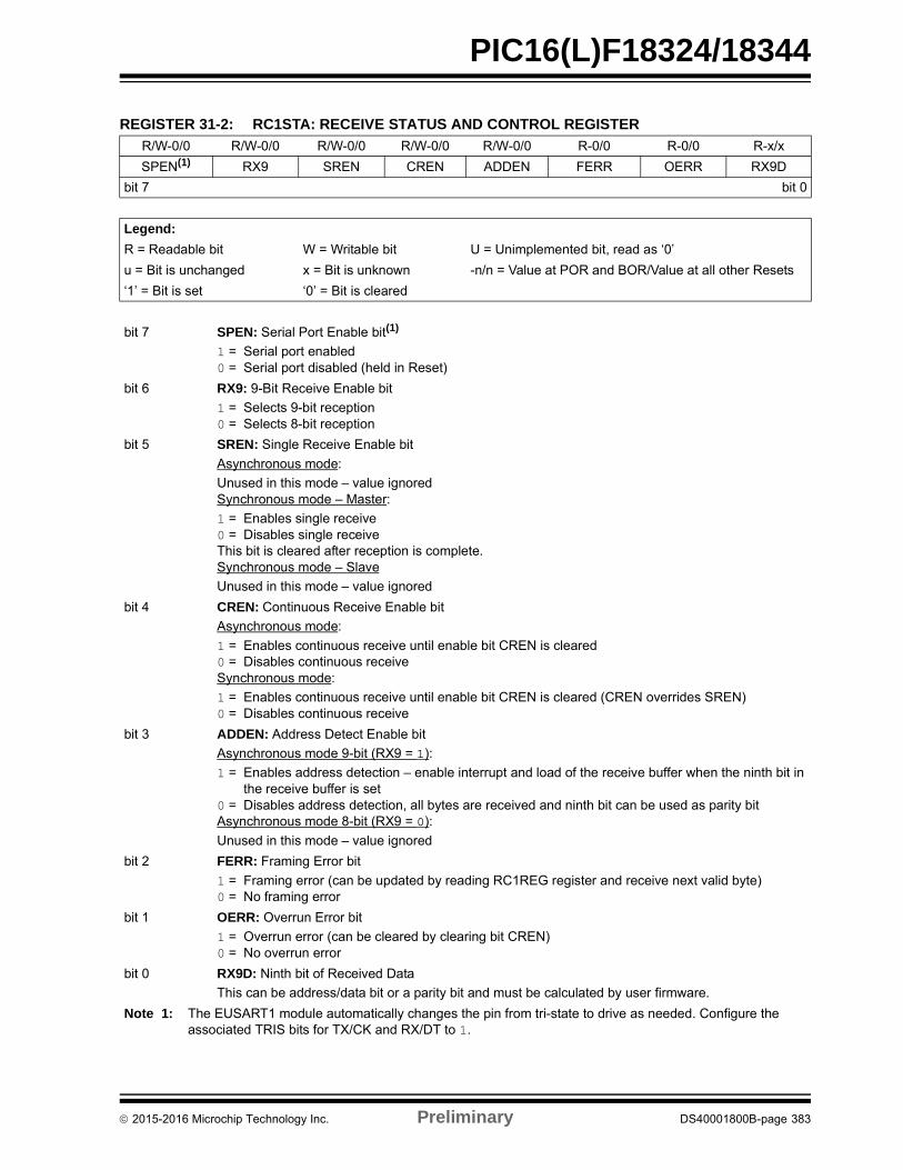
PIC16(L)F18324/18344
REGISTER 31-2: RC1STA: RECEIVE STATUS AND CONTROL REGISTER
R/W-0/0 R/W-0/0 R/W-0/0 R/W-0/0 R/W-0/0 R-0/0 R-0/0 R-x/x
SPEN(1) RX9 SREN CREN ADDEN FERR OERR RX9D
bit 7 bit 0
Legend:
R = Readable bit W = Writable bit U = Unimplemented bit, read as ‘0’
u = Bit is unchanged x = Bit is unknown -n/n = Value at POR and BOR/Value at all other Resets
‘1’ = Bit is set ‘0’ = Bit is cleared
bit 7 SPEN: Serial Port Enable bit(1)
1 = Serial port enabled0 = Serial port disabled (held in Reset)
bit 6 RX9: 9-Bit Receive Enable bit
1 = Selects 9-bit reception0 = Selects 8-bit reception
bit 5 SREN: Single Receive Enable bit
Asynchronous mode:
Unused in this mode – value ignoredSynchronous mode – Master:
1 = Enables single receive0 = Disables single receiveThis bit is cleared after reception is complete.Synchronous mode – Slave
Unused in this mode – value ignored
bit 4 CREN: Continuous Receive Enable bit
Asynchronous mode:
1 = Enables continuous receive until enable bit CREN is cleared0 = Disables continuous receiveSynchronous mode:
1 = Enables continuous receive until enable bit CREN is cleared (CREN overrides SREN)0 = Disables continuous receive
bit 3 ADDEN: Address Detect Enable bit
Asynchronous mode 9-bit (RX9 = 1):
1 = Enables address detection – enable interrupt and load of the receive buffer when the ninth bit inthe receive buffer is set
0 = Disables address detection, all bytes are received and ninth bit can be used as parity bitAsynchronous mode 8-bit (RX9 = 0):
Unused in this mode – value ignored
bit 2 FERR: Framing Error bit
1 = Framing error (can be updated by reading RC1REG register and receive next valid byte)0 = No framing error
bit 1 OERR: Overrun Error bit
1 = Overrun error (can be cleared by clearing bit CREN) 0 = No overrun error
bit 0 RX9D: Ninth bit of Received Data
This can be address/data bit or a parity bit and must be calculated by user firmware.
Note 1: The EUSART1 module automatically changes the pin from tri-state to drive as needed. Configure the associated TRIS bits for TX/CK and RX/DT to 1.
2015-2016 Microchip Technology Inc. Preliminary DS40001800B-page 383
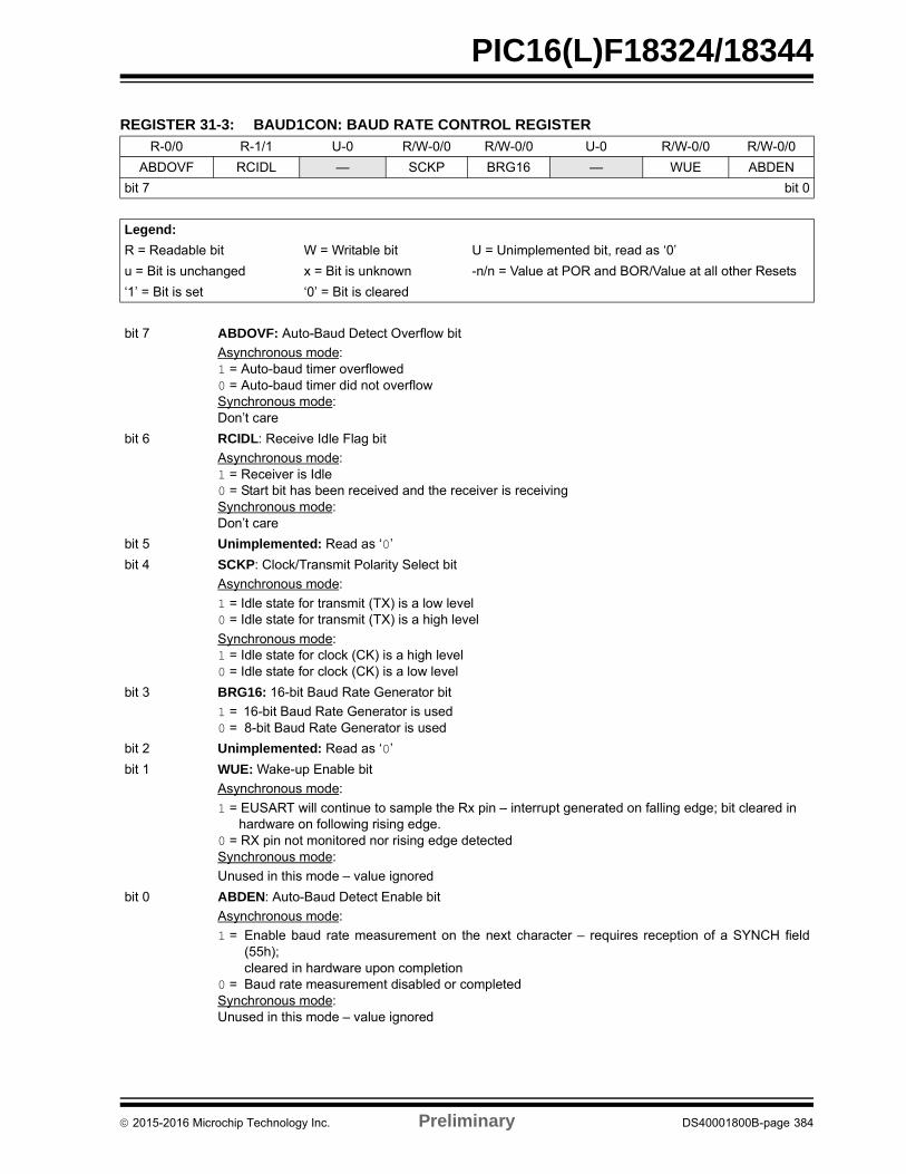
PIC16(L)F18324/18344
REGISTER 31-3: BAUD1CON: BAUD RATE CONTROL REGISTER
R-0/0 R-1/1 U-0 R/W-0/0 R/W-0/0 U-0 R/W-0/0 R/W-0/0
ABDOVF RCIDL — SCKP BRG16 — WUE ABDEN
bit 7 bit 0
Legend:
R = Readable bit W = Writable bit U = Unimplemented bit, read as ‘0’
u = Bit is unchanged x = Bit is unknown -n/n = Value at POR and BOR/Value at all other Resets
‘1’ = Bit is set ‘0’ = Bit is cleared
bit 7 ABDOVF: Auto-Baud Detect Overflow bit
Asynchronous mode:1 = Auto-baud timer overflowed0 = Auto-baud timer did not overflowSynchronous mode:Don’t care
bit 6 RCIDL: Receive Idle Flag bit
Asynchronous mode:1 = Receiver is Idle0 = Start bit has been received and the receiver is receivingSynchronous mode:Don’t care
bit 5 Unimplemented: Read as ‘0’
bit 4 SCKP: Clock/Transmit Polarity Select bit
Asynchronous mode:
1 = Idle state for transmit (TX) is a low level0 = Idle state for transmit (TX) is a high level
Synchronous mode:1 = Idle state for clock (CK) is a high level0 = Idle state for clock (CK) is a low level
bit 3 BRG16: 16-bit Baud Rate Generator bit
1 = 16-bit Baud Rate Generator is used0 = 8-bit Baud Rate Generator is used
bit 2 Unimplemented: Read as ‘0’
bit 1 WUE: Wake-up Enable bit
Asynchronous mode:
1 = EUSART will continue to sample the Rx pin – interrupt generated on falling edge; bit cleared in hardware on following rising edge.
0 = RX pin not monitored nor rising edge detectedSynchronous mode:
Unused in this mode – value ignored
bit 0 ABDEN: Auto-Baud Detect Enable bit
Asynchronous mode:
1 = Enable baud rate measurement on the next character – requires reception of a SYNCH field(55h);cleared in hardware upon completion
0 = Baud rate measurement disabled or completedSynchronous mode:Unused in this mode – value ignored
2015-2016 Microchip Technology Inc. Preliminary DS40001800B-page 384
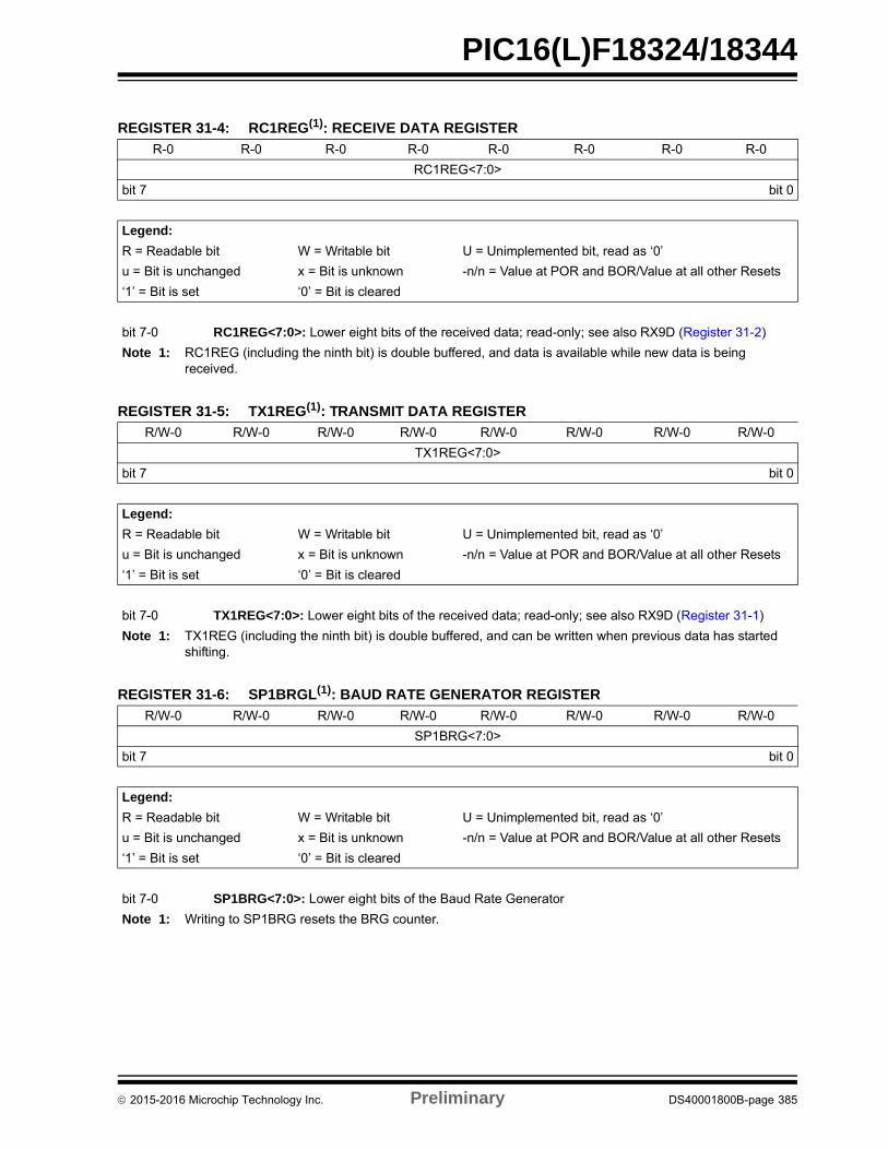
PIC16(L)F18324/18344
REGISTER 31-4: RC1REG(1): RECEIVE DATA REGISTER
R-0 R-0 R-0 R-0 R-0 R-0 R-0 R-0
RC1REG<7:0>
bit 7 bit 0
Legend:
R = Readable bit W = Writable bit U = Unimplemented bit, read as ‘0’
u = Bit is unchanged x = Bit is unknown -n/n = Value at POR and BOR/Value at all other Resets
‘1’ = Bit is set ‘0’ = Bit is cleared
bit 7-0 RC1REG<7:0>: Lower eight bits of the received data; read-only; see also RX9D (Register 31-2)
Note 1: RC1REG (including the ninth bit) is double buffered, and data is available while new data is being received.
REGISTER 31-5: TX1REG(1): TRANSMIT DATA REGISTER
R/W-0 R/W-0 R/W-0 R/W-0 R/W-0 R/W-0 R/W-0 R/W-0
TX1REG<7:0>
bit 7 bit 0
Legend:
R = Readable bit W = Writable bit U = Unimplemented bit, read as ‘0’
u = Bit is unchanged x = Bit is unknown -n/n = Value at POR and BOR/Value at all other Resets
‘1’ = Bit is set ‘0’ = Bit is cleared
bit 7-0 TX1REG<7:0>: Lower eight bits of the received data; read-only; see also RX9D (Register 31-1)
Note 1: TX1REG (including the ninth bit) is double buffered, and can be written when previous data has started shifting.
REGISTER 31-6: SP1BRGL(1): BAUD RATE GENERATOR REGISTER
R/W-0 R/W-0 R/W-0 R/W-0 R/W-0 R/W-0 R/W-0 R/W-0
SP1BRG<7:0>
bit 7 bit 0
Legend:
R = Readable bit W = Writable bit U = Unimplemented bit, read as ‘0’
u = Bit is unchanged x = Bit is unknown -n/n = Value at POR and BOR/Value at all other Resets
‘1’ = Bit is set ‘0’ = Bit is cleared
bit 7-0 SP1BRG<7:0>: Lower eight bits of the Baud Rate Generator
Note 1: Writing to SP1BRG resets the BRG counter.
2015-2016 Microchip Technology Inc. Preliminary DS40001800B-page 385
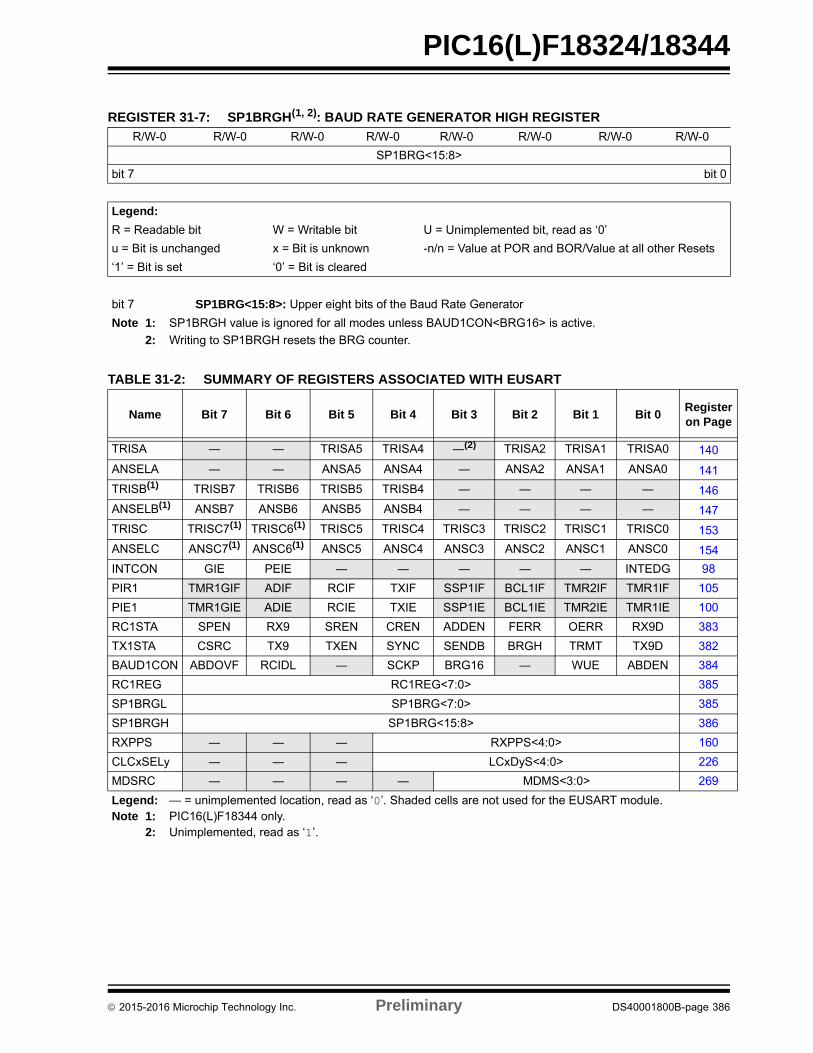
PIC16(L)F18324/18344
REGISTER 31-7: SP1BRGH(1, 2): BAUD RATE GENERATOR HIGH REGISTER
R/W-0 R/W-0 R/W-0 R/W-0 R/W-0 R/W-0 R/W-0 R/W-0
SP1BRG<15:8>
bit 7 bit 0
Legend:
R = Readable bit W = Writable bit U = Unimplemented bit, read as ‘0’
u = Bit is unchanged x = Bit is unknown -n/n = Value at POR and BOR/Value at all other Resets
‘1’ = Bit is set ‘0’ = Bit is cleared
bit 7 SP1BRG<15:8>: Upper eight bits of the Baud Rate Generator
Note 1: SP1BRGH value is ignored for all modes unless BAUD1CON<BRG16> is active.
2: Writing to SP1BRGH resets the BRG counter.
TABLE 31-2: SUMMARY OF REGISTERS ASSOCIATED WITH EUSART
Name Bit 7 Bit 6 Bit 5 Bit 4 Bit 3 Bit 2 Bit 1 Bit 0Register on Page
TRISA ― ― TRISA5 TRISA4 ―(2) TRISA2 TRISA1 TRISA0 140
ANSELA ― ― ANSA5 ANSA4 ― ANSA2 ANSA1 ANSA0 141
TRISB(1) TRISB7 TRISB6 TRISB5 TRISB4 ― ― ― ― 146
ANSELB(1) ANSB7 ANSB6 ANSB5 ANSB4 ― ― ― ― 147
TRISC TRISC7(1) TRISC6(1) TRISC5 TRISC4 TRISC3 TRISC2 TRISC1 TRISC0 153
ANSELC ANSC7(1) ANSC6(1) ANSC5 ANSC4 ANSC3 ANSC2 ANSC1 ANSC0 154
INTCON GIE PEIE ― ― ― ― ― INTEDG 98
PIR1 TMR1GIF ADIF RCIF TXIF SSP1IF BCL1IF TMR2IF TMR1IF 105
PIE1 TMR1GIE ADIE RCIE TXIE SSP1IE BCL1IE TMR2IE TMR1IE 100
RC1STA SPEN RX9 SREN CREN ADDEN FERR OERR RX9D 383
TX1STA CSRC TX9 TXEN SYNC SENDB BRGH TRMT TX9D 382
BAUD1CON ABDOVF RCIDL ― SCKP BRG16 ― WUE ABDEN 384
RC1REG RC1REG<7:0> 385
SP1BRGL SP1BRG<7:0> 385
SP1BRGH SP1BRG<15:8> 386
RXPPS ― ― ― RXPPS<4:0> 160
CLCxSELy ― ― ― LCxDyS<4:0> 226
MDSRC ― ― ― ― MDMS<3:0> 269
Legend: — = unimplemented location, read as ‘0’. Shaded cells are not used for the EUSART module.Note 1: PIC16(L)F18344 only.
2: Unimplemented, read as ‘1’.
2015-2016 Microchip Technology Inc. Preliminary DS40001800B-page 386
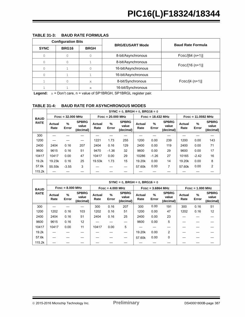
PIC16(L)F18324/18344
TABLE 31-3: BAUD RATE FORMULAS
Configuration BitsBRG/EUSART Mode Baud Rate Formula
SYNC BRG16 BRGH
0 0 0 8-bit/Asynchronous FOSC/[64 (n+1)]
0 0 1 8-bit/AsynchronousFOSC/[16 (n+1)]
0 1 0 16-bit/Asynchronous
0 1 1 16-bit/Asynchronous
FOSC/[4 (n+1)]1 0 x 8-bit/Synchronous
1 1 x 16-bit/Synchronous
Legend: x = Don’t care, n = value of SP1BRGH, SP1BRGL register pair.
TABLE 31-4: BAUD RATE FOR ASYNCHRONOUS MODES
BAUDRATE
SYNC = 0, BRGH = 0, BRG16 = 0
FOSC = 32.000 MHz FOSC = 20.000 MHz FOSC = 18.432 MHz FOSC = 11.0592 MHz
ActualRate
%Error
SPBRGvalue
(decimal)
ActualRate
%Error
SPBRGvalue
(decimal)
ActualRate
%Error
SPBRGvalue
(decimal)
ActualRate
%Error
SPBRGvalue
(decimal)
300 — — — — — — — — — — — —
1200 — — — 1221 1.73 255 1200 0.00 239 1200 0.00 143
2400 2404 0.16 207 2404 0.16 129 2400 0.00 119 2400 0.00 71
9600 9615 0.16 51 9470 -1.36 32 9600 0.00 29 9600 0.00 17
10417 10417 0.00 47 10417 0.00 29 10286 -1.26 27 10165 -2.42 16
19.2k 19.23k 0.16 25 19.53k 1.73 15 19.20k 0.00 14 19.20k 0.00 8
57.6k 55.55k -3.55 3 — — — 57.60k 0.00 7 57.60k 0.00 2
115.2k — — — — — — — — — — — —
BAUDRATE
SYNC = 0, BRGH = 0, BRG16 = 0
FOSC = 8.000 MHz FOSC = 4.000 MHz FOSC = 3.6864 MHz FOSC = 1.000 MHz
ActualRate
%Error
SPBRGvalue
(decimal)
ActualRate
%Error
SPBRGvalue
(decimal)
ActualRate
%Error
SPBRGvalue
(decimal)
ActualRate
%Error
SPBRGvalue
(decimal)
300 — — — 300 0.16 207 300 0.00 191 300 0.16 51
1200 1202 0.16 103 1202 0.16 51 1200 0.00 47 1202 0.16 12
2400 2404 0.16 51 2404 0.16 25 2400 0.00 23 — — —
9600 9615 0.16 12 — — — 9600 0.00 5 — — —
10417 10417 0.00 11 10417 0.00 5 — — — — — —
19.2k — — — — — — 19.20k 0.00 2 — — —
57.6k — — — — — — 57.60k 0.00 0 — — —
115.2k — — — — — — — — — — — —
2015-2016 Microchip Technology Inc. Preliminary DS40001800B-page 387
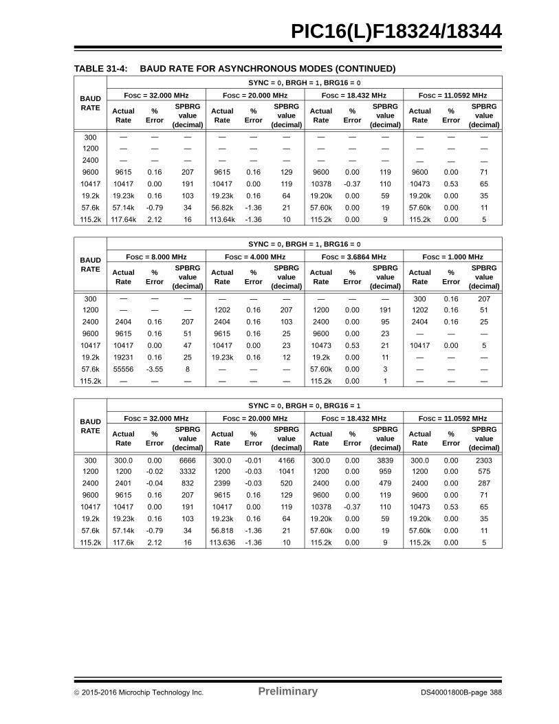
PIC16(L)F18324/18344
BAUDRATE
SYNC = 0, BRGH = 1, BRG16 = 0
FOSC = 32.000 MHz FOSC = 20.000 MHz FOSC = 18.432 MHz FOSC = 11.0592 MHz
ActualRate
%Error
SPBRGvalue
(decimal)
ActualRate
%Error
SPBRGvalue
(decimal)
ActualRate
%Error
SPBRGvalue
(decimal)
ActualRate
%Error
SPBRGvalue
(decimal)
300 — — — — — — — — — — — —
1200 — — — — — — — — — — — —
2400 — — — — — — — — — — — —
9600 9615 0.16 207 9615 0.16 129 9600 0.00 119 9600 0.00 71
10417 10417 0.00 191 10417 0.00 119 10378 -0.37 110 10473 0.53 65
19.2k 19.23k 0.16 103 19.23k 0.16 64 19.20k 0.00 59 19.20k 0.00 35
57.6k 57.14k -0.79 34 56.82k -1.36 21 57.60k 0.00 19 57.60k 0.00 11
115.2k 117.64k 2.12 16 113.64k -1.36 10 115.2k 0.00 9 115.2k 0.00 5
BAUDRATE
SYNC = 0, BRGH = 1, BRG16 = 0
FOSC = 8.000 MHz FOSC = 4.000 MHz FOSC = 3.6864 MHz FOSC = 1.000 MHz
ActualRate
%Error
SPBRGvalue
(decimal)
ActualRate
%Error
SPBRGvalue
(decimal)
ActualRate
%Error
SPBRGvalue
(decimal)
ActualRate
%Error
SPBRGvalue
(decimal)
300 — — — — — — — — — 300 0.16 207
1200 — — — 1202 0.16 207 1200 0.00 191 1202 0.16 51
2400 2404 0.16 207 2404 0.16 103 2400 0.00 95 2404 0.16 25
9600 9615 0.16 51 9615 0.16 25 9600 0.00 23 — — —
10417 10417 0.00 47 10417 0.00 23 10473 0.53 21 10417 0.00 5
19.2k 19231 0.16 25 19.23k 0.16 12 19.2k 0.00 11 — — —
57.6k 55556 -3.55 8 — — — 57.60k 0.00 3 — — —
115.2k — — — — — — 115.2k 0.00 1 — — —
BAUDRATE
SYNC = 0, BRGH = 0, BRG16 = 1
FOSC = 32.000 MHz FOSC = 20.000 MHz FOSC = 18.432 MHz FOSC = 11.0592 MHz
ActualRate
%Error
SPBRGvalue
(decimal)
ActualRate
%Error
SPBRGvalue
(decimal)
ActualRate
%Error
SPBRGvalue
(decimal)
ActualRate
%Error
SPBRGvalue
(decimal)
300 300.0 0.00 6666 300.0 -0.01 4166 300.0 0.00 3839 300.0 0.00 2303
1200 1200 -0.02 3332 1200 -0.03 1041 1200 0.00 959 1200 0.00 575
2400 2401 -0.04 832 2399 -0.03 520 2400 0.00 479 2400 0.00 287
9600 9615 0.16 207 9615 0.16 129 9600 0.00 119 9600 0.00 71
10417 10417 0.00 191 10417 0.00 119 10378 -0.37 110 10473 0.53 65
19.2k 19.23k 0.16 103 19.23k 0.16 64 19.20k 0.00 59 19.20k 0.00 35
57.6k 57.14k -0.79 34 56.818 -1.36 21 57.60k 0.00 19 57.60k 0.00 11
115.2k 117.6k 2.12 16 113.636 -1.36 10 115.2k 0.00 9 115.2k 0.00 5
TABLE 31-4: BAUD RATE FOR ASYNCHRONOUS MODES (CONTINUED)
2015-2016 Microchip Technology Inc. Preliminary DS40001800B-page 388
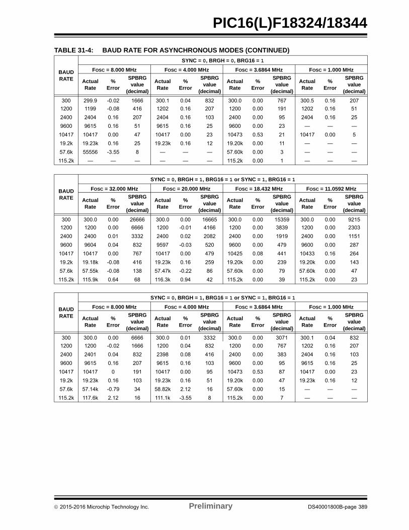
PIC16(L)F18324/18344
BAUDRATE
SYNC = 0, BRGH = 0, BRG16 = 1
FOSC = 8.000 MHz FOSC = 4.000 MHz FOSC = 3.6864 MHz FOSC = 1.000 MHz
ActualRate
%Error
SPBRGvalue
(decimal)
ActualRate
%Error
SPBRGvalue
(decimal)
ActualRate
%Error
SPBRGvalue
(decimal)
ActualRate
%Error
SPBRGvalue
(decimal)
300 299.9 -0.02 1666 300.1 0.04 832 300.0 0.00 767 300.5 0.16 207
1200 1199 -0.08 416 1202 0.16 207 1200 0.00 191 1202 0.16 51
2400 2404 0.16 207 2404 0.16 103 2400 0.00 95 2404 0.16 25
9600 9615 0.16 51 9615 0.16 25 9600 0.00 23 — — —
10417 10417 0.00 47 10417 0.00 23 10473 0.53 21 10417 0.00 5
19.2k 19.23k 0.16 25 19.23k 0.16 12 19.20k 0.00 11 — — —
57.6k 55556 -3.55 8 — — — 57.60k 0.00 3 — — —
115.2k — — — — — — 115.2k 0.00 1 — — —
BAUDRATE
SYNC = 0, BRGH = 1, BRG16 = 1 or SYNC = 1, BRG16 = 1
FOSC = 32.000 MHz FOSC = 20.000 MHz FOSC = 18.432 MHz FOSC = 11.0592 MHz
ActualRate
%Error
SPBRGvalue
(decimal)
ActualRate
%Error
SPBRGvalue
(decimal)
ActualRate
%Error
SPBRGvalue
(decimal)
ActualRate
%Error
SPBRGvalue
(decimal)
300 300.0 0.00 26666 300.0 0.00 16665 300.0 0.00 15359 300.0 0.00 9215
1200 1200 0.00 6666 1200 -0.01 4166 1200 0.00 3839 1200 0.00 2303
2400 2400 0.01 3332 2400 0.02 2082 2400 0.00 1919 2400 0.00 1151
9600 9604 0.04 832 9597 -0.03 520 9600 0.00 479 9600 0.00 287
10417 10417 0.00 767 10417 0.00 479 10425 0.08 441 10433 0.16 264
19.2k 19.18k -0.08 416 19.23k 0.16 259 19.20k 0.00 239 19.20k 0.00 143
57.6k 57.55k -0.08 138 57.47k -0.22 86 57.60k 0.00 79 57.60k 0.00 47
115.2k 115.9k 0.64 68 116.3k 0.94 42 115.2k 0.00 39 115.2k 0.00 23
BAUDRATE
SYNC = 0, BRGH = 1, BRG16 = 1 or SYNC = 1, BRG16 = 1
FOSC = 8.000 MHz FOSC = 4.000 MHz FOSC = 3.6864 MHz FOSC = 1.000 MHz
ActualRate
%Error
SPBRGvalue
(decimal)
ActualRate
%Error
SPBRGvalue
(decimal)
ActualRate
%Error
SPBRGvalue
(decimal)
ActualRate
%Error
SPBRGvalue
(decimal)
300 300.0 0.00 6666 300.0 0.01 3332 300.0 0.00 3071 300.1 0.04 832
1200 1200 -0.02 1666 1200 0.04 832 1200 0.00 767 1202 0.16 207
2400 2401 0.04 832 2398 0.08 416 2400 0.00 383 2404 0.16 103
9600 9615 0.16 207 9615 0.16 103 9600 0.00 95 9615 0.16 25
10417 10417 0 191 10417 0.00 95 10473 0.53 87 10417 0.00 23
19.2k 19.23k 0.16 103 19.23k 0.16 51 19.20k 0.00 47 19.23k 0.16 12
57.6k 57.14k -0.79 34 58.82k 2.12 16 57.60k 0.00 15 — — —
115.2k 117.6k 2.12 16 111.1k -3.55 8 115.2k 0.00 7 — — —
TABLE 31-4: BAUD RATE FOR ASYNCHRONOUS MODES (CONTINUED)
2015-2016 Microchip Technology Inc. Preliminary DS40001800B-page 389
PIC16(L)F18324/18344
32.0 REFERENCE CLOCK OUTPUT MODULE
The Reference Clock Output module provides theability to send a clock signal to the clock referenceoutput pin (CLKR). The Reference Clock Output canalso be used as a signal for other peripherals, such asthe Data Signal Modulator (DSM).
The Reference Clock Output module has the followingfeatures:
• System clock is the module source clock• Programmable clock divider• Selectable duty cycle
32.1 Clock Source
The Reference Clock Output module uses the systemclock (FOSC) as the clock source. Any device clockswitching will be reflected in the clock output.
32.1.1 CLOCK SYNCHRONIZATION
Once the reference clock enable (CLKREN) is set, themodule is ensured to be glitch-free at start-up.
When the Reference Clock Output is disabled, theoutput signal will be disabled immediately.
Clock dividers and clock duty cycles can be changedwhile the module is enabled, but glitches may occur onthe output. To avoid possible glitches, clock dividersand clock duty cycles should be changed only when theCLKREN is clear.
32.2 Programmable Clock Divider
The module takes the system clock input and divides itbased on the value of the CLKRDIV<2:0> bits of theCLKRCON register (Register 32-1).
The following configurations can be made based on theCLKRDIV<2:0> bits:
• Base FOSC value• FOSC divided by 2• FOSC divided by 4• FOSC divided by 8• FOSC divided by 16• FOSC divided by 32• FOSC divided by 64• FOSC divided by 128
The clock divider values can be changed while themodule is enabled; however, in order to preventglitches on the output, the CLKRDIV<2:0> bits shouldonly be changed when the module is disabled(CLKREN = 0).
32.3 Selectable Duty Cycle
The CLKRDC<1:0> bits of the CLKRCON register canbe used to modify the duty cycle of the output clock. Aduty cycle of 25%, 50%, or 75% can be selected for allclock rates, with the exception of the undivided baseFOSC value.
The duty cycle can be changed while the module isenabled; however, in order to prevent glitches on theoutput, the CLKRDC<1:0> bits should only be changedwhen the module is disabled (CLKREN = 0).
32.4 Operation in Sleep Mode
The Reference Clock Output module clock is based onthe system clock. When the device goes to Sleep, themodule outputs will remain in their current state. Thiswill have a direct effect on peripherals using theReference Clock Output as an input signal.
Note: The CLKRDC1 bit is reset to ‘1’. Thismakes the default duty cycle 50%.
2015-2016 Microchip Technology Inc. Preliminary DS40001800B-page 390
PIC16(L)F18324/18344
FIGURE 32-1: CLOCK REFERENCE BLOCK DIAGRAM
FIGURE 32-2: CLOCK REFERENCE TIMING
D
EN
QFOSC
CLKREN
FREEZE ENABLED(1)
ICD FREEZE MODE(1)
CLKRDIV<2:0>
Duty Cycle
CLKRDC<1:0>
CLKR
To Peripherals
Note 1: Freeze is used in Debug Mode only; otherwise read as ‘0’
000
011010001
100101110111
FOSC/2
FOSC/4
FOSC/8
FOSC/16
FOSC/32
FOSC/64
FOSC/128
CLKREN Counter Reset
Clock Counter
FOSC
CLKREN
CLKRDIV[2:0] = 001CLKRDC[1:0] = 10
CLKRDC[1:0] = 01CLKRDIV[2:0] = 001
CLKR Output
Duty Cycle (25%)
Duty Cycle (50%)
FOSC / 2
P1 P2
CLKR Output
2015-2016 Microchip Technology Inc. Preliminary DS40001800B-page 391
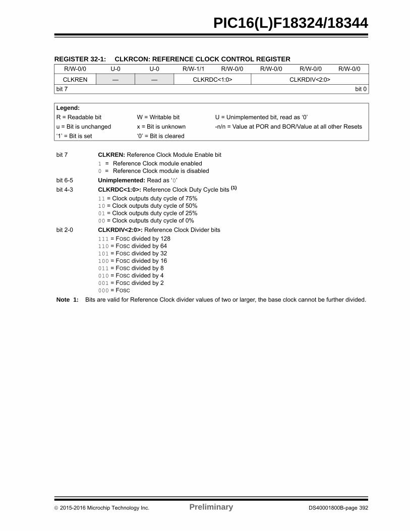
PIC16(L)F18324/18344
REGISTER 32-1: CLKRCON: REFERENCE CLOCK CONTROL REGISTER
R/W-0/0 U-0 U-0 R/W-1/1 R/W-0/0 R/W-0/0 R/W-0/0 R/W-0/0
CLKREN — — CLKRDC<1:0> CLKRDIV<2:0>
bit 7 bit 0
Legend:
R = Readable bit W = Writable bit U = Unimplemented bit, read as ‘0’
u = Bit is unchanged x = Bit is unknown -n/n = Value at POR and BOR/Value at all other Resets
‘1’ = Bit is set ‘0’ = Bit is cleared
bit 7 CLKREN: Reference Clock Module Enable bit
1 = Reference Clock module enabled0 = Reference Clock module is disabled
bit 6-5 Unimplemented: Read as ‘0’
bit 4-3 CLKRDC<1:0>: Reference Clock Duty Cycle bits (1)
11 = Clock outputs duty cycle of 75%10 = Clock outputs duty cycle of 50%01 = Clock outputs duty cycle of 25%00 = Clock outputs duty cycle of 0%
bit 2-0 CLKRDIV<2:0>: Reference Clock Divider bits
111 = FOSC divided by 128110 = FOSC divided by 64101 = FOSC divided by 32100 = FOSC divided by 16011 = FOSC divided by 8010 = FOSC divided by 4001 = FOSC divided by 2000 = FOSC
Note 1: Bits are valid for Reference Clock divider values of two or larger, the base clock cannot be further divided.
2015-2016 Microchip Technology Inc. Preliminary DS40001800B-page 392
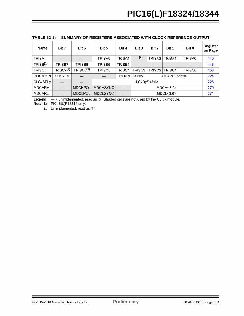
PIC16(L)F18324/18344
TABLE 32-1: SUMMARY OF REGISTERS ASSOCIATED WITH CLOCK REFERENCE OUTPUT
Name Bit 7 Bit 6 Bit 5 Bit 4 Bit 3 Bit 2 Bit 1 Bit 0Register on Page
TRISA ― ― TRISA5 TRISA4 ―(2) TRISA2 TRISA1 TRISA0 140
TRISB(1) TRISB7 TRISB6 TRISB5 TRISB4 ― ― ― ― 146
TRISC TRISC7(1) TRISC6(1) TRISC5 TRISC4 TRISC3 TRISC2 TRISC1 TRISC0 153
CLKRCON CLKREN ― ― CLKRDC<1:0> CLKRDIV<2:0> 224
CLCxSELy ― ― LCxDyS<5:0> 226
MDCARH ― MDCHPOL MDCHSYNC ― MDCH<3:0> 270
MDCARL ― MDCLPOL MDCLSYNC ― MDCL<3:0> 271
Legend: — = unimplemented, read as ‘0’. Shaded cells are not used by the CLKR module.Note 1: PIC16(L)F18344 only.
2: Unimplemented, read as ‘1’.
2015-2016 Microchip Technology Inc. Preliminary DS40001800B-page 393
PIC16(L)F18324/18344
33.0 IN-CIRCUIT SERIAL PROGRAMMING™ (ICSP™)
ICSP™ programming allows customers to manufacturecircuit boards with unprogrammed devices. Programmingcan be done after the assembly process, allowing thedevice to be programmed with the most recent firmwareor a custom firmware. Five pins are needed for ICSP™programming:• ICSPCLK• ICSPDAT• MCLR/VPP
• VDD
• VSS
In Program/Verify mode the program memory, dataEEPROM, User IDs and the Configuration Words areprogrammed through serial communications. TheICSPDAT pin is a bidirectional I/O used for transferringthe serial data and the ICSPCLK pin is the clock input.For more information on ICSP™ refer to the“PIC16(L)F183XX Memory ProgrammingSpecification” (DS40001738).
33.1 High-Voltage Programming Entry Mode
The device is placed into High-Voltage ProgrammingEntry mode by holding the ICSPCLK and ICSPDATpins low then raising the voltage on MCLR/VPP to VIHH.
33.2 Low-Voltage Programming Entry Mode
The Low-Voltage Programming Entry mode allows thePIC® Flash MCUs to be programmed using VDD only,without high voltage. When the LVP bit of ConfigurationWords is set to ‘1’, the low-voltage ICSP programmingentry is enabled. To disable the Low-Voltage ICSPmode, the LVP bit must be programmed to ‘0’. The LVPbit can only be reprogrammed to ‘0’ by using theHigh-Voltage Programming mode.
Entry into the Low-Voltage Programming Entry moderequires the following steps:
1. MCLR is brought to VIL.
2. A 32-bit key sequence is presented onICSPDAT, while clocking ICSPCLK.
Once the key sequence is complete, MCLR must beheld at VIL for as long as Program/Verify mode is to bemaintained.
If low-voltage programming is enabled (LVP = 1), theMCLR Reset function is automatically enabled andcannot be disabled. See Section 6.4 “MCLR” for moreinformation.
33.3 Common Programming Interfaces
Connection to a target device is typically done throughan ICSP™ header. A commonly found connector ondevelopment tools is the RJ-11 in the 6P6C (6-pin,6-connector) configuration. See Figure 33-1.
FIGURE 33-1: ICD RJ-11 STYLE CONNECTOR INTERFACE
Another connector often found in use with the PICkit™programmers is a standard 6-pin header with 0.1 inchspacing. Refer to Figure 33-2.
For additional interface recommendations, refer to yourspecific device programmer manual prior to PCBdesign.
It is recommended that isolation devices be used toseparate the programming pins from other circuitry.The type of isolation is highly dependent on the specificapplication and may include devices such as resistors,diodes, or even jumpers. See Figure 33-3 for moreinformation.
1
2
3
4
5
6
Target
Bottom SidePC BoardVPP/MCLR VSS
ICSPCLKVDD
ICSPDATNC
Pin Description*
1 = VPP/MCLR
2 = VDD Target
3 = VSS (ground)
4 = ICSPDAT
5 = ICSPCLK
6 = No Connect
2015-2016 Microchip Technology Inc. Preliminary DS40001800B-page 394
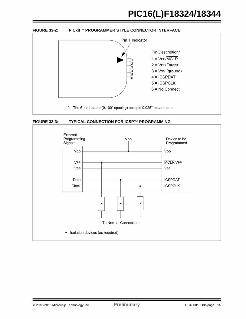
PIC16(L)F18324/18344
FIGURE 33-2: PICkit™ PROGRAMMER STYLE CONNECTOR INTERFACE
FIGURE 33-3: TYPICAL CONNECTION FOR ICSP™ PROGRAMMING
123456
* The 6-pin header (0.100" spacing) accepts 0.025" square pins.
Pin Description*
1 = VPP/MCLR
2 = VDD Target
3 = VSS (ground)
4 = ICSPDAT
5 = ICSPCLK
6 = No Connect
Pin 1 Indicator
VDD
VPP
VSS
ExternalDevice to be
Data
Clock
VDD
MCLR/VPP
VSS
ICSPDAT
ICSPCLK
* **
To Normal Connections
* Isolation devices (as required).
Programming Signals Programmed
VDD
2015-2016 Microchip Technology Inc. Preliminary DS40001800B-page 395
PIC16(L)F18324/18344
34.0 INSTRUCTION SET SUMMARY
Each instruction is a 14-bit word containing the opera-tion code (opcode) and all required operands. Theopcodes are broken into three broad categories.
• Byte Oriented• Bit Oriented• Literal and Control
The literal and control category contains the mostvaried instruction word format.
Table 34-3 lists the instructions recognized by theMPASM™ assembler.
All instructions are executed within a single instructioncycle, with the following exceptions, which may taketwo or three cycles:
• Subroutine entry takes two cycles (CALL, CALLW)• Returns from interrupts or subroutines take two
cycles (RETURN, RETLW, RETFIE)• Program branching takes two cycles (GOTO, BRA, BRW, BTFSS, BTFSC, DECFSZ, INCSFZ)
• One additional instruction cycle will be used when any instruction references an indirect file register and the file select register is pointing to program memory.
One instruction cycle consists of 4 oscillator cycles; foran oscillator frequency of 4 MHz, this gives a nominalinstruction execution rate of 1 MHz.
All instruction examples use the format ‘0xhh’ torepresent a hexadecimal number, where ‘h’ signifies ahexadecimal digit.
34.1 Read-Modify-Write Operations
Any write instruction that specifies a file register as partof the instruction performs a Read-Modify-Write(R-M-W) operation. The register is read, the data ismodified, and the result is stored according to either theworking (W) register, or the originating file register,depending on the state of the destination designator ‘d’(see Table 34-1 for more information). A read operationis performed on a register even if the instruction writesto that register.
TABLE 34-1: OPCODE FIELD DESCRIPTIONS
Field Description
f Register file address (0x00 to 0x7F)
W Working register (accumulator)
b Bit address within an 8-bit file register
k Literal field, constant data or label
x Don’t care location (= 0 or 1). The assembler will generate code with x = 0. It is the recommended form of use for compatibility with all Microchip software tools.
d Destination select; d = 0: store result in W,d = 1: store result in file register f.
n FSR or INDF number. (0-1)
mm Pre-post increment-decrement mode selection
TABLE 34-2: ABBREVIATION DESCRIPTIONS
Field Description
PC Program Counter
TO Time-Out bit
C Carry bit
DC Digit Carry bit
Z Zero bit
PD Power-Down bit
2015-2016 Microchip Technology Inc. Preliminary DS40001800B-page 396
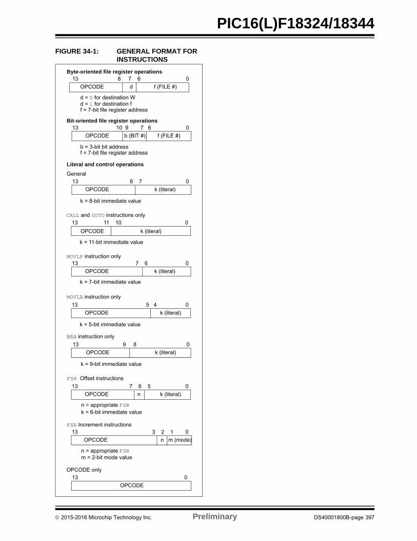
PIC16(L)F18324/18344
FIGURE 34-1: GENERAL FORMAT FOR INSTRUCTIONS
Byte-oriented file register operations13 8 7 6 0
d = 0 for destination W
OPCODE d f (FILE #)
d = 1 for destination ff = 7-bit file register address
Bit-oriented file register operations13 10 9 7 6 0
OPCODE b (BIT #) f (FILE #)
b = 3-bit bit addressf = 7-bit file register address
Literal and control operations
13 8 7 0
OPCODE k (literal)
k = 8-bit immediate value
13 11 10 0
OPCODE k (literal)
k = 11-bit immediate value
General
CALL and GOTO instructions only
MOVLP instruction only
13 5 4 0
OPCODE k (literal)
k = 5-bit immediate value
MOVLB instruction only
13 9 8 0
OPCODE k (literal)
k = 9-bit immediate value
BRA instruction only
FSR Offset instructions
13 7 6 5 0
OPCODE n k (literal)
n = appropriate FSR
FSR Increment instructions
13 7 6 0
OPCODE k (literal)
k = 7-bit immediate value
13 3 2 1 0
OPCODE n m (mode)
n = appropriate FSRm = 2-bit mode value
k = 6-bit immediate value
13 0
OPCODE
OPCODE only
2015-2016 Microchip Technology Inc. Preliminary DS40001800B-page 397
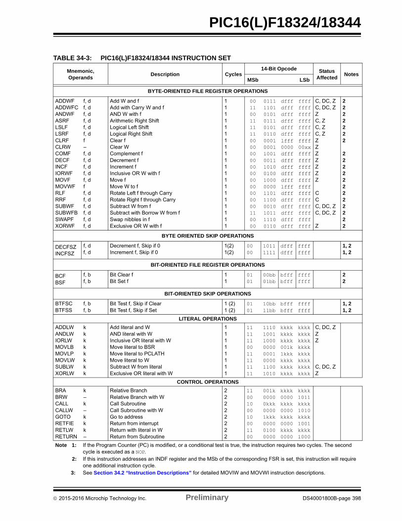
PIC16(L)F18324/18344
TABLE 34-3: PIC16(L)F18324/18344 INSTRUCTION SET
Mnemonic,Operands
Description Cycles14-Bit Opcode Status
AffectedNotes
MSb LSb
BYTE-ORIENTED FILE REGISTER OPERATIONS
ADDWFADDWFCANDWFASRFLSLFLSRFCLRFCLRWCOMFDECFINCFIORWFMOVFMOVWFRLFRRFSUBWFSUBWFBSWAPFXORWF
f, df, df, df, df, df, df–f, df, df, df, df, dff, df, df, df, df, df, d
Add W and fAdd with Carry W and fAND W with fArithmetic Right ShiftLogical Left ShiftLogical Right ShiftClear fClear WComplement fDecrement fIncrement fInclusive OR W with fMove fMove W to fRotate Left f through CarryRotate Right f through CarrySubtract W from fSubtract with Borrow W from fSwap nibbles in fExclusive OR W with f
11111111111111111111
0011001111110000000000000000000000110000
01111101010101110101011000010001100100111010010010000000110111000010101111100110
dfffdfffdfffdfffdfffdffflfff0000dfffdfffdfffdfffdfff1fffdfffdfffdfffdfffdfffdfff
ffffffffffffffffffffffffffff00xxffffffffffffffffffffffffffffffffffffffffffffffff
C, DC, ZC, DC, ZZC, ZC, ZC, ZZZZZZZZ
CCC, DC, ZC, DC, Z
Z
2222222
222222222222
BYTE ORIENTED SKIP OPERATIONS
DECFSZINCFSZ
f, df, d
Decrement f, Skip if 0Increment f, Skip if 0
1(2)1(2)
0000
10111111
dfffdfff
ffffffff
1, 21, 2
BIT-ORIENTED FILE REGISTER OPERATIONS
BCFBSF
f, bf, b
Bit Clear fBit Set f
11
0101
00bb01bb
bfffbfff
ffffffff
22
BIT-ORIENTED SKIP OPERATIONS
BTFSCBTFSS
f, bf, b
Bit Test f, Skip if ClearBit Test f, Skip if Set
1 (2)1 (2)
0101
10bb11bb
bfff bfff
ffffffff
1, 21, 2
LITERAL OPERATIONS
ADDLWANDLWIORLWMOVLBMOVLPMOVLWSUBLWXORLW
kkkkkkkk
Add literal and WAND literal with WInclusive OR literal with WMove literal to BSRMove literal to PCLATHMove literal to WSubtract W from literalExclusive OR literal with W
11111111
1111110011111111
11101001100000000001000011001010
kkkkkkkkkkkk001k1kkkkkkkkkkkkkkk
kkkkkkkkkkkkkkkkkkkkkkkkkkkkkkkk
C, DC, ZZZ
C, DC, ZZ
CONTROL OPERATIONS
BRABRWCALLCALLWGOTORETFIERETLWRETURN
k–k–kkk–
Relative BranchRelative Branch with WCall SubroutineCall Subroutine with WGo to addressReturn from interruptReturn with literal in WReturn from Subroutine
22222222
1100100010001100
001k00000kkk00001kkk000001000000
kkkk0000kkkk0000kkkk0000kkkk0000
kkkk1011kkkk1010kkkk1001kkkk1000
Note 1: If the Program Counter (PC) is modified, or a conditional test is true, the instruction requires two cycles. The second cycle is executed as a NOP.
2: If this instruction addresses an INDF register and the MSb of the corresponding FSR is set, this instruction will require one additional instruction cycle.
3: See Section 34.2 “Instruction Descriptions” for detailed MOVIW and MOVWI instruction descriptions.
2015-2016 Microchip Technology Inc. Preliminary DS40001800B-page 398
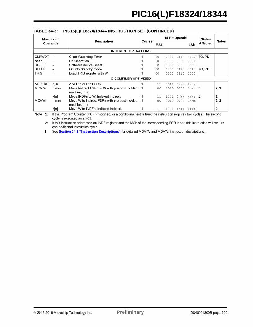
PIC16(L)F18324/18344
INHERENT OPERATIONS
CLRWDTNOPRESETSLEEPTRIS
––––f
Clear Watchdog TimerNo OperationSoftware device ResetGo into Standby modeLoad TRIS register with W
11111
0000000000
00000000000000000000
01100000000001100110
01000000000100110fff
TO, PD
TO, PD
C-COMPILER OPTIMIZED
ADDFSRMOVIW
MOVWI
n, kn mm
k[n]n mm
k[n]
Add Literal k to FSRnMove Indirect FSRn to W with pre/post inc/dec modifier, mmMove INDFn to W, Indexed Indirect.Move W to Indirect FSRn with pre/post inc/dec modifier, mmMove W to INDFn, Indexed Indirect.
11
11
1
1100
1100
11
00010000
11110000
1111
0nkk0001
0nkk0001
1nkk
kkkk0nmm
kkkk1nmm
kkkk
Z
Z
2, 3
22, 3
2
TABLE 34-3: PIC16(L)F18324/18344 INSTRUCTION SET (CONTINUED)
Mnemonic,Operands
Description Cycles14-Bit Opcode Status
AffectedNotes
MSb LSb
Note 1: If the Program Counter (PC) is modified, or a conditional test is true, the instruction requires two cycles. The second cycle is executed as a NOP.
2: If this instruction addresses an INDF register and the MSb of the corresponding FSR is set, this instruction will require one additional instruction cycle.
3: See Section 34.2 “Instruction Descriptions” for detailed MOVIW and MOVWI instruction descriptions.
2015-2016 Microchip Technology Inc. Preliminary DS40001800B-page 399
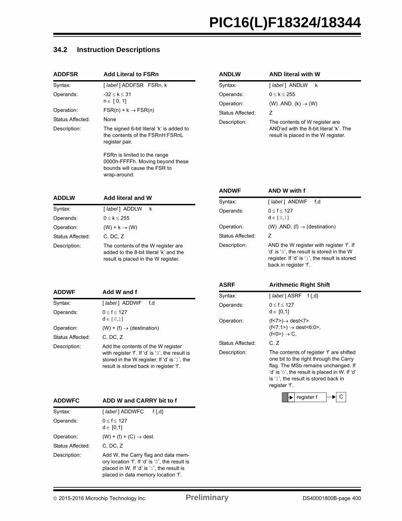
PIC16(L)F18324/18344
34.2 Instruction Descriptions
ADDFSR Add Literal to FSRn
Syntax: [ label ] ADDFSR FSRn, k
Operands: -32 k 31n [ 0, 1]
Operation: FSR(n) + k FSR(n)
Status Affected: None
Description: The signed 6-bit literal ‘k’ is added to the contents of the FSRnH:FSRnL register pair.
FSRn is limited to the range 0000h-FFFFh. Moving beyond these bounds will cause the FSR to wrap-around.
ADDLW Add literal and W
Syntax: [ label ] ADDLW k
Operands: 0 k 255
Operation: (W) + k (W)
Status Affected: C, DC, Z
Description: The contents of the W register are added to the 8-bit literal ‘k’ and the result is placed in the W register.
ADDWF Add W and f
Syntax: [ label ] ADDWF f,d
Operands: 0 f 127d 0,1
Operation: (W) + (f) (destination)
Status Affected: C, DC, Z
Description: Add the contents of the W register with register ‘f’. If ‘d’ is ‘0’, the result is stored in the W register. If ‘d’ is ‘1’, the result is stored back in register ‘f’.
ADDWFC ADD W and CARRY bit to f
Syntax: [ label ] ADDWFC f ,d
Operands: 0 f 127d [0,1]
Operation: (W) + (f) + (C) dest
Status Affected: C, DC, Z
Description: Add W, the Carry flag and data mem-ory location ‘f’. If ‘d’ is ‘0’, the result is placed in W. If ‘d’ is ‘1’, the result is placed in data memory location ‘f’.
ANDLW AND literal with W
Syntax: [ label ] ANDLW k
Operands: 0 k 255
Operation: (W) .AND. (k) (W)
Status Affected: Z
Description: The contents of W register are AND’ed with the 8-bit literal ‘k’. The result is placed in the W register.
ANDWF AND W with f
Syntax: [ label ] ANDWF f,d
Operands: 0 f 127d 0,1
Operation: (W) .AND. (f) (destination)
Status Affected: Z
Description: AND the W register with register ‘f’. If ‘d’ is ‘0’, the result is stored in the W register. If ‘d’ is ‘1’, the result is stored back in register ‘f’.
ASRF Arithmetic Right Shift
Syntax: [ label ] ASRF f ,d
Operands: 0 f 127d [0,1]
Operation: (f<7>) dest<7>(f<7:1>) dest<6:0>,(f<0>) C,
Status Affected: C, Z
Description: The contents of register ‘f’ are shifted one bit to the right through the Carry flag. The MSb remains unchanged. If ‘d’ is ‘0’, the result is placed in W. If ‘d’ is ‘1’, the result is stored back in register ‘f’.
register f C
2015-2016 Microchip Technology Inc. Preliminary DS40001800B-page 400
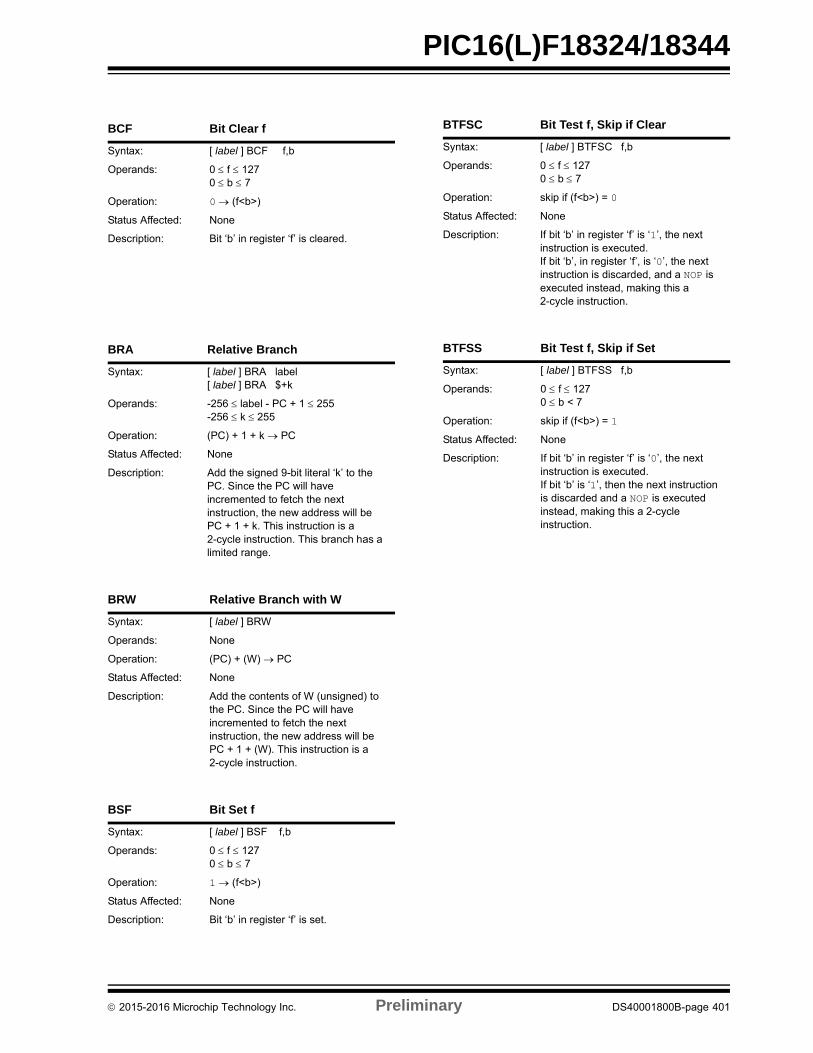
PIC16(L)F18324/18344
BCF Bit Clear f
Syntax: [ label ] BCF f,b
Operands: 0 f 1270 b 7
Operation: 0 (f<b>)
Status Affected: None
Description: Bit ‘b’ in register ‘f’ is cleared.
BRA Relative Branch
Syntax: [ label ] BRA label [ label ] BRA $+k
Operands: -256 label - PC + 1 255-256 k 255
Operation: (PC) + 1 + k PC
Status Affected: None
Description: Add the signed 9-bit literal ‘k’ to the PC. Since the PC will have incremented to fetch the next instruction, the new address will be PC + 1 + k. This instruction is a 2-cycle instruction. This branch has a limited range.
BRW Relative Branch with W
Syntax: [ label ] BRW
Operands: None
Operation: (PC) + (W) PC
Status Affected: None
Description: Add the contents of W (unsigned) to the PC. Since the PC will have incremented to fetch the next instruction, the new address will be PC + 1 + (W). This instruction is a 2-cycle instruction.
BSF Bit Set f
Syntax: [ label ] BSF f,b
Operands: 0 f 1270 b 7
Operation: 1 (f<b>)
Status Affected: None
Description: Bit ‘b’ in register ‘f’ is set.
BTFSC Bit Test f, Skip if Clear
Syntax: [ label ] BTFSC f,b
Operands: 0 f 1270 b 7
Operation: skip if (f<b>) = 0
Status Affected: None
Description: If bit ‘b’ in register ‘f’ is ‘1’, the next instruction is executed.If bit ‘b’, in register ‘f’, is ‘0’, the next instruction is discarded, and a NOP is executed instead, making this a 2-cycle instruction.
BTFSS Bit Test f, Skip if Set
Syntax: [ label ] BTFSS f,b
Operands: 0 f 1270 b < 7
Operation: skip if (f<b>) = 1
Status Affected: None
Description: If bit ‘b’ in register ‘f’ is ‘0’, the next instruction is executed.If bit ‘b’ is ‘1’, then the next instruction is discarded and a NOP is executed instead, making this a 2-cycle instruction.
2015-2016 Microchip Technology Inc. Preliminary DS40001800B-page 401
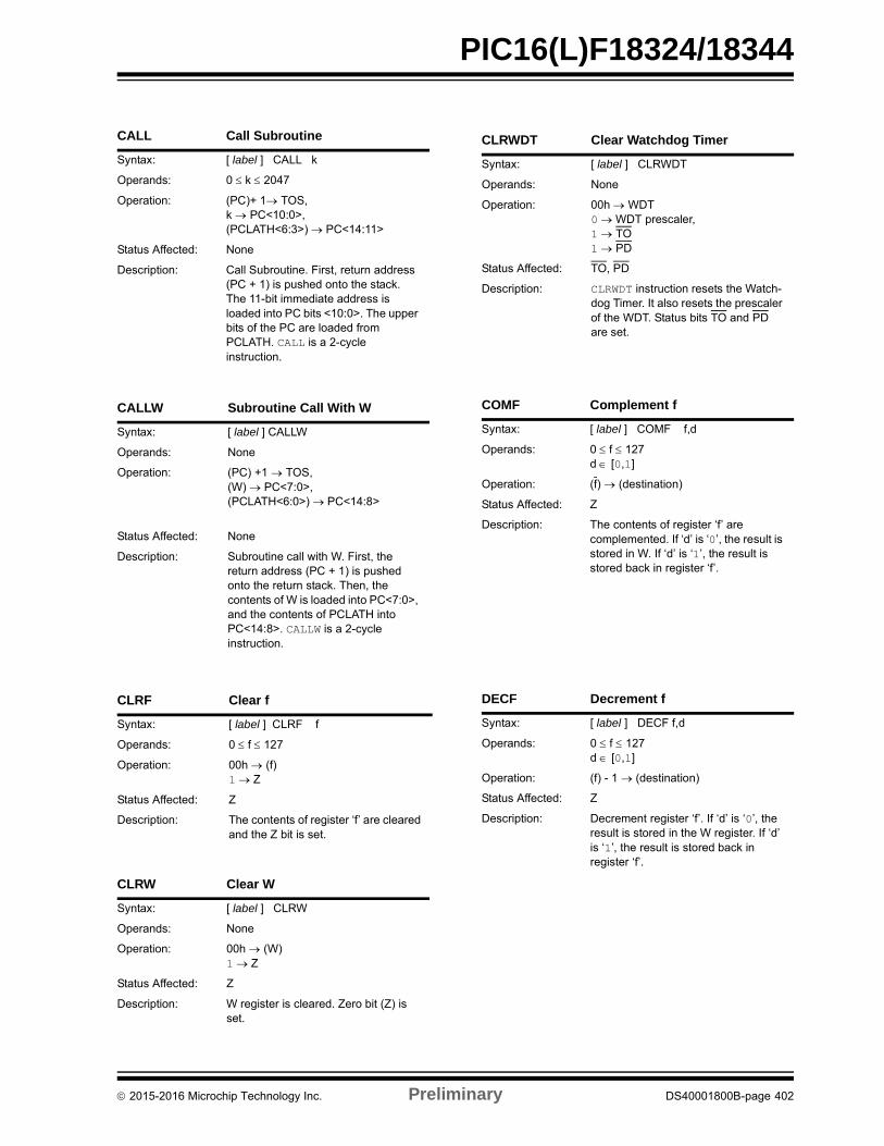
PIC16(L)F18324/18344
CALL Call Subroutine
Syntax: [ label ] CALL k
Operands: 0 k 2047
Operation: (PC)+ 1 TOS,k PC<10:0>,(PCLATH<6:3>) PC<14:11>
Status Affected: None
Description: Call Subroutine. First, return address (PC + 1) is pushed onto the stack. The 11-bit immediate address is loaded into PC bits <10:0>. The upper bits of the PC are loaded from PCLATH. CALL is a 2-cycle instruction.
CALLW Subroutine Call With W
Syntax: [ label ] CALLW
Operands: None
Operation: (PC) +1 TOS,(W) PC<7:0>,(PCLATH<6:0>) PC<14:8>
Status Affected: None
Description: Subroutine call with W. First, the return address (PC + 1) is pushed onto the return stack. Then, the contents of W is loaded into PC<7:0>, and the contents of PCLATH into PC<14:8>. CALLW is a 2-cycle instruction.
CLRF Clear f
Syntax: [ label ] CLRF f
Operands: 0 f 127
Operation: 00h (f)1 Z
Status Affected: Z
Description: The contents of register ‘f’ are cleared and the Z bit is set.
CLRW Clear W
Syntax: [ label ] CLRW
Operands: None
Operation: 00h (W)1 Z
Status Affected: Z
Description: W register is cleared. Zero bit (Z) is set.
CLRWDT Clear Watchdog Timer
Syntax: [ label ] CLRWDT
Operands: None
Operation: 00h WDT0 WDT prescaler,1 TO1 PD
Status Affected: TO, PD
Description: CLRWDT instruction resets the Watch-dog Timer. It also resets the prescaler of the WDT. Status bits TO and PD are set.
COMF Complement f
Syntax: [ label ] COMF f,d
Operands: 0 f 127d [0,1]
Operation: (f) (destination)
Status Affected: Z
Description: The contents of register ‘f’ are complemented. If ‘d’ is ‘0’, the result is stored in W. If ‘d’ is ‘1’, the result is stored back in register ‘f’.
DECF Decrement f
Syntax: [ label ] DECF f,d
Operands: 0 f 127d [0,1]
Operation: (f) - 1 (destination)
Status Affected: Z
Description: Decrement register ‘f’. If ‘d’ is ‘0’, the result is stored in the W register. If ‘d’ is ‘1’, the result is stored back in register ‘f’.
2015-2016 Microchip Technology Inc. Preliminary DS40001800B-page 402
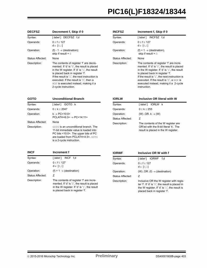
PIC16(L)F18324/18344
DECFSZ Decrement f, Skip if 0
Syntax: [ label ] DECFSZ f,d
Operands: 0 f 127d [0,1]
Operation: (f) - 1 (destination); skip if result = 0
Status Affected: None
Description: The contents of register ‘f’ are decre-mented. If ‘d’ is ‘0’, the result is placed in the W register. If ‘d’ is ‘1’, the result is placed back in register ‘f’. If the result is ‘1’, the next instruction is executed. If the result is ‘0’, then a NOP is executed instead, making it a 2-cycle instruction.
GOTO Unconditional Branch
Syntax: [ label ] GOTO k
Operands: 0 k 2047
Operation: k PC<10:0>PCLATH<6:3> PC<14:11>
Status Affected: None
Description: GOTO is an unconditional branch. The 11-bit immediate value is loaded into PC bits <10:0>. The upper bits of PC are loaded from PCLATH<4:3>. GOTO is a 2-cycle instruction.
INCF Increment f
Syntax: [ label ] INCF f,d
Operands: 0 f 127d [0,1]
Operation: (f) + 1 (destination)
Status Affected: Z
Description: The contents of register ‘f’ are incre-mented. If ‘d’ is ‘0’, the result is placed in the W register. If ‘d’ is ‘1’, the result is placed back in register ‘f’.
INCFSZ Increment f, Skip if 0
Syntax: [ label ] INCFSZ f,d
Operands: 0 f 127d [0,1]
Operation: (f) + 1 (destination), skip if result = 0
Status Affected: None
Description: The contents of register ‘f’ are incre-mented. If ‘d’ is ‘0’, the result is placed in the W register. If ‘d’ is ‘1’, the result is placed back in register ‘f’.If the result is ‘1’, the next instruction is executed. If the result is ‘0’, a NOP is executed instead, making it a 2-cycle instruction.
IORLW Inclusive OR literal with W
Syntax: [ label ] IORLW k
Operands: 0 k 255
Operation: (W) .OR. k (W)
Status Affected: Z
Description: The contents of the W register are OR’ed with the 8-bit literal ‘k’. The result is placed in the W register.
IORWF Inclusive OR W with f
Syntax: [ label ] IORWF f,d
Operands: 0 f 127d [0,1]
Operation: (W) .OR. (f) (destination)
Status Affected: Z
Description: Inclusive OR the W register with regis-ter ‘f’. If ‘d’ is ‘0’, the result is placed in the W register. If ‘d’ is ‘1’, the result is placed back in register ‘f’.
2015-2016 Microchip Technology Inc. Preliminary DS40001800B-page 403

PIC16(L)F18324/18344
LSLF Logical Left Shift
Syntax: [ label ] LSLF f ,d
Operands: 0 f 127d [0,1]
Operation: (f<7>) C(f<6:0>) dest<7:1>0 dest<0>
Status Affected: C, Z
Description: The contents of register ‘f’ are shifted one bit to the left through the Carry flag. A ‘0’ is shifted into the LSb. If ‘d’ is ‘0’, the result is placed in W. If ‘d’ is ‘1’, the result is stored back in register ‘f’.
LSRF Logical Right Shift
Syntax: [ label ] LSRF f ,d
Operands: 0 f 127d [0,1]
Operation: 0 dest<7>(f<7:1>) dest<6:0>,(f<0>) C,
Status Affected: C, Z
Description: The contents of register ‘f’ are shifted one bit to the right through the Carry flag. A ‘0’ is shifted into the MSb. If ‘d’ is ‘0’, the result is placed in W. If ‘d’ is ‘1’, the result is stored back in register ‘f’.
register f 0C
register f C0
MOVF Move f
Syntax: [ label ] MOVF f,d
Operands: 0 f 127d [0,1]
Operation: (f) (dest)
Status Affected: Z
Description: The contents of register f is moved to a destination dependent upon the status of d. If d = 0, destination is W register. If d = 1, the destination is file register f itself. d = 1 is useful to test a file register since status flag Z is affected.
Words: 1
Cycles: 1
Example: MOVF FSR, 0
After InstructionW = value in FSR registerZ = 1
2015-2016 Microchip Technology Inc. Preliminary DS40001800B-page 404
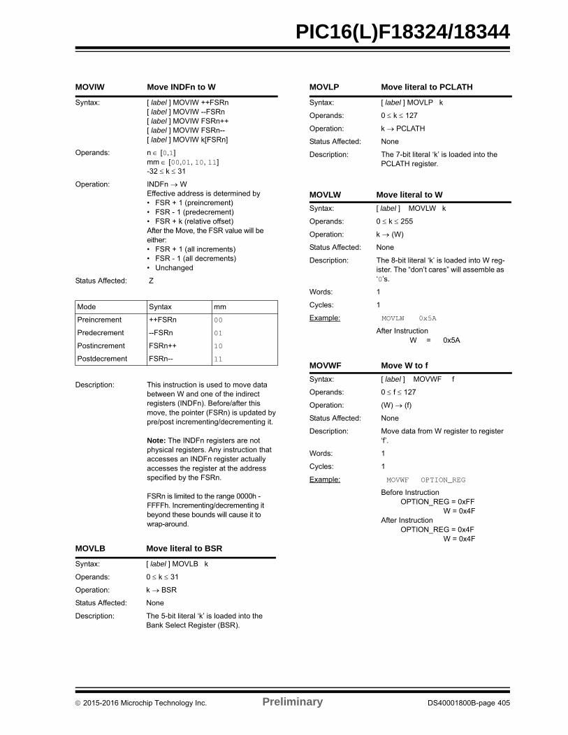
PIC16(L)F18324/18344
MOVIW Move INDFn to W
Syntax: [ label ] MOVIW ++FSRn[ label ] MOVIW --FSRn[ label ] MOVIW FSRn++[ label ] MOVIW FSRn--[ label ] MOVIW k[FSRn]
Operands: n [0,1]mm [00,01, 10, 11]-32 k 31
Operation: INDFn WEffective address is determined by• FSR + 1 (preincrement)• FSR - 1 (predecrement)• FSR + k (relative offset)After the Move, the FSR value will be either:• FSR + 1 (all increments)• FSR - 1 (all decrements)• Unchanged
Status Affected: Z
Mode Syntax mm
Preincrement ++FSRn 00
Predecrement --FSRn 01
Postincrement FSRn++ 10
Postdecrement FSRn-- 11
Description: This instruction is used to move data between W and one of the indirect registers (INDFn). Before/after this move, the pointer (FSRn) is updated by pre/post incrementing/decrementing it.
Note: The INDFn registers are not physical registers. Any instruction that accesses an INDFn register actually accesses the register at the address specified by the FSRn.
FSRn is limited to the range 0000h - FFFFh. Incrementing/decrementing it beyond these bounds will cause it to wrap-around.
MOVLB Move literal to BSR
Syntax: [ label ] MOVLB k
Operands: 0 k 31
Operation: k BSR
Status Affected: None
Description: The 5-bit literal ‘k’ is loaded into the Bank Select Register (BSR).
MOVLP Move literal to PCLATH
Syntax: [ label ] MOVLP k
Operands: 0 k 127
Operation: k PCLATH
Status Affected: None
Description: The 7-bit literal ‘k’ is loaded into the PCLATH register.
MOVLW Move literal to W
Syntax: [ label ] MOVLW k
Operands: 0 k 255
Operation: k (W)
Status Affected: None
Description: The 8-bit literal ‘k’ is loaded into W reg-ister. The “don’t cares” will assemble as ‘0’s.
Words: 1
Cycles: 1
Example: MOVLW 0x5A
After InstructionW = 0x5A
MOVWF Move W to f
Syntax: [ label ] MOVWF f
Operands: 0 f 127
Operation: (W) (f)
Status Affected: None
Description: Move data from W register to register ‘f’.
Words: 1
Cycles: 1
Example: MOVWF OPTION_REG
Before InstructionOPTION_REG = 0xFF
W = 0x4FAfter Instruction
OPTION_REG = 0x4F W = 0x4F
2015-2016 Microchip Technology Inc. Preliminary DS40001800B-page 405
PIC16(L)F18324/18344
MOVWI Move W to INDFn
Syntax: [ label ] MOVWI ++FSRn[ label ] MOVWI --FSRn[ label ] MOVWI FSRn++[ label ] MOVWI FSRn--[ label ] MOVWI k[FSRn]
Operands: n [0,1]mm [00,01, 10, 11]-32 k 31
Operation: W INDFnEffective address is determined by• FSR + 1 (preincrement)• FSR - 1 (predecrement)• FSR + k (relative offset)After the Move, the FSR value will be either:• FSR + 1 (all increments)• FSR - 1 (all decrements)Unchanged
Status Affected: None
Mode Syntax mm
Preincrement ++FSRn 00
Predecrement --FSRn 01
Postincrement FSRn++ 10
Postdecrement FSRn-- 11
Description: This instruction is used to move data between W and one of the indirect registers (INDFn). Before/after this move, the pointer (FSRn) is updated by pre/post incrementing/decrementing it.
Note: The INDFn registers are not physical registers. Any instruction that accesses an INDFn register actually accesses the register at the address specified by the FSRn.
FSRn is limited to the range 0000h-FFFFh. Incrementing/decrementing it beyond these bounds will cause it to wrap-around.
The increment/decrement operation on FSRn WILL NOT affect any Status bits.
NOP No Operation
Syntax: [ label ] NOP
Operands: None
Operation: No operation
Status Affected: None
Description: No operation.
Words: 1
Cycles: 1
Example: NOP
RESET Software Reset
Syntax: [ label ] RESET
Operands: None
Operation: Execute a device Reset. Resets the RI flag of the PCON register.
Status Affected: None
Description: This instruction provides a way to execute a hardware Reset by software.
RETFIE Return from Interrupt
Syntax: [ label ] RETFIE k
Operands: None
Operation: TOS PC,1 GIE
Status Affected: None
Description: Return from Interrupt. Stack is POPed and Top-of-Stack (TOS) is loaded in the PC. Interrupts are enabled by setting Global Interrupt Enable bit, GIE (INTCON<7>). This is a 2-cycle instruction.
Words: 1
Cycles: 2
Example: RETFIE
After InterruptPC = TOSGIE = 1
2015-2016 Microchip Technology Inc. Preliminary DS40001800B-page 406
PIC16(L)F18324/18344
RETLW Return with literal in W
Syntax: [ label ] RETLW k
Operands: 0 k 255
Operation: k (W); TOS PC
Status Affected: None
Description: The W register is loaded with the 8-bit literal ‘k’. The program counter is loaded from the top of the stack (the return address). This is a 2-cycle instruction.
Words: 1
Cycles: 2
Example:
TABLE
CALL TABLE;W contains table;offset value
• ;W now has table value••ADDWF PC ;W = offsetRETLW k1 ;Begin tableRETLW k2 ;•••RETLW kn ; End of table
Before InstructionW = 0x07
After InstructionW = value of k8
RETURN Return from Subroutine
Syntax: [ label ] RETURN
Operands: None
Operation: TOS PC
Status Affected: None
Description: Return from subroutine. The stack is POPed and the top of the stack (TOS) is loaded into the program counter. This is a 2-cycle instruction.
RLF Rotate Left f through Carry
Syntax: [ label ] RLF f,d
Operands: 0 f 127d [0,1]
Operation: See description below
Status Affected: C
Description: The contents of register ‘f’ are rotated one bit to the left through the Carry flag. If ‘d’ is ‘0’, the result is placed in the W register. If ‘d’ is ‘1’, the result is stored back in register ‘f’.
Words: 1
Cycles: 1
Example: RLF REG1,0
Before InstructionREG1 = 1110 0110C = 0
After InstructionREG1 = 1110 0110W = 1100 1100C = 1
RRF Rotate Right f through Carry
Syntax: [ label ] RRF f,d
Operands: 0 f 127d [0,1]
Operation: See description below
Status Affected: C
Description: The contents of register ‘f’ are rotated one bit to the right through the Carry flag. If ‘d’ is ‘0’, the result is placed in the W register. If ‘d’ is ‘1’, the result is placed back in register ‘f’.
Register fC
Register fC
2015-2016 Microchip Technology Inc. Preliminary DS40001800B-page 407
PIC16(L)F18324/18344
SLEEP Enter Sleep mode
Syntax: [ label ] SLEEP
Operands: None
Operation: 00h WDT,0 WDT prescaler,1 TO,0 PD
Status Affected: TO, PD
Description: The power-down Status bit, PD is cleared. Time-out Status bit, TO is set. Watchdog Timer and its prescaler are cleared.See Section 9.3 “Sleep Mode” for more information.
SUBLW Subtract W from literal
Syntax: [ label ] SUBLW k
Operands: 0 k 255
Operation: k - (W) W)
Status Affected: C, DC, Z
Description: The W register is subtracted (2’s complement method) from the 8-bit literal ‘k’. The result is placed in the W register.
C = 0 W k
C = 1 W k
DC = 0 W<3:0> k<3:0>
DC = 1 W<3:0> k<3:0>
SUBWF Subtract W from f
Syntax: [ label ] SUBWF f,d
Operands: 0 f 127d [0,1]
Operation: (f) - (W) destination)
Status Affected: C, DC, Z
Description: Subtract (2’s complement method) W register from register ‘f’. If ‘d’ is ‘0’, the result is stored in the W register. If ‘d’ is ‘1’, the result is stored back in register ‘f.
SUBWFB Subtract W from f with Borrow
Syntax: SUBWFB f ,d
Operands: 0 f 127d [0,1]
Operation: (f) – (W) – (B) dest
Status Affected: C, DC, Z
Description: Subtract W and the BORROW flag (CARRY) from register ‘f’ (2’s complement method). If ‘d’ is ‘0’, the result is stored in W. If ‘d’ is ‘1’, the result is stored back in register ‘f’.
SWAPF Swap Nibbles in f
Syntax: [ label ] SWAPF f,d
Operands: 0 f 127d [0,1]
Operation: (f<3:0>) (destination<7:4>),(f<7:4>) (destination<3:0>)
Status Affected: None
Description: The upper and lower nibbles of register ‘f’ are exchanged. If ‘d’ is ‘0’, the result is placed in the W register. If ‘d’ is ‘1’, the result is placed in register ‘f’.
C = 0 W f
C = 1 W f
DC = 0 W<3:0> f<3:0>
DC = 1 W<3:0> f<3:0>
2015-2016 Microchip Technology Inc. Preliminary DS40001800B-page 408
PIC16(L)F18324/18344
TRIS Load TRIS Register with W
Syntax: [ label ] TRIS f
Operands: 5 f 7
Operation: (W) TRIS register ‘f’
Status Affected: None
Description: Move data from W register to TRIS register.When ‘f’ = 5, TRISA is loaded.When ‘f’ = 6, TRISB is loaded.When ‘f’ = 7, TRISC is loaded.
XORLW Exclusive OR literal with W
Syntax: [ label ] XORLW k
Operands: 0 k 255
Operation: (W) .XOR. k W)
Status Affected: Z
Description: The contents of the W register are XOR’ed with the 8-bit literal ‘k’. The result is placed in the W register.
XORWF Exclusive OR W with f
Syntax: [ label ] XORWF f,d
Operands: 0 f 127d [0,1]
Operation: (W) .XOR. (f) destination)
Status Affected: Z
Description: Exclusive OR the contents of the W register with register ‘f’. If ‘d’ is ‘0’, the result is stored in the W register. If ‘d’ is ‘1’, the result is stored back in register ‘f’.
2015-2016 Microchip Technology Inc. Preliminary DS40001800B-page 409
PIC16(L)F18324/18344
35.0 ELECTRICAL SPECIFICATIONS
35.1 Absolute Maximum Ratings(†)
Ambient temperature under bias...................................................................................................... -40°C to +125°C
Storage temperature ........................................................................................................................ -65°C to +150°C
Voltage on pins with respect to VSS
on VDD pin
PIC16F18324/18344 ................................................................................................. -0.3V to +6.5V
PIC16LF18324/18344 ............................................................................................... -0.3V to +4.0V
on MCLR pin ........................................................................................................................... -0.3V to +9.0V
on all other pins ............................................................................................................ -0.3V to (VDD + 0.3V)
Maximum current
on VSS pin(1)
-40°C TA +85°C .............................................................................................................. 250 mA
+85°C TA +125°C ............................................................................................................. 85 mA
on VDD pin(1)
-40°C TA +85°C .............................................................................................................. 250 mA
+85°C TA +125°C ............................................................................................................. 85 mA
on any I/O pin ..................................................................................................................................... 50 mA
Clamp current, IK (VPIN < 0 or VPIN > VDD) ................................................................................................... 20 mA
Total power dissipation(2) .............................................................................................................................. 800 mW
Note 1: Maximum current rating requires even load distribution across I/O pins. Maximum current rating may be limited by the device package power dissipation characterizations, see Table 35-3 to calculate device specifications.
2: Power dissipation is calculated as follows:
PDIS = VDD x IDD – ∑ IOH + ∑ (VDD – VOH) x IOH + ∑(VOL x IOL).
† NOTICE: Stresses above those listed under “Absolute Maximum Ratings” may cause permanent damage to thedevice. This is a stress rating only and functional operation of the device at those or any other conditions above thoseindicated in the operation listings of this specification is not implied. Exposure above maximum rating conditions forextended periods may affect device reliability.
2015-2016 Microchip Technology Inc. Preliminary DS40001800B-page 410
PIC16(L)F18324/18344
35.2 Standard Operating Conditions
The standard operating conditions for any device are defined as:
Operating Voltage: VDDMIN VDD VDDMAX
Operating Temperature: TA_MIN TA TA_MAX
VDD — Operating Supply Voltage(1)
PIC16LF18324/18344
VDDMIN (Fosc 16 MHz) ......................................................................................................... +1.8V
VDDMIN (Fosc 32 MHz) ......................................................................................................... +2.5V
VDDMAX .................................................................................................................................... +3.6V
PIC16F18324/18344
VDDMIN (Fosc 16 MHz) ......................................................................................................... +2.3V
VDDMIN (Fosc 32 MHz) ......................................................................................................... +2.5V
VDDMAX .................................................................................................................................... +5.5V
TA — Operating Ambient Temperature Range
Industrial Temperature
TA_MIN...................................................................................................................................... -40°C
TA_MAX.................................................................................................................................... +85°C
Extended Temperature
TA_MIN...................................................................................................................................... -40°C
TA_MAX.................................................................................................................................. +125°C
Note 1: See Parameter D002, DC Characteristics: Supply Voltage.
2015-2016 Microchip Technology Inc. Preliminary DS40001800B-page 411
PIC16(L)F18324/18344
FIGURE 35-1: VOLTAGE FREQUENCY GRAPH, -40°C TA +125°C, PIC16F18324/18344 ONLY
FIGURE 35-2: VOLTAGE FREQUENCY GRAPH, -40°C TA +125°C, PIC16LF18324/18344 ONLY
0
2.5
Frequency (MHz)
VD
D (
V)
4 3210 16
5.5
2.3
Note 1: The shaded region indicates the permissible combinations of voltage and frequency.2: Refer to Table 35-7 for each Oscillator mode’s supported frequencies.
1.8
0
2.5
Frequency (MHz)
VD
D (
V)
4 3210 16
3.6
Note 1: The shaded region indicates the permissible combinations of voltage and frequency.2: Refer to Table 35-7 for each Oscillator mode’s supported frequencies.
2015-2016 Microchip Technology Inc. Preliminary DS40001800B-page 412
PIC16(L)F18324/18344
35.3 DC Characteristics
TABLE 35-1: SUPPLY VOLTAGE
PIC16LF18324/18344 Standard Operating Conditions (unless otherwise stated)
PIC16F18324/18344 Standard Operating Conditions (unless otherwise stated)
Param. No.
Sym. Characteristic Min. Typ.† Max. Units Conditions
Supply Voltage
D002 VDD 1.82.5
——
3.63.6
VV
FOSC 16 MHzFOSC > 16 MHz
D002 VDD 2.32.5
——
5.55.5
VV
FOSC 16 MHz:FOSC > 16 MHz
RAM Data Retention(1)
D003 VDR 1.5 — — V Device in Sleep mode
D003 VDR 1.7 — — V Device in Sleep mode
Power-on Reset Release Voltage(2)
D004 VPOR — 1.6 — V BOR and LPBOR disabled(3)
D004 VPOR — 1.6 — V BOR and LPBOR disabled(3)
Power-on Reset ReARM Voltage(2)
D005 VPORR — 0.8 — V BOR and LPBOR disabled(3)
D005 VPORR — 1.5 — V BOR and LPBOR disabled(3)
VDD Rise Rate to ensure Internal Power-on Reset Signal(2)
D006 SVDD 0.05 — — V/ms BOR and LPBOR disabled(3)
D006 SVDD 0.05 — — V/ms BOR and LPBOR disabled(3)
† Data in “Typ.” column is at 3.0V, 25°C unless otherwise stated. These parameters are for design guidance only and are not tested.
Note 1: This is the limit to which VDD can be lowered in Sleep mode or during a device Reset, without losing RAM data.
2: See Figure 35-3.
3: See Table 35-11 for BOR and LPBOR trip point information.
2015-2016 Microchip Technology Inc. Preliminary DS40001800B-page 413
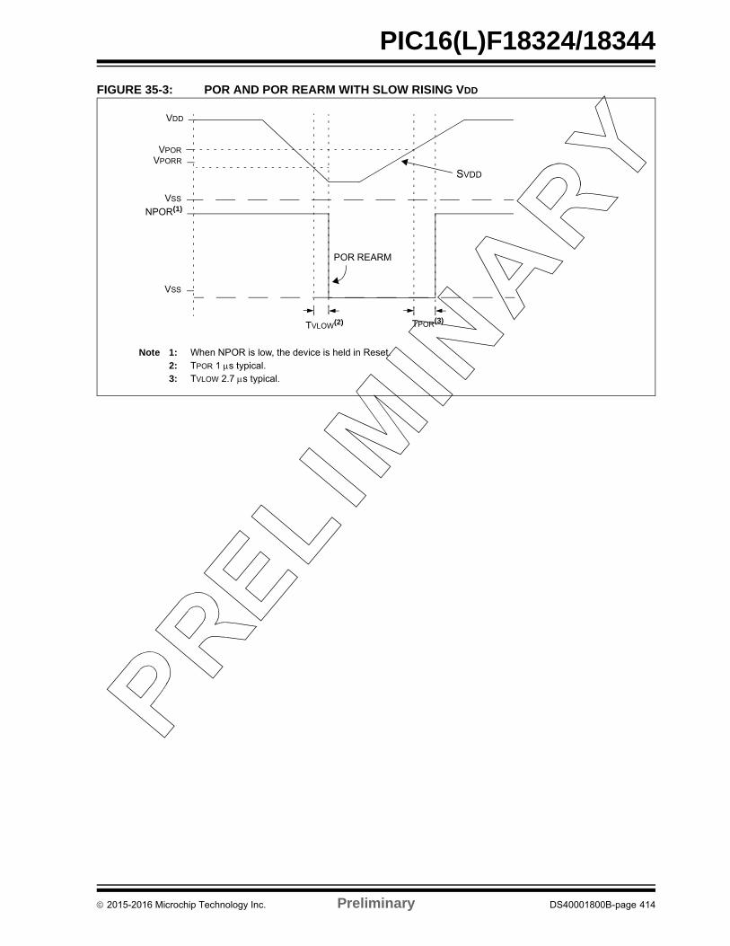
PIC16(L)F18324/18344
FIGURE 35-3: POR AND POR REARM WITH SLOW RISING VDD
VDD
VPOR
VPORR
VSS
VSS
NPOR(1)
TPOR(3)
POR REARM
TVLOW(2)
SVDD
Note 1: When NPOR is low, the device is held in Reset.2: TPOR 1 s typical.3: TVLOW 2.7 s typical.
2015-2016 Microchip Technology Inc. Preliminary DS40001800B-page 414
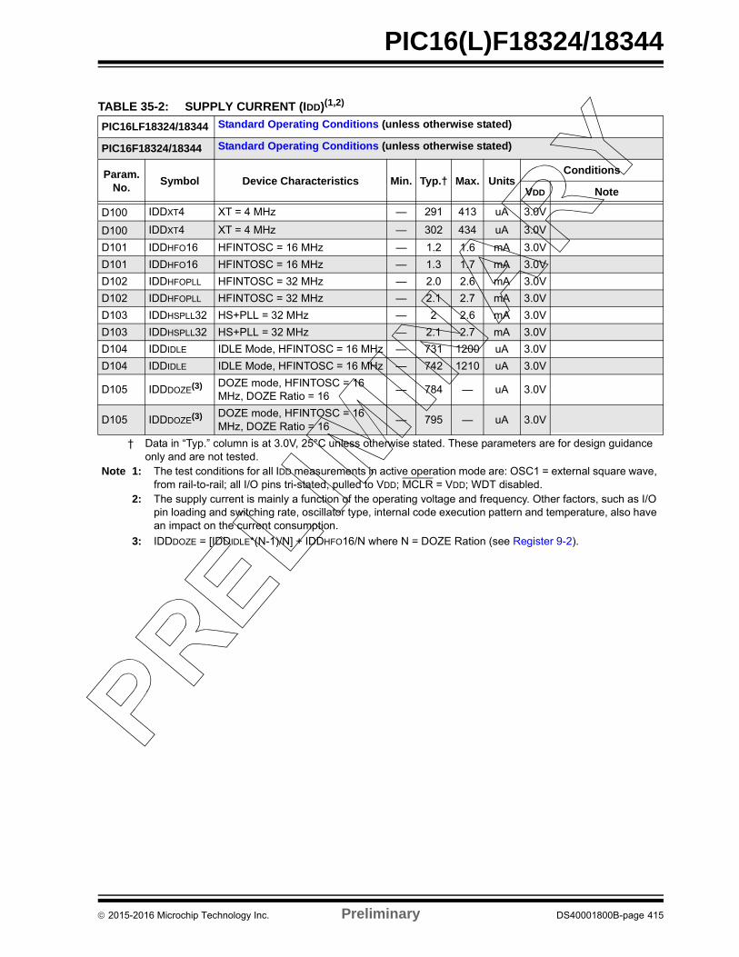
PIC16(L)F18324/18344
TABLE 35-2: SUPPLY CURRENT (IDD)(1,2)
PIC16LF18324/18344 Standard Operating Conditions (unless otherwise stated)
PIC16F18324/18344 Standard Operating Conditions (unless otherwise stated)
Param.No.
Symbol Device Characteristics Min. Typ.† Max. UnitsConditions
VDD Note
D100 IDDXT4 XT = 4 MHz — 291 413 uA 3.0V
D100 IDDXT4 XT = 4 MHz — 302 434 uA 3.0V
D101 IDDHFO16 HFINTOSC = 16 MHz — 1.2 1.6 mA 3.0V
D101 IDDHFO16 HFINTOSC = 16 MHz — 1.3 1.7 mA 3.0V
D102 IDDHFOPLL HFINTOSC = 32 MHz — 2.0 2.6 mA 3.0V
D102 IDDHFOPLL HFINTOSC = 32 MHz — 2.1 2.7 mA 3.0V
D103 IDDHSPLL32 HS+PLL = 32 MHz — 2 2.6 mA 3.0V
D103 IDDHSPLL32 HS+PLL = 32 MHz — 2.1 2.7 mA 3.0V
D104 IDDIDLE IDLE Mode, HFINTOSC = 16 MHz — 731 1200 uA 3.0V
D104 IDDIDLE IDLE Mode, HFINTOSC = 16 MHz — 742 1210 uA 3.0V
D105 IDDDOZE(3) DOZE mode, HFINTOSC = 16 MHz, DOZE Ratio = 16
— 784 — uA 3.0V
D105 IDDDOZE(3) DOZE mode, HFINTOSC = 16 MHz, DOZE Ratio = 16
— 795 — uA 3.0V
† Data in “Typ.” column is at 3.0V, 25°C unless otherwise stated. These parameters are for design guidance only and are not tested.
Note 1: The test conditions for all IDD measurements in active operation mode are: OSC1 = external square wave, from rail-to-rail; all I/O pins tri-stated, pulled to VDD; MCLR = VDD; WDT disabled.
2: The supply current is mainly a function of the operating voltage and frequency. Other factors, such as I/O pin loading and switching rate, oscillator type, internal code execution pattern and temperature, also have an impact on the current consumption.
3: IDDDOZE = [IDDIDLE*(N-1)/N] + IDDHFO16/N where N = DOZE Ration (see Register 9-2).
2015-2016 Microchip Technology Inc. Preliminary DS40001800B-page 415
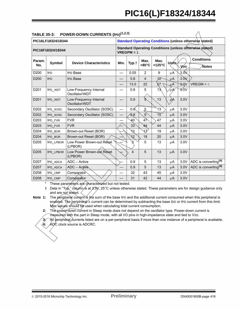
PIC16(L)F18324/18344
4)
4)
ly
.
le.
TABLE 35-3: POWER-DOWN CURRENTS (IPD)(1,2,3)
PIC16LF18324/18344 Standard Operating Conditions (unless otherwise stated)
PIC16F18324/18344Standard Operating Conditions (unless otherwise stated)VREGPM = 1
Param.No.
Symbol Device Characteristics Min. Typ.†Max.
+85°CMax.
+125°CUnits
Conditions
VDD Notes
D200 IPD IPD Base — 0.05 2 9 A 3.0V
D200 IPD IPD Base — 0.8 4 12 A 3.0V
— 13.0 22 27 A 3.0V VREGM = 0
D201 IPD_WDT Low-Frequency Internal Oscillator/WDT
— 0.8 5 13 A 3.0V
D201 IPD_WDT Low-Frequency Internal Oscillator/WDT
— 0.9 5 13 A 3.0V
D202 IPD_SOSC Secondary Oscillator (SOSC) — 0.6 5 13 A 3.0V
D202 IPD_SOSC Secondary Oscillator (SOSC) — 0.8 9 15 A 3.0V
D203 IPD_FVR FVR — 40 47 47 A 3.0V
D203 IPD_FVR FVR — 33 44 44 A 3.0V
D204 IPD_BOR Brown-out Reset (BOR) — 12 17 19 A 3.0V
D204 IPD_BOR Brown-out Reset (BOR) — 12 18 20 A 3.0V
D205 IPD_LPBOR Low Power Brown-out Reset (LPBOR)
— 3 5 13 A 3.0V
D205 IPD_LPBOR Low Power Brown-out Reset (LPBOR)
— 4 5 13 A 3.0V
D207 IPD_ADCA ADC – Active — 0.9 5 13 A 3.0V ADC is converting(
D207 IPD_ADCA ADC – Active — 0.9 5 13 A 3.0V ADC is converting(
D208 IPD_CMP Comparator — 32 43 45 A 3.0V
D208 IPD_CMP Comparator — 31 42 44 A 3.0V
* These parameters are characterized but not tested.† Data in “Typ.” column is at 3.0V, 25°C unless otherwise stated. These parameters are for design guidance on
and are not tested.Note 1: The peripheral current is the sum of the base IPD and the additional current consumed when this peripheral is
enabled. The peripheral current can be determined by subtracting the base IDD or IPD current from this limitMax values should be used when calculating total current consumption.
2: The power-down current in Sleep mode does not depend on the oscillator type. Power-down current is measured with the part in Sleep mode, with all I/O pins in high-impedance state and tied to VSS.
3: All peripheral currents listed are on a per-peripheral basis if more than one instance of a peripheral is availab4: ADC clock source is ADCRC.
2015-2016 Microchip Technology Inc. Preliminary DS40001800B-page 416

PIC16(L)F18324/18344
TABLE 35-4: I/O PORTS
DC CHARACTERISTICS Standard Operating Conditions (unless otherwise stated)
Param.No.
Sym. Characteristic Min. Typ.† Max. Units Conditions
VIL Input Low Voltage
I/O Port:
D300 with TTL buffer — — 0.8 V 4.5V VDD 5.5V
D301 — — 0.15 VDD V 1.8V VDD 4.5V
D302 with Schmitt Trigger buffer — — 0.2 VDD V 2.0V VDD 5.5V
D303 with I2C levels — — 0.3 VDD V
D304 with SM Bus levels — — 0.8 V 2.7V VDD 5.5V
D305 MCLR — — 0.2 VDD V
VIH Input High Voltage
I/O Port:
D320 with TTL buffer 2.0 — — V 4.5V VDD 5.5V
D321 0.25 VDD + 0.8 — — V 1.8V VDD 4.5V
D322 with Schmitt Trigger buffer 0.8 VDD — — V 2.0V VDD 5.5V
D323 with I2C levels 0.7 VDD — — V
D324 with SMBus levels 2.1 — — V 2.7V VDD 5.5V
D325 MCLR 0.7 VDD — — V
IIL Input Leakage Current(2)
D340 I/O Ports — ± 5 ± 125 nA VSS VPIN VDD, Pin at high-impedance, 85°C
D341 — ± 5 ± 1000 nA VSS VPIN VDD, Pin at high-impedance, 125°C
D342 MCLR(2) — ± 50 ± 200 nA VSS VPIN VDD, Pin at high-impedance, 85°C
IPUR Weak Pull-up Current
D350 25 120 200 A VDD = 3.0V, VPIN = VSS
VOL Output Low Voltage(4)
D360 I/O ports — — 0.6 V IOL = 10.0 mA, VDD = 3.0V
VOH Output High Voltage(4)
D370 I/O ports VDD - 0.7 — — V IOH = 6.0 mA, VDD = 3.0V
D380 CIO All I/O pins — 5 50 pF
* These parameters are characterized but not tested.† Data in “Typ.” column is at 3.0V, 25°C unless otherwise stated. These parameters are for design guidance
only and are not tested.Note 1: Negative current is defined as current sourced by the pin.
2: The leakage current on the MCLR pin is strongly dependent on the applied voltage level. The specified levels represent normal operating conditions. Higher leakage current may be measured at different input voltages.
2015-2016 Microchip Technology Inc. Preliminary DS40001800B-page 417
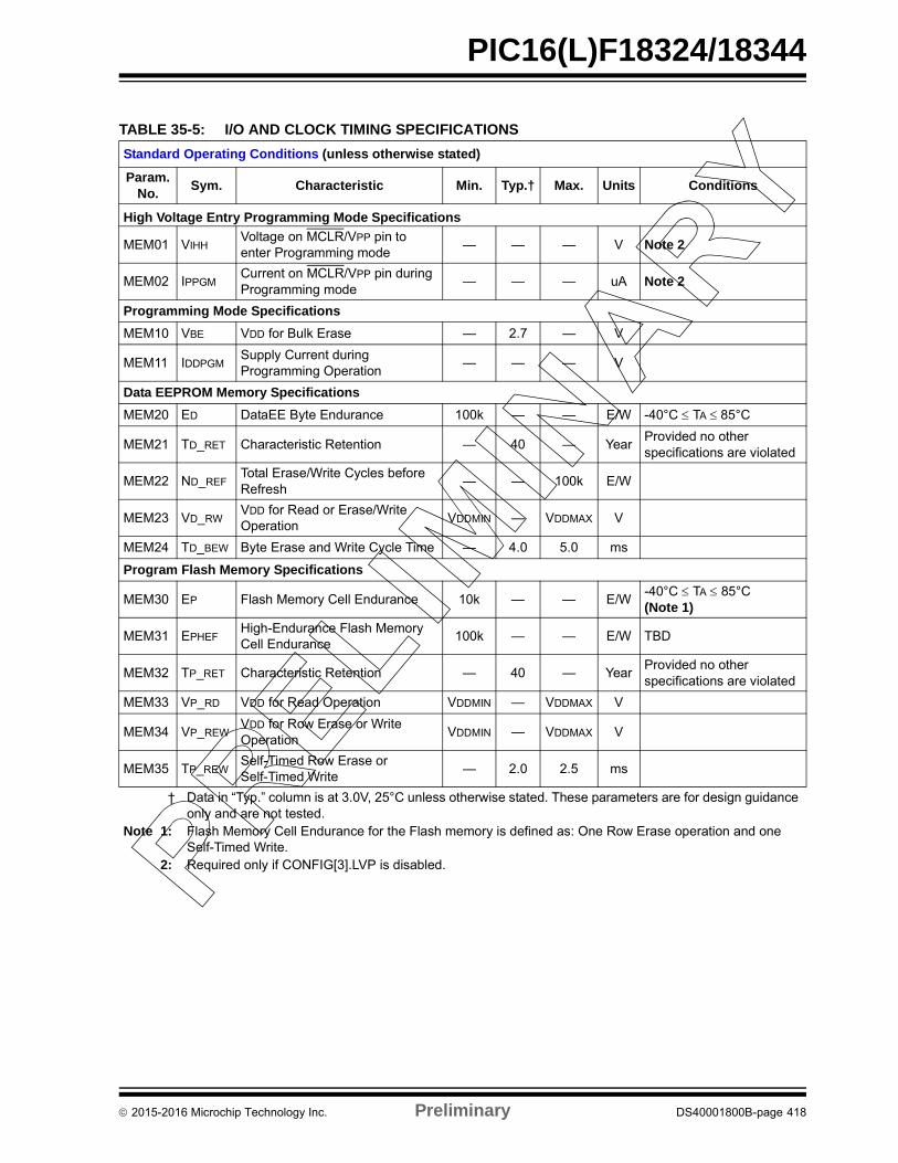
PIC16(L)F18324/18344
TABLE 35-5: I/O AND CLOCK TIMING SPECIFICATIONS
Standard Operating Conditions (unless otherwise stated)
Param.No.
Sym. Characteristic Min. Typ.† Max. Units Conditions
High Voltage Entry Programming Mode Specifications
MEM01 VIHHVoltage on MCLR/VPP pin to enter Programming mode
— — — V Note 2
MEM02 IPPGMCurrent on MCLR/VPP pin during Programming mode
— — — uA Note 2
Programming Mode Specifications
MEM10 VBE VDD for Bulk Erase — 2.7 — V
MEM11 IDDPGMSupply Current during Programming Operation
— — — V
Data EEPROM Memory Specifications
MEM20 ED DataEE Byte Endurance 100k — — E/W -40°C TA 85°C
MEM21 TD_RET Characteristic Retention — 40 — YearProvided no other specifications are violated
MEM22 ND_REFTotal Erase/Write Cycles before Refresh
— — 100k E/W
MEM23 VD_RWVDD for Read or Erase/Write Operation
VDDMIN — VDDMAX V
MEM24 TD_BEW Byte Erase and Write Cycle Time — 4.0 5.0 ms
Program Flash Memory Specifications
MEM30 EP Flash Memory Cell Endurance 10k — — E/W-40°C TA 85°C(Note 1)
MEM31 EPHEFHigh-Endurance Flash Memory Cell Endurance
100k — — E/W TBD
MEM32 TP_RET Characteristic Retention — 40 — YearProvided no other specifications are violated
MEM33 VP_RD VDD for Read Operation VDDMIN — VDDMAX V
MEM34 VP_REWVDD for Row Erase or Write Operation
VDDMIN — VDDMAX V
MEM35 TP_REWSelf-Timed Row Erase or Self-Timed Write
— 2.0 2.5 ms
† Data in “Typ.” column is at 3.0V, 25°C unless otherwise stated. These parameters are for design guidance only and are not tested.
Note 1: Flash Memory Cell Endurance for the Flash memory is defined as: One Row Erase operation and one Self-Timed Write.
2: Required only if CONFIG[3].LVP is disabled.
2015-2016 Microchip Technology Inc. Preliminary DS40001800B-page 418
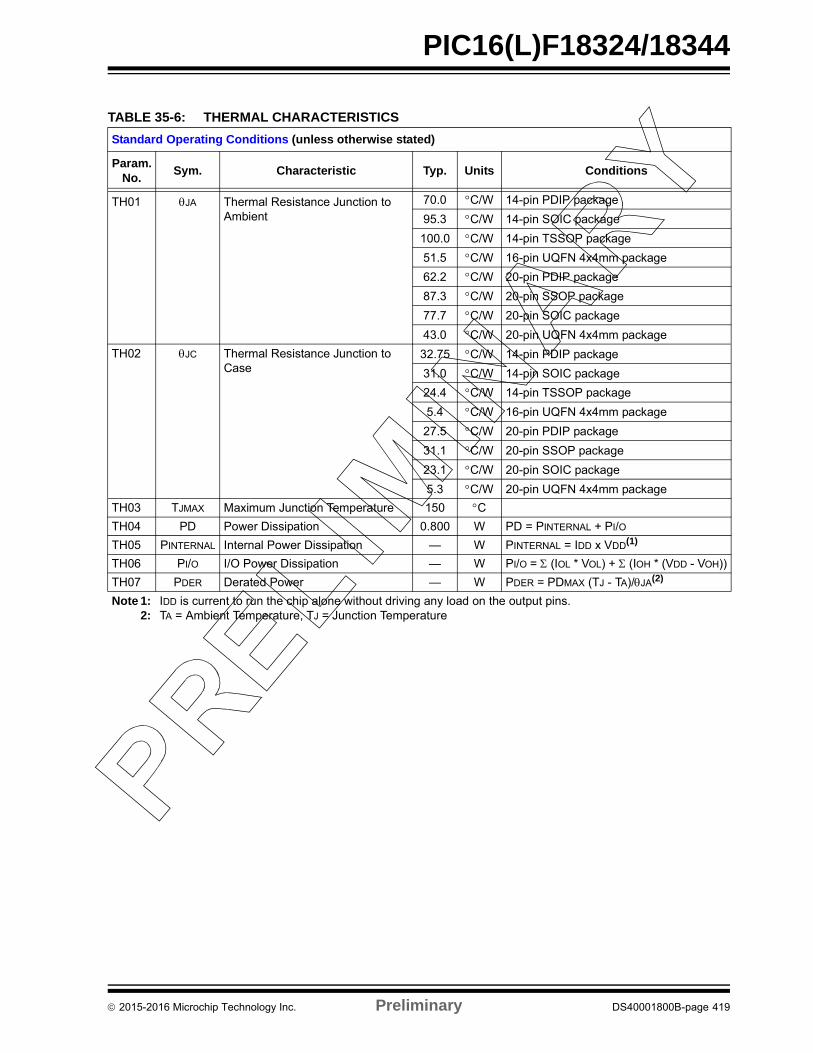
PIC16(L)F18324/18344
TABLE 35-6: THERMAL CHARACTERISTICS
Standard Operating Conditions (unless otherwise stated)
Param.No.
Sym. Characteristic Typ. Units Conditions
TH01 JA Thermal Resistance Junction to Ambient
70.0 C/W 14-pin PDIP package
95.3 C/W 14-pin SOIC package
100.0 C/W 14-pin TSSOP package
51.5 C/W 16-pin UQFN 4x4mm package
62.2 C/W 20-pin PDIP package
87.3 C/W 20-pin SSOP package
77.7 C/W 20-pin SOIC package
43.0 C/W 20-pin UQFN 4x4mm package
TH02 JC Thermal Resistance Junction to Case
32.75 C/W 14-pin PDIP package
31.0 C/W 14-pin SOIC package
24.4 C/W 14-pin TSSOP package
5.4 C/W 16-pin UQFN 4x4mm package
27.5 C/W 20-pin PDIP package
31.1 C/W 20-pin SSOP package
23.1 C/W 20-pin SOIC package
5.3 C/W 20-pin UQFN 4x4mm package
TH03 TJMAX Maximum Junction Temperature 150 C
TH04 PD Power Dissipation 0.800 W PD = PINTERNAL + PI/O
TH05 PINTERNAL Internal Power Dissipation — W PINTERNAL = IDD x VDD(1)
TH06 PI/O I/O Power Dissipation — W PI/O = (IOL * VOL) + (IOH * (VDD - VOH))
TH07 PDER Derated Power — W PDER = PDMAX (TJ - TA)/JA(2)
Note 1: IDD is current to run the chip alone without driving any load on the output pins.2: TA = Ambient Temperature, TJ = Junction Temperature
2015-2016 Microchip Technology Inc. Preliminary DS40001800B-page 419
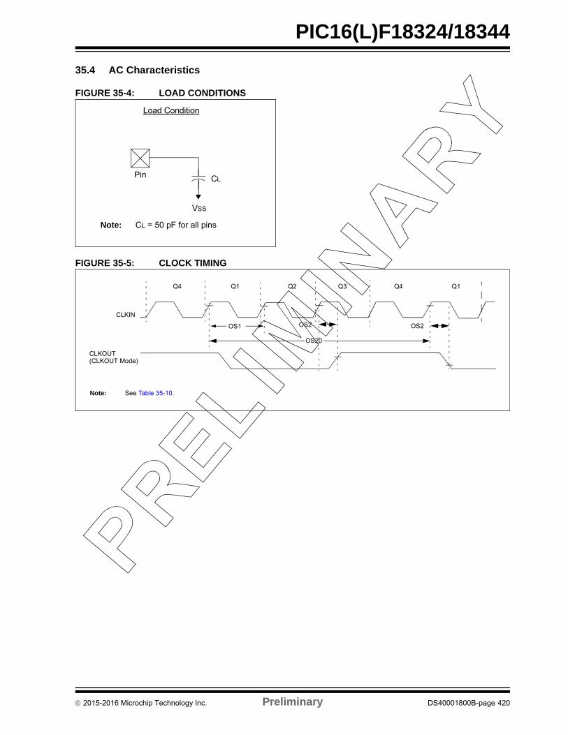
PIC16(L)F18324/18344
35.4 AC Characteristics
FIGURE 35-4: LOAD CONDITIONS
FIGURE 35-5: CLOCK TIMING
VSS
CL
Load Condition
Pin
Note: CL = 50 pF for all pins
CLKIN
CLKOUT
Q4 Q1 Q2 Q3 Q4 Q1
OS1
OS20
(CLKOUT Mode)
OS2OS2
Note: See Table 35-10.
2015-2016 Microchip Technology Inc. Preliminary DS40001800B-page 420
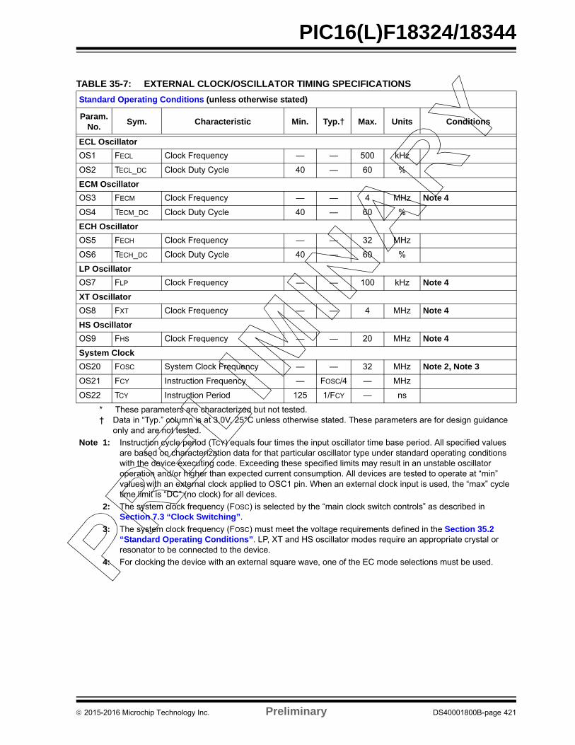
PIC16(L)F18324/18344
TABLE 35-7: EXTERNAL CLOCK/OSCILLATOR TIMING SPECIFICATIONS
Standard Operating Conditions (unless otherwise stated)
Param.No.
Sym. Characteristic Min. Typ.† Max. Units Conditions
ECL Oscillator
OS1 FECL Clock Frequency — — 500 kHz
OS2 TECL_DC Clock Duty Cycle 40 — 60 %
ECM Oscillator
OS3 FECM Clock Frequency — — 4 MHz Note 4
OS4 TECM_DC Clock Duty Cycle 40 — 60 %
ECH Oscillator
OS5 FECH Clock Frequency — — 32 MHz
OS6 TECH_DC Clock Duty Cycle 40 — 60 %
LP Oscillator
OS7 FLP Clock Frequency — — 100 kHz Note 4
XT Oscillator
OS8 FXT Clock Frequency — — 4 MHz Note 4
HS Oscillator
OS9 FHS Clock Frequency — — 20 MHz Note 4
System Clock
OS20 FOSC System Clock Frequency — — 32 MHz Note 2, Note 3
OS21 FCY Instruction Frequency — FOSC/4 — MHz
OS22 TCY Instruction Period 125 1/FCY — ns
* These parameters are characterized but not tested.† Data in “Typ.” column is at 3.0V, 25°C unless otherwise stated. These parameters are for design guidance
only and are not tested.
Note 1: Instruction cycle period (TCY) equals four times the input oscillator time base period. All specified values are based on characterization data for that particular oscillator type under standard operating conditions with the device executing code. Exceeding these specified limits may result in an unstable oscillator operation and/or higher than expected current consumption. All devices are tested to operate at “min” values with an external clock applied to OSC1 pin. When an external clock input is used, the “max” cycle time limit is “DC” (no clock) for all devices.
2: The system clock frequency (FOSC) is selected by the “main clock switch controls” as described in Section 7.3 “Clock Switching”.
3: The system clock frequency (FOSC) must meet the voltage requirements defined in the Section 35.2 “Standard Operating Conditions”. LP, XT and HS oscillator modes require an appropriate crystal or resonator to be connected to the device.
4: For clocking the device with an external square wave, one of the EC mode selections must be used.
2015-2016 Microchip Technology Inc. Preliminary DS40001800B-page 421
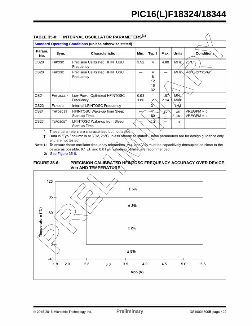
PIC16(L)F18324/18344
FIGURE 35-6: PRECISION CALIBRATED HFINTOSC FREQUENCY ACCURACY OVER DEVICE VDD AND TEMPERATURE
TABLE 35-8: INTERNAL OSCILLATOR PARAMETERS(1)
Standard Operating Conditions (unless otherwise stated)
Param. No.
Sym. Characteristic Min. Typ.† Max. Units Conditions
OS20 FHFOSC Precision Calibrated HFINTOSC Frequency
3.92 4 4.08 MHz 25°C
OS20 FHFOSC Precision Calibrated HFINTOSC Frequency
— 48121632
— MHz -40°C to 125°C
OS21 FHFOSCLP Low-Power Optimized HFINTOSC Frequency
0.931.86
12
1.072.14
MHzMHz
OS23 FLFOSC Internal LFINTOSC Frequency — 31 — kHz
OS24 THFOSCST HFINTOSC Wake-up from Sleep Start-up Time
— 1150
20—
ss
VREGPM = 0VREGPM = 1
OS26 TLFOSCST LFINTOSC Wake-up from Sleep Start-up Time
— 0.2 — ms
* These parameters are characterized but not tested.† Data in “Typ.” column is at 3.0V, 25°C unless otherwise stated. These parameters are for design guidance only
and are not tested.Note 1: To ensure these oscillator frequency tolerances, VDD and VSS must be capacitively decoupled as close to the
device as possible. 0.1 F and 0.01 F values in parallel are recommended.2: See Figure 35-6.
125
2.0
0
60
85
VDD (V)
4.0 5.04.5
Tem
pe
ratu
re (
°C)
2.3 3.0 3.5 5.51.8-40
± 5%
± 2%
± 5%
± 3%
2015-2016 Microchip Technology Inc. Preliminary DS40001800B-page 422
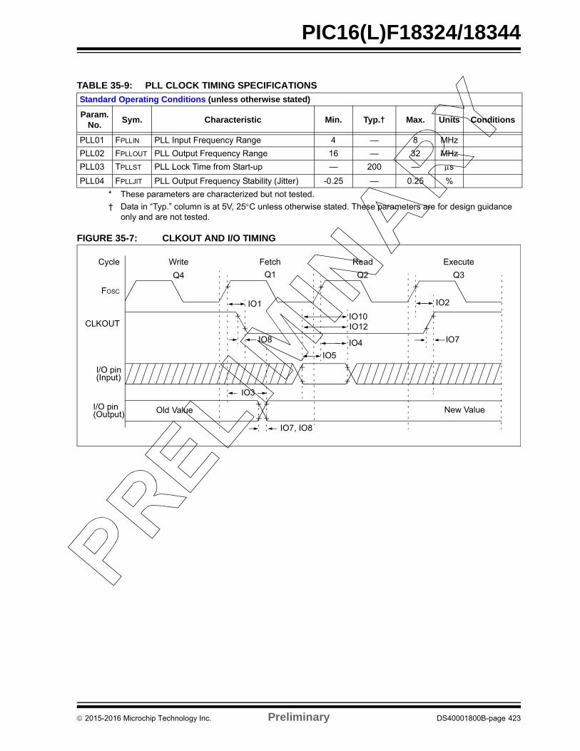
PIC16(L)F18324/18344
FIGURE 35-7: CLKOUT AND I/O TIMING
TABLE 35-9: PLL CLOCK TIMING SPECIFICATIONS
Standard Operating Conditions (unless otherwise stated)
Param. No.
Sym. Characteristic Min. Typ.† Max. Units Conditions
PLL01 FPLLIN PLL Input Frequency Range 4 — 8 MHz
PLL02 FPLLOUT PLL Output Frequency Range 16 — 32 MHz
PLL03 TPLLST PLL Lock Time from Start-up — 200 — s
PLL04 FPLLJIT PLL Output Frequency Stability (Jitter) -0.25 — 0.25 %
* These parameters are characterized but not tested.
† Data in “Typ.” column is at 5V, 25C unless otherwise stated. These parameters are for design guidance only and are not tested.
FOSC
CLKOUT
I/O pin(Input)
I/O pin(Output)
Q4 Q1 Q2 Q3
IO1
IO8
IO3
IO7, IO8
IO10IO12
IO5
IO4
IO2
IO7
Old Value New Value
Write Fetch Read ExecuteCycle
2015-2016 Microchip Technology Inc. Preliminary DS40001800B-page 423

PIC16(L)F18324/18344
TABLE 35-10: CLKOUT AND I/O TIMING PARAMETERS
Standard Operating Conditions (unless otherwise stated)
Param. No.
Sym. Characteristic Min. Typ.† Max. Units Conditions
IO1 TCLKOUTH CLKOUT rising edge delay(rising edge FOSC (Q1 cycle) to falling edge CLKOUT
— — — ns
IO2 TCLKOUTL CLKOUT falling edge delay(rising edge FOSC (Q3 cycle) to rising edge CLKOUT
— — — ns
IO3 TIO_VALID Port output valid time (rising edge FOSC (Q1 cycle) to port valid)
— — — ns
IO4 TIO_SETUP Port input setup time (Setup time before rising edge FOSC - Q2 cycle)
— — — ns
IO5 TIO_HOLD Port input hold time (Hold time after rising edge FOSC - Q2 cycle)
— — — ns
IO6 TIOR_SLREN Port I/O rise time, slew rate enabled — — — ns
IO7 TIOR_SLRDIS Port I/O rise time, slew rate disabled — — — ns
IO8 TIOF_SLREN Port I/O fall time, slew rate enabled — — — ns
IO9 TIOF_SLRDIS Port I/O fall time, slew rate disabled — — — ns
IO10 TINT INT pin high or low time to trigger an interrupt
— — — ns
IO11 TIOC Interrupt-on-Change minimum high or low time to trigger interrupt
— — — ns
* These parameters are characterized but not tested.† Data in “Typ.” column is at 3.0V, 25C unless otherwise stated.
2015-2016 Microchip Technology Inc. Preliminary DS40001800B-page 424
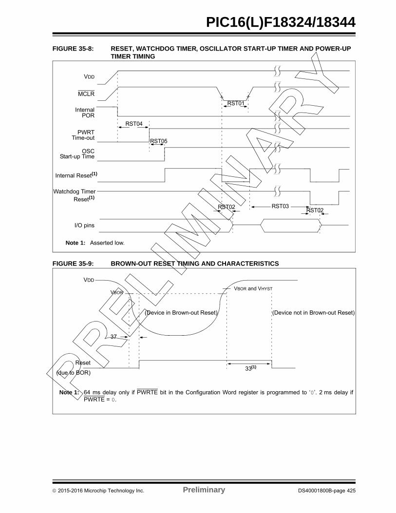
PIC16(L)F18324/18344
FIGURE 35-8: RESET, WATCHDOG TIMER, OSCILLATOR START-UP TIMER AND POWER-UP TIMER TIMING
FIGURE 35-9: BROWN-OUT RESET TIMING AND CHARACTERISTICS
VDD
MCLR
InternalPOR
PWRTTime-out
OSCStart-up Time
Internal Reset(1)
Watchdog Timer
RST01
I/O pins
Reset(1)
Note 1: Asserted low.
RST04
RST05
RST03RST02RST02
VBOR
VDD
(Device in Brown-out Reset) (Device not in Brown-out Reset)
33(1)Reset
(due to BOR)
VBOR and VHYST
37
Note 1: 64 ms delay only if PWRTE bit in the Configuration Word register is programmed to ‘0’. 2 ms delay ifPWRTE = 0.
2015-2016 Microchip Technology Inc. Preliminary DS40001800B-page 425
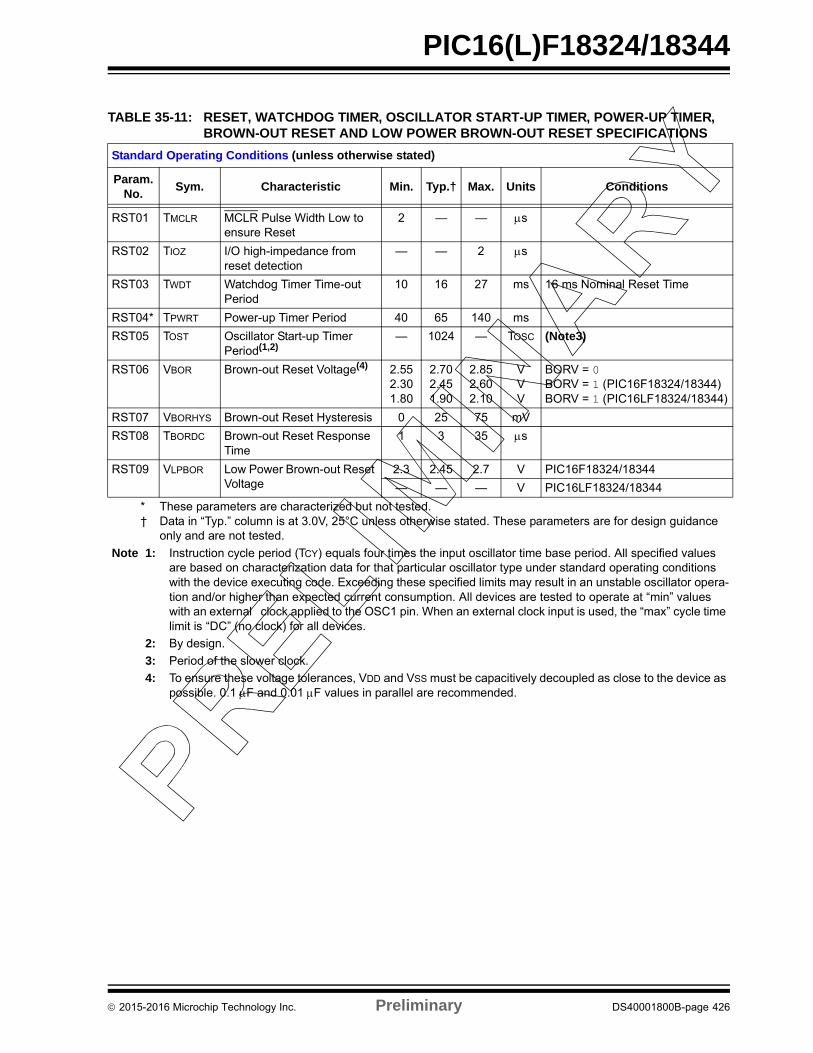
PIC16(L)F18324/18344
TABLE 35-11: RESET, WATCHDOG TIMER, OSCILLATOR START-UP TIMER, POWER-UP TIMER, BROWN-OUT RESET AND LOW POWER BROWN-OUT RESET SPECIFICATIONS
Standard Operating Conditions (unless otherwise stated)
Param. No.
Sym. Characteristic Min. Typ.† Max. Units Conditions
RST01 TMCLR MCLR Pulse Width Low to ensure Reset
2 — — s
RST02 TIOZ I/O high-impedance from reset detection
— — 2 s
RST03 TWDT Watchdog Timer Time-out Period
10 16 27 ms 16 ms Nominal Reset Time
RST04* TPWRT Power-up Timer Period 40 65 140 ms
RST05 TOST Oscillator Start-up Timer Period(1,2)
— 1024 — TOSC (Note3)
RST06 VBOR Brown-out Reset Voltage(4) 2.552.301.80
2.702.451.90
2.852.602.10
VVV
BORV = 0BORV = 1 (PIC16F18324/18344)BORV = 1 (PIC16LF18324/18344)
RST07 VBORHYS Brown-out Reset Hysteresis 0 25 75 mV
RST08 TBORDC Brown-out Reset Response Time
1 3 35 s
RST09 VLPBOR Low Power Brown-out Reset Voltage
2.3 2.45 2.7 V PIC16F18324/18344
— — — V PIC16LF18324/18344
* These parameters are characterized but not tested.† Data in “Typ.” column is at 3.0V, 25°C unless otherwise stated. These parameters are for design guidance
only and are not tested.
Note 1: Instruction cycle period (TCY) equals four times the input oscillator time base period. All specified values are based on characterization data for that particular oscillator type under standard operating conditions with the device executing code. Exceeding these specified limits may result in an unstable oscillator opera-tion and/or higher than expected current consumption. All devices are tested to operate at “min” values with an external clock applied to the OSC1 pin. When an external clock input is used, the “max” cycle time limit is “DC” (no clock) for all devices.
2: By design.
3: Period of the slower clock.
4: To ensure these voltage tolerances, VDD and VSS must be capacitively decoupled as close to the device as possible. 0.1 F and 0.01 F values in parallel are recommended.
2015-2016 Microchip Technology Inc. Preliminary DS40001800B-page 426
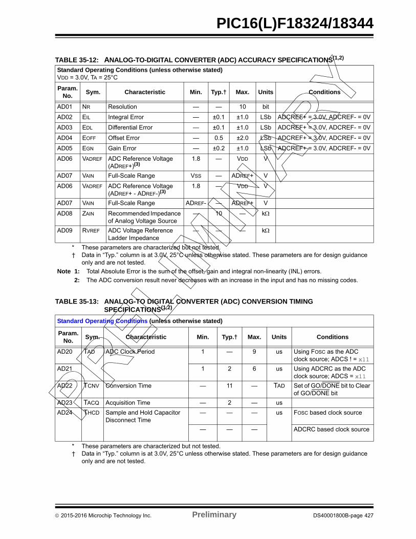
PIC16(L)F18324/18344
TABLE 35-12: ANALOG-TO-DIGITAL CONVERTER (ADC) ACCURACY SPECIFICATIONS(1,2)
Standard Operating Conditions (unless otherwise stated)VDD = 3.0V, TA = 25°C
Param. No.
Sym. Characteristic Min. Typ.† Max. Units Conditions
AD01 NR Resolution — — 10 bit
AD02 EIL Integral Error — ±0.1 ±1.0 LSb ADCREF+ = 3.0V, ADCREF- = 0V
AD03 EDL Differential Error — ±0.1 ±1.0 LSb ADCREF+ = 3.0V, ADCREF- = 0V
AD04 EOFF Offset Error — 0.5 ±2.0 LSb ADCREF+ = 3.0V, ADCREF- = 0V
AD05 EGN Gain Error — ±0.2 ±1.0 LSb ADCREF+ = 3.0V, ADCREF- = 0V
AD06 VADREF ADC Reference Voltage (ADREF+)(3)
1.8 — VDD V
AD07 VAIN Full-Scale Range VSS — ADREF+ V
AD06 VADREF ADC Reference Voltage (ADREF+ - ADREF-)(3)
1.8 — VDD V
AD07 VAIN Full-Scale Range ADREF- — ADREF+ V
AD08 ZAIN Recommended Impedance of Analog Voltage Source
— 10 — k
AD09 RVREF ADC Voltage Reference Ladder Impedance
— — — k
* These parameters are characterized but not tested.† Data in “Typ.” column is at 3.0V, 25°C unless otherwise stated. These parameters are for design guidance
only and are not tested.
Note 1: Total Absolute Error is the sum of the offset, gain and integral non-linearity (INL) errors.
2: The ADC conversion result never decreases with an increase in the input and has no missing codes.
TABLE 35-13: ANALOG-TO DIGITAL CONVERTER (ADC) CONVERSION TIMING SPECIFICATIONS(1,2)
Standard Operating Conditions (unless otherwise stated)
Param.No.
Sym. Characteristic Min. Typ.† Max. Units Conditions
AD20 TAD ADC Clock Period 1 — 9 us Using FOSC as the ADC clock source; ADCS ! = x11
AD21 1 2 6 us Using ADCRC as the ADC clock source; ADCS = x11
AD22 TCNV Conversion Time — 11 — TAD Set of GO/DONE bit to Clear of GO/DONE bit
AD23 TACQ Acquisition Time — 2 — us
AD24 THCD Sample and Hold Capacitor Disconnect Time
— — — us FOSC based clock source
— — — ADCRC based clock source
* These parameters are characterized but not tested.† Data in “Typ.” column is at 3.0V, 25°C unless otherwise stated. These parameters are for design guidance
only and are not tested.
2015-2016 Microchip Technology Inc. Preliminary DS40001800B-page 427
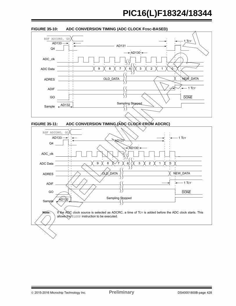
PIC16(L)F18324/18344
FIGURE 35-10: ADC CONVERSION TIMING (ADC CLOCK FOSC-BASED)
FIGURE 35-11: ADC CONVERSION TIMING (ADC CLOCK FROM ADCRC)
AD131
AD130
BSF ADCON0, GO
Q4
ADC_clk
ADC Data
ADRES
ADIF
GO
Sample
OLD_DATA
Sampling Stopped
DONE
NEW_DATA
9 8 7 3 2 1 0
1 TCY
6
AD133
1 TCY
AD132
AD132
AD131
AD130
BSF ADCON0, GO
Q4
ADC_clk
ADC Data
ADRES
ADIF
GO
Sample
OLD_DATA
Sampling Stopped
DONE
NEW_DATA
9 7 3 2 1 0
AD133
68
1 TCY
1 TCY
Note: If the ADC clock source is selected as ADCRC, a time of TCY is added before the ADC clock starts. Thisallows the SLEEP instruction to be executed.
2015-2016 Microchip Technology Inc. Preliminary DS40001800B-page 428
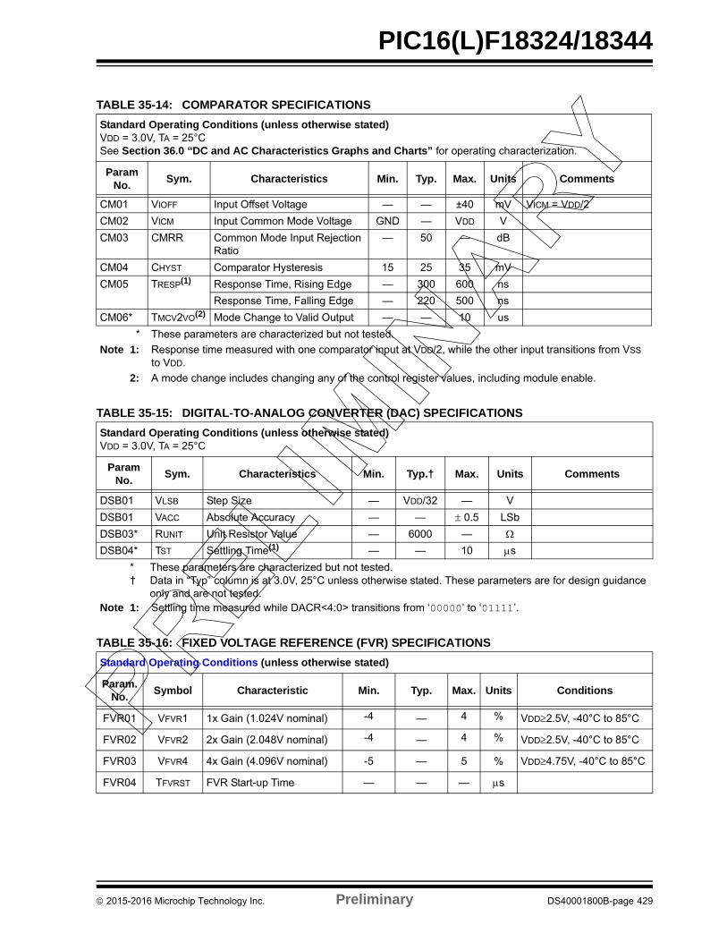
PIC16(L)F18324/18344
TABLE 35-14: COMPARATOR SPECIFICATIONS
Standard Operating Conditions (unless otherwise stated)VDD = 3.0V, TA = 25°CSee Section 36.0 “DC and AC Characteristics Graphs and Charts” for operating characterization.
ParamNo.
Sym. Characteristics Min. Typ. Max. Units Comments
CM01 VIOFF Input Offset Voltage — — ±40 mV VICM = VDD/2
CM02 VICM Input Common Mode Voltage GND — VDD V
CM03 CMRR Common Mode Input Rejection Ratio
— 50 — dB
CM04 CHYST Comparator Hysteresis 15 25 35 mV
CM05 TRESP(1) Response Time, Rising Edge — 300 600 ns
Response Time, Falling Edge — 220 500 ns
CM06* TMCV2VO(2) Mode Change to Valid Output — — 10 us
* These parameters are characterized but not tested.
Note 1: Response time measured with one comparator input at VDD/2, while the other input transitions from VSS to VDD.
2: A mode change includes changing any of the control register values, including module enable.
TABLE 35-15: DIGITAL-TO-ANALOG CONVERTER (DAC) SPECIFICATIONS
Standard Operating Conditions (unless otherwise stated)VDD = 3.0V, TA = 25°C
ParamNo.
Sym. Characteristics Min. Typ.† Max. Units Comments
DSB01 VLSB Step Size — VDD/32 — V
DSB01 VACC Absolute Accuracy — — 0.5 LSb
DSB03* RUNIT Unit Resistor Value — 6000 —
DSB04* TST Settling Time(1) — — 10 s
* These parameters are characterized but not tested.† Data in “Typ” column is at 3.0V, 25°C unless otherwise stated. These parameters are for design guidance
only and are not tested.Note 1: Settling time measured while DACR<4:0> transitions from ‘00000’ to ‘01111’.
TABLE 35-16: FIXED VOLTAGE REFERENCE (FVR) SPECIFICATIONS
Standard Operating Conditions (unless otherwise stated)
Param.No.
Symbol Characteristic Min. Typ. Max. Units Conditions
FVR01 VFVR1 1x Gain (1.024V nominal) -4 — 4 % VDD2.5V, -40°C to 85°C
FVR02 VFVR2 2x Gain (2.048V nominal) -4 — 4 % VDD2.5V, -40°C to 85°C
FVR03 VFVR4 4x Gain (4.096V nominal) -5 — 5 % VDD4.75V, -40°C to 85°C
FVR04 TFVRST FVR Start-up Time — — — s
2015-2016 Microchip Technology Inc. Preliminary DS40001800B-page 429
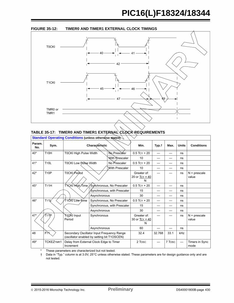
PIC16(L)F18324/18344
FIGURE 35-12: TIMER0 AND TIMER1 EXTERNAL CLOCK TIMINGS
TABLE 35-17: TIMER0 AND TIMER1 EXTERNAL CLOCK REQUIREMENTSStandard Operating Conditions (unless otherwise stated)
Param. No.
Sym. Characteristic Min. Typ.† Max. Units Conditions
40* TT0H T0CKI High Pulse Width No Prescaler 0.5 TCY + 20 — — ns
With Prescaler 10 — — ns
41* TT0L T0CKI Low Pulse Width No Prescaler 0.5 TCY + 20 — — ns
With Prescaler 10 — — ns
42* TT0P T0CKI Period Greater of:20 or TCY + 40
N
— — ns N = prescale value
45* TT1H T1CKI High Time Synchronous, No Prescaler 0.5 TCY + 20 — — ns
Synchronous, with Prescaler 15 — — ns
Asynchronous 30 — — ns
46* TT1L T1CKI Low Time Synchronous, No Prescaler 0.5 TCY + 20 — — ns
Synchronous, with Prescaler 15 — — ns
Asynchronous 30 — — ns
47* TT1P T1CKI Input Period
Synchronous Greater of:30 or TCY + 40
N
— — ns N = prescale value
Asynchronous 60 — — ns
48 FT1 Secondary Oscillator Input Frequency Range (oscillator enabled by setting bit T1OSCEN)
32.4 32.768 33.1 kHz
49* TCKEZTMR1 Delay from External Clock Edge to Timer Increment
2 TOSC — 7 TOSC — Timers in Sync mode
* These parameters are characterized but not tested.† Data in “Typ.” column is at 3.0V, 25°C unless otherwise stated. These parameters are for design guidance only and are
not tested.
T0CKI
T1CKI
40 41
42
45 46
47 49
TMR0 orTMR1
2015-2016 Microchip Technology Inc. Preliminary DS40001800B-page 430
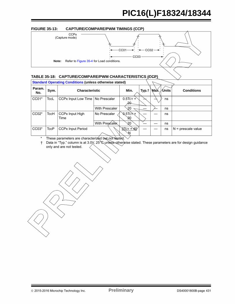
PIC16(L)F18324/18344
FIGURE 35-13: CAPTURE/COMPARE/PWM TIMINGS (CCP)
TABLE 35-18: CAPTURE/COMPARE/PWM CHARACTERISTICS (CCP)
Standard Operating Conditions (unless otherwise stated)
Param. No.
Sym. Characteristic Min. Typ.† Max. Units Conditions
CC01* TccL CCPx Input Low Time No Prescaler 0.5TCY + 20
— — ns
With Prescaler 20 — — ns
CC02* TccH CCPx Input High Time
No Prescaler 0.5TCY + 20
— — ns
With Prescaler 20 — — ns
CC03* TccP CCPx Input Period 3TCY + 40N
— — ns N = prescale value
* These parameters are characterized but not tested.† Data in “Typ.” column is at 3.0V, 25°C unless otherwise stated. These parameters are for design guidance
only and are not tested.
(Capture mode)
CC01 CC02
CC03
CCPx
Note: Refer to Figure 35-4 for Load conditions.
2015-2016 Microchip Technology Inc. Preliminary DS40001800B-page 431
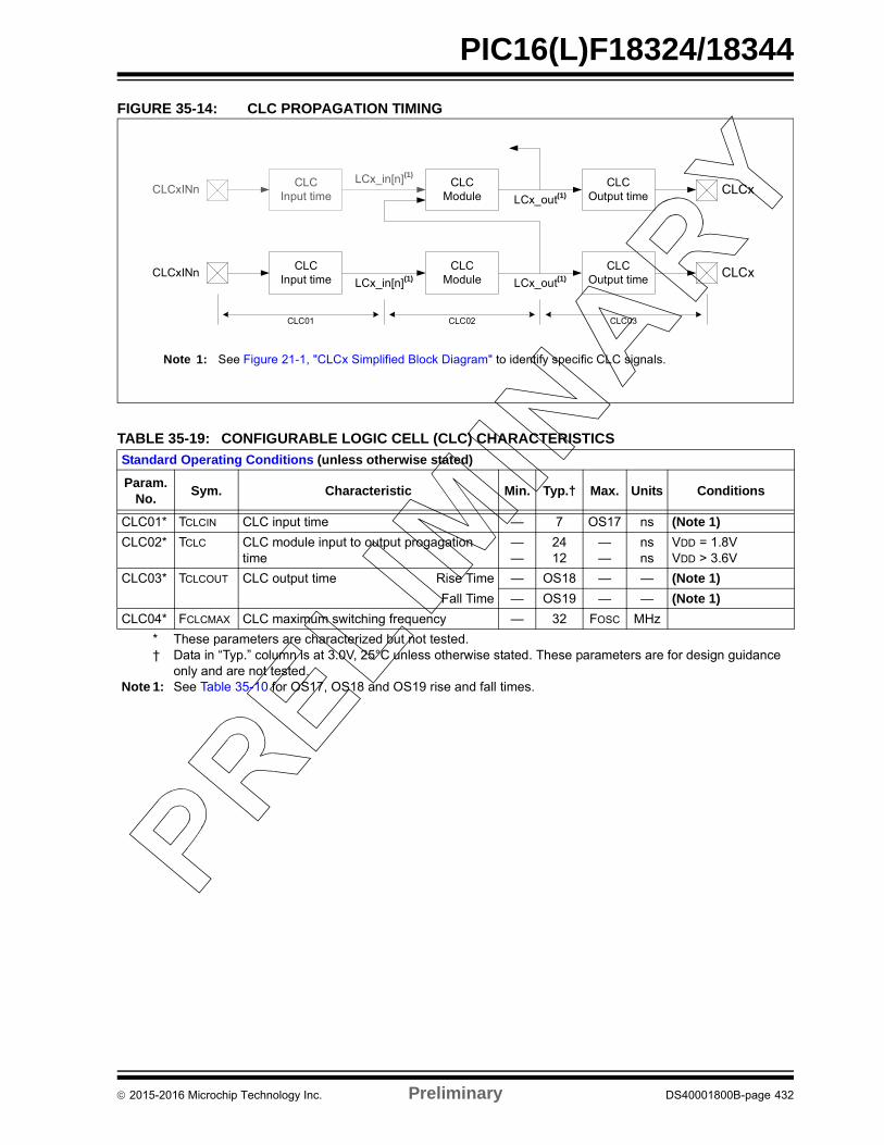
PIC16(L)F18324/18344
FIGURE 35-14: CLC PROPAGATION TIMING
LCx_in[n](1)
CLCOutput time
CLCInput time LCx_out(1)
CLCxCLCxINnCLC
Module
CLC01 CLC02 CLC03
LCx_in[n](1)CLC
Output timeCLC
Input time LCx_out(1)CLCxCLCxINn
CLCModule
Note 1: See Figure 21-1, "CLCx Simplified Block Diagram" to identify specific CLC signals.
TABLE 35-19: CONFIGURABLE LOGIC CELL (CLC) CHARACTERISTICS
Standard Operating Conditions (unless otherwise stated)
Param. No.
Sym. Characteristic Min. Typ.† Max. Units Conditions
CLC01* TCLCIN CLC input time — 7 OS17 ns (Note 1)
CLC02* TCLC CLC module input to output progagation time
——
2412
——
nsns
VDD = 1.8VVDD > 3.6V
CLC03* TCLCOUT CLC output time Rise Time — OS18 — — (Note 1)
Fall Time — OS19 — — (Note 1)
CLC04* FCLCMAX CLC maximum switching frequency — 32 FOSC MHz
* These parameters are characterized but not tested.† Data in “Typ.” column is at 3.0V, 25°C unless otherwise stated. These parameters are for design guidance
only and are not tested.Note 1: See Table 35-10 for OS17, OS18 and OS19 rise and fall times.
2015-2016 Microchip Technology Inc. Preliminary DS40001800B-page 432
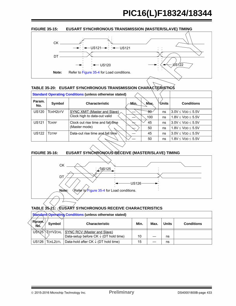
PIC16(L)F18324/18344
FIGURE 35-15: EUSART SYNCHRONOUS TRANSMISSION (MASTER/SLAVE) TIMING
FIGURE 35-16: EUSART SYNCHRONOUS RECEIVE (MASTER/SLAVE) TIMING
US121 US121
US120 US122
CK
DT
Note: Refer to Figure 35-4 for Load conditions.
TABLE 35-20: EUSART SYNCHRONOUS TRANSMISSION CHARACTERISTICS
Standard Operating Conditions (unless otherwise stated)
Param. No.
Symbol Characteristic Min. Max. Units Conditions
US120 TCKH2DTV SYNC XMIT (Master and Slave)Clock high to data-out valid
— 80 ns 3.0V VDD 5.5V
— 100 ns 1.8V VDD 5.5V
US121 TCKRF Clock out rise time and fall time (Master mode)
— 45 ns 3.0V VDD 5.5V
— 50 ns 1.8V VDD 5.5V
US122 TDTRF Data-out rise time and fall time — 45 ns 3.0V VDD 5.5V
— 50 ns 1.8V VDD 5.5V
US125
US126
CK
DT
Note: Refer to Figure 35-4 for Load conditions.
TABLE 35-21: EUSART SYNCHRONOUS RECEIVE CHARACTERISTICS
Standard Operating Conditions (unless otherwise stated)
Param. No.
Symbol Characteristic Min. Max. Units Conditions
US125 TDTV2CKL SYNC RCV (Master and Slave)Data-setup before CK (DT hold time) 10 — ns
US126 TCKL2DTL Data-hold after CK (DT hold time) 15 — ns
2015-2016 Microchip Technology Inc. Preliminary DS40001800B-page 433
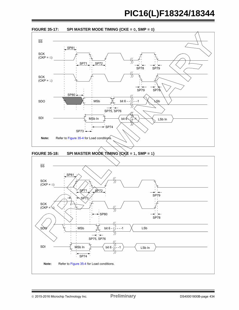
PIC16(L)F18324/18344
FIGURE 35-17: SPI MASTER MODE TIMING (CKE = 0, SMP = 0)
FIGURE 35-18: SPI MASTER MODE TIMING (CKE = 1, SMP = 1)
SS
SCK(CKP = 0)
SCK(CKP = 1)
SDO
SDI
SP81
SP71 SP72
SP73SP74
SP75, SP76
SP78SP79
SP80
SP79SP78
MSb LSbbit 6 - - - - - -1
MSb In LSb Inbit 6 - - - -1
Note: Refer to Figure 35-4 for Load conditions.
SS
SCK(CKP = 0)
SCK(CKP = 1)
SDO
SDI
SP81
SP71 SP72
SP74
SP75, SP76
SP78SP80
MSb
SP79SP73
MSb In
bit 6 - - - - - -1
LSb Inbit 6 - - - -1
LSb
Note: Refer to Figure 35-4 for Load conditions.
2015-2016 Microchip Technology Inc. Preliminary DS40001800B-page 434
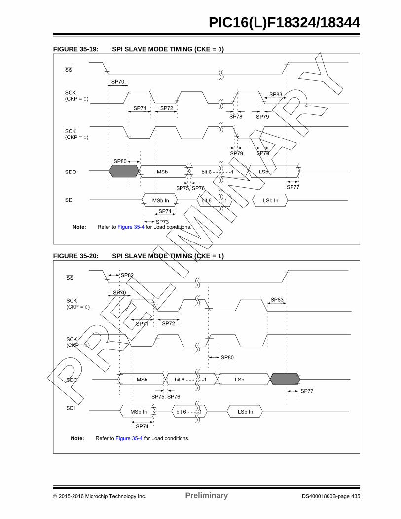
PIC16(L)F18324/18344
FIGURE 35-19: SPI SLAVE MODE TIMING (CKE = 0)
FIGURE 35-20: SPI SLAVE MODE TIMING (CKE = 1)
SS
SCK(CKP = 0)
SCK(CKP = 1)
SDO
SDI
SP70
SP71 SP72
SP73
SP74
SP75, SP76 SP77
SP78SP79
SP80
SP79SP78
MSb LSbbit 6 - - - - - -1
MSb In bit 6 - - - -1 LSb In
SP83
Note: Refer to Figure 35-4 for Load conditions.
SS
SCK(CKP = 0)
SCK(CKP = 1)
SDO
SDI
SP70
SP71 SP72
SP82
SP74
SP75, SP76
MSb bit 6 - - - - - -1 LSb
SP77
MSb In bit 6 - - - -1 LSb In
SP80
SP83
Note: Refer to Figure 35-4 for Load conditions.
2015-2016 Microchip Technology Inc. Preliminary DS40001800B-page 435
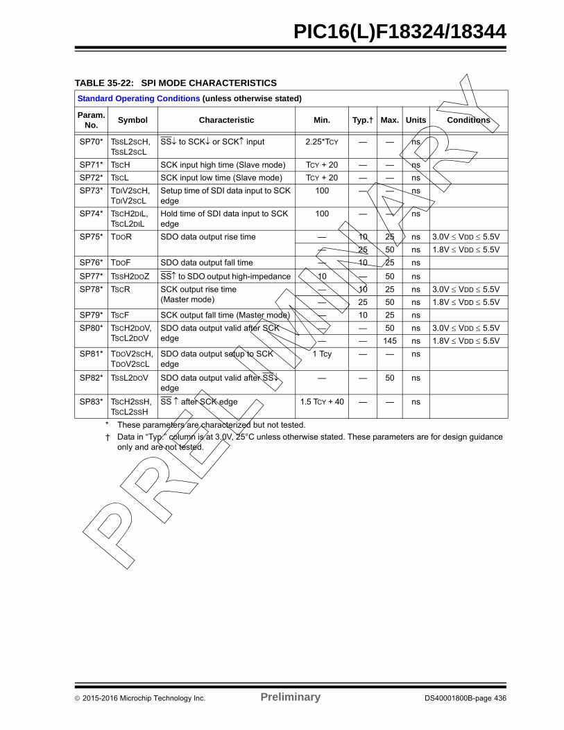
PIC16(L)F18324/18344
TABLE 35-22: SPI MODE CHARACTERISTICS
Standard Operating Conditions (unless otherwise stated)
Param. No.
Symbol Characteristic Min. Typ.† Max. Units Conditions
SP70* TSSL2SCH, TSSL2SCL
SS to SCK or SCK input 2.25*TCY — — ns
SP71* TSCH SCK input high time (Slave mode) TCY + 20 — — ns
SP72* TSCL SCK input low time (Slave mode) TCY + 20 — — ns
SP73* TDIV2SCH, TDIV2SCL
Setup time of SDI data input to SCK edge
100 — — ns
SP74* TSCH2DIL, TSCL2DIL
Hold time of SDI data input to SCK edge
100 — — ns
SP75* TDOR SDO data output rise time — 10 25 ns 3.0V VDD 5.5V
— 25 50 ns 1.8V VDD 5.5V
SP76* TDOF SDO data output fall time — 10 25 ns
SP77* TSSH2DOZ SS to SDO output high-impedance 10 — 50 ns
SP78* TSCR SCK output rise time (Master mode)
— 10 25 ns 3.0V VDD 5.5V
— 25 50 ns 1.8V VDD 5.5V
SP79* TSCF SCK output fall time (Master mode) — 10 25 ns
SP80* TSCH2DOV,TSCL2DOV
SDO data output valid after SCK edge
— — 50 ns 3.0V VDD 5.5V
— — 145 ns 1.8V VDD 5.5V
SP81* TDOV2SCH,TDOV2SCL
SDO data output setup to SCK edge
1 Tcy — — ns
SP82* TSSL2DOV SDO data output valid after SS edge
— — 50 ns
SP83* TSCH2SSH,TSCL2SSH
SS after SCK edge 1.5 TCY + 40 — — ns
* These parameters are characterized but not tested.
† Data in “Typ.” column is at 3.0V, 25°C unless otherwise stated. These parameters are for design guidance only and are not tested.
2015-2016 Microchip Technology Inc. Preliminary DS40001800B-page 436
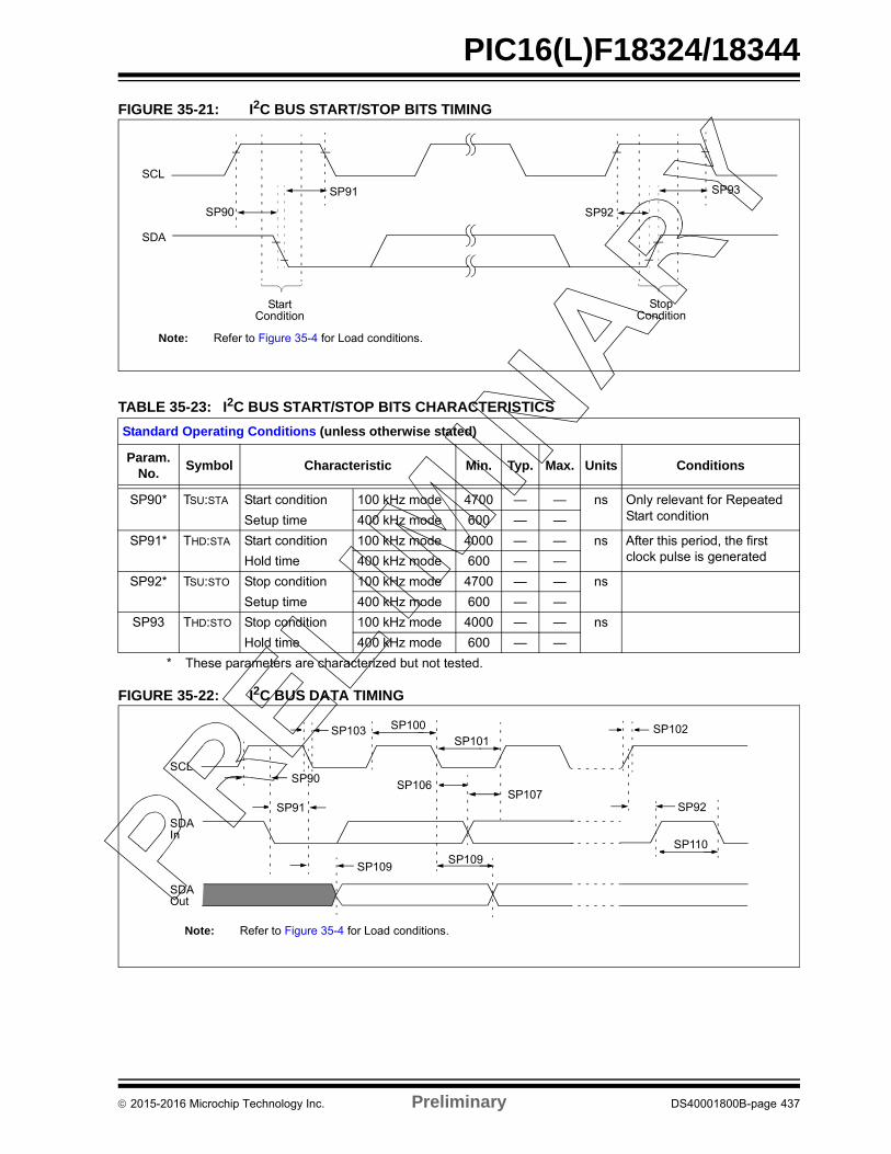
PIC16(L)F18324/18344
FIGURE 35-21: I2C BUS START/STOP BITS TIMING
FIGURE 35-22: I2C BUS DATA TIMING
SP91
SP92
SP93SCL
SDA
StartCondition
StopCondition
SP90
Note: Refer to Figure 35-4 for Load conditions.
TABLE 35-23: I2C BUS START/STOP BITS CHARACTERISTICS
Standard Operating Conditions (unless otherwise stated)
Param.No.
Symbol Characteristic Min. Typ. Max. Units Conditions
SP90* TSU:STA Start condition 100 kHz mode 4700 — — ns Only relevant for Repeated Start conditionSetup time 400 kHz mode 600 — —
SP91* THD:STA Start condition 100 kHz mode 4000 — — ns After this period, the first clock pulse is generatedHold time 400 kHz mode 600 — —
SP92* TSU:STO Stop condition 100 kHz mode 4700 — — ns
Setup time 400 kHz mode 600 — —
SP93 THD:STO Stop condition 100 kHz mode 4000 — — ns
Hold time 400 kHz mode 600 — —
* These parameters are characterized but not tested.
SP90
SP91 SP92
SP100SP101
SP103
SP106SP107
SP109SP109
SP110
SP102
SCL
SDAIn
SDAOut
Note: Refer to Figure 35-4 for Load conditions.
2015-2016 Microchip Technology Inc. Preliminary DS40001800B-page 437
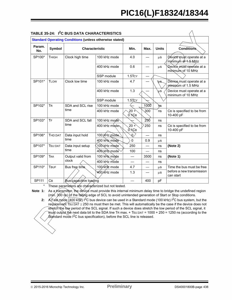
PIC16(L)F18324/18344
TABLE 35-24: I2C BUS DATA CHARACTERISTICS
Standard Operating Conditions (unless otherwise stated)
Param.No.
Symbol Characteristic Min. Max. Units Conditions
SP100* THIGH Clock high time 100 kHz mode 4.0 — s Device must operate at a minimum of 1.5 MHz
400 kHz mode 0.6 — s Device must operate at a minimum of 10 MHz
SSP module 1.5TCY —
SP101* TLOW Clock low time 100 kHz mode 4.7 — s Device must operate at a minimum of 1.5 MHz
400 kHz mode 1.3 — s Device must operate at a minimum of 10 MHz
SSP module 1.5TCY —
SP102* TR SDA and SCL rise time
100 kHz mode — 1000 ns
400 kHz mode 20 + 0.1CB
300 ns CB is specified to be from 10-400 pF
SP103* TF SDA and SCL fall time
100 kHz mode — 250 ns
400 kHz mode 20 + 0.1CB
250 ns CB is specified to be from 10-400 pF
SP106* THD:DAT Data input hold time
100 kHz mode 0 — ns
400 kHz mode 0 0.9 s
SP107* TSU:DAT Data input setup time
100 kHz mode 250 — ns (Note 2)
400 kHz mode 100 — ns
SP109* TAA Output valid from clock
100 kHz mode — 3500 ns (Note 1)
400 kHz mode — — ns
SP110* TBUF Bus free time 100 kHz mode 4.7 — s Time the bus must be free before a new transmission can start
400 kHz mode 1.3 — s
SP111 CB Bus capacitive loading — 400 pF
* These parameters are characterized but not tested.
Note 1: As a transmitter, the device must provide this internal minimum delay time to bridge the undefined region (min. 300 ns) of the falling edge of SCL to avoid unintended generation of Start or Stop conditions.
2: A Fast mode (400 kHz) I2C bus device can be used in a Standard mode (100 kHz) I2C bus system, but the requirement TSU:DAT 250 ns must then be met. This will automatically be the case if the device does not stretch the low period of the SCL signal. If such a device does stretch the low period of the SCL signal, it must output the next data bit to the SDA line TR max. + TSU:DAT = 1000 + 250 = 1250 ns (according to the Standard mode I2C bus specification), before the SCL line is released.
2015-2016 Microchip Technology Inc. Preliminary DS40001800B-page 438
2015-2016 Microchip Technology Inc. Preliminary DS40001800B-page 439
PIC16(L)F18324/18344
36.0 DC AND AC CHARACTERISTICS GRAPHS AND CHARTS
The graphs and tables provided in this section are for design guidance and are not tested.
In some graphs or tables, the data presented are outside specified operating range (i.e., outside specified VDD
range). This is for information only and devices are ensured to operate properly only within the specified range.
Unless otherwise noted, all graphs apply to both the L and LF devices.
“Typical” represents the mean of the distribution at 25C. “MAXIMUM”, “Max.”, “MINIMUM” or “Min.”represents (mean + 3) or (mean - 3) respectively, where is a standard deviation, over eachtemperature range.
Charts and graphs are not available at this time.
Note: The graphs and tables provided following this note are a statistical summary based on a limited number ofsamples and are provided for informational purposes only. The performance characteristics listed hereinare not tested or guaranteed. In some graphs or tables, the data presented may be outside the specifiedoperating range (e.g., outside specified power supply range) and therefore, outside the warranted range.
PIC16(L)F18324/18344
37.0 DEVELOPMENT SUPPORT
The PIC® microcontrollers (MCU) and dsPIC® digitalsignal controllers (DSC) are supported with a full rangeof software and hardware development tools:
• Integrated Development Environment- MPLAB® X IDE Software- MPLAB Xpress IDE Software- Microchip Code Configurator (MCC)
• Compilers/Assemblers/Linkers- MPLAB XC Compiler - MPASMTM Assembler- MPLINKTM Object Linker/
MPLIBTM Object Librarian- MPLAB Assembler/Linker/Librarian for
Various Device Families• Simulators
- MPLAB X SIM Software Simulator• Emulators
- MPLAB REAL ICE™ In-Circuit Emulator• In-Circuit Debuggers/Programmers
- MPLAB ICD 3- PICkit™ 3
• Device Programmers- MPLAB PM3 Device Programmer
• Low-Cost Demonstration/Development Boards, Evaluation Kits and Starter Kits
• Third-party development tools
37.1 MPLAB X Integrated Development Environment Software
The MPLAB X IDE is a single, unified graphical userinterface for Microchip and third-party software, andhardware development tool that runs on Windows®,Linux and Mac OS® X. Based on the NetBeans IDE,MPLAB X IDE is an entirely new IDE with a host of freesoftware components and plug-ins for high-performance application development and debugging.Moving between tools and upgrading from softwaresimulators to hardware debugging and programmingtools is simple with the seamless user interface.
With complete project management, visual call graphs,a configurable watch window and a feature-rich editorthat includes code completion and context menus,MPLAB X IDE is flexible and friendly enough for newusers. With the ability to support multiple tools onmultiple projects with simultaneous debugging, MPLABX IDE is also suitable for the needs of experiencedusers.
Feature-Rich Editor:
• Color syntax highlighting• Smart code completion makes suggestions and
provides hints as you type• Automatic code formatting based on user-defined
rules• Live parsing
User-Friendly, Customizable Interface:
• Fully customizable interface: toolbars, toolbar buttons, windows, window placement, etc.
• Call graph window
Project-Based Workspaces:
• Multiple projects• Multiple tools• Multiple configurations• Simultaneous debugging sessions
File History and Bug Tracking:
• Local file history feature• Built-in support for Bugzilla issue tracker
2015-2016 Microchip Technology Inc. Preliminary DS40001800B-page 440
PIC16(L)F18324/18344
37.2 MPLAB XC Compilers
The MPLAB XC Compilers are complete ANSI Ccompilers for all of Microchip’s 8, 16, and 32-bit MCUand DSC devices. These compilers provide powerfulintegration capabilities, superior code optimization andease of use. MPLAB XC Compilers run on Windows,Linux or MAC OS X.
For easy source level debugging, the compilers providedebug information that is optimized to the MPLAB XIDE.
The free MPLAB XC Compiler editions support alldevices and commands, with no time or memoryrestrictions, and offer sufficient code optimization formost applications.
MPLAB XC Compilers include an assembler, linker andutilities. The assembler generates relocatable objectfiles that can then be archived or linked with other relo-catable object files and archives to create an execut-able file. MPLAB XC Compiler uses the assembler toproduce its object file. Notable features of the assem-bler include:
• Support for the entire device instruction set• Support for fixed-point and floating-point data• Command-line interface• Rich directive set• Flexible macro language• MPLAB X IDE compatibility
37.3 MPASM Assembler
The MPASM Assembler is a full-featured, universalmacro assembler for PIC10/12/16/18 MCUs.
The MPASM Assembler generates relocatable objectfiles for the MPLINK Object Linker, Intel® standard HEXfiles, MAP files to detail memory usage and symbolreference, absolute LST files that contain source linesand generated machine code, and COFF files fordebugging.
The MPASM Assembler features include:
• Integration into MPLAB X IDE projects• User-defined macros to streamline
assembly code• Conditional assembly for multipurpose
source files• Directives that allow complete control over the
assembly process
37.4 MPLINK Object Linker/MPLIB Object Librarian
The MPLINK Object Linker combines relocatableobjects created by the MPASM Assembler. It can linkrelocatable objects from precompiled libraries, usingdirectives from a linker script.
The MPLIB Object Librarian manages the creation andmodification of library files of precompiled code. Whena routine from a library is called from a source file, onlythe modules that contain that routine will be linked inwith the application. This allows large libraries to beused efficiently in many different applications.
The object linker/library features include:
• Efficient linking of single libraries instead of many smaller files
• Enhanced code maintainability by grouping related modules together
• Flexible creation of libraries with easy module listing, replacement, deletion and extraction
37.5 MPLAB Assembler, Linker and Librarian for Various Device Families
MPLAB Assembler produces relocatable machinecode from symbolic assembly language for PIC24,PIC32 and dsPIC DSC devices. MPLAB XC Compileruses the assembler to produce its object file. Theassembler generates relocatable object files that canthen be archived or linked with other relocatable objectfiles and archives to create an executable file. Notablefeatures of the assembler include:
• Support for the entire device instruction set• Support for fixed-point and floating-point data• Command-line interface• Rich directive set• Flexible macro language• MPLAB X IDE compatibility
2015-2016 Microchip Technology Inc. Preliminary DS40001800B-page 441
PIC16(L)F18324/18344
37.6 MPLAB X SIM Software Simulator
The MPLAB X SIM Software Simulator allows codedevelopment in a PC-hosted environment by simulat-ing the PIC MCUs and dsPIC DSCs on an instructionlevel. On any given instruction, the data areas can beexamined or modified and stimuli can be applied froma comprehensive stimulus controller. Registers can belogged to files for further run-time analysis. The tracebuffer and logic analyzer display extend the power ofthe simulator to record and track program execution,actions on I/O, most peripherals and internal registers.
The MPLAB X SIM Software Simulator fully supportssymbolic debugging using the MPLAB XC Compilers,and the MPASM and MPLAB Assemblers. The soft-ware simulator offers the flexibility to develop anddebug code outside of the hardware laboratory envi-ronment, making it an excellent, economical softwaredevelopment tool.
37.7 MPLAB REAL ICE In-Circuit Emulator System
The MPLAB REAL ICE In-Circuit Emulator System isMicrochip’s next generation high-speed emulator forMicrochip Flash DSC and MCU devices. It debugs andprograms all 8, 16 and 32-bit MCU, and DSC deviceswith the easy-to-use, powerful graphical user interface ofthe MPLAB X IDE.
The emulator is connected to the design engineer’sPC using a high-speed USB 2.0 interface and isconnected to the target with either a connectorcompatible with in-circuit debugger systems (RJ-11)or with the new high-speed, noise tolerant, Low-Voltage Differential Signal (LVDS) interconnection(CAT5).
The emulator is field upgradeable through futurefirmware downloads in MPLAB X IDE. MPLAB REALICE offers significant advantages over competitiveemulators including full-speed emulation, run-timevariable watches, trace analysis, complex breakpoints,logic probes, a ruggedized probe interface and long (upto three meters) interconnection cables.
37.8 MPLAB ICD 3 In-Circuit Debugger System
The MPLAB ICD 3 In-Circuit Debugger System isMicrochip’s most cost-effective, high-speed hardwaredebugger/programmer for Microchip Flash DSC andMCU devices. It debugs and programs PIC Flashmicrocontrollers and dsPIC DSCs with the powerful,yet easy-to-use graphical user interface of the MPLABIDE.
The MPLAB ICD 3 In-Circuit Debugger probe isconnected to the design engineer’s PC using a high-speed USB 2.0 interface and is connected to the targetwith a connector compatible with the MPLAB ICD 2 orMPLAB REAL ICE systems (RJ-11). MPLAB ICD 3supports all MPLAB ICD 2 headers.
37.9 PICkit 3 In-Circuit Debugger/Programmer
The MPLAB PICkit 3 allows debugging andprogramming of PIC and dsPIC Flash microcontrollersat a most affordable price point using the powerfulgraphical user interface of the MPLAB IDE. TheMPLAB PICkit 3 is connected to the design engineer’sPC using a full-speed USB interface and can beconnected to the target via a Microchip debug (RJ-11)connector (compatible with MPLAB ICD 3 and MPLABREAL ICE). The connector uses two device I/O pinsand the Reset line to implement in-circuit debuggingand In-Circuit Serial Programming™ (ICSP™).
37.10 MPLAB PM3 Device Programmer
The MPLAB PM3 Device Programmer is a universal,CE compliant device programmer with programmablevoltage verification at VDDMIN and VDDMAX formaximum reliability. It features a large LCD display(128 x 64) for menus and error messages, and a mod-ular, detachable socket assembly to support variouspackage types. The ICSP cable assembly is includedas a standard item. In Stand-Alone mode, the MPLABPM3 Device Programmer can read, verify and programPIC devices without a PC connection. It can also setcode protection in this mode. The MPLAB PM3connects to the host PC via an RS-232 or USB cable.The MPLAB PM3 has high-speed communications andoptimized algorithms for quick programming of largememory devices, and incorporates an MMC card for filestorage and data applications.
2015-2016 Microchip Technology Inc. Preliminary DS40001800B-page 442
PIC16(L)F18324/18344
37.11 Demonstration/Development Boards, Evaluation Kits, and Starter Kits
A wide variety of demonstration, development andevaluation boards for various PIC MCUs and dsPICDSCs allows quick application development on fullyfunctional systems. Most boards include prototypingareas for adding custom circuitry and provide applica-tion firmware and source code for examination andmodification.
The boards support a variety of features, including LEDs,temperature sensors, switches, speakers, RS-232interfaces, LCD displays, potentiometers and additionalEEPROM memory.
The demonstration and development boards can beused in teaching environments, for prototyping customcircuits and for learning about various microcontrollerapplications.
In addition to the PICDEM™ and dsPICDEM™demonstration/development board series of circuits,Microchip has a line of evaluation kits anddemonstration software for analog filter design,KEELOQ® security ICs, CAN, IrDA®, PowerSmartbattery management, SEEVAL® evaluation system,Sigma-Delta ADC, flow rate sensing, plus many more.
Also available are starter kits that contain everythingneeded to experience the specified device. This usuallyincludes a single application and debug capability, allon one board.
Check the Microchip web page (www.microchip.com)for the complete list of demonstration, developmentand evaluation kits.
37.12 Third-Party Development Tools
Microchip also offers a great collection of tools fromthird-party vendors. These tools are carefully selectedto offer good value and unique functionality.
• Device Programmers and Gang Programmers from companies, such as SoftLog and CCS
• Software Tools from companies, such as Gimpel and Trace Systems
• Protocol Analyzers from companies, such as Saleae and Total Phase
• Demonstration Boards from companies, such as MikroElektronika, Digilent® and Olimex
• Embedded Ethernet Solutions from companies, such as EZ Web Lynx, WIZnet and IPLogika®
2015-2016 Microchip Technology Inc. Preliminary DS40001800B-page 443
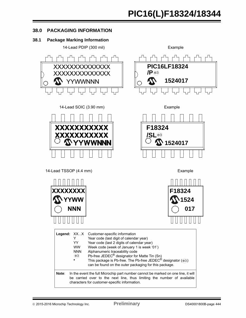
PIC16(L)F18324/18344
38.0 PACKAGING INFORMATION
38.1 Package Marking Information
Legend: XX...X Customer-specific informationY Year code (last digit of calendar year)YY Year code (last 2 digits of calendar year)WW Week code (week of January 1 is week ‘01’)NNN Alphanumeric traceability code Pb-free JEDEC® designator for Matte Tin (Sn)* This package is Pb-free. The Pb-free JEDEC® designator ( )
can be found on the outer packaging for this package.
Note: In the event the full Microchip part number cannot be marked on one line, it willbe carried over to the next line, thus limiting the number of availablecharacters for customer-specific information.
3e
3e
28-Lead SOIC (7.50 mm) Example
14-Lead PDIP (300 mil) Example
14-Lead SOIC (3.90 mm) Example
1524017
3e
PIC16LF18324/P
F18324/SL
1524017
3e
14-Lead TSSOP (4.4 mm) Example
YYWWNNN
XXXXXXXX F18324
1524
017
2015-2016 Microchip Technology Inc. Preliminary DS40001800B-page 444
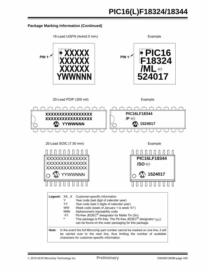
PIC16(L)F18324/18344
Package Marking Information (Continued)
20-Lead PDIP (300 mil) Example
XXXXXXXXXXXXXXXXXXXXXXXXXXXXXXXXXX
YYWWNNN
16-Lead UQFN (4x4x0.5 mm) Example
PIN 1 PIN 1 PIC16F18324
5240173e/ML
20-Lead SOIC (7.50 mm) Example
Legend: XX...X Customer-specific informationY Year code (last digit of calendar year)YY Year code (last 2 digits of calendar year)WW Week code (week of January 1 is week ‘01’)NNN Alphanumeric traceability code Pb-free JEDEC® designator for Matte Tin (Sn)* This package is Pb-free. The Pb-free JEDEC® designator ( )
can be found on the outer packaging for this package.
Note: In the event the full Microchip part number cannot be marked on one line, it willbe carried over to the next line, thus limiting the number of availablecharacters for customer-specific information.
3e
3e
PIC16LF18344/SO
1524017
PIC16LF18344/P
15240173e
3e
2015-2016 Microchip Technology Inc. Preliminary DS40001800B-page 445
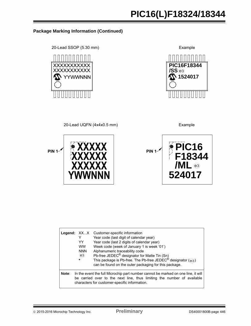
PIC16(L)F18324/18344
Package Marking Information (Continued)
20-Lead UQFN (4x4x0.5 mm) Example
PIN 1 PIN 1
Legend: XX...X Customer-specific informationY Year code (last digit of calendar year)YY Year code (last 2 digits of calendar year)WW Week code (week of January 1 is week ‘01’)NNN Alphanumeric traceability code Pb-free JEDEC® designator for Matte Tin (Sn)* This package is Pb-free. The Pb-free JEDEC® designator ( )
can be found on the outer packaging for this package.
Note: In the event the full Microchip part number cannot be marked on one line, it willbe carried over to the next line, thus limiting the number of availablecharacters for customer-specific information.
3e
3e
PIC16F18344/ML
524017
20-Lead SSOP (5.30 mm) Example
PIC16F18344/SS
15240173e
3e
2015-2016 Microchip Technology Inc. Preliminary DS40001800B-page 446
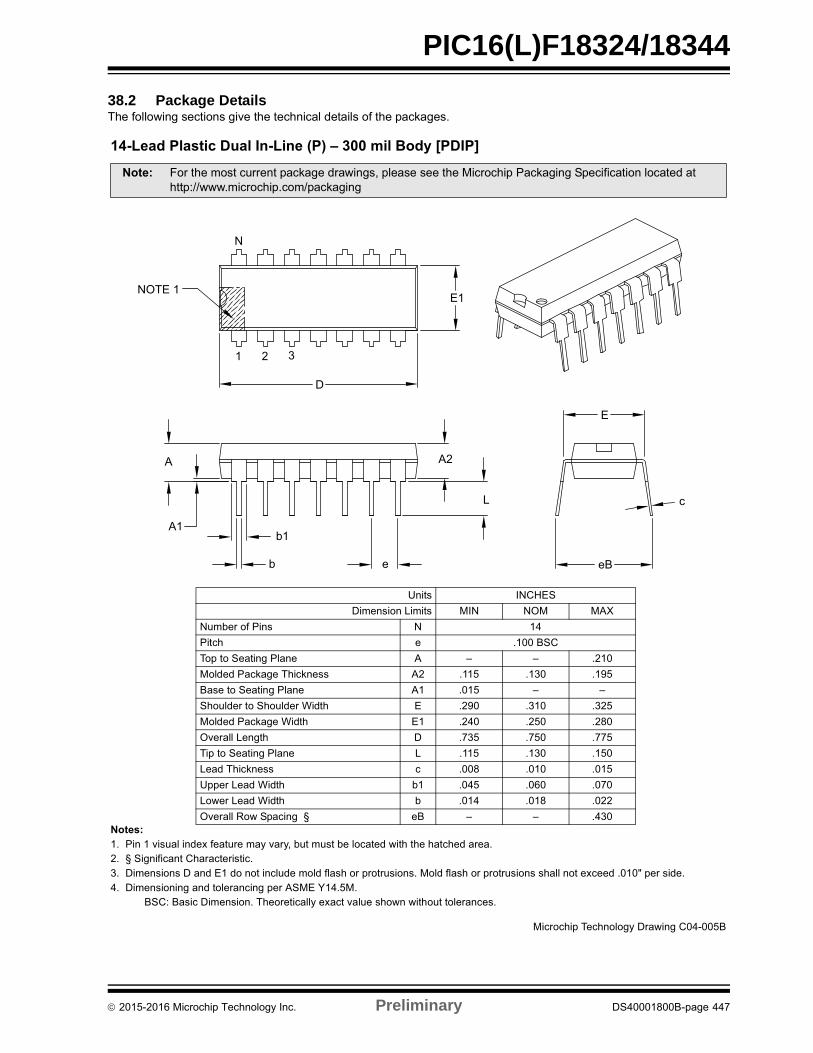
PIC16(L)F18324/18344
38.2 Package DetailsThe following sections give the technical details of the packages.
! !"#$%&"'*;"&'"!&;&#?&&&# @%&G&!&J '!!#X#&"#'#%!&"!!#%!&"!!!&$#Y!# '!#&X[\
]G^]!'! &$&"!??&"&&!
! `&'!&"&j#?!*!!&j%&&#&&&^???''j
|&! G~X'!'&!
"';%! & ]G && ##j j!! \ J \]!&& \ "#&"##& X J J\##j#& X \ & J\ \ \ && \ J \# j!! \|##& ; \ ?##& ; ?@ ] J
N
E1
D
NOTE 1
1 2 3
E
c
eB
A2
L
A
A1b1
b e
? G\]
2015-2016 Microchip Technology Inc. Preliminary DS40001800B-page 447
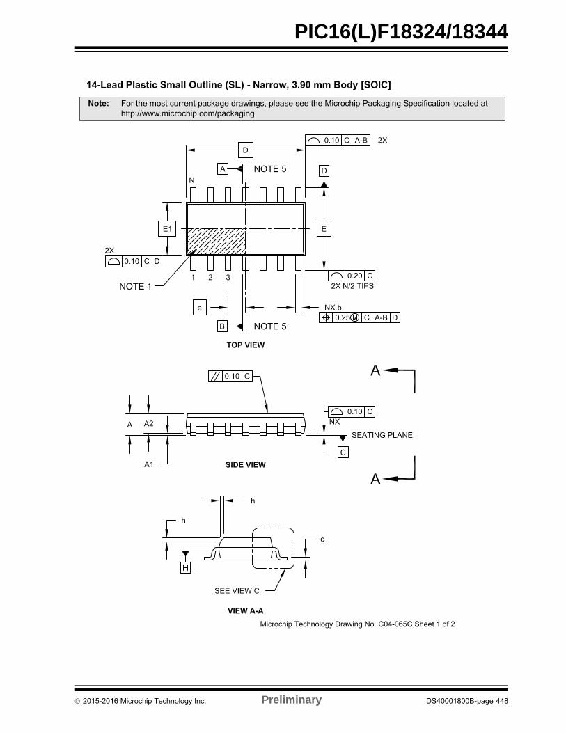
PIC16(L)F18324/18344
Note: For the most current package drawings, please see the Microchip Packaging Specification located at http://www.microchip.com/packaging
2015-2016 Microchip Technology Inc. Preliminary DS40001800B-page 448
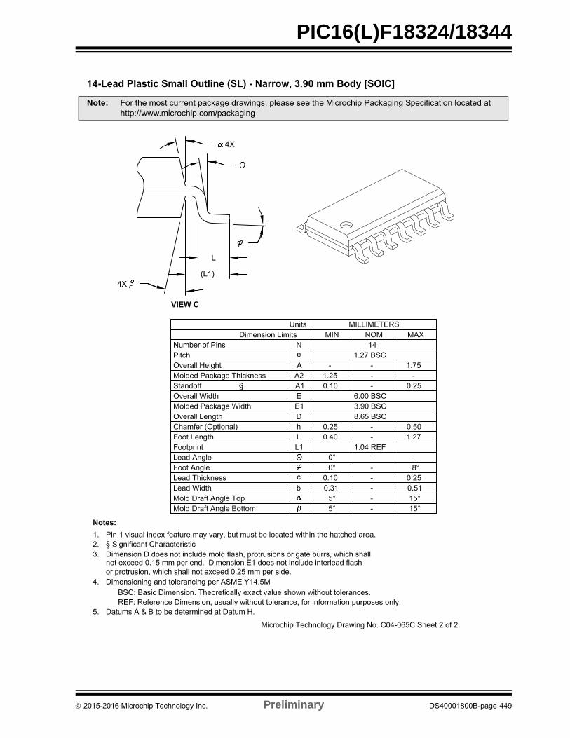
PIC16(L)F18324/18344
Note: For the most current package drawings, please see the Microchip Packaging Specification located at http://www.microchip.com/packaging
2015-2016 Microchip Technology Inc. Preliminary DS40001800B-page 449
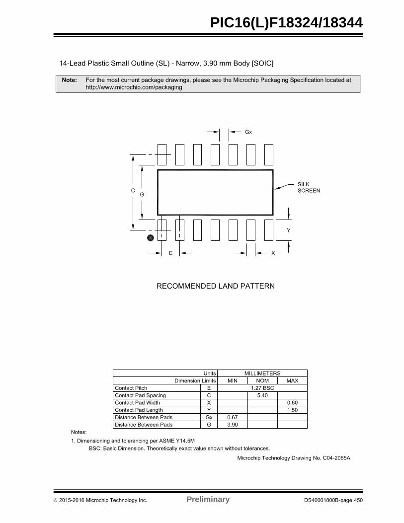
PIC16(L)F18324/18344
! `&'!&"&j#?!*!!&j%&&#&&&^???''j
2015-2016 Microchip Technology Inc. Preliminary DS40001800B-page 450
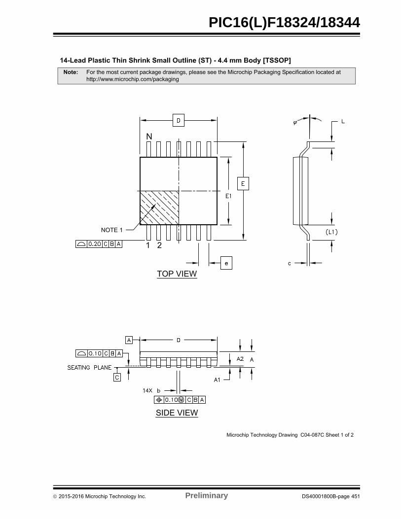
PIC16(L)F18324/18344
Note: For the most current package drawings, please see the Microchip Packaging Specification located at http://www.microchip.com/packaging
2015-2016 Microchip Technology Inc. Preliminary DS40001800B-page 451
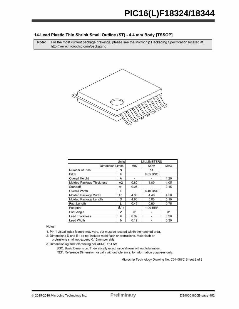
PIC16(L)F18324/18344
Note: For the most current package drawings, please see the Microchip Packaging Specification located at http://www.microchip.com/packaging
2015-2016 Microchip Technology Inc. Preliminary DS40001800B-page 452
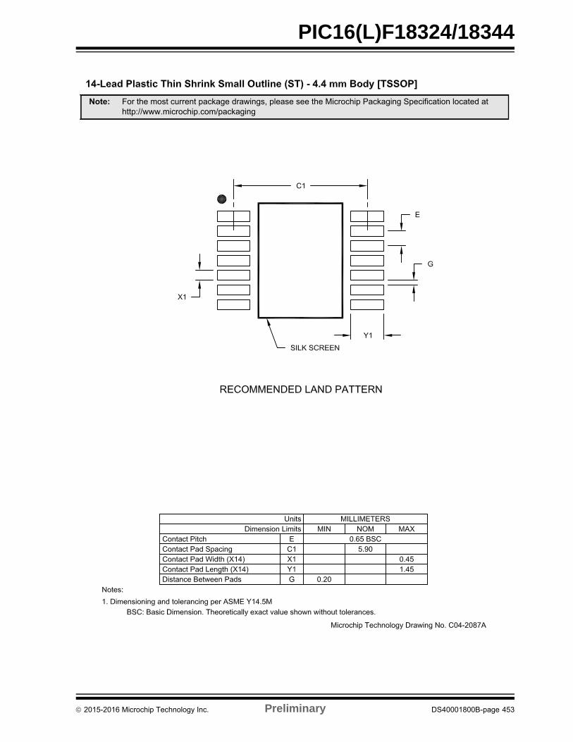
PIC16(L)F18324/18344
Note: For the most current package drawings, please see the Microchip Packaging Specification located at http://www.microchip.com/packaging
2015-2016 Microchip Technology Inc. Preliminary DS40001800B-page 453
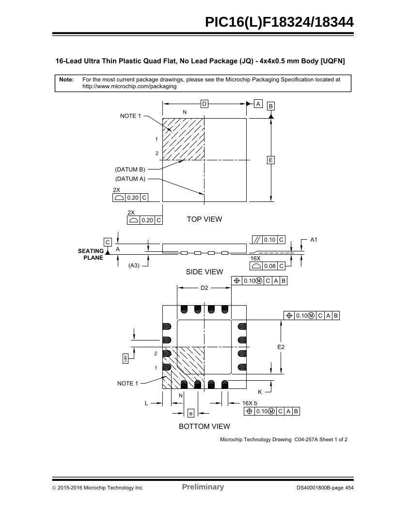
PIC16(L)F18324/18344
BA
0.20 C
0.20 C
0.10 C A B
(DATUM B)(DATUM A)
CSEATING
PLANE
NOTE 1
1
2
N
2XTOP VIEW
SIDE VIEW
BOTTOM VIEW
For the most current package drawings, please see the Microchip Packaging Specification located athttp://www.microchip.com/packaging
Note:
NOTE 1
1
2
N
0.10 C A B
0.10 C A B
0.10 C
0.08 C
A1
Microchip Technology Drawing C04-257A Sheet 1 of 2
16-Lead Ultra Thin Plastic Quad Flat, No Lead Package (JQ) - 4x4x0.5 mm Body [UQFN]
D
E
A
(A3)
16X b
e
e2
2X
D2
E2
K
L
16X
2015-2016 Microchip Technology Inc. Preliminary DS40001800B-page 454
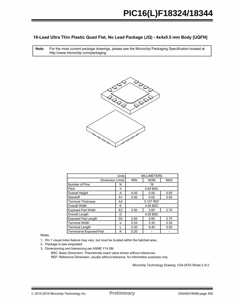
PIC16(L)F18324/18344
Microchip Technology Drawing C04-257A Sheet 2 of 2
For the most current package drawings, please see the Microchip Packaging Specification located athttp://www.microchip.com/packaging
Note:
Number of Pins
Overall Height
Terminal Width
Overall Width
Overall Length
Terminal Length
Exposed Pad Width
Exposed Pad Length
Terminal Thickness
Pitch
Standoff
UnitsDimension Limits
A1A
b
DE2
D2
A3
e
L
E
N0.65 BSC
0.127 REF
2.50
2.50
0.300.25
0.450.00
0.30
4.00 BSC
0.40
2.60
2.60
0.500.02
4.00 BSC
MILLIMETERSMIN NOM
16
2.70
2.70
0.500.35
0.550.05
MAX
K -0.20 -
REF: Reference Dimension, usually without tolerance, for information purposes only.BSC: Basic Dimension. Theoretically exact value shown without tolerances.
1.2.3.
Notes:
Pin 1 visual index feature may vary, but must be located within the hatched area.Package is saw singulatedDimensioning and tolerancing per ASME Y14.5M
Terminal-to-Exposed-Pad
16-Lead Ultra Thin Plastic Quad Flat, No Lead Package (JQ) - 4x4x0.5 mm Body [UQFN]
2015-2016 Microchip Technology Inc. Preliminary DS40001800B-page 455
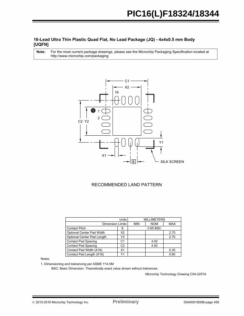
PIC16(L)F18324/18344
RECOMMENDED LAND PATTERN
For the most current package drawings, please see the Microchip Packaging Specification located athttp://www.microchip.com/packaging
Note:
SILK SCREEN
Dimension LimitsUnits
C2
Optional Center Pad Width
Contact Pad Spacing
Optional Center Pad Length
Contact Pitch
Y2X2
2.702.70
MILLIMETERS
0.65 BSCMIN
EMAX
4.00
Contact Pad Length (X16)Contact Pad Width (X16)
Y1X1
0.800.35
BSC: Basic Dimension. Theoretically exact value shown without tolerances.
Notes:1. Dimensioning and tolerancing per ASME Y14.5M
Microchip Technology Drawing C04-2257A
NOM
16-Lead Ultra Thin Plastic Quad Flat, No Lead Package (JQ) - 4x4x0.5 mm Body
C2
C1
X2
Y2
X1
E
Y1
C1 4.00Contact Pad Spacing
1
2
16
[UQFN]
2015-2016 Microchip Technology Inc. Preliminary DS40001800B-page 456
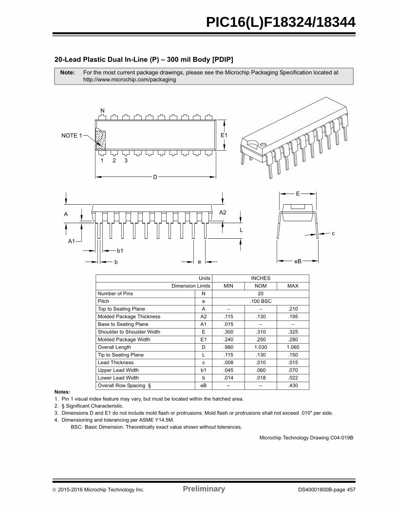
PIC16(L)F18324/18344
"
! !"#$%&"'*;"&'"!&;&#?&&&# @%&G&!&J '!!#X#&"#'#%!&"!!#%!&"!!!&$#Y!# '!#&X[\
]G^ ]!'! &$&"!??&"&&!
! `&'!&"&j#?!*!!&j%&&#&&&^???''j
|&! G~X'!'&!
"';%! & ]G && ##j j!! \ J \]!&& \ "#&"##& X J J J\##j#& X \ & J && \ J \# j!! \|##& ; \ ?##& ; ?@ ] J
N
E1NOTE 1
D
1 2 3
A
A1
A2
L
e
b1
b
E
c
eB
? G]
2015-2016 Microchip Technology Inc. Preliminary DS40001800B-page 457
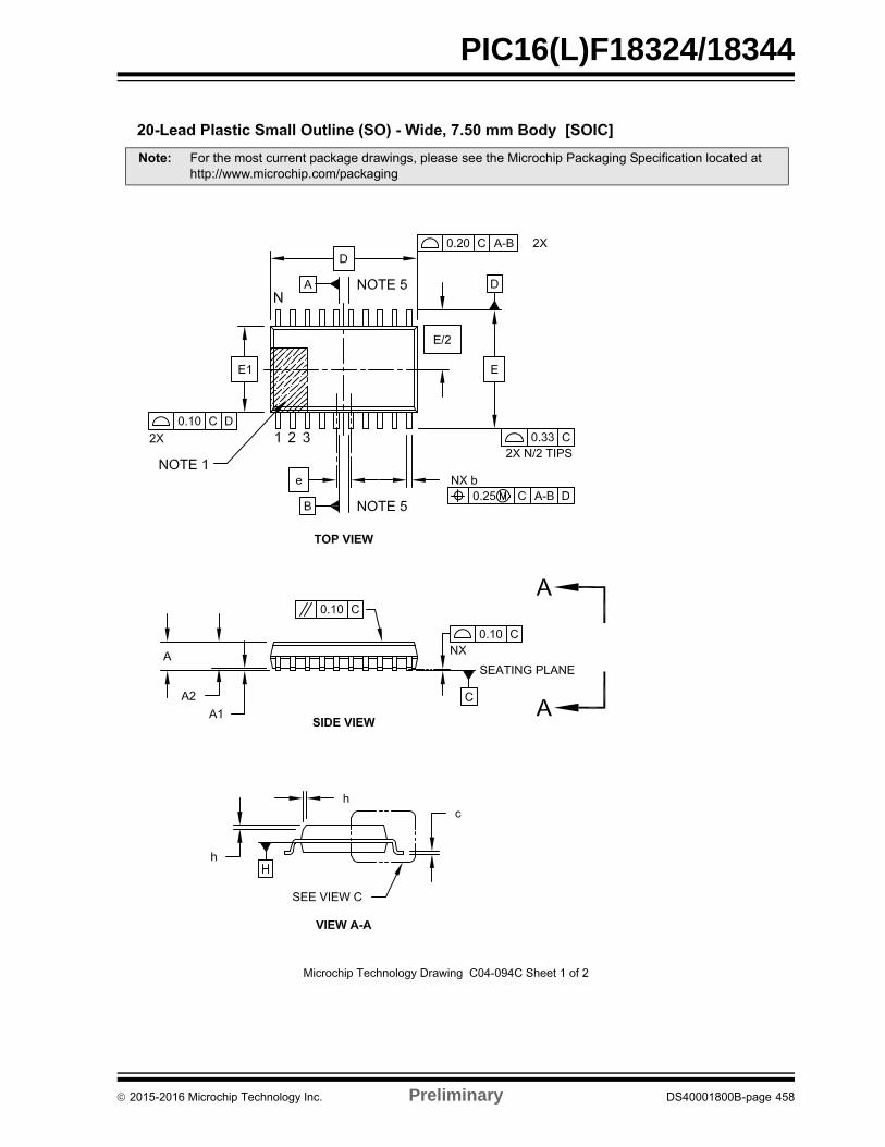
PIC16(L)F18324/18344
Note: For the most current package drawings, please see the Microchip Packaging Specification located at http://www.microchip.com/packaging
2015-2016 Microchip Technology Inc. Preliminary DS40001800B-page 458
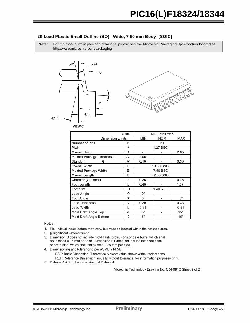
PIC16(L)F18324/18344
Note: For the most current package drawings, please see the Microchip Packaging Specification located at http://www.microchip.com/packaging
2015-2016 Microchip Technology Inc. Preliminary DS40001800B-page 459

PIC16(L)F18324/18344
Note: For the most current package drawings, please see the Microchip Packaging Specification located at http://www.microchip.com/packaging
2015-2016 Microchip Technology Inc. Preliminary DS40001800B-page 460
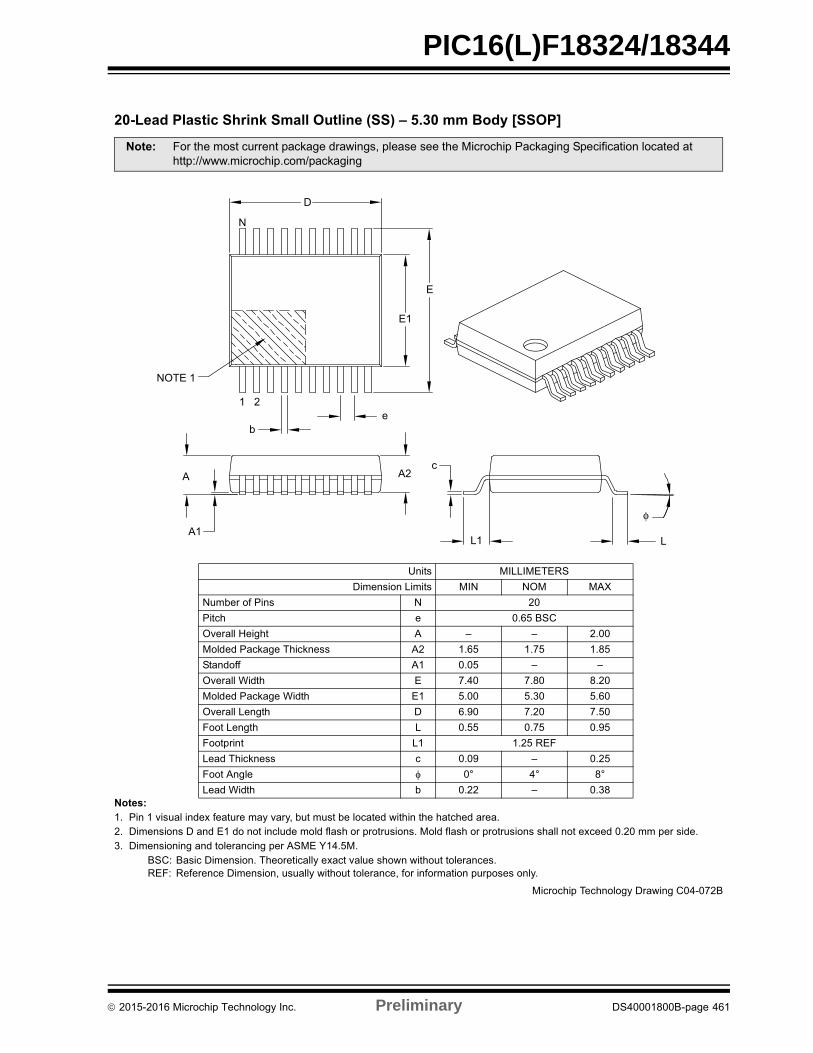
PIC16(L)F18324/18344
" #$%&#' ##*+##'
! !"#$%&"'*;"&'"!&;&#?&&&# '!!#X#&"#'#%!&"!!#%!&"!!!&$#''!#J '!#&X[\
]G^ ]!'! &$&"!??&"&&!X`^ %'!*"!"?&"&&*%%'&"!!
! `&'!&"&j#?!*!!&j%&&#&&&^???''j
|&! X X'!'&!
"';%! & \]G~& ##j j!! \ \ \&#%% \ #& X ##j#& X \ \J \& \`&& \\ \ \`&& \X`# j!! \`& ##& ; J
φ
LL1
A2c
eb
A1
A
1 2
NOTE 1
E1
E
D
N
? G]
2015-2016 Microchip Technology Inc. Preliminary DS40001800B-page 461
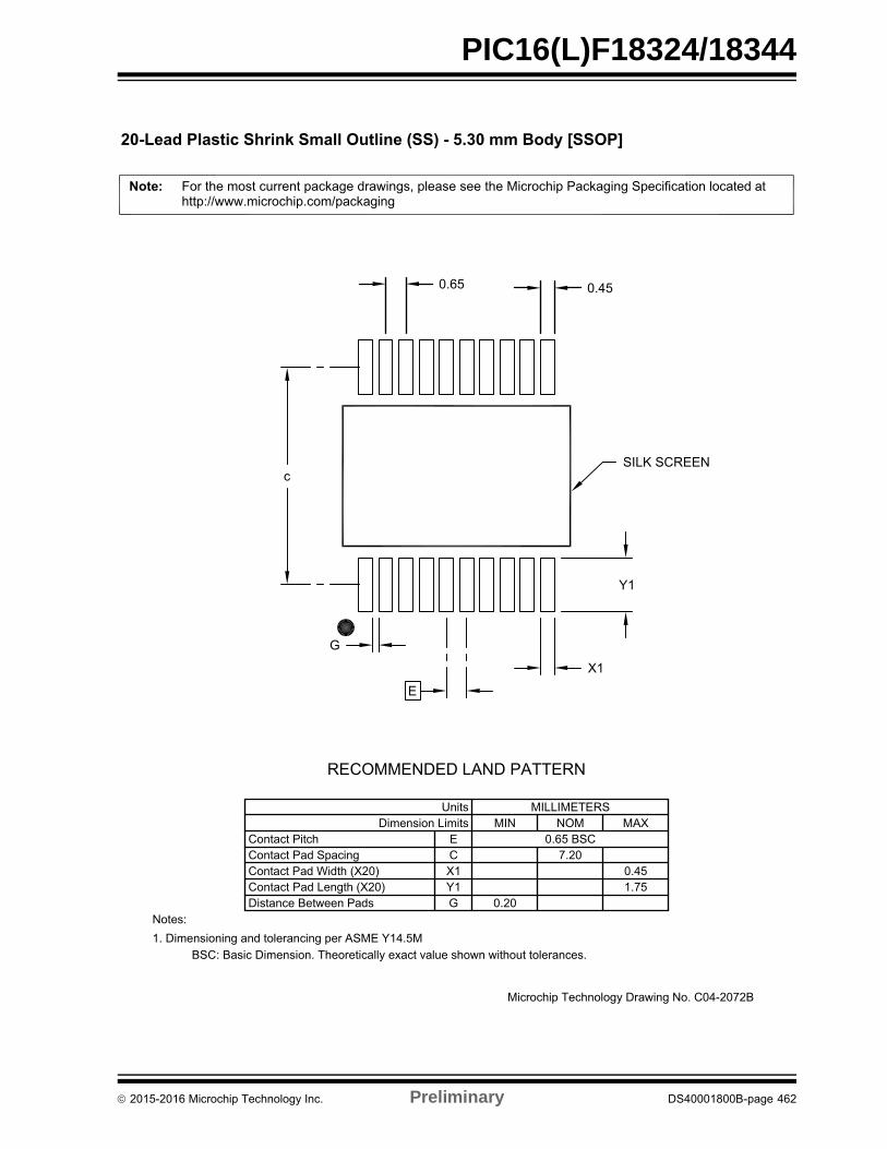
PIC16(L)F18324/18344
RECOMMENDED LAND PATTERN
Microchip Technology Drawing No. C04-2072B
20-Lead Plastic Shrink Small Outline (SS) - 5.30 mm Body [SSOP]
For the most current package drawings, please see the Microchip Packaging Specification located athttp://www.microchip.com/packaging
Note:
c
G
E
X1
Y1
SILK SCREEN
Dimension LimitsUnits
CContact Pad SpacingContact Pitch
MILLIMETERS
0.65 BSCMIN
EMAX
7.20
Contact Pad Length (X20)Contact Pad Width (X20)
Y1X1
1.750.45
BSC: Basic Dimension. Theoretically exact value shown without tolerances.
Notes:1. Dimensioning and tolerancing per ASME Y14.5M
GDistance Between Pads 0.20
NOM
0.450.65
2015-2016 Microchip Technology Inc. Preliminary DS40001800B-page 462
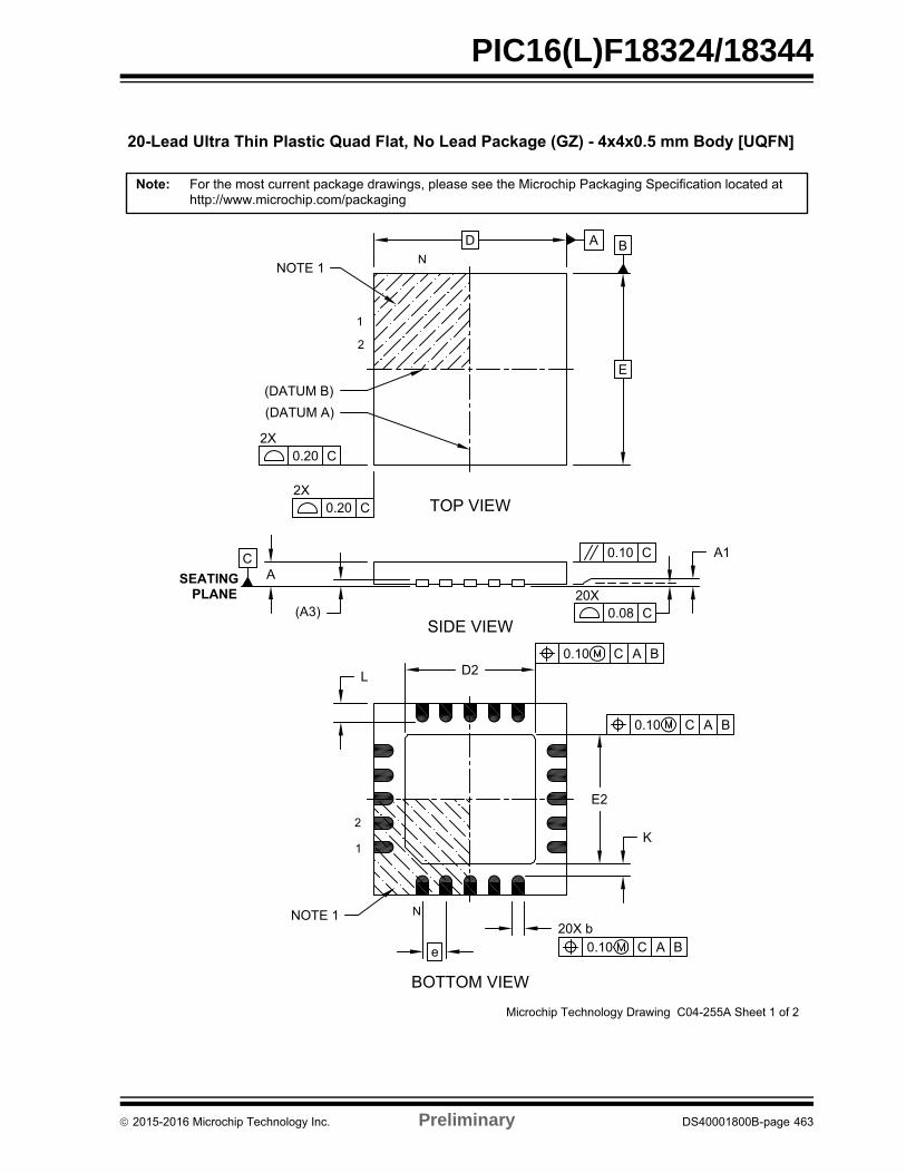
PIC16(L)F18324/18344
BA
0.20 C
0.20 C
0.10 C A B
(DATUM B)(DATUM A)
CSEATING
PLANE
1
2
N
2XTOP VIEW
SIDE VIEW
BOTTOM VIEW
For the most current package drawings, please see the Microchip Packaging Specification located athttp://www.microchip.com/packaging
Note:
NOTE 1
1
2
N
0.10 C A B
0.10 C A B
0.10 C
0.08 C
A1
Microchip Technology Drawing C04-255A Sheet 1 of 2
20-Lead Ultra Thin Plastic Quad Flat, No Lead Package (GZ) - 4x4x0.5 mm Body [UQFN]
D
E
A
(A3)
20X b
e
2X
D2
E2
NOTE 1
L
K
20X
2015-2016 Microchip Technology Inc. Preliminary DS40001800B-page 463
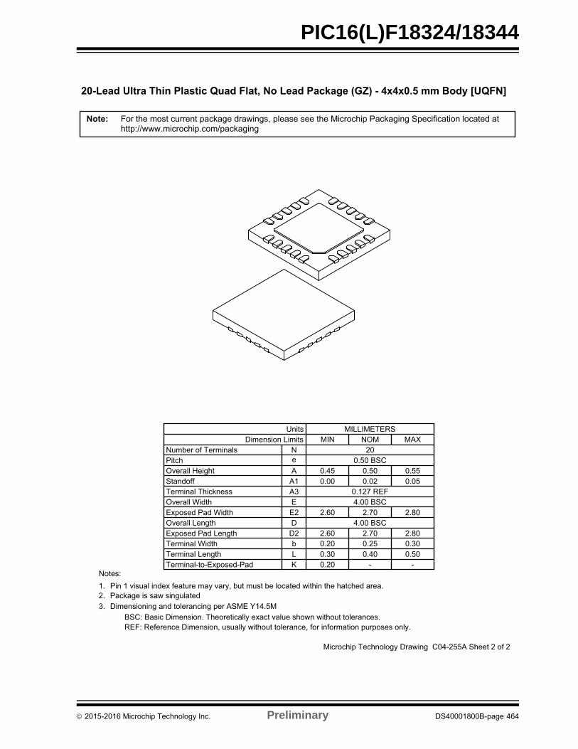
PIC16(L)F18324/18344
Microchip Technology Drawing C04-255A Sheet 2 of 2
For the most current package drawings, please see the Microchip Packaging Specification located athttp://www.microchip.com/packaging
Note:
Number of Terminals
Overall Height
Terminal Width
Overall Width
Overall Length
Terminal Length
Exposed Pad Width
Exposed Pad Length
Terminal Thickness
Pitch
Standoff
UnitsDimension Limits
A1A
b
DE2
D2
A3
e
L
E
N0.50 BSC
0.127 REF
2.60
2.60
0.300.20
0.450.00
0.25
4.00 BSC
0.40
2.70
2.70
0.500.02
4.00 BSC
MILLIMETERSMIN NOM
20
2.80
2.80
0.500.30
0.550.05
MAX
K -0.20 -
REF: Reference Dimension, usually without tolerance, for information purposes only.BSC: Basic Dimension. Theoretically exact value shown without tolerances.
1.2.3.
Notes:
Pin 1 visual index feature may vary, but must be located within the hatched area.Package is saw singulatedDimensioning and tolerancing per ASME Y14.5M
Terminal-to-Exposed-Pad
20-Lead Ultra Thin Plastic Quad Flat, No Lead Package (GZ) - 4x4x0.5 mm Body [UQFN]
2015-2016 Microchip Technology Inc. Preliminary DS40001800B-page 464
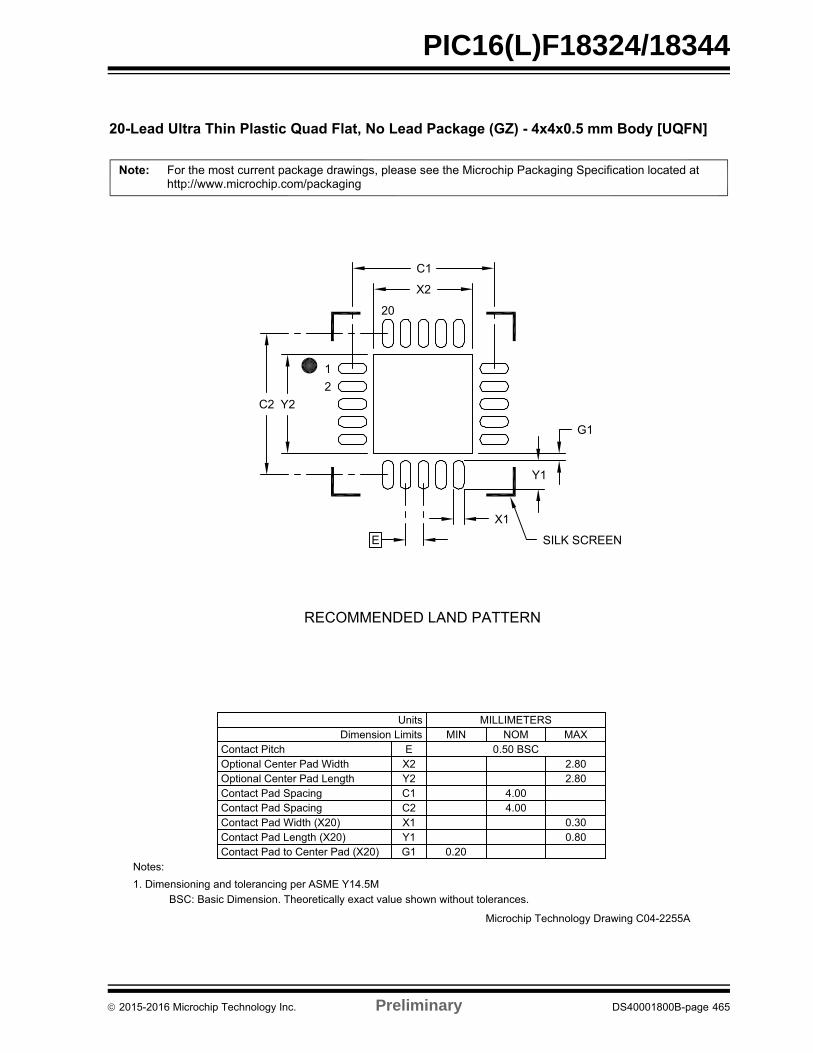
PIC16(L)F18324/18344
RECOMMENDED LAND PATTERN
For the most current package drawings, please see the Microchip Packaging Specification located athttp://www.microchip.com/packaging
Note:
Dimension LimitsUnits
C2
Optional Center Pad Width
Contact Pad Spacing
Optional Center Pad Length
Contact Pitch
Y2X2
2.802.80
MILLIMETERS
0.50 BSCMIN
EMAX
4.00
Contact Pad Length (X20)Contact Pad Width (X20)
Y1X1
0.800.30
BSC: Basic Dimension. Theoretically exact value shown without tolerances.
Notes:1. Dimensioning and tolerancing per ASME Y14.5M
Microchip Technology Drawing C04-2255A
NOM
20-Lead Ultra Thin Plastic Quad Flat, No Lead Package (GZ) - 4x4x0.5 mm Body [UQFN]
SILK SCREEN
12
20
C1
C2
E
X1
Y1
G1
Y2
X2
C1Contact Pad Spacing 4.00
Contact Pad to Center Pad (X20) G1 0.20
2015-2016 Microchip Technology Inc. Preliminary DS40001800B-page 465
2015-2016 Microchip Technology Inc. Preliminary DS40001800B-page 466
PIC16(L)F18324/18344
APPENDIX A: DATA SHEET REVISION HISTORY
Revision A (7/2015)
Initial release of the document.
Revision B (11/2016)
Minor updates brought to Table 1-1; Table 1-2; Table1-3; Added new Chapter 2 “Guidelines for GettingStarted with PIC16(L)F183XX Microcontrollers”;Updated Figure 3-1; Added Section 4.1.1.3 “NVMREGAccess”, Section 4.2.1 “BANK SELECTION”; UpdatedTable 6-1; Updated Figure 7-1; Updated Register 7-6;Updated Figure 8-2; Updated Register 9-1; AddedSection 10.2.4 “WDT IS ALWAYS OFF”; Updated Table11-2; Updated Example 11-4; Removed Example 11-5;Updated Figure 15-1; Updated Figure 18-2; UpdatedFigure 22-1; Updated Figure 29-1; Updated Figure31-1.

2015-2016 Microchip Technology Inc. Preliminary DS40001800B-page 467
PIC16(L)F18324/18344
THE MICROCHIP WEBSITE
Microchip provides online support via our website atwww.microchip.com. This website is used as a meansto make files and information easily available tocustomers. Accessible by using your favorite Internetbrowser, the website contains the following information:
• Product Support – Data sheets and errata, application notes and sample programs, design resources, user’s guides and hardware support documents, latest software releases and archived software
• General Technical Support – Frequently Asked Questions (FAQ), technical support requests, online discussion groups, Microchip consultant program member listing
• Business of Microchip – Product selector and ordering guides, latest Microchip press releases, listing of seminars and events, listings of Microchip sales offices, distributors and factory representatives
CUSTOMER CHANGE NOTIFICATION SERVICE
Microchip’s customer notification service helps keepcustomers current on Microchip products. Subscriberswill receive e-mail notification whenever there arechanges, updates, revisions or errata related to aspecified product family or development tool of interest.
To register, access the Microchip website atwww.microchip.com. Under “Support”, click on“Customer Change Notification” and follow theregistration instructions.
CUSTOMER SUPPORT
Users of Microchip products can receive assistancethrough several channels:
• Distributor or Representative
• Local Sales Office
• Field Application Engineer (FAE)
• Technical Support
Customers should contact their distributor,representative or Field Application Engineer (FAE) forsupport. Local sales offices are also available to helpcustomers. A listing of sales offices and locations isincluded in the back of this document.
Technical support is available through the websiteat: http://www.microchip.com/support
2015-2016 Microchip Technology Inc. Preliminary DS40001800B-page 468
PIC16(L)F18324/18344
PRODUCT IDENTIFICATION SYSTEM
To order or obtain information, e.g., on pricing or delivery, refer to the factory or the listed sales office.
PART NO. X /XX XXX
PatternPackageTemperatureRange
Device
Device: PIC16F18324, PIC16LF18324,PIC16F18344, PIC16LF18344.
Tape and Reel Option:
Blank = Standard packaging (tube or tray) T = Tape and Reel(1)
Temperature Range:
I = -40C to +85C (Industrial)E = -40C to +125C (Extended)
Package:(2) JQ = 16-Lead UQFN (4x4)GZ = 20-Lead UQFN (4x4)P = PDIPST = TSSOPSL = SOICSO = SOICSS = SSOP
Pattern: QTP, SQTP, Code or Special Requirements (blank otherwise)
Examples:
a) PIC16LF18324- I/PIndustrial temperaturePDIP package
b) PIC16LF18344- E/SOExtended temperature,SOIC package
Note 1: Tape and Reel identifier only appears in the catalog part number description. This identifier is used for ordering purposes and is not printed on the device package. Check with your Microchip Sales Office for package availability with the Tape and Reel option.
2: Small form-factor packaging options may be available. Check www.microchip.com/packaging for small-form factor package availability, or contact your local Sales Office.
[X](1)
Tape and ReelOption
-
Note the following details of the code protection feature on Microchip devices:
• Microchip products meet the specification contained in their particular Microchip Data Sheet.
• Microchip believes that its family of products is one of the most secure families of its kind on the market today, when used in the intended manner and under normal conditions.
• There are dishonest and possibly illegal methods used to breach the code protection feature. All of these methods, to our knowledge, require using the Microchip products in a manner outside the operating specifications contained in Microchip’s Data Sheets. Most likely, the person doing so is engaged in theft of intellectual property.
• Microchip is willing to work with the customer who is concerned about the integrity of their code.
• Neither Microchip nor any other semiconductor manufacturer can guarantee the security of their code. Code protection does not mean that we are guaranteeing the product as “unbreakable.”
Code protection is constantly evolving. We at Microchip are committed to continuously improving the code protection features of ourproducts. Attempts to break Microchip’s code protection feature may be a violation of the Digital Millennium Copyright Act. If such actsallow unauthorized access to your software or other copyrighted work, you may have a right to sue for relief under that Act.
Information contained in this publication regarding deviceapplications and the like is provided only for your convenienceand may be superseded by updates. It is your responsibility toensure that your application meets with your specifications.MICROCHIP MAKES NO REPRESENTATIONS ORWARRANTIES OF ANY KIND WHETHER EXPRESS ORIMPLIED, WRITTEN OR ORAL, STATUTORY OROTHERWISE, RELATED TO THE INFORMATION,INCLUDING BUT NOT LIMITED TO ITS CONDITION,QUALITY, PERFORMANCE, MERCHANTABILITY ORFITNESS FOR PURPOSE. Microchip disclaims all liabilityarising from this information and its use. Use of Microchipdevices in life support and/or safety applications is entirely atthe buyer’s risk, and the buyer agrees to defend, indemnify andhold harmless Microchip from any and all damages, claims,suits, or expenses resulting from such use. No licenses areconveyed, implicitly or otherwise, under any Microchipintellectual property rights unless otherwise stated.
2015-2016 Microchip Technology Inc. Prelimin
Microchip received ISO/TS-16949:2009 certification for its worldwide headquarters, design and wafer fabrication facilities in Chandler and Tempe, Arizona; Gresham, Oregon and design centers in California and India. The Company’s quality system processes and procedures are for its PIC® MCUs and dsPIC® DSCs, KEELOQ® code hopping devices, Serial EEPROMs, microperipherals, nonvolatile memory and analog products. In addition, Microchip’s quality system for the design and manufacture of development systems is ISO 9001:2000 certified.
QUALITY MANAGEMENT SYSTEM CERTIFIED BY DNV
== ISO/TS 16949 ==
Trademarks
The Microchip name and logo, the Microchip logo, AnyRate, AVR, AVR logo, AVR Freaks, BeaconThings, BitCloud, CryptoMemory, CryptoRF, dsPIC, FlashFlex, flexPWR, Heldo, JukeBlox, KEELOQ, KEELOQ logo, Kleer, LANCheck, LINK MD, maXStylus, maXTouch, MediaLB, megaAVR, MOST, MOST logo, MPLAB, OptoLyzer, PIC, picoPower, PICSTART, PIC32 logo, Prochip Designer, QTouch, RightTouch, SAM-BA, SpyNIC, SST, SST Logo, SuperFlash, tinyAVR, UNI/O, and XMEGA are registered trademarks of Microchip Technology Incorporated in the U.S.A. and other countries.
ClockWorks, The Embedded Control Solutions Company, EtherSynch, Hyper Speed Control, HyperLight Load, IntelliMOS, mTouch, Precision Edge, and Quiet-Wire are registered trademarks of Microchip Technology Incorporated in the U.S.A.
Adjacent Key Suppression, AKS, Analog-for-the-Digital Age, Any Capacitor, AnyIn, AnyOut, BodyCom, chipKIT, chipKIT logo, CodeGuard, CryptoAuthentication, CryptoCompanion, CryptoController, dsPICDEM, dsPICDEM.net, Dynamic Average Matching, DAM, ECAN, EtherGREEN, In-Circuit Serial Programming, ICSP, Inter-Chip Connectivity, JitterBlocker, KleerNet, KleerNet logo, Mindi, MiWi, motorBench, MPASM, MPF, MPLAB Certified logo, MPLIB, MPLINK, MultiTRAK, NetDetach, Omniscient Code Generation, PICDEM, PICDEM.net, PICkit, PICtail, PureSilicon, QMatrix, RightTouch logo, REAL ICE, Ripple Blocker, SAM-ICE, Serial Quad I/O, SMART-I.S., SQI, SuperSwitcher, SuperSwitcher II, Total Endurance, TSHARC, USBCheck, VariSense, ViewSpan, WiperLock, Wireless DNA, and ZENA are trademarks of Microchip Technology Incorporated in the U.S.A. and other countries.
SQTP is a service mark of Microchip Technology Incorporated in the U.S.A.
Silicon Storage Technology is a registered trademark of Microchip Technology Inc. in other countries.
GestIC is a registered trademark of Microchip Technology Germany II GmbH & Co. KG, a subsidiary of Microchip Technology Inc., in other countries.
All other trademarks mentioned herein are property of their respective companies.
© 2015-2016, Microchip Technology Incorporated, All Rights Reserved.
ISBN: 978-1-5224-1094-2
ary DS40001800B-page 469

2015-2016 Microchip Technology Inc. Preliminary DS40001800B-page 470
AMERICASCorporate Office2355 West Chandler Blvd.Chandler, AZ 85224-6199Tel: 480-792-7200 Fax: 480-792-7277Technical Support: http://www.microchip.com/supportWeb Address: www.microchip.com
AtlantaDuluth, GA Tel: 678-957-9614 Fax: 678-957-1455
Austin, TXTel: 512-257-3370
BostonWestborough, MA Tel: 774-760-0087 Fax: 774-760-0088
ChicagoItasca, IL Tel: 630-285-0071 Fax: 630-285-0075
DallasAddison, TX Tel: 972-818-7423 Fax: 972-818-2924
DetroitNovi, MI Tel: 248-848-4000
Houston, TX Tel: 281-894-5983
IndianapolisNoblesville, IN Tel: 317-773-8323Fax: 317-773-5453Tel: 317-536-2380
Los AngelesMission Viejo, CA Tel: 949-462-9523Fax: 949-462-9608Tel: 951-273-7800
Raleigh, NC Tel: 919-844-7510
New York, NY Tel: 631-435-6000
San Jose, CA Tel: 408-735-9110Tel: 408-436-4270
Canada - TorontoTel: 905-695-1980 Fax: 905-695-2078
ASIA/PACIFICAsia Pacific OfficeSuites 3707-14, 37th FloorTower 6, The GatewayHarbour City, Kowloon
Hong KongTel: 852-2943-5100Fax: 852-2401-3431
Australia - SydneyTel: 61-2-9868-6733Fax: 61-2-9868-6755
China - BeijingTel: 86-10-8569-7000 Fax: 86-10-8528-2104
China - ChengduTel: 86-28-8665-5511Fax: 86-28-8665-7889
China - ChongqingTel: 86-23-8980-9588Fax: 86-23-8980-9500
China - DongguanTel: 86-769-8702-9880
China - GuangzhouTel: 86-20-8755-8029
China - HangzhouTel: 86-571-8792-8115 Fax: 86-571-8792-8116
China - Hong Kong SARTel: 852-2943-5100 Fax: 852-2401-3431
China - NanjingTel: 86-25-8473-2460Fax: 86-25-8473-2470
China - QingdaoTel: 86-532-8502-7355Fax: 86-532-8502-7205
China - ShanghaiTel: 86-21-3326-8000 Fax: 86-21-3326-8021
China - ShenyangTel: 86-24-2334-2829Fax: 86-24-2334-2393
China - ShenzhenTel: 86-755-8864-2200 Fax: 86-755-8203-1760
China - WuhanTel: 86-27-5980-5300Fax: 86-27-5980-5118
China - XianTel: 86-29-8833-7252Fax: 86-29-8833-7256
ASIA/PACIFICChina - XiamenTel: 86-592-2388138 Fax: 86-592-2388130
China - ZhuhaiTel: 86-756-3210040 Fax: 86-756-3210049
India - BangaloreTel: 91-80-3090-4444 Fax: 91-80-3090-4123
India - New DelhiTel: 91-11-4160-8631Fax: 91-11-4160-8632
India - PuneTel: 91-20-3019-1500
Japan - OsakaTel: 81-6-6152-7160 Fax: 81-6-6152-9310
Japan - TokyoTel: 81-3-6880- 3770 Fax: 81-3-6880-3771
Korea - DaeguTel: 82-53-744-4301Fax: 82-53-744-4302
Korea - SeoulTel: 82-2-554-7200Fax: 82-2-558-5932 or 82-2-558-5934
Malaysia - Kuala LumpurTel: 60-3-6201-9857Fax: 60-3-6201-9859
Malaysia - PenangTel: 60-4-227-8870Fax: 60-4-227-4068
Philippines - ManilaTel: 63-2-634-9065Fax: 63-2-634-9069
SingaporeTel: 65-6334-8870Fax: 65-6334-8850
Taiwan - Hsin ChuTel: 886-3-5778-366Fax: 886-3-5770-955
Taiwan - KaohsiungTel: 886-7-213-7830
Taiwan - TaipeiTel: 886-2-2508-8600 Fax: 886-2-2508-0102
Thailand - BangkokTel: 66-2-694-1351Fax: 66-2-694-1350
EUROPEAustria - WelsTel: 43-7242-2244-39Fax: 43-7242-2244-393
Denmark - CopenhagenTel: 45-4450-2828 Fax: 45-4485-2829
Finland - EspooTel: 358-9-4520-820
France - ParisTel: 33-1-69-53-63-20 Fax: 33-1-69-30-90-79
France - Saint CloudTel: 33-1-30-60-70-00
Germany - GarchingTel: 49-8931-9700Germany - HaanTel: 49-2129-3766400
Germany - HeilbronnTel: 49-7131-67-3636
Germany - KarlsruheTel: 49-721-625370
Germany - MunichTel: 49-89-627-144-0 Fax: 49-89-627-144-44
Germany - RosenheimTel: 49-8031-354-560
Israel - Ra’anana Tel: 972-9-744-7705
Italy - Milan Tel: 39-0331-742611 Fax: 39-0331-466781
Italy - PadovaTel: 39-049-7625286
Netherlands - DrunenTel: 31-416-690399 Fax: 31-416-690340
Norway - TrondheimTel: 47-7289-7561
Poland - WarsawTel: 48-22-3325737
Romania - BucharestTel: 40-21-407-87-50
Spain - MadridTel: 34-91-708-08-90Fax: 34-91-708-08-91
Sweden - GothenbergTel: 46-31-704-60-40
Sweden - StockholmTel: 46-8-5090-4654
UK - WokinghamTel: 44-118-921-5800Fax: 44-118-921-5820
Worldwide Sales and Service
11/07/16