from process variations to reliability: a survey of timing
TRANSCRIPT

IPSJ Transactions on System LSI Design Methodology Vol.11 2–15 (Feb. 2018)
[DOI: 10.2197/ipsjtsldm.11.2]
Invited Paper
From Process Variations to Reliability: A Surveyof Timing of Digital Circuits in the Nanometer Era
Bing Li1,a) Masanori Hashimoto2,b) Ulf Schlichtmann1,c)
Received: September 28, 2017
Abstract: In advanced technology nodes, transistors and interconnects with shrinking physical dimensions sufferlarge process variations during manufacturing and are prone to reliability issues. These underlying changes requirean overhaul of the design methodologies for digital circuits. In this paper, we provide an overview of techniquesintroduced recently to analyze the effect of uncertainty in manufacturing and reliability issues of devices due to thediminishing feature size. These techniques range from variation/aging modeling to circuit-level analysis. In addition,active techniques to counter these effects, such as clock skew tuning and voltage tuning are also covered in this paper.
Keywords: timing analysis, process variations, aging, hierarchical timing, clock skew, noise, circuit tuning
1. Introduction
Digital circuits contain two types of gates. Logic gates, e.g.,AND, OR and NOT gates, implement the function of the circuit.The sequential gates, e.g., flip-flops and latches, do not make anycontribution to the logic function directly. Instead, they are usedto synchronize intermediate steps of the computation. An exam-ple of a digital circuit is shown in Fig. 1.
A sequential gate, henceforth with flip-flop as example, is onlyactivated at a given moment to store the data from its input. Ex-cept this exact moment, the stored data and the output of the flip-flop do not change, no matter what happens at its input. Con-sequently, flip-flops sitting on combinational paths in a sequen-tial circuit partition the circuit into separate logic/combinationalfunctional blocks. The data at the outputs of a combinationalblock are latched into the flip-flops connected to them at a givenmoment. Thereafter, any changes at the outputs of the combina-tional block and thus the inputs of the flip-flops do not affect thedata stored inside the flip-flops, until the next latching momentcomes. Since the outputs of flip-flops are connected to the inputsof combinational blocks, the starting time of logic computationcan thus be synchronized.
To coordinate the activities of logic blocks, a clock signal isgenerated and distributed to all flip-flops. The flip-flops are ac-tivated at a clock edge, e.g., the rising clock edge henceforth.Since the clock signal reaches all flip-flops at the same time, thelatching activities of flip-flops trigger signal transitions at the in-puts of logic blocks simultaneously. Because at each rising clockedge new computations are initiated, the performance of a circuitis thus often represented by its clock frequency, indicating how
1 Technical University of Munich, 80333 Munich, Germany2 Osaka University, Osaka, 565–0871 Japana) [email protected]) [email protected]) [email protected]
Fig. 1 Structure of s27 from the ISCAS89 [1] benchmark set.
many input data can be processed in a second by the circuit.To improve circuit performance, the easiest way is to boost its
clock frequency, or, equivalently, shorten the clock period. In2004 the International Technology Roadmap for Semiconductors(ITRS) has predicted that, driven by advances in manufacturingtechnology, the clock frequency would increase by 21% everyyear, jumping from about 2.9 GHz in 2002 to 33.4 GHz in 2015.This optimistic estimation has been, however, adjusted in 2013,predicting that the clock frequency may reach 5.9 GHz in 2015,leading to only 4% annual growth rate. This slowdown of clockfrequency increase is caused by several factors, including processvariations, power consumption, noise as well as reliability andaging issues.
In a digital circuit, the latest time a signal becomes stable isafter it travels through the combinational path with the largest de-lay, called the longest path henceforth. The delay of this pathis equal to the sum of all the delays of logic gates and intercon-nects on the path. These delays are, however, not fixed valuesin reality due to the imperfection in manufacturing processes. Infact, it is not possible to deliver logic gates or interconnects withthe exact design parameters, e.g., physical dimensions, from themanufacturing process. Instead, the parameters of logic gates andinterconnects vary in different chips of the same design, a phe-nomenon called process variations [2], so that some of them have
c© 2018 Information Processing Society of Japan 2
IPSJ Transactions on System LSI Design Methodology Vol.11 2–15 (Feb. 2018)
large delays but others may have small delays.Process variations have been existing since the beginning of
the semiconductor industry. They did not significantly affect thedesign flow in the past because compared with the dimensionsof the logic devices and interconnects, the variations were rela-tively small, so that they could be dealt with by allocating perfor-mance margins easily. In advanced technology nodes, these vari-ations have become relatively large, e.g., reaching a one-sigmavariation of 15.7% in 70 nm manufacturing node [2], so that theycannot easily be compensated anymore by allocating excessiveperformance margins. In addition, local variations have becomemore relevant compared to global variations. Some local vari-ations are purely random–therefore the traditional worst-case-based design methodology cannot properly handle them.
Process variations cannot be determined before real manufac-turing happens and in different manufactured chips their final ef-fects are different. During design phase, timing analysis is stillrequired because designers need to evaluate how the manufac-tured chips perform after experiencing process variations. Con-sequently, the performances of logic gates and interconnects needto be modeled statistically as random variables according to themanufacturing data from foundries, leading to a boom of researchon statistical timing analysis (SSTA) [3].
While the feature size is still being scaled down continuouslyto smaller geometries to enable the development of more com-plex and powerful integrated circuits (ICs) with a higher transistordensity, unfortunately voltage scaling has essentially stopped dueto power limitations, resulting in the breakdown of the DennardScaling concept [4], which specifies that propagation delays inevery new process generation would be reduced by 30%, enablingabout 30% higher frequencies. For example, the first micropro-cessor in 1971, the Intel 4004, ran at 740 kHz. The Intel Pentium4 introduced in 2004 in 90 nm technology was capable of work-ing at 3.4 GHz, leading to a clock speed increased about 4,600times, or roughly 29% annually. In advanced nanometer technol-ogy nodes, leakage power concerns, however, prevent a furtherdownscaling of threshold voltages Vth. Performance could be im-proved by increasing Vdd, which, unfortunately, would result inincreased dynamic power consumption especially in designs witha high clock frequency, and is thus not an option either. Thissituation becomes even more complicated when noise inside thechip is considered, which also demands a large margin in supplyvoltages.
Similar to process variations, another effect that has been ex-isting for years but has become practically relevant since about10 years is aging of transistors as well as the ensuing reliabilityissues. When currents flow through transistors, stress is accumu-lated on them. Gradually, chips may become slower comparedwith the fresh state right after manufacturing. This degradationmay also pose a big challenge in some fields such as automotiveand medical industries, where safety-critical applications requirestable and reliable circuit components. To maintain the desig-nated performance, further timing/voltage margins may need tobe allocated, making the design task more challenging.
In this paper, we survey the state of the art of the researchon timing of digital circuits considering new design challenges
emerging in nanometer manufacturing nodes. These challengesmay lead to significant changes in the long-established designflow for integrated circuits.
2. Timing Constraints
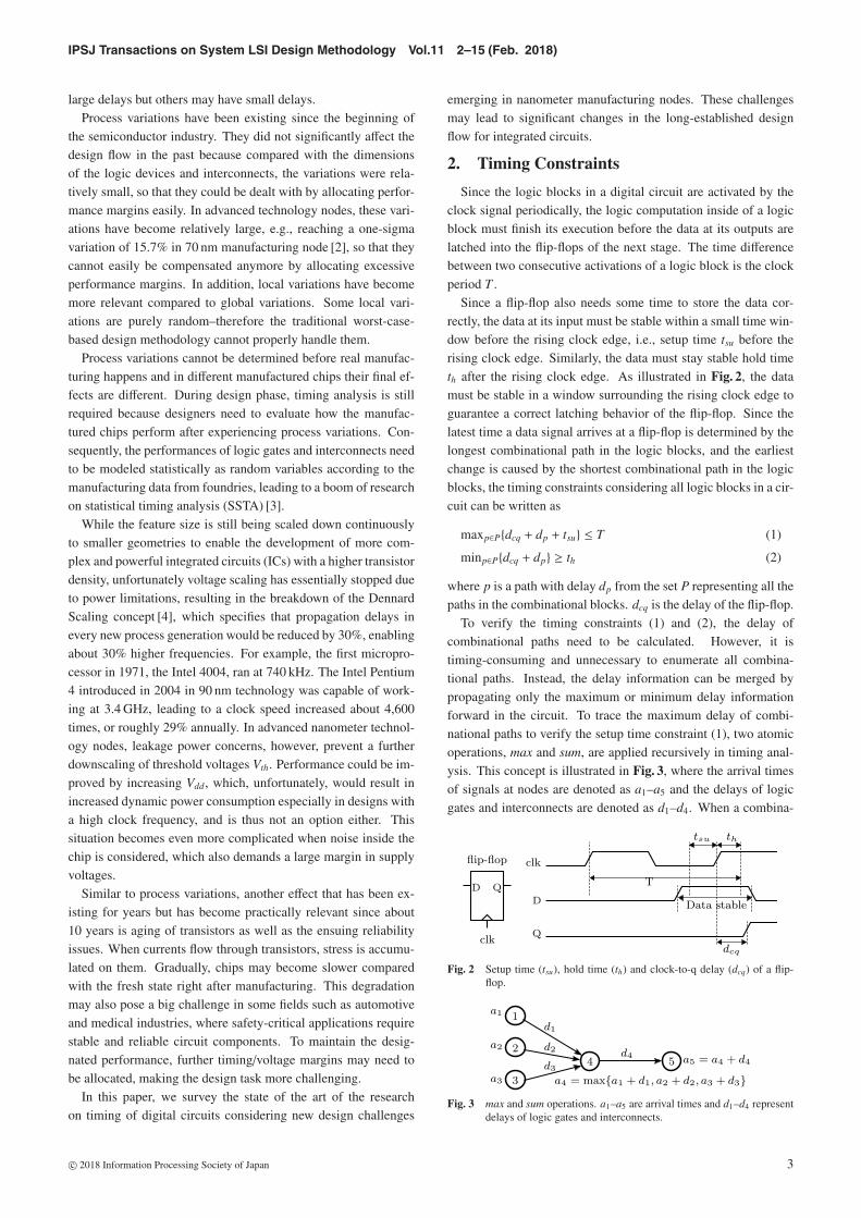
Since the logic blocks in a digital circuit are activated by theclock signal periodically, the logic computation inside of a logicblock must finish its execution before the data at its outputs arelatched into the flip-flops of the next stage. The time differencebetween two consecutive activations of a logic block is the clockperiod T .
Since a flip-flop also needs some time to store the data cor-rectly, the data at its input must be stable within a small time win-dow before the rising clock edge, i.e., setup time tsu before therising clock edge. Similarly, the data must stay stable hold timeth after the rising clock edge. As illustrated in Fig. 2, the datamust be stable in a window surrounding the rising clock edge toguarantee a correct latching behavior of the flip-flop. Since thelatest time a data signal arrives at a flip-flop is determined by thelongest combinational path in the logic blocks, and the earliestchange is caused by the shortest combinational path in the logicblocks, the timing constraints considering all logic blocks in a cir-cuit can be written as
maxp∈P{dcq + dp + tsu} ≤ T (1)
minp∈P{dcq + dp} ≥ th (2)
where p is a path with delay dp from the set P representing all thepaths in the combinational blocks. dcq is the delay of the flip-flop.
To verify the timing constraints (1) and (2), the delay ofcombinational paths need to be calculated. However, it istiming-consuming and unnecessary to enumerate all combina-tional paths. Instead, the delay information can be merged bypropagating only the maximum or minimum delay informationforward in the circuit. To trace the maximum delay of combi-national paths to verify the setup time constraint (1), two atomicoperations, max and sum, are applied recursively in timing anal-ysis. This concept is illustrated in Fig. 3, where the arrival timesof signals at nodes are denoted as a1–a5 and the delays of logicgates and interconnects are denoted as d1–d4. When a combina-
Fig. 2 Setup time (tsu), hold time (th) and clock-to-q delay (dcq) of a flip-flop.
Fig. 3 max and sum operations. a1–a5 are arrival times and d1–d4 representdelays of logic gates and interconnects.
c© 2018 Information Processing Society of Japan 3

IPSJ Transactions on System LSI Design Methodology Vol.11 2–15 (Feb. 2018)
tional component is passed, its delay is added to the arrival time.When multiple arrival times converge at a node, the maximum ofthem is calculated and propagated further. Since logic functionsare not considered, the task of timing analysis becomes merely toefficiently traverse a graph representing the circuit structure anddelays.
3. Timing with Process Variations
In timing analysis, the delays of the longest and shortest pathsshould be calculated to verify Eqs. (1) and (2). In the case thatall gate delays are fixed values, this is not a challenging task.When process variations are considered, however, the computa-tional complexity increases extraordinarily, because the max andsum operations become statistical. Moreover, the results of theseoperations should maintain the correlation to the other randomvariables so that the same formulas of the max and sum opera-tions can be applied recursively. For example, the result a4 ofmax and sum operations at node 4 in Fig. 3 should be representedin the same form as d4 so that the sum operation can be appliedto calculate a5 similarly.
3.1 Process Variation CategorizationProcess variations exist inherently in manufacturing. As the
dimensions of transistors are being scaled down, these variations,however, do not follow the scaling linearly but lag behind thepace. Consequently, the ratio of process variations to the nominaldimensions of devices becomes larger, to the degree of affectingthe delays of logic gates significantly [2]. Since process variationsresult in transistors with dimensions spreading in much larger rel-ative ranges than previously, the delays of logic gates and inter-connects need to be modeled as random variables instead of asfixed values in nanometer manufacturing nodes.
Process variations can be classified into different categories, asshown in Fig. 4. Systematic variations, e.g., the randomness ininterconnect metal thickness, are caused in part by design charac-teristics such as the density of interconnects on a metal layer, sothat they can be extracted and modeled according to the design in-formation even before manufacturing. The variations of this typecan be directly incorporated into post-OPC (Optical ProximityCorrection) timing analysis to improve the accuracy [5].
Non-systematic variations, however, cannot be determined be-fore manufacturing, since they are the results of the inaccuracyin process control during manufacturing. Consequently, they canonly be modeled as random variables when the circuit is designed.Examples of these variations are those in doping density and lay-out independent metal thickness.
Non-systematic variations can be partitioned further into die-to-die variations (interdie variations) and within-die variations(intradie variations) [6]. Die-to-die variations affect all devicesand interconnects on a die equally. For example, the chips inthe center area of a wafer are normally faster than the chips faraway from the center. Within-die variations have different ef-fects on devices or interconnects inside a die, leading to deviationbetween device parameters inside a chip after manufacturing. Ifthe variations of two parameters exhibit no correlation, within-dievariations become a purely random effect, such as the random
Fig. 4 Variation Classification [3].
Fig. 5 Quadtree Correlation Model [8], [9].
distortion caused by lens during photolithography and the purelyrandom variations in doping.
3.2 Correlation ModelingAs discussed above, some components of process variations
may affect more than one device in a chip. Considered as a whole,performances of devices thus exhibit a correlation. Since the un-certainties during manufacturing process vary continuously, pro-cess variations also exhibit a proximity effect, meaning that thesmaller the distance is, the larger the correlation becomes [7].
Several models have been proposed to express the correlationbetween process parameters. The quadtree model in Refs. [8], [9]is illustrated in Fig. 5. In this model, different layers are used torepresent the random components shared by devices in areas ofdifferent scales. For each grid cell, a random variable is assigned.Therefore, the random variable at the top layer models the com-ponent shared by all devices in the chip. As the sizes of gridcells decrease in lower layers, the corresponding variables modelfiner but more locally restricted correlation. This quadtree model,however, does not model the local correlation uniformly. For ex-ample, the distances from (2,4) to (2,1) and to (2,13) are equal. Inthis model, devices in (2,4) and (2,1) share the same variable atlayer 1, but this is not the case for the devices in (2,4) and (2,13).
Another correlation model is proposed in Ref. [10] and is illus-trated in Fig. 6. In this model, the die area is partitioned into a uni-form grid with n cells, and a random variable is assigned for eachgrid. The total n random variables are correlated, containing allthe components in Fig. 4. To simplify statistical computations intiming analysis, these variables are decomposed into linear com-binations of independent random variables, using algorithms suchas principal component analysis (PCA) [11]. This correlationmodel is very flexible, because it can handle any correlation be-tween process parameters rather accurately. This model is revisedin Ref. [12] where hexagonal grid cells are used to partition thedie area.
c© 2018 Information Processing Society of Japan 4

IPSJ Transactions on System LSI Design Methodology Vol.11 2–15 (Feb. 2018)
Fig. 6 Uniform Grid Correlation Model [10].
The correlation models discussed above are all first-orderand only sufficient to model the dependency between Gaussianrandom variables. To incorporate dependency information ofa higher order, methods like independent component analysis [13]have been applied, as in Refs. [14], [15].
3.3 Statistical Timing AnalysisWith random variables representing process parameters de-
composed into linear combinations of independent random vari-ables, the delay of a gate can also be expressed similarly. Forexample, the canonical delay model in Ref. [16] expresses twogate delays as
A = a0 +
n∑i=1
aivi + arvra (3)
B = b0 +
n∑i=1
bivi + brvrb (4)
where vra and vrb are random variables representing the purelyindependent variations of the gate delays. vi are independent ran-dom variables from decomposition shared by all gate delays. a0,b0, ai, bi, ar and br are constant coefficients of the decomposedcomponents, indicating how much a delay is affected by them.The sharing of decomposed components establishes the correla-tion between two gate delays as
Cov(A, B) =n∑
i=1
aibiCov(vi, vi) =n∑
i=1
aibiσ2vi. (5)
During statistical timing analysis, the sum of A and B is com-puted easily as
A + B = (a0 + b0) +n∑
i=1
(ai + bi)vi + (arvra + brvrb )
= s0 +
n∑i=1
sivi + srvrs (6)
where sr is computed by matching the variances of srvrs andarvra + brvrb .
The computation of the maximum of A and B, denoted asmax{A, B}, is, however, more challenging. In Ref. [16], the con-cept of tightness probability (TP) is introduced to represent theprobability a variable is greater than another. When A and B areassumed as Gaussian, TP can be computed as
TP = Prob{A ≥ B} = Φ(
a0 − b0
θ
)(7)
where Φ is the cumulative distribution function of the standard
Gaussian distribution. θ =√σ2
A + σ2B − 2Cov(A, B), with σ2
A and
σ2B denoting the variances of A and B respectively.According to Ref. [17], the mean (μ) and variance (σ2) of
max{A, B} can be computed by
μ = TPa0 + (1 − TP)b0 + θφ(a0−b0θ
) (8)
σ2 = TP(σ2A + a2
0) + (1 − TP)(σ2B + b2
0)
+ (a0 + b0)θφ( a0−b0θ
) − μ2 (9)
where φ is the probability density function of the standardGaussian distribution.
In order to apply the max and sum operations iteratively topropagate arrival times, max{A, B} is approximated in the canon-ical linear model as
max{A, B} ≈ m0 +
n∑i=1
mivi + mrvrm (10)
where m0 is equal to μ. mi is computed by mi = TPai+ (1−TP)bi.mr is computed by matching the variance of the linear formEq. (10) and σ2 in Eq. (9).
The example above has exposed the difference between statis-tical timing analysis (SSTA) and traditional static timing analysis(STA). In STA, the maximum of two arrival times is only a sim-ple comparison of two numbers. But in SSTA, it involves a lotcomputation not only for the mean and the variance of the re-sult but also for the linearized expression Eq. (10), which mustguarantee that the approximation form maintains the correlationbetween max{A, B} and any other variable so that the max andsum computations can be applied recursively during arrival prop-agation with the same formulas as in Eqs. (6)–(10) [10], [16]. Thesum operation Eq. (6) is easier but is still computationally muchmore demanding compared to the sum of two simple numbers inSTA. This complexity makes SSTA relatively slow and thus hashampered its application in industrial design flows.
The linear timing analysis methods above assume that gate de-lays are approximated as Gaussian random variables. This lim-itation has been relaxed in Refs. [18], [19], [20] by representingtiming properties as quadratic functions of independent Gaussianrandom variables. Furthermore, gate delays can also been ex-pressed as linear combinations of non-Gaussian variables, as inthe method in Refs. [14], [15], while the method in Ref. [21] pro-poses a general framework to incorporate linear/nonlinear com-binations of Gaussian and non-Gaussian random variables.
The methods above are block-based because at each compo-nent only the maximum or minimum of the variables is propa-gated. Path-based methods have also been explored for statisticaltiming analysis, e.g., in Refs. [22], [23]. These methods can onlyprocess a given set of combinational paths, which, however, arestill not easy to identify accurately from the circuit [24].
3.4 Hierarchical Statistical Timing AnalysisTo counter the immense computational effort required for tim-
ing analysis considering process variations, hierarchical statisti-cal timing analysis has been investigated to accelerate system-level timing analysis.
Hierarchical timing analysis splits timing analysis into two
c© 2018 Information Processing Society of Japan 5

IPSJ Transactions on System LSI Design Methodology Vol.11 2–15 (Feb. 2018)
Fig. 7 Timing paths in timing model extraction.
steps. At first, timing properties inside submodules are extractedindividually. Afterwards, the timing models of all the submod-ules in a circuit are combined together to perform timing analysisof the whole design.
A timing model contains interface timing information ofa module, which is unusually the delay information of: 1) directpaths from inputs to outputs, type A in Fig. 7; 2) paths from in-puts that can reach a flip-flop or a latch inside the module, type B;3) paths from an internal flip-flop or a latch to an output, type C;4) paths between flip-flops or latches, type D.
For static timing analysis without consideration of processvariations, timing model extraction has been explored in Ref. [25]to extract black-box models, which only contain interface tim-ing information. The methods in Refs. [26], [27], [28], [29] ap-ply graph transformation operations to merge nodes and edgesrepresenting the timing information of the original circuit, lead-ing to gray-box timing models because timing information insidethe modules is exposed. For sequential circuits, Interface LogicModel (ILM) in Ref. [25] keeps all the combinational paths be-tween input ports to the first-level flip-flops and from the last-level flip-flops to the output ports. The Extracted Timing Model(ETM) [25], however, collapses all such paths to reduce the sizeof timing models, sacrificing the flexibility of keeping the origi-nal parasitics information associated with the original logic gatesand interconnects. For latch-based circuits, all latches can be re-tained in the timing model as in Ref. [27], or the depth of trans-parency from the input ports to internal latches and from the in-ternal latches to the output ports are assumed as given [30], sothat the number of latches potentially traveled transparently canbe determined.
When process variations are considered, timing model extrac-tion methods for combinational circuits and sequential circuitswith flip-flops in Refs. [25], [26], [27], [28], [29] can be ap-plied similarly, but with the maximum and sum computationsreplaced by the corresponding statistical versions. For sequen-tial circuits with latches, the depth of transparency becomes sta-tistical [31], [32]. Therefore, timing models should be extractedwith respect to the probabilities of transparency depths [33], [34],which are affected by the statistical path delays in the originalcircuit.
When integrating extracted statistical timing models into tim-ing analysis of the whole circuit, a special challenge should bemet when process variations are considered. At the top level, thedie area occupied by each module is partitioned to model the cor-relation between variations when generating timing models, suchas using the uniform grid in Ref. [10]. When the extracted models
Fig. 8 Grid partition of the chip in hierarchical statistical timing analysis.
Fig. 9 Problem of timing analysis for sequential circuits considering dy-namic power supply noise.
are placed together, the grids inside them may not be aligned, asillustrated in Fig. 8. Therefore, the relation between these gridsshould be established. In Refs. [35], [36], this problem is ad-dressed by linear transformation between the coefficients of in-dependent random variables. But there might be no solution fromthis method if the transformation matrix is not selected properly.This method is improved in Refs. [34], [37] by using the coeffi-cient matrices of submodules and the top grid directly.
3.5 Clock Skew and Jitter Aware Setup and HoldVerification
3.5.1 Setup and Hold VerificationSlack computation for setup and hold constraints can be ex-
plained using Fig. 9, where slack is the timing margin betweenrequired signal arrival time to meet timing constraints and actualarrival time. All arrival times and element delays are supposed tobe expressed and computed with the canonical form Eq. (3).
First, the procedure to calculate slack for setup constraint isexplained as follows.( 1 ) Take the source of clock network as an origin, and set the
arrival time at the clock source to 0. Then perform SSTA,and obtain the latest arrival time t1 at input D of each FF.Here, the clock signal propagates to the combinational cir-cuit through CLK-to-Q path in FFs, and hence each FF is re-garded as a combinational cell, and CLK-to-Q delay is addedto the arrival time.
( 2 ) Take the clock source as an origin and set the arrival time atthe clock source to clock cycle T . Then obtain the arrivaltime t2 at clock input CLK of each FF.
( 3 ) Slack for setup constraint Ssu is calculated for every FF.
Ssu = t2 − t1 − Tsu (11)
where Tsu is the setup time of the FF.Similarly, slack for hold constraint can be computed with the
following procedure.
c© 2018 Information Processing Society of Japan 6

IPSJ Transactions on System LSI Design Methodology Vol.11 2–15 (Feb. 2018)
Fig. 10 An example of structural correlation in slack computation.
( 1 ) Take the clock source as an origin, and set the arrival timeat the clock source to 0. Then perform SSTA, and obtain theearliest arrival time t3 at input D of each FF. The arrival timet4 at clock input CLK of each FF is also computed.
( 2 ) Slack for hold constraint Shold is calculated for every FF.
Shold = t3 − t4 − Thold (12)
where Thold is the hold time of the FF.3.5.2 Common Path Pessimism
When two arrival times that share common paths are maxedor subtracted, this structural correlation should be considered.This situation arises when setup and hold slacks are computedby subtracting two arrival times of launch and capture paths ateach FF because both the launch and capture paths share someclock buffers and the common path inherently exists. The prob-lem arises from subtractions t2 − t1 in Eq. (11) and t4 − t3 inEq. (12). The path corresponding to t2 partially overlaps the pathsof t1 inside the clock distribution network (CDN).
Let us examine a simple example of Fig. 10. For simplicity,this example assumes all variations are static and uncorrelated. Inthis case, μ(t1), σ(t1), μ(t2) and σ(t2) are estimated to be 110 ps,6.6 ps, 120 ps and 5 ps respectively, and Tsu is 0 ps. When Eq. (11)is computed without considering the common path, μ(Ssu) andσ(Ssu) are 10 ps (= 120 − 110) and 8.3 ps (=
√52 + 6.62). In con-
trast, the correct μ(Ssu) and σ(Ssu) considering the common pathare 10 ps and 4.2 ps. In this case, the correct values are estimatedby virtually eliminating the leftmost inverter, namely, μ(t1), σ(t1),μ(t2) and σ(t2) becomes 60 ps, 4.2 ps, 70 ps and 0 ps respectively.Ignoring the structural correlation over-estimates the standard de-viation by 98%.
Common path pessimism reduction has been studied to tacklethis common path problem. References [38], [39] proposesa method to solve this problem from the viewpoint of path-basedanalysis. First, the authors determine a target path for timing ver-ification, and they obtain the pair of FFs which are the source andsink of the path. Next, the clock distribution network is tracedfrom the FFs to the clock source, and the branching point of theclock paths of the FFs is found. Finally, by regarding the meetingpoint as the source of clock signal, the common path is elim-inated and setup and hold verification is performed. However,these path-based methods may suffer from excessive CPU timewhen the number of the candidates for critical path is large.
On the other hand, the block-based analysis, which does notsuffer from the number of paths, can cope with common pathsby increasing the number of random variables [40]. Let us ana-lyze Fig. 11 and calculate arrival times t1 and t2 as an example.In this situation, both t1 and t2 contain the delays of cba and cbb
in common, which causes the structural correlation problem. To
Fig. 11 Partial structure of general sequential circuit.
cope with this problem involved in the slack computation, indi-vidual random variables are assigned to each clock driver. As anexample, assume a case that each clock buffer cba, cbb, and cbc
has its random variable vcba , vcbb , and vcbc . By extending Eq. (3)with vcba , vcbb , and vcbc , t1 and t2 are expressed in Eqs. (14) and(16).
t1 = a1,0 +
m∑j=1
a1, jv j + a1,rvr1 (13)
+c1,avcba + c1,bvcbb + c1,cvcbc (14)
t2 = a2,0 +
m∑j=1
a2, jv j + a2,rvr2 (15)
+c2,avcba + c2,bvcbb + c2,cvcbc (16)
where vr1 and vr2 are the random variables to represent randomcomponents of the gates except the clock buffers, and c1,[a−c]
and c2,[a−c] are the coefficients which represent the magnitudesof vcb[a−c] in t1 and t2 respectively. In this example, c2,c is 0. Here,t2 can be obtained by summing the delays of cba and cbb. On theother hand, all paths to the D terminal of the topmost FF includecba, and hence t1 includes the delay of cba. In this case, c1,a andc2,a are identical, which means that the terms of vcba in t1 and t2 arecanceled out when t2 − t1 is computed. By this way, the structuralcorrelation is considered automatically thanks to the assignmentof individual random variables to clock drivers.
When the analyzed circuit is large, the number of random vari-ables could be a problem in terms of SSTA run time and memory.However, this problem can be mitigated exploiting the tree struc-ture of the CDN. In the CDN, the clock drivers in the upstreamnetwork are often included in the common path. On the otherhand, the number of upstream drivers is much smaller than thatof downstream drivers. Therefore, assigning random variables toclock drivers from the clock source with breadth first search, aslong as the computational cost permits, efficiently mitigates theproblem of the structural correlation. If the available computa-tional resources are large enough, each clock driver has its ownrandom variable respectively, which can achieve a full consider-ation of the structure correlation on CDN. On the other hand,structural correlation is also largely considered even if randomvariables are assigned only to the upstream drivers because theyare shared by downstream components.
Figure 12 shows the accuracy of setup slack estimation andSSTA run time. The cases of 1 and 2019 random variable(s) cor-respond to (M1) and (M2), respectively. There is a tradeoff be-tween accuracy and run time. As the number of random variablesincreases, the worst setup slack defined as μ + 3σ converges and
c© 2018 Information Processing Society of Japan 7

IPSJ Transactions on System LSI Design Methodology Vol.11 2–15 (Feb. 2018)
Fig. 12 SSTA accuracy and run time versus # of random variables associ-ated with clock drivers.
Fig. 13 Statistical noise modeling for taking into consideration clock skewand jitter.
SSTA run time increases. It can be seen that a small number ofrandom variables, such as 10, attain the worst setup slack closewithin 0.1 ps to that with more than 2,000 variables. In this case,individual random variables are assigned to the first three stagedrivers, and the increase in SSTA run time from (M1) is only0.4%.3.5.3 Impact of Supply Noise on Timing
Power supply noise varies in every clock cycle depending oncircuit workload, and hence delay variation due to supply noise isdifferent temporally. In addition, non-uniform circuit switchingsin space and topology of power distribution network make sup-ply noise different in space. Therefore, clock arrival time variesin time and space, which causes clock jitter and clock skew.
Such impact of supply noise on timing can be consideredconsistently by adding random variables modeling noise intoEq. (3) [40], [41]. Let us explain the statistical noise model usingFig. 13. To express dynamic waveforms within a cycle, a clockcycle is partitioned into several time spans, and a representativevoltage, e.g., average is computed. Afterwards, a random variableis assigned to power supply or ground voltage at each time spanand at each spatial grid. The voltage value at every clock cycle istreated as a different sample. Figure 13 shows an example whenthe voltage at position (x, y) is divided into five time spans and itsrandom variables are denoted as Vx,y,0 to Vx,y,4. To compute Ssu inEq. (11), the correlation between noise waveforms of successiveclock cycles need to be taken into consideration. Reference [42]points out that this correlation contributes to mitigate timing vio-lation even though large clock jitter arises due to resonant powersupply noise. To consider the correlation and compute Ssu ap-propriately, the origin of temporal division is set to the clocklaunch timings at the source of the CDN. The sample, whichis divided into several time spans, is extended in time so that theclock and signal propagations both in the launch path (t1) and
Fig. 14 Delay curves of a flip-flop. (a) Curves of setup/hold slack combina-tions with respect to different constant clock-to-q delays. Setup andhold slacks are the time differences between the signal switches andthe clock edge. (b) Characterization point of setup time and holdtime in traditional STA.
the capture path (t2) are included in a single sample. Therefore,a correlation between the variables of successive clock cyclessuch as between Vx,y,0 and Vx,y,3 in Fig. 13 is naturally considered.With this modeling, the correlation between noise waveforms ofsuccessive clock cycles, which is demanded to accurately com-pute Ssu in Eq. (11), can be appropriately modeled.
3.6 Timing with Setup-Hold Time InterdependencyProcess variations may affect path delays in a sequential cir-
cuit statistically. If the delay of a path in a manufactured chipexceeds the clock period minus the setup time of a flip-flop, a tim-ing violation is assumed to happen. In reality, however, the datamay still be latched into the flip-flop correctly even in view ofa violation of the setup time constraint (1), but the clock-to-q de-lay may increase significantly, leading to a delay increase of thecombinational paths of the next stage. If those paths are short,the increased delay can be absorbed automatically. As shownin Fig. 14 (a), a flip-flop can work with different setup-hold timecombinations with different clock-to-q delays. In the traditionaldefinition, the setup time and hold time are simply approximatedas the point A in Fig. 14 (b), losing the flexibility of the flip-flopcompletely.
The setup-hold interdependency has been investigated inRefs. [43], [44] to exploit the compensation between setup timeand hold time combinations with respect to a given clock-to-qdelay. In addition, a method based on Euler-Newton tracing isintroduced in Refs. [45], [46] to characterize the delay curves offlip-flops. These methods, however, do not consider the relationbetween clock-to-q and setup/hold times, leading to a limited per-formance improvement. To remove this limitation the method inRef. [47] uses a quadratic programming model to calculate theoptimal clock period directly, but it is incapable of solving thehigh-order programming problem for large circuits. To simplifythe three dimensional model, the method in Ref. [48] applies ananalytic function and calculates the minimum clock period by it-erations. In addition, the method in Ref. [49] approximates thethree dimensional delay surface using linear planes. In calcu-lating the minimum clock period of a circuit, this method, how-ever, splits the problem into two-dimensional problems. Further-more, the method in Ref. [50] proposes an efficient algorithm tocapture timing violations in a circuit very efficiently, but onlythe relation between clock-to-q delay and setup slack is con-sidered in this method. Most recently, the method in Ref. [51]
c© 2018 Information Processing Society of Japan 8

IPSJ Transactions on System LSI Design Methodology Vol.11 2–15 (Feb. 2018)
Fig. 15 Aging graph pruning [53] of the ISCAS85 circuit c17 depicted in (a). Timing graph of this circuitand the reduced graph are shown in (b) and (c), respectively.
models the delay surface using piecewise polygons and performsthe timing analysis using integer linear programming togetherwith reduction techniques. In addition, process variations areconsidered together with setup-hold interdependency for flip-flopmodels in Ref. [52], but how to incorporate the generated statisti-cal models in statistical timing analysis is still open.
4. Aging
With the diminishing dimensions of devices, a new challengethat has been around for a long time, aging of ICs, has also startedto attract increasing attention since about 10 years. The term “ag-ing” covers a number of effects impacting devices in nanome-ter manufacturing nodes, most prominently Hot Carrier Injec-tion (HCI), Negative Bias Temperature Instability (NBTI), Elec-tromigration (EM) and Time-Dependent Dielectric Breakdown(TDDB). Moreover, Positive BTI (PBTI) is also increasingly be-coming a consideration. For example, NBTI and HCI result in anincrease of Vth or decrease of Ion, respectively, causing a loss ofperformance, up to 20% over time.
With aging the performance of devices deteriorates over time.The analysis of aging effects is challenging, since the amountof aging depends on a number of factors, among which are Vdd,Temperature, frequency and also the amount of switching or thespecific voltage level a transistor experiences. Accordingly, boththe specific structure of a circuit and its real usage contribute tothe results of aging. Aging analysis is further complicated by thefact that NBTI degradation partly recedes once a stress conditionis removed. This phenomenon is known as “recovery effect.”
Aging analysis traditionally has focused on potential effect ofaging on individual transistors. As a result of such transistor anal-ysis, an overall safety margin was added into the timing signoffto guarantee the correct functionality of the chips. This coarse-grained approach is increasingly less feasibly because, on the onehand, aging has become more pronounced, and on the other hand,the timing budget is becoming increasingly tight, thus not beingable to tolerate a large timing margin anymore. Consequently, ithas become desirable to analyze the aging effect of a given circuitspecifically to provide more fine-grained information.
To calibrate aging effects, transistor-level simulation is re-quired. Though traditional transistor aging models are accurate,they are too slow for analyzing large ICs. To solve this problem,research has been undertaken to analyze HCI and NBTI and thefactors influencing them, and to develop timing models and algo-rithms for aging analysis on gate level, leading to a speedup ofaging analysis by orders of magnitude [54], [55], [56], [57], [58],
[59], [60], [61]. The AgeGate model [53], [62], [63] is probablystill the state of the art in gate-level aging analysis today. Thisaging model can handle both HCI and NBTI. It is independentof the current use profile, defined by Vdd and temperature T overthe lifetime of the IC. It also incorporates the aging effect of eachtransistor in a gate individually and the aging of output slope,both of which are required for accurate timing analysis. The ap-proach of AgeGate builds on the canonical delay model [16] sothat it can be integrated into standard industrial STA-based tim-ing signoff flows smoothly [64].
The AgeGate model was extended later to take module-levelaging analysis into account, speeding up aging analysis further,while maintaining a good accuracy [65]. This approach extractsa timing graph of a module from the original gate-level netlist.Thereafter, the graph is pruned significantly. For example, anypath that can never become critical under aging and process vari-ations is not considered in the analysis. The concept of this prun-ing is illustrated in Fig. 15. Empirical results have confirmed thatthe number of timing paths can be reduced by up to four ordersof magnitude or even more for aging analysis. The reduced tim-ing graphs of modules can not only be used to accelerate aginganalysis, but also to identify critical paths to be monitored on-line, hence enabling a systematic design approach by combiningperiodic monitoring of a circuit during its operation and onlinetuning.
Similar to statistical timing analysis, the characterization of ag-ing still aims to capture more detailed delay information of logicgates for timing analysis in the current design flow. During thedesign phase, aging effect still have to be considered statisticallysince both process variations and aging affect manufactured chipsindividually and produce different critical paths in different chipsafter manufacturing. To counter the aging effects actively, post-silicon tuning techniques can also be applied to adjust the timingproperties of individual chips. Techniques in this category in-clude body bias tuning [66], [67], voltage control [68], [69], [70]as well as clock tuning [71], [72], [73].
5. Circuit Tuning
While process variations must be modeled as random variablesduring the design phase, their effects become fixed in individ-ual chips after manufacturing. These chips have different perfor-mance because process variations affect them differently. Sim-ilarly, aging is also a temporal effect of individual chips. Tocounter these effects actively, manufactured chips maybe tunedaccordingly.
c© 2018 Information Processing Society of Japan 9

IPSJ Transactions on System LSI Design Methodology Vol.11 2–15 (Feb. 2018)
Fig. 16 Post-silicon delay tunable buffer in Ref. [71].
5.1 Post-silicon Clock TuningA representative post-silicon tuning technique is clock skew
tuning. In a sequential circuit, the clock signal reaches all flip-flops at the same moment. With this strict assumption, the perfor-mance of the circuit is determined by the longest path in the cir-cuit, no matter how fast the other paths are. To balance the perfor-mance between different paths, clock edges can be tuned towardfast paths so that slow paths receive more timing budget to finishtheir signal propagation to improve the overall yield [74], [75].
There are various structures of post-silicon clock tuning [71],[76], [77], [78]. For example, the delay buffer in Ref. [71] isillustrated in Fig. 16, where the delay between the clock inputCLK IN and the output CLK OUT is controlled by the values ofthree registers configured through the test access port (TAP).
To perform post-silicon clock tuning, delay buffers should beinserted into the circuit during the design phase. Since thesebuffers occupy die area, a tradeoff should be made to balancethe yield improvement and the enlarged area. When decidinghow many buffers to insert into a circuit, the method in Ref. [79]presents a technique based on clock scheduling to balance theskews resulting from process variations. In Ref. [80] this problemis solved using a graph-based algorithm. In Ref. [72] several al-gorithms are proposed to insert buffers into the clock tree to guar-antee a given yield and minimize the total area taken by these tun-able buffers. Furthermore, the methods in Refs. [81], [82] solvesthis problem with a sampling-based method to recognize a lim-ited number of locations to insert tunable buffers for yield im-provement, while the computational complexity of this method isreduced using machine learning in Ref. [83]. In Ref. [84], thisproblem is solved together with gate sizing. In Ref. [85], theplacement of tunable buffers is explored and a considerable yieldimprovement has been observed.
After manufacturing, the tunable buffers should be configuredto adjust the clock skews in the manufactured chips. This configu-ration requires that delay information should be captured for thesechips. In Ref. [73], this post-silicon configuration is performed bysearching a configuration tree together with graph pruning andbuffer grouping. In Refs. [86], [87] path delays are measured in-dividually in manufactured chips and delay buffers are tuned ac-cordingly. Since this individual measurement is not efficient, sta-tistical prediction and aligned delay test have been introduced inRef. [88]. Furthermore, in Refs. [89], [90], post-silicon tuning isapplied for online adjustment to counter aging effect. Moreover,in Ref. [91] this method is applied to compensate dynamic delayuncertainty induced by temperature variations.
Fig. 17 Pre-ordered compensation via body biasing.
5.2 Body Bias TuningPost-silicon performance can also be tuned by supply voltage
scaling or body biasing. Various supply voltages can be providedby an external voltage regulator or an on-chip DC-to-DC con-verter. Here, low impedance distribution of multiple supply volt-ages is a burden to physical design. On the other hand, generationand distribution of body voltages are relatively easier comparedto those of supply voltage, because the flowing current is verysmall.
Traditionally, chip-level and block-level tuning have been stud-ied and adopted in some commercial chips. On the other hand, toimprove timing while keeping power dissipation low, fine-grainedtuning only for regions with timing violation is effective, sincemost other regions in fabricated chips and blocks do not violatetiming specification. However, fine-grained tuning involves animplementation overhead, because of the need of proper separa-tion and distribution of multiple body and supply voltages, as wellas level shifters. All of them need extra area and/or power dissi-pation. The finest granularity is the logic gate, but the overhead isimpractically huge and therefore not acceptable. Another prob-lem of fine-grained tuning is the test cost required to obtain anoptimal tuning result after fabrication. If there are M tuning vari-ables and each variable can take N values, the number of combi-nations is NM , and finding an optimal combination for every chipafter fabrication becomes less practical, as M and N increases.
To minimize power dissipation after post-silicon tuning withacceptable implementation overhead, gate clustering has beenproposed [92]. The goal of this approach is to attain a tuningquality that is close to gate-level tuning while reducing the im-plementation overhead and the number of tuning variables M toM′ ( M). Although the number of combinations is reducedto NM′ , the test cost is still expensive for most products, whichprevents post-silicon tuning.
To further reduce the test cost, Ref. [93] proposes to preset thetesting order of combinations during design time. This worklimits N = 2, and determines an ordered cluster set that al-lows only M + 1 combinations for test and guarantees mono-tonic decrease/increase in delay/power irrelevant of manufactur-ing variability (Fig. 17), where this monotonicity results from thefact that changing a region with more FBB while the other re-gions unchanged must reduce delay and increase power. Thanksto this monotonic leveling and limitation of the number of lev-els, the test cost of post-silicon tuning is significantly reduced.
c© 2018 Information Processing Society of Japan 10

IPSJ Transactions on System LSI Design Methodology Vol.11 2–15 (Feb. 2018)
Fig. 18 Error prediction based adaptive voltage scaling.
Reference [94] extends this pre-order body biasing to multiplebias voltages. During the body bias clustering, this method ex-plicitly estimates and minimizes the average leakage after thepost-silicon tuning. Experimental results in Ref. [94] demonstratethat this method reduces the average leakage by 25.3 to 51.9%compared to the non-clustering case. It is also revealed that twobias voltages are sufficient when only a small number of compen-sation levels are allowed for test cost reduction.
5.3 Monitoring and Dynamic (Online) Tuning5.3.1 Opportunities and Challenges
To minimize design and operating margins, adaptive circuit de-sign is promising where each chip self-adjusts its operating con-dition, such as supply voltage and body bias. Run-time adapta-tion can cope with dynamic environmental fluctuation and agingin addition to static process variations. The most popular adap-tation is adaptive voltage scaling (AVS). There are two AVSstrategies in literature; error detection and recovery based con-trol (e.g., Razor [95]), and error prediction and prevention basedcontrol (e.g., canary FF [96], [97], slack monitor [98], timing er-ror predictive FF (TEP-FF) [99] *1). In both strategies, sensors areembedded to detect/predict timing errors, and the supply voltageis controlled according to the sensor outputs.
Figure 18 shows a circuit that adaptively controls the speedand power dissipation using a warning signal generated by a TEP-FF [99]. The TEP-FF consists of a normal flip-flop, a delay bufferand a comparator (XOR gate). When the timing margin is grad-ually decreasing, a timing error occurs at the TEP-FF before themain FF captures a wrong value due to the delay buffer, whichenables us to predict that the timing margin of the main FF is notlarge enough. A warning signal is generated to predict the timingerrors.
Let us focus on timing margin degradation due to aging. Fig-ure 19 illustrates how the operational margin in the chip lifetimevaries with and without adaptation. Without adaptation, the oper-ational margin at the beginning of the chip lifetime is large, andthe margin decreases as the chip ages. If the delay increase due toaging exceeds the timing margin, timing errors occur in the chip.This time to the first error corresponds to time to failure (TTF),and TTF varies depending on chip operating environment, work-load and process variations. Mean TTF (MTTF) is often used asa metric of device lifetime and reliability. With adaptation, ide-ally a constant operational margin can be set for the entire chip
*1 There are several names, but the sensor structure is the same.
Fig. 19 Margins of circuits with and without adaptive speed control in chiplifetime.
Fig. 20 Margins of circuits with and without adaptive speed control in chiplifetime.
lifetime. Especially, the margin can be reduced at the beginningof the chip lifetime. If the large operational margin can be trans-lated into supply voltage reduction, the aging process, i.e., theperformance degradation, can be slowed down, and the chip life-time is extended. For pursuing these advantages, performanceadaptation has widely been studied. For example, Ref. [97] re-ports that the power dissipation with performance adaptation issmaller than that with conventional worst-case design by 46% in65 nm subthreshold design.
On the other hand, the negative impact of performance adapta-tion, which is illustrated in Fig. 20 is less studied. Performanceadaptation degrades noise immunity, especially at the beginning,and hence the possibility that an unexpected timing error dueto, for example, unexpected large supply noise occurs becomeshigher. In addition, the margin checking performed in the chip isnot perfect due to the limited area available for test logic or thelimited time allowed for test. Therefore, there is a fundamentalproblem that the possibility of timing error occurrence cannot becompletely reduced to zero, since, for example, a sudden delayincrease larger than expectation can induce a timing error with-out error detection or before error prediction. Similarly, offlinedelay testing may miss the error because delay testing is carriedout with a certain time interval. It should be noted that the timingerrors due to such a sudden delay increase arise even in the chipswithout adaptive speed control, especially at the end of the chiplifetime because the operational margin is small.5.3.2 MTTF Estimation for Design Optimization
To obtain a good adaptive circuit design mitigating the abovenegative impact, the adaptive circuit needs to be optimized. Eachadaptation scheme has some design parameters to optimize andthe built-in test can be tuned. However, it is difficult to eval-uate how much improvement in MTTF and power is achievedby the optimization and tuning, since the device lifetime is
c© 2018 Information Processing Society of Japan 11

IPSJ Transactions on System LSI Design Methodology Vol.11 2–15 (Feb. 2018)
Fig. 21 Overview of stochastic error rate estimation.
Fig. 22 MTTF of CPI circuits.
extraordinarily longer than simulatable time. For example, fora 10 year operation (3 × 10¹⁷ clock cycles) with a logic simulatorprocessing 3×10³ cycles per second, it takes 3×10⁶ years. There-fore, another approach instead of naive simulation is indispens-able. To enable adaptive circuit optimization, a stochastic errorrate estimation method is introduced [99], [100]. The proposedmethod models adaptive speed control under dynamic delay vari-ation as a continuous-time Markov process (Fig. 21), where statesin Markov process are defined such that each state is associatedwith a pair of unintentional delay variation and levels of supplyvoltage. One more failure state is added to represent that a tim-ing error happened in the past. Given a matrix of the transitionrates, closed-form expressions of state probability as a function oftime t can be obtained. This means that once the matrix of tran-sition rates is given, the MTTF computation can be carried outwith a constant time, and the computation time is independent ofthe timing error rate and MTTF of the circuit under evaluation.Consequently, the necessary computation time can be reduced bytwelve orders of magnitude in a test case.5.3.3 MTTF Extension by Critical Path Isolation
The above MTTF estimation enables MTTF-aware design op-timization. Here, critical path isolation (CPI) in design timeis introduced [101]. CPI enforces larger slacks on the FFs thathave frequent input transitions immediately before the clock edgesince those FFs tend to cause setup timing errors.
Three CPI circuits have been designed with the proposedmethodology, where the numbers of FFs with larger slack Ncpi
are set to 10/20/30, respectively. For each CPI circuit, the MTTFis calculated. Nine supply voltages are used, ranging from 1.2 Vto 0.85 V with 0.05 V interval, and fixed cycle time to 2.1 ns.Figure 22 shows the MTTF of CPI circuits generated with thismethodology. From Fig. 22, it can be seen that the CPI circuitwith Ncpi = 10 achieves the same MTTF at 0.9 V as that of theinitial circuit at 1.2 V, i.e., MTT Fmin. In other words, the supply
voltage can be reduced from 1.2 V to 0.9 V by 25.0% withoutMTTF degradation. This 25% supply voltage reduction corre-sponds to 44% dynamic power reduction, demonstrating the sig-nificant impact of critical path isolation on the power reduction.
MTTFs of the pre-isolated and CPI circuits can also be com-pared at 0.9 V. With the proposed critical path isolation ofNcpi = 10, the MTTF is improved from 1.38 × 10² cycles to1.00×1017 cycles, with an MTTF improvement ratio 7.24×10¹⁴.
Thus, the power reduction and MTTF improvement thanks tocritical path isolation are remarkable while the area overhead isa few percent. The longer MTTF means fewer timing errors inthe field, which is also desirable for run-time adaptation designs.With critical path isolation, the power dissipation of such adapta-tion circuits could be reduced further and/or the reliability can beimproved.
6. Conclusion
The concept of digital circuits has been serving the IC indus-try for a half century. Even with increasing process variationsand aging in the nanometer era, researchers are still able to findways to overcome new challenges with techniques such as statis-tical analysis and circuit tuning. When the manufacturing tech-nology advances further reaching 5 nm node or below, variationsin manufacturing and reliability issues of devices may challengethe research community again. Looking beyond the realm ofnanometer manufacturing, incremental improvements in the ex-isting design flow may not be sufficient any more. Consequently,techniques such as design for tuning, variation-tolerant design,building reliable systems upon unreliable devices, need to be ex-amined together to redefine a new timing paradigm.
Acknowledgments This work is partially supported bySTARC and Socionext Inc.
References
[1] Brglez, F., Bryan, D. and Kozminski, K.: Combinational Profiles ofSequential Benchmark Circuits, Proc. Int. Symp. Circuits and Syst.(ISCAS), pp.1929–1934 (1989).
[2] Nassif, S.R.: Modeling and Analysis of Manufacturing Variations,Proc. Custom Integr. Circuits Conf. (CICC), pp.223–228 (2001).
[3] Blaauw, D., Chopra, K., Srivastava, A. and Scheffer, L.: StatisticalTiming Analysis: From Basic Principles to State of the Art, IEEETrans. Comput.-Aided Design Integr. Circuits Syst., Vol.27, No.4,pp.589–607 (2008).
[4] Dennard, R.H., Gaensslen, F.H., Yu, H.-N., Rideout, V.L., Bassous,E. and Leblanc, A.R.: Design of ion-implanted MOSFETs with verysmall physical dimensions, IEEE J. Solid-State Circuits, Vol.9, No.5,pp.256–268 (1974).
[5] Yang, J., Capodieci, L. and Sylvester, D.: Advanced timing analysisbased on post-OPC extraction of critical dimensions, Proc. DesignAutom. Conf. (DAC), pp.359–364 (2005).
[6] Stine, B.E., Boning, D.S. and Chung, J.E.: Analysis and Decomposi-tion of Spatial Variation in Integrated Circuit Processes and Devices,IEEE Trans. on Semiconductor Manufacturing, Vol.10, No.1, pp.24–41 (1997).
[7] Cline, B., Chopra, K., Blaauw, D. and Cao, Y.: Analysis and mod-eling of CD variation for statistical static timing, Proc. Int. Conf.Comput.-Aided Des. (ICCAD), pp.60–66 (2006).
[8] Agarwal, A., Blaauw, D., Zolotov, V., Sundareswaran, S., Zhao, M.,Gala, K. and Panda, R.: Statistical Delay Computation ConsideringSpatial Correlation, Proc. Asia and South Pacific Des. Autom. Conf.(ASP-DAC), pp.271–276 (2003).
[9] Agarwal, A., Blaauw, D. and Zolotov, V.: Statistical Timing Analysisfor Intra-Die Process Variations with Spatial Correlations, Proc. Int.Conf. Comput.-Aided Des. (ICCAD), pp.900–907 (2003).
[10] Chang, H. and Sapatnekar, S.S.: Statistical Timing Analysis
c© 2018 Information Processing Society of Japan 12

IPSJ Transactions on System LSI Design Methodology Vol.11 2–15 (Feb. 2018)
Considering Spatial Correlations Using A Single PERT-Like Traver-sal, Proc. Int. Conf. Comput.-Aided Des. (ICCAD), pp.621–625(2003).
[11] Jolliffe, I.: Principal Component Analysis, Springer (2002).[12] Chen, R., Zhang, L., Visweswariah, C., Xiong, J. and Zolotov, V.:
Static timing: Back to our roots, Proc. Asia and South Pacific Des.Autom. Conf. (ASP-DAC), pp.310–315 (2008).
[13] Hyvarinen, A., Karhunen, J. and Oja, E.: Independent componentanalysis, Wiley & Sons (2001).
[14] Singh, J. and Sapatnekar, S.: Statistical Timing Analysis with Corre-lated Non-Gaussian Parameters using Independent Component Anal-ysis, Proc. Design Autom. Conf. (DAC), pp.155–160 (2006).
[15] Singh, J. and Sapatnekar, S.S.: A Scalable Statistical Static TimingAnalyzer Incorporating Correlated Non-Gaussian and Gaussian Pa-rameter Variations, IEEE Trans. Comput.-Aided Design Integr. Cir-cuits Syst., Vol.27, No.1, pp.160–173 (2008).
[16] Visweswariah, C., Ravindran, K., Kalafala, K., Walker, S. andNarayan, S.: First-Order Incremental Block-Based Statistical Tim-ing Analysis, Proc. Design Autom. Conf. (DAC), pp.331–336 (2004).
[17] Clark, C.E.: The Greatest of A Finite Set of Random Variables, Op-erations Research, Vol.9, No.2, pp.145–162 (1961).
[18] Zhan, Y., Strojwas, A.J., Li, X., Pileggi, L.T., Newmark, D.and Sharma, M.: Correlation-Aware Statistical Timing Analysiswith Non-Gaussian Delay Distributions, Proc. Design Autom. Conf.(DAC), pp.77–82 (2005).
[19] Zhang, L., Chen, W., Hu, Y., Gubner, J.A. and Chen, C.C.-P.:Correlation-Preserved Non-Gaussian Statistical Timing Analysiswith Quadratic Timing Model, Proc. Design Autom. Conf. (DAC),pp.83–88 (2005).
[20] Feng, Z., Li, P. and Zhan, Y.: Fast second-order statistical static tim-ing analysis using parameter dimension reduction, Proc. Design Au-tom. Conf. (DAC), pp.244–249 (2007).
[21] Chang, H., Zolotov, V., Narayan, S. and Visweswariah, C.: Parame-terized Block-Based Statistical Timing Analysis with Non-GaussianParameters, Nonlinear Delay Functions, Proc. Design Autom. Conf.(DAC), pp.71–76 (2005).
[22] Agarwal, A., Blaauw, D., Zolotov, V., Sundareswaran, S., Zhao, M.,Gala, K. and Panda, R.: Path-based Statistical Timing Analysis Con-sidering Inter- and Intra-Die Correlations, ACM/IEEE Int. Workshopon Timing Issues in the Specification and Synthesis of Digital Systems(TAU), pp.16–21 (2002).
[23] Orshansky, M. and Bandyopadhyay, A.: Fast Statistical Timing Anal-ysis Handling Arbitrary Delay Correlations, Proc. Design Autom.Conf. (DAC), pp.337–342 (2004).
[24] Li, X., Le, J., Celik, M. and Pileggi, L.T.: Defining Statistical Tim-ing Sensitivity for Logic Circuits With Large-Scale Process and En-vironmental Variations, IEEE Trans. Comput.-Aided Design Integr.Circuits Syst., Vol.27, No.6, pp.1041–1054 (2008).
[25] Daga, A., Mize, L., Sripada, S., Wolff, C. and Wu, Q.: Automatedtiming model generation, Proc. Design Autom. Conf. (DAC), pp.146–151 (2002).
[26] Kobayashi, N. and Malik, S.: Delay Abstraction in CombinationalLogic Circuits, IEEE Trans. Comput.-Aided Design Integr. CircuitsSyst., Vol.16, No.10, pp.1205–1212 (1997).
[27] Moon, C.W., Kriplani, H. and Belkhale, K.P.: Timing Model Ex-traction of Hierarchical Blocks By Graph Reduction, Proc. DesignAutom. Conf. (DAC), pp.152–157 (2002).
[28] Zhou, S., Zhu, Y., Hu, Y., Graham, R., Hutton, M. and Cheng, C.-K.:Timing Model Reduction for Hierarchical Timing Analysis, IEEETrans. Comput.-Aided Design Integr. Circuits Syst., pp.415–422(2006).
[29] Li, B., Knoth, C., Schneider, W., Schmidt, M. and Schlichtmann,U.: Static Timing Model Extraction for Combinational Circuits, Int.Workshop on Power and Timing Modeling, Optimization and Simu-lation (PATMOS), pp.156–166 (2008).
[30] Venkatesh, S., Palermo, R., Mortazavi, M. and Sakallah, K.A.: Tim-ing Abstraction of Intellectual Property Blocks, Proc. Custom Integr.Circuits Conf. (CICC), pp.99–102 (1997).
[31] Li, B., Chen, N. and Schlichtmann, U.: Fast statistical timing analy-sis of latch-controlled circuits for arbitrary clock periods, Proc. Int.Conf. Comput.-Aided Des. (ICCAD), pp.524–531 (2010).
[32] Li, B., Chen, N. and Schlichtmann, U.: Statistical Timing Analy-sis for Latch-Controlled Circuits With Reduced Iterations and GraphTransformations, IEEE Trans. Comput.-Aided Design Integr. CircuitsSyst., Vol.31, No.11, pp.1670–1683 (2012).
[33] Li, B., Chen, N. and Schlichtmann, U.: Timing Model Extraction forSequential Circuits Considering Process Variations, Proc. Int. Conf.Comput.-Aided Des. (ICCAD), pp.336–343 (2009).
[34] Li, B., Chen, N., Xu, Y. and Schlichtmann, U.: On TimingModel Extraction and Hierarchical Statistical Timing Analysis, IEEETrans. Comput.-Aided Design Integr. Circuits Syst., Vol.32, No.3,
pp.367–380 (2013).[35] Goel, A., Vrudhula, S., Taraporevala, F. and Ghanta, P.: A Method-
ology for Characterization of Large Macro Cells and IP Blocks Con-sidering Process Variations, Proc. Int. Symp. Quality Electron. Des.(ISQED), pp.200–206 (2008).
[36] Goel, A., Vrudhula, S., Taraporevala, F. and Ghanta, P.: Statisti-cal Timing Models for Large Macro Cells and IP Blocks Consider-ing Process Variations, IEEE Trans. Semiconductor Manufacturing,Vol.22, No.1, pp.3–11 (2009).
[37] Li, B., Chen, N., Schmidt, M., Schneider, W. and Schlichtmann, U.:On hierarchical statistical static timing analysis, Proc. Design, Au-tom., and Test Europe Conf. (DATE), pp.1320–1325 (2009).
[38] Zejda, J. and Frain, P.: General framework for removal of clocknetwork pessimism, Proc. Int. Conf. Comput.-Aided Des. (ICCAD),pp.632–639 (2002).
[39] Visweswariah, C.: Within-Die Variations in Timing: From Deratingto CPPR to Statistical Methods, Proc. Int. Conf. Comput.-Aided Des.(ICCAD) (2007).
[40] Enami, T., Shinkai, K., Ninomiya, S., Abe, S. and Hashimoto, M.:Statistical Timing Analysis Considering Clock Jitter and Skew Dueto Power Supply Noise and Process Variation, IEICE Trans. Funda-mentals, Vol.E93-A, No.12, pp.2399–2408 (2010).
[41] Enami, T., Ninomiya, S. and Hashimoto, M.: Statistical TimingAnalysis Considering Spatially and Temporally Correlated DynamicPower Supply Noise, IEEE Trans. Comput.-Aided Design Integr. Cir-cuits Syst., Vol.28, No.4, pp.541–553 (2009).
[42] Wong, K.L., Rahal-Arabi, T., Ma, M. and Taylor, G.: Enhanc-ing Microprocessor Immunity to Power Supply Noise With Clock-Data Compensation, IEEE J. Solid-State Circuits, Vol.41, No.4,pp.749–758 (2006).
[43] Salman, E., Friedman, E.G., Dasdan, A., Taraporevala, F. andKucukcakar, K.: Pessimism Reduction In Static Timing Analysis Us-ing Interdependent Setup and Hold Times, Proc. Int. Symp. QualityElectron. Des. (ISQED), pp.159–164 (2006).
[44] Salman, E., Dasdan, A., Taraporevala, F., Kucukcakar, K. andFriedman, E.G.: Exploiting Setup-Hold-Time Interdependence inStatic Timing Analysis, IEEE Trans. Comput.-Aided Design Integr.Circuits Syst., Vol.26, No.6, pp.1114–1125 (2007).
[45] Srivastava, S. and Roychowdhury, J.S.: Interdependent LatchSetup/Hold Time Characterization via Euler-Newton Curve Tracingon State-Transition Equations, Proc. Design Autom. Conf. (DAC),pp.136–141 (2007).
[46] Srivastava, S. and Roychowdhury, J.: Independent and Interdepen-dent Latch Setup/Hold Time Characterization via Newton-RaphsonSolution and Euler Curve Tracking of State-Transition Equations,IEEE Trans. Comput.-Aided Design Integr. Circuits Syst., Vol.27,No.5, pp.817–830 (2008).
[47] Jain, A. and Blaauw, D.: Slack Borrowing in Flip-flop Based Sequen-tial Circuits, Proc. Great Lakes Symp. VLSI (GLSVLSI), pp.96–101(2005).
[48] Chen, N., Li, B. and Schlichtmann, U.: Iterative timing analysisbased on nonlinear and interdependent flipflop modelling, IET Cir-cuits, Devices & Systems, Vol.6, No.5, pp.330–337 (2012).
[49] Kahng, A.B. and Lee, H.: Timing margin recovery with flexible flip-flop timing model, Proc. Int. Symp. Quality Electron. Des. (ISQED),pp.496–503 (2014).
[50] Yang, Y., Tam, K.H. and Jiang, I.H.: Criticality-dependency-awaretiming characterization and analysis, Proc. Design Autom. Conf.(DAC), pp.167:1–167:6 (2015).
[51] Zhang, G.L., Li, B. and Schlichtmann, U.: PieceTimer: A holistictiming analysis framework considering setup/hold time interdepen-dency using a piecewise model, Proc. Int. Conf. Comput.-Aided Des.(ICCAD) pp.100:1–100:8 (2016).
[52] Hatami, S., Abrishami, H. and Pedram, M.: Statistical Timing Anal-ysis of Flip-flops Considering Codependent Setup and Hold Times,Proc. Great Lakes Symp. VLSI (GLSVLSI), pp.101–106 (2008).
[53] Lorenz, D., Barke, M. and Schlichtmann, U.: Aging analysis at gateand macro cell level, Proc. Int. Conf. Comput.-Aided Des. (ICCAD)(2010).
[54] Baba, A.H. and Mitra, S.: Testing for Transistor Aging, IEEE VLSITest Symp. (2009).
[55] Chen, J., Wang, S. and Tehranipoor, N.B.M.: A framework for fastand accurate critical-reliability paths identification, IEEE North At-lantic test workshop (NATW) (2011).
[56] Kumar, S.V., Kim, C.H. and Sapatnekar, S.S.: An Analytical Modelfor Negative Bias Temperature Instability, Proc. Int. Conf. Comput.-Aided Des. (ICCAD) (2006).
[57] Kumar, S.V., Kim, C.H. and Sapatnekar, S.S.: NBTI-Aware Synthe-sis of Digital Circuits, Proc. Design Autom. Conf. (DAC) (2007).
[58] Paul, B., Kang, K., Kufluoglu, H., Alam, M. and Roy, K.: TemporalPerformance Degradation under NBTI: Estimation and Design for
c© 2018 Information Processing Society of Japan 13

IPSJ Transactions on System LSI Design Methodology Vol.11 2–15 (Feb. 2018)
Improved Reliability of Nanoscale Circuits, Proc. Design, Autom.,and Test Europe Conf. (DATE) (2006).
[59] Kleeberger, V.B., Barke, M., Werner, C., Schmitt-Landsiedel, D. andSchlichtmann, U.: A compact model for NBTI degradation and re-covery under use-profile variations and its application to aging analy-sis of digital integrated circuits, Microelectronics Reliability, Vol.54,No.6-7, pp.1083–1089 (2014).
[60] Amrouch, H., Khaleghi, B., Gerstlauer, A. and Henkel, J.:Reliability-aware design to suppress aging, Proc. Design Autom.Conf. (DAC) (2016).
[61] Koppaetzky, N., Metzdorf, M., Eilers, R., Helms, D. and Nebel, W.:RT level timing modeling for aging prediction, Proc. Design, Autom.,and Test Europe Conf. (DATE) (2016).
[62] Lorenz, D., Georgakos, G. and Schlichtmann, U.: Aging analysis ofcircuit timing considering NBTI and HCI, IEEE Int. On-Line TestingSymp. (IOLTS) (2009).
[63] Lorenz, D., Barke, M. and Schlichtmann, U.: Efficiently analyzingthe impact of aging effects on large integrated circuits, Microelec-tronics Reliability, Vol.52, No.8, pp.1546–1552 (2012).
[64] Karapetyan, S. and Schlichtmann, U.: Integrating aging aware tim-ing analysis into a commercial STA tool, Int. Symp. on VLSI Des.,Aut. and Test (VLSI-DAT) (2015).
[65] Lorenz, D., Barke, M. and Schlichtmann, U.: Monitoring of aging inintegrated circuits by identifying possible critical paths, Microelec-tronics Reliability, Vol.54, No.6-7, pp.1075–1082 (2014).
[66] Kulkarni, S.H., Sylvester, D. and Blaauw, D.: A statistical frame-work for post-silicon tuning through body bias clustering, Proc. Int.Conf. Comput.-Aided Des. (ICCAD) (2006).
[67] Geng, H., Liu, J., Luo, P.-W., Cheng, L.-C., Grant, S.L. and Shi, Y.:Selective Body Biasing for Post-Silicon Tuning of Sub-ThresholdDesigns: An Adaptive Filtering Approach, IEEE Trans. Comput.-Aided Design Integr. Circuits Syst., Vol.34, No.5, pp.713–725 (2015).
[68] Ando, Y.: Integrated circuits having post-silicon adjustment control,US Patent 6,957,163 (2005).
[69] Kao, J., Chao, C., Lin, C., Katta, N., Yang, K. and Wang, C.: Post-silicon tuning in voltage control of semiconductor integrated circuits,US Patent 9,564,896 (2017).
[70] Kumar, R., Li, B., Shen, Y., Schlichtmann, U. and Hu, J.: Timing ver-ification for adaptive integrated circuits, Proc. Design, Autom., andTest Europe Conf. (DATE) (2015).
[71] Naffziger, S., Stackhouse, B., Grutkowski, T., Josephson, D., Desai,J., Alon, E. and Horowitz, M.: The implementation of a 2-core,multi-threaded Itanium family processor, IEEE J. Solid-State Cir-cuits, Vol.41, No.1, pp.197–209 (2006).
[72] Tsai, J., Zhang, L. and Chen, C.C.-P.: Statistical timing analy-sis driven post-silicon-tunable clock-tree synthesis, Proc. Int. Conf.Comput.-Aided Des. (ICCAD), pp.575–581 (2005).
[73] Lak, Z. and Nicolici, N.: A Novel Algorithmic Approach to Aid Post-Silicon Delay Measurement and Clock Tuning, IEEE Trans. Com-put., Vol.63, No.5, pp.1074–1084 (2014).
[74] Li, B., Chen, N. and Schlichtmann, U.: Fast statistical timing anal-ysis for circuits with Post-Silicon Tunable clock buffers, Proc. Int.Conf. Comput.-Aided Des. (ICCAD), pp.111–117 (2011).
[75] Li, B. and Schlichtmann, U.: Statistical Timing Analysis and Criti-cality Computation for Circuits With Post-Silicon Clock Tuning El-ements, IEEE Trans. Comput.-Aided Design Integr. Circuits Syst.,Vol.34, No.11, pp.1784–1797 (2015).
[76] Tam, S., Rusu, S., Nagarji Desai, U., Kim, R., Zhang, J. and Young,I.: Clock generation and distribution for the first IA-64 micropro-cessor, IEEE J. Solid-State Circuits, Vol.35, No.11, pp.1545–1552(2000).
[77] Takahashi, E., Kasai, Y., Murakawa, M. and Higuchi, T.: Post-fabrication clock-timing adjustment using genetic algorithms, IEEEJ. Solid-State Circuits, Vol.39, No.4, pp.643–650 (2004).
[78] Mahoney, P., Fetzer, E., Doyle, B. and Naffziger, S.: Clock distribu-tion on a dual-core, multi-threaded Itanium R©-family processor, Proc.Int. Solid-State Circuits Conf. (ISSCC), pp.292–293 (2005).
[79] Tsai, J., Baik, D., Chen, C.C.-P. and Saluja, K.K.: A yieldimprovement methodology using pre- and post-silicon statisticalclock scheduling, Proc. Int. Conf. Comput.-Aided Des. (ICCAD),pp.611–618 (2004).
[80] Kim, J. and Kim, T.: Adjustable Delay Buffer Allocation under Use-ful Clock Skew Scheduling, IEEE Trans. Comput.-Aided Design In-tegr. Circuits Syst., Vol.36, No.4, pp.641–654 (2017).
[81] Zhang, G.L., Li, B. and Schlichtmann, U.: Sampling-based buffer in-sertion for post-silicon yield improvement under process variability,Proc. Design, Autom., and Test Europe Conf. (DATE), pp.1457–1460(2016).
[82] Zhang, G.L., Li, B., Liu, J., Shi, Y. and Schlichtmann, U.: Design-Phase Buffer Allocation for Post-Silicon Clock Binning by IterativeLearning, IEEE Trans. Comput.-Aided Design Integr. Circuits Syst.,
Vol.37, No.2, pp.392–405 (online), DOI: 10.1109/TCAD.2017.2702632 (2018).
[83] Yigit, B., Zhang, G.L., Li, B. and Schlichtmann, U.: Applicationof Machine Learning Methods in Post-Silicon Yield Improvement,IEEE Int. System-on-Chip Conf., pp.243–248 (2017).
[84] Khandelwal, V. and Srivastava, A.: Variability-driven formulation forsimultaneous gate sizing and post-silicon tunability allocation, Proc.Int. Symp. Phys. Des. (ISPD), pp.11–18 (2007).
[85] Nagaraj, K. and Kundu, S.: A study on placement of post siliconclock tuning buffers for mitigating impact of process variation, Proc.Design, Autom., and Test Europe Conf. (DATE), pp.292–295 (2009).
[86] Nagaraj, K. and Kundu, S.: An Automatic Post Silicon Clock TuningSystem for Improving System Performance based on Tester Measure-ments, Proc. Int. Test Conf. (ITC), pp.1–8 (2008).
[87] Tadesse, D., Grodstein, J. and Bahar, R.I.: AutoRex: An automatedpost-silicon clock tuning tool, Proc. Int. Test Conf. (ITC), pp.1–10(2009).
[88] Zhang, G.L., Li, B. and Schlichtmann, U.: EffiTest: Efficient DelayTest and Statistical Prediction for Configuring Post-silicon TunableBuffers, Proc. Design Autom. Conf. (DAC), pp.60:1–60:6 (2016).
[89] Ye, R., Yuan, F. and Xu, Q.: Online Clock Skew Tuning for Tim-ing Speculation, Proc. Int. Conf. Comput.-Aided Des. (ICCAD),pp.442–447 (2011).
[90] Lak, Z. and Nicolici, N.: On Using On-Chip Clock Tuning Ele-ments to Address Delay Degradation Due to Circuit Aging, IEEETrans. Comput.-Aided Design Integr. Circuits Syst., Vol.31, No.12,pp.1845–1856 (2012).
[91] Chakraborty, A., Duraisami, K., Sathanur, A.V., Sithambaram, P.,Benini, L., Macii, A., Macii, E. and Poncino, M.: Dynamic Ther-mal Clock Skew Compensation Using Tunable Delay Buffers, IEEETrans. VLSI Syst., Vol.16, No.6, pp.639–649 (2008).
[92] Kulkarni, S.H., Sylvester, D.M. and Blaauw, D.T.: Design-time op-timization of post-silicon tuned circuits using adaptive body bias,IEEE Trans. Comput.-Aided Design Integr. Circuits Syst., Vol.27,No.3, pp.481–494 (2008).
[93] Hamamoto, K., Hashimoto, M. and Onoye, T.: Tuning-friendly bodybias clustering for compensating random variability in subthresholdcircuits, Proc. Int. Symp. Low Power Electron. and Des. (ISLPED),pp.51–56 (2009).
[94] Kimura, S., Hashimoto, M. and Onoye, T.: A Body Bias ClusteringMethod for Low Test-Cost Post-Silicon Tuning, IEICE Trans. Fun-damentals, Vol.E95-A, No.12, pp.2292–2300 (2012).
[95] Das, S., Roberts, D., Seokwoo, L., Pant, S., Blaauw, D., Austin, T.,Flautner, K. and Mudge, T.: A Self-Tuning DVS Processor UsingDelay-Error Detection and Correction, Vol.41, pp.792–804 (2006).
[96] Sato, T. and Kunitake, Y.: A Simple Flip-Flop Circuit for Typical-Case Designs for DFM, Proc. Int. Symp. Quality Electron. Des.(ISQED), pp.539–544 (2007).
[97] Fuketa, H., Hashimoto, M., Mitsuyama, Y. and Onoye, T.: Adap-tive Performance Compensation with In-Situ Timing Error PredictiveSensors for Subthreshold Circuits, IEEE Trans. VLSI Syst., Vol.20,No.2, pp.333–343 (2012).
[98] Benhassain, A., Cacho, F., Huard, V., Saliva, M., Anghel, L.,Parthasarathy, C., Jain, A. and Giner, F.: Timing in-situ monitors:Implementation strategy and applications results, Proc. Custom In-tegr. Circuits Conf. (CICC) (2015).
[99] Iizuka, S., Mizuno, M., Kuroda, D., Hashimoto, M. and Onoye, T.:Stochastic Error Rate Estimation for Adaptive Speed Control withField Delay Testing, Proc. Int. Conf. Comput.-Aided Des. (ICCAD)(2013).
[100] Iizuka, S., Masuda, Y., Hashimoto, M. and Onoye, T.: StochasticTiming Error Rate Estimation under Process and Temporal Varia-tions, Proc. Int. Test Conf. (ITC) (2015).
[101] Masuda, Y., Hashimoto, M. and Onoye, T.: Critical Path Isolation forTime-to-Failure Extension and Lower Voltage Operation, Proc. Int.Conf. Comput.-Aided Des. (ICCAD) (2016).
c© 2018 Information Processing Society of Japan 14

IPSJ Transactions on System LSI Design Methodology Vol.11 2–15 (Feb. 2018)
Bing Li received his bachelor’s and mas-ter’s degrees in communication and in-formation engineering from Beijing Uni-versity of Posts and Telecommunications,Beijing, China, in 2000 and 2003, respec-tively, and Dr.-Ing. degree in electricalengineering from Technical University ofMunich (TUM), Germany, in 2010. He is
currently a researcher with the Institute for Electronic Design Au-tomation, TUM. His research interests include high-performanceand lower-power design of computing systems and emergingsystems.
Masanori Hashimoto received his B.E.,M.E., and Ph.D. degrees in communi-cations and computer engineering fromKyoto University, Kyoto, Japan, in 1997,1999, and 2001, respectively. Now, heis a Professor in the Department of Infor-mation Systems Engineering, Osaka Uni-versity, Osaka, Japan. His current re-
search interests include design for manufacturability and reliabil-ity, timing and power integrity analysis, reconfigurable comput-ing, soft error characterization and low-power circuit design. Dr.Hashimoto was a recipient of the Best Paper Award at ASP-DAC2004. He was on the technical program committees of interna-tional conferences including DAC, ICCAD, ITC, Symposium onVLSI Circuits, ASP-DAC and DATE. He serves/served as an as-sociate editor for IEEE TVLSI, TCAS-I, and ACM TODAES.
Ulf Schlichtmann received his Dipl.-Ing. and Dr.-Ing. degrees in electricalengineering and information technologyfrom Technical University of Munich(TUM), Munich, Germany, in 1990 and1995, respectively. He was with SiemensAG, Munich, and Infineon TechnologiesAG, Munich, from 1994 to 2003, where
he held various technical and management positions in designautomation, design libraries, IP reuse, and product development.He has been a Professor and the Head of the Chair of ElectronicDesign Automation, TUM, since 2003, where he also servedas the Dean of the Department of Electrical and ComputerEngineering, from 2008 to 2011, and as the Associate Deanof Studies of International Studies since 2013. Since 2016, heis an elected member of TUM’s Academic Senate and Boardof Trustees. He also serves on a number of advisory boards.Ulf’s current research interests include computer-aided design ofelectronic circuits and systems, with an emphasis on designingreliable and robust systems. In recent years, he has increasinglyworked on emerging technologies, such as microfluidic biochipsand optical interconnect.
(Invited by Editor-in-Chief: Nozomu Togawa)
c© 2018 Information Processing Society of Japan 15