fpga routing structures: a novel switch block …
TRANSCRIPT

FPGA ROUTING STRUCTURES: A NOVEL SWITCH BLOCK AND
DEPOPULATED INTERCONNECT MATRIX ARCHITECTURES
by
MUHAMMAD IMRAN MASUD
B.ENG., The Dalhousie University, 1998
A Thesis Submitted in Partial Fulfillment
of the Requirements for the Degree of
MASTER OF APPLIED SCIENCE ( M.A.Sc. )
in
The Faculty of Graduate Studies
Department of Electrical & Computer Engineering
We accept this thesis as conforming to the required standard:
The University of British Columbia
December, 1999
Copyright by Muhammad Imran Masud, 1999c

ii
ABSTRACT
Field-Programmable Gate Arrays (FPGAs) are integrated circuits which can be programmed to
implement virtually any digital circuit. This programmability provides a low-risk, low-turn-
around time option for implementing digital circuits. This programmability comes at a cost, how-
ever. Typically, circuits implemented on FPGAs are three times as slow and have only one tenth
the density of circuits implemented using more conventional techniques. Much of this area and
speed penalty is due to the programmable routing structures contained in the FPGA. By optimiz-
ing these routing structures, significant performance and density improvements are possible.
In this thesis, we focus on the optimization of two of these routing structures. First, we focus on a
switch block, which is a programmable switch connecting fixed routing tracks. A typical FPGA
contains several hundred switch blocks; thus optimization of these blocks is very important. We
present a novel switch block that, when used in a realistic FPGA architecture, is more efficient
than all previously proposed switch blocks. Through experiments, we show that the new switch
block results in up to 13% fewer transistors in the routing fabric compared to the best previous
switch block architectures, with virtually no effect on the speed of the FPGA.
Second, we focus on the logic block Interconnect Matrix, which is a programmable switch con-
necting logic elements. We show that we can create smaller, faster Interconnect Matrix by remov-
ing switches from the matrix. We also show, however, that removing switches in this way places
additional constraints on the other FPGA routing structures. Through experiments, we show that,
after compensating for the reduced flexibility of the Interconnect Matrix, the overall effect on the
FPGA density and speed is negligible.

iii
TABLE OF CONTENTS
ABSTRACT . . . . . . . . . . . . . . . . . . . . . . . . . . . . . . . . . . . . . . . . . . . . . . . . . . . . . . . . . . . . . ii
LIST OF TABLES . . . . . . . . . . . . . . . . . . . . . . . . . . . . . . . . . . . . . . . . . . . . . . . . . . . . . . . . vi
LIST OF FIGURES . . . . . . . . . . . . . . . . . . . . . . . . . . . . . . . . . . . . . . . . . . . . . . . . . . . . . . . vii
ACKNOWLEDGEMENTS . . . . . . . . . . . . . . . . . . . . . . . . . . . . . . . . . . . . . . . . . . . . . . . . . ix
CHAPTER 1: OVERVIEW AND INTRODUCTION . . . . . . . . . . . . . . . . . . . . . . . . . . 1
1.1 ORGANIZATION OF THIS THESIS. . . . . . . . . . . . . . . . . . . . . . . . . . . . . . . . . . . . . 5
CHAPTER 2: BACKGROUND AND PREVIOUS WORK . . . . . . . . . . . . . . . . . . . . . 7
2.1 FPGA ARCHITECTURE OVERVIEW . . . . . . . . . . . . . . . . . . . . . . . . . . . . . . . . . . . 7
2.1.1 LOGIC RESOURCES . . . . . . . . . . . . . . . . . . . . . . . . . . . . . . . . . . . . . . . . . . . 8
2.1.2 ROUTING RESOURCES . . . . . . . . . . . . . . . . . . . . . . . . . . . . . . . . . . . . . . . . 10
2.1.3 ROUTING ARCHITECTURE TERMINOLOGY . . . . . . . . . . . . . . . . . . . . . 12
2.2 FPGA CAD FLOW . . . . . . . . . . . . . . . . . . . . . . . . . . . . . . . . . . . . . . . . . . . . . . . . . . . 15
2.3 SIGNIFICANCE OF ROUTING. . . . . . . . . . . . . . . . . . . . . . . . . . . . . . . . . . . . . . . . . 17
2.4 FOCUS OF THIS THESIS . . . . . . . . . . . . . . . . . . . . . . . . . . . . . . . . . . . . . . . . . . . . . 17
CHAPTER 3: SWITCH BLOCKS . . . . . . . . . . . . . . . . . . . . . . . . . . . . . . . . . . . . . . . . . 19
3.1 EXISTING SWITCH BLOCKS . . . . . . . . . . . . . . . . . . . . . . . . . . . . . . . . . . . . . . . . . 21

iv
3.1.1 COMPARISON OF EXISTING SWITCH BLOCKS. . . . . . . . . . . . . . . . . . . 21
3.2 NEED FOR A NEW ARCHITECTURE. . . . . . . . . . . . . . . . . . . . . . . . . . . . . . . . . . . 23
3.2.1 SWITCH BLOCK IMPLEMENTATIONS . . . . . . . . . . . . . . . . . . . . . . . . . . . 24
3.3 NEW SWITCH BLOCK . . . . . . . . . . . . . . . . . . . . . . . . . . . . . . . . . . . . . . . . . . . . . . . 26
3.4 EXPERIMENTAL METHODOLOGY . . . . . . . . . . . . . . . . . . . . . . . . . . . . . . . . . . . . 27
3.4.1 AREA AND DELAY MODELS . . . . . . . . . . . . . . . . . . . . . . . . . . . . . . . . . . . 27
3.4.2 ARCHITECTURAL ASSUMPTIONS . . . . . . . . . . . . . . . . . . . . . . . . . . . . . . 28
3.4.3 FLOATING vs. FIXED NUMBER OF TRACKS. . . . . . . . . . . . . . . . . . . . . . 30
3.5 RESULTS. . . . . . . . . . . . . . . . . . . . . . . . . . . . . . . . . . . . . . . . . . . . . . . . . . . . . . . . . . .31
3.6 CONCLUSION . . . . . . . . . . . . . . . . . . . . . . . . . . . . . . . . . . . . . . . . . . . . . . . . . . . . . . 34
CHAPTER 4: ROUTING WITHIN THE LOGIC BLOCK: THE INTERCONNECT
MATRIX. . . . . . . . . . . . . . . . . . . . . . . . . . . . . . . . . . . . . . . . . . . . . . . . . . 36
4.1 ARCHITECTURAL ASSUMPTIONS . . . . . . . . . . . . . . . . . . . . . . . . . . . . . . . . . . . . 39
4.2 METHODOLOGY . . . . . . . . . . . . . . . . . . . . . . . . . . . . . . . . . . . . . . . . . . . . . . . . . . . 40
4.3 PACKING . . . . . . . . . . . . . . . . . . . . . . . . . . . . . . . . . . . . . . . . . . . . . . . . . . . . . . . . . . 40
4.3.1 OVERVIEW OF EXISTING PACKING TOOL: T-VPACK. . . . . . . . . . . . . . 41
4.3.2 THE NEW PACKING TOOL: D-TVPACK . . . . . . . . . . . . . . . . . . . . . . . . . . 42
4.4 EXPERIMENTAL EVALUATION . . . . . . . . . . . . . . . . . . . . . . . . . . . . . . . . . . . . . . . 45
4.4.1 DEPOPULATION PATTERNS CONSIDERED. . . . . . . . . . . . . . . . . . . . . . . 46
4.4.2 LOGIC UTILIZATION . . . . . . . . . . . . . . . . . . . . . . . . . . . . . . . . . . . . . . . . . . 47
4.4.3 NUMBER OF LOGIC BLOCKS . . . . . . . . . . . . . . . . . . . . . . . . . . . . . . . . . . 48
4.4.4 LOGIC BLOCK OUTPUTS USED OUTSIDE THE LOGIC BLOCK . . . . . 50
4.4.5 LOGIC BLOCK INPUT UTILIZATION . . . . . . . . . . . . . . . . . . . . . . . . . . . . 50
4.5 CONCLUSION . . . . . . . . . . . . . . . . . . . . . . . . . . . . . . . . . . . . . . . . . . . . . . . . . . . . . . 52

v
CHAPTER 5: IMPLICATIONS OF REDUCED CONNECTIVITY OF INTERCONNECT
MATRIX . . . . . . . . . . . . . . . . . . . . . . . . . . . . . . . . . . . . . . . . . . . . . . . . . . 53
5.1 AREA OF LOGIC BLOCK. . . . . . . . . . . . . . . . . . . . . . . . . . . . . . . . . . . . . . . . . . . . . 54
5.2 LOGIC BLOCK DELAYS . . . . . . . . . . . . . . . . . . . . . . . . . . . . . . . . . . . . . . . . . . . . . 55
5.3 EFFECT OF REDUCED CONNECTIVITY ON THE OVERALL FPGA
PERFOR MANCE. . . . . . . . . . . . . . . . . . . . . . . . . . . . . . . . . . . . . . . . . . . . . . . . . . . . 57
5.3.1 PLACE AND ROUTE OF LOGIC BLOCKS USING VPR. . . . . . . . . . . . . . 58
5.3.2 PLACE AND ROUTE RESULTS . . . . . . . . . . . . . . . . . . . . . . . . . . . . . . . . . . 59
5.3.3 OTHER DEPOPULATED ARCHITECTURES . . . . . . . . . . . . . . . . . . . . . . . 61
5.4 CONCLUSION . . . . . . . . . . . . . . . . . . . . . . . . . . . . . . . . . . . . . . . . . . . . . . . . . . . . . . 62
CHAPTER 6: CONCLUSION AND FUTURE WORK . . . . . . . . . . . . . . . . . . . . . . . . . 64
6.1 FUTURE WORK. . . . . . . . . . . . . . . . . . . . . . . . . . . . . . . . . . . . . . . . . . . . . . . . . . . . . 66
6.2 SUMMARY OF CONTRIBUTIONS . . . . . . . . . . . . . . . . . . . . . . . . . . . . . . . . . . . . . 67
REFERENCES . . . . . . . . . . . . . . . . . . . . . . . . . . . . . . . . . . . . . . . . . . . . . . . . . . . . . . . . . . .68

vi
LIST OF TABLES
2.1 Routing Architecture Terminology . . . . . . . . . . . . . . . . . . . . . . . . . . . . . . . . . . . . . . . 14
5.1 Area of Logic Block for Various Architectures (in min. width transistor areas). . . . . 54
5.2 Logic Area Savings of Depopulated Architectures over a 100/100 Architecture . . . . 55
5.3 Selected Logic Block Delays for 100/100 and 50/100 Architectures . . . . . . . . . . . . . 57
5.4 Routing and Tile Area for a 100/100 and 50/100 architectures. . . . . . . . . . . . . . . . . . 59
5.5 Channel Width assuming a 100/100 and 50/100 Architectures. . . . . . . . . . . . . . . . . . 60
5.6 Delay Results for a 100/100 and a 50/100 Architecture . . . . . . . . . . . . . . . . . . . . . . . 61
5.7 Delays through the Logic Block for Cluster Size 12, and percent Savings
obtained by depopulated architectures over a 100/100 architecture . . . . . . . . . . . . . . 61
5.8 Place and Route Results for Cluster Size 12, and Comparison of depopulated
architectures with a 100/100 architecture . . . . . . . . . . . . . . . . . . . . . . . . . . . . . . . . . . 62

vii
LIST OF FIGURES
1.1 FPGA Architecture . . . . . . . . . . . . . . . . . . . . . . . . . . . . . . . . . . . . . . . . . . . . . . . . 4
2.1 Island-Style FPGA Architecture . . . . . . . . . . . . . . . . . . . . . . . . . . . . . . . . . . . . . . 8
2.2 Logic Block/Logic Cluster. . . . . . . . . . . . . . . . . . . . . . . . . . . . . . . . . . . . . . . . . . . 9
2.3(a) Basic Logic Element (BLE). . . . . . . . . . . . . . . . . . . . . . . . . . . . . . . . . . . . . . . . . . 9
2.3(b) Simplified Model of BLE . . . . . . . . . . . . . . . . . . . . . . . . . . . . . . . . . . . . . . . . . . . 9
2.4(a) k-LUT . . . . . . . . . . . . . . . . . . . . . . . . . . . . . . . . . . . . . . . . . . . . . . . . . . . . . . . . . .10
2.4(b) 2-LUT . . . . . . . . . . . . . . . . . . . . . . . . . . . . . . . . . . . . . . . . . . . . . . . . . . . . . . . . . .10
2.5 Detailed Routing Architecture . . . . . . . . . . . . . . . . . . . . . . . . . . . . . . . . . . . . . . . . 11
2.6 Channel Segmentation . . . . . . . . . . . . . . . . . . . . . . . . . . . . . . . . . . . . . . . . . . . . . . 14
2.7 Typical CAD Flow . . . . . . . . . . . . . . . . . . . . . . . . . . . . . . . . . . . . . . . . . . . . . . . . . 16
3.1 Island-Style FPGA. . . . . . . . . . . . . . . . . . . . . . . . . . . . . . . . . . . . . . . . . . . . . . . . . 20
3.2(a) Disjoint. . . . . . . . . . . . . . . . . . . . . . . . . . . . . . . . . . . . . . . . . . . . . . . . . . . . . . . . . . 21
3.2(b) Universal . . . . . . . . . . . . . . . . . . . . . . . . . . . . . . . . . . . . . . . . . . . . . . . . . . . . . . . .21
3.2(c) Wilton. . . . . . . . . . . . . . . . . . . . . . . . . . . . . . . . . . . . . . . . . . . . . . . . . . . . . . . . . . . 21
3.3 Two Possible Routes of a Wire Using Disjoint block . . . . . . . . . . . . . . . . . . . . . . 22
3.4 Two Possible Routes of a Wire Using Wilton block . . . . . . . . . . . . . . . . . . . . . . . 23
3.5(a) Disjoint Implementation . . . . . . . . . . . . . . . . . . . . . . . . . . . . . . . . . . . . . . . . . . . . 24
3.5(b) Wilton Implementation . . . . . . . . . . . . . . . . . . . . . . . . . . . . . . . . . . . . . . . . . . . . . 24
3.6 Two Types of Switches . . . . . . . . . . . . . . . . . . . . . . . . . . . . . . . . . . . . . . . . . . . . . 25
viii
3.7(a) Disjoint Implementation . . . . . . . . . . . . . . . . . . . . . . . . . . . . . . . . . . . . . . . . . . . . 25
3.7(b) Wilton Implementation . . . . . . . . . . . . . . . . . . . . . . . . . . . . . . . . . . . . . . . . . . . . . 25
3.8 New Switch Block ( W = 16, s = 4 ) . . . . . . . . . . . . . . . . . . . . . . . . . . . . . . . . . . . 26
3.9 Minimum-width transistor area . . . . . . . . . . . . . . . . . . . . . . . . . . . . . . . . . . . . . . . 28
3.10 Island-Style Segmented Routing Architecture. . . . . . . . . . . . . . . . . . . . . . . . . . . . 29
3.11 Area Results . . . . . . . . . . . . . . . . . . . . . . . . . . . . . . . . . . . . . . . . . . . . . . . . . . . . . . 32
3.12 Delay Results . . . . . . . . . . . . . . . . . . . . . . . . . . . . . . . . . . . . . . . . . . . . . . . . . . . . . 33
3.13 Channel Width Results. . . . . . . . . . . . . . . . . . . . . . . . . . . . . . . . . . . . . . . . . . . . . . 34
4.1 Logic Block . . . . . . . . . . . . . . . . . . . . . . . . . . . . . . . . . . . . . . . . . . . . . . . . . . . . . . 37
4.2 Connectivity Example . . . . . . . . . . . . . . . . . . . . . . . . . . . . . . . . . . . . . . . . . . . . . . 44
4.3 Interconnect Matrix Patterns . . . . . . . . . . . . . . . . . . . . . . . . . . . . . . . . . . . . . . . . . 47
4.4 Logic Utilization . . . . . . . . . . . . . . . . . . . . . . . . . . . . . . . . . . . . . . . . . . . . . . . . . . 48
4.5 Number of Logic Blocks . . . . . . . . . . . . . . . . . . . . . . . . . . . . . . . . . . . . . . . . . . . . 49
4.6 Logic Block Outputs Used Outside the Logic Block. . . . . . . . . . . . . . . . . . . . . . . 50
4.7 Logic Block Input Utilization . . . . . . . . . . . . . . . . . . . . . . . . . . . . . . . . . . . . . . . . 51
5.1 Logic Block Implementation . . . . . . . . . . . . . . . . . . . . . . . . . . . . . . . . . . . . . . . . . 56

ix
ACKNOWLEDGEMENTS
First of all, I thank GOD almighty (the most merciful and the most beneficent), for giving me the
knowledge and the skills which enabled me to present this state of the art work today.
I also sincerely appreciate the help of my supervisor Dr. Steven J. E. Wilton. His advices and the
feedback as a supervisor, as a teacher, and as a friend has always been very helpful and is greatly
appreciated. I really enjoyed working with him and learned a lot from him; no wonder my col-
leagues envy me for being Steve’s student. I also appreciate the assistance of various other people
for their kind support.
I also appreciate the British Columbia Advanced Systems Institute (ASI), and the Natural Sci-
ences and Engineering Research Council (NSERC) of Canada for providing the funding for this
project. The technical assistance from Canadian Microelectronics Corporation (CMC) is also
greatly appreciated.

Page 1
CHAPTER 1
OVERVIEW AND INTRODUCTION
Since their inception in 1985, Field Programmable Gate Arrays (FPGAs) have emerged as a lead-
ing choice of technology for the implementation of many digital circuits and systems. New com-
mercial architectures offer variety of features such as densities of up to 3.2 million system gates,
on-chip single or dual port memories, digital phase lock loops for clock management, and system
performance up to 311 MHz [19-24], making FPGAs ideal not only for glue logic but also for the
implementation of entire systems.
Field Programmable Gate Arrays (FPGAs), Complex Programmable Logic Devices (CPLDs),
and Masked Programmable Gate Arrays (MPGAs) are part of a programmable logic family which
provides an alternative way of designing and implementing digital circuits. The traditional
approach consists of designing a chip to meet a set of specific requirements which cannot be
changed once the design is complete. In contrast, a programmable logic device can be pro-
grammed “in the field”, leading to lower time to market, and lower non-recurring engineering
(NRE) costs. In addition many programmable devices can be re-programmed many times, lead-
ing to a faster recovery from design errors, and the ability to change the design as requirements
change, either late in the design cycle, or in subsequent generations of a product.

Page 2
Of all programmable devices, one of the most common is the Field Programmable Gate Array
(FPGA). Compared to other programmable devices, an FPGA offers the highest logic density, a
good speed-area trade-off, and a very general architecture suitable for a wide range of applica-
tions. FPGAs are being used in prototyping of designs, communication encoding and filtering,
random logic, video communication systems, real time image processing, device controllers,
computer peripherals, pattern matching, high speed graphics, digital signal processing and the list
goes on. PLD shipments from various vendors are expected to exceed $3 billion for 1999 [27].
The advantages of FPGAs come at a price, however. The nature of their architecture, and the
abundance of user-programmable switches makes them relatively slow compared to some other
devices in the programmable logic family. Regardless, FPGAs have a significant impact on the
way a digital circuit design is done today.
Logic is implemented in FPGAs using many Basic Logic Elements (BLEs). Each BLE can
implement a small amount of logic and optionally a flip-flop. These BLEs are grouped intoLogic
Clusters or Logic Blocks. The exact number of BLEs in each logic block varies from vendor to
vendor (4 to 32 BLEs per cluster is common).
Within a logic block, the BLEs are connected using a programmable routing structure called an
Interconnect Matrix, as shown in Figure 1.1. The Interconnect Matrix is a switch which connects:
• BLE outputs to BLE inputs within the same logic block, and
• Logic Block inputs to BLE inputs.
In this thesis, we consider two types of Interconnect Matrices:fully connected, in which every
connection between BLE output and BLE input and between logic block input and BLE input is
possible, andpartially depopulated, in which only certain connections between BLEs and the

Page 3
logic block input pins are possible.
Connections between the Logic Blocks are made using fixed wires/tracks. These tracks are con-
nected to each other, and to the logic block inputs and outputs using programmable switches.
These programmable switches are usually implemented using a pass transistor controlled by the
output of a static RAM cell. By turning on the appropriate programmable switches, appropriate
connections can be made between the logic block inputs and outputs.
Figure 1.1 shows an Island-Style FPGA architecture. In an island-style architecture the Logic
Blocks are organized in an array separated by horizontal and vertical programmable routing chan-
nel. ASwitch Block is used to make connections between the tracks in adjacent channels. Figure
1.1 shows only one switch block and four logic blocks, but real FPGAs consist of many switch
blocks and logic blocks.

Page 4
The Interconnect Matrix within a logic block and the fixed tracks and programmable switches
outside of the logic blocks are collectively known as FPGA routing structures (often referred to as
FPGA “routing architecture”). In most commercially available FPGAs, these routing structures
consume the majority of the chip area, and are responsible for most of the circuit delay. As
FPGAs are migrated to even more advanced technologies, the routing fabric becomes even more
important [16]. Thus the optimization of these structures is very important. An FPGA with poor
routing structure may suffer either in terms of routability, speed, or density. The more flexible the
routing architecture, the more routable the device will be (i.e the more likely it is that a given con-
nection between BLEs can be implemented). On the other hand, a more flexible architecture gen-
BLE #1
BLE #2
BLE #N
N feedbacks
Interconnect
Matrix
BLE #1
BLE #2
BLE #N
N feedbacks
Interconnect
MatrixB
LE
#1
BL
E #2
BL
E #N
N feedbacks
Interconnect
Matrix
programmable
connection
Switch
Block
BL
E #
1
BL
E #
2
BL
E #
N
N f
eedb
acks
Inte
rcon
nect
Mat
rix
Logic Block/Logic Cluster
Figure 1.1: FPGA Architecture

Page 5
erally requires more transistors, consuming more chip area than is needed, and adding extra
parasitic capacitance to the wires connecting BLEs, slowing down the circuit more than is neces-
sary.
In this thesis, we focus on the optimization of two specific routing structures. First, we focus on
the optimization of the routing structures that lie outside of the logic blocks. One of the key rout-
ing structures outside of logic block is called aSwitch Block. A switch block is a set of program-
mable switches that connect fixed routing tracks to other fixed routing tracks. We present a novel
switch block architecture that leads to improved FPGA density with little effect on the speed of
the FPGA.
Second, we focus on the Interconnect Matrix, which is the key routing structure inside each logic
block. As described above, the Interconnect Matrix is a switch which connects BLE outputs to
BLE inputs within the same logic block, and connects logic block input pins to BLE inputs within
a logic block. We show that we can create a smaller and faster Interconnect Matrix by removing
some of the flexibility of the Interconnect Matrix. This places extra restrictions on the routing
within a logic block as well as between logic blocks, however, which may lead to either a
decrease in the amount of logic that can be packed into each logic block, or an increase in the
number of routing tracks that must be provided between logic blocks in order to achieve sufficient
routability. In this thesis, we use an experimental approach to quantify these trade-offs.
1.1 ORGANIZATION OF THIS THESIS
This thesis is organized as follows: Chapter 2 contains an introduction to FPGA architectures, and

Page 6
defines basic terminology. Chapter 3 describes our new switch block architecture, and presents
experimental results that show that our switch block leads to a significant improvement in FPGA
density with little effect on FPGA speed. Chapter 4 and 5 focus on the Interconnect Matrix within
each logic block. Specifically, these chapters quantify the effects of creating a fast small Intercon-
nect Matrix by reducing matrix’s flexibility. Chapter 4 concentrates on the impact this has on the
amount of logic that can be packed into each logic block, and in doing so, describes a novel algo-
rithm for performing this Packing. Chapter 5 concentrates on the impact of reduced-flexibility
Interconnect Matrix on the routing requirements outside of the logic block. Chapter 6 presents
conclusions and future work, and precisely states the contributions of this work.

Page 7
CHAPTER 2
BACKGROUND AND PREVIOUS WORK
In this chapter, we first present an overview of FPGA architecture, along with detailed discussion
of FPGA routing structures. We also introduce a typical FPGA CAD flow. While describing our
architectural assumptions, we also relate how they correspond to commercial architectures from
various vendors. This will provide the reader sufficient background to follow the concepts pre-
sented and investigated in this thesis.
2.1 FPGA ARCHITECTURE OVERVIEW
There are many different FPGA architectures available from various vendors including Altera
[19], Xilinx [20], Actel [21], Lucent [22], QuickLogic [23], and Cypress [24]. Although the
exact structure of these FPGAs varies from vendor to vendor, all FPGAs consist of three funda-
mental components: Logic Blocks, I/O blocks, and the Programmable Routing. What comprises
of a logic block, and how the programmable routing is organized defines a particular architecture.
A logic block is used to implement a small portion of the circuit being implemented using an
FPGA. The programmable routing is used to make all the required connections among various
logic block and the required connections to the I/O (input/output) blocks. Many commercially
available FPGAs use an Island-style architecture in which logic blocks are organized in an array

Page 8
separated by horizontal and vertical programmable routing channel, as shown in Figure 2.1.
2.1.1 LOGIC RESOURCES
A Logic Block is used to implement a small portion of the circuit being implemented using an
FPGA. A simplified model of the Logic Block is shown in Figure 2.2. The Logic Block is also
sometimes referred to as a Logic Cluster.
BlockSwitch
BlockSwitch
BlockSwitch
BlockSwitch
LogicBlock
LogicBlock
LogicBlock
LogicBlock
LogicBlock
LogicBlock
LogicBlock
LogicBlock
LogicBlock
I/O I/O I/O I/O I/O I/O I/O
I/O I/O I/O I/O I/O I/O I/O
I/O
I/O
I/O
I/O
I/O
I/O
I/O
I/O
I/O
I/O
I/O
I/O
I/O
I/O
Figure 2.1: Island-Style FPGA Architecture

Page 9
A Logic Block in most commercial FPGAs consists of one or more Basic Logic Elements
(BLEs). Each BLE consists of a Look Up Table (LUT), and a register as shown in the Figure 2.3.
The BLE is referred to as Logic Element (LE) by Altera, and a Logic Cell (LC) by Xilinx.
A k-input look-up table (LUT) can implement any function of its k-inputs. From Figure 2.3(b) we
can see that the BLE contains such a LUT which is used to implement any function of k variables.
This is followed by the flip flop (which can be configured to be D, T, JK etc.). The flip flop can be
completely bypassed using the 2:1 multiplexer, if the BLE is used to implement a purely combina-
tional circuit. In commercial FPGAs, there is usually additional logic and multiplexers to support
Interconnect
Matrix
k
k
k
BLE #1
BLE #2
BLE #NI N
N-Logic Blockoutputs
Logic Block/Logic Cluster
N feedbacks
I-Logic Blockinputs
Figure 2.2: Logic Block/Logic Cluster
SRAM
LUT
CLK
k outputFlip
Flopinputs BLEk
inputs output
Figure 2.3(a): Basic Logic Element (BLE) Figure 2.3(b): Simplified Model of BLE

Page 10
efficient implementation of carry chains and other circuit structures. Previous studies have indi-
cated that a 4-input LUT is a reasonable choice for both speed and density [4-5] and as such has
been adopted by several vendors including Altera’s APEX20K, FLEX10K, and Xilinx’s Virtex E
devices. Some of the commercial FPGAs such as Xilinx XC4000 also employ a mixture of 4-
LUTs and 3-LUTs which can be combined programmably. A LUT can be implemented using a
multiplexer as shown in Figure 2.4(b) (a 2-input LUT is shown). The SRAM cells are used to
store the function values, and the 2 inputs determine which SRAM value appears at the output.
The 4-LUT will require 16 such SRAM cells and a 16:1 multiplexer.
Each Logic Block also contains an Interconnect Matrix. The Interconnect Matrix is a switch
which connects BLE outputs to BLE inputs and Logic Block inputs to BLE inputs within each
Logic Block/Logic Cluster, as shown in Figure 2.2.
2.1.2 ROUTING RESOURCES
The programmable routing in an FPGA consists of two categories: (1) routing within each Logic
Block/Logic Cluster, and (2) routing between the Logic Blocks/Logic Clusters. Figure 2.5 shows
a detailed view of the routing for a single tile. Normally, an FPGA is created by replication of
such a tile (a tile consists of one Logic Block and it’s associated routing).
kinputs output LUT
SRAM
SRAM
SRAM
SRAM
2-inputs
output
Figure 2.4(a): k-LUT Figure 2.4(b): 2-LUT

Page 11
The programmable routing within each Logic Block consists of the Interconnect Matrix. The pro-
grammable routing between the Logic Blocks consists of fixed metal tracks, Switch Blocks, Con-
nection Blocks, and the programmable switches. The fixed metal tracks run horizontally and
vertically, and are organized in channels; each channel contains the same number of tracks for the
architecture that we investigated. A Switch Block occurs at each intersection between horizontal
and vertical routing channels, and defines all possible connections between these channels. Three
different topologies for Switch Blocks have been proposed in previous work: the Disjoint Switch
Block [12, 20], the Universal Switch Block [13], and the Wilton Switch Block [2]. The structure
of each is shown in Chapter 3 (Figure 3.2). The Connection Block (shown in Figure 2.5) defines
all the possible connections from a horizontal or vertical channel to a neighboring logic block.
Connection
Block Interconnect
Matrix
programmable
connection
Switch
Block W
W
Logic Block/Logic Cluster
21
3
W
k
k
k
BLE #1
BLE #2
BLE #N
N feedbacks
I Ny
x
W
Channel
Figure 2.5: Detailed Routing Architecture

Page 12
The connections in the switch blocks and connection blocks are made by programmable switches.
Part of the programmable routing also lies within each logic block, determining how different
components are connected within the logic block. This Island-Style architecture is a very general
version of most commercial architectures from Altera and Xilinx. Most recent commercial
FPGAs also incorporate other features on chip, such as digital phase lock loops, and memories
[2]. The architectural features that this thesis intends to explore are sufficiently represented in
such a simplified island-style architecture, and hence this architecture is assumed in all of our fol-
lowing work.
A programmable switch consists of a pass transistor controlled by a static random access memory
cell (in which case, the device is called a SRAM-based FPGA), or an anti-fuse (such devices are
referred to as anti-fuse FPGAs), or a non-volatile memory cell (such devices are referred to as
floating gate devices). Since SRAM-based FPGAs employ static random access memory
(SRAM) cells to control the programmable switches, they can be reprogrammed by the end user
as many times as required and are volatile. Anti-fuse based FPGAs, on the other hand, can only
be programmed once and are non-volatile. The devices employing floating gate technology are
also non-volatile and can be reprogrammed. Of the three categories, SRAM-based FPGAs are
most widely used and hence we will limit our discussion and investigations to SRAM-based
devices.
2.1.3 ROUTING ARCHITECTURE TERMINOLOGY
This subsection describes the terminology that has been used [1,10] to describe detailed routing
architecture in Figure 2.5. The ‘W’ represents the number of parallel tracks contained in each

Page 13
channel. A track is a piece of metal traversing one or more logic blocks (for example ‘x’ in Fig-
ure 2.5). For clustered FPGAs the logic block consists of more than one BLE; the figure shows a
logic block with ‘N’ such BLEs. The Interconnect Matrix shown in the logic block determines all
possible connections from the logic block inputs ‘I’ to each of N*k BLE inputs. This Intercon-
nect Matrix is normally implemented using binary tree multiplexers. The number of logic block
inputs ‘I’, and the number of feedback paths determine the size of these multiplexers. The feed-
back paths allow the local connections to be made from within the logic block. Betz [1] showed
that a I=2N+2 (for N less than or equal to 16) is sufficient for good logic utilization. The ‘Logic
Utilization’ is defined as the average number of BLEs per logic block that a circuit is able to use
divided by the total number of BLEs per logic block, N.
The number of tracks in each channel to which each logic block input and output pin can connect
is called the connection block flexibility, Fc. The Fc determines the number of programmable
connections in a connection block as shown in the Figure 2.5. Another useful parameter is Fs, the
Switch Block flexibility. The Fs defines the number of connections that can be made by a switch
block from a given incoming track to the outgoing tracks. For example, Figure 2.5 shows track
‘x’ in the horizontal channel which is capable of connecting to a total of three other tracks through
the switch block, and hence for the switch block architecture of Figure 2.5, the Fs=3. Rose and
Brown [10] have shown that the most area-efficient FPGAs should have Fs = 3 or 4 and Fc =
0.7W to 0.9W. Betz [1] showed that the choice of Fc has little effect on the circuit speed. Betz [1]
also showed that for the FPGAs employing Wilton switch block topology, the best area-efficiency
occurs at Fc = 0.25W, and for the FPGAs employing Disjoint switch block topology the best area-
efficiency occurs at Fc = 0.5W. Table 2.1 shows a summary of the terminology which has been
described above, and the range of values which were used in this thesis.

Page 14
In the original Xilinx XC2000 and XC3000 architectures, a very simple architecture was
employed in which most wire segments spanned only the length or the width of a logic block. In
order to improve the speed of an FPGA El-Gamal [6] introduced the idea of ‘Segmented FPGAs’.
The main idea is to provide segments that span multiple logic blocks for connections that travel
long distances. Figure 2.5 shows such a track ’y’ (in the vertical channel) which does not termi-
nates at the switch block. Figure 2.6 shows some example segments which span 1, 2 and 3 logic
blocks and hence are referred to as segment length 1, 2 and 3. A ‘long’ segment is that segment
which spans all the logic blocks in a given architecture. A similar approach is used in most of
Altera’s devices where long segments are used to carry signals over larger distances across the
chip.
An important architectural feature is called the segmentation length distribution [7], which speci-
Routing Architecture Parameter Symbol Used Values Used
Number of Tracks W Various
Number of BLEs in Logic Block N 4 to 16
Number of Logic Block Inputs I 2N + 2
Switch Block Flexibility Fs 3
Connection Block FlexibilityFc 0.25W to 0.5W
Table 2.1: Routing Architecture Terminology
BlockLogic
BlockLogic
BlockLogic
BlockLogic
BlockLogicBlockLogic
BlockLogic
HorizontalChannel
Segment Length 1Segment Length 2Segment Length 3Segment Length long
Figure 2.6: Channel Segmentation
Page 15
fies the number of segments of each length in an architecture. Betz [1] showed that commercial
FPGAs employing very long or very short segment wires were inferior in performance to those
employing medium sized segments (those traversing 4 to 8 logic blocks). Paul Chow [7] intro-
duced another important routing architectural feature of segmented routing architectures besides
the segment distribution called ‘Segment Population’. A segment is called internally populated if
it is possible to make connections from the middle of a segment to a logic block or to other rout-
ing segments. The advantage of unpopulated segments is that they have less parasitic switch
capacitance connected to the segment, which makes it faster. The disadvantage is that the reduc-
tion in routing flexibility (without population there cannot be internal fanout) may result in the
need for more tracks and thus, loss of logic density.
2.2 FPGA CAD FLOW
Designing with FPGAs is much the same as with any other technology. The Computer Aided
Design (CAD) software provided by the FPGA vendor (or a third party) is used to convert the
given digital circuit (schematic or a high level description in VHDL or Verilog) into a stream of
bits, which is then used to program the FPGA. A typical CAD flow employed by most commer-
cial FPGA tools is shown in Figure 2.7.
A circuit description (normally in high level hardware description language) is first converted to a
netlist of basic gates using a process called Synthesis. This netlist of gates is then passed through
a technology independent logic optimization process to reduce the number of gates. These gates
are mapped to k-input lookup tables (this is referred to as Technology Mapping). In clustered
FPGA architectures, where a logic block consists of more then one BLE, Packing becomes essen-

Page 16
tial. The packing consists of taking a netlist of LUTs and latches, and producing a netlist of logic
blocks. The main objectives of the packing process are twofold: (1) Combining the LUTs and the
latches into BLEs, and (2) Grouping the BLEs into logic blocks. Each logic block is then
assigned a physical location on the FPGA during the Placement. Finally the required connec-
tions are made using the programmable vertical and horizontal channels during the Routing
phase.
Normally FPGA vendors make use of their custom CAD tools in each of the procedure described
in this CAD flow, such as ‘MaxPlusII’ from Altera, ‘Warp’ from Cypress, and ‘Xilinx Alliance
and Foundation Series tools’ from Xilinx, which are customized for their own respective architec-
tures. The CAD tools that we employed for our investigations are listed in brackets for each of the
process in Figure 2.7 (SIS, FlowMap ,T-VPACK, VPACK, VPR), which have been shown to work
Circuit
FPGA programming file
Packing BLEs into Logic Blocks/Logic Clusters
Synthesis to basic
gates
Technology-independent Logic
Technology Mapping to k-LUT
Optimization (SIS[9])
( FlowMap + FlowPack [15] )
(T-VPACK[8],VPACK[3])
Placment (VPR[3])
Routing (VPR[3])
Figure 2.7: Typical CAD Flow
Page 17
well and thus have been used by many researchers for FPGA architecture research.
2.3 SIGNIFICANCE OF ROUTING
In current FPGAs, the most of the tile area is devoted to routing resources and most of the delay of
circuits implemented on FPGAs is due to routing. Various routing architecture features such as
Fs, Fc, I, the connection blocks, and the switch blocks have a significant impact on the perfor-
mance and the achievable logic density. In addition, the routing buffers and the programmable
connections (not shown explicitly in Figure 2.5) are also an important factor in determining an
FPGA’s speed and logic density [7]. Thus, the development of better routing architectures is crit-
ical.
2.4 FOCUS OF THIS THESIS
A switch block is a key routing structure between the logic blocks. The switch blocks define all
the possible connections between the tracks in various channels, and are key to overall routing
flexibility. The existing switch block architectures have been studied well for non-segmented
FPGAs, however, there has been no work done on the design of switch blocks which are most
suitable for segmented FPGAs. In Chapter 3, we propose a new switch block that has been opti-
mized specifically for segmented architectures.
The Interconnect Matrix is a key routing structure within each logic block. It defines all the pos-
sible connections which can be made within each logic block, and is a key to routing flexibility
within each logic block. Most commercial FPGAs employ fully connected Interconnect Matrix

Page 18
architectures. Some FPGAs also employ depopulated Interconnect Matrix architectures. Both
the fully connected and the depopulated architectures have been in commercial use, but there is
very little or no published work investigating the effect of the connectivity on the overall FPGA
performance. In Chapter 4 and 5, we investigate the feasibility of creating a smaller, faster Inter-
connect Matrix by reducing the number of switches in the matrix.

Page 19
CHAPTER 3
SWITCH BLOCKS
In most commercially available FPGA architectures the routing resources consume most of the
chip area, and are responsible for most of the circuit delay, and therefore FPGA routing architec-
ture is the most important factor determining system speed and the achievable logic density. As
FPGAs are migrated to more advanced technologies, the routing fabric becomes even more
important [16]. Thus there has been great recent interest in developing efficient routing architec-
tures.
Routing in FPGAs can be characterized into two categories: (1) Routing between the logic blocks,
and (2) Routing within each logic block. Some basic terminology was introduced in Chapter 2 for
each of the two categories. For the routing between the logic blocks/logic clusters, the most
important structure is a Switch Block as shown in Figure 3.1. Each Switch Block programmably
connects each incoming track from a channel to number of outgoing tracks in other channels.

Page 20
Clearly the flexibility of each Switch Block is a key to the overall flexibility and the routability of
a particular FPGA architecture. The transistors in the Switch Block add capacitance and resis-
tance loading to the each track in a channel, and hence the Switch Block has a significant effect on
the speed of each routable connection and thus a major impact on the speed of the FPGA as a
whole. In addition, since such a large portion of an FPGA is devoted to the routing, the chip area
required by each Switch Block will have a significant effect on the achievable logic density of the
device. Thus, the design of a good Switch Block is of the utmost importance. Therefore in this
chapter we focus our attention to the design and evaluation of these switch blocks and propose a
new switch block structure which results in an increased logic density compared to the existing
structures. An early version of this material was presented in the 1999 International Workshop for
Logic
Block
Logic
Block
Logic
Block
Logic
Block
Logic
Block
Logic
Block
Logic
Block
Logic
Block
Logic
Block
Switch
Block
Switch
Block
Switch
Block
Switch
Block
Figure 3.1: Island-Style FPGA

Page 21
Field Programmable Logic and Applications [17].
3.1 EXISTING SWITCH BLOCKS
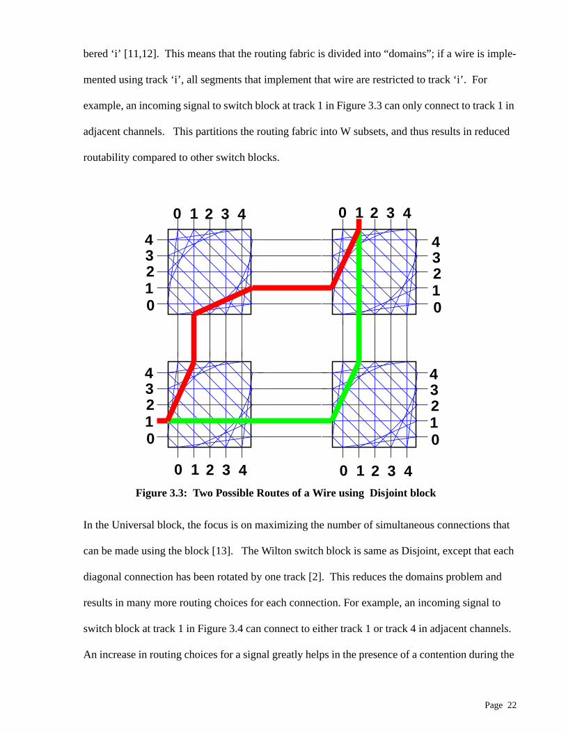
Three switch block architectures have been proposed in previous work: the Disjoint Switch Block
[11,12], the Universal Switch Block [13], and the Wilton Switch Block [2]. The architecture of
each is shown in Figure 3.2, where dotted lines indicate the potential connections which can be
made using the particular switch block.
3.1.1 COMPARISON OF EXISTING SWITCH BLOCKS
In each Switch Block, each incoming track can be connected to three outgoing tracks. The topol-
ogy of each block, however is different. The difference between the blocks is exactly which three
outgoing tracks each incoming track can be connected.
In Disjoint block, the switch pattern is “symmetric”, in that if all the tracks are numbered as
shown in Figure 3.2(a), each track numbered ‘i’ can be connected to any outgoing track also num-
0 1 2 3 4
0 1 2 3 4
0
1
2
3
4
0
1
2
3
4
0 1 2 3 4
4
3
2
1
0
0 1 2 3 4
4
3
2
1
0
0 1 2
0 1 2
2
1
0
2
0
1
3
4
3
4
3 4
3 4
Figure 3.2(a): Disjoint Figure 3.2(b): Universal Figure 3.2(c): Wilton
Page 22
bered ‘i’ [11,12]. This means that the routing fabric is divided into “domains”; if a wire is imple-
mented using track ‘i’, all segments that implement that wire are restricted to track ‘i’. For
example, an incoming signal to switch block at track 1 in Figure 3.3 can only connect to track 1 in
adjacent channels. This partitions the routing fabric into W subsets, and thus results in reduced
routability compared to other switch blocks.
In the Universal block, the focus is on maximizing the number of simultaneous connections that
can be made using the block [13]. The Wilton switch block is same as Disjoint, except that each
diagonal connection has been rotated by one track [2]. This reduces the domains problem and
results in many more routing choices for each connection. For example, an incoming signal to
switch block at track 1 in Figure 3.4 can connect to either track 1 or track 4 in adjacent channels.
An increase in routing choices for a signal greatly helps in the presence of a contention during the
0 1 2 3 40 1 2 3 4
0 1 2 3 4 0 1 2 3 4
01234
01234
01234
01234
Figure 3.3: Two Possible Routes of a Wire using Disjoint block

Page 23
routing process because if track 1 is already being used by another net then the track 4 could be
used (Figure 3.4) to make the required connections. This is no longer true if the Disjoint block is
used (Figure 3.3), and the routing may fail. This makes Wilton switch block more routable than
the Disjoint block.
All the switch blocks require same number of switches to implement, and hence have same area
efficiency for non-segmented FPGA architectures.
3.2 NEED FOR A NEW ARCHITECTURE
The Switch blocks in Section 3.1 were developed and evaluated for FPGA architectures consist-
ing of only single-length wires/tracks i.e non-segmented architectures. Real FPGAs, however,
0 1 2 3 40 1 2 3 4
0 1 2 3 4 0 1 2 3 4
01234
01234
01234
01234
Figure 3.4: Two Possible Routes of a Wire using Wilton

Page 24
typically employ longer segments which connect distant Switch Blocks with less effective capaci-
tive loading resulting into FPGAs with improved speeds. The longer segments have less effective
capacitance because they need to pass through fewer switches compared to short segments, and
the delay of a net increases quadratically with the number of switches that it passes through. This
idea of segmentation was also explained in Chapter 2 of this thesis. In order to take full advantage
of the benefits that segmented architectures have to offer, the design of a new Switch Block most
suitable for segmented architectures is very important. Although all of the existing switch blocks
can be used in segmented architectures, they will not provide the best density or speed; this is due
to their implementation, as described in the next section.
3.2.1 SWITCH BLOCK IMPLEMENTATIONS
The Figure 3.5 shows the implementation of both Disjoint and Wilton switch blocks for an FPGA
architecture which consists of wires that span only one logic block, and hence all tracks terminate
at each switch block.
Each arrow in Figure 3.5 represents a programmable connection, which can be implemented
using a pass transistor or a tri-state buffer (as shown in Figure 3.6). From the Figure 3.5, it is clear
Figure 3.5(a): Disjoint Implementation Figure 3.5(b): Wilton Implementation

Page 25
that each pair of incident track requires 6 switches.
For segmented architectures, on the other hand, the wires/tracks span more than one logic block.
As shown in Figure 3.10, for any given switch block, some tracks terminate at the switch block
while others pass through. For wires that pass through, only 1 switch per track is required if the
Disjoint block is used as shown in Figure 3.7(a). In this case the other 5 switches are redundant.
The Wilton block, however, requires 4 switches for the same track as shown in Figure 3.7(b) [1].
This clearly shows that the Disjoint switch block will have smaller area than the Wilton. How-
ever, as described in Section 3.1.1 the Wilton block has better routability. In the next section, we
present a switch block for segmented architectures which combines the routability of the Wilton
block with the area efficiency of the Disjoint block.
or
Figure 3.6: Two Types of Switches
Figure 3.7a: Disjoint Implementation Figure 3.7b: Wilton Implementation

Page 26
3.3 NEW SWITCH BLOCK
We present a new Switch Block, Imran, which combines the routability of the Wilton block and
the implementation efficiency of the Disjoint block. The Figure 3.8(c) shows the switch block for
W=16 and s=4 (s is the track length).
The main idea is to divide the incoming tracks in a channel into two subsets: (1) the tracks that
terminate at the switch block, and (2) the tracks that do not terminate at the switch block. Those
tracks which do not terminate at the switch block are interconnected using a Disjoint switch pat-
tern as shown in Figure 3.8(a). Due to the symmetry of the Disjoint block only one switch is
required for each incoming track. The tracks which do not terminate at the switch block are inter-
connected using a Wilton switch pattern, as shown in Figure 3.8(b). The two patterns can be over-
layed to produce the final switch block, as shown in Figure 3.8(c). Clearly this pattern can be
extended for any W and ‘s’.
Compared to Wilton switch block the new switch block requires fewer transistors (for wires that
do not terminate), and compared to Disjoint switch block, the new block partitions the routing
into fewer subsets. The Disjoint partitions the routing into W subsets, while the new switch
a) connections for tracks that pass through switch block
b) connections for tracks that end at switch block
c) Sum of a+b: Final Switch Block
Figure 3.8: New Switch Block (W = 16, s = 4)

Page 27
block partitions the routing in ‘s’ subsets. Since there are fewer subsets, each subset is larger, and
thus there are many more choices for each routing segment.
3.4 EXPERIMENTAL METHODOLOGY
In order to compare the proposed switch block to the existing switch blocks, nineteen large bench-
mark circuits were used, and a CAD flow similar to the one shown in Chapter 2 (Figure 2.7) was
employed. Each benchmark circuit was first mapped to 4-LUTs, and flip-flops using FlowMap/
FlowPack [15]. The lookup tables and the flip-flops were packed into BLEs, and BLEs were
packed to logic blocks using VPACK [3]. VPR was then used to place and route the circuit [3].
For each circuit and for each architecture, the minimum number of tracks per channel needed for
100% routability were found using VPR; this number was then multiplied by 1.2, and the routing
was repeated. This “low stress” routing is representative of the routing performed in real industrial
designs. Similar methodology has been used by Betz [1], to evaluate various detailed routing
architecture parameters. First, we describe the area and delays models used by the VPR in Sec-
tion 3.4.1. Next, we describe the FPGA architecture which we used to evaluate the new switch
block in Section 3.4.2. Finally, Section 3.4.3 explains more about our experimental methodology.
3.4.1 AREA AND DELAY MODELS
The area model used by VPR is based on counting the number of minimum-width transistor areas
required to implement each FPGA architecture. A minimum-width transistor area is simply the
layout area occupied by the smallest transistor that can be contacted in a process, plus the mini-
mum spacing to another transistor above it and to its right as shown in Figure 3.9.

Page 28
Since the area of commercial FPGAs is dominated by the transistor area, the most accurate way to
assess the area of an FPGA architecture, short of laying it out, is to estimate the total number of
transistor areas required by its layout. This gives (roughly) a process-independent estimate of an
FPGA architecture area [1]. In addition, VPR uses an Elmore delay [25] model to estimate vari-
ous timing delays.
3.4.2 ARCHITECTURAL ASSUMPTIONS
In our effort to evaluate the new switch block, we assume an Island-Style FPGA segmented
architecture as shown in Figure 3.10. Each logic block is assumed to consist of 4 BLEs (N = 4).
The logic block has 10 inputs (I = 10), and 4 outputs (one output per BLE).
Figure 3.9: Minimum-width transistor area
���������
���������
������
������
������
������
������
������
���������
���������
������
������
Minimum spacing
Diffusion
Contact
Minimum spacing
Poly
dotted reactangle indicates
1 min.-width transistor area

Page 29
The Interconnect Matrix (see Chapter 2) allows any of the logic block inputs (I), or any of the
BLE output to be connected to any of the BLE inputs. A logic block having this connectivity is
referred to as “fully connected” or a “fully populated” logic block. It is also assumed that the 4
flip flops in the logic block are clocked by the same clock, and that this clock is routed on the glo-
bal routing tracks (dedicated tracks). Each of the logic block inputs or the outputs can be con-
nected to one-quarter of the tracks in a neighboring channel (Fc= 0.25W).
Each routing channel consists of W parallel fixed tracks. We assume that all the tracks are of the
same length ‘s’.
If s > 1, then each track passes through s-1 switch blocks before terminating. If s=1, each track
only connects neighboring switch blocks (a non-segmented architecture). A track can be con-
nected to a perpendicular track at each switch block through which the track travels, regardless of
LOGIC BLOCK SWITCH BLOCKROUTING CHANNEL
Figure 3.10: Island-Style Segmented Routing Architecture

Page 30
whether the track terminates at this switch block or not. The start and the end points of the tracks
are staggered, so that not all the tracks start and end at the same switch block. This architecture
was shown to work well in [1,14], and is a more representative of the commercial devices than
the architectures considered in the previous switch block studies [2,12,13]. Figure 3.7 shows this
routing architecture graphically for W = 8, and s = 4. A 0.35µm, 3.3 V CMOS Taiwan Semi-con-
ductor Manufacturing (TSMC) process was used for all of our investigations in this chapter.
3.4.3 FLOATING vs. FIXED NUMBER OF TRACKS
Our methodology consisted of finding the minimum number of tracks per channel needed for
100% routability using VPR for each benchmark circuit and for each architecture. This is differ-
ent than in a normal FPGA CAD flow in which the number of tracks in each channel is fixed, and
the goal is to find any routing which meets timing constraints. To understand our reasoning for
performing experiments in this way, consider the alternative. We could have assumed a fixed
number of tracks per channel, and obtained a “fit/no fit” decision for each benchmark circuit for
each switch block, depending on whether or not the circuit could be completely routed in the
given architecture. The problem with this approach is in the granularity of the measurements.
Using this technique, small improvements in switch block routability would not be evident unless
many (hundreds of) benchmark circuits were used.
Rather than using hundreds of benchmark circuits, we allow the number of tracks per channel to
vary, and find the minimum number of tracks in each channel required to completely route the cir-
cuit. This minimum number is then used as a flexibility measurement (a switch block that results
in fewer tracks in each channel is deemed more routable).

Page 31
This routability is then reflected in the area model by including the area of the routing tracks in the
area estimate of each tile. The motivation here is that a FPGA manufacturer can always compen-
sate for reduced routability by increasing the number of tracks in each channel. Including the
number of tracks in each channel in the area model thus provides a natural way to compare archi-
tectures in terms of both routability and area.
3.5 RESULTS
Figure 3.11 shows the area comparisons for each of the four switch blocks as a function of ‘s’(the
segmentation length). The vertical axis is the number of minimum-width transistor areas per tile
in the routing fabric of the FPGA, averaged over all benchmarks (geometric average). In addition
to the transistors in the routing, the tile also contains one logic block which consists of 1678 min-
imum-width transistor areas [3]. Hence by adding 1678 to each point in the Figure 3.11, entire
area per tile can be obtained.

Page 32
The above graph clearly shows that the new switch block (Imran) performs better than any of the
previous switch blocks over the entire range of segmentation lengths, except for s =1, in which the
new switch block is same as the Wilton block. The best area results are obtained for s = 4; at this
point, the FPGA employing the new switch block requires 13% fewer transistors in the routing
fabric.
The Figure 3.12 shows the delay comparison for each of the four switch blocks. The vertical axis
is the critical path of the each circuit, averaged over all benchmark circuits.
0 2 4 6 8 10 12 14 165000
5500
6000
6500
7000
7500
8000
8500
9000
9500
Segment Length
Are
a o
f R
outin
g
Disjoint UniversalWilton Imran
Figure 3.11: Area Results

Page 33
Clearly the choice of the switch block has little impact on the speed of the circuit, except for the
Wilton block. For
s = 4, the new switch block results in critical paths which are 1.5% longer than in an FPGA
employing the Disjoint switch block. However, this is the average over 19 circuits; in 9 of the 19
circuits, the new switch block actually resulted in faster circuits.
The Figure 3.13 shows the comparison of the channel width required, when each of the switch
block is employed.
0 2 4 6 8 10 12 14 1645
50
55
60
65
70
75
80
Segment Length
Crit
ical
Pat
h (n
s)
Disjoint UniversalWilton Imran
Figure 3.12: Delay Results

Page 34
Clearly the new switch block requires the least number of tracks per channel to route a circuit,
except for Wilton switch block. This is because of the tracks which do not terminate at the switch
block. Those tracks are interconnected using a Disjoint switch pattern in the new switch block
which is less routable than the Wilton block.
3.6 CONCLUSION
We have presented a new switch block, Imran, for FPGAs with segmented routing architectures.
The Imran block combines the routability of the Wilton switch block with the area efficiency of
the Disjoint. We have shown with the experimental results that the new switch block outperforms
all previous switch blocks over a wide range of segmented routing architectures. For a segment
0 2 4 6 8 10 12 14 1625
30
35
40
45
50
55
60
65
70
75
Segment Length
Rou
ting
Tra
cks
To
Rou
te
Disjoint UniversalWilton Imran
Figure 3.13: Channel Width Results

Page 35
length of 4, the Imran switch block results in an FPGA with 13% fewer routing transistors. We
have also shown that the speed performance of the FPGAs employing the new switch block is
roughly the same as that obtained using the previous best switch blocks. Hence the use of Imran
switch block would result in FPGAs with the best area-delay performance.

Page 36
CHAPTER 4
ROUTING WITHIN THE LOGIC BLOCK: THE INTER-CONNECT MATRIX
The routing between the logic blocks and the routing within each logic block are two major fac-
tors determining an FPGA’s speed and the achievable logic density. In the previous chapter, we
investigated a key routing structure for routing between the logic blocks. In this chapter, we
investigate the architecture of the Interconnect Matrix which is one of the key routing structures
within each logic block.
For clustered FPGAs, each logic block consists of more than one BLE. Figure 4.1 shows a logic
block with ‘N’ such BLEs. The Interconnect Matrix shown in the logic block determines all the
possible connections from the logic block inputs ‘I’ to each of N*k BLE inputs. The feedback
paths allow the local connections to be made from within the logic block. In most commercial
FPGAs such as Altera 8K and 10K [19], the Interconnect Matrix is fully connected i.e any of the
logic block inputs ‘I’ can be connected to any of the BLE inputs, and any of the BLE outputs can
be fed back to any of the BLE inputs. In some FPGAs such as Xilinx XC5000, the Interconnect
Matrix is nearly fully connected or depopulated [18,20]. In a depopulated Interconnect Matrix,
only a subset of the logic block inputs, and the feedbacks can be connected to each of N*k BLE
inputs.

Page 37
Clearly, the Interconnect Matrix adds delay to the incoming signal to the logic block, and also
adds delay to each feedback signal. The size of the Interconnect Matrix determines the delay pen-
alty to be added to an incoming or a feedback signal. The Interconnect Matrix is normally imple-
mented using binary tree multiplexers. The number of logic block inputs ‘I’ and the number of
feedback paths determines the size of these multiplexers, and as the logic block size grows the
size of these multiplexers grows very quickly. This adds not only the additional delay, but also a
significant area penalty making FPGAs with large logic block sizes infeasible. Although the
Interconnect Matrix is a very significant routing structure, there has been no published work
investigating its architecture. Thus a study investigating Interconnect Matrix architecture is of
enormous industrial and academic interest and value.
More specifically, the question that we wish to address in the next two chapters is whether the
connectivity provided by a fully connected Interconnect Matrix is more than what is actually
Interconnect
Matrix
k
k
k
BLE #1
BLE #2
BLE #NI N
N-Logic Blockoutputs
Logic Block/Logic Cluster
N feedbacks
I-Logic Blockinputs
Figure 4.1: Logic Block

Page 38
needed. Intuitively, the more flexible the Interconnect Matrix is, the more programmable switches
the matrix will contain. These programmable switches add capacitance and resistance to each
routing track, and consume chip area. Thus, a partially depopulated matrix will likely be faster
and smaller. A smaller matrix will have a secondary effect: a smaller switch matrix leads to a
smaller logic block; this reduces the length of the wires connecting distant switch matrices, mak-
ing these routing wires faster.
On the other hand, reducing the connectivity within each Interconnect Matrix has two potentially
negative effects:
1. Reducing the connectivity makes packing circuit BLEs into logic blocks more difficult. In general, it may be that
a given logic block can not be filled completely, due to interconnection requirements between the BLEs packed
into that logic block. The fewer programmable switches that are in one logic block, the more likely it is that one
or more BLE locations in a logic block will be unused. This may lead to a reduction in logic density.
2. In a fully populated Interconnect Matrix, the input and output pins arefully permutable, in that any pin can be
swapped with any other pin, without affecting the feasibility of the packing solution. This is a feature that a CAD
tool that routes signals between logic blocks can take advantage of. Since the connections between the logic
block pins and the routing tracks outside the logic blocks are not fully populated, it may be that a feasible route
between logic blocks is easier to find if some pins are permutable.
In a partially populated Interconnect Matrix, however, the inputs and output pins may not be
fully permutable. This may lead to a more difficult routing task, which can only be compen-
sated for by including more routing tracks in each channel (leading to reduced logic density).
Thus, whether or not each Interconnect Matrix should be depopulated or fully connected is not

Page 39
clear. In this chapter, we investigate how the depopulation affects the amount of logic that can be
packed into each logic block. A novel packing algorithm has been developed for this task; this
algorithm will also be described in this chapter. In the next chapter, we will take into account the
routing between logic blocks and will investigate how the depopulation affects the overall
routability, speed, and logic density of the FPGA.
4.1 ARCHITECTURAL ASSUMPTIONS
We assumed an island-style segmented FPGA architecture as described in Chapter 3 (Figure 3.10,
Section 3.4.2). A
4-LUT is used as before. The logic block size (N) is varied from 4 to 16. Each routing channel
consists of W parallel fixed tracks. We assume that all the tracks are of the same segment length
‘s’. The segment length ‘s’ was kept constant (s = 4), because our results from Chapter 3 indi-
cated that an FPGA architecture employing 4 to 8 segment length would have best area-delay per-
formance. This is also in conformance with previously published results in [1], investigating the
segmentation length. The buffers driving the segments comprised of a 50% pass transistors, and
50% tri-state drivers. The new switch block presented in Chapter 3, Imran, was used. It has been
shown that the best area-efficiency for Wilton switch block occurs when each of the logic block
inputs or the outputs can be connected to one-quarter of the tracks in a neighboring channel (Fc=
0.25 x W), and Disjoint switch block when Fc = 0.5 x W [1]. Since we used the new switch block
Imran, which is a combination of both Wilton and Disjoint, we used an
Fc = 0.5 x W. Betz [1] showed that an I=2N+2 (for N less than or equal to 16 and k = 4) is suffi-
cient for good logic utilization. Hence we use an I = 2N + 2 for each of the architecture that we
will investigate. A 0.25µm, 2.5 V TSMC process was used for our investigations in this Chapter,

Page 40
and a CAD flow similar to the one presented in Chapter 2 (Figure 2.7) was employed.
4.2 METHODOLOGY
In order to determine the suitable connectivity that should be provided by the Interconnect Matrix,
we need to investigate how connectivity defined by the Interconnect Matrix affects the amount of
logic that can be packed into each logic block. All available packing tools can only target an
FPGA with fully connected Interconnect Matrix. Therefore, we developed a new packing tool, D-
TVPACK, which is an enhancement of an existing algorithm.
4.3 PACKING
The packing consists of taking a netlist of Look Up Tables (LUTs) and latches, and producing a
netlist of logic blocks, where a logic block may comprise of one or more Basic Logic Elements
(BLEs). The main objectives of the packing process are twofold: (1) Combining the LUTs and the
latches into BLEs, and (2) Grouping the BLEs into logic blocks. Therefore any packing algo-
rithm must meet the following four constraints:
(i). The number of BLEs in each logic block must be less than or equal to the logic block size N.
(ii). The number of distinct input signals generated outside the logic block must be less than or
equal to the total
number of logic block inputs.
(iii). The number of different clocks used by the BLEs must be less than or equal to the total num-
ber of clock inputs
to the logic block.

Page 41
(iv). The total number of logic blocks in the final netlist should be as small as possible.
In addition to meeting above basic constraints a good packing algorithm should also try to find a
packing solution such that the least number of signals need to be routed between the logic blocks.
This makes it easier for a router to route the required signals, and results in better performing
FPGAs.
4.3.1 OVERVIEW OF EXISTING PACKING TOOL: T-VPACK
T-VPACK is an existing algorithm to perform this packing [8]. It first combines LUTs and latches
into BLEs, and then groups these BLEs into logic blocks. It greedily packs BLEs into logic
blocks until there is no BLE which is left unclustered (not assigned to a logic block). This greedy
packing process begins by choosing and placing a seed BLE in a logic block. Next, T-VPACK
selects a BLE with the highestAttraction (defined below) to the current cluster which could
legally (satisfies all the cluster constraints mentioned above) be added to the current logic block,
and adds it to the cluster. This addition of the BLEs to a cluster continues until the logic block is
either full, or no BLE is left which could be legally added to the current logic block. Then a new
seed BLE is placed in a new logic block, which is filled as before. This process continues until all
the BLEs have been assigned to a logic cluster/logic block. TheAttraction between a BLE and
the current cluster is defined as the weighted sum of the number of nets connecting the BLE and
the cluster being filled, and the gain in the critical path delay ( Criticality(B) ) that would be
obtained, if the BLE is packed into the cluster [8].
In the above equation, the B denotes an unclustered BLE, and C denotes the current logic block.
The G is a normalization factor, andα is a trade-off variable which determines the dependence of
Attraction B( ) α Criticality B( )× 1 α–( ) Nets B( ) Nets C( )∩G
--------------------------------------------------×+=

Page 42
algorithm on either critical path or pin sharing.
4.3.2 THE NEW PACKING TOOL: D-TVPACK
The new packing tool D-TVPACK is an extension of the above algorithm that supports depopu-
lated Interconnect Matrix architectures. A depopulated Interconnect Matrix has less connectivity
as compared to a fully connected matrix. All the BLEs within a logic block are interchangeable
in a fully connected matrix, while they are not interchangeable if the matrix is depopulated. This
is the key difference between a fully connected and a depopulated matrix. In fully connected
matrix, all the cluster inputs ‘I’ are equivalent, and hence a router can route all the incoming sig-
nals to the logic block by connecting them to any of the cluster inputs ‘I’. In a depopulated
matrix this is no longer true, and a router can not treat all the logic block inputs ‘I’ equivalent.
This specifies an additional constraint that a packing algorithm must also take into account. This
constraint dictates that the packing tool must assign a specific location to any BLE that it places in
a logic block, and it must assign a specific logic block input pin to each input nets. The output
net of the BLE is assigned to the logic block output pin for the location. The pseudo-code for the
complete algorithm is given below.
PSEUDO-CODE: D-TVPACK
main (){ while ( no BLE left unclustered ) { for a new cluster Select an unclustered seed BLE --all seeds are legal Assign seed BLE to least connectivity location Assign seed BLE input nets to the cluster inputs ‘I’
while ( cluster empty )

Page 43
{ A = highest_suitable_ble(); if (A == FALSE) break; else Assign the BLE to the suitable found location in the current cluster } }
return;}
boolean highest_suitable_ble(void){ for all legal unclustered BLEs --in the order of theirAttraction { --highest attraction first Z = ble_fit_for_cluster (BLE); if ( Z == TRUE ) return TRUE; else continue; }
return FALSE;}
boolean ble_fit_for_cluster (BLE){ DONE = FALSE; for all the available locations in the cluster --in the order of their connectivity { --least connectivity first K = output_net _can_be_assigned_to_this_location;
if (K == FALSE) continue; else DONE = TRUE;
if (DONE == TRUE) { C = input_nets_can_be assigned_to_this_location; --tries all possible permu-tations --nets assigned to pins ‘I’ in order of theirconnectivity --maximum connection pins are assigned anet first if (C == FALSE) DONE = FALSE; else break; } }
return DONE;}

Page 44
Like T-VPACK, D-TVPACK also employs a greedy packing strategy. The algorithm proceeds by
selecting a legal (meets the basic packing constraints for a cluster) seed BLE and assigns it to a
least connectivity location in a cluster. Theconnectivity of a location in the cluster is defined as
the number of connections that can be made from the logic block inputs ‘I’ to the BLE location in
the cluster (Figure 4.2 shows a logic block with two BLE locations having connectivity 1 and 2).
The seed BLE input nets are then assigned to the logic block inputs ‘I’. Of all the logic block
inputs ‘I’, the assignment of the nets is made first to those pins which have the maximum connec-
tivity. Theconnectivity of the logic block pin is defined as the number of BLE inputs that a logic
block input pin can be connected to (Figure 4.2 shows a logic block with two input pins having
connectivity 1 and 2). The rationale for this selection can be seen by looking at theAttraction
equation. The BLEs with most connections to the current cluster (being filled) are likely to be
chosen to place in the cluster. Therefore, available BLE locations within a logic block with most
connectivity, and the used logic block input pins with most connectivity would greatly help in
assigning future BLEs to this cluster.
Connectivity oflogic block pin
Logic Block
Connectivity of
1
Connectivity of
this location = 2
this location = 1
2
Figure 4.2: Connectivity Example

Page 45
The addition of the BLEs to a cluster continues until the logic block is either full, or there is no
BLE left which could be legally added to the current logic block, or there are legal BLEs, but not
enough connectivity left in the logic block to assign them to a location in the cluster being filled.
Then, a new seed BLE is placed in a new logic block, which is filled as before. This process con-
tinues until there is no BLE left to cluster. It is important to note that the seed BLE must fit some
location in a logic block. This ensures that all the BLEs are clusterable (can be assigned to a clus-
ter), and hence specifies a constraint on the minimum connectivity required from an Interconnect
Matrix.
In the original T-VPACK algorithm, each incoming net to a logic block is assigned to only one
logic block input pin, because due to full connectivity in the Interconnect Matrix, there would be
no need to assign the same net to more than one input pin. With a depopulated Interconnect
Matrix, however, this is no longer true; a net assigned to a particular input pin may not be able to
connect to every BLE input in the cluster. Yet, in our algorithm, we make the same restriction as
in T-VPACK that no incoming net is assigned to more than one logic block input pin. This con-
straint may result in the rejection of a high attraction BLE for a logic block, and hence may reduce
the achievable packing density. We have not quantified this effect, however, we feel that the over-
all impact on the achievable packing density will be very small.
4.4 EXPERIMENTAL EVALUATION
In this section, we evaluate the effect of a particular class of depopulated architectures on the
achievable logic density using the proposed packing algorithm, D-TVPACK.

Page 46
It is important to note that the packing results significantly impact the overall performance of an
FPGA. A good packing solution is expected to pack the BLEs in a given circuit into the least
number of the logic blocks, and also reduce the number of the connections between the logic
blocks so that the routing can be minimized resulting into faster and more efficient implementa-
tions. In order to describe the effect of reducing the connectivity of the Interconnect Matrix, we
use several packing statistics such as Logic Utilization, Logic Block Input Utilization, Number of
Logic Block Outputs used outside the Logic Block, and the total Number of logic blocks after
packing process. These metrics give us insight into how the number of logic blocks changes with
the connectivity, and how the connectivity affects the number of connections which need to be
routed between the logic blocks. We used 23 large Microelectronics Corporation of North Caro-
lina (MCNC) benchmark circuits for our investigations.
4.4.1 DEPOPULATION PATTERNS CONSIDERED
The Figure 4.3 shows the Interconnect Matrix patterns which we used for our investigations. The
notation ‘A/B’ (% of total BLE inputs in a cluster that a cluster input pin can be connected to / %
of total BLE inputs in a cluster that a cluster output pin can be connected to) is used to refer to
each pattern given below. For example, a 50/100 partially depopulated architecture refers to a
partially depopulated architecture in which each Interconnect Matrix in a logic block allows any
of the cluster inputs ‘I’ to connect to only 50% of the total BLE inputs in the logic block. Thus, a
fully connected architecture can also be referred to as 100/100 (any cluster input ‘I’ can connect
to any of the BLE inputs and any cluster output can feedback to any of the BLE inputs).

Page 47
4.4.2 LOGIC UTILIZATION
The Figure 4.4 shows how the logic utilization varies with the cluster size N. The horizontal axis
shows the cluster size N. The vertical axis shows the Logic Utilization (averaged over 23 bench-
marks). The ‘Logic Utilization’ is defined as the average number of BLEs per logic block that a
circuit is able to use divided by the total number of BLEs per cluster (N).
I Cluster Inputs N Feedbacks
4N
BL
E In
pu
ts
I Cluster Inputs N Feedbacks
4N
BL
E In
pu
ts
I Cluster Inputs N Feedbacks
4N
BL
E In
pu
ts
I Cluster Inputs N Feedbacks
4N
BL
E In
pu
ts
I Cluster Inputs N Feedbacks
4N
BL
E In
pu
ts
I Cluster Inputs N Feedbacks
4N
BL
E In
pu
ts
(a): 100/100 (b): 50/100 (c): 25/100
(d): 100/50 (e): 50/50 (f): 25/25
Figure 4.3: Interconnect Matrix Patterns

Page 48
From the figure, it is quite clear that the type of Interconnect Matrix architecture has very little
effect on the Logic Utilization. The 100/100, 50/100, 100/50, 50/50 architectures have almost the
same logic utilization. The logic utilizations of the 25/100 and 25/25 architectures, however, vary
slightly from the others. It may seem that 50/100 architecture has better Logic Utilization, but
one should not reach to a conclusion about the packing results without looking at other important
metrics given in the following sections to compare various architectures.
4.4.3 NUMBER OF LOGIC BLOCKS
The Figure 4.5 shows how the number of logic blocks varies with the cluster size (N) for the vari-
ous Interconnect Matrix architectures. The horizontal axis shows the cluster size N. The vertical
axis shows the normalized number of logic blocks that the packing tool used, in order to pack all
4 6 8 10 12 14 160.955
0.96
0.965
0.97
0.975
0.98
0.985
0.99
0.995
1
Cluster Size (N)
Logi
c U
tiliz
atio
n
100/10050/100 25/100 100/50 50/50 25/25
Figure 4.4: Logic Utilization
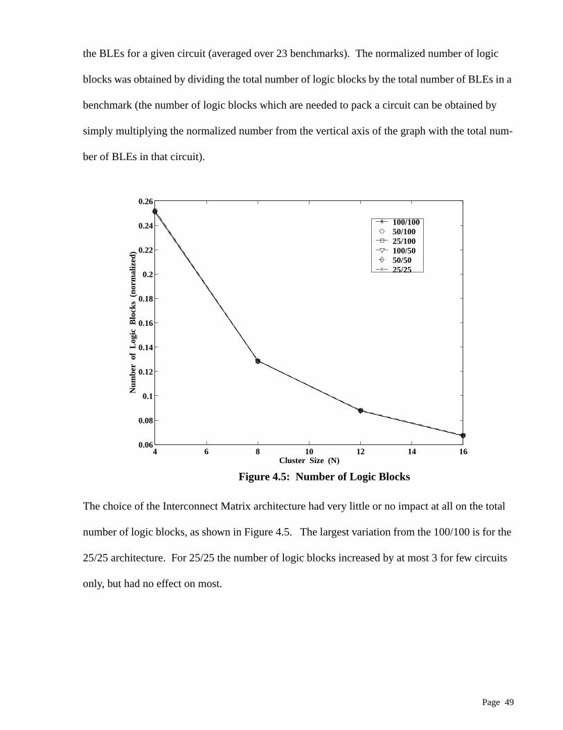
Page 49
the BLEs for a given circuit (averaged over 23 benchmarks). The normalized number of logic
blocks was obtained by dividing the total number of logic blocks by the total number of BLEs in a
benchmark (the number of logic blocks which are needed to pack a circuit can be obtained by
simply multiplying the normalized number from the vertical axis of the graph with the total num-
ber of BLEs in that circuit).
The choice of the Interconnect Matrix architecture had very little or no impact at all on the total
number of logic blocks, as shown in Figure 4.5. The largest variation from the 100/100 is for the
25/25 architecture. For 25/25 the number of logic blocks increased by at most 3 for few circuits
only, but had no effect on most.
4 6 8 10 12 14 160.06
0.08
0.1
0.12
0.14
0.16
0.18
0.2
0.22
0.24
0.26
Cluster Size (N)
Num
ber
of
Logi
c B
lock
s (
norm
aliz
ed)
100/10050/100 25/100 100/50 50/50 25/25
Figure 4.5: Number of Logic Blocks

Page 50
4.4.4 LOGIC BLOCK OUTPUTS USED OUTSIDE THE LOGIC BLOCK
The Figure 4.6 shows how the logic block outputs used outside the logic block changes with the
cluster size (N) for the various Interconnect Matrix architectures. The horizontal axis shows the
cluster size N. The vertical axis shows the average number of logic block outputs used outside a
logic block (divided by N, and averaged over 23 benchmarks).
The 100/100 and the 50/100 had almost the same number of outputs used outside the logic block,
however, it decreased for 25/100, and increased for others.
4.4.5 LOGIC BLOCK INPUT UTILIZATION
The Figure 4.7 shows how the logic block input utilization changes with the cluster size N. The
4 6 8 10 12 14 16
0.65
0.7
0.75
0.8
Cluster Size (N)
Logi
c B
lock
Out
puts
Use
d O
utsi
de L
ogic
Blo
ck (
norm
aliz
ed)
100/10050/100 25/100 100/50 50/50 25/25
Figure 4.6: Logic Block Outputs Used Outside the Logic Block

Page 51
horizontal axis shows the cluster size N. The vertical axis shows the logic block inputs utilization
(averaged over 23 benchmarks). The logic block input utilization is defined as the average num-
ber of logic block inputs that a circuit is able to use divided by the total number of cluster inputs
‘I’.
The input utilization changes slightly for 100/100, 50/100, 25/100, 100/50 and 50/50. The largest
variation from 100/100 is for 25/25 architecture. For less flexible architectures such as 25/25, the
Logic Block Input Utilization increased. This is due to less sharing within the cluster and is in
consistent with the behavior in Figure 4.6, where the number of outputs used outside a logic block
also increased for less flexible architectures.
Various conclusions can be drawn from the results presented in Figures 4.4, 4.5, 4.6 and 4.7. The
4 6 8 10 12 14 160.46
0.48
0.5
0.52
0.54
0.56
0.58
0.6
0.62
0.64
0.66
Cluster Size (N)
Logi
c B
lock
Inp
uts
Util
izat
ion
100/10050/100 25/100 100/50 50/50 25/25
Figure 4.7: Logic Block Input Utilization

Page 52
most significant observation is that the 100/100 and 50/100 architectures produced almost identi-
cal packing results, however, the packing did change slightly for other architectures.
4.5 CONCLUSION
In this chapter we focused our attention to the architecture of an Interconnect Matrix. We first
presented a new packing tool D-TVPACK which is capable of targeting an FPGA with virtually
any Interconnect Matrix. We investigated the effects of the Interconnect Matrix connectivity by
comparing various packing statistics. This enabled us to answer the question that we earlier posed
in the start of this chapter that whether the connectivity provided by a fully connected Intercon-
nected Matrix is more than what is needed. Indeed, we have shown that the connectivity provided
by a fully connected matrix is more than is required. We investigated various architectures such
as 100/100, 50/100, 25/100, 100/50, 50/50, and 25/100. We showed that 100/100 and 50/100 pro-
duced almost identical packing results, however the packing results did change slightly for the
other architectures. This clearly suggests that the connectivity of the Interconnect Matrix may be
reduced, which may result into denser and faster FPGAs. In the next chapter, we investigate the
implications that this reduction in connectivity has on the overall speed and area performance of
an FPGA.

Page 53
CHAPTER 5
IMPLICATIONS OF REDUCED CONNECTIVITY OFINTERCONNECT MATRIX
In the previous chapter, we investigated the connectivity of Interconnect Matrix and suggested
that the Interconnect Matrix’s connectivity may be reduced. In this chapter, we will investigate
the implications that this reduction in the connectivity of the Interconnect Matrix may have on the
overall speed and the area performance of an FPGA.
There are two factors which determine an FPGA architecture’s performance: (1) the FPGA’s tran-
sistor-level architecture, and (2) the quality of the results produced by its CAD tools (a complete
CAD flow for FPGAs is shown in Chapter 2, Figure 2.7). In order to evaluate any low level
architectural features such as the connectivity of an Interconnect Matrix, it is absolutely critical to
determine what implications this may have on the quality of the results produced by the associ-
ated CAD tools and algorithms.
The connectivity of the Interconnect Matrix has significant impact on both the transistor level
architecture and the quality of the results produced by the CAD tools. Therefore, to evaluate
depopulated architectures and to quantify the effect that the depopulation of Interconnect Matrix
has on the overall performance of an FPGA, first we look at how the connectivity of the Intercon-

Page 54
nect Matrix affects the area required to implement a logic block in an architecture, and the various
delays which are associated with different paths through the logic block. Finally, we investigate
the effects of reduced connectivity Interconnect Matrix architectures on the overall performance
of an FPGA, by placing and routing the benchmark circuits using an existing experimental FPGA
place and route tool, VPR.
5.1 AREA OF LOGIC BLOCK
The minimum-width transistor area model described in the Chapter 3 was used to obtain the area
estimates listed in Table 5.1 for a logic block. The Table 5.1 shows the minimum-width transistor
areas required to implement a fully, or depopulated architecture logic block for various cluster
sizes, N. The implementation of a logic block which we used for our investigations is shown in
Figure 5.1 (the figure shows only part of the complete logic block).
Table 5.2 lists the percent savings in logic block area which may be obtained by a 50/100, or
25/100, or 100/50, or 50/50, or 25/25 architecture over a 100/100 architecture.
N 100/100 50/100 25/100 100/50 50/50 25/25
4 1755 1412 1217 1617 1317 1045
8 4965 3759 3106 4662 3435 2561
12 9560 6973 5602 8908 6288 4487
16 15510 11024 8675 14377 9848 6792
Table 5.1: Area of Logic Block for Various Architectures (in min. width transistor areas)

Page 55
A few important observation can be made from the Table 5.2: (1) the Interconnect Matrix has sig-
nificant impact on the area required by a logic block, and logic area savings may range anywhere
from 4.8% to 56.2%, (2) the most significant area gains are obtained by reducing the connectivity
of the cluster inputs, and the connectivity of the feedbacks had very little impact on the logic
area. These observations have important implications when it comes to place and route a circuit
for depopulated architectures.
The 100/100 and 50/100 were shown (in Chapter 4) to produce identical packing results, and
hence from now on we will focus our attention to comparing the overall performance of an FPGA
with these two architectures.
5.2 LOGIC BLOCK DELAYS
The delays of the various paths through the logic block were determined using HSPICE simula-
tions. Using a 0.25µm, 2.5 V TSMC process, a complete netlist of the logic block shown in Fig-
ure 5.1 was developed. The sizing of the buffers and the transistors was done appropriately and
the various delays shown in Figure 5.1 were determined with the actual loads in place.
N 50/100 25/100 100/50 50/50 25/25
4 19.5% 30.7% 4.8% 25.0% 40.5%
8 24.3% 37.4% 6.1% 30.8% 48.4%
12 27.1% 41.4% 6.8% 34.2% 53.1%
16 28.9% 44.1% 7.3% 36.5% 56.2%
Table 5.2: Logic Area Savings of Depopulated Architectures over a 100/100
Architecture.

Page 56
Only 1 of N BLEs and logic block outputs are shown in Figure 5.1. The Interconnect Matrix is
implemented using binary tree multiplexers. Figure 5.1 shows only 2 of N*k input multiplexers
implementing Interconnect Matrix.
Table 5.3 lists the delays for the 100/100 and 50/100 architectures. Although we measured all
timing parameters shown in Figure 5.1, we only present the measurement for
T_clb_ipin_to_sblk_ipin andT_sblk_opin_to_sblk_ipin , since these are the only parameters
that depend significantly on the Interconnect Matrix architecture. Table 5.3 also lists the percent
improvement for the depopulated architectures over a 100/100 architecture.
SRAM
LUT
CLK
Flip
Flop
T_sblk_opin_to_sblk_ipin
T_sblk_opin_to_clb_opin
Logic Block OutputI-Logic Block
inputs
T_clb_ipin_to_sblk_ipin T_comb
T_seq_outT_seq_in
Interconnect Matrix
BLE
Figure 5.1: Logic Block Implementation

Page 57
TheT_clb_ipin_to_sblk_ipin represents the time that it takes an incoming signal (to a logic
block) to go from the input of a logic block to the input of a BLE. The
T_sblk_opin_to_sblk_ipin represents the time that it takes for a feedback signal to go from the
BLE output to the same or the other BLE inputs in the same logic block. From the table, it is clear
that significant (20 to 34%) speed improvements can be obtained by a 50/100 architecture over a
100/100 architecture for an incoming signal to a logic block, however, no significant speed gains
are obtained for the feedback signals. No significant speed gains were obtained for a feedback
signal because each logic block output is loaded by the same number of Interconnect Matrix mul-
tiplexers for both 100/100 and 50/100 architectures. Some speed improvements are observed for
the feedback signals, however. This is due to the smaller size of the multiplexers implementing
the Interconnect Matrix for 50/100 architecture.
5.3 EFFECT OF REDUCED CONNECTIVITY ON THE OVERALL FPGA
PERFORMANCE
In order to evaluate the overall performance of an FPGA architecture, it is critical to evaluate the
impact of the choices made at the transistor level architecture on the quality of results produced
N T_clb_ipin_to_sblk_ipin 100/100 50/100 (ps)
%Savings(50/100 vs100/100)
T_sblk_opin_to_sblk_ipin 100/100 50/100 (ps)
%Savings(50/100 vs100/100)
4 598.6 462.3 22.8% 576.4 574.5 0.3%
8 879.8 698.2 20.6% 852.2 847.0 0.6%
12 1219.0 799.7 34.4% 1188.0 1035.0 12.9%
16 1388.0 984.6 29.1% 1355.0 1355.0 0%
Table 5.3: Selected Logic Block Delays for 100/100 and 50/100 Architectures.

Page 58
by the CAD tools. In the previous section, from the circuit’s design perspective, we have shown
that an FPGA with depopulated Interconnect Matrix will have excellent area-delay performance.
However, how depopulation affects the quality of the results produced by the CAD tools and it’s
effects on the overall FPGA performance is the subject of this section.
The connectivity of the Interconnect Matrix mainly affects two CAD processes: (1) the packing
and, (2) the routing. We thoroughly investigated the effect of depopulation on packing in Chapter
4, and have shown that the depopulation has no or very little effect on the packing process. Now
we investigate how does the depopulation affects the place and route, and thus the overall perfor-
mance.
5.3.1 PLACE AND ROUTE OF LOGIC BLOCKS USING VPR
The Versatile Place and Route (VPR) tool was developed by Betz [3] for FPGA architecture
research. It has been shown to work quite well compared to all other place and route tools.
Therefore, we used VPR to place and route the netlist of logic blocks obtained from the D-
TVPACK.
The routing solution found by the VPR depends on the resistance (R), and the capacitance (C) of
the segment which is given to it. These parameters are used by the timing-driven router to esti-
mate the delays of potential routes, and to guide the router to find solutions which minimize the
overall delays of the final circuit implementation. However, the evaluation of R and C depends on
the number of tracks per channel, which is a dependent variable in our experiments; the number of
tracks required in each channel is not known until after the place and route is complete. There-

Page 59
fore, we used three runs of VPR for each benchmark circuit and for each architecture. For the first
run, some nominal R and C values were chosen for place and route. For the second run, the R
and C values were calculated from the results of the first run. The R and C of the segment was
determined by first finding the length of a tile (square root of the tile area, assuming a square tile),
and using the process dependent parameters (sheet resistance and capacitance per micron) to
determine the overall R and C per segment. Finally, for the third run, R and C values from the
second run were used. The minimum routing area of the last two runs and the associated timing
were used to compare the two architectures. This procedure ensured that accurate results are
obtained for the comparison.
5.3.2 PLACE AND ROUTE RESULTS
Table 5.4 shows the average (over 23 benchmarks) of the routing Area and the area per tile for the
two architectures over a range of cluster sizes (N), and compares a 100/100 architecture with a
50/100 architecture.
The routing area (which includes only routing outside the logic block) increased by between
13.86% and 18.8% due to the reduced routability of the 50/100 architecture. The routability of
NRouting Area
100/100 50/100
%Penalty(50/100 vs100/100)
Area per Tile 100/100 50/100
%Savings(50/100 vs100/100)
4 4656.77 5301.67 13.8% 6412.21 6714.55 - 4.7%
8 8660.21 9972.57 15.2% 13625.4 13732.0 - 0.8%
12 13472.1 15713.2 16.6% 23032.8 22686.5 + 1.5%
16 18205.0 21633.8 18.8% 33715.9 32658.1 + 3.1%
Table 5.4: Routing and Tile Area for a 100/100 and 50/100 Architectures.

Page 60
the 50/100 architecture is reduced because the reduction in the connectivity of the Interconnect
Matrix resulted in a reduction in the permutability of the logic block inputs. This makes it more
difficult for the router to use the global routing tracks effectively, meaning, on average, it uses
more of these tracks to route a given circuit. The area per tile, which is the sum of the logic area
and the routing area did not increase by much for cluster sizes 4 and 8. The area per tile required
by the 50/100 architecture decreased for cluster sizes 12 and 16. This is because the savings in
logic area are more significant in larger logic blocks compared to an increase in the routing area
due to the reduced routability in depopulated architectures.
Table 5.5 shows the minimum channel width required by each of the architecture for various clus-
ter sizes (N), and compares a 100/100 architecture with a 50/100 architecture.
Clearly, the reduction in routability resulted in an increase in the number of tracks required in a
channel by between 16.7% and 19.3%.
Table 5.6 shows the critical path delay for each of the architecture (averaged over 23 bench-
marks), and compares 100/100 architecture with a 50/100 architecture. It is clear from this table
that the overall speed of an FPGA degrades due to depopulation.
NChannel Width
100/100 50/100
%Penalty(50/100 vs100/100)
4 30 35 16.7%
8 41 48 17.1%
12 51 60 17.6%
16 57 68 19.3%
Table 5.5: Channel Width assuming 100/100 and 50/100 Architecture.

Page 61
5.3.3 OTHER DEPOPULATED ARCHITECTURES
In this section, we also compare 100/100 architecture to three other architectures (25/100, 50/50,
25/25) for the cluster size 12.
Table 5.7 shows the delays through the logic block for various depopulated architectures.
Clearly, the depopulated architectures offer significant improvements in logic block delays over a
100/100 architecture.
Table 5.8 shows the routing area, area per tile, channel width, and the critical path delay for vari-
ous depopulated architectures. The table also presents a comparison of depopulated architectures
with a 100/100 architecture.
NCritical Path Delay (ns)
100/100 50/100
%Savings(50/100 vs100/100)
4 192.136 217.682 - 13.3%
8 258.44 253.94 + 1.74%
12 294.175 309.592 - 5.2%
16 349.86 384.489 - 9.9%
Table 5.6: Delay Results for a 100/100 and 50/100 Architecture.
Parameter 100/100 25/100 %Savings 50/50 %Savings 25/25 %Savings
T_clb_ipin_to_sblk_ipin (ps) 1219.0 537.1 55.9% 799.7 34.4% 469.0 61.5%
T_sblk_opin_to_sblk_ipin (ps) 1188.0 1035.0 12.9% 781.6 34.2% 444.4 62.6%
Table 5.7: Delays through the Logic Block for Cluster Size 12, and Percent Savings
obtained by depopulated architectures over a 100/100 architecture.

Page 62
Table 5.8 shows that, by depopulation the routing area increases significantly. This offsets any
logic area gains, and thus the tile area remains the same. In addition, the critical path delay for
depopulated architectures increased significantly. Therefore, from all the results presented in this
section, it is quite clear that the 100/100 (fully connected) architecture offers the best area-delay
performance.
5.4 CONCLUSION
In this chapter, we quantified the advantages and the disadvantages of depopulated architectures.
We have shown that
a large portion of the logic block area is devoted to the Interconnect Matrix. Thus, by depopulat-
ing an Interconnect Matrix 19.5% to 56.2% of the logic block area can be saved. In addition, by
depopulating the delay for a signal going through the logic block can be improved by as much as
35%. However, these improvements and advantages come at the expense of a reduction in the
routability between the logic blocks. This reduction in the routability between the logic blocks
results in a significant increase in the routing area. This increase in routing area offsets any logic
Parameter 100/100 25/100 %Savings 50/50 %Savings 25/25 %Savings
Routing Area 13472.1 16126.0 - 19.7% 16957.6 - 25.9% 19060.3 - 41.5%
Area per Tile 23032.8 21728.6 + 5.7% 23246.2 - 0.9% 23547.3 - 2.2%
Channel Width 51 61 - 19.6% 65 - 27.5% 73 - 43.1%
Critical Delay (ns) 294.175 340.764 - 15.8% 336.431 - 14.4% 382.85 - 30.1%
Table 5.8: Place and Route Results for Cluster Size 12, and Comparison of depopulated
architectures with a 100/100 architecture.

Page 63
area gains, and the area per tile remains approximately the same. Hence, we have shown that the
depopulation degrades the overall performance of an FPGA.

Page 64
CHAPTER 6
CONCLUSIONS AND FUTURE WORK
In this thesis, we investigated critical FPGA routing architecture structures. First, we focused on
one of the key routing structure between the logic blocks: the Switch Block. Next we focused on
one of the key routing structure within each logic block: the Interconnect Matrix.
A switch block is a very important routing structure. The switch blocks define all the possible
connections between the tracks in various channels, and are key to the overall routing flexibility.
The existing switch block architectures have been studied well for non-segmented FPGAs, how-
ever, there has been no work done on the design of the switch blocks most suitable for segmented
FPGAs. We proposed a new switch block structure, Imran, for segmented FPGAs. We have
shown that the new switch block requires 13% fewer transistors in routing, thus FPGAs employ-
ing the new switch block would be most area efficient, and offer the greatest achievable logic den-
sity.
The Interconnect Matrix is a key routing structure within each logic block. It defines all the pos-
sible connections which can be made within each logic block, and is a key to routing flexibility
within the logic block. Most commercial FPGAs employ fully connected Interconnect Matrix
architectures. Some FPGAs also employ depopulated Interconnect Matrix architectures. Both

Page 65
the fully connected and the depopulated architectures have been in commercial use, but there is
very little or no published work investigating the effect of the connectivity on the overall FPGA
performance. By using a realistic FPGA architecture and an experimental approach we thor-
oughly addressed this issue.
Most packing tools which are available for FPGA research can only target FPGAs with fully con-
nected Interconnect Matrix architectures. We presented a new packing algorithm, D-TVPACK,
which is capable of targeting an FPGA with virtually any Interconnect Matrix pattern. Using the
new packing tool, we investigated six Interconnect Matrix architectures (100/100, 50/100, 25/100,
100/50, 50/50, 25/25). We have shown that 100/100 and 50/100 architectures produced almost
identical packing results. Other architectures were very close. This clearly proved that the con-
nectivity of the Interconnect Matrix available in commercial FPGAs (mostly fully connected) is
more than is required.
We thoroughly investigated the effects of reducing the connectivity of the Interconnect Matrix,
and quantified the advantages and the disadvantages of depopulated architectures. We have
shown that significant area and speed gains can be obtained by the depopulated architectures.
These significant gains come at the expense of greater constraint on the routing between the logic
blocks. The constraints on the routing significantly degrades the overall performance of an
FPGA. Therefore, with current routing algorithms, a fully connected architecture offers best area-
delay performance.

Page 66
6.1 FUTURE WORK
There were several FPGA routing architecture issues addressed in this thesis. Each issue brings
up many interesting unanswered questions, where much more research is needed.
We have presented a new and an innovative solution to the switch blocks for segmented FPGAs
problem haunting FPGA architects, but whether it is an optimal solution or not was not shown. In
fact, this work on the switch blocks has stimulated a renewed interest in developing more and
more efficient switch block architectures which are more suitable for complex commercial FPGA
architectures.
In the original T-VPACK algorithm, each incoming net to a logic block is assigned to only one
logic block input pin, because due to full connectivity in the Interconnect Matrix, there would be
no need to assign the same net to more than one input pin. With a depopulated Interconnect
Matrix, however, this is no longer true; a net assigned to a particular input pin may not be able to
connect to every BLE input in the cluster. Yet, in our algorithm, we make the same restriction as
in T-VPACK that no incoming net is assigned to more than one logic block input pin. This con-
straint may result in the rejection of a high attraction BLE for a logic block, and hence may reduce
the achievable packing density. We have not quantified this effect.
The depopulated Interconnect Matrix architectures investigated in this thesis were homogeneous,
where all the BLEs had same amount of connectivity in the logic block, and we did not investigate
any heterogeneous Interconnect Matrix architectures, where BLEs in a logic block may have dif-
ferent amount of connectivity. Although D-TVPACK
is capable of packing BLEs into logic blocks with either homogeneous or heterogeneous Intercon-

Page 67
nect Matrix architectures, the VPR is only able to place and route logic blocks with homogeneous
architectures. Therefore, a new place and route tool is needed to investigate the FPGA architec-
tures with heterogeneous Interconnect Matrix architecture logic blocks.
The only reason, we have shown that the fully connected architecture is the best is due to its rout-
ing flexibility between the logic blocks. But the advantages of the depopulated architectures are
also quite encouraging. The logic area improvement (as much as 56%), and the speed improve-
ment through the logic block (as much as 34%) are quite significant. This prompts the need for
routing algorithms which can better take into account the reduction of routing flexibility due to
depopulation. If an efficient routing algorithm is found, then perhaps depopulating the Intercon-
nect Matrix would be very beneficial.
6.2 SUMMARY OF CONTRIBUTIONS
Three were three major contributions of our work:
• A novel switch block structure, Imran.
• A novel packing algorithm, D-TVPACK, which is capable of targeting FPGAs with either
homogeneous, or heterogeneous Interconnect Matrix architecture logic blocks.
• Quantified the advantages and disadvantages of the depopulated FPGA architectures.
Most important of all, this work has greatly enhanced an understanding of key FPGA routing
architecture structures.

Page 68
REFERENCES
1. Vaughn Betz, “Architecture and CAD for Speed and Area Optimization of FPGAs,” Phd the-
sis, University of Toronto, 1998.
2. Steven J. E. Wilton, “Architecture and Algorithms for Field Programmable Gate Arrays with
Embedded Memory,” Phd thesis, University of Toronto, 1997.
3. Vaughn Betz, Jonathan Rose, “VPR: A New Packing, Placement and Routing Tool for FPGA
Research,” Seventh International Workshop on Field-Programmable Logic and Applications,
1997, pp. 213-222.
4. J. Rose, R.J. Francis, D. Lewis, and P.Chow, “Architecture of Field-Programmable Gate
Arrays: The Effect of Logic Block Functionality on Area of Efficiency,” IEEE Journal of
Solid-State Circuits, Vol. 25 No. 5, October 1990, pp. 1217-1225.
5. S. Sing, J. Rose, P.Chow, D. Lewis, “The Effect of Logic Block Architecture on FPGA per-
formance,” IEEE Journal of Solid-State Circuits, Vol. 27 No. 3, March 1992, pp. 281-287.
6. A. El Gamal, J. Greene, J. Reyneri, E. Rogoyski, K. A. El-ayat, A. Mohsen, “An architecture
for electrically configurable gate arrays,” IEEE Journal of Solid-State Circuits, Vol. 24, April
1989, pp.394-398.
7. Paul Chow, Soon Ong Seo, J. Rose, Kevin Chung, Gerard Paez-Monzon, and Immanuel
Rahardja, “The Design of an SRAM-Based Field Programmable Gate Array-Part I: Architec-

Page 69
ture,” IEEE Transactions on VLSI Systems. Vol. 7 No. 2, June 1999, pp. 191-197.
8. Alexander Marquardth, V. Betz, J. Rose, “Using Clustered-Based Logic Blocks and Timing-
Driven Packing to Improve FPGA Speed and Density,” in Proceedings of the ACM/SIGDA
International Symposium on Field Programmable Gate Arrays, Feb. 1999, pp. 37-46.
9. E. M. Sentovich et al, “SIS: A System for Sequential Circuit Analysis,” Tech. Report No.
UCB/ERL M92/41, University of California, Berkley, 1992.
10. J. Rose and S. Brown, “Flexibility of Interconnection Structures for Field Programmable
Gate Arrays,” IEEE Journal of Solid-State Circuits, Vol. 26 No. 3, March 1991, pp. 277-282.
11. Neil H. E. West, Kamran Eshragian, “Principles of CMOS VLSI Design: A Systems Perspec-
tive,” Second Edition, Addison-Wesly, 1992.
12. G. G. Lemieux and S. D. Brown, “A detailed router for allocating wire segments in field pro-
grammable gate arrays,” in Proceedings of the ACM Physical Design Workshop, April 1993.
13. Y. W. Chang, D. Wong, and C. Wong, “Universal Switch modules for FPGA design,” ACM
Transactions on Design Automation of Electronic Systems, Vol. 1, January, 1996, pp. 80-101.
14. V. Betz and J. Rose, “FPGA routing architecture: Segmentation and buffering to optimize the
speed and the density,” in Proceedings of the ACM/SIGDA International Symposium on Field
Programmable Gate Arrays, Feb. 1999, pp.59-68.
15. J. Cong and Y. Ding, “FlowMap: An Optimal technology mapping algorithm for delay opti-
mization in look-up table based FPGA designs,” IEEE Transactions on CAD of Integrated

Page 70
Circuits and Systems, Vol. 13, Jan. 1994, pp. 1-12.
16. J. Rose and D. Hill, “Architectural and physical design challenges for one-million gate
FPGAs and beyond,” in Proceedings of ACM/SIGDA International Symposium on Field Pro-
grammable Gate Arrays, Feb. 1997, pp. 129-132.
17. M. I. Masud, S. J. E. Wilton, “A New Switch Block for Segmented FPGAs,” in International
Workshop on Field-Programmable Logic and Applications, Glasgow, U.K., September 1999.
Included in Lecture Notes in Computer Science 1673, Springer-Verlag, pp. 274-281.
18. Danesh Tavana, Wilson Yee, Steve Young, and Bradly Fawcett, “Logic Block and Routing
Considerations for a New SRAM-Based FPGA Architecture,” IEEE Custom Integrated Cir-
cuits Conference, 1995, pp. 511-514.
19. Altera Inc., Data Book, 1999.
20. Xilinx Inc., Data Book, 1999.
21. Actel Corporation, Data Book, 1999.
22. Lucent Technologies, FPGA Data Book, 1999.
23. QuickLogic, Data Book, 1999.
24. Cypress Semiconductor, The Programmable Logic Data Book, 1999.
25. W. C. Elmore, “The Transient Response of Damped Linear Networks with Particular Regard

Page 71
to Wideband Amplifiers,” J. Applied Physics, Vol. 19, pp. 55-63, January 1948.
26. Jan M. Rabaey, “Digital Integrated Circuits: A Design Perspective,” Prentice-Hall, 1996.
27. “Programmable Logic News and Views”, Volume VIII, Number 10, October 1999, pages 3-4.