fpga 02-memory-and-pl ds
TRANSCRIPT
ENGR. RASHID FARID CHISHTILECTURER,DEE, FET, IIUI
WEEK 2
MEMORY AND PROGRAMMABLE LOGIC DEVICES
FPGA Based System Design
Saturday, April 15, 2023
1
www.iiu.edu.pk

Memory and Programmable Logic Devices
Random Access Memory (RAM)Simple Programmable Logic Devices (SPLDs)
Programmable Read Only Memory (PROM) Programmable Array Logic (PAL)
Programmable Array Logic (PAL) (One Time Programmable) Generic Array Logic (GAL) (Reprogrammable)
Programmable Logic Array (PLA)
Saturday, April 15, 2023
2
www.iiu.edu.pk
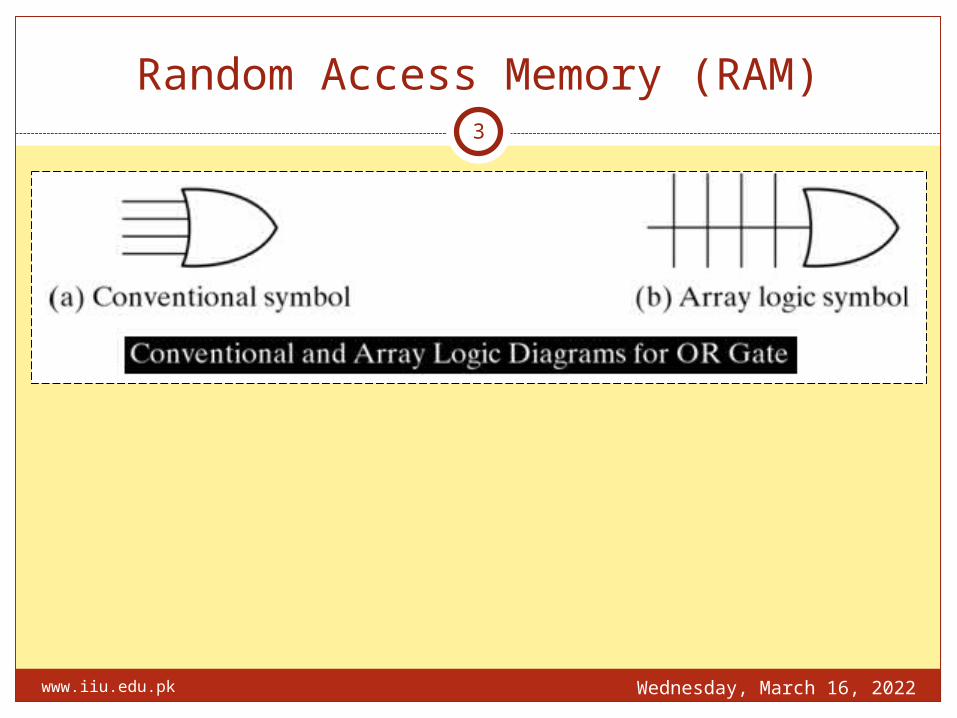
Random Access Memory (RAM)
Saturday, April 15, 2023
3
www.iiu.edu.pk

Saturday, April 15, 2023
Select R/W ’ Input Q Output Operation
0 0 0 Q(t) 0 No Operation
0 0 1 Q(t) 0 No Operation
0 1 0 Q(t) 0 No Operation
0 1 1 Q(t) 0 No Operation
1 0 0 0 0 Write 0
1 0 1 1 0 Write 1
1 1 0 Q(t) Q(t) Read Data
1 1 1 Q(t) Q(t) Read Data
Select R/W’ Operation
0 X No Operation
1 0 Memory Write
1 1 Memory Read
4
www.iiu.edu.pk
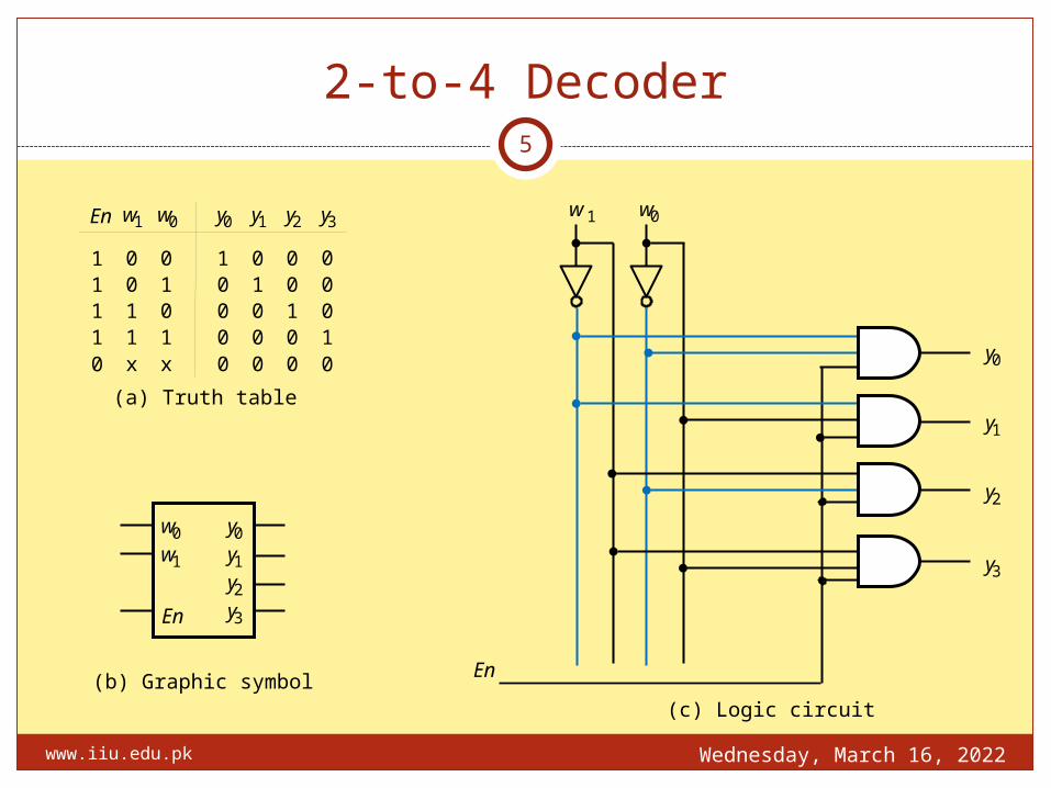
2-to-4 Decoder
Saturday, April 15, 2023
5
www.iiu.edu.pk
0 0 1 1
1 0 1
y 0 w 1
0
w 0
x x
1 1
0
1 1
En
0 0 0
1
0
y 1
1 0 0
0
0
y 2
0 1 0
0
0
y 3
0 0 1
0
0
(a) Truth table
w 0
En
y 0 w 1 y 1
y 2 y 3
(b) Graphic symbol (c) Logic circuit
w 1 w 0
En
y 0
y 1
y 2
y 3

Saturday, April 15, 2023
6
www.iiu.edu.pk

Question: How many address lines, input-output data lines are needed in each case of RAM size
(a) 8K×16 (b) 2G×8 (c) 16M×32 (d) 256K×64
Bus Size in RAM
Saturday, April 15, 2023
7
www.iiu.edu.pk
RAM Size: (a) 214 Bytes (b) 231 Bytes (c) 226 Bytes (d) 221 Bytes

Basic Types of RAM
Saturday, April 15, 2023www.iiu.edu.pk
8
Static RAM (SRAM)Stores data in latchesNo refreshingMore power
consumptionLess storage capacityUsed in
Microprocessor cache memory
volatile
Dynamic RAM (DRAM)Stores data in
capacitorsNeeds refreshingReduced power
consumptionLarge storage
capacityUsed in PC memory
on Mother Boardvolatile
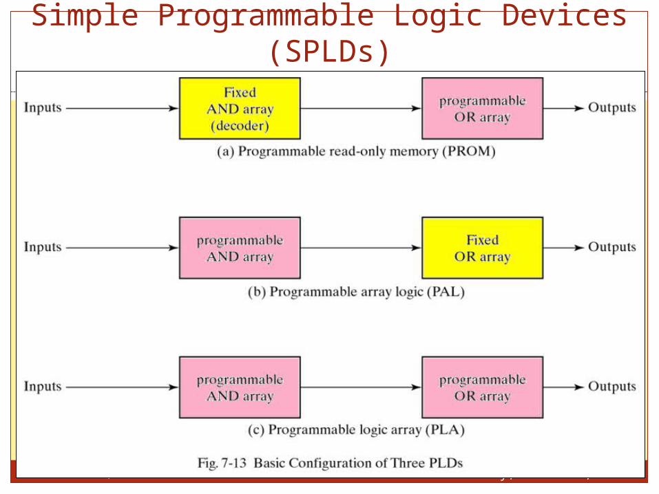
Simple Programmable Logic Devices (SPLDs)
Saturday, April 15, 2023
9
www.iiu.edu.pk

PROM (Programmable Read Only Memory)PROM has fixed AND array constructed as decoder and a
programmable OR array.The programmable OR gates implement the Boolean
functions in sum of min terms form.Initially PROM contains all the fuses intact, giving all 1’s.Fuses are blown by application of high voltage pulse.A blown fuse defines a binary 0 state and an intact fuse
gives a binary 1 state.
Simple Programmable Logic Devices (SPLDs)
Saturday, April 15, 2023
10
www.iiu.edu.pk
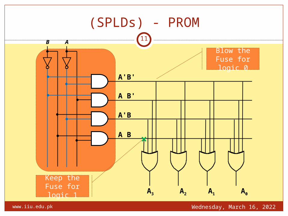
(SPLDs) - PROM
Saturday, April 15, 2023
11
www.iiu.edu.pk
B A
A'B'
A B'
A'B
A B
Blow the Fuse for logic 0
Keep the Fuse for logic 1
×
A3 A2 A1 A0

Question: Implements the following in PROM
A3 = A'B', A2 = A'B' + AB, A1 = (AB)', A0 = A+B
Answer: Convert all equations into sum of minterms
A3 = A'B'
A2 = A'B'+ AB
A1 = (AB)' = A'+B' = A'(B+B')+B'(A+A')
= A'B+ A'B'+ AB'+ A'B'
= A'B + AB' + A'B'
A0 = A+B = A(B+B')+B(A+A')= AB+AB'+AB+A'B
= AB + AB' + A'B
Logic Implementation in PROM
Saturday, April 15, 2023
12
www.iiu.edu.pk
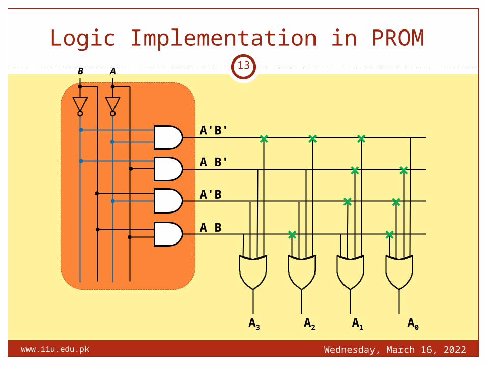
Logic Implementation in PROM
Saturday, April 15, 2023
13
www.iiu.edu.pk
B A
A'B'
A B'
A'B
A B
×
A3 A2 A1 A0
×
×
×
×
×
×
×
×
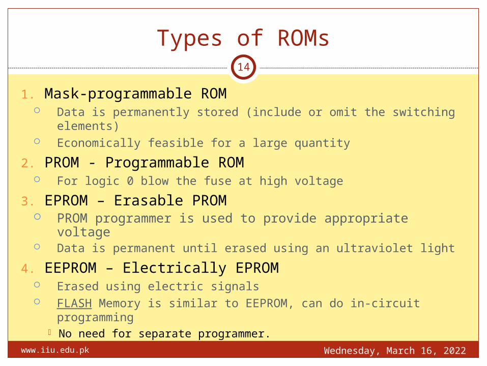
1. Mask-programmable ROM Data is permanently stored (include or omit the switching elements) Economically feasible for a large quantity
2. PROM - Programmable ROM For logic 0 blow the fuse at high voltage
3. EPROM – Erasable PROM PROM programmer is used to provide appropriate voltage Data is permanent until erased using an ultraviolet light
4. EEPROM – Electrically EPROM Erased using electric signals FLASH Memory is similar to EEPROM, can do in-circuit programming
No need for separate programmer.
Types of ROMs
Saturday, April 15, 2023
14
www.iiu.edu.pk
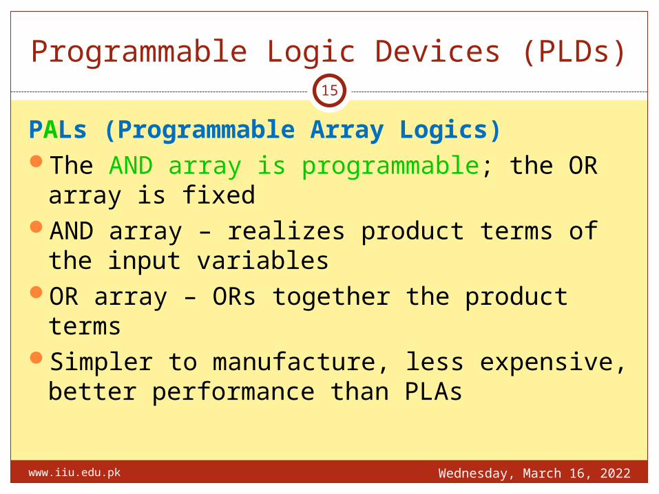
PALs (Programmable Array Logics)The AND array is programmable; the OR array is fixedAND array – realizes product terms of the input variablesOR array – ORs together the product termsSimpler to manufacture, less expensive, better
performance than PLAs
Programmable Logic Devices (PLDs)
Saturday, April 15, 2023
15
www.iiu.edu.pk
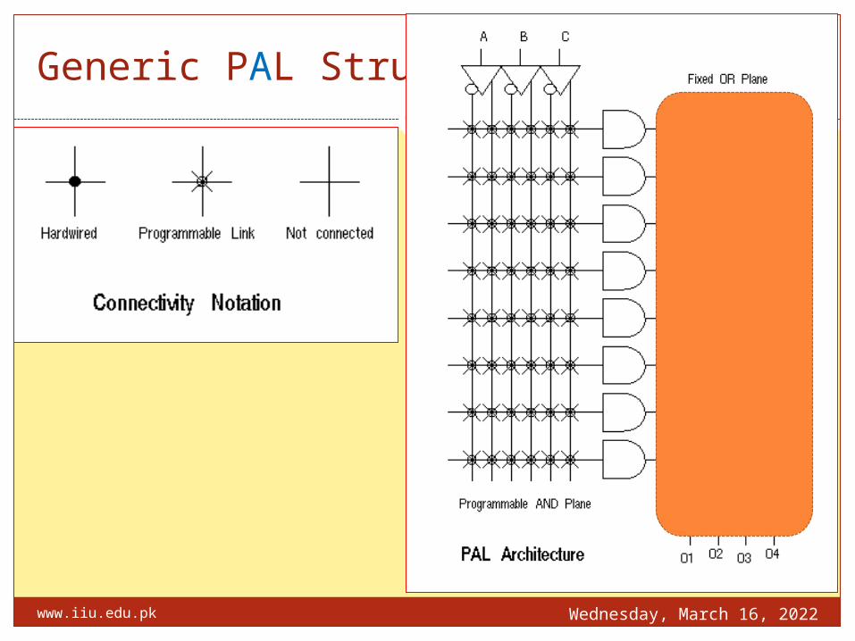
Generic PAL Structure
Saturday, April 15, 2023
16
www.iiu.edu.pk

Saturday, April 15, 202317
Typical PALs
Typical PALs have from 10 to 20 inputs from 2 to 10 outputs from 2 to 8 AND gates driving each OR gate often include D flip-flops
Select
f 1
Enable
To AND plane
D Q
Clock
Flip-flop
MUX output is “fed back” to the AND plane.
www.iiu.edu.pk

Saturday, April 15, 202318
Logic Diagram for 16R4 PAL
www.iiu.edu.pk

Saturday, April 15, 202319
Logic Diagram for 16R4 PAL
www.iiu.edu.pk

PLAs (Programmable Logic Arrays)Logic functions in Sum Of Product (SOP) formBoth AND and OR planes are programmable
AND array – realizes product terms of the input variables
OR array – ORs together the product terms
Programmable Logic Devices (PLDs)
Saturday, April 15, 2023
20
www.iiu.edu.pk

Generic PLA Structure
Saturday, April 15, 2023
21
www.iiu.edu.pk
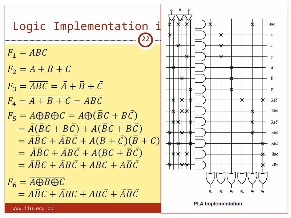
Logic Implementation in PLA
Saturday, April 15, 2023
22
www.iiu.edu.pk

Binary to Gray Code Conversion
Saturday, April 15, 2023www.iiu.edu.pk
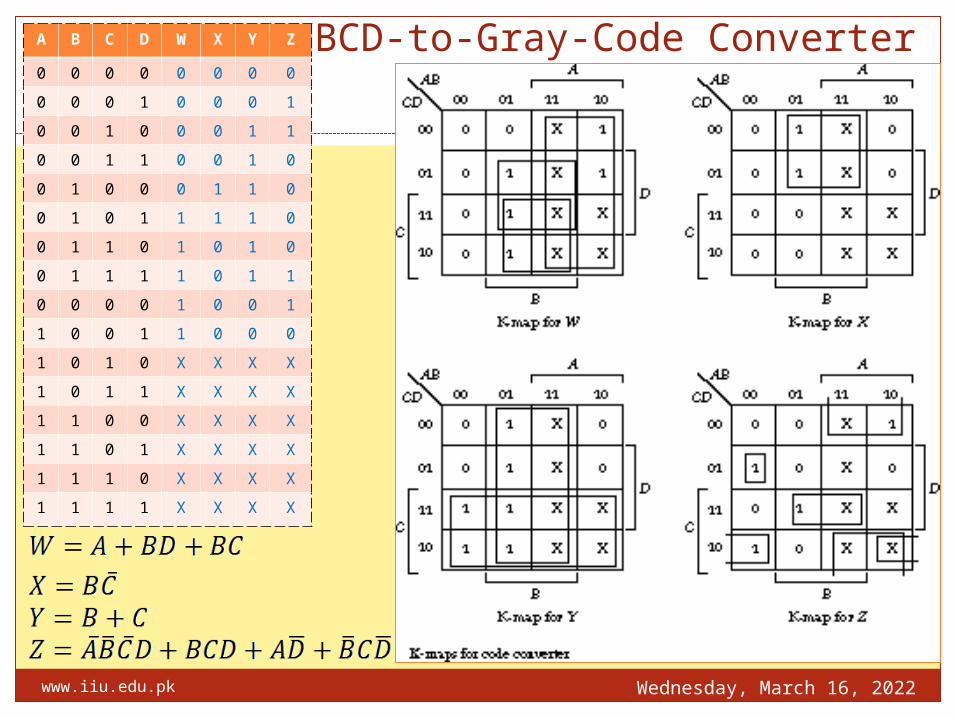
BCD-to-Gray-Code Converter
Saturday, April 15, 2023
24
www.iiu.edu.pk
A B C D W X Y Z
0 0 0 0 0 0 0 0
0 0 0 1 0 0 0 1
0 0 1 0 0 0 1 1
0 0 1 1 0 0 1 0
0 1 0 0 0 1 1 0
0 1 0 1 1 1 1 0
0 1 1 0 1 0 1 0
0 1 1 1 1 0 1 1
0 0 0 0 1 0 0 1
1 0 0 1 1 0 0 0
1 0 1 0 X X X X
1 0 1 1 X X X X
1 1 0 0 X X X X
1 1 0 1 X X X X
1 1 1 0 X X X X
1 1 1 1 X X X X
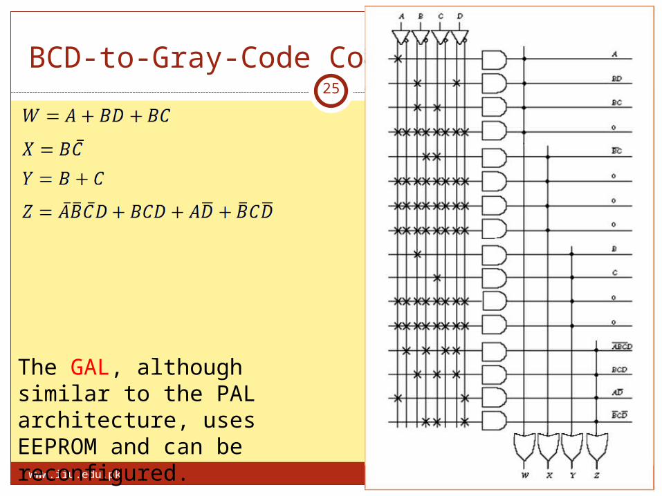
BCD-to-Gray-Code Converter in PLA
Saturday, April 15, 2023
25
www.iiu.edu.pk
The GAL, although similar to the PAL architecture, uses EEPROM and can be reconfigured.
PLAs are more flexible than PALs since both AND & OR planes are programmable in PLAs.
Because both AND & OR planes are programmable, PLAs are expensive to fabricate and have large propagation delay.
By using fix OR gates, PALs are cheaper and faster than PLAs. Logic expanders increase the flexibilities of PALs, but result in
significant propagation delay.PALs usually contain D flip-flops connected to the outputs of OR gates
to implement sequential circuits.PLAs and PALs are usually referred to as SPLD.
PLA v.s. PAL
Saturday, April 15, 2023
26
www.iiu.edu.pk