four 1-bit, 10mhz, 2nd-order delta-sigma modulators · pdf fileabsolute maximum ratings(1)...
TRANSCRIPT

1FEATURES DESCRIPTION
APPLICATIONS CH A+
AVDD
CH A- Output
Interface
Circuit
RC
Oscillator
20MHz
Out EN
Clock
Select
Divider
REFIN A
Reference
Voltage
2.5V
REFOUT
OUT A
OUT B
OUT C
OUT D
CLKIN
AGND BGND
BVDD
CLKOUT
CLKSEL
CH B+
CH B-
REFIN B
CH C+
CH C-
REFIN C
2nd-Order
DS Modulator
CH D+
CH D-
REFIN D
2nd-Order
DS Modulator
2nd-Order
DS Modulator
2nd-Order
DS Modulator
ADS1204
www.ti.com........................................................................................................................................... SBAS301C–OCTOBER 2003–REVISED FEBRUARY 2009
Four 1-Bit, 10MHz, 2nd-OrderDelta-Sigma Modulators
2• 16-Bit Resolution The ADS1204 is a four-channel, high-performancedevice, with four delta-sigma (ΔΣ) modulators with• 14-Bit Linearity100dB dynamic range, operating from a single +5V• Resolution/Speed Trade-Off: 10-Bit Effectivesupply. The differential inputs are ideal for directResolution with 10µs Signal Delay (12-Bit with connection to transducers in an industrial19µs) environment. With the appropriate digital filter and
• ±2.5V Input Range at 2.5V modulator rate, the device can be used to achieve16-bit analog-to-digital (A/D) conversion with no• Internal Reference Voltage: 2%missing code. Effective resolution of 12 bits can be• Gain Error: 0.5% obtained with a digital filter data rate of 160kHz at a
• Four Independent Delta-Sigma Modulators modulator rate of 10MHz. The ADS1204 is designedfor use in medium- to high-resolution measurement• Four Input Reference Buffersapplications including current measurements, smart• Onboard 20MHz Oscillator transmitters, industrial process control, weight scales,
• Selectable Internal or External Clock chromatography, and portable instrumentation. It isavailable in a QFN-32 (5×5) package.• Operating Temperature Range:
–40°C to +105°C• QFN-32 (5×5) Package
• Motor Control• Current Measurement• Industrial Process Control• Instrumentation• Smart Transmitters• Portable Instruments• Weight Scales• Pressure Transducers
1
Please be aware that an important notice concerning availability, standard warranty, and use in critical applications of TexasInstruments semiconductor products and disclaimers thereto appears at the end of this data sheet.
2All trademarks are the property of their respective owners.
PRODUCTION DATA information is current as of publication date. Copyright © 2003–2009, Texas Instruments IncorporatedProducts conform to specifications per the terms of the TexasInstruments standard warranty. Production processing does notnecessarily include testing of all parameters.

ABSOLUTE MAXIMUM RATINGS (1)
RECOMMENDED OPERATING CONDITIONS
ADS1204
SBAS301C–OCTOBER 2003–REVISED FEBRUARY 2009........................................................................................................................................... www.ti.com
This integrated circuit can be damaged by ESD. Texas Instruments recommends that all integrated circuits be handled withappropriate precautions. Failure to observe proper handling and installation procedures can cause damage.
ESD damage can range from subtle performance degradation to complete device failure. Precision integrated circuits may be moresusceptible to damage because very small parametric changes could cause the device not to meet its published specifications.
ORDERING INFORMATION (1)
MAXIMUMINTEGRALLINEARITY MAXIMUM SPECIFIED
ERROR GAIN PACKAGE- PACKAGE TEMPERATURE PACKAGE ORDERING TRANSPORTPRODUCT (LSB) ERROR (%) LEAD DESIGNATOR RANGE MARKING NUMBER MEDIA, QUANTITY
ADS1204IRHBT Tape and Reel, 250ADS1204 ±3 ±0.5 QFN-32 RHB –40°C to +105°C ADS1204I
ADS1204IRHBR Tape and Reel, 3000
(1) For the most current package and ordering information see the Package Option Addendum at the end of this document, or see the TIweb site at www.ti.com.
Over operating free-air temperature range, unless otherwise noted.
ADS1204 UNITSupply voltage, AVDD to AGND –0.3 to 6 VSupply voltage, BVDD to BGND –0.3 to 6 VAnalog input voltage with respect to AGND AGND – 0.3 to AVDD + 0.3 VReference input voltage with respect to AGND AGND – 0.3 to AVDD + 0.3 VDigital input voltage with respect to BGND BGND – 0.3 to BVDD + 0.3 VGround voltage difference, AGND to BGND ±0.3 VVoltage differences, BVDD to AGND –0.3 to 6 VInput current to any pin except supply ±10 mAPower dissipation See Dissipation Ratings tableOperating virtual junction temperature range, TJ –40 to +150 °CStorage temperature range, TSTG –65 to +150 °CLead temperature (1.6mm or 1/16″ from case for 10s) 260 °C
(1) Stresses beyond those listed under Absolute Maximum Ratings may cause permanent damage to the device. These are stress ratingsonly, and functional operation of the device at these or any other conditions beyond those indicated under Recommended OperatingConditions is not implied. Exposure to absolute-maximum-rated conditions for extended periods may affect device reliability.
PARAMETER MIN NOM MAX UNITSupply voltage, AVDD to AGND 4.75 5 5.25 V
Low-voltage levels 2.7 3.6 VSupply voltage, BVDD to BGND
5V logic levels 4.5 5 5.5 VReference input voltage 0.5 2.5 2.6 VOperating common-mode signal 0 AVDD VAnalog inputs +IN – (–IN) 0 ±REFIN VExternal clock (1) 16 20 24 MHzOperating free-air temperature range, TA –40 +125 °CSpecified free-air temperature range, TA –40 +105 °C
(1) With reduced accuracy, clock can go from 1MHz up to 32MHz; see Typical Characteristic curves.
2 Submit Documentation Feedback Copyright © 2003–2009, Texas Instruments Incorporated
Product Folder Link(s): ADS1204

DISSIPATION RATINGS
ELECTRICAL CHARACTERISTICS
ADS1204
www.ti.com........................................................................................................................................... SBAS301C–OCTOBER 2003–REVISED FEBRUARY 2009
DERATING FACTORTA ≤ +25°C ABOVE TA = TA = +70°C TA = +85°C TA = +105°C
PACKAGE POWER RATING +25°C (1) POWER RATING POWER RATING POWER RATINGQFN-32 (5×5) 3406mW 27.25mW/°C 2180mW 1771mW 1226mW
(1) This is the inverse of the traditional junction-to-ambient thermal resistance (RθJA). Thermal resistances are not production tested and arefor informational purposes only.
Over recommended operating free-air temperature range at –40°C to +105°C, AVDD = 5V, BVDD = 3V, CH x+ = 0.5V to 4.5V,CH x– = 2.5V, REFIN = REFOUT = internal +2.5V, CLKIN = 20MHz, and 16-bit Sinc3 filter with decimation by 256, unlessotherwise noted.
ADS1204PARAMETER TEST CONDITIONS MIN TYP (1) MAX UNIT
RESOLUTION 16 BitsDC ACCURACY
±1 ±3 LSBINL Integral linearity error (2)
±0.001 ±0.005 % FSR±6 LSB
Integral linearity match±0.009 % FSR
DNL Differential nonlinearity (3) ±1 LSBVOS Input offset error –1.4 ±3 mV
Input offset error match ±2 mVTCVOS Input offset error drift ±2 ±8 µV/°CGERR Gain error (4) Referenced to VREF ±0.08 ±0.5 % FSR
Gain error match ±0.185 ±0.5 % FSRTCGERR Gain error drift ±2 ppm/°CPSRR Power-supply rejection ratio 4.75V < AVDD < 5.25V 78 dBANALOG INPUTFSR Full-scale differential range (CH x+) – (CH x–); CH x– = 2.5V ±2.5 V
Specified differential range (CH x+) – (CH x–); CH x– = 2.5V ±2 VMaximum operating input range (3) 0 AVDD VInput capacitance Common-mode 1.5 pFInput leakage current CLK turned off ±1 nADifferential input resistance 100 kΩDifferential input capacitance 2.5 pF
At DC 100 dBCMRR Common-mode rejection ratio
VIN = ±1.25VPP at 40kHz 110 dBBW Bandwidth FS sine wave, –3dB 50 MHzSAMPLING DYNAMICS
Internal clock frequency CLKSEL = 1 8 10 12 MHzCLKIN External clock frequency CLKSEL = 0 1 20 24 MHz
(1) All typical values are at TA = +25°C.(2) Integral nonlinearity is defined as the maximum deviation of the line through the end points of the specified input range of the transfer
curve for CH x+ = –2V to +2V at 2.5V, expressed either as the number of LSBs or as a percent of measured input range (4V).(3) Specified by design.(4) Maximum values, including temperature drift, are specified over the full specified temperature range.
Copyright © 2003–2009, Texas Instruments Incorporated Submit Documentation Feedback 3
Product Folder Link(s): ADS1204

ADS1204
SBAS301C–OCTOBER 2003–REVISED FEBRUARY 2009........................................................................................................................................... www.ti.com
ELECTRICAL CHARACTERISTICS (continued)Over recommended operating free-air temperature range at –40°C to +105°C, AVDD = 5V, BVDD = 3V, CH x+ = 0.5V to 4.5V,CH x– = 2.5V, REFIN = REFOUT = internal +2.5V, CLKIN = 20MHz, and 16-bit Sinc3 filter with decimation by 256, unlessotherwise noted.
ADS1204PARAMETER TEST CONDITIONS MIN TYP (1) MAX UNIT
AC ACCURACYVIN = ±2VPP at 5kHz; –96 –88 dB–40°C ≤ TA ≤ +85°C
THD Total harmonic distortionVIN = ±2VPP at 5kHz; –96 –87 dB–40°C ≤ TA ≤ +105°C
SFDR Spurious-free dynamic range VIN = ±2VPP at 5kHz 92 100 dBSNR Signal-to-noise ratio VIN = ±2VPP at 5kHz 86 89 dBSINAD Signal-to-noise + distortion VIN = ±2VPP at 5kHz 85 89 dB
Channel-to-channel isolation (5) VIN = ±2VPP at 50kHz 85 dBENOB Effective number of bits 14 14.5 BitsVOLTAGE REFERENCE OUTPUTVOUT Reference voltage output 2.450 2.5 2.550 VdVOUT/dT Output voltage temperature drift ±20 ppm/°C
f = 0.1Hz to 10Hz, CL = 10µF 10 µVrmsOutput voltage noise
f = 10Hz to 10kHz, CL = 10µF 12 µVrmsPSRR Power-supply rejection ratio 60 dBIOUT Output current 10 µAISC Short-circuit current 0.5 mA
Turn-on settling time to 0.1% at CL = 0 100 µsVOLTAGE REFERENCE INPUTVIN Reference voltage input 0.5 2.5 2.6 V
Reference input resistance 100 MΩReference input capacitance 5 pFReference input current 1 µA
DIGITAL INPUTS (6)
Logic family CMOS with Schmitt TriggerVIH High-level input voltage 0.7 × BVDD BVDD + 0.3 VVIL Low-level input voltage –0.3 0.3 × BVDD VIIN Input current VI = BVDD or GND ±50 nACI Input capacitance 5 pFDIGITAL OUTPUTS (6)
Logic family CMOSVOH High-level output voltage BVDD = 4.5V, IOH = –100µA 4.44 VVOL Low-level output voltage BVDD = 4.5V, IOL = +100µA 0.5 VCO Output capacitance 5 pFCL Load capacitance 30 pF
Data format Bit stream
(5) Specified by design.(6) Applicable for 5.0V nominal supply: BVDD (min) = 4.5V and BVDD (max) = 5.5V.
4 Submit Documentation Feedback Copyright © 2003–2009, Texas Instruments Incorporated
Product Folder Link(s): ADS1204

R
650W
ONC
1pF(SAMPLE)
BVDD
DIN
BGND
AVDD
AIN
AGND
Diode Turn-On Voltage: 0.35V
Equivalent Digital Input CircuitEquivalent Analog Input Circuit
ADS1204
www.ti.com........................................................................................................................................... SBAS301C–OCTOBER 2003–REVISED FEBRUARY 2009
ELECTRICAL CHARACTERISTICS (continued)Over recommended operating free-air temperature range at –40°C to +105°C, AVDD = 5V, BVDD = 3V, CH x+ = 0.5V to 4.5V,CH x– = 2.5V, REFIN = REFOUT = internal +2.5V, CLKIN = 20MHz, and 16-bit Sinc3 filter with decimation by 256, unlessotherwise noted.
ADS1204PARAMETER TEST CONDITIONS MIN TYP (1) MAX UNIT
DIGITAL INPUTS (7)
Logic family LVCMOSVIH High-level input voltage BVDD = 3.6V 2 BVDD + 0.3 VVIL Low-level input voltage BVDD = 2.7V –0.3 0.8 VIIN Input current VI = BVDD or GND ±50 nACI Input capacitance 5 pFDIGITAL OUTPUTS (7)
Logic family LVCMOSVOH High-level output voltage BVDD = 2.7V, IOH = –100µA BVDD – 0.2 VVOL Low-level output voltage BVDD = 2.7V, IOL = +100µA 0.2 VCO Output capacitance 5 pFCL Load capacitance 30 pF
Data format Bit streamPOWER SUPPLYAVDD Analog supply voltage 4.5 5.5 V
Low-voltage levels 2.7 3.6 VBVDD Buffer I/O supply voltage
5V logic levels 4.5 5.5 VCLKSEL = 1 22.5 30 mA
AIDD Analog operating supply currentCLKSEL = 0 22.4 29 mABVDD = 3V, CLKOUT = 10MHz 4 mA
BIDD Buffer I/O operating supply currentBVDD = 5V, CLKOUT = 10MHz 4 mACLKSEL = 0 122 145 mW
Power dissipationCLKSEL = 1 112.5 150 mW
(7) Applicable for 3.0V nominal supply: BVDD (min) = 2.7V and BVDD (max) = 3.6V.
EQUIVALENT INPUT CIRCUITS
NOTE: The thermal pad is internally connected to the substrate. This pad can be connected to the analog ground or left floating. Keep thethermal pad separate from the digital ground, if possible.
Copyright © 2003–2009, Texas Instruments Incorporated Submit Documentation Feedback 5
Product Folder Link(s): ADS1204

PIN ASSIGNMENTS
CH A+
CH A-
CH B+
CH B-
CH C-
CH C+
CH D-
CH D+
OUT A
OUT B
OUT C
OUT D
CLKOUT
BGND
BVDD
CLKIN
1
2
3
4
5
6
7
8
24
23
22
21
20
19
18
17
ADS1204R
EF
IN A
32
RE
FIN
D9
RE
FIN
BR
EF
IN C
AG
ND
AG
ND
AV
DD
AV
DD
RE
FO
UT
NC
AV
DD
AV
DD
AG
ND
AG
ND
NC
CLK
SE
L
31
25
26
28
27
29
30
16
15
14
13
1211
10
ADS1204
SBAS301C–OCTOBER 2003–REVISED FEBRUARY 2009........................................................................................................................................... www.ti.com
RHB PACKAGE(1)
QFN-32(TOP VIEW)
(1) The thermal pad is internally connected to the substrate. This pad can be connected to the analog ground or left floating. Keep thethermal pad separate from the digital ground, if possible.
TERMINAL FUNCTIONSTERMINAL
NAME NO. I/O (1) DESCRIPTIONCH A+ 1 AI Analog input of channel A: noninverting inputCH A– 2 AI Analog input of channel A: inverting inputCH B+ 3 AI Analog input of channel B: noninverting inputCH B– 4 AI Analog input of channel B: inverting inputCH C– 5 AI Analog input of channel C: inverting inputCH C+ 6 AI Analog input of channel C: noninverting inputCH D– 7 AI Analog input of channel D: inverting inputCH D+ 8 AI Analog input of channel D: noninverting inputREFIN D 9 AI Reference voltage input of channel D: pin for external reference voltageREFIN C 10 AI Reference voltage input of channel C: pin for external reference voltageAGND 11 — Analog groundAVDD 12 P Analog power supply; nominal 5VNC 13 — No connection; this pin is left unconnectedAVDD 14 P Analog power supply; nominal 5VAGND 15 — Analog groundCLKSEL 16 I Clock select between internal clock (CLKSEL = 1) or external clock (CLKSEL = 0)CLKIN 17 I External clock inputBVDD 18 P Digital interface power supply; from 2.7V to 5.5VBGND 19 — Interface groundCLKOUT 20 O System clock output
(1) AI = Analog Input; AO = Analog Output; I = Input; O = Output; P = Power Supply.
6 Submit Documentation Feedback Copyright © 2003–2009, Texas Instruments Incorporated
Product Folder Link(s): ADS1204

ADS1204
www.ti.com........................................................................................................................................... SBAS301C–OCTOBER 2003–REVISED FEBRUARY 2009
TERMINAL FUNCTIONS (continued)TERMINAL
NAME NO. I/O (1) DESCRIPTIONOUT D 21 O Bit stream from channel D modulatorOUT C 22 O Bit stream from channel C modulatorOUT B 23 O Bit stream from channel B modulatorOUT A 24 O Bit stream from channel A modulatorNC 25 — No connection; this pin is left unconnectedAGND 26 — Analog groundAVDD 27 P Analog power supply; nominal 5VREFOUT 28 AO Reference voltage output: output pin of the internal reference source; nominal 2.5VAVDD 29 P Analog power supply; nominal 5VAGND 30 — Analog groundREFIN B 31 AI Reference voltage input of channel B: pin for external reference voltageREFIN A 32 AI Reference voltage input of channel A: pin for external reference voltage
Copyright © 2003–2009, Texas Instruments Incorporated Submit Documentation Feedback 7
Product Folder Link(s): ADS1204

PARAMETER MEASUREMENT INFORMATION
CLKOUT
OUT x
tC1
tW2tD4tD3
tC2tW1tD1 tD2
CLKIN
TIMING REQUIREMENTS: 5.0V (1)
TIMING REQUIREMENTS: 3.0V (1)
ADS1204
SBAS301C–OCTOBER 2003–REVISED FEBRUARY 2009........................................................................................................................................... www.ti.com
Figure 1. ADS1204 Timing Diagram
Over recommended operating free-air temperature range at –40°C to +105°C, AVDD = 5V, and BVDD = 5V, unless otherwisenoted.
PARAMETER MIN MAX UNITtC1 CLKIN period 41.6 1000 nstW1 CLKIN high time 10 tC1 – 10 nstC2 CLKOUT period using internal oscillator (CLKSEL = 1) 83 125 ns
CLKOUT period using external clock (CLKSEL = 0) 2 × tC1 nstW2 CLKOUT high time (tC2/2) – 5 (tC2/2) + 5 nstD1 CLKOUT rising edge delay after CLKIN rising edge 0 10 nstD2 CLKOUT falling edge delay after CLKIN rising edge 0 10 nstD3 Data valid delay after rising edge of CLKOUT (CLKSEL = 1) (tC2/4) – 8 (tC2/4) + 8 nstD4 Data valid delay after rising edge of CLKOUT (CLKSEL = 0) tW1 – 3 tW1 + 7 ns
(1) Applicable for 5.0V nominal supply: BVDD (min) = 4.5V and BVDD (max) = 5.5V. All input signals are specified with tR = tF = 5ns (10% to90% of BVDD) and timed from a voltage level of (VIL + VIH)/2. See Figure 1.
Over recommended operating free-air temperature range at –40°C to +105°C, AVDD = 5V, and BVDD = 5V, unless otherwisenoted.
PARAMETER MIN MAX UNITtC1 CLKIN period 41.6 1000 nstW1 CLKIN high time 10 tC1 – 10 nstC2 CLKOUT period using internal oscillator (CLKSEL = 1) 83 125 ns
CLKOUT period using external clock (CLKSEL = 0) 2 × tC1 nstW2 CLKOUT high time (tC2/2) – 5 (tC2/2) + 5 nstD1 CLKOUT rising edge delay after CLKIN rising edge 0 10 nstD2 CLKOUT falling edge delay after CLKIN rising edge 0 10 nstD3 Data valid delay after rising edge of CLKOUT (CLKSEL = 1) (tC2/4) – 8 (tC2/4) + 8 nstD4 Data valid delay after rising edge of CLKOUT (CLKSEL = 0) tW1 – 3 tW1 + 7 ns
(1) Applicable for 3.0V nominal supply: BVDD (min) = 2.7V and BVDD (max) = 3.6V. All input signals are specified with tR = tF = 5ns (10% to90% of BVDD) and timed from a voltage level of (VIL + VIH)/2. See Figure 1.
8 Submit Documentation Feedback Copyright © 2003–2009, Texas Instruments Incorporated
Product Folder Link(s): ADS1204

TYPICAL CHARACTERISTICS
0-2.0 -1.0 -0.5-1.5 0.5 1.51.0 2.0
Differential Input Voltage (V)
INL
(LS
B)
1.5
1.0
0.5
0
0.5
1.0
1.5
-
-
-
+25 C°
- °40 C
+85 C°
+105 C°
+125 C°
0-2.0 -1.0 -0.5-1.5 0.5 1.51.0 2.0
Differential Input Voltage (V)
INL
(LS
B)
1.5
1.0
0.5
0
0.5
1.0
1.5
-
-
-
+25 C°
- °40 C
+85 C°
+105 C°
+125 C°
0-2.0 -1.0 -0.5-1.5 0.5 1.51.0 2.0
Differential Input Voltage (V)
INL
(LS
B)
INL
(%)
0.4
0.3
0.2
0.1
0
0.1
0.2
0.3
0.4
-
-
-
-
0.00061
0.00046
0.00031
0.00015
0
0.00015
0.00031
0.00046
0.00061
-
-
-
-
CLKIN = 32MHz
CLKIN = 20MHz
20-40 -10 5-25 35 6550 125
Temperature ( C)°
INL
(LS
B)
1.5
1.2
0.9
0.6
0.3
01109580
External 32MHz Clock
External 20MHz Clock
20-40 -10 5-25 35 6550 125
Temperature ( C)°
Offset V
oltage (
mV
)
-1.20
1.25
1.30
1.35
1.40
1.45
1.50
1.55
1.60
-
-
-
-
-
-
-
-
1109580
External 32MHz Clock
External 20MHz Clock
20-40 -10 5-25 35 6550 125
Temperature ( C)°
Off
se
t M
atc
h (
mV
)
0.45
0.44
0.43
0.42
0.41
0.40
0.39
0.38
0.37
0.36
0.351109580
External 32MHz Clock
External 20MHz Clock
ADS1204
www.ti.com........................................................................................................................................... SBAS301C–OCTOBER 2003–REVISED FEBRUARY 2009
AVDD = 5V, BVDD = 3V, CH x+ = +0.5V to +4.5V, CH x– = +2.5V, REFIN = external, CLKSEL = 0, and 16-bit Sinc3 filter, withOSR = 256, unless otherwise noted.
INTEGRAL NONLINEARITY vs INPUT SIGNAL INTEGRAL NONLINEARITY vs INPUT SIGNAL(CLKIN = 20MHz) (CLKIN = 32MHz)
Figure 2. Figure 3.
INTEGRAL LINEARITY MATCH OF CHANNELS MAXIMUM INTEGRAL NONLINEARITYvs INPUT SIGNAL vs TEMPERATURE
Figure 4. Figure 5.
OFFSET vs TEMPERATURE OFFSET MATCH vs TEMPERATURE
Figure 6. Figure 7.
Copyright © 2003–2009, Texas Instruments Incorporated Submit Documentation Feedback 9
Product Folder Link(s): ADS1204

20-40 -10 5-25 35 6550 125
Temperature ( C)°
Re
fere
nce
Vo
lta
ge
(V
)
2.530
2.528
2.526
2.524
2.522
2.520
2.518
2.516
2.514
2.512
2.51011095804.5 4.6 4.7 4.8 4.9 5.0 5.1 5.2 5.3 5.4 5.5
Power Supply (V)
Offset (m
V)
-1.2
-
-
-
-
-
1.3
1.4
1.5
1.6
1.7
CLKIN = 20MHz
CLKIN = 32MHz
20-40 -10 5-25 35 6550 125
Temperature ( C)°
Gain
Err
or
(%)
1.0
0.9
0.8
0.7
0.6
0.5
0.4
0.3
0.2
0.1
01109580
External 32MHz Clock
External 20MHz Clock
20-40 -10 5-25 35 6550 125
Temperature ( C)°
Ga
in M
atc
h (
%)
0.24
0.23
0.22
0.21
0.20
0.19
0.18
0.17
0.16
0.151109580
External 32MHz Clock
External 20MHz Clock
20-40 -10 5-25 35 6550 125
Temperature ( C)°
Sig
na
l-to
-No
ise
Ra
tio
(d
B)
89.5
89.4
89.3
89.2
89.1
89.0
88.9
88.8
88.7
88.6
88.51109580
CLKIN = 20MHz
CLKIN = 32MHz
4V
5kHzPP
20-40 -10 5-25 35 6550 125
Temperature ( C)°
Sig
na
l-to
-No
ise
+ D
isto
rtio
n (
dB
)
89.2
89.0
88.8
88.6
88.4
88.2
88.0
87.8
87.6
1109580
CLKIN = 20MHz
CLKIN = 32MHz
4V
5kHzPP
ADS1204
SBAS301C–OCTOBER 2003–REVISED FEBRUARY 2009........................................................................................................................................... www.ti.com
TYPICAL CHARACTERISTICS (continued)AVDD = 5V, BVDD = 3V, CH x+ = +0.5V to +4.5V, CH x– = +2.5V, REFIN = external, CLKSEL = 0, and 16-bit Sinc3 filter, withOSR = 256, unless otherwise noted.
OFFSET vs POWER SUPPLY INTERNAL REFERENCE vs TEMPERATURE
Figure 8. Figure 9.
GAIN ERROR vs TEMPERATURE GAIN MATCH vs TEMPERATURE
Figure 10. Figure 11.
SNR vs TEMPERATURE SINAD vs TEMPERATURE
Figure 12. Figure 13.
10 Submit Documentation Feedback Copyright © 2003–2009, Texas Instruments Incorporated
Product Folder Link(s): ADS1204

20-40 -10 5-25 35 6550 125
Temperature ( C)°
Tota
l H
arm
on
ic D
isto
rtio
n (
dB
)
-85
87
89
91
93
95
97
99
101
103
105
-
-
-
-
-
-
-
-
-
-
1109580
CLKIN = 32MHz
CLKIN = 20MHz
4V
5kHzPP
20-40 -10 5-25 35 6550 125
Temperature ( C)°
Spurious-F
ree D
ynam
ic R
ange (
dB
)
105
103
101
99
97
95
93
91
89
87
851109580
CLKIN = 32MHz
CLKIN = 20MHz
4V
5kHzPP
1 10 100
Frequency (kHz)
SF
DR
(dB
) TH
D (d
B)
120
110
100
90
80
70
60
-120
-
-
-
-
-
-
110
100
90
80
70
60
THD
SFDR
1 10 100
Frequency (kHz)
SF
DR
(dB
) TH
D (d
B)
120
110
100
90
80
70
60
-120
-
-
-
-
-
-
110
100
90
80
70
60
THD
SFDR
0
-20
-40
-60
-80
-100
-120
-140
-160
-180
Magnitude (
dB
)
Frequency (kHz)
0 2 4 6 8 10 12 14 16 18 19
0
-20
-40
-60
-80
-100
-120
-140
-160
-180
Magnitude (
dB
)
Frequency (kHz)
0 2 4 6 8 10 12 14 16 18 19
ADS1204
www.ti.com........................................................................................................................................... SBAS301C–OCTOBER 2003–REVISED FEBRUARY 2009
TYPICAL CHARACTERISTICS (continued)AVDD = 5V, BVDD = 3V, CH x+ = +0.5V to +4.5V, CH x– = +2.5V, REFIN = external, CLKSEL = 0, and 16-bit Sinc3 filter, withOSR = 256, unless otherwise noted.
THD vs TEMPERATURE SFDR vs TEMPERATURE
Figure 14. Figure 15.
SFDR AND THD vs INPUT FREQUENCY SFDR AND THD vs INPUT FREQUENCY(CLKIN = 20MHz) (CLKIN = 32MHz)
Figure 16. Figure 17.
FREQUENCY SPECTRUM FREQUENCY SPECTRUM(4096 Point FFT, fIN = 1kHz, 4VPP) (4096 Point FFT, fIN = 5kHz, 4VPP)
Figure 18. Figure 19.
Copyright © 2003–2009, Texas Instruments Incorporated Submit Documentation Feedback 11
Product Folder Link(s): ADS1204
10 100 1k 10k
Decimation Ratio (OSR)
EN
OB
(B
its) S
NR
(dB
)
18
16
14
12
10
8
6
4
110
98
86
74
62
50
38
26
Sinc Filter3
Sinc Filter2
20-40 -10 5-25 35 6550 125
Temperature ( C)°
Cu
rre
nt
(mA
)
30
27
24
21
18
151109580
Internal Clock
External 20MHz Clock
External 32MHz Clock
1 10 100
Input Frequency (kHz)
CM
RR
(d
B)
110
105
100
95
90
85
80
75
70
65
60100 1k 10k 100k
Frequency of Power Supply (Hz)
PS
RR
(d
B)
110
100
90
80
70
60
50
20-40 -10 5-25 35 6550 125
Temperature ( C)°
Fre
quency (
MH
z)
10.0
9.8
9.6
9.4
9.2
9.0
8.8
8.6
8.4
8.2
8.01109580 4.5 4.7 4.9 5.1 5.3 5.5
Power Supply (V)
CL
KO
UT
(M
Hz)
9.8
9.7
9.6
9.5
9.4
9.3
9.2
ADS1204
SBAS301C–OCTOBER 2003–REVISED FEBRUARY 2009........................................................................................................................................... www.ti.com
TYPICAL CHARACTERISTICS (continued)AVDD = 5V, BVDD = 3V, CH x+ = +0.5V to +4.5V, CH x– = +2.5V, REFIN = external, CLKSEL = 0, and 16-bit Sinc3 filter, withOSR = 256, unless otherwise noted.
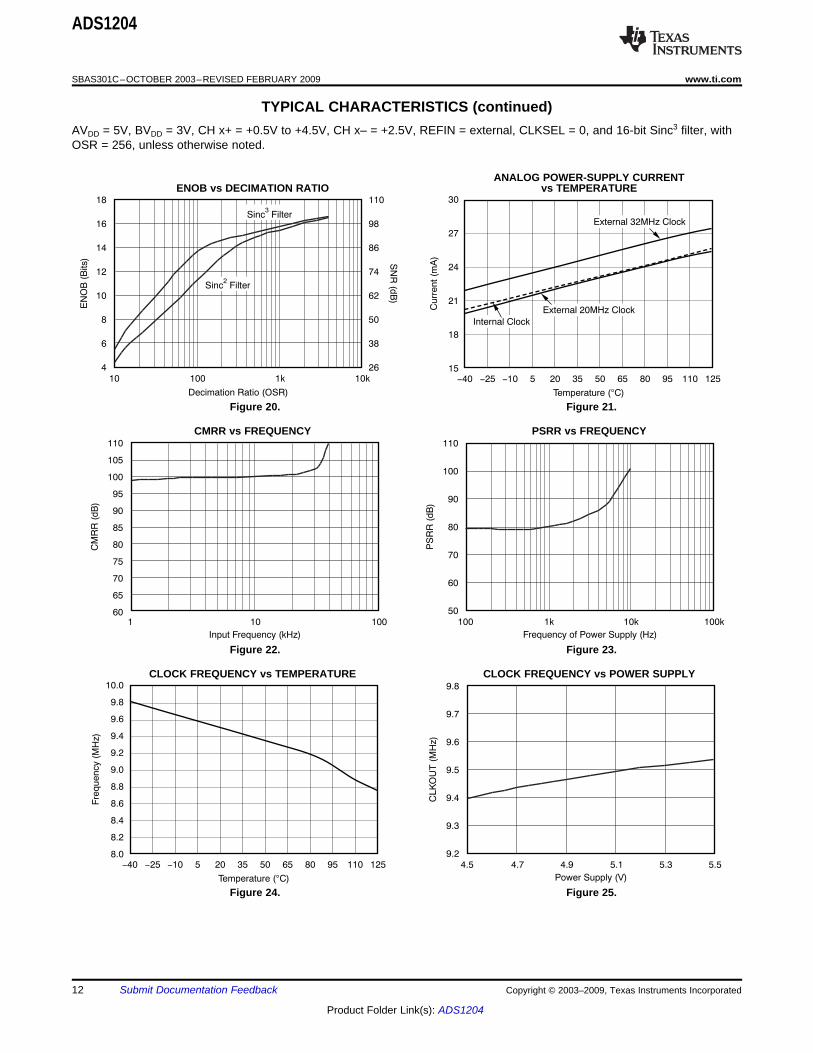
ANALOG POWER-SUPPLY CURRENTENOB vs DECIMATION RATIO vs TEMPERATURE
Figure 20. Figure 21.
CMRR vs FREQUENCY PSRR vs FREQUENCY
Figure 22. Figure 23.
CLOCK FREQUENCY vs TEMPERATURE CLOCK FREQUENCY vs POWER SUPPLY
Figure 24. Figure 25.
12 Submit Documentation Feedback Copyright © 2003–2009, Texas Instruments Incorporated
Product Folder Link(s): ADS1204

GENERAL DESCRIPTION
27W
5kW
5kW 2kW
2 kW
+5V
0.1nF
+3V
+3V
0.1 Fm
0.1 Fm
0.1 Fm
±5V
OPA43500.1 Fm
27W
5kW
5kW 2kW
2kW
+5V
0.1nF
±5V
OPA43500.1 Fm
FPGA
or
ASIC
CH A+
AVDD
CH A- Output
Interface
Circuit
RC
Oscillator
20MHz
Out EN
Clock
Select
Divider
REFIN A
Reference
Voltage
2.5V
REFOUT
OUT A
OUT B
OUT C
OUT D
CLKIN
AGNDAGNDAGNDAGND
BVDD
CLKOUT
BVDD
BGND
+5V
0.1 Fm+5V
0.1 Fm+5V
0.1 Fm+5V
0.1 Fm
CLKSEL
AVDD
AVDD
AVDD
AVDD
CH B+
CH B-
REFIN B
CH C+
CH C-
REFIN C
2nd-Order
DS Modulator
CH D+
CH D-
REFIN D
27W
5kW
5kW 2kW
2kW
+5V
0.1nF
±5V
OPA43500.1 Fm
27W
5kW
5kW 2kW
2kW
+5V
+5V0.1nF
±5V
OPA4350
OPA336
0.1 Fm
2nd-Order
DS Modulator
2nd-Order
DS Modulator
2nd-Order
DS Modulator
ADS1204
www.ti.com........................................................................................................................................... SBAS301C–OCTOBER 2003–REVISED FEBRUARY 2009
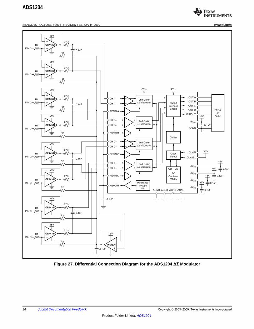
The ADS1204 is a four-channel, second-order, An application-specific integrated circuit (ASIC) orCMOS device with four delta-sigma (ΔΣ) modulators, field-programmable gate array (FPGA) could be useddesigned for medium- to high-resolution A/D signal to implement the digital filter. Figure 26 and Figure 27conversions from dc to 39kHz (filter response –3dB) if show typical application circuits with the ADS1204an oversampling ratio (OSR) of 64 is chosen. The connected to an FPGA.output of the converter (OUTX) provides a stream of The overall performance (that is, speed anddigital ones and zeros. The time average of this serial accuracy) depends on the selection of an appropriateoutput is proportional to the analog input voltage. OSR and filter type. A higher OSR produces greaterThe modulator shifts the quantization noise to high output accuracy while operating at a lower refreshfrequencies. A low-pass digital filter should be used rate. Alternatively, a lower OSR produces lowerat the output of the ΔΣ modulator. The filter serves output accuracy, but operates at a higher refreshtwo functions. First, it filters out high-frequency noise. rate. This system allows flexibility with the digital filterSecond, the filter converts the 1-bit data stream at a design and is capable of A/D conversion results thathigh sampling rate into a higher-bit data word at a have a dynamic range exceeding 100dB with an OSRlower rate (decimation). equal to 256.
Figure 26. Single-Ended Connection Diagram for the ADS1204 ΔΣ Modulator
Copyright © 2003–2009, Texas Instruments Incorporated Submit Documentation Feedback 13
Product Folder Link(s): ADS1204
+3V
+3V
0.1 Fm
0.1 Fm
0.1 Fm
27W
R1
R2
+5V
0.1nFIN+
IN-
OPA4354
27W
R1
R2
+5V
OPA4354
FPGA
or
ASIC
CH A+
AVDD
CH A- Output
Interface
Circuit
RC
Oscillator
20MHz
Out EN
Clock
Select
Divider
REFIN A
Reference
Voltage
2.5V
REFOUT
OUT A
OUT B
OUT C
OUT D
CLKIN
AGNDAGNDAGNDAGND
BVDD
CLKOUT
BVDD
BGND
+5V
0.1 Fm+5V
0.1 Fm+5V
0.1 Fm+5V
0.1 Fm
CLKSEL
AVDD
AVDD
AVDD
AVDD
CH B+
CH B-
REFIN B
CH C+
CH C-
REFIN C
2nd-Order
DS Modulator
CH D+
CH D-
REFIN D
27W
R1
R2
+5V
0.1nFIN+
IN-
OPA4354
27W
R1
R2
+5V
OPA4354
27W
R1
R2
+5V
0.1nFIN+
IN-
OPA4354
27W
R1
R2
+5V
OPA4354
27W
R1
R2
+5V
0.1nFIN+
IN-
OPA4354
27W
R1
R2
+5V
OPA4354
+5V
OPA336
2nd-Order
DS Modulator
2nd-Order
DS Modulator
2nd-Order
DS Modulator
ADS1204
SBAS301C–OCTOBER 2003–REVISED FEBRUARY 2009........................................................................................................................................... www.ti.com
Figure 27. Differential Connection Diagram for the ADS1204 ΔΣ Modulator
14 Submit Documentation Feedback Copyright © 2003–2009, Texas Instruments Incorporated
Product Folder Link(s): ADS1204

THEORY OF OPERATION
Z =IN
100kW
f /10MHzMOD (1)
ANALOG INPUT STAGE
Analog Input
650W
650W
Switching Frequency = CLK
High
Impedance
> 1GW1.2pF
VCM
AIN+
1.2pF
0.4pF
0.4pF
AIN-
High
Impedance
> 1GW
ADS1204
www.ti.com........................................................................................................................................... SBAS301C–OCTOBER 2003–REVISED FEBRUARY 2009
which is also the sampling frequency of themodulator. Figure 28 shows the basic input structureThe differential analog input of the ADS1204 is of one channel of the ADS1204. The relationshipimplemented with a switched-capacitor circuit. This between the input impedance of the ADS1204 andcircuit implements a second-order modulator stage, the modulator clock frequency is shown inwhich digitizes the analog input signal into a 1-bit Equation 1:output stream. The clock source can be internal as
well as external. Different frequencies for this clockallow for a variety of solutions and signal bandwidths.Every analog input signal is continuously sampled by
The input impedance becomes a consideration inthe modulator and compared to a reference voltagedesigns where the source impedance of the inputthat is applied to the REFINx pin. A digital stream,signal is high. This high impedance may causewhich accurately represents the analog input voltagedegradation in gain, linearity, and THD. Theover time, appears at the output of the correspondingimportance of this effect depends on the desiredconverter.system performance. There are two restrictions onthe analog input signals, CH x+ and CH x–. If theinput voltage exceeds the range (GND – 0.3V) to(VDD + 0.3V), the input current must be limited to10mA because the input protection diodes on the
The topology of the analog inputs of ADS1204 is front end of the converter will begin to turn on. Inbased on fully differential switched-capacitor addition, the linearity and the noise performance ofarchitecture. This input stage provides the the device are ensured only when the differentialmechanism to achieve low system noise, high analog voltage resides within ±2V (with VREF as acommon-mode rejection (100dB), and excellent midpoint); however, the FSR input voltage is ±2.5V.power-supply rejection.
The input impedance of the analog input isdependent on the modulator clock frequency (fCLK),
Figure 28. Input Impedance of the ADS1204
Copyright © 2003–2009, Texas Instruments Incorporated Submit Documentation Feedback 15
Product Folder Link(s): ADS1204

Modulator
DIGITAL OUTPUT
VREF
X4
X6
Integrator 2
Comparator
fCLK
DATA
D/A Converter
X3X2X(t)
fS
Integrator 1
Modulator Output
Analog Input
+FS (Analog Input)
-FS (Analog Input)
ADS1204
SBAS301C–OCTOBER 2003–REVISED FEBRUARY 2009........................................................................................................................................... www.ti.com
clock pulse by changing its analog output voltage atX6, causing the integrators to progress in theThe ADS1204 can be operated in two modes. When opposite direction. The feedback of the modulator toCKLSEL = 1, the four modulators operate using the the front end of the integrators forces the value of theinternal clock, which is fixed at 20MHz. When integrator output to track the average of the input.CKLSEL = 0, the modulators operate using an
external clock . In both modes, the clock is divided bytwo internally and functions as the modulator clock.The frequency of the external clock can vary from A differential input signal of 0V will ideally produce a1MHz to 32MHz to adjust for the clock requirements stream of ones and zeros that are high 50% of theof the application. time and low 50% of the time. A differential input of
+2V produces a stream of ones and zeros that areThe modulator topology is fundamentally ahigh 80% of the time. A differential input of –2Vsecond-order, switched-capacitor, ΔΣ modulator,produces a stream of ones and zeros that are highsuch as the one conceptualized in Figure 29. The20% of the time. The input voltage versus the outputanalog input voltage and the output of the 1-bitmodulator signal is shown in Figure 30.digital-to-analog converter (DAC) are differentiated,
providing analog voltages at X2 and X3. The voltagesat X2 and X3 are presented to their individualintegrators. The output of these integratorsprogresses in a negative or positive direction. Whenthe value of the signal at X4 equals the comparatorreference voltage, the output of the comparatorswitches from negative to positive, or positive tonegative, depending on its original state. When theoutput value of the comparator switches from high tolow or vice versa, the 1-bit DAC responds on the next
Figure 29. Block Diagram of the Second-Order Modulator
Figure 30. Analog Input vs Modulator Output of the ADS1204
16 Submit Documentation Feedback Copyright © 2003–2009, Texas Instruments Incorporated
Product Folder Link(s): ADS1204

DIGITAL INTERFACE
INTRODUCTION
MODES OF OPERATION 0
-10
-20
-30
-40
-50
-60
-70
-80
Gain
(dB
)
Frequency (kHz)
0 200 400 600 800 1000 1200 1400 1600
OSR = 32
f = 10MHz/32 = 312.5kHz
3dB: 81.9kHzDATA
-
FILTER USAGE
H(z) =1 z-
-OSR
1 z--1
2
(2)
30k
25k
20k
15k
10k
5k
0
Outp
ut C
ode
Number of Output Clocks
0 5 10 15 20 25 30 35 40
OSR = 32
FSR = 32768
ENOB = 9.9 Bits
Settling Time =
3 1/f = 9.6 s´ mDATA
ADS1204
www.ti.com........................................................................................................................................... SBAS301C–OCTOBER 2003–REVISED FEBRUARY 2009
frequency of output data rate fDATA = fCLK/OSR. The–3dB point is located at half the Nyquist frequency orfDATA/4. For some applications, it may be necessary
The analog signal connected to the input of the ΔΣ to use another filter type for better frequencymodulator is converted using the clock signal applied response.to the modulator. The result of the conversion, or
This performance can be improved, for example, by amodulation, is generated and sent to the OUTx pincascaded filter structure. The first decimation stagefrom the ΔΣ modulator. In most applications where acan be a Sinc3 filter with a low OSR and the seconddirect connection is realized between the ΔΣstage a high-order filter.modulator and an ASIC or FPGA (each with an
implemented filter), the two standard signals per For more information, see application note SBAA094,modulator (CLKOUT and OUTx) are provided from Combining the ADS1202 with an FPGA Digital Filterthe modulator. The output clock signal is equal for all for Current Measurement in Motor Controlfour modulators. If CLKSEL = 1, CLKIN must always Applications, available for download at www.ti.com.be set either high or low.
The system clock of the ADS1204 is 20MHz bydefault. The system clock can be provided either fromthe internal 20MHz RC oscillator or from an externalclock source. For this purpose, the CLKIN pin isprovided; it is controlled by the mode setting,CLKSEL.
The system clock is divided by two for the modulatorclock. Therefore, the default clock frequency of themodulator is 10MHz. With a possible external clockrange of 1MHz to 32MHz, the modulator operatesbetween 500kHz and 16MHz.
Figure 31. Frequency Response of Sinc3 FilterThe modulator generates only a bitstream, whichdoes not output a digital word like an A/D converter.In order to output a digital word equivalent to theanalog input voltage, the bitstream must beprocessed by a digital filter.
A very simple filter, built with minimal effort andhardware, is the Sinc3 filter shown in Equation 2:
This filter provides the best output performance at thelowest hardware size (for example, a count of digitalgates). For oversampling ratios in the range of 16 to256, this is a good choice. All the characterizations inthe data sheet are also done using a Sinc3 filter withan oversampling ratio of OSR = 256 and an output Figure 32. Pulse Response of Sinc3 Filterword width of 16 bits. (fMOD = 10MHz)In a Sinc3 filter response (shown in Figure 31 andFigure 32), the location of the first notch occurs at the
Copyright © 2003–2009, Texas Instruments Incorporated Submit Documentation Feedback 17
Product Folder Link(s): ADS1204

SNR = 1.76dB + 6.02dB ENOB´ (3) H(z) =1 z-
-OSR
1 z--1
(1 + z )- ´2 OSR
2
(4)
1 10 100 1000
OSR
EN
OB
(B
its)
16
14
12
10
8
6
4
2
0
Sincfast
Sinc3
Sinc
Sinc2
0 2 6 84 10
Settling Time (ms)E
NO
B (
Bits)
10
9
8
7
6
5
4
3
2
1
0
Sincfast
Sinc3
Sinc
Sinc2
ADS1204
SBAS301C–OCTOBER 2003–REVISED FEBRUARY 2009........................................................................................................................................... www.ti.com
The effective number of bits (ENOB) can be used to protection, filter types other than Sinc3 might be acompare the performance of A/D converters and ΔΣ better choice. A simple example is a Sinc2 filter.modulators. Figure 33 shows the ENOB of the Figure 34 compares the settling time of different filterADS1204 with different filter types. In this data sheet, types. The Sincfast is a modified Sinc2 filter asthe ENOB is calculated from the SNR as shown in Equation 4 shows:Equation 3:
Figure 33. Measured ENOB vs OSR
Figure 34. Measured ENOB vs Settling TimeIn motor control applications, a very fast responsetime for overcurrent detection is required. There is a
For more information, see application note SBAA094,constraint between 1µs and 5µs with 3 bits to 7 bitsCombining the ADS1202 with an FPGA Digital Filterresolution. The time for full settling is dependent onfor Current Measurement in Motor Controlthe filter order. Therefore, the full settling of the Sinc3
Applications, available for download at www.ti.com.filter needs three data clocks and the Sinc2 filterneeds two data clocks. The data clock is equal to themodulator clock divided by the OSR. For overcurrent
18 Submit Documentation Feedback Copyright © 2003–2009, Texas Instruments Incorporated
Product Folder Link(s): ADS1204

LAYOUT CONSIDERATIONS
POWER SUPPLIES DECOUPLING
GROUNDING
ADS1204
www.ti.com........................................................................................................................................... SBAS301C–OCTOBER 2003–REVISED FEBRUARY 2009
An applied external digital filter rejects high-frequency Good decoupling practices must be used for thenoise. PSRR and CMRR improve at higher ADS1204 and for all components in the design. Allfrequencies because the digital filter suppresses decoupling capacitors, specifically the 0.1µF ceramichigh-frequency noise. capacitors, must be placed as close as possible to
the pin being decoupled. A 1µF and 10µF capacitor,However, the suppression of the filter is not infinite, in parallel with the 0.1µF ceramic capacitor, can beso high-frequency noise still influences the used to decouple AVDD to AGND as well as BVDD toconversion result. Inputs to the ADS1204, such as BGND. At least one 0.1µF ceramic capacitor must beCH x+, CH x–, and CLKIN, should not be present used to decouple every AVDD to AGND and BVDD tobefore the power supply is on. Violating this condition BGND, as well as for the digital supply on each digitalcould cause latch-up. If these signals are present component.before the supply is on, series resistors should beused to limit the input current to a maximum of 10mA. The digital supply sets the I/O voltage for theExperimentation may be the best way to determine interface and can be set within a range of 2.7V tothe appropriate connection between the ADS1204 5.5V.and different power supplies. In cases where both the analog and digital I/O
supplies share the same supply source, an RC filterof 10Ω and 0.1µF can be used to help reduce thenoise in the analog supply.Analog and digital sections of the design must be
carefully and cleanly partitioned. Each section shouldhave its own ground plane with no overlap betweenthem. Do not join the ground planes; instead, connectthe two with a moderate signal trace underneath theconverter. However, for different applications withDSPs and switching power supplies, this processmight be different.
For multiple converters, connect the two groundplanes as close as possible to one central location forall of the converters. In some cases, experimentationmay be required to find the best point to connect thetwo planes together.
Copyright © 2003–2009, Texas Instruments Incorporated Submit Documentation Feedback 19
Product Folder Link(s): ADS1204

ADS1204
SBAS301C–OCTOBER 2003–REVISED FEBRUARY 2009........................................................................................................................................... www.ti.com
Revision HistoryNOTE: Page numbers for previous revisions may differ from page numbers in the current version.
Changes from Revision B (August 2007) to Revision C ................................................................................................ Page
• Updated document format ..................................................................................................................................................... 1• Extended operating temperature range from +85°C to +105°C throughout document ......................................................... 1• Deleted operating free-air temperature range row from Absolute Maximum Ratings table .................................................. 2• Added free-air temperature range ratings to Recommended Operating Conditions table .................................................... 2• Changed Dissipation Ratings table........................................................................................................................................ 3• Changed typical specification in Input capacitance row of Analog Input section of Electrical Characteristics table............. 3• Added additional specification for Total Harmonic Distortion in AC Accuracy section of Electrical Characteristics table .... 3• Deleted test condition of VOUT row in Voltage Reference Output section of Electrical Characteristics table ........................ 3• Updated typical characteristic graphs to reflect extended temperature range ...................................................................... 9
Changes from Revision A (June 2004) to Revision B .................................................................................................... Page
• Added note to QFN package ................................................................................................................................................. 6
20 Submit Documentation Feedback Copyright © 2003–2009, Texas Instruments Incorporated
Product Folder Link(s): ADS1204

PACKAGE OPTION ADDENDUM
www.ti.com 10-Jun-2014
Addendum-Page 1
PACKAGING INFORMATION
Orderable Device Status(1)
Package Type PackageDrawing
Pins PackageQty
Eco Plan(2)
Lead/Ball Finish(6)
MSL Peak Temp(3)
Op Temp (°C) Device Marking(4/5)
Samples
ADS1204IRHBR ACTIVE VQFN RHB 32 3000 Green (RoHS& no Sb/Br)
CU NIPDAU Level-2-260C-1 YEAR -40 to 105 ADS1204I
ADS1204IRHBT ACTIVE VQFN RHB 32 250 Green (RoHS& no Sb/Br)
CU NIPDAU Level-2-260C-1 YEAR -40 to 105 ADS1204I
ADS1204IRHBTG4 ACTIVE VQFN RHB 32 250 Green (RoHS& no Sb/Br)
CU NIPDAU Level-2-260C-1 YEAR -40 to 105 ADS1204I
(1) The marketing status values are defined as follows:ACTIVE: Product device recommended for new designs.LIFEBUY: TI has announced that the device will be discontinued, and a lifetime-buy period is in effect.NRND: Not recommended for new designs. Device is in production to support existing customers, but TI does not recommend using this part in a new design.PREVIEW: Device has been announced but is not in production. Samples may or may not be available.OBSOLETE: TI has discontinued the production of the device.
(2) Eco Plan - The planned eco-friendly classification: Pb-Free (RoHS), Pb-Free (RoHS Exempt), or Green (RoHS & no Sb/Br) - please check http://www.ti.com/productcontent for the latest availabilityinformation and additional product content details.TBD: The Pb-Free/Green conversion plan has not been defined.Pb-Free (RoHS): TI's terms "Lead-Free" or "Pb-Free" mean semiconductor products that are compatible with the current RoHS requirements for all 6 substances, including the requirement thatlead not exceed 0.1% by weight in homogeneous materials. Where designed to be soldered at high temperatures, TI Pb-Free products are suitable for use in specified lead-free processes.Pb-Free (RoHS Exempt): This component has a RoHS exemption for either 1) lead-based flip-chip solder bumps used between the die and package, or 2) lead-based die adhesive used betweenthe die and leadframe. The component is otherwise considered Pb-Free (RoHS compatible) as defined above.Green (RoHS & no Sb/Br): TI defines "Green" to mean Pb-Free (RoHS compatible), and free of Bromine (Br) and Antimony (Sb) based flame retardants (Br or Sb do not exceed 0.1% by weightin homogeneous material)
(3) MSL, Peak Temp. - The Moisture Sensitivity Level rating according to the JEDEC industry standard classifications, and peak solder temperature.
(4) There may be additional marking, which relates to the logo, the lot trace code information, or the environmental category on the device.
(5) Multiple Device Markings will be inside parentheses. Only one Device Marking contained in parentheses and separated by a "~" will appear on a device. If a line is indented then it is a continuationof the previous line and the two combined represent the entire Device Marking for that device.
(6) Lead/Ball Finish - Orderable Devices may have multiple material finish options. Finish options are separated by a vertical ruled line. Lead/Ball Finish values may wrap to two lines if the finishvalue exceeds the maximum column width.
Important Information and Disclaimer:The information provided on this page represents TI's knowledge and belief as of the date that it is provided. TI bases its knowledge and belief on informationprovided by third parties, and makes no representation or warranty as to the accuracy of such information. Efforts are underway to better integrate information from third parties. TI has taken and

PACKAGE OPTION ADDENDUM
www.ti.com 10-Jun-2014
Addendum-Page 2
continues to take reasonable steps to provide representative and accurate information but may not have conducted destructive testing or chemical analysis on incoming materials and chemicals.TI and TI suppliers consider certain information to be proprietary, and thus CAS numbers and other limited information may not be available for release.
In no event shall TI's liability arising out of such information exceed the total purchase price of the TI part(s) at issue in this document sold by TI to Customer on an annual basis.

TAPE AND REEL INFORMATION
*All dimensions are nominal
Device PackageType
PackageDrawing
Pins SPQ ReelDiameter
(mm)
ReelWidth
W1 (mm)
A0(mm)
B0(mm)
K0(mm)
P1(mm)
W(mm)
Pin1Quadrant
ADS1204IRHBR VQFN RHB 32 3000 330.0 12.4 5.3 5.3 1.5 8.0 12.0 Q2
ADS1204IRHBT VQFN RHB 32 250 180.0 12.4 5.3 5.3 1.5 8.0 12.0 Q2
PACKAGE MATERIALS INFORMATION
www.ti.com 1-Nov-2016
Pack Materials-Page 1

*All dimensions are nominal
Device Package Type Package Drawing Pins SPQ Length (mm) Width (mm) Height (mm)
ADS1204IRHBR VQFN RHB 32 3000 336.6 336.6 28.6
ADS1204IRHBT VQFN RHB 32 250 210.0 185.0 35.0
PACKAGE MATERIALS INFORMATION
www.ti.com 1-Nov-2016
Pack Materials-Page 2


IMPORTANT NOTICE
Texas Instruments Incorporated and its subsidiaries (TI) reserve the right to make corrections, enhancements, improvements and otherchanges to its semiconductor products and services per JESD46, latest issue, and to discontinue any product or service per JESD48, latestissue. Buyers should obtain the latest relevant information before placing orders and should verify that such information is current andcomplete. All semiconductor products (also referred to herein as “components”) are sold subject to TI’s terms and conditions of salesupplied at the time of order acknowledgment.TI warrants performance of its components to the specifications applicable at the time of sale, in accordance with the warranty in TI’s termsand conditions of sale of semiconductor products. Testing and other quality control techniques are used to the extent TI deems necessaryto support this warranty. Except where mandated by applicable law, testing of all parameters of each component is not necessarilyperformed.TI assumes no liability for applications assistance or the design of Buyers’ products. Buyers are responsible for their products andapplications using TI components. To minimize the risks associated with Buyers’ products and applications, Buyers should provideadequate design and operating safeguards.TI does not warrant or represent that any license, either express or implied, is granted under any patent right, copyright, mask work right, orother intellectual property right relating to any combination, machine, or process in which TI components or services are used. Informationpublished by TI regarding third-party products or services does not constitute a license to use such products or services or a warranty orendorsement thereof. Use of such information may require a license from a third party under the patents or other intellectual property of thethird party, or a license from TI under the patents or other intellectual property of TI.Reproduction of significant portions of TI information in TI data books or data sheets is permissible only if reproduction is without alterationand is accompanied by all associated warranties, conditions, limitations, and notices. TI is not responsible or liable for such altereddocumentation. Information of third parties may be subject to additional restrictions.Resale of TI components or services with statements different from or beyond the parameters stated by TI for that component or servicevoids all express and any implied warranties for the associated TI component or service and is an unfair and deceptive business practice.TI is not responsible or liable for any such statements.Buyer acknowledges and agrees that it is solely responsible for compliance with all legal, regulatory and safety-related requirementsconcerning its products, and any use of TI components in its applications, notwithstanding any applications-related information or supportthat may be provided by TI. Buyer represents and agrees that it has all the necessary expertise to create and implement safeguards whichanticipate dangerous consequences of failures, monitor failures and their consequences, lessen the likelihood of failures that might causeharm and take appropriate remedial actions. Buyer will fully indemnify TI and its representatives against any damages arising out of the useof any TI components in safety-critical applications.In some cases, TI components may be promoted specifically to facilitate safety-related applications. With such components, TI’s goal is tohelp enable customers to design and create their own end-product solutions that meet applicable functional safety standards andrequirements. Nonetheless, such components are subject to these terms.No TI components are authorized for use in FDA Class III (or similar life-critical medical equipment) unless authorized officers of the partieshave executed a special agreement specifically governing such use.Only those TI components which TI has specifically designated as military grade or “enhanced plastic” are designed and intended for use inmilitary/aerospace applications or environments. Buyer acknowledges and agrees that any military or aerospace use of TI componentswhich have not been so designated is solely at the Buyer's risk, and that Buyer is solely responsible for compliance with all legal andregulatory requirements in connection with such use.TI has specifically designated certain components as meeting ISO/TS16949 requirements, mainly for automotive use. In any case of use ofnon-designated products, TI will not be responsible for any failure to meet ISO/TS16949.
Products ApplicationsAudio www.ti.com/audio Automotive and Transportation www.ti.com/automotiveAmplifiers amplifier.ti.com Communications and Telecom www.ti.com/communicationsData Converters dataconverter.ti.com Computers and Peripherals www.ti.com/computersDLP® Products www.dlp.com Consumer Electronics www.ti.com/consumer-appsDSP dsp.ti.com Energy and Lighting www.ti.com/energyClocks and Timers www.ti.com/clocks Industrial www.ti.com/industrialInterface interface.ti.com Medical www.ti.com/medicalLogic logic.ti.com Security www.ti.com/securityPower Mgmt power.ti.com Space, Avionics and Defense www.ti.com/space-avionics-defenseMicrocontrollers microcontroller.ti.com Video and Imaging www.ti.com/videoRFID www.ti-rfid.comOMAP Applications Processors www.ti.com/omap TI E2E Community e2e.ti.comWireless Connectivity www.ti.com/wirelessconnectivity
Mailing Address: Texas Instruments, Post Office Box 655303, Dallas, Texas 75265Copyright © 2016, Texas Instruments Incorporated