fmcw radar altimeter test board a thesis …etd.lib.metu.edu.tr/upload/2/1219526/index.pdf · ·...
TRANSCRIPT

FMCW RADAR ALTIMETER TEST BOARD
A THESIS SUBMITTED TO
THE GRADUATE SCHOOL OF NATURAL AND APPLIED SCIENCES
OF
THE MIDDLE EAST TECHNICAL UNIVERSITY
BY
AYDIN VURAL
IN PARTIAL FULFILLMENT OF THE REQUIREMENTS FOR THE DEGREE OF
MASTER OF SCIENCE
IN
THE DEPARTMENT OF ELECTRICAL AND ELECTRONICS ENGINEERING
DECEMBER 2003

ii
Approval of the Graduate School of Natural and Applied
Sciences
__________________
I certify this thesis satisfies all the requirements as a
thesis for the degree of Master of Science.
__________________
This is to certify that we have read this thesis and that in
our opinion it is fully adequate, in scope and quality, as a
thesis for the degree of Master of Science.
__________________
Examining Committee Members
Prof. Dr. Nevzat YILDIRIM(Chairman) __________________
Prof. Dr. Altunkan HIZAL __________________
Prof. Dr. Canan TOKER __________________
Assis. Prof. �im�ek DEM�R __________________
Dr. Ufuk KAZAK __________________
Prof. Dr. Canan ÖZGEN
Director
Prof. Dr. Mübeccel DEM�REKLER
Head of Department
Prof. Dr. Altunkan HIZAL
Supervisor

iii
ABSTRACT
FMCW RADAR ALTIMETER TEST BOARD
Vural, Aydın
M.S., Department of Electrical and Electronics Engineering
Supervisor: Prof. Dr. Altunkan Hızal
December 2003, 82 pages
In this thesis, principles of a pulse modulated
frequency modulated continuous wave radar is analyzed and
adding time delay to transmitted signal in the laboratory
environment performed. The transmitted signal from the radar
has a time delay for traveling the distance between radar
and target. The distance from radar to target is more than
one kilometers thus test of the functionality of the radar
in the laboratory environment is unavailable.
The delay is simulated regarding to elapsed time for
the transmitted signal to be received. This delay achieved
by using surface acoustic wave (SAW) delay line in the
laboratory environment. The analyses of the components of
the radar and the delay line test board are conducted.
Keywords: Radar, FMCW, SAW Delay Line

iv
ÖZ
FMCW RADARLI YÜKSEKL�KÖLÇER TEST KARTI
Vural, Aydın
Yüksek Lisans, Elektrik-Elektronik Mühendisli�i
Tez yöneticisi: Prof.Dr. Altunkan HIZAL
Aralık 2003, 82 sayfa
Bu tezde darbe modülasyonlu frekans modülasyonlu
sürekli dalga radarı analiz edilmi� ve gönderilen sinyale
laboratuar ortamında zaman gecikmesi eklenmesi
uygulanmı�tır. Radardan gönderilen sinyalde radar ile hedef
arasındaki yolculu�undan kaynaklanan bir zaman gecikmesi
vardır. Radar ile hedef arasındaki mesafe bir kilometreden
fazla oldu�u için radarın fonksiyonel testlerini laboratuar
ortamında yapmak mümkün de�ildir.
Gönderilen sinyalin geri alınması sırasında geçen
zamana ba�lı olarak gecikme simülasyonu yapılmı�tır. Bu
gecikme yüzey akustik dalga gecikme hattı kullanılarak
laboratuar ortamında elde edilmi�tir. Radar elemanlarının ve
gecikme hattı test kartının analizleri yapılmı�tır.
Anahtar Kelimeler: Radar, FMCW, SAW Gecikme hattı
v
TABLE OF CONTENTS
ABSTRACT ................................................ iii
ÖZ ....................................................... iv
TABLE OF CONTENTS ........................................ iv
LIST OF TABLES .......................................... vii
LIST OF FIGURES ........................................ viii
CHAPTER
1 RADAR .................................................1
1.1 Introduction ......................................1
1.2 Radar Development .................................2
2 ELECTROMAGNETIC FUNDEMENTALS OF RADAR .................5
2.1 Basic Radar Systems ...............................5
2.2 Radar Equation ....................................6
2.3 Radar Cross Section ...............................8
2.4 Common Types of Radar .............................9
2.4.1 Pulsed Radar ..................................9
2.4.2 Continuous Wave Radar ........................ 11
2.4.3 Frequency Modulated Continuous Wave Radar .... 12
2.4.4 Pulse Modulated FMCW Radar ................... 18
3 SURFACE ACOUSTIC WAVE (SAW) DEVICES .................. 21
3.1 Introduction to SAW Devices ...................... 21
3.2 Theory of SAW Devices ............................ 23
4 THEORY AND DESIGN .................................... 33
4.1 Introduction ..................................... 33
4.2 Back Scattering From Target ...................... 34
4.3 Echo Power Distribution .......................... 38
4.4 Noise Analysis ................................... 43
4.4.1 Noise Figure (Noise Factor) .................. 44
4.4.2 Phase and Thermal Noise from VCO ............. 47
4.4.3 Antenna Thermal Noise ........................ 49

vi
4.4.4 Noise Levels ................................. 51
4.4.5 Signal to Noise Ratio (SNR) .................. 54
4.5 Component Tests .................................. 57
4.5.1 Voltage Controlled Oscillator (VCO) .......... 57
4.5.2 Low Pass Filter (LPF) ........................ 58
4.5.3 Band Pass Filter (BPF) ....................... 59
4.5.4 Circulator ................................... 60
4.5.5 Switch ....................................... 62
4.5.6 Antenna ...................................... 62
4.6 Radar Test Board ................................. 64
4.7 Alternative Test Method .......................... 68
5 CONCLUSION ........................................... 73
REFERENCES ............................................... 75
APPENDICES
A RADAR FREQUENCIES .................................... 76
B DOPPLER FREQUENCY AS A FUNCTION OF OSCILLATION
FREQUENCY AND SOME RELATIVE TARGET VELOCITIES ........77
C MATLAB 6.5 M-FILES ...................................78
D E-PLANE NORMALIZED DIRECTIVITY PATTERN ...............81
E H-PLANE NORMALIZED DIRECTIVITY PATTERN ...............82

vii
LIST OF TABLES
TABLE
2.1 RCS of some objects at microwave frequencies .........8
3.1 Parameters of piezoelectric materials ............... 24
3.2 Maximum practical bandwidth for different
piezoelectric materials ............................. 27
3.3 Performance of SAW filters .......................... 32
4.1 Receiver echo signal power and phase noise level .... 52
4.2 Thermal noise temperature and thermal noise power
at various ports .................................... 53
4.3 SNR values at various ports of the receiver ......... 55
4.4 JTOS-1025 Specifications ............................ 56
4.5 JTOS-1025 Test results .............................. 57
4.6 SAW delay line specifications ....................... 65
4.7 Delay of the test board ............................. 67
A.1 Radar frequencies ................................... 76

viii
LIST OF FIGURES
FIGURE
2.1 Monostatic radar system ..............................5
2.2 Bistatic radar system ................................6
2.3 Pulse radar system .................................. 10
2.4 CW radar system ..................................... 11
2.5 FMCW radar system ................................... 13
2.6 Frequency variation of transmitted and received
signals ............................................. 14
2.7 Beat frequency variation (fm = 1 KHZ)............... 15
2.8 Beat frequency variation (fm = 3 KHZ)............... 15
2.9 Beat frequency variation in time (for stationary
objects) ............................................ 16
2.10 Beat frequency variation in time (for moving
objects) ............................................17
2.11 Pulse modulated FMCW radar frequency variation ...... 18
3.1 SAW filter .......................................... 24
3.2 Interdigital comb ................................... 27
3.3 Choices of materials and of technology for
different characteristics of filters ................32
4.1 Pulse FMCW radar block diagram ...................... 34
4.2 Angle of incidence .................................. 35
4.3 Illuminated area .................................... 36
4.4 Normalized antenna field pattern .................... 37
4.5 Angular distribution of the echo power at the
antenna port ........................................40
4.6 Angular distribution of the echo signal at the
antenna port (K = 1334 Hz/m) ........................42

ix
4.7 Angular distribution of the echo signal at the
antenna port (K = 125 Hz/m) ......................... 43
4.8 Cascaded network noise figure ....................... 45
4.9 Receiver side of the pulse FMCW radar ............... 46
4.10 Mixer port signals .................................. 48
4.11 Path from VCO to antenna ............................ 51
4.12 Noise figures and gains of the receiver ............. 53
4.13 Power spectrum of the echo signal and noise signal
levels .............................................. 54
4.14 Photograph of JTOS-1025 ............................. 57
4.15 Photograph of SCLF-1000 and LMS1000-5CC ............. 58
4.16 Frequency responses of SCLF-1000 and LMS1000-5CC .... 59
4.17 Photograph of MS850-4CC ............................. 60
4.18 Frequency response of MS850-4CC ..................... 60
4.19 Photograph of X800L-100 ............................. 61
4.20 Isolation of circulator prom port 1 to 3 ............ 61
4.21 Photograph of KSWHA-1-20 ............................ 62
4.22 Photograph of antenna ............................... 63
4.23 Antenna return loss ................................. 63
4.24 Photograph of radar test board ...................... 65
4.25 Test board frequency response ....................... 66
4.26 Phase of the test board ............................. 67
4.27 Insertion loss of cascaded two delay lines .......... 67
4.28 Alternative test board .............................. 68
B.1 Doppler frequency versus target velocity ............ 77
D.1 E-Plane normalized directivity pattern .............. 81
E.1 H-Plane normalized directivity pattern .............. 82
1
CHAPTER 1
RADAR
1.1 Introduction
Radar is an electromagnetic system for the detection
and location of objects. Radar transmits a form of
electromagnetic energy such as pulsed modulated wave and
receives the reflected electromagnetic energy back from the
object. The basic radar consists of a transmitter antenna
which transmits the energy from a kind of oscillator and a
receiving antenna which receives the reradiated energy from
the object in the path of radiation and a receiver [1]. The
receiving antenna collects the reflected energy and delivers
it to the receiver for determining necessary information
such as presence, range, location and relative velocity of
the target. The range is determined calculating how long the
round trip transmission-reflection took. The relative
velocity is calculated from Doppler Effect (the frequency
shift of the transmitted energy when it received back) and
location is determined by measuring the direction of
receiving wavefront. If your waves are focused in a narrow
beam, you can know the direction of the object by moving the
beam from side to side. The radar’s antenna, in many cases a
parabolic metal dish, takes the energy from the transmitter,
directs it in a narrow beam towards the target, and then
receives echoes reflected back from the target. Other radar
antennas have beams that are moved electronically. These
“phased array” radars are mostly used for military
applications. Since radio waves travel just as easily in the

2
dark as in the daytime, radar is a way of seeing things in
the dark, and through clouds and fog.
1.2 Radar Development
Today RADAR is a common word in vocabularies but it
derived from the expression radio detection and ranging. The
basic concepts of radar were developed in the late 19th and
early 20th centuries. The actual development of radar is
between World War I and World War II as a tool for detecting
enemy aircrafts from long distances. However, it was just
before and during World War II that radar emerged as a
practical engineering device. Hülsmeyer, a German engineer
experimented the first detection of reflected
electromagnetic energy from a ship in 1903. But because of
the inadequate technology the range of detection was a
little more than about a mile. Detecting enemy planes and
ships and of navigating across land and sea with the aid of
invisible radio waves attracted the attention of military
researchers. In the 1930s, several laboratories developed
early versions of radar systems such as U.S. Naval Research
Laboratory (NRL). In the United States, radar was born and
developed at the NRL in the mid-1930s. The first detection
of an aircraft is in 1930 by L. A. Hayland from NRL. The
operating frequency of this radar was around 26 MHz. By the
developing technology the operating frequency of the
equipment used in radar systems are increased and higher
frequencies used in radars. A list of radar frequencies are
given in Appendix A.
Prior to World War II, NRL engineers overcame many
obstacles and made great advances in developing radar. These
included generating high-pulse power suitable for radar
usage; creation of the duplexer, which enabled the
transmitter and receiver to be used with a single antenna;
development of a suitable map-like display for recognizing

3
and interpreting information provided by the radar. In the
United States much of radar research also took place at the
Massachusetts Institute of Technology’s (MIT) Radiation
Laboratory. Engineers and scientists at Radiation Laboratory
designed almost half of the radar deployed in World War II.
The radar project in MIT became one of the largest wartime
projects ever, employing nearly 4000 people World War II
[2]. During the war more than 100 different radar systems
were developed there. During World War II radar was used by
both the English and the Germans. But it was the perfection
of the technology by the England, with further design,
development and production support from Canada and the
United States, that helped Britain successfully defend
itself from Germans. England was very vulnerable to attacks
from the German air force, and so in the late 1930s a
network of radars was constructed along the southern English
coast called “Chain Home”. These radars used shortwave
pulses to detect incoming German aircrafts for early warning
of air attacks.
By the development of radar, its application areas
become larger as well. The major use of radar is in military
applications such as surveillance, navigation and control
and guidance of weapons. Since its use in World War II,
radar has been used extensively by the military for a wide
variety of missions, such as detection and tracking of
aircraft, missiles and satellites, or other space objects.
Because of its ability to detect airborne or space borne
objects at great ranges (hundreds to thousands of miles),
radar is an integral part of most air and missile defense
systems. In addition to their current use in military
operations, radars have many civilian uses as well. They are
used extensively for air traffic control, geographic
mapping, aircraft navigation and remote sensing. Radars are

4
generally capable of performing many tasks but are often
categorized according to the main function performed by the
system. Some of the common radar types are given below:
Simple Pulse Radar,
Pulse Doppler Radar,
Continuous-Wave (CW) Radar,
Frequency-Modulated Continuous-Wave (FM-CW) Radar,
Moving Target Indication (MTI) Radar,
High-Range-Resolution Radar,
Pulse-Compression Radar,
Synthetic Aperture Radar (SAR),
Inverse Synthetic Aperture Radar (ISAR),
Side-Looking Airborne Radar (SLAR),
Imaging Radar,
Interferometric SAR (IFSAR),
Tracking Radar,
Scatterometer Radar,
Track-While-Scan Radar, and
Electronically Scanned Phased-Array Radar.
In Chapter 2, some fundamental formulations used for
radar analysis are given and some of the radar types
including Simple Pulse Radar, Continuous Wave (CW) Radar,
Frequency Modulated Continuous Wave (FMCW) Radar and Pulse
Frequency Modulated CW Radar are mentioned briefly.
5
CHAPTER 2
ELECTROMAGNETIC FUNDEMENTALS OF RADAR
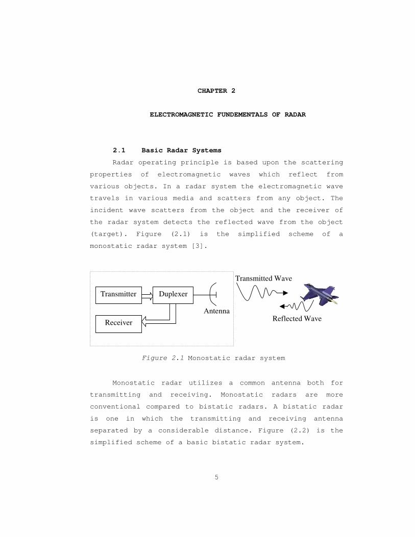
2.1 Basic Radar Systems
Radar operating principle is based upon the scattering
properties of electromagnetic waves which reflect from
various objects. In a radar system the electromagnetic wave
travels in various media and scatters from any object. The
incident wave scatters from the object and the receiver of
the radar system detects the reflected wave from the object
(target). Figure (2.1) is the simplified scheme of a
monostatic radar system [3].
Monostatic radar utilizes a common antenna both for
transmitting and receiving. Monostatic radars are more
conventional compared to bistatic radars. A bistatic radar
is one in which the transmitting and receiving antenna
separated by a considerable distance. Figure (2.2) is the
simplified scheme of a basic bistatic radar system.
Transmitter
Receiver
Duplexer
Antenna
Transmitted Wave
Reflected Wave
Figure 2.1 Monostatic radar system

6
The radar measurements for the bistatic radars are much more
complicated and difficult to accomplish when compared to
conventional monostatic radars.
2.2 Radar Equation
The most important aspect of radar is the radar
equation. Radar equation includes all relation between the
transmitted and reflected power. The most general case of
the radar range equation is for the bistatic radar range
equation, that is:
(2.2)
where;
Pr = reflected power at the receiver antenna site,
Pt = transmitted power from the transmitter antenna,
Gt = gain of the transmitting antenna,
Gr = gain of the receiving antenna,
� = radar cross section,
� = wavelength of the signal,
Rt = distance from target to transmitting antenna,
Rr = distance from target to receiving antenna.
Transmitter
Transmitted Wave Reflected Wave
TransmittingAntenna
ReceivingAntenna
Figure 2.2 Bistatic radar system
Receiver
πλ
ππ=
4
4
4
2
22r
rt
ttr
G
R
�
R
GPP

7
Equation (2.2) does not include polarization and reflection
losses. We can divide the radar range equation into smaller
pieces so that we can understand the whole equation. Power
flux density incident on the target is
(2.3)
Gain of the antenna (G) is defined as the ratio of the
intensity, in given direction, to the radiation intensity
that would be obtained if the power accepted by the antenna
were radiated isotropically. Another sub equation;
(2.4)
defines the isotropically scattered power density at the
position of the receiving antenna. Radar cross section of
the target is �. The final part of the equation
(2.5)
defines the effective area of the receiving antenna.
Effective area represents the amount of the physical area of
an antenna that serves as an electrical antenna.
Radar range equation constructs the fundamentals of
the radar system principles. Equation (2.1) has given for a
bistatic radar system (Figure 2.1) which the transmitting
and receiving antennas are located at different locations.
For monostatic radar systems (Figure 2.2) which one antenna
is used for both transmitting and receiving purposes, the
radar range equation can be written as
(2.6)
24 t
tt R
GP
π
24 rR
�
π
πλ4
2rG
( ) 43
222
22 44
4
4 R
�GPG
R
�
R
GPP ttr π
λ=
πλ
ππ=

8
where Rt and Rr is equal to each other and represented by R.
Receiving and transmitting antennas are the same so the
distance from receiving antenna to target (Rr) is equal to
transmitting antenna to target (Rt). Equation (2.6)
expresses the power received from a target at distance R and
whose RCS is �, the operating wavelength is � and the gain
of the antenna is G. In this simple form of radar equation
losses that occurs from the radar system are not included.
In actual radar systems some of these losses are very real
and cannot be ignored.
2.3 Radar Cross Section
In radar terminology another important property of the
targets is the radar cross section, i.e. � in Equation
(2.4). Radar cross section (�) or RCS of a target is defined
by as the area intercepting that amount of power which, when
scattered isotropically, produces at the receiver a density
which is equal to that scattered by the actual target [4].
RCS is Table 2.1 RCSs of some objects at microwave
frequencies
Object Typical RCS 2
Pickup Truck 200
Automobile 100
Large bomber or jet airliner 40
Medium bomber 20
Large fighter aircraft 6
Small fighter aircraft 2
Human being 1
Conventional winged missile 0,5
Bird 0,01

9
used to determine the scattering characteristics of a
target. RCS of a target depends on the shape, size,
material, properties of the target and the frequency,
polarization and angle of arrival of the incident wave. The
unit of RCS of a three dimensional target is square meters.
Table (2.1) gives RCSs of some objects.
2.4 Common Types of Radar
2.4.1 Pulse Radar
Pulse radar is the common radar type used today. The
transmitted waveform is a train of narrow rectangular pulses
modulating a sinewave carrier. The transmitter is turned on
and off to generate repetitive train of pulses. Peak power
and duration of the pulses and pulse repetitions frequency
(prf) changes regarding to functionality of the radar. After
a pulse is transmitted, radar listens for the echoes from
the targets until the next pulse transmitted. The distance
of the target is determined by the amount of time
transmitted signal is traveled from antenna to object of
interest (target) and back from object to the antenna.
Since electromagnetic energy propagates at the speed
of light c = 2.99795 x 10 8 m/s, the range R is
(2.7)
TR is the total time elapsed between the transmission of the
wave and receiving the reflected wave from the target. In
Equation (2.7) division by 2 comes from the two way
propagation of the wave. Figure (2.3) show a simplified
diagram of a pulse radar system.
2
RcTR =

10
When the distance of the target is so long the
reflected wave can be received after the second pulse
transmitted so ambiguities may occur. The maximum
unambiguous distance is related to pulse repetition
frequency (fp) and given by equation (2.8). Higher pulse
repetition interval results longer unambiguous distance.
Range ambiguities can be avoided by lowering the pulse
repetition frequency and this means a low sampling rate.
Equation (2.8) is applicable for monostatic pulse
radars which have a common antenna used for transmitting and
receiving the signal.
(2.8)
The very first application of range determination by
pulsed signals was in 1925 by Breit and Tuve for measuring
the height of ionosphere [5].
The maximum distance Rmax of the pulsed radar is
directly proportional to pulse repetition interval.
Increasing the pulse repetition interval will increase the
Figure 2.3 Pulse radar system
Duplexer Transmitter Pulse
Modulator
Low Noise Amplifier Mixer
Local Oscillator
IF Amplifier OUTPUT
p
unambf
cR
2=

11
maximum distance of the radar system. Pulse repetition
period is determined essentially by the distance of the
expected targets.
(2.9)
A pulse radar that extracts the doppler frequency
shift for the detection of the moving targets it’s called a
pulse doppler radar.
2.4.2 Continuous Wave (CW) Radar
Continuous wave radars transmit a signal which
oscillates with a frequency of f0. Some of the transmitted
signal reflects from the existing target and reflected
signal collected by the receiving antenna. If the target is
in motion relative to the radar a doppler shift in the
frequency of the received signal will occur. If this is the
case the frequency of the received signal will be f0 ± fd.
If the distance from target to radar is decreasing (a
closing target) the oscillation frequency f0 will increase
by fd, otherwise if the distance is increasing (a receding
target) the oscillation frequency will decrease by fd. A
simplified diagram of the continuous wave radar is given in
Figure (2.4).
CW Transmitter
(f0)
Detector (Mixer) Indicator
Beat Frequency Amplifier
Figure 2.4 CW radar system
f0
f0 f0 ± fd
fd fd
f0
f0 ± fd
2=max
pcTR

12
This type of radar is commonly used for traffic
regulation. The speed indicator used by the policemen is a
kind of CW radar. The frequency shift fd is proportional to
oscillation frequency f0 and the relative velocity of the
target �r.
(2.10)
The graph of Doppler frequency as a function of oscillation
frequency and some relative target velocities calculated
using MATLAB 6.5 is given in Appendix B. An interesting
example of the CW radar is the proximity fuze widely used
during World War II. This fuze is one of the first examples
of the proximity fuzes which operate by the principles of
radar.
2.4.3 Frequency Modulated Continuous Wave (FMCW)
Radar
Frequency Modulated Continuous Wave (FMCW) radar is a
kind of continuous wave radar. Continuous wave radars are
unable to measure the distance between radar and target. To
measure the distance a sort of timing signal must be applied
to the continuous wave carrier. In the FMCW radar the timing
mark can be achieved by frequency modulating the continuous
wave carrier. The changing frequency acts as a time marker
and the elapsed time between transmission and the receiving
the reflected wave can be calculated from the difference in
frequency of the reflected signal and the transmitter.
Another advantage of the FMCW radar system is simplicity of
design when compared to a pulsed radar system. Block diagram
of a typical FMCW radar system may be seen in Figure (2.5).
02f
cfdr
×=ν

13
In FMCW radar systems the common frequency source is a
voltage controlled oscillator (VCO). The modulation
frequency cannot increase continually and must be periodic,
thus VCO is usually controlled by a sawtooth wave shape
generator. When the VCO is controlled by sawtooth wave shape
generator the characteristics of the modulated signal may be
seen in Figure (2.6). In Figure (2.6);
fm = 1 / Tm = Modulation frequency,
fmax – fmin = �f = Frequency deviation,
Td = Delay time.
The frequency difference between the transmitted signal and
the received signal indicates the distance between radar and
the target. This frequency is the major identifier for
distance measurement and called the beat frequency (fb). The
beat frequency fb, is the indicator of the distance between
radar and target. For amplitude fluctuations the beat
frequency is amplified by a low frequency amplifier and then
limited by a limiter. The distance R can be calculated from
Equation (2.11).
FM Transmitter
Modulator
Mixer Amplifier Limiter Frequency Counter
Indicator
Reference Signal
Receiving antenna
Figure 2.5 FMCW radar system
Transmitting antenna

14
In Equation (2.11), fm is the modulation frequency and c is
the speed of light where �f is the deviation of the
modulation frequency which is the difference between the
maximum and the minimum frequency of the transmitted signal.
(2.11)
The greater the deviation of the transmitted signal in a
given time interval, the more accurate the transit time (Td)
can be measured and this result a greater transmitted
spectrum. Speed of light, modulation frequency (fm) and the
deviation of the modulation frequency (�f) is assumed to be
constant, thus the distance from radar to the target is a
function of the beat frequency (fb). For some different
values of frequency deviation and modulation frequency, beat
frequency versus distance from radar to target is given in
Figure (2.7) and Figure (2.8).
Td
Tm
fmax fmin
�f fb
f
t
Frequency of transmitted signal Frequency of received signal
Figure 2.6 Frequency variation of transmitted and received signal
ff
cfR
m
b
∆=4

15
0 100 200 300 400 500 600 700 800 900 10000
50
100
150
200
250
300
350
400
450
0 100 200 300 400 500 600 700 800 900 10000
200
400
600
800
1000
1200
1400
Distance (m.)
Beat Frequency (KHz)
Figure 2.7 Beat frequency variation (fm = 1 KHz)
Beat Frequency (KHz)
Distance (m.)
Figure 2.8 Beat frequency variation (fm = 3 KHz)
�f = 10 MHz
�f = 15 MHz
�f = 20 MHz
�f = 25 MHz
�f = 30 MHz
�f = 10 MHz
�f = 15 MHz
�f = 20 MHz
�f = 25 MHz
�f = 30 MHz

16
The choice of frequency modulation and modulation
deviation is determined by the ranging sensitivity, K =
4fm�f / c (Hz/m). For example if a VCO is linearly modulated
at a rate of 10 KHz per over a range of 1 GHz the beat
frequency of the FMCW system will be 133 KHz per meter of
range. A wider range of frequencies swept by the modulation
waveform and a higher frequency of the modulating waveform
will yield more accurate measurement of the range
information. Another consideration for beat frequency and
doppler shift must be made if the radar or the target is in
motion. A frequency shift by doppler effect will be
superimposed on the beat note and an erroneous range
measurement results. The doppler frequency shift will causes
the beat frequency echo signal to be shifted up or down by
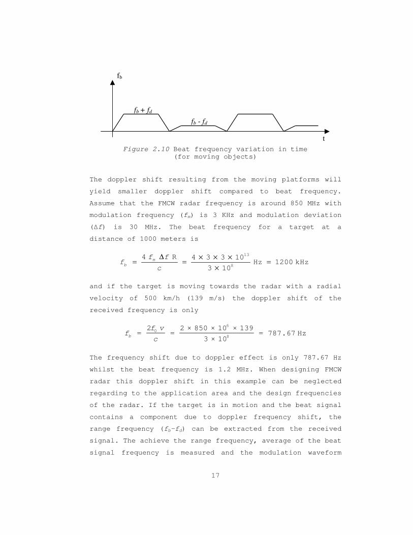
doppler shift (fd). Figure (2.9) illustrates the beat
frequency time plot of the echo signal. On the time plot of
the beat frequency the doppler shift can be seen in Figure
(2.10).
fb
t Figure 2.9 Beat frequency variation in time
(for stationary objects)
fb
Tm
17
The doppler shift resulting from the moving platforms will
yield smaller doppler shift compared to beat frequency.
Assume that the FMCW radar frequency is around 850 MHz with
modulation frequency (fm) is 3 KHz and modulation deviation
(�f) is 30 MHz. The beat frequency for a target at a
distance of 1000 meters is
and if the target is moving towards the radar with a radial
velocity of 500 km/h (139 m/s) the doppler shift of the
received frequency is only
The frequency shift due to doppler effect is only 787.67 Hz
whilst the beat frequency is 1.2 MHz. When designing FMCW
radar this doppler shift in this example can be neglected
regarding to the application area and the design frequencies
of the radar. If the target is in motion and the beat signal
contains a component due to doppler frequency shift, the
range frequency (fb-fd) can be extracted from the received
signal. The achieve the range frequency, average of the beat
signal frequency is measured and the modulation waveform
fb
t Figure 2.10 Beat frequency variation in time
(for moving objects)
fb + fd
fb - fd
kHz1200Hz103
10334R48
13
=×
×××=∆
=c
fff mb
Hz67.787=10×3
139×10×850×2=
2=
8
60
c
vffb

18
must have equal upsweep and downsweep regarding the doppler
frequency shift. Also when the average of the beat frequency
is measured for one cycle of the modulation frequency, the
doppler effect will be cancelled.
2.4.4 Pulse Modulated FMCW Radar
Another type of the FMCW radar is the pulse modulated
FMCW radar. In the pulse modulated FMCW radar, the
transmitter transmits the signal only for a limited time
interval and then the receiver listen for the echoes of the
transmitted signal.
In pulse modulated FMCW radar the transmitted signal
reflects back from the target and the frequency of the
received signal compared with the modulator frequency. Beat
frequency is the difference between the modulator frequency
and the received signal. The modulator frequency acts as a
time marker as in the FMCW radar. Except from the FMCW radar
the pulse modulated radar has blind range. Blind range
occurs when the signal pulse is transmitted because the
receiver is blocked within the time period of transmission.
f
t
Modulation waveshape
Figure 2.11 Pulse modulated FMCW radar frequency variation
Transmitted signal (pulse)
Received signal (echo of the pulsed signal)
Td
fmax
fmin

19
Despite the range limitation of the pulse radar that is
limited to a value depending on the unambiguous distance
(Runamb) given in Equation (2.8), the pulse modulated FMCW
does not have range ambiguities depending on the pulse
repetition frequency. Because pulse modulated FMCW radar
utilizes the beat frequency measurement instead of time
delay measurement. The blind range (Rp) is calculated from
Equation (2.12) and the multiples of the blind range are
also blind. Tp is the pulse interval.
(2.12)
The blind range width is dependant to the pulse width of the
transmitted pulse. It is advantageous to reduce the pulse
width as short as possible to achieve the minimal blind
range width. Actually, FMCW radar also has range ambiguities
and maximum range depending to the modulation frequency. The
maximum range (Rmax) is equal to the distance traveled by a
wave (velocity = speed of light) within the half period of
the frequency modulation. For example, if the modulation
frequency is 1 KHz then the maximum unambiguous distance is
Tm/2 times the speed of light. If this is the case maximum
unambiguous distance is 149.897 kilometers. If the distance
exceeds the maximum distance (2Rmax>R>Rmax) the calculated
beat frequency peak will be
(2.13)
Equation (2.13) results from the downsweeping of the
triangular waveform. When the distance (R) is longer from
the maximum distance (Rmax) the modulation frequency slope
changes its sign from positive to negative or vice versa
after the delay time (td) corresponding to distance of the
( )c
RRfff maxmb
-××∆××=
24
2p
p
cTR =

20
target. This theoretical result does not occur because the
maximum distance is usually much longer from the target
distance at the FMCW radar applications. If the modulation
frequency fm is equal to 3 KHz, the maximum distance Rmax
will be 100 kilometers. And if the target distance is longer
than 100 km then we can easily change the modulation
frequency to a higher value then 3 KHz and these situations
are usually well defined at the design phase.
21
CHAPTER 3
SURFACE ACOUSTIC WAVE (SAW) DEVICES
3.1 Introduction to SAW Devices
Integrated Circuits (IC) are small and contain many
elements up to 108. At the same time it is important that
ICs contain only transistors, diodes, resistors and
capacitors. Practically inductive elements cannot be
integrated in monolithic ICs.
With the development of ICs, the problem of
miniaturization of filters, delay lines and other components
that included inductive elements appeared. As a result of
search of ways to miniaturize mentioned components, surface
acoustic wave (SAW) devices were created.
The fundamentals of this technique lie in the
discovery of the piezoelectricity by the brother Curie in
1880 and of the surface acoustic waves in 1885 which is the
basis of the SAW devices by the famous English scientist
Lord Rayleigh. Piezoelectricity is a coupling between
elastic deformation and electric polarization which exists
in certain crystals such as quartz. Surface waves are
piezoelectric microwaves which can be propagated over the
surface of these crystals at a velocity of the order 3500
m/s. After the studies of Rayleigh, the surface acoustic
waves are first observed at the beginning of the twentieth
century that an earthquake could be detected at a great
distance by two tremors corresponding to the modes of volume
propagation, transverse and longitudinal modes and one
tremor corresponds to surface propagation on the earth’s

22
crust in the form of acoustic waves which arrived later from
the first two modes.
The application of SAW begins from 1965 with the
invention of an effective piezoelectric transducer, in the
form of an Interdigital Comb, by White and Walter [6]. This
transducer implemented on a substrate by photolithographic
methods using the means of microelectronic techniques.
Acoustic surface waves nowadays called Rayleigh waves are
useful because the propagation of these waves is very much
smaller compared to the velocity of the electromagnetic
waves. So the associated components with the surface
acoustic waves are smaller too. The very first application
of the SAW devices is in the area of military which uses
pulse compression in modern radar and sonar in 1965-1970.
Today SAW devices have many applications, every modern
television have at least one receiver with a SAW filter and
many of the telecommunication system, satellite systems, and
smaller radar systems utilizes the high performance SAW
filter techniques. The nonlinear properties of the SAW
materials form the basis of the frequency multiplication and
the systems uses oscillator with the low frequency quartz
crystal followed by a frequency multiplier chain replaced
with high frequency SAW precise oscillators.
The SAW devices have may advantages such as low
marginal cost, excellent reproducibility, electrical and
mechanical robustness. The large frequency range of these
devices and the flexibility of the SAW oscillator by
adapting the peak voltage to the desired function to utilize
an oscillator tunable over a wide frequency range, a
frequency modulated oscillator or a very stable frequency
generator, adds another advantage to these devices. And the
interaction of the acoustic wave with an external wave such
as a light wave, a wave in the space charge associated with

23
the movements of electrons or a magnetic wave results the
large application area of the SAW devices.
3.2 Theory of SAW Devices
The design goal of the filter is to select material
for the waveguide, determine the main filter dimensions, and
examine its frequency characteristics correspondence to the
given specification.
The main electrical parameters (central frequency of
the pass-band f0 and bandwidth �F of the filter) are
presented as initial data for design calculations.
The goal of the calculations is to select material for
the waveguide, determine main dimensions of filter elements
and examine its frequency characteristics correspondence to
the given specification.
Interdigital Transducers (IDTs) are the main elements
of a SAW filter consisting of input transducer, waveguide
and output transducer. An IDT is shown in Figure (3.1). Most
of the SAW devices use materials like quartz, lithium
niobate (LiNbO3) and lithium tantalite (LiTaO3). Strong
electromechanical coupling factors (k2) makes these crystals
preferable but these crystals are very temperature sensitive
so they are excluded from certain functions. The double
oxide of bismuth and germanium (Bi12GeO20) has a SAW velocity
which is approximately half of the SAW velocities of the
other crystals given in Table (3.1). For the realization of
long delay lines with Bi12GeO20 will be preferable compared
to some other crystals. Gallium arsenide (GaAs) has a double
advantage of being piezoelectric and semiconducting. By the
piezoelectric and the semiconducting properties of the
gallium arsenide the realization of integrated acoustic and
microelectronic device both on the same substrate allowed.

24
Piezoelectric coupling factor (k2) is a parameter which
measures the reduction in velocity. When the surface is
isolated and free the velocity of the surface wave velocity
is denoted as ν�, if surface is short-circuited, the
velocity of propagation reduces to a value ν0. The reduction
of the velocity is in the order of 0.1% to 5% and is very
precise. The piezoelectric coupling factor (k2) can be
formulated by equation (3.1).
(3.1)
Absorber Absorber
Input Transducer
Output Transducer
Waveguide
Figure 3.1 SAW filter
Table 3.1 Parameters of piezoelectric materials
Crystal SAW velocity νs (m/s)
Coupling coefficient
k2
(%)
Relative dielectric
permittivity
rε
Quartz 3158 0.16 4.5 LiNbO3 3490 5 46 Bi12GeO20 1681 1.4 40 GaAs 2863 0.09 11 LiTaO3 3230 0.9 47 AlPO4 2736 0.56 6.1
2
20
22
∞
∞
νν−ν=k

25
There are several modes of propagation. The most
commonly used modes are the Rayleigh Modes. There are other
modes called pseudo-modes which are propagated with
attenuation and Bluestein-Gulyaev modes and Surface Skimming
Bulk Waves (SSBW) as well. We shall discuss only the
Rayleigh modes because the other modes usually concerns
oscillator applications and can be neglected.
Surface-wave delay line is a lossless line with the
real characteristic impedance
(3.2)
The impedance of a capacitance deposed on a piezoelectric
substrate is given by
(3.3)
C is the electrostatic capacitance of the interdigital
transducer (IDT). The capacitance can be expressed by
Equation (3.4).
(3.4)
In equation (3.4), ε is the permittivity and W is the
useful length of the electrodes. Which permittivity involved
is actually depends on the mode of propagation. For Rayleigh
type modes permittivity is given in two forms. One is the
“high frequency” and the other is “low frequency”
permittivity and denoted by respectively HFε and LFε . For
the coupling frequency k2 we take the permittivity
(3.5)
ωε=
W
kRc
2
( ) ( )ω+ω
=ω 0
1R
jCjZ
WC ε=2
1
( ) eLF k ε+−ε≈ε 21

26
where eε is the permittivity of the external medium which in
general is air or vacuum.
The radiation resistance R0 varies slowly with
frequency and given by:
(3.6)
where � is the coefficient which characterize the geometry
of the capacitances and particularly the metallization
ratio. The value of this coefficient is usually between 0.6
and 0.8. For a regular interdigital comb consisting of N+1
identical electrode with constant spacing d and constant
aperture W, the impedance can be given by equation (3.7).
(3.7)
The formula given by equation (3.7) is one of the most used
because of its simplicity. In equation (3.7) the variable x
is equal to ( ) 00 2ωω−ωπ N .
In the simplest case the filter contains two identical
rectangular IDTs, a transmitter and a receiver. The SAW
filter is not only a filter satisfying the prescribed
specifications, indeed is a delay line. A wide band filter
cannot be designed by using arbitrary materials. The
theoretical relation of the bandwidth given by:
(3.8)
where �F is the bandwidth and f0 is the center frequency. In
practice, it is very difficult to construct delay lines of
relative bandwidth noticeably larger than k. Table (3.2)
illustrates this limitation for commonly used materials.
WC
k.
WC
kR
ε≈
εα≈
222
0
412
( ) ��
���
� −+��
�
�+ω
=ω2
2
02
221
x
xxsinj
x
xsinR
jNCZ
kf
F ≈∆
0

27
LK
a
Ld
W
b∆
For the simplest SAW filter containing two identical
IDTs which is shown in Figure (3.2), design calculations
sequence can be like this [7]:
Table 3.2 Maximum practical bandwidth for different piezoelectric materials
Crystal k Bandwidth
(%)
Quartz 0.4 4 LiNbO3 2.24 25 Bi12GeO20 1.18 10 GaAs 0.3 3 LiTaO3 0.95 10 AlPO4 0.75 8
Figure 3.2 Interdigital comb

28
1. Number of IDT fingers is calculated using the
formula:
(3.8)
Here � is a coefficient between 0.6 and 0.8 which defines
the metallization.
2. The efficiency of an IDT is maximal when N is close
to the optimal number Nopt, dependent on substrate material:
(3.9)
Here k2 is piezoelectric coupling coefficient (see Table
3.1).
3. If N � Nopt, the deviation from the optimum is
characterized by a coefficient P:
(3.10)
4. The step � of IDT fingers must satisfy condition in
Equation (3.11). (νs is the SAW velocity)
(3.11)
The width d of the finger usually is half a step: 2∆=d .
5. The overlap of IDT fingers must be at least:
(3.12)
where L is the distance between the input and output
transducers, �s is SAW wavelength. The distance L is
recommended to be 8–10 mm.
FfN ∆α= 02
24kN opt π=
( )2NNP opt=
smin LW λ=
02� fs=∆

29
6. The IDT length is given by:
(3.13)
7. The substrate length must be:
(3.14)
where l is the distance between IDT and substrate end.
8. The substrate width is given by:
(3.15)
Selection of filter dimensions and other parameters
can be followed by the calculations of its electrical
parameters and characteristics.
9. Reflection coefficient B1 of SAW from the IDT,
transition coefficient B2 and IDT attenuation B3 (in
decibels) are given by:
(3.16)
(3.17)
(3.18)
10. SAW filter attenuation is given by:
(3.19)
11. Level of distortion signals caused by reflections:
(3.20)
2∆−∆= NLk
( )lLLb k ++= 2
( )lWa +∆+= 2
( )[ ]21 1110 PlogB +−=
( )[ ]23 1210 PPlogB +−=
( )[ ]222 110 PPlogB +−=
32BB =
32BBd =

30
12. Static capacitance of an IDT is given by:
(3.21)
where C1 is capacitance of a finger given by:
(3.22)
Here εr is relative dielectric permittivity of the substrate
material, s is ratio, ∆d .
13. Radiation resistance Rr of the IDT at f = f0 is
given by:
(3.23)
14. To avoid capacitive component of the input
resistance of the IDT an inductive element is used in series
with the IDT [8]. Its inductance can be find using formula:
(3.24)
15. The transfer function of the SAW filter is given
by:
. (3.25)
Here ( )ωjK 1 is the transfer function of the SAW filter input
circuit:
(3.26)
where
0PRR = ,
210 WNCC =
( )( )3720815612 21 .s.s.C r ++ε+≈
( ) WCfkfRR mr 1022
00 2 π==
02041 CfL π=
( ) ( )( ) ( ) ( ) ( )
( )04
432
01
1
ωω
ωωωω
=ωjK
jKjKjK
jK
jKjK F
( )ZLjR
ZjK
+ω+=ω1

31
( ) ( ) 01 CjfjXfRZ aa ω++= which is given in equation
(3.7),
( ) ( )20 xxsinRfRa = ,
( ) ( ) 20 222 xxxsinRfXa −= ,
( ) 00 2fffNx −π= .
( )ωjK 2 and ( )ωjK3 are transfer functions of the input and
output IDTs:
(3.27)
( )ωjK 4 is the transfer function of the SAW filter
output circuit, consisting of Z, L and load resistance R:
(3.28)
16. When the reflected wave is taken into account the
transfer function of the SAW filter is given by:
(3.29)
where Ltν is the delay time given by ( ) pKL LLt ν+=ν and Kp
is transfer coefficient corresponding to attenuation Bd.
The choice of material is important for SAW
technology. Any arbitrary material is vulnerable to satisfy
the desired characteristics for the filter [9]. Figure (3.3)
illustrates some materials and technology associated with
SAW delay lines (filters) and must be treated with caution.
The performance of the present SAW filters and foreseeable
limits for some characteristics are given in Table (3.3)
( ) ( )x
xsinjKjK =ω=ω 32
( ) ( )LjZRRjK ω++=ω4
( ) ( ) ( )LpF texpKjKjK νΣ ω−+ω=ω 2

32
LiNbO3
Quartz
Resonators
��/� (%)
f0
30 MHz 100 MHz 300 MHz 1 GHz 1 GHz
0.01
0.1
1
3
10
30
Figure 3.3 Choices of materials and of technology for different characteristics of filters
Table 3.3 Performance of SAW filters
Present Limits
Typical Values Foreseeable
Limits
Central Frequency
10 MHz – 4.4 GHz
10 MHz – 2 GHz
6 GHz
Bandwidth 50 KHz - 0.7 f0
100 KHz – 0.5 f0
0.8 f0
Insertion Loss (min)
2 dB 3-20 dB 1 dB
Shape Factor (min)
1.2 1.5 1.2
Transition Band (min)
50 KHz 100 KHz 20 KHz
Rejection 60 dB 50 dB 70 dB
Phase Difference/ Linear Phase
± 1� ± 2� ± 0.5�
Ripples 0.01 dB 0.05 - 0.5 dB 0.01 dB

33
CHAPTER 4
THEORY AND DESIGN
4.1 Introduction
Designing a pulse FMCW radar is a complicated task
which involves many variables concerning maximum detectable
range, relative velocity, noise considerations, necessary
transmitter power and the final interpretation of the
received information. Of course, some of these variables are
constrains regarding to the application requirements of the
system and some of the variables are to be defined after the
design.
The pulse FMCW radar system will be used to measure
the distance of the target in a maximum range of 1000
meters. The radar must be designed to have the maximum
detectable range longer than 1000 meters. Target in the
system is an infinite obstacle and stationary. Small size
and lightweight is also the primary requirements.
Throughout this chapter some design issues are given
and a simplified test technique for the radar system using
surface acoustic wave (SAW) devices is given as well. The
block diagram of the FMCW radar has already been given in
Figure (2.5). Block diagram for pulse FMCW radar is given in
Figure (4.1).

34
4.2 Back Scattering From Target
The system will be able to measure the distance of the
targets within 1000 meters range. The target is the earth’s
surface. The radar itself can rotate both on the and
axes of the spherical coordinate system but rotation is
limited to 90 degrees on the axis. However, ground surface
extends to infinity in dimension compared to the
illumination area of the radar. Thus, rotation on the axis
does not affect the illuminated area of the target by radar
which has a uniform beamwidth on the and axes. Radar and
target can be seen in the Figure (4.2).
Frequency Modulator
Power Amplifier
Circulator
DSP Band Pass Filtering and Beat Frequency Amplifying
fpass= fbmin - fbmax
Antenna
Mixer
Directional Coupler
Data Acquisition Systems (Computer, Display, VTR)
Figure 4.1 Pulse FMCW radar block diagram
Band Pass Filtering and
LNA
Voltage Controlled Oscillator
(VCO)
Amplifier
RF LO
IF
Switch

35
The azimuth beamwidth along R is denoted by �B and the
azimuth beamwidths along the cuts 0+B/2 and 0-B/2 are �1
and �2, also assumed to be equal (�1 = �2 = B). To calculate
the power related issues we must define the illuminated area
(�S) with respect to angle of incidence (), beamwidth of
the antenna (B) and distance from target (d). The
illuminated area by the radar (�S) can be calculated from
Equation (4.1).
(4.1)
Received power at the antenna port (�Pr), by the reflections
of the transmitted signal from the illuminated surface of
the target (�S), can be expressed by Equation (4.2)
(4.2)
d
R
�0
Radar Target
R1
R2
�0+�B/2 �0-�B/2
Figure 4.2 Angle of incidence
radradBrad
B
rad
cos
dRR
cos
RS θ∆
θΦ≈+Φ
θθ∆=∆
2
221
2
( )( ) 43
020
2
π4∆σλθ
=∆R
SGPP
radt
r

36
Radar Cross Section (RCS) of the target can be approximated
as an exponential function given in Equation (4.4) [10]
(4.3)
(4.4)
�o is called the radar land reflectivity. o is usually
expressed in dB(m2/m2). o has a strong dependency to the
type of the surface (roughness) especially for the lower
microwave frequencies and vary between -3 dB to -29 dB for
grazing angles 7 to 70o. The median value is -14 dB which is
the average of the various resulted from experiment. For the
grazing angles greater than 65o, �o so does �o rapidly
increases to a value of 0 to 15 dB (m2/m2). The maximum
values are dominant for the urban areas. Land reflectivity
depends on the type of surface, frequency and angle of
incidence (). Land reflectivity is maximum for angle of
Figure 4.3 Illuminated area
d
�
Radar Target
R1
R2
��
�S R��
�
�R
( ) ( ) ScosSRCS ∆θθγ=∆σ= 00
( ) ( ) ( )( )
10θΨ
0θ20− 10=θγ −114−=θΨ .e

37
incidence = 0o and falls off rapidly as the increases
[10].
The gain pattern of the antenna with gain G can be
given as
(4.5)
( )θnf is the normalized antenna pattern in elevation plane
and can be approximated by a Gaussian function normalized to
0 dB. Normalized antenna pattern equals to -3 dB in Equation
[4.6] when is equal to half of the beamwidth.
(4.6)
-200 -150 -100 -50 0 50 100 150 200-15
-10
-5
0
( ) ( )θ=θ 2n
rad GfG
( ) ( ) dB/.f.
B.
n
510
51 θθ−θ×2×150−=θ
Figure 4.4 Normalized antenna field pattern
� (Degrees)
fn(�)(dB)

38
Substituting Equation (4.1), (4.3), (4.5) in the
Equation (4.2), the received echo power at the antenna port
(�Pr) can be found as in Equation (4.7).
(4.7)
Replacing R, and rad ;
(4.8)
we finally get Equation (4.9).
(4.9)
θ∆∆ rP is the angular distribution of the received echo power
reflected from the target. Power received from an angle of
incidence from an angular width of � is;
(4.10)
where;
(4.11)
(4.12)
4.3 Echo Power Angular Distribution
Angular distribution (density) of the received echo
signal at the antenna of the system is plotted using
Equation (4.10), changing from -10o to 70o for different Q
values corresponding to distance of 100, 500 and 1000
meters. The MATLAB (version 6.5) “m files” necessary to plot
the angular distribution are given in Appendix C. Two source
( ) ( )( ) ( )θπ
θ∆Φθγλθ=∆
cosR
dfGPP
radradBnt
r 43
20
20
42
4
( ) BradB
rad ,,cos
dR Φπ=Φθπ=θ
θ=
180180
( )( ) ( ) ( ) ( )θθγθπ
πΦλ
=θ∆
∆ 20
42
23
20
2
1804
cosfd
GPPn
Btr
( ) ( )��θ∆+θ
θ
θ∆+θ
θ
θ′θ′=θ=θ∆+θθ∆ d.YQd.dP,P rr
( )
2
23
20
2
��
�
�
180π
π4Φλ
=d
GPQ Bt
( ) ( ) ( ) ( )θθγθ=θ 20
4 cosfY n

39
codes (m files) for MATLAB in Appendix C, calculates the
angular distribution of the received echo for � = 1o using
two different techniques and results are very close to each
other.
By using recursive adaptive Simpson quadrature in the
m file named “Pr.m”, integral is calculated with an error of
less than e-6. For m file “directPr.m” line integral from
to +� did not evaluated and � is taken directly as 1 and
Pr calculated for . Figure (4.5) is the angular
distribution of the received echo power (dBm) in �=1o
angular width.
Frequency range of the system is between 800-900 MHz
and for the calculations of the angular distribution of the
received echo power, center frequency is taken as 850 MHz.
From Figure (4.5) we can conclude the received echo signal
will be maximum -50 dBm and the minimum received signal will
be approximately -100 dBm at grazing angle of 30 degrees.
The rain and atmospheric attenuations can be neglected at
this frequency [1]. The output power transmitted at the
antenna (Pt) is taken as 30 dBm (1W) and the elevation and
azimuth beamwidths of the antenna (B,�B) are taken as both
80o and the gain of the antenna (G) is taken as 8 dB.

40
-10 0 10 20 30 40 50 60 70-105
-100
-95
-90
-85
-80
-75
-70
-65
-60
-55
4.3 Echo Power Spectrum
Echo power spectrum of the radar determined by
replacing the angular information with frequency
information, which can be derived using Equation (2.11).
(4.13)
K is the ranging sensitivity in Hz/m.
�R is the change in the radial distance when the angle
of incidence is change by �. From Figure (4.3);
(4.14)
(4.15)
� (degrees)
d= 1000m, Q=6.07x10⁻⁸
d= 100m, Q=6.07x10⁻⁶
d= 500m, Q=2.43x10⁻⁷
Figure 4.5 Angular distribution of the echo power at the antenna port
�Pr,dBm (��=1o), �o=30o
c
ffK,R.Kf m
b
∆4==
( ) ( )( ) ( )
brad f
d.Kcos,
.R
R
cos
sintan =θ
θ∆∆=
θθ=θ
K
fR
K
fR bb �
� = =

41
(4.16)
(4.17)
(4.18)
Substituting �rad in Equation (4.9) we get;
(4.19)
For the values of we can use the inverse cosine function
which is shown in Equation (4.20).
(4.20)
The received echo power (dBm) is calculated and
plotted using MATLAB. “beatvariation.m” given in Appendix C
is the source code for Figure (4.6) and (4.7). Center
frequency is taken as 850 MHz, and K is equal to 1334 and
125 Hz/m. To calculate the echo power �Pr is integrated over
from 1 to 2 .
(4.21)
(4.22)
(4.23)
( )( ) ( )
�
�
��
sinf
f.d.K
sinR
cosR
tanR
R
b
brad
2===
( ) ( )2
2���
�
�−1=−1=
bf
d.Kcossin
( )22 −1=
bb
brad
fd.Kf
f.d.K ��
( ) ( ) ( )( )24
3
04
−1=
bb
n
b
r
fd.Kf
d.KQf
f
P
�
�
���
�
���
�
�
π=θ −
bf
d.Kcos 1180
���
�
�
2∆−��
�
�π
180=θ 1−1
bb ff
d.Kcos
���
�
�
2∆+��
�
�π
180=θ 1−2
bb ff
d.Kcos
( ) ( )��2
1
2
1
θ
θ
θ
θ2112 θ′θ′=θ=θθ= d.YQd.dP,PP rr

42
Power spectrum for ranging sensitivity (K) equal to
125 Hz/m and �fb=1.172 is given in Figure (4.7).
Echo power spectrum decays rapidly because of the change of
the land surface reflectivity by the angle and the forth
power dependence of the received echo power to the distance
between radar and target.
0 0.5 1 1.5 2 2.5 3
x 106
-140
-130
-120
-110
-100
-90
-80
-70
-60
Figure 4.6 Power spectrum of the echo signal at the antenna port (K=1334 Hz/m)
�Pr,dBm(fb)
fb (Hz)
K=1334 Hz/m �o =30 o �fb=1.172 KHz d=100 m
d=500 m
d=1000 m

43
0 0.5 1 1.5 2 2.5 3
x 106
-180
-160
-140
-120
-100
-80
-60
-40
4.4 Noise Analysis
Flow of charges and holes in the solid state devices
and the thermal vibrations in any microwave component at a
temperature above absolute zero is the cause of the noise.
Noise temperature (T) is the expression of the noise
introduced to the system.
The pulse FMCW radar system will be subjected to two
kinds of noises. One is the phase noise and the other is the
thermal noise. In this section noise analysis of the
receiver of the radar is given. Phase noise (PN) injected to
the system is oriented from the voltage controlled
oscillator (VCO); thermal noise (TN) is oriented from VCO
and from solar, galactic (which are called cosmic noises)
and atmospheric absorption noises. Noise at the receiver
Figure 4.7 Power spectrum of the echo signal at the antenna port (K=125 Hz/m)
�Pr,dBm(fb)
fb (Hz)
K=125 Hz/m �o=30 o
�fb=1.172 KHz
d=100 m
d=500 m
d=1000 m

44
side is the dominant term affecting the maximum range of the
system.
4.4.1 Noise Figure (Noise Factor)
Noise figure (also called noise factor) of a receiver
can be described as a measure of the noise produced by a
practical receiver as compared with the noise of an ideal
receiver. The noise figure (Fn) of a linear network can be
defined as
(4.24)
Sin = available input signal power,
Nin = available input noise power (kT0BnG),
Sout = available output signal power,
Nout = available output noise power.
inout SS is the available gain (G) of the network. Boltzman
constant (k) is equal to 1,38x10⁻²³ J/deg and Bn is the noise
bandwidth of the network. T0 is approximately standard room
temperature of 190o Kelvin (K). Noise figure is commonly
expressed in decibels, that is, 10xlog10(Fn). Noise figure
may also be expressed by;
(4.25)
where �N is the noise introduced by the network itself.
Noise figure of a cascade network is dominated by the
noise figure of the first network. For a cascade network
given in Figure (4.8) the noise figure is given in Equation
(4.26).
It is the first term in Equation (4.26) dominating the
overall noise figure of the cascaded network and the second
network contribute to only 1/G of its noise figure to the
overall system. Thus many practical receiver systems utilize
GBkT
N
NS
NsF
n
out
outout
ininn
0
==
GBkT
NF
n
n
0
∆+1=

45
Low Noise Amplifier (LNA) which as the first stage of the
receiver and the second stage is usually a mixer whose noise
performance usually tends to be poor.
(4.26)
For the receivers, noise considerations play an
important role because it is one of the dominant limitations
limiting the maximum range of the radar. The stages of the
receiver side of the radar are shown in Figure (4.9). The
receiver side consists of an antenna, a circulator,
broadband (100 MHz) filtering and amplifying circuit, RF
mixer whose local oscillator (LO) input is the output of the
VCO and baseband (150 KHz) filtering and beat frequency
amplifying circuit. The output baseband signal is connected
to the Digital Signal Processing (DSP) chip for Fast Fourier
Transform (FFT) to signal processing the beat frequency
signal and switching functions of the radar.
F1 G1
F2 G2
Fn Gn
Fcas G1G2 …Gn
Figure 4.8 Cascaded network noise figure
Ni Nout
Ni Nout
( ) ( ) ( )1−2121
3
1
21
1−++1−+1−+=n
ncas G...GG
F...
GG
F
G
FFF

46
For a network with noise figure Fn and gain G, the
relationship between the input and the output noise can be
found by Equation (4.32). Tn,in is the input noise
temperature and Tn,out is the output noise temperature and F
is the noise figure and G is the gain of the network. Noise
introduced to the system by the network itself �N is given
in Equation (4.25). From Equation (4.25) we get;
(4.27)
(4.28)
Filtering and Beat Frequency Amplifying
Mixer
Filtering and LNA
RF
LO
IF VCO
Signal Processing
Circulator
Antenna
Broadband RF BW=100 MHz
Baseband IF BW=150 KHz
Figure 4.9 Receiver side of the pulse FMCW radar
Switch
( ) nGkBTFN 01−=∆
nout,n kBTN ∆=∆

47
(4.29)
(4.30)
(4.31)
(4.32)
where T0 is 290o K, Bn is the bandwidth of the network, �N is
the noise of the network itself. The noise corresponding to
the output noise temperature can be calculated from Equation
(4.31).
(4.31)
(4.32)
4.4.2 Phase and Thermal Noise from VCO
Phase noise is the phase fluctuations due to random
fluctuations of a signal [11]. The amplitude noise of a VCO
is approximately 20 dB lower than the phase noise. Phase
noise can be modeled by a narrowband FM signal. Output of
the VCO then can be expressed by Equation (4.33).
(4.33)
(4.34)
where � is the modulation index by analogy to modulation
theory, �� is the frequency deviation and ��/�n is the rate
of frequency deviation.
01−=∆ GT)F(T out,n
GTTT in,nout,nout,n +∆=
( ) GTGTFT in,nout,n +1−= 0
( )[ ]GTTFT in,nout,n +1−= 0
nnnn GBT,GBkTN ×10×381== 23−
n
dBm,N
dBm,nGB,
T×10×381
10= 23−
10
( )( )tcostcosVV ncc ωβ+ω= 0
( )n
nnn ,tcosP
ωω∆
=βωβ=

48
Phase and thermal noises of the VCO may be injected to
the receiver IF side via;
a. LO port of the mixer,
b. Leaking from circulator,
c. Reflecting back from antenna,
d. Reflecting back from ground.
In pulse FMCW radar, the pulses are generating by a
transmitter switch (Stx) and there is another switch at the
receiver called receiver switch (Srx). These two switches
are operated reversely. When the radar is in transmission
mode the transmitter switch is closed and receiver switch is
opened, and vice versa. The leaking noise through circulator
(b) and noise reflected from the antenna (c) are prevented
by the reverse operation of the switches. The only noise
from VCO affecting the system is via LO port of the mixer
(a) and reflecting from ground (d).
Conversion Loss (CL) of a mixer is the amount of RF
power to be converted to IF power.
(4.36)
Output of the mixer IF port can be expressed by;
Mixer
LO RF
IF
V0 VE
VCO Antenna
Figure 4.10 Mixer port signals
powerIFavailable
powerRFavailableCL =

49
(4.35)
(4.36)
VE is the echo signal reflected back from target with a
delay of Td. cω′ is the carrier frequency at time t-Td. k is
the mixer constant.
(4.37)
20kV is equal to conversion loss (CL).
If we introduce the thermal noise into Equation (4.36)
we get the total IF output VIF ;
(4.38)
where;
LOin , LO
qn are the in-phase and quadrature noise voltages at
the LO port of the mixer,
Ein , E
qn are the in-phase and quadrature noise voltages at the
RF port of the mixer due to reflection from the ground.
LOin , LO
qn >> Ein , E
qn as the echo from the ground is weighted by
( )[ ]430
22 4 RSG π∆σλ . The LO signal level (V0) is large so,
LOin , LO
qn << V0, thus thermal noise oriented from VCO can be
neglected. We will calculate phase noise in Section (4.4.4).
4.4.3 Antenna Thermal Noise
In previous section we show that the thermal noise of
the VCO is very small compared to the phase noise of the
VCO. It is assumed the thermal noise due to galactic and
( ) ( ) ( )( )[ ]{( ) ( ) ( )( )[ ]}Ednncc
EdnnccEIF
Ttcostcostcos
TtcostcostcosVkV
V
φ−−ωβ+ωβ+ω′+ω
+φ+−ωβ−ωβ+ω′−ω=20
EcIF VVkV ××=
( )( )( )( )[ ]EdncE
ncIF
TtcostcosV
tcostcosVkV
φ−−ωβ+ω′×ωβ+ω×= 0
( )( ) ( ) ( ) ( ) ( )[ ]( )( )[ ] ( ) ( ) ( ) ( ){ }tsintntcostnTtcostcosV
tsintntcostntcostcosVkV
cEqc
EiEdncE
cLOqc
LOincIF
ω−ω+φ−−ωβ+ω′×
ω−ω+ωβ+ω×= 0

50
solar noises (cosmic noise) will be dominant. The leakage
thermal noise from the VCO is eliminated by the switching
configuration. VCO will contribute to overall system noise
by introducing phase noise to the receiver side from the LO
port and due to reflection from ground. Another thermal
noise contributed to the system is due to the cosmic sources
and atmospheric absorption noise.
Atmosphere absorbs certain amount of energy and
reradiates it as noise. While absorbing the energy
attenuation in the energy occurs. Absorbed microwave energy
is equal to the noise power (�N) radiated by itself. Thus;
(4.39)
(4.40)
where Ta is the ambient temperature, Te is the effective
noise temperature (cause of atmospheric absorption noise)
and L is the atmospheric attenuation loss. 1/L is the gain
(Gatm) of the atmosphere. Through passing from atmosphere
some portion of the cosmic noise is absorbed by the
atmosphere and reradiated as cosmic noise. Cosmic noise
temperature (Tb) at the antenna (Tb,ant) can be calculated
from Equation (4.41).
(4.41)
(4.42)
(4.43)
��
�
� 1−1==∆L
BkTGBkTN nane
( )1−= LTT ae
L
TGTT b
bant,b ==
( )a
eae T
T
LGLTT −1=1= 1−=
���
�
�−1=
a
ebant,b
T
TTT
51
Total antenna temperature (TA) is the sum of the cosmic
noise temperature (Tb,ant) and atmospheric absorption noise
temperature (Te) that is:
(4.44)
Cosmic noise temperature also called brightness temperature
(Tb) is equal approximately to 100o K [1]. For the case of
the ambient temperature is 323o K (50o C) and atmospheric
absorption loss is 1 dB, the effective noise temperature
(Te) and the total effective antenna temperature (TA) is
egual to:
(4.45)
(4.46)
4.4.4 Noise Levels
In the pulse FMCW radar JTOS-1025 from Mini-Circuits
is considered as the VCO. VCO is assumed to have a phase
noise of -150 dBm/Hz at wideband [11]. This noise will be
injected to the IF stage via reflecting back from the
ground. The path shown in Figure (4.11) from VCO to Antenna
has a gain of 26 dB.
Amplifier Switch Filter
VCO
Gain (G) = 26 dB
Circulator
Antenna
MIXER
Figure 4.11 Path from VCO to antenna
e
a
ebeant,bA T
T
TTTTT +��
�
�
�−1=+=
( ) ( ) KLTT oae 84≈1−10323=1−= 10
1
KTT
TTT o
e
a
ebA 156≈84+�
�
�
�
32384−1100=+��
�
�
�−1=

52
Transmitted phase noise from the antenna is therefore
-150+26.1=124 dBm/Hz where 26 dB is the gain from VCO to
antenna. Phase noise echo power reflected back from the
ground is 124+30=154 dBm/Hz less than the received echo
signal power, where the transmitted signal power is 30 dBm.
Phase noise (Pn) reflected from ground can be estimated by
using Equation (4.47).
(4.47)
Bandwidth (Bn) is equal to 100 MHz for the receiver
broadband RF stage. For different values of the distance d
phase noise (Pn) is calculated and given in Table (4.1).
Table 4.1 Received echo signal power and phase noise level
d (m) 100 500 1000
Received Echo (Pr,dBm) -48.8 -62.8 -68.9
Phase Noise (Pn,dBm) -122.8 -136.8 -142.9
The system is also affected from thermal noise. The thermal
noise oriented from VCO can be neglected. The affect of the
cosmic noise will be calculated throughout this section. For
the chosen components of the radar the noise figures are
calculated using Equation (4.26). Noise figures (Fn) and
gains (G) of the receiver are given on a simplified diagram
of the receiver in Figure (4.12).
Using the formulation for the output thermal noise
(Tn,out) introduced in a network from Equation (4.32) and for
the thermal noise power (Pn) from Equation (4.31) we
calculated the output noise temperatures and thermal noise
power for the antenna noise temperature (TA) at various
ports and the results are given in Table (4.2).
Pn=(Received Echo Signal Power (Pr)-154) x Bn

53
Table 4.2 Thermal noise temperature and thermal noise power at
various ports
Antenna Mixer
Input
Mixer
Output DSP Input
Noise Temperature
(Tn,oK)
156 8626 1772 1.62x10¹⁰
Thermal Noise Power
(Pn,dBm) -96.7 -79.2 -114.4 -44.7
Phase noise is considerably small when compared with
the thermal noise of the antenna. Thermal noise at the
antenna is 156oK correspond to -96.7 dBm at broadband RF
section of the receiver. If we consider the thermal noise at
Filtering and Beat Frequency Amplifying
Mixer
Circulator, Switch, Filter and LNA
RF LO
IF VCO
DSP Input
Antenna
Figure 4.12 Noise figures and gains of the receiver
Fn = 3.5 dB G = 68.8 dB Bn = 150 KHz
Fn = 3.61 dB G = 12.1 dB Bn = 100 MHz
Fn = 7.5 dB CL = -7.5 dB

54
the beat frequency resolution bandwidth �fb 1.172 KHz, the
thermal noise will be calculated from Equation (4.31) as
Pn,dBm = -146 dBm.
Phase noise calculated by using Equation (4.47) is
smaller than the received echo signal power. Figure (4.13)
shows the received echo signal power, thermal noise and the
phase noise of the receiver.
0 5 10 15
x 104
-220
-200
-180
-160
-140
-120
-100
-80
-60
-40
From Figure (4.12) we can conclude that the received noise
power will be low enough from the received echo signal.
4.4.5 Signal to Noise Ratio (SNR)
The only dominant noise term is the thermal noise. We
must compare the reflected signal levels with the noise of
Figure 4.13 Power spectrum of the echo signal and noise signal levels
dBm
fb (Hz)
�fb=1.172 KHz d=100 m
d=500 m d=1000 m
.......... Thermal Noise -------- Phase Noise

55
the system to determine the receiver performance. If the
noise signal level exceeds the echo signal level or very
close to each other the receiver maybe unavailable to detect
the beat frequency signal. Signal to noise ratio (SNR) is
the ratio of the signal power to the noise power. SNR is
equal to echo signal power in dBm minus the noise power in
dBm. For the receiver side of the radar, thermal noise power
which is the dominant noise in the system is calculated for
various ports and given in Table (4.2). Using the calculated
values of the thermal noise and received echo signal power
in Table (4.1) the SNR of the system for various ports are
given in Table (4.3).
Table 4.3 SNR Values at various ports of the receiver
100 m. 500 m. 1000 m. d
Port Signal
(dBm)
Noise
(dBm) SNR
Signal
(dBm)
Noise
(dBm) SNR
Signal
(dBm)
Noise
(dBm) SNR
Antenna -48.8 -96.7 47.9 -62.8 -96.7 33.9 -68.9 -96.7 27.8
Mixer
Input -36.7 -79.2 42.5 -50.7 -79.2 28.5 -56.8 -79.2 22.4
Mixer
Output -44.2 -114.4 70.2 -58.2 -114 56.2 -64.3 -114 50.1
DSP
Input 24.6 -44.7 69.3 10.6 -44.7 55.3 4.5 -44.7 49.2
Signal to noise ratios of the system at various ports
are fairly large enough for radar to function properly
within the maximum range of 1000 meters.
4.5 Component Tests
Throughout this section the results of the component
test for some components are given. Tests are conducted for
some important variables and the results are compared with
the manufacturers’ specifications. VCO, low pass and band
pass filters and switch are tested and some measurements are
done for critical specifications of each component.

56
The performance of the complete radar system will be
done by using delay elements which are able to add a time
delay to the transmitted signal, this time delay corresponds
to a fixed target distance. Component tests for fixed delay
line are also conducted and the results are given as well.
Evaluation boards are fabricated using Roger-4003
substrate with a relative dielectric constant of 3.4.
Thickness of the substrate is 0.51 mm. The line width with
characteristic impedance of Zc=50� was calculated using
microwave design program CNL.
The input and output return losses are obtained from
S11 and S22 parameters respectively. S12 is the reverse
isolation that is the signal that gets from output port to
the input. Gain of the network obtained from the S21
parameter. S-parameters measurements were performed with a
HP-8720D Network Analyzer. Frequency spectrum was measured
using a HP-70004A Spectrum Analyzer. A HP-83640A Synthesized
Sweeper was used as the local oscillator.
4.5.1 Voltage Controlled Oscillator (VCO)
Frequency deviation (�F) of the pulse FMCW radar can
be achieved by using suitable VCO. Applying continuously
changing tuning voltage to the VCO will result a triangular
frequency modulation. VCO of the Mini-Circuits, JTOS-1025
Figure (4.14), was tested. Specifications of Mini-Circuits
for JTOS-1025 are given in Table (4.4).
Table 4.4 JTOS-1025 Specifications
Frequency (MHz)
Power Output (dBm)
Tuning Sensitivity (MHz/V)
Harmonics (dBc)
Power Supply
Min Max Typical Typical Min Max Voltage (V)
Current (mA)
685 1025 8.6 21-36 -28 -20 12 22

57
JTOS-1025 was operated by a voltage supply and results were
observed using Frequency Spectrum. The results are given in
Table (4.5).
Table 4.5 JTOS-1025 Test results
Harmonics
(dBc) Power Supply Tuning
Voltage
(V)
Frequency
(MHz)
Power
Output
(dBm) Second Third Voltage
(V)
Current
(mA)
7.76 848.75 9.6 - - 12 19
7.8 850 9.6 - - 12 19
8.5 875 9.8 - - 12 19
9.2 900 9.9 - - 12 19
13.2 1020 10.2 -24.2 -50.2 12 19
Results show that JTOS-1025 has very similar
specifications with the manufacturers. Tuning sensitivity
within 850 and 1000 MHz was 31 MHz/V. The measured output
power was greater than the expected value. A second harmonic
of the center frequency 1020 MHz was measured 24.2 dB less
than the fundamental. A third harmonic with a power level
Figure 4.14 Photograph of JTOS-1025

58
50.2 dB less than the fundamental was measured at 3060 MHz.
These harmonics will be suppressed approximately 50 dB by
using a low pass filter at the output of the VCO. No
spurious signal was observed.
4.5.2 Low Pass Filter (LPF)
Low pass filter will be used for suppression of the
harmonics from the VCO. Two different low pass filters was
measured. Both have the cut-off frequency of 1000 MHz. SCLF-
1000 from Mini-Circuits and LMS1000-5CC from Lark
Engineering was measured. Photograph of both filters is
given in Figure (4.15).
Pass band is very clear for both filters below 1 GHz that is
the cut-off frequency. The attenuation at the first stop
band is very high. The specifications of both filters are
suitable for the harmonic suppression. Frequency response of
SCLF-1000 and LMS1000-5CC are given in Figure (4.16). The
characteristic of LMS1000-5CC is much more ideal than the
characteristics of SCLF-1000.
Figure 4.15 Photograph of SCLF-1000 (left) and LMS1000-5CC (rigth)

59
0 0.5 1 1.5 2 2.5
x 109
-70
-60
-50
-40
-30
-20
-10
0
10
4.5.3 Band Pass Filter (BPF)
Band pass filter in the system will be used for noise
reduction, and suppression of unwanted low frequency and
high frequency signals compared to the carrier signal. The
carrier signal that is fc is between 800-900 MHZ. The band
pass filter center frequency is 850 MHz. MS850-161-4CC band
pass filter is chosen from Lark Engineering. Photograph of
the BPF given in Figure (4.17). S21 parameter that is the
frequency response of the filter is given in Figure (4.18).
LMS1000-5CC
Frequency (Hz)
S21 (dB)
SCLF-1000
Figure 4.16 Frequency response of SCLF-1000 and LMS1000-5CC
60
5 6 7 8 9 10 11 12
x 108
-60
-50
-40
-30
-20
-10
0
Band pass filter MS850-4CC has a very linear response within
800-900 MHz bandwidth. The frequency response is very
suitable for pulse FMCW radar.
4.5.4 Circulator
Transmitted signal and the received echo are separated
using a circulator. Circulator is a 3-port ferrite device.
Figure 4.17 Photograph of MS850-4CC
Frequency (Hz)
S21 (dB)
Figure 4.18 Frequency response of MS850-4CC

61
From port 1 to 2 the signal pass without very low
attenuation but the reverse path from port 2 to 1 the
attenuation is very high. Also the ports 1 and 3 are
isolated. The transmitted signal path is from port 1 to 2
and the echo signal path is from port 2 to 3. Photograph of
the circulator X800L-100 of Anaren given in Figure (4.19).
7 7.5 8 8.5 9 9.5 10
x 108
-60
-50
-40
-30
-20
-10
0
Figure 4.19 Photograph of X800L-100
Port 1 Port 2
Port 3
Frequency (Hz)
S21 (dB)
Figure 4.20 Isolation of circulator from port 1 to 3

62
The isolation must be as great as possible between port 1
and 3 to reduce the leaking noise from transmitter to
receiver. In Figure (4.20) isolation between ports 1 and 3
is given. Insertion losses from port 1 to 2 and from port 2
to 3 are less than 1 dB. Isolation has maximum with a value
of 57 dB at 885 MHz from port 1 to 3.
4.5.5 Switch
Switches are operated such to determine the
transmitting and receiving modes of the radar. There are two
switches operating reversely. Thus the noise from VCO
cancelled when the radar is on receiving (listening) mode.
The isolation of the switches when they are off is the
important parameter to reduce or cancel the leakage noise
from VCO. Mini-Circuits switch KSWHA-1-20 chosen, the
photograph of the evaluation board of the switch given in
Figure (4.21).
Insertion loss of the switch is less than 1 dB and the
isolations towards input to output and output to input are
approximately 50 dB.
4.5.6 Antenna
Antenna is one of the important parts of the radar
system. Antenna determines where the generated power will be
transmitted in free space. The antenna used has a very large
Figure 4.21 Photograph of KSWHA-1-20
63
beamwidth on both and axes. The normalized field pattern
of the antenna is given in Figure (4.4). Photograph of the
mounted antenna is given in Figure (4.22).
8 8.2 8.4 8.6 8.8 9 9.2 9.4 9.6 9.8 10
x 108
-18
-16
-14
-12
-10
-8
-6
-4
-2
0
Figure 4.22 Photograph of the antenna
Frequency (Hz)
S11 (dB)
64
Mismatch of the antenna will result to loss of power
thus the antenna must have a return loss (S11) as large as
possible.
Antenna is aligned for a center frequency of 9.06 MHz.
After mounting a radome to the antenna the center frequency
will be shifted to a lower level that is the operating
frequency. E and H normalized directivity patterns are given
in Appendix D and E respectively.
4.6 Radar Test Board
In the laboratory environment the system tests for the
radar must be conducted. The range of the radar is greater
than 1000 meters. To perform the tests and simulating the
target suitable delay lines may be used. Using a coaxial
delay line length of 1000 meters will result a very high
attenuation on the transmitted signal. The transmitted
signal power will decay to the noise signal levels at the
end of the transmission line therefore receiving of the
transmitted signal will be unavailable. Another choice is
the using fiber optics for the transmission line. But there
must be additional encoder and decoder circuitry for
converting carrier signal to the visible light. In either
coaxial line or fiber optic the length of the transmission
line is 1000 meters and for different distance of the target
different lengths of the transmission lines must be
provided.
Another cheap and easy method of target simulation and
providing delay to the transmitted signal is to use SAW
filters discussed in Chapter 3. The SAW filter actually a
delay line. The SAW velocity (�s) of LiNbO3 is approximately
3500 m/s thus for a delay of 2.85 microseconds only a 1 cm
length of LiNbO3 substrate is sufficient. Also the practical
Figure 4.23 Antenna Return Loss

65
bandwidth for LiNbO3 is very large so for higher frequency
deviations (�F) of the radar SAW delay line can be used as
well. For the center frequency of 850 MHz a SAW delay line
fabricated on LiNbO3 substrate can be used for frequency
deviation up to 200 MHz. But for SAW delay lines fabricated
on GaAs substrate the maximum frequency deviation allowed is
about 25 MHz at the same center frequency.
SAW delay line SF0850DL01825T from Micro Networks
chosen for a fixed delay of 2.5 microseconds. Manufacturer’s
specification for SAW delay line is given in Table (4.6).
Table 4.6 SAW Delay line specifications
Parameter Min Typical Max Units
Center Frequency 850 MHz
Insertion Loss 24 27 dB
3 dB Bandwidth 80 240 MHz
PB Amplitude Ripple 1.0 2.0 dB p-p
Delay 2.45 2.5 2.55 �sec
Material YZ-LiNbO3
Insertion Loss of the delay line is typical 27 dB. Due to
high insertion loss SAW delay line can be used without any
additional attenuator. Photograph of the radar test board
given in Figure (4.24).

66
Test board’s S-parameters and associated delay was measured.
The frequency response (S21) is given in Figure (4.25) and
the phase response given in Figure (4.26).
7 7.5 8 8.5 9 9.5 10
x 108
-34
-33
-32
-31
-30
-29
-28
-27
-26
Insertion loss of the test board varies between -26.5 to
-27.5 dB. Center frequency is 850 MHz and the 3 dB bandwidth
is equal to 250 MHz. Delay of the test board calculated from
the phase of the system.
If we add a delay to the reference signal as long as
the delay of the test board phase of the system will be
calculated as zero. To determine this delay marker�delay
method of the network analyzer HP 8720D was used. Network
analyzer was automatically calculated the electrical length
and the associated delay of the network. Measured electrical
Figure 4.25 Test board frequency response
Figure 4.24 Photographs of radar test board
Frequency (Hz)
S21 (dB)

67
delay and associated electrical length and simulated target
distance given in Table (4.7).
8.49 8.495 8.5 8.505 8.51
x 108
-200
-150
-100
-50
0
50
100
150
200
Table 4.7 Delay of the test board
Frequency (MHz)
Delay (�sec)
Electrical Length (m)
Simulated Target
Distance (m)
800 2.48 743.5 371.7
850 2.49 746.5 373.2
900 2.51 752.5 376.2
Figure 4.26 Phase of the test board
Frequency (Hz)
Phase

68
Two delay lines cascaded will result a delay of
approximately 5 �sec. The insertion loss of the two delay
line system is given in Figure (4.27).
Total delay associated the two delay lines was measured by
marker�delay method of the network analyzer as 5.0035 �sec.
This time delay corresponds to a distance of 749.5 meters.
4.7 Alternative Test Method
Test board with SAW delay line focused on adding a
suitable time delay to the reference signal. Radar
determines the distance to target by measuring the beat
frequency corresponding to time delay. Time delay results a
shift between the reference signal and transmitted signal
this frequency difference is the beat frequency. Instead of
delaying the transmitted signal a beat frequency injection
to the transmitted signal at the transmission time (t=0)
Figure 4.27 Insertion loss of cascaded two delay lines
Frequency (Hz)
S21 (dB)

69
will also result a beat frequency in the IF side of the
radar receiver.
In the alternative method we add an artificial time
delay by adding a beat frequency to the carrier signal.
Schematic view of the alternative test board is given in
Figure (4.27).
If the transmitted signal is Tx, delayed signal is Tx’,
shifted signals at the output of the mixer1 and mixer2 are
Txs1 and Txs2 and the signal send back to the radar is Rx
and k is being the mixer constant then;
(4.49)
(4.50)
(4.51)
Delay Line (Td)
Mixer1 Mixer2
Voltage Controlled Attenuator (L)
Local Oscillator (LO) Voltage Controlled Oscillator (VCO)
Input Tx
Output Rx
Tx’ f0
fLO fVCO
Txs1 Txs2
Figure 4.28 Alternative test board
( )φ+ω= tCosATx 0
( ) dTtt,tCosAxT +=′φ+′ω=′ 0
( )LOLOLO tCosBV φ+′ω=

70
(4.52)
(4.53)
(4.54)
Thus final signal Rx which is send back to the radar with a
suitable attenuation (L) is equal to Equation (4.55).
(4.55)
where
(4.56)
In the radar Rx is the received signal which will proceed
through the RF port of the mixer shown in Figure (4.9). The
signal at the LO port of the mixer (VLO’) is
(4.57)
The signal at the IF port of the mixer (VIF) in the radar
can be expressed by equation (4.58).
(4.58)
( )[ ]{( )[ ]( )[ ]( )[ ]}VCOLOVCOLO
VCOLOVCOLO
VCOLOVCOLO
VCOLOVCOLOx
tCos
tCos
tCos
tCosKR
φ−φ−φ+′ω−ω−ω+φ+φ−φ+′ω+ω−ω+φ−φ+φ+′ω−ω+ω+
φ+φ+φ+′ω+ω+ω×=
0
0
0
0
( )[ ]{( )[ ]( )[ ]( )[ ]( )[ ]( )[ ]( )[ ]( )[ ]}VCOLOVCOLO
VCOLOVCOLO
VCOLOVCOLO
VCOLOVCOLO
VCOLOVCOLO
VCOLOVCOLO
VCOLOVCOLO
VCOLOVCOLOIF
tCos
tCos
tCos
tCos
tCos
tCos
tCos
tCosV
φ−φ−′ω−ω−ω′−ω+φ+φ−′ω+ω−ω′−ω+φ−φ+′ω−ω+ω′−ω+φ+φ+′ω+ω+ω′−ω+
φ−φ−φ+′ω−ω−ω′+ω+φ+φ−φ+′ω+ω−ω′+ω+φ−φ+φ+′ω−ω+ω′+ω+
φ+φ+φ+′ω+ω+ω′+ω×ζ=
00
00
00
00
00
00
00
001
2
2
2
2
( )VCOVCOVCO tCosCV φ+′ω=
( ) ( ) ktBCostCosATxs LOL ×φ+′ω×φ+′ω= 001
( ) ( ) ( ) 2002 ktCCostBCostACosTxs VCOVCOLOL ×φ+′ω×φ+′ω×φ+′ω=
4
2kCBALK
××××=
( )φ+′ω′′=′ tCosAVLO 0

71
(4.59)
IF signal at the receiver side of the radar is filtered by
the beat frequency filters. Beat frequency filter is a
series of low pass (fcutoff=10 KHz) and high pass filter
(fcutoff=150 KHz). We adjust �LO-�VCO to be the desired beat
angular frequency for example; fLO=10 MHz and fVCO=9.9 MHz
for a beat frequency for a beat frequency of 100 KHz. After
the filtering the IF signal VIF the resultant signal at the
input port of the digital signal processor VDSP is:
(4.60)
where
(4.61)
(4.62)
(4.63)
then VDSP can be expressed by Equation (4.64).
(4.64)
Delay line used in the alternative test method has a
delay (Td) corresponding to an electrical length of minimum
30 meters. This delay must be greater than 100 nanoseconds
which is the pulse duration of the transmitted signal. When
the pulse radar is in transmission mode which lasts for 100
nanoseconds the receiver switch is on open position. Thus
21 0870 kLCBA. ×××××≈ζ
( )[ ]{( )[ ]}VCOLOVCOLO
VCOLOVCOLODSP
tCos
tCosV
φ+φ−′ω+ω−ω′−ω+φ−φ+′ω−ω+ω′−ω×ζ=
00
002
bbeatVCOLO fπ=ω=ω−ω 2
( )3750200 π=ω′−ω
272 10 kCBAL ×××××≈ζ
( )[ ]{( )[ ]}VCOLOb
VCOLObDSP
tfCos
tfCosV
φ−φ+′+π+φ−φ+′−π×ζ=
37502
375022

72
for receiver switch to close we must wait for minimum 100
nanoseconds which is the pulse duration.
Theoretically one mixer is enough for artificial time
delay generation. However there is a limit for the frequency
of the LO port of many traditional mixers. For the chosen
mixer which IF port handles up to 1 GHz frequency input and
the LO port input signal frequency must be greater than 5
MHz. This limitation is handled by using two mixers
consecutively and adjusting the local oscillator and voltage
controlled oscillator frequencies to be greater than 5 MHz.
The mixer MD54-0004 from M/A Com for mixer1 and mixer2 and
programmable waveform generator AD9833 from analog devices
for local oscillator and voltage controlled oscillator are
suitable for implementation.

73
CHAPTER 5
CONCLUSION
A pulse FMCW radar design investigated in detail. The
transmitted and received echo signal power levels calculated
and noise of the system determined. With the presence of
noise SNR values for various ports of the receiver
calculated. For the chosen frequency resolution (�fb = 1.172
KHz) the noise levels remain very low from the received
signal power level. Thus the radar performance within the
range of 1000 meters found to be very effective. The noise
level is directly proportional to the bandwidth of the
signal thus increasing the frequency resolution yields an
increase in the noise power.
Essential specifications of some components was
measured and found to be suitable for the implementation of
the pulse FMCW radar.
A very simple test board with high insertion loss
using surface acoustic wave (SAW) filter implemented. High
insertion loss corresponds to the free space and reflection
losses. Free space losses are greater than the insertion
loss of the test board. In addition to the test board
insertion loss simple coaxial attenuators of 22 dB and 44 dB
may also be used to increase the attenuation as well. Using
one SAW delay line (filter) a delay corresponding to
approximately 370 meters was simulated in the laboratory
environment. Two series of the test board will yield a total
delay of 740 meters with the total insertion loss of 55 dB
and three in series yield to a total delay corresponding to

74
1110 meters with a attenuation of 84 dB. Radar test board
utilizes only fixed delays of 370, 740 and 110 meters. To
achieve a variable delay from 100 meters up to 1000 meters
for completely simulating target an artificial time delay
generation method presented as well. Artificial delay
acquired by adding a beat frequency the carrier signal
instantaneously instead of delaying the carrier. In the
alternative method a variable voltage source varies the
injected beat frequency.

75
REFERENCES
[1] M. I. Skolnik, “Introduction To Radar Systems”,
McGraw-Hill Int. Book Co., 1983.
[2] URL: http://www.mtt.org
[3] A. Hızal, EE-625 Lecture Notes, Middle East Technical
University, Ankara, 2001.
[4] C. A. Balanis, “Antenna Theory”, John Wiley & Sons,
Inc., 1997.
[5] O. G. Villard, “Radio Science”, vol.11, 1976.
[6] M. Feldmann and J. Hénaff, “Surface Acoustic Waves For
Signal Processing”, Artect House, 1989.
[7] C. F. Brockelsby, “Ultrasonic Delay Lines”, Iliffe
Books Ltd, 1963.
[8] V. M. Ristic, “Principles of Acoustic Devices”, John
Wiley & Sons, Inc., 1983.
[9] K. Hashimoto, “Surface Acoustic Wave Devices in
Telecommunications: Modeling and Simulation”, Springer-
Verlag, 2000.
[10] F. E. Nathanson, “Radar Design Principles”, 2 nd
Edition, Mc Graw Hill, Inc., 1990.
[11] Mini-Circuits, “VCO/HB-01 VCO Designer’s Handbook
2001”, Mini-Circuits Division of Scientific Components, NY,
2001.
76
APPENDIX A
RADAR FREQUENCIES
Table A.1 Radar Frequencies
Band Designation Nominal Frequency
Range
Specific
Radiolocation
Radar Bands ITU
Assignments
HF 3-30 MHz
VHF 30-300 MHz 118-144 MHz
216-225 MHz
UHF 300-1000 MHz 420-450 MHz
890-942 MHz
L 1-2 GHz 1215-1400 MHz
S 2-4 GHz 2.3-2.5 GHz
2.7-3.7 GHz
C 4-8 GHz 5.25-5.925 GHz
X 8-12 GHz 8.5-10.68 GHz
Ku 12-18 GHz 13.4-14.0 GHz
15.7-17.7 GHz
K 18-27 GHz 24.05-24.25 GHz
Ka 27-40 GHz 33.4-36.0 GHz
mm 40-300 GHz

77
APPENDIX B
DOPPLER FREQUENCY AS A FUNCTION OF OSCILLATION FREQUENCY AND
SOME RELATIVE TARGET VELOCITIES
101
102
100
101
102
103
f0= 100 MHz
f0= 1000 MHz
Figure B.1 Doppler frequency versus target velocity (fo=100,200,…,900,1000 MHz)
fb(KHz)
�t (m/s)

78
APPENDIX C
MATLAB 6.5 M-Files
1.) directPr.m:
%directPr.m calculates Pr directly for where is
evaluated as constant.
clear
Teta1=input ('Teta=');
Teta=abs(Teta1);
f=input('Center frequency (MHz)=');
d=input('Distance (m)=');
TetaB=80;
c=3*10^8;
lambda=c*10^-6/f;
Y=((10.^(-0.15.*2.^1.5.*(abs(Teta-
30)/TetaB).^1.5).^4).*cos(Teta*pi/180).^2).*10.^
(-1.4.*(1-exp(-(0.2.*Teta))));
Q=1000*6.3^2*lambda^2*(pi/180)^2*80/((4*pi)^3*d^2);
Pr=10*log10(Y*Q);
plot(Teta1,Pr,'k');
disp(Q);
2.) Pr.m:
%Pr.m calculates Pr evaluating integral from to +�.
clear
k=1;
Teta0=0;
Teta1=input ('Teta=');
f=input('Center frequency (MHz)=');
d=input('Distance (m)=');
DelTeta=input('�=');
lambda=3*10^2/f;

79
Q=1000*6.3^2*lambda^2*(pi/180)^2*80/((4*pi)^3*d^2)
count=0;
for i=1:length(Teta1);
count=count+1;
Teta=abs(Teta1(count));
YQ=10.*log10(quad(@prfun,Teta,Teta+DelTeta).*Q);
PR(k)=YQ;
k=k+1;
end;
plot(Teta1,PR,’k’)
disp(Q)
3.) prfun.m:
%prfun.m is used to identify the function which will be
evaluated by Pr.m and beatvariation.m
function Y=prfun(Teta);
Teta0=30;
TetaB=80;
Y=((10.^(-0.15.*2.^1.5.*(abs(Teta-
Teta0)/TetaB).^1.5).^4).*cos(Teta*pi/180).^2).*10.^(-
1.4.*(1-exp(-(0.2.*Teta))));
4.) beatvariation.m:
% beatvariation.m calculates the received echo (Pr) for a
given �fb
clear
f=input('Center frequency (MHz)=');
d=input('Distance (m)=');
c=3*10^8;
dfb=input('Delta fb (KHz)=')*10^3;
lambda=c*10^-6/f;
fb=input('fb limits (Hz)=');
K=125;

80
Q=1000*6.3^2*lambda^2*(pi/180)^2*80/((4*pi)^3*d^2);
count=1;
for i=1:length(fb)
fb1=fb(i);
Teta1=real(acos(K*d/(fb1-dfb/2)))*180/pi;
Teta2=real(acos(K*d/(fb1+dfb/2)))*180/pi;
YQ=10.*log10(quad(@prfun,Teta1,Teta2).*Q);
PR(count)=YQ;
count=count+1;
end
plot(fb,PR,'k');
disp(Q);
disp(K);

81
APPENDIX D
E-Plane Normalized Directivity Pattern (�=0o)
Figure D.1 E-Plane normalized directivity pattern

82
APPENDIX E
H-Plane Normalized Directivity Pattern (�=-90o)
Figure E.1 H-Plane normalized directivity pattern