flashair wireless lan model w-03 product specification ... sheets/toshiba pdfs/thnswzzzg… ·...
TRANSCRIPT

THNSW***GAA-C(QB*F
1 2015-09-28
FlashAir™
Wireless LAN Model W-03
Product Specification
Version 3.20
Product Name: FlashAir™ Wireless LAN Model W-03
Product ID: THNSW***GAA-C Series
Memory Application Engineering Department
Memory Division
TOSHIBA CORPORATION – Semiconductor & Storage Products Company

THNSW***GAA-C(QB*F
2 2015-09-28
Revision History
Ver/Rev Date Written by Description Notes
V3.20/D0 28 Aug 2014 Tsuchiya New Edition

THNSW***GAA-C(QB*F
3 2015-09-28
Contents
1. Introduction ..................................................................................................................................................................5
2. Important Notes ...........................................................................................................................................................5
3. Product Code (Product and Model Names) .............................................................................................................6
4. Product Overview ........................................................................................................................................................7
5. Features ........................................................................................................................................................................8
5.1. Design, Content and Logical Format .......................................................................................................................8
5.2. Physical and Electrical Features ..............................................................................................................................8
5.3. Absolute Maximum Conditions .................................................................................................................................8
5.4. DC Characteristics ......................................................................................................................................................9
5.5. AC Characteristics.................................................................................................................................................... 10
5.6. Key Specifications of the Wireless LAN Functionality ....................................................................................... 11
5.7. Key Specifications of the Network Functionality ................................................................................................. 11
5.8. Case Materials ........................................................................................................................................................... 11
5.9. Gold Lead Plating ...................................................................................................................................................... 11
6. Standard Conformity and Certification ................................................................................................................ 12
7. Physical Feature ....................................................................................................................................................... 13
8. Electrical Interface Specifications .......................................................................................................................... 14
8.1. SDHC Card Pin Assignment .................................................................................................................................. 14
8.2. SDHC Card Bus Specifications .............................................................................................................................. 14
8.2.1. SD Mode ..................................................................................................................................................................... 15
8.2.2. SPI Mode .................................................................................................................................................................... 17
8.3. SDHC memory Card Initialization ........................................................................................................................ 19
8.4. Electrical Specification of the SDHC memory Card ........................................................................................... 21
9. SDHC memory Card Internals .............................................................................................................................. 22
9.1. Security Information ................................................................................................................................................ 22
9.2. Registers in the SDHC memory Card ................................................................................................................... 22
9.2.1. OCR Register ............................................................................................................................................................. 23
9.2.2. CID Register .............................................................................................................................................................. 24
9.2.3. CSD Register ............................................................................................................................................................. 26
9.2.4. RCA Register ............................................................................................................................................................. 33
9.2.5. DSR Register ............................................................................................................................................................. 33
9.2.6. SCR Register ............................................................................................................................................................. 33
9.2.7. SD Status ................................................................................................................................................................... 35
9.2.8. CCCR Register .......................................................................................................................................................... 39
9.2.9. FBR Register ............................................................................................................................................................. 40
9.2.10. General Information Register ............................................................................................................................... 41
9.3. Logical Format .......................................................................................................................................................... 43
9.3.1. Sizes of the SD Card Areas ..................................................................................................................................... 43
9.3.2. SD Card System Information ................................................................................................................................. 43
9.3.3. MBR and Boot Sector Tables .................................................................................................................................. 44
9.3.4. FAT .............................................................................................................................................................................. 46
9.3.5. Root Directory Entries ............................................................................................................................................. 46
9.3.6. User Data Area ......................................................................................................................................................... 46
10. Limitations to the Features Defined by the SD PHYSICAL LAYER SPECIFICATION (Part1) .............. 47
11. Requirements and Recommendations for Host Design ..................................................................................... 48
11.1. Error Handling (Recommended) ............................................................................................................................ 48
11.1.1. General Error Processing ...................................................................................................................................... 48

THNSW***GAA-C(QB*F
4 2015-09-28
11.1.1.1. Definitions of Error Processing ......................................................................................................................... 48
11.1.1.2. Common Error Processing ................................................................................................................................. 48
11.1.1.2.1. Command Response Error ............................................................................................................................. 48
11.1.1.2.2. Data Response Error ....................................................................................................................................... 48
11.1.1.2.3. Clearing an Error Bit with CMD13 .............................................................................................................. 49
11.1.1.3. Error Processing in SD Mode ............................................................................................................................ 50
11.1.1.3.1. Error Processing for WRITE_MULTIPLE_BLOCK (CMD25) ................................................................ 50
11.1.1.3.2. Error Processing for READ _MULTIPLE_BLOCK (CMD18) ................................................................. 52
11.2. Processing After a Read/Write Timeout (Required) ............................................................................................ 54
11.3. Host Timeout Period Setting (Recommended) .................................................................................................... 54
11.4. Improving the Efficiency of Data Writes to the SD Card (Recommended) ..................................................... 55
11.4.1. WRITE_SINGLE_BLOCK and WRITE_MULTIPLE_BLOCK ..................................................................... 55
11.4.2. Write Flow Using WRITE_MULTIPLE_BLOCK ............................................................................................. 57
11.4.3. Power Supply Control for the SD Card (Recommended) ................................................................................. 58
11.5. Initialization in SPI Interface Mode (Required) .................................................................................................. 59
11.6. Handling of the RSV Pins (Pins 8 and 9) in SPI Interface Mode (Required) ................................................. 59
11.7. The Don’ts During Write Operations (Required) ................................................................................................ 59
11.8. SD Commands (Recommended)............................................................................................................................. 59
11.9. Pull-up Resistors (Recommended) ......................................................................................................................... 59
11.10. Other Guidelines (Recommended) ........................................................................................................................ 60
12. Firmware Specifications .......................................................................................................................................... 61
13. Updating the Firmware ........................................................................................................................................... 61
14. List of Figures............................................................................................................................................................ 62
15. List of Tables .............................................................................................................................................................. 62
Annex. 1. Card Appearance ............................................................................................................................................... 64
Annex 1-1. 8GB Model Toshiba Standard Design ......................................................................................................... 64
Annex 1-2. 16GB Model Toshiba Standard Design ....................................................................................................... 65
Annex 1-3. 32GB Model Toshiba Standard Design ....................................................................................................... 66
Annex 1-4. SD Card Outline Dimensions ....................................................................................................................... 70
Annex 1-5. Backside Laser Marking ................................................................................................................................ 71
Annex. 2. Packing ................................................................................................................................................................ 83
Annex. 3. Barcode Label ..................................................................................................................................................... 84
Annex 3-1. Print examples: 8GB Toshiba-brand model ............................................................................................... 84
Annex 3-2. 1D Spec. ............................................................................................................................................................ 85
Annex 3-3. 2D Spec. ............................................................................................................................................................ 86
Annex. 4. Clauses To Be Included in an Instruction Manual ...................................................................................... 89

THNSW***GAA-C(QB*F
5 2015-09-28
1. Introduction
This specification provides an overview of FlashAir™, a Toshiba SDHC card with embedded wireless LAN
functionality so that you can review the specification for a host interface design.
You should refer to Section 11, “Requirements and Recommendations for Host Design,” when creating a host
interface design, etc.
This specification is subject to change without notice for improvement; be sure to consult the latest
specification when using FlashAir™.
2. Important Notes
FlashAir™ is a wireless communication device subject to control under the Radio Law of each country. Sales of
FlashAir™ and use of its wireless LAN functionality are permitted only in countries and regions where they
have been granted official approval.
2.4-GHz-band wireless LAN channels are available from 1ch to 11ch in IEEE 802.11b/g/n mode.
FlashAir™ can be used with SDHC-capable devices that support the FAT32 file system and it supports 8GB,
16GB or 32GB memory capacitor.

THNSW***GAA-C(QB*F
6 2015-09-28
3. Product Code (Product and Model Names)
1) TOSHIBA brand model
Product Name: FlashAir™ Wireless LAN Model W-03
Model Name: THNSW008GAA-C (QB8F (8GB Model)
THNSW016GAA-C (QB8F (16GB Model)
THNSW032GAA-C (QB8F (32GB Model)
2) OEM model
Product Name: Wireless LAN SD Memory Card Model W-03
Model Name: THNSW008GAA-C (QB6F (8GB Model)
THNSW016GAA-C (QB6F (16GB Model)
THNSW032GAA-C (QB6F (32GB Model)
* There is no label, which is indicated on Figure 3-1, on OEM model. For the back side, refer to Annex 1-3.
Backside Laser Marking, 2) OEM models.
Figure 3-1 SD Card (8GB Model) Design and Appearance

THNSW***GAA-C(QB*F
7 2015-09-28
4. Product Overview
FlashAir is a SDHC memory card with embedded wireless LAN functionality.
FlashAir is compliant with the Secure Digital Music Initiative (SDMI) specification and supports content
protection compliant with the CPRM specification. FlashAir does not provide content protection by itself; rather,
it is realized as an overall system in combination with a host device (e.g., a PC or music player) and application
software.
Figure 4-1 shows major use cases of FlashAir.
For example, FlashAir in a digital still camera (DSC) serves as a SD memory card for storing pictures. The
wireless LAN functionality of FlashAir allows you to exchange image data with other FlashAir-inserted devices.
This means you can easily display pictures in a DSC with a smartphone browser or a browser running on a PC
with an embedded wireless LAN module.
Without wireless LAN functionality, you generally need to pull out an SD memory card from one device and
insert it to another in order to transfer or copy image data. FlashAir eliminates the need to do this; you can
transfer and copy image data more easily.
Figure 4-1 Major Use Cases of FlashAir
SDHC card with embedded wireless LAN functionality
You can send pictures from a DSC to another device or
receive pictures the other way around, with a card left
inserted in the DSC.
SDHC 8GB/16GB/32GB
Compliant with the SD memory card standard.
IEEE 802.11b/g/n communication standard
Display and store pictures with a smartphone browser
Transmitting camera
Transmitted image
Directly sends pictures
immediately via Wi-Fi
(wireless LAN).
Uploads pictures to a server
Received image
Receiving camera Receiving PC

THNSW***GAA-C(QB*F
8 2015-09-28
5. Features
5.1. Design, Content and Logical Format
Table 5.1-1 Design, Content and Logical Format
Design Toshiba standard design (Figure 3-1)
Content None
Security Compliant with the SD SECURITY SPECIFICATION,
VERSION 3.00 (CPRM-compliant)
* CPRM: content Protection for Recordable Media
Specification
Media ID and MKB
are pre-written.
Logical format Compliant with the SD FILE SYSTEM SPECIFICATION,
VERSION 3.00
(DOS-FAT formatted)
5.2. Physical and Electrical Features
Table 5.2-1 Physical and Electrical Features
Electrical
specification
Operating voltage range: +2.7 to +3.6 VDC
Supports SD 1, 4bit mode and SPI mode.
* SD PHYSICAL LAYER SPECIFICATION, Version 4.00
Outline dimensions
and weight
32 (H) x 24 (W) x 2.1 (T) mm
Weight: Approx. 2 g
* Compliant with the SD PHYSICAL LAYER SPECIFICATION, Version 4.00.
Reliability /
durability
* Compliant with the SD PHYSICAL LAYER SPECIFICATION, Version 4.00.
RoHS Compliant with the EU RoHS directive (2011 / 65 / EC) specified by the package
lable if a package has one that reads “[[G]]/RoHS COMPATIBLE,” “[[G]]/RoHS
[[Chemical symbol(s) of controlled substance(s),” “RoHS COMPATIBLE” or “RoHS
COMPATIBLE, [[Chemical symbol(s) of controlled substance(s)]]>MCV.” Temperature Operating Ta = –25C to +85C
Storage Tstg = –40C to +85C
Humidity
(reliability)
Operating Up to 95% RH (non-condensing) at 25C
Storage Up to 93% RH (non-condensing) at 40C for 500 h.
5.3. Absolute Maximum Conditions Parameter Value
Supply voltage –0.3V to 4.6V
Input voltage –0.3V to VDD + 0.3V (≤4.6)

THNSW***GAA-C(QB*F
9 2015-09-28
5.4. DC Characteristics
Parameter Symbol Condition Min. Max. Unit Remark
Supply voltage VDD - 2.7 3.6 V
Input voltage High level VH - VDD*0.625 VDD+0.3 V
Low level VL - VSS-0.3 VDD*0.25 V
Output voltage
High level VOH VDD = VDD Min. IOH = -2mA
VDD*0.75 - V
Low level VOL VDD = VDD Min. IOL = 2mA
- VDD*0.125 V
Standby current ICC1 3.6V 25MHz clock
- 50 mA
3.0V Clock stopped
- 30 mA Ta=25℃
Operating current ICC2 3.6V / 25MHz 50MHz
- 200 mA Write
- 200 Read
- 200 TX+Read
- 200 RX+Write
Startup time - - 500 ms

THNSW***GAA-C(QB*F
10 2015-09-28
5.5. AC Characteristics
Table 5.1-1 shows the AC characteristics of the SD interface in the default speed mode.
Table 5.5-1 SD Device Interface Timing Parameters in the Default Speed Mode
(3.3V power supply = 2.7 to 3.6 V)
Parameter Symbol Condition Min. Typ. Max. Unit
SDIO clock period tCYCLE 40 - - ns
Command/response data input setup time tSU INPUT 5 - - ns
Command/response data input hold time tHO INPUT 5 - - ns
Command/response data output delay (from SDCLK falling edge)
tDLY OUTPUT 0 - 14 ns
Figure 5.5-1 SD Device Interface Timing in the Default Mode
Table 5.5-2 shows the AC characteristics of the SD interface in high-speed mode.
Table 5.5-2 SD Device Interface Timing Parameters in High-Speed Mode
(3.3V power supply = 2.7 to 3.6 V)
Parameter Symbol Condition Min. Typ. Max. Unit
SDIO clock period tCYCLE 20 - - ns
Command/response data input setup time tSU INPUT 6 - - ns
Command/response data input hold time tHO INPUT 2 - - ns
Command/response data output delay (from SDCLK rising edge)
tDLY OUTPUT - - 14 ns
Command/response data output hold time (from SDCLK rising edge)
tHO OUTPUT 2.5 - - ns
Figure 5.5-2 SD Device Interface Timing in High-Speed Mode

THNSW***GAA-C(QB*F
11 2015-09-28
5.6. Key Specifications of the Wireless LAN Functionality
Standard conformity IEEE 802.11b/g/n (2.4GHz SISO, 20 MHz)
Modulation DSSS/CCK (1/2/5.5/11 Mbps), OFDM (6 to 72.2 Mbps)
Wireless security WEP, TKIP, AES (WPA/WPA2)
Wireless QoS EDCA (WMM)
Other Infrastructure STA, Infrastructure AP, WPS-enrollee
5.7. Key Specifications of the Network Functionality
Supported protocol TCP/IP (IPv4)
Server functions HTTP server, DHCP server, WebDAV
Client functions HTTP, DHCP, DNS, NETBIOS, Lua
5.8. Case Materials
Polycarbonate and ABS resin
White-colored
5.9. Gold Lead Plating
Surface Au min 0.5 micro meter

THNSW***GAA-C(QB*F
12 2015-09-28
6. Standard Conformity and Certification
Standard Conformity
SD Memory Card Specifications
PHYSICAL LAYER SPECIFICATION Ver4.00(Part1) compliant
FILE SYSTEM SPECIFICATION Ver3.00(Part2) compliant
SECURITY SPECIFICATION Ver3.00(Part3) compliant
iSDIO SPECIFICATION Ver1.10(Part E7) compliant
Wireless certification
Japan
Certification of construction type for radio equipment (Radio Law) : [R]005-100850
Design certification of telecommunications terminal equipment : [T]D14-0133005
(Telecommunication Business Act)
USA :
FCC ID: ZVZP42350FA3
RF: FCC PART 15C, OET65C
EMC: FCC PART 15B
Canada:
IC: 9906A-P42350FA3
RF: RSS-210, RSS-102
EMC: ICES-003
Europe:
CE0560
CE R&TTE RF: EN300 328
CE R&TTE Safety: EN60950-1
CE R&TTE EMC: EN301 489-1, EN 301 489-17
China
8GB Model
CMIIT ID : 2014DJ4823
valid for five years from 08 Oct, 2014
16GB Model
CMIIT ID : 2014DJ4821
valid for five years from 08 Oct, 2014
32GB Model
CMIIT ID : 2014DJ4822
valid for five years from 08 Oct, 2014
Taiwan
CCAM14LP0220T3
Australia
RCM
New Zealand
RCM
Korea
MSIP-CMM-TSD-THNSW032GAA-C
* For the other countries/regions, to be confirmed to Toshiba sales departments.

THNSW***GAA-C(QB*F
13 2015-09-28
7. Physical Feature
Write Protection
The host is responsible for controlling write protection for the SD card. When the Write Protect tab on the SD
card is at the LOCK position, the host must not perform any write operation on the SD card.
Sliding the Write Protect tab to the lower position protects the SD card against write access attempts. Upon
shipment, the Write Protect tab is set to the upper position to permit write operations to the SD card.
Figure 7-1 Write Protect Tab
LOCK
Write-protected Write-enabled
Write Protect Tab
LOCK

THNSW***GAA-C(QB*F
14 2015-09-28
8. Electrical Interface Specifications
8.1. SDHC Card Pin Assignment
The pin assignment for the SDHC card is documented below. Figure 8.1-1 shows the pin assignment. Table 8.1-1
lists and briefly describes the SD card pins.
1 2 3 4 5 6 7 8
9
WP
SD Card
Figure 8.1-1 SDHC Card Pin Assignment
Table 8.1-1 SDHC Card Pin Assignment
Pin #
SD Interface Mode SPI Interface Mode
Pin
Name
Type Description Pin
Name
Type Description
1 CD/
DAT3
I/O/PP Card Detect/
Data Line[Bit3] CS I
Chip Select
(Negative True)
2 CMD PP Command/Response DI I Data In
3 Vss1 S Ground VSS S Ground
4 VDD S Supply Voltage VDD S Supply Voltage
5 CLK I Clock SCLK I Clock
6 Vss2 S Ground VSS2 S Ground
7 DAT0 I/O/PP Data Line[Bit0] DO O/PP Data Out
8 DAT1 I/O/PP Data Line[Bit1] RSV - Reserved (*1)
9 DAT2 I/O/PP Data Line[Bit2] RSV - Reserved (*1)
※ S: power supply; I: input; O: output using push-pull drivers; PP: I/O using push-pull drivers. *1 In SPI interface mode, the RSV pins (pins #8 and #9) must be pulled up with a 10- k to 100-k resistor.
8.2. SDHC Card Bus Specifications
The SDHC card supports two access modes: SD mode and SPI mode. In SD mode, the SD card supports parallel data
transfers of up to four bits for high-speed access. Compared to SD mode, SPI mode simplifies a host implementation
because an SPI interface is available with a multitude of microcontrollers. However, SPI mode is not suitable for
applications that require fast transfer rates.
Write Enable
Write Protected

THNSW***GAA-C(QB*F
15 2015-09-28
8.2.1. SD Mode
Multiple SDHC memory cards can be connected to a single host, as shown in Figure 8.2.1-1. Multiple SD cards can
share the CLK, Vdd and Vss lines, whereas each SD card requires separate command/response and data signals.
The data bus width is programmable for each SDHC memory card. By default, only DAT0 is valid; after reset, the
host can change the bus width via ACMD6.
SD
Memory
Card (A)
SD
Memory
Card (B)
MMC (C)
CLK
Vdd
Vss
CLK
Vdd
Vss
CLK
Vdd
Vss
D0-D3,CMD
D0-D3,CMD
D0,CS,CMD
CLK
Vdd
Vss
D0-3(A)
CMD(A)
D0-3(B)
CMD(B)
D0-3(C)
CMD(C)
Host
D1&D2 Not
Connected
Figure 8.2.1-1 SDHC memory Card Connections (in SD mode)
CLK: Clock signal
CMD: Command/response signal (bidirectional)
DAT 0-DAT3: Data bus (bidirectional)
Vdd, Vss : Vdd and Vss signals

THNSW***GAA-C(QB*F
16 2015-09-28
Table 8.2.1-1 List of Commands Supported in SD Mode
(Y: Supported, -: Not supported)
Command Function Support Comment
CMD0 GO_IDLE_STATE Y
CMD2 ALL_SEND_CID Y
CMD3 SEND_RELATIVE_ADDR Y
CMD4 SET_DSR - The DSR register is not supported.
CMD6 SWITCH_FUNC Y
CMD7 SELECT/DESELECT_CARD Y
CMD8 SEND_IF_COND Y
CMD9 SEND_CSD Y
CMD10 SEND_CID Y
CMD12 STOP_TRANSMISSION Y
CMD13 SEND_STATUS Y
CMD15 GO_INACTIVE_STATE Y
CMD16 SET_BLOCKLEN Y
CMD17 READ_SINGLE_BLOCK Y
CMD18 READ_MULTIPLE_BLOCK Y
CMD24 WRITE_BLOCK Y
CMD25 WRITE_MULTIPLE_BLOCK Y
CMD27 PROGRAM_CSD Y
CMD28 SET_WRITE_PROT - Write-protect groups are not supported.
CMD29 CLR_WRITE_PROT - Write-protect groups are not supported.
CMD30 SEND_WRITE_PROT - Write-protect groups are not supported.
CMD32 ERASE_WR_BLK_START Y
CMD33 ERASE_WR_BLK_END Y
CMD38 ERASE Y
CMD42 LOCK_UNLOCK Y
CMD48 iSDIO Single block read Y
CMD49 iSDIO Single block write Y
CMD55 APP_CMD Y
CMD56 GEN_CMD - An extension command is undefined.
ACMD6 SET_BUS_WIDTH Y
ACMD13 SD_STATUS Y
ACMD22 SEND_NUM_WR_BLOCKS Y
ACMD23 SET_WR_BLK_ERASE_COUNT Y
ACMD41 SD_APP_OP_COND Y
ACMD42 SET_CLR_CARD_DETECT Y
ACMD51 SEND_SCR Y
ACMD18 SECURE_READ_MULTI_BLOCK Y
ACMD25 SECURE_WRITE_MULTI_BLOCK Y
ACMD26 SECURE_WRITE_MKB Y
ACMD38 SECURE_ERASE Y
ACMD43 GET_MKB Y
ACMD44 GET_MID Y
ACMD45 SET_CER_RN1 Y
ACMD46 SET_CER_RN2 Y
ACMD47 SET_CER_RES2 Y
ACMD48 SET_CER_RES1 Y
ACMD49 CHANGE_SECURE_AREA Y
CMD28, CMD29 and CMD30 are optional commands.
The SDHC card in FlashAir does not contain the DSR register. Therefore, CMD4 is not supported.
CMD56, an extension command, is undefined.

THNSW***GAA-C(QB*F
17 2015-09-28
8.2.2. SPI Mode
The SPI mode of the FlashAir SDHC memory card is designed to allow its connection to a wide range of
microcontrollers available on the market and to allow a pool of existing system design resources for
MultiMediaCards (MMC) to be reused.
The SPI standard is not a complete data transfer protocol; it only defines the physical connections of a serial
bus. In SPI mode, the SDHC memory card provides the same command set as for SD mode.
Since SPI is a widely used serial interface, it simplifies the designing of a host; however, the main drawback of
SPI is that it is slow.
SD
Memory
Card (A)
(SPI Mode)
SD
Memory
Card (B)
(SPI Mode)
MMC (C)
(SPI Mode)
CS
Vdd
Vss
CS
Vdd
Vss
CS
Vdd
Vss
CLK,Data In,Data Out
CS(A)
Vdd
Vss
CLK,
Data In,
Data Out
Host
CS(B)
CS(C)
CLK,Data In,Data Out
CLK,Data In,Data Out
Figure 8.2.2-1 SDHC memory Card Connections (in SPI Mode)
CS: Card Select signal
CLK: Clock signal
Data In: Data signal (from host to card)
Data Out: Data signal (from card to host)
Vdd, Vss: Vdd and Vss signals

THNSW***GAA-C(QB*F
18 2015-09-28
Table 8.2.2-1 List of Commands Supported in SPI Mode
(Y: Supported, -: Not supported)
Command Function Support Comment
CMD0 GO_IDLE_STATE Y
CMD1 SEND_OP_CND Y Don’t use this command.(See 11.4)
CMD6 SWITCH_FUNC Y
CMD8 SEND_IF_COND Y
CMD9 SEND_CSD Y
CMD10 SEND_CID Y
CMD12 STOP_TRANSMISSION Y
CMD13 SEND_STATUS Y
CMD16 SET_BLOCKLEN Y
CMD17 READ_SINGLE_BLOCK Y
CMD18 READ_MULTIPLE_BLOCK Y
CMD24 WRITE_BLOCK Y
CMD25 WRITE_MULTIPLE_BLOCK Y
CMD27 PROGRAM_CSD Y
CMD28 SET_WRITE_PROT - Write-protect groups are not supported.
CMD29 CLR_WRITE_PROT - Write-protect groups are not supported.
CMD30 SEND_WRITE_PROT - Write-protect groups are not supported.
CMD32 ERASE_WR_BLK_START_ADDR Y
CMD33 ERASE_WR_BLK_END_ADDR Y
CMD38 ERASE Y
CMD42 LOCK_UNLOCK Y
CMD48 iSDIO Single block read Y
CMD49 iSDIO Single block write Y
CMD55 APP_CMD Y
CMD56 GEN_CMD - An extension command is undefined.
CMD58 READ_OCR Y
CMD59 CRC_ON_OFF Y
ACMD6 SET_BUS_WIDTH Y
ACMD13 SD_STATUS Y
ACMD22 SEND_NUM_WR_BLOCKS Y
ACMD23 SET_WR_BLK_ERASE_COUNT Y
ACMD41 SD_APP_OP_COND Y
ACMD42 SET_CLR_CARD_DETECT Y
ACMD51 SEND_SCR Y
ACMD18 SECURE_READ_MULTI_BLOCK Y
ACMD25 SECURE_WRITE_MULTI_BLOCK Y
ACMD26 SECURE_WRITE_MKB Y
ACMD38 SECURE_ERASE Y
ACMD43 GET_MKB Y
ACMD44 GET_MID Y
ACMD45 SET_CER_RN1 Y
ACMD46 SET_CER_RN2 Y
ACMD47 SET_CER_RES2 Y
ACMD48 SET_CER_RES1 Y
ACMD49 CHANGE_SECURE_AREA Y
CMD28, CMD29 and CMD30 are optional commands.
CMD56, an extension command, is undefined.
SPI mode is supporting the commands of SD Specification Version 2.00 level.

THNSW***GAA-C(QB*F
19 2015-09-28
8.3. SDHC memory Card Initialization This section describes the procedure for initializing the SDHC memory card. Figure 8.3-1 shows its flowcharts.
(1) After power-on, apply at least 74 dummy clock cycles. At this time, the operating voltage can be supplied
from the beginning.
(2) Select an operating mode (SD or SPI mode) of the SDHC memory card as follows. To use the SD card in SPI
mode, the host should issue CMD0 by driving pin 1, CD/DAT3, Low. This causes an initialization to start in
SPI mode. A High on pin 1, CD/DAT3, causes an initialization to start in SD mode. (When pin 1 is not driven
by the host, it is pulled High by an internal pull-up resistor.) Thereafter, the SD card remains in the selected
operating mode until CMD0 is issued again or the SD card is rebooted.
(3) Send the ACMD41 with Arg = 0 and identify the operating voltage range of the Card.
(4) Apply the indicated operating voltage to the card.
Reissue ACMD41 with apply voltage storing and repeat ACMD41 until the busy bit is cleared.
(Bit 31 Busy = 1) If response time out occurred, host can recognize not SDHC Card.
(5) Issue the CMD2 and get the Card ID (CID).
Issue the CMD3 and get the RCA. (RCA value is randomly changed by access, not equal zero)
(6) Issue the CMD7 and move to the transfer state.
If necessary, Host may issue the ACMD42 and disabled the pull up resistor for Card detect.
(7) Issue the ACMD13 and poll the Card status as SD Memory Card. Check SD_CARD_TYPE value. If significant 8 bits
are “all zero”, that means SD Card. If it is not, stop initialization.
(8) Issue CMD7 and move to standby state. Issue CMD9 and get CSD. Issue CMD10 and get CID.
(9) Back to the Transfer state with CMD7. Issue ACMD6 and choose the appropriate bus-width.
Then the Host can access the Data between the SD card as a storage device.

THNSW***GAA-C(QB*F
20 2015-09-28
Figure 8.3-1 Flowchart for SD Card Initialization
Power-on
CMD0
CMD8
Ver2.00 or later
SD Memory Card
Ver2.00 or later SD Memory Card
(voltage mismatch)
Or Ver1.X SD Memory Card
Or not SD Memory Card
ValidResponse ?
UnusableCard
Non-compatible voltage range
or check pattern is not correct
No Response
Card with compatible
Voltage range
ACMD41
with HCS=0 or 1
Card isready ?
UnusableCard
CCS in ready ?
Ver2.00 or later Standard Capacity SD Memory Card
Ver2.00 or later High Capacity
SD Memory Card
ACMD41
with HCS=0
Card isready ?
UnusableCard
Ver1.XStandard CapacitySD Memory Card
CMD2
CMD3
Get CID
Get RCA
CMD7 Choose card with RCA
ACMD42Diable the Pull-up Resister
(If necessary)
ACMD3 Get SD status
MemoryCard ?
CMD7 Idle state with RCA=0000
CMD9 Get CSD
CMD10 Get CID
CMD7 Choose card with RCA
ACMD6 Choose Data Bus Width
Transfer mode Data Access Enable
Other SD Card(SD IO or Others)
No
Yes
Compatible voltage range and check pattern is correct
If host supports high capacity, HCS is set to 1
Card returns busy
Card returns busy
Card returns ready
CCS=1
Cards with non compatible voltage range or time out ( no response or busy ) occurs
No Response
Not SD Memory
Card
Card returns ready
Cards with non compatible voltage range(card goes to ‘ina’ state) or timeout (no response or busy) occurs
CCS=0
Card returns response

THNSW***GAA-C(QB*F
21 2015-09-28
8.4. Electrical Specification of the SDHC memory Card
876543219
Write Protect
CMD
DAT0-3
CLK
C1 C2 C3
RDAT RCMD RWP
VSS
SD Memory
Card
Host
Figure 8.4-1 SD Card Connections

THNSW***GAA-C(QB*F
22 2015-09-28
9. SDHC memory Card Internals
9.1. Security Information
The Media ID and MKB (Media Key Block) contain Toshiba-standard data compliant with the Content
Protection for Recordable Media (CPRM) Specification.
Note: The security information is NOT Development information for evaluation.
Host System shall be compliance with the CPRM to use the security function.
This information is kept as confidential because of security reasons.
9.2. Registers in the SDHC memory Card
The SD card contains six registers (OCR, CID, CSD, RCA, DSR and SCR) listed in Table 9.2-1, of which
FlashAir does not support the DSR register.
The subsections that follow describe each of these registers and the SD Status values.
Table 9.2-1 Internal Registers of the SD Card
Name Bit Width Description
OCR 32 Operating Conditions Register (OCR). Contains the operating voltage range and
the SD card busy flag.
CID 128 Card Identification (CID) register. Contains an SD card identification number.
CSD 128 Card Specific Data (CSD) register
RCA 16 Relative Card Address (RCA) register. Contains the card address used for SD
card identification.
DSR 16 Driver Stage Register (not supported)
SCR 64 SD Card Configuration Register (SCR)
SD Status 512 SD card status

THNSW***GAA-C(QB*F
23 2015-09-28
9.2.1. OCR Register
The OCR is a 32-bit read-only register that shows the operating voltage range of the SD card and informs the
host whether the SD initialization procedure is finished after power-on. Table 9.2.1-1 describes the structure of
the OCR register.
Table 9.2.1-1 OCR Register
OCR bit
position
VDD voltage window Default
8 GB 16GB 32GB
31 Card power up status bit (busy) “0” = busy
“1” = ready
30 Card Capacity Status “0” = SD Memory Card
“1” = SDHC Memory Card
29-24 Reserved All ‘0’
24 Switching to 1.8V Accepted(S18A) 0
23 3.6 - 3.5 1
22 3.5 - 3.4 1
21 3.4 - 3.3 1
20 3.3 - 3.2 1
19 3.2 - 3.1 1
18 3.1 - 3.0 1
17 3.0 - 2.9 1
16 2.9 - 2.8 1
15 2.8 - 2.7 1
14 Reserved 0
13 Reserved 0
12 Reserved 0
11 Reserved 0
10 Reserved 0
9 Reserved 0
8 Reserved 0
7 Reserved for Low Voltage Range 0
6 Reserved 0
5 Reserved 0
4 Reserved 0
3-0 reserved All ‘0’
Bits 23 to 4 show the operating voltage range of the SDHC memory card.
Bit 31 informs the host whether the SD initialization procedure is finished during power-up. This bit is set to 1
when the SDHC memory card has finished the initialization procedure after receiving an initialization command
upon power-on.

THNSW***GAA-C(QB*F
24 2015-09-28
9.2.2. CID Register
The 128-bit CID register contains information for SD card identification.
This information is used during the card identification phase.
Table 9.2.2-1 describes the structure of the CID register.
Table 9.2.2-1 CID Register
Field Width CID-slice Default
8 GB 16GB 32GB
MID 8 [127:120] 0x02
OID 16 [119:104] “TM”(0x544D)
PNM 40 [103:64] “SW08G” “SW16G” “SW32G”
PRV 8 [63:56] 0x48 0x40 0x40 PSN 32 [55:24] (Note 1) (Product serial number)
- 4 [23:20] All ‘0’ MDT 12 [19:8] (Note 1) (Manufacture date) CRC 7 [7:1] (Note 2) (CRC)
- 1 [0:0] 1b
Note 1: Specific to an SD card
Note 2: Computed from the contents of the CID register
• MID
8-bit binary manufacturer ID assigned by the SDA.
0x02 in the FlashAir SDHC memory card
• OID
16-bit binary value that identifies the SD card OEM and/or the card contents. The OID is assigned by the SDA.
The ASCII string “TM” in FlashAir SDHC memory card
• PNM
String that denotes a product name
The product name of the FlashAir SDHC memory card is as follows:
8GB: “SW08G” (0x5357303847)
16GB: “SW16G” (0x5357313647)
32GB: “SW32G” (0x5357333247)
• PRV
Product revision
The PRV value is updated for each revision of the SDHC memory card.
• PSN
32-bit binary product serial number
Contains a unique number for each SDHC memory card.

THNSW***GAA-C(QB*F
25 2015-09-28
• MDT
Year and month of manufacture
[3:0]: Month. The digit 1 denotes January.
[11:4]: Year. The digit 0 denotes 2000.
Contains a unique number for each SDHC memory card.
• CRC
CRC checksum value calculated over the contents of the CID register

THNSW***GAA-C(QB*F
26 2015-09-28
9.2.3. CSD Register
The 128-bit CSD register contains configuration information required to access data in the SD card.
The writeable bits in the CSD register can be written by using the PROGRAM_CSD command (CMD27).
Table 9.2.3-1 CSD Register
Wid Cell CSD Default
Field th Type (*) slice 8 GB 16GB 32GB
CSD_STRUCTURE 2 R [127:126] 01 - 6 R [125:120] All ‘0b’
TAAC 8 R [119:112] 0_0001_110(1 ms) NSAC 8 R [111:104] 00000000 TRAN_SPEED 8 R [103:96] 0_0110_010(25 Mbps)
CCC 12 R [95:84] 1_1_0_1_1_0_1_1_0_1_0_1b READ_BL_LEN 4 R [83:80] 1001b
READ_BL_PARTIAL 1 R [79:79] 0b WRITE_BLK_MISALIGN 1 R [78:78] 0b READ_BLK_MISALIGN 1 R [77:77] 0b DSR_IMP 1 R [76:76] 0b - 6 R [75:70] All ‘0b’ C_SIZE 22 R [69:48] 0x39AF 0x734F 0xE67F
- 1 R [47:47] 0b ERASE_BLK_EN 1 R [46:46] 1b SECTOR_SIZE 7 R [45:39] 11_1111_1b
WP_GRP_SIZE 7 R [38:32] 0000000b WP_GRP_ENABLE 1 R [31:31] 0b - 1 R [30:29] 00b
R2W_FACTOR 3 R [28:26] 010b WRITE_BL_LEN 4 R [25:22] 1001b WRITE_BL_PARTIAL 1 R [21:21] 0b
- 2 R [20:16] All ‘0b’ FILE_FORMAT_GRP 1 R [15:15] 0b COPY 1 R/W(1) [14:14] 0b PERM_WRITE_PROTECT 1 R/W(1) [13:13] 0b TMP_WRITE_PROTECT 1 R/W [12:12] 0b
FILE_FORMAT 2 R [11:10] 00b - 2 R [9:8] All ‘0b’ CRC 7 R/W [7:1] (CRC)
- 1 - [0:0] 1b
* R: Readable, W: Writeable, W(1): One-time writeable
(*1) The definition of this field differs from that of the MultiMediaCard (MMC). See the following description of
ERASE_BLK_EN.

THNSW***GAA-C(QB*F
27 2015-09-28
・CSD_STRUCTURE
Shows the CSD structure version
Table 9.2.3-2 CSD_STRUCTURE
CSD_STRUCTURE CSD STRUCTURE VERSION Supported SD PHYSICAL LAYER
SPECIFICATION
0 CSD Version 1.0 Version 1.0-1.10 Version 2.00/Standard Capacity
1 CSD Version 2.0 Version 2.00/High Capacity 2-3 Reserved -
Version 2.0 in the FlashAir SDHC memory card
・TAAC
Defines the asynchronous part of the data access time.
Table 9.2.3-3 TAAC Access Time Definition
TAAC bit Code
2:0
Time Unit 0 = 1 ns, 1 = 10 ns, 2 = 100 ns, 3 = 1 μs, 4 = 10 μs, 5 = 100 μs,
6 = 1 ms, 7 = 10 ms
6:3
Time Value 0 = Reserved, 1 = 1.0, 2 = 1.2, 3 = 1.3, 4 = 1.5, 5 = 2.0, 6 = 2.5,
7 = 3.0, 8 = 3.5, 9 = 4.0, A = 4.5, B = 5.0, C = 5.5, D = 6.0, E = 7.0, F = 8.0
7 Reserved
1 ms in the FlashAir SDHC memory card
・NSAC
Defines the worst case of the clock-dependent part of the data access time. The unit for NSAC is 100 clock
cycles.
The total access time is the sum of TAAC and NSAC. It must be calculated, based on the actual clock
frequency.
This access time should be interpreted as a typical delay for the first bit of a data block to be driven out.
0 clock cycle in the FlashAir SDHC memory card

THNSW***GAA-C(QB*F
28 2015-09-28
・TRAN_SPEED
Defines the maximum data transfer rate per data signal.
Table 9.2.3-4 Maximum Data Transfer Rate Definition
TRAN_SPPED bit Code
2:0
Transfer Rate Unit 0 = 100 kbits/s, 1 = 1 Mbits/s, 2 = 10 Mbits/s, 3 = 100 Mbits/s, 4-7 =
Reserved
6:3
Time Value 0 = Reserved, 1 = 1.0, 2 = 1.2, 3 = 1.3, 4 = 1.5, 5 = 2.0, 6 = 2.5,
7 = 3.0, 8 = 3.5, 9 = 4.0, A = 4.5, B = 5.0, C = 5.5, D = 6.0, E = 7.0, F = 8.0
7 Reserved
25 Mbps in the FlashAir SDHC memory card as default. It will be 50Mbps after setting to High-Speed Mode.
・CCC
Defines which card command classes are supported by the SDHC memory card.
Table 9.2.3-5 Supported Card Command Class
CCC bit Supported Card Command Class
0 Class 0
1 Class 1
...
11 Class 11
The FlashAir SDHC memory card supports classes 0, 2, 4, 5, 7, 8 and 10.
・READ_BL_LEN
Defines the maximum read block length for the SD card.
The maximum read block length is calculated as 2READ_BL_LEN. WRITE_BL_LEN and READ_BL_LEN are
always equal.
Table 9.2.3-6 Data Block Length
READ_BL_LEN Block Length
0-8 Reserved
9 29 = 512 bytes
・・・
11 211 = 2048 bytes 12-15 Reserved
→ 512Bbytes in the FlashAir SDHC Memory card.
・READ_BL_PARTIAL
Fixed at 0. This means that it is prohibited to perform byte-by-byte partial reads on a data block; only
block-oriented reads are allowed.
The FlashAir SDHC memory card does not allow the host from performing byte-by-byte partial reads on a
data block.

THNSW***GAA-C(QB*F
29 2015-09-28
・WRITE_BLK_MISALIGN
Fixed at 0.
Table 9.2.3-7 WRITE_BLK_MISALIGN
WRITE_BLK_MISALIGN Description
0 Not allowed 1 Allowed
The FlashAir SDHC memory card does not allow one data write command to cross physical block boundaries.
・READ_BLK_MISALIGN
Fixed at 0.
Table 9.2.3-8 READ_BLK_MISALIGN
READ_BLK_MISALIGN Description
0 Not allowed 1 Allowed
The FlashAir SDHC memory card does not allow one data read command to cross physical block boundaries.
・DSR_IMP
Defines whether the DSR register is supported.
Table 9.2.3-9 DSR_IMP
DSR_IMP Description
0 Not supported 1 Supported
The FlashAir SDHC memory card does not the DSR register.
・C_SIZE
Indicates the size of the user area. This parameter is used to calculate the capacity of the SD card (not
including the security-protected area).
memory_capacity = (C_SIZE + 1) * 512 KB
The capacity of the FlashAir SDHC memory card is as follows:
8GB: 7,742,685,184 Byte
16GB: 15,476,981,760 Byte
32GB: 30,937,186,304 Byte

THNSW***GAA-C(QB*F
30 2015-09-28
・ERASE_BLK_EN
Defines whether erasure of one WRITE_BL_LEN block is supported.
The definition of this field is different from that of the MultiMediaCard (MMC). Be sure to read the SD
PHYSICAL LAYER SPECIFICATION (Part1) carefully. The host should perform erase operations in a manner
compliant with the specification requirements.
Table 9.2.3-10 ERASE_BLK_EN
ERASE_BLK_EN Description
0 Not supported 1 Supported
The FlashAir SDHC memory card allows the host to erase a unit of WRITE_BL_LEN (512 bytes) at a time.
・SECTOR_SIZE
Fixed at 127. This value has no effect on erase operations. The memory boundary is defined by AU Size.
・WP_GRP_SIZE
Fixed at 0x00. SDHC cards do not support write-protect groups (WP-Group).
・WP_GRP_ENABLE
Fixed at 0. SDHC cards do not support WP-Group write protection.
Table 9.2.3-11 WP_GRP_ENABLE
WP_GRP_ENABLE Description
0 Not supported 1 Supported
The FlashAir SDHC memory card does not support group write protection.
・R2W_FACTOR
Defines the typical block program time as a multiple of the read access time. Use a write timeout period of
250 ms instead of calculating it from R2W_FACTOR.
Table 9.2.3-12 R2W_FACTOR
R2W_FACTOR Multiples of Read Access Time
0 1
1 2 (Write half as fast as read) 2 4 3 8
4 16 5 32
6, 7 Reserved
The typical block program time of the FlashAir SDHC memory card is four times the read access time.

THNSW***GAA-C(QB*F
31 2015-09-28
・WRITE_BL_LEN
Defines the maximum write data block length of the SD card. WRITE_BL_LEN is fixed at 9.
The maximum write data block length is calculated as 2WRITE_BL_LEN. A write block length of 512 bytes is always
supported.
Table 9.2.3-13 Data Block Length
WRITE_BL_LEN Block Length
0-8 Reserved 9 29 = 512 bytes
・・・
11 211 = 2048 bytes
12-15 Reserved
512Bytes in the FlashAir SDHC memory card
・WRITE_BL_PARTIAL
Fixed at 0. This means that writes of partial block sizes are prohibited; only block-oriented writes are allowed.
Table 9.2.3-14 WRITE_BL_PARTIAL
WRITE_BL_PARTIAL Description
0 Allows only block writes of the WRITE_BL_LEN size and 512 bytes. 1 Allows partial writes at a resolution of one byte.
The FlashAir SDHC memory card does not support partial writes on a write data block of WRITE_BL_LEN.
・FILE_FORMAT_GRP
Fixed at 0. The host must not use this value.
・COPY
Marks the contents of the SD card as original or non-original (copy). The value of this bit can be modified at
most once.
Table 9.2.3-15 COPY
COPY Description
0 Original
1 Copy
The contents of the FlashAir SDHC memory card is “original.”

THNSW***GAA-C(QB*F
32 2015-09-28
・PERM_WRITE_PROTECT
Indicates whether the card contents are permanently protected from being overwritten or erased. The default
is 0 (writeable). The value of this bit can be modified at most once.
Table 9.2.3-16 PERM_WRITE_PROTECT
PERM_WRITE_PROTECT Description
0 Writeable
1 Permanently protected from being overwritten or erased.
By default, the FlashAir SDHC memory card is writeable.
・TMP_WRITE_PROTECT
Indicates whether the card contents are temporarily protected from being overwritten or erased. The default is
0 (writeable).
Table 9.2.3-17 TMP_WRITE_PROTECT
TMP_WRITE_PROTECT Description
0 Writeable
1 Temporarily protected from being overwritten or erased.
By default, the FlashAir SDHC memory card is writeable.
・FILE_FORMAT
Fixed at 0. The host must not use this value.
Table 9.2.3-18 File Format
FILE_FORMAT_GRP FILE_FORMAT Type
0 0 Hard disk-like file system with partition table
0 1 DOS FAT (floppy-like) with boot sector only
(No partition table)
0 2 Universal File Format
0 3 Others/Unknown
1 0, 1, 2, 3 Reserved
* For details of file formats, see the SD FILE SYSTEM SPECIFICATION (Part2).
The FlashAir SDHC memory card uses a hard disk-like file system.
・CRC
CRC checksum value calculated over the contents of the CSD register. The checksum must be recalculated
when the CSD register has been modified.

THNSW***GAA-C(QB*F
33 2015-09-28
9.2.4. RCA Register
The 16-bit RCA register identifies a card to be used in SDHC mode.
9.2.5. DSR Register
The FlashAir SDHC memory card does not support the DSR register.
9.2.6. SCR Register
The 64-bit SCR register contains information about the special features available with the SD card.
Table 9.2.6-1 SCR Register
Field Width Cell
Type
(*)
SCR
Slice
Default
8 GB 16GB 32GB
SCR_STRUCTURE 4 R [63:60] 0000b SD_SPEC 4 R [59:56] 0010b DATA_STAT_AFTER_ERASE 1 R [55] 1b SD_SECURITY 3 R [54:52] 011b SD_BUS_WIDTHS 4 R [51:48] 0101b SD_SPEC3 1 R [47] 1b EX_SECURITY 4 R [46:43] 0000b
SD_SPEC4 1 R [42] 1b
Reserved 6 R [41:36] Reserved CMD_SUPPORT 4 R [35:32] 0100b
Reserved for manufacture usage 32 R [31:0] Reserved
* R: Read-only
・SCR_STRUCTURE
Indicates the version of the SCR register structure.
Table 9.2.6-2 SCR_STRUCTURE
SCR_STRUCTURE SCR STRUCTURE VERSION Supported SD PHYSICAL LAYER
SPECIFICATION
0 SCR Version 1.0 Version 1.0-2.00 1-15 Reserved -
The FlashAir SDHC memory card support Version 1.0 of the SCR register structure.

THNSW***GAA-C(QB*F
34 2015-09-28
・SD_SPEC
Indicates the version of the SD PHYSICAL LAYER SPECIFICATION (Part1) supported by the SD card.
Table 9.2.6-3 SD_SPEC
SD_SPEC Supported SD PHYSICAL LAYER SPECIFICATION Version
0 Version 1.0-1.01
1 Version 1.10
2 Version 2.00 or Version 3.00 (Refer to SD_SPEC3)
3 Version 4.00
4-15 Reserved
The FlashAir SDHC memory card supports Version 4.0.
・DATA_STAT_AFTER_ERASE
Defines whether the data status after erase is 1 or 0.
The FlashAir SDHC memory card causes the data status to be 1 after erase.
・SD_SECURITY
Indicates the Security Specification, version of SD SECURITY SPECIFICATION (Part3) supported by the SD
card.
Table 9.2.6-4 Supported Security Algorithm
SD_SECURITY Supported Version
0 No security
1 Not used
2 Version 1.01
3 Version 2.0
4-7 Reserved
The FlashAir SDHC memory card supports Version 2.0.
・SD_BUS_WIDTHS
Indicates the data bus widths supported by the SD card.
Table 9.2.6-5 Supported Bus Widths
SD_BUS_WIDTHS Supported Bus Widths
0 1-bit (DAT0)
1 Reserved
2 4-bit (DAT0-3)
3 Reserved
The FlashAir SDHC memory card supports 1-bit and 4-bit data bus widths.

THNSW***GAA-C(QB*F
35 2015-09-28
・SD_SPEC3
Indicates the version of the SD PHYSICAL LAYER SPECIFICATION (Part1) supported by the SD card.
Table 9.2.6-6 SD_SPEC3
SD_SPEC SD_SPEC3 Supported SD PHYSICAL LAYER SPECIFICATION Version
2 0 Version 2.00
2 1 Version 3.00
3 1 Version 4.00
The FlashAir SDHC memory card supports Version 4.0.
9.2.7. SD Status
Table 9.2.7-1 SD Status
Identifier Wid
th
Type
(*)
SD Status
Slice
Default
8GB 16GB 32GB
DAT_BUS_WIDTH 2 SR [511:510] 00b
SECURED_MODE 1 SR [509] 0b
- 13 - [508:496] All ‘0b’
SD_CARD_TYPE 16 SR [495:480] 0x0000
SIZE_OF_PROTECTED_AREA 32 SR [479:448] 0x03000000 0x04000000 0x05000000
SPEED_CLASS 8 SR [447:440] 0x04
PERFORMANCE_MOVE 8 SR [439:432] 0x03
AU_SIZE 4 SR [431:428] 1001b
- 4 - [427:424] All ‘0’
ERASE_SIZE 16 SR [423:408] 0x0200 0x0200 0x0200
ERASE_TIMEOUT 6 SR [407:402] 7 7 7
ERASE_OFFSET 2 SR [401:400] 10b
- 88 - [399:312] All ‘0b’
- 312 - [311:0] Reserved for manufacturer
* S: Status bit, R: Set for the actual command response
・DAT_BUS_WIDTH
Shows the current data bus width that was defined with the SET_BUS_WIDTH command.
Table 9.2.7-2 DAT_BUS_WIDTH
DAT_BUS_WIDTH Current Bus Width
‘00’ 1-bit (default) ‘01’ Reserved ‘10’ 4-bit
‘11’ Reserved

THNSW***GAA-C(QB*F
36 2015-09-28
・SECURED_MODE
Indicates whether the SD card is in Secured mode of operation.
Table 9.2.7-3 SECURED_MODE
SECURED_MODE Secured Mode
‘0’ Not in Secured mode ‘1’ In Secured mode
・SD_CARD_TYPE
Shows the SD card type. (In the future, SD_CARD_TYPE will be used to define different SD card variations.)
Table 9.2.7-4 SD_CARD_TYPE
SD_CARD_TYPE SD Card Type
‘0000’h SD Memory Card
・SIZE_OF_PROTECTED_AREA
Shows the size of the protected area.
The size of the protected area in the FlashAir SDHC memory card is:
8GB : 49,152 KB
16GB :65,536KB
32GB : 81,920KB
・SPEED_CLASS
Defines the speed class.
Table 9.2.7-5 SPEED_CLASS
SPEED_CLASS Speed Class
00h Class 0 01h Class 2 02h Class 4 03h Class 6 04h Class 10
05h - FFh Reserved
The FlashAir SDHC memory card is Class 10.

THNSW***GAA-C(QB*F
37 2015-09-28
・PERFORMANCE_MOVE
Shows the speed class for moving the stored RU (Recording Unit) to a new AU (Allocation Unit).
PERFORMANCE_MOVE is a multiple of 1 MB/s.
Table 9.2.7-6 PERFORMANCE_MOVE
PERFORMANCE_MOVE Performance of Move
00h Not Defined 01h 1 [MB/sec] 02h 2 [MB/sec] ....... ...... FEh 254 [MB/sec] FFh Infinity
→ The FlashAir SDHC memory card is 2[MB/sec].
・AU_SIZE
Shows the Allocation Unit (AU) size. It must be 16 KB 2 ^ (AU_SIZE > 0).
Table 9.2.7-7 AU_SIZE
AU_SIZE Size of AU
0h Not Defined 1h 16 KB 2h 32 KB 3h 64 KB 4h 128 KB 5h 256 KB 6h 512 KB 7h 1 MB 8h 2 MB 9h 4 MB
Ah – Fh Reserved
→ The FlashAir SDHC memory card is 4MB.
The maximum AU size depends on the card capacity. See Table 9.2.7-8 for details.
Table 9.2.7-8 Maximum AU_SIZE
Application Notes:
The host should determine the host buffer size, based on the maximum AU size (4 MB). The host can
treat multiple AUs combined as one unit.
Capacity 16 MB – 64 MB 128 MB-256 MB 512 MB 1 GB – 32 GB
Maximum AU Size 512 KB 1 MB 2 MB 4 MB

THNSW***GAA-C(QB*F
38 2015-09-28
・ERASE_SIZE
Indicates NERASE. When the NERASE number of AUs are erased, the timeout period is specified by
ERASE_TIMEOUT. The host should determine a proper number of AUs to be erased in one operation so that it
can indicate the progress of an erase operation.
Table 9.2.7-9 ERASE_SIZE
ERASE_SIZE Erase Size
0000h Erase Time-out Calculation is not supported. 0001h 1 AU 0002h 2 AU 0003h 3 AU ....... .......
FFFFh 65535 AU
→8GB: 512AU, 16GB: 512AU, 32GB: 512AU
・ERASE_TIMEOUT
Indicates TERASE. The erase timeout period for the X number of AUs is calculated as follows:
Erase Time-out of X AU = TERASE/NERASE X + TOFFSET
Table 9.2.7-10 ERASE_TIMEOUT
ERASE_TIMEOUT Erase timeout
00 Erase Time-out Calculation is not supported. 01 1 [sec] 02 2 [sec]
03 3 [sec] ....... ....... 63 63 [sec]
→8GB: 7 [sec], 16GB: 7 [sec], 32GB: 7 [sec]
・ERASE_OFFSET
Indicates TOFFSET.
Table 9.2.7-11 ERASE_OFFSET
ERASE_OFFSET Erase offset
0h 0 [sec] 1h 1 [sec] 2h 2 [sec] 3h 3 [sec]
→The FlashAir SDHC memory card is 2 [sec].

THNSW***GAA-C(QB*F
39 2015-09-28
9.2.8. CCCR Register
The CCCR register contains CCCR information required to access the iSDIO functionality.
・CCCR Revision
Shows the CCCR revision.
Table 9.2.8-1 CCCR Revision
CCCR
00h CCCR/FBR defined in SDIO Version 1.00
01h CCCR/FBR defined in SDIO Version 1.10
02h CCCR/FBR defined in SDIO Version 2.00
03h CCCR/FBR defined in SDIO Version 3.00
04h CCCR/FBR defined in SDIO Version 4.00
05h-0Fh Reserved
The FlashAir SDHC memory card supports Version 4.0.
・SDIO Revision
Shows the SDIO version.
Table 9.2.8-2 SDIO Revision
SDIO
00h SDIO Version 1.00
01h SDIO Version 1.10
02h SDIO Version 1.20 (unreleased)
03h SDIO Version 2.00
04h SDIO Version 3.00
05h SDIO Version 4.00
06h-0Fh Reserved
The FlashAir SDHC memory card supports Version 4.0.
・SD Specification Revision
Shows the SD card version.
Since this field is not supported by the FlashAir SDHC memory card, it contains 00h. For the version of the
FlashAir SDHC memory card, see 9.2.6, SCR Register.

THNSW***GAA-C(QB*F
40 2015-09-28
9.2.9. FBR Register
The FBR register contains FBR information required to access the iSDIO functionality.
・Standard SDIO Function Interface Code
Indicates the Standard SDIO Function Interface Code.
Table 9.2.9-1 Standard SDIO Function Interface Code
Standard SDIO Function
Interface Code
0h No standard SDIO Function
1h-9h (Omitted)
Ah-Dh Reserved
Eh iSDIO Function
Fh Extended SDIO Function
The FlashAir SDHC memory card supports the iSDIO functionality.
・Standard iSDIO Function Interface Code
Indicates the Standard iSDIO Function Interface Code.
Table 9.2.9-2 Standard iSDIO Function Interface Code
Standard iSDIO
Function Interface Code
00h No standard iSDIO Function
01h Wireless LAN
02-FFh Reserved
The FlashAir SDHC memory card supports the iSDIO wireless LAN functionality.
・SDA_MID_MANF SDIO Card Manufacturer Code
Indicates the manufacturer code.
The FlashAir SDHC memory card defines the manufacturer code of “00 98h”.
・MID_CARD Manufacturer Information
Provides manufacturer information.
(TBD)
・iSDIO Type Support Code
Shows the iSDIO card type.

THNSW***GAA-C(QB*F
41 2015-09-28
Table 9.2.9-3 iSDIO Type Support Code
iSDIO Type Support
Code
00h N/A
01h Type-W Card
02h Type-D Card
03h Type-W+Type-D Card
04-FFh Reserved
The FlashAir SDHC memory card supports only the Type-W features of the iSDIO wireless LAN functionality.
9.2.10. General Information Register
This register provides General Information required to access the iSDIO functionality.
・Structure Revision
Shows the structure revision in General Information.
The FlashAir SDHC memory card defines the structure revision as “00 00h”.
・General Information Length
Shows the General Information length.
The FlashAir SDHC memory card defines the General Information length as “00 3Fh”.
・Number of Extensions
Shows the number of extension functions.
The FlashAir SDHC memory card defines the number of extensions as “01h”.
・Standard Function Code
The Standard Function Code is equal to the Standard SDIO Interface Code and the Standard iSDIO Interface
Code in the FBR register.
The FlashAir SDHC memory card defines the Standard Function Code as “0E 01h”.
・Function Capability Code
The Function Capability Code is equal to the iSDIO Type Support Code in the FBR register.
The FlashAir SDHC memory card defines the Function Capability Code as “01 00h”.
・Function Manufacturer Code
The Function Manufacturer Code is equal to the SDA_MID_MANF SDIO Card Manufacturer Code in the
FBR register.
The FlashAir SDHC memory card defines the Function Manufacturer Code as “00 98h”.
・Particular Function Code
The Particular Function Code is equal to the MID_CARD Manufacturer Information in the FBR register.
The FlashAir SDHC memory card defines the Particular Function Code as “(TBD)”.
・Function Manufacturer Name
Shows the manufacturer name.
The FlashAir SDHC memory card defines the Function Manufacturer Name as “(TBD)”.

THNSW***GAA-C(QB*F
42 2015-09-28
・Function Name
Show the function name.
The FlashAir SDHC memory card defines the Function Name as “(TBD)”.
・Number of Register Sets
Shows the number of register sets.
The FlashAir SDHC memory card defines the number of register sets as “01h”.
・Register Set Address
Shows the register set address.
The FlashAir SDHC memory card defines the register set address as “10’b0 - 0001b - 0b - 17’b0”.

THNSW***GAA-C(QB*F
43 2015-09-28
9.3. Logical Format
The SDHC memory card is initialized as defined by the SD FILE SYSTEM SPECIFICATION, Version 2.00.
This section shows the values in the user area, but not in the security-protected area.
For a description of each field, see the SD FILE SYSTEM SPECIFICATION, Version 2.00.
9.3.1. Sizes of the SD Card Areas
Table 9.3.1-1 Sizes of SD Card Areas
Parameter Contents
8GB 16GB 32GB
# Sectors KB # Sectors KB # Sectors KB
Total capacity 15,220,736 7,610,368 30,359,552 15,179,776 60,588,032 30,294,016
User area
capacity
15,122,432 7,561,216 30,228,480 15,114,240 60,424,192 30,212,096
Protected
area capacity 98,304 49,152 131,072 65,536 163,840 81,920
9.3.2. SD Card System Information
Table 9.3.2-1 SD Card System Information
Parameter Contents
8GB 16GB 32GB
User area Boundary unit (KB) 4,096
Cluster size (KB) 32
Protected area Boundary unit (KB) 16
Cluster size (KB) 16

THNSW***GAA-C(QB*F
44 2015-09-28
9.3.3. MBR and Boot Sector Tables
Table 9.3.3-1 Master Boot Record and Partition Table
BP Data
Sector
Length
Field Name Contents
8GB 16GB 32GB
0 446 Master Boot Record All 0x00 446 16 Partition Table (partition 1) See Table 9.3.3-2. 462 16 Partition Table (partition 2) All 0x00 478 16 Partition Table (partition 3) All 0x00
494 16 Partition Table (partition 4) All 0x00 510 2 Signature Word 0x55 (BP510),0xAA (BP511)
Table 9.3.3-2 Partition Table
BP Data
Sector
Length
Field Name Contents
8GB 16GB 32GB
0 1 Boot Indicator 0x00
1 1 Starting Head 0x82 0x82 0x82
2 2 Starting Sector/Starting
Cylinder 3 / 0 3 / 0 3 / 0
4 1 System ID 0x0B 0x0C 5 1 Ending Head 0x53 0xFE 0xFE
6 2 Ending Sector/Ending
Cylinder 0xADE6 0xFFFF 0xFFFF
8 4 Relative Sector 8192
12 4 Total Sector 15,114,240 30,220,288 60,416,000

THNSW***GAA-C(QB*F
45 2015-09-28
Table 9.3.3-3 Extended FDC Descriptor
BP Data
Sector
Length
Field Name Contents
8GB 16GB 32GB
0 3 Jump Command 0xEB(BP0), 0x00(BP1), 0x90(BP2) 3 8 Creating System Identifier All 0x20
11 2 Sector Size 512 13 1 Sectors per Cluster 64
14 2 Reserved Sector Count 4,502 814 1636
16 1 Number of FATs 2 17 2 Number of Root-directory
Entries 0
19 2 Total Sectors 0 21 1 Medium Identifier 0xF8 22 2 Sectors per FAT 0
24 2 Sectors per Track 63 26 2 Number of Sides 255 255 255
28 4 Number of Hidden Sectors 8,192
32 4 Total Sectors 15,114,240 30,220,288 60,416,000
36 4 Sectors per FAT for FAT32 1,845 3,689 7,374
40 2 Extension Flag 0
42 2 FS Version 0 44 4 Root Cluster 2
48 2 FS Info 1 50 2 Backup Boot Sector 6 52 12 Reserved All 0x0
64 1 Physical Disk Number 0x80 65 1 Reserved 0x00 66 1 Extended Boot Record
Signature 0x29
67 4 Volume ID Number (Arbitrary 4-byte value) 71 11 Volume Label “NO NAME” 82 8 File System type “FAT32“ 90 420 (Reserved for system use) All 0x00 510 2 Signature Word 0x55 (BP510), 0xAA (BP511)

THNSW***GAA-C(QB*F
46 2015-09-28
9.3.4. FAT
FAT1 and FAT2 contain the same values.
The FlashAir SDHC memory card uses FAT32.
Table 9.3.4-1 FAT
BP 8GB 16GB 32GB
FAT32
0 0xF8 1 0xFF
2 0xFF 3 0x0F
4 0xFF
5 0xFF
6 0xFF
7 0x0F
8 0xFF
9 0xFF
10 0xFF
11 0x0F
12 0x00
…. 0x00
Last
entry
0x00
9.3.5. Root Directory Entries
The root directory entries are all initialized to 0x00.
9.3.6. User Data Area
Entries in the User Data Area are all initialized to 0xFF.

THNSW***GAA-C(QB*F
47 2015-09-28
10. Limitations to the Features Defined by the SD PHYSICAL LAYER SPECIFICATION (Part1)
1. Unsupported register
DSR Register (Defined as optional in the SD PHYSICAL LAYER SPECIFICATION, Version 4.00)
2. Unsupported features
Programmable Card Output Driver(Defined as optional in the SD PHYSICAL LAYER SPECIFICATION,
Version 4.00)
Card ‘s Internal Write Protect (Defined as optional in the SD PHYSICAL LAYER SPECIFICATION,
Version 4.00)
3. Unsupported commands
CMD56 (GEN_CMD)
CMD4 (SET_DSR)

THNSW***GAA-C(QB*F
48 2015-09-28
11. Requirements and Recommendations for Host Design
The subsections that follow describe the things to be aware of when creating a host design.
* Required: Be sure to meet the requirements.
Otherwise, the host might not function properly.
* Recommended: This is a suggestion to facilitate the designing of a host.
You can use other design techniques, but extra care should be taken when you do so.
11.1. Error Handling (Recommended)
This subsection provides suggestions for action to be taken by the host in the event of errors occurring during
SD card accesses.
11.1.1. General Error Processing
11.1.1.1. Definitions of Error Processing
(1) Retry operation
A retry means a process of reissuing a failed command. For example, a command is retried when the SD card
failed to receive it properly due to the effect of noise.
(2) Recovery operation
The host performs a recovery operation when the SD card has detected a General Error during the execution of
a command after accepting it properly.
(3) Exception processing by the host
The host handles an exception when the SD card has detected an error of a class other than ERROR during
the execution of a command after accepting it properly. Neither a retry nor recovery operation can solve this
situation.
11.1.1.2. Common Error Processing
11.1.1.2.1. Command Response Error
(1) Timeouts
On a timeout, the host should retry a command. So that retries will not continue in an endless loop, the host
should have a retry counter and generate an exception if the retry counter has reached a limit.
(2) Errors
In the event of an ERROR, the host should perform a recovery operation that is predefined command by
command.
(3) Other errors
Situations that are not consistent with the SD card specification such as wrong address units or lengths will
not be solved even if the host reissues a command. To address such a situation, the host should generate an
exception.
11.1.1.2.2. Data Response Error
(1) Timeouts
The host should issue CMD12 if a timeout has occurred during a multiple block operation and perform the
steps described in Section 11.2 on its response.
(2) Errors
The host should take the same action as for (1).

THNSW***GAA-C(QB*F
49 2015-09-28
11.1.1.2.3. Clearing an Error Bit with CMD13
In the event of an error, the host should send CMD13 to the SD card to check the card status (SD_STATUS)
and clear the status bits. So that no error persists in the response of the next command, the host should complete
the whole error processing from error detection to CMD13 without any intervening operation. Section 11.2
describes the requirements for operations in the event of a timeout.

THNSW***GAA-C(QB*F
50 2015-09-28
11.1.1.3. Error Processing in SD Mode
11.1.1.3.1. Error Processing for WRITE_MULTIPLE_BLOCK (CMD25)
The FlashAir SD card uses NAND flash memory. Because of its structure, a failure to write to a given page
might affect data in other pages within the same block.
(An erase block is the minimum unit of erase and consists of multiple pages.)
Therefore, when CMD25 (WRITE_MULTIPLE_BLOCK), which writes to multiple blocks, has resulted in an
error, the host should send ACMD22 to determine how many blocks have been written successfully.
If it does not match the expected value, one or more blocks were not written properly. In this case, these blocks
should be rewritten. Figure 11.1.1.3.1-1 shows a typical flow for using CMD25, including error recovery. Figure
11.1.1.3.1-2 shows a retry flow. Figure 11.1.1.3.1-3 shows a recovery flow. Figure 11.1.1.3.1-4 shows an exception
handling flow for the host.
CMD25
Command
Response
Retry Data Transfer
Transfer Done
CMD12
Command
Response
Retry
CMD13
Recovery Flag
Recovery Operation
CRC
Status
Command
Response
Retry
Recovery
Flag
Done
Recovery Flag
Normal Error Status
Timeout
Error Status
Timeout
Normal
Cont.
End
Error Status
Timeout
Normal
ERROR
Error Status
Timeout
Normal
ERROR
Set
Cleared
* In SPI mode,
Stop Tran Token is used
instead of CMD12.
Figure 11.1.1.3.1-1 Typical CMD25 Flow Including Error Recovery
(1) Writing beyond the OUT_OF_RANGE boundary might cause a data CRC response to time out.
(2) If an error has occurred during a write, determine whether a recovery operation is necessary.
(3) Send ACMD22 to determine how many blocks have been written successfully before starting a recovery operation.
(4) Insert a condition for breaking an endless loop in a repetitive sequence of retry and recovery operations.

THNSW***GAA-C(QB*F
51 2015-09-28
Retry
CMD13
Command
Response
Host Exception Processing Reissue a command that was
sent immediately before a retry
Error Status
Timeout COM_CRC_ERROR
ILLEGAL_COMMAND
Retry Counter End
Cont.
Mechanism for
breaking an endless
loop of reties
Use CMD13 to distinguish
between an illegal command
and a timeout.
Figure 11.1.1.3.1-2 Retry Flow
ACMD22
Calculate address
yet to be written.
CMD25
Resume a write operation from a block
in which a write error occurred.
# blocks written
Recovery Write
Retry Counter
Decrement
recovery counter.
Host Exception Processing
= 0
0
Decrement the counter and
break the endless loop of a
recovery operation only when
a write failed (i.e., when not a
single block was written
properly).
Cont.
End
Figure 11.1.1.3.1-3 Recovery Write Flow
Host Exception Processing
Depends on Host Processing
CMD0 Error Processing w/o
Recovery
Cycle the power off and on again and
re-execute the whole operation from
initialization.
Abort an access because of an illegal SD
card and issue a system error.
Figure 11.1.1.3.1-4 Exception Processing Flow for the Host

THNSW***GAA-C(QB*F
52 2015-09-28
11.1.1.3.2. Error Processing for READ _MULTIPLE_BLOCK (CMD18)
The following considerations apply to CMD18:
(1) An OUT_OF_RANGE error might occur during a final block read.
Ignore this OUT_OF_RANGE error.
(2) In the event of CARD_ECC_FAILED, issue a read retry.
(3) For a retry operation, follow the flow described in Figure 11.1.1.3.2-1.
(4) For a recovery operation, follow the flow described in Figure 11.1.1.3.2-2.
CMD18
Command
Response
Retry Data Reception
Receive Done
CMD12
Command
Response
Read Recovery
CMD13
CRC Calc.
Command
Response
Read Recovery
Done
Normal Error Status
Timeout
CRC Error
Timeout
Correct CRC
Cont. Done
Error Status
Timeout
Normal
Error Status
Timeout
Normal
Data Read
Host Exception Processing
Data Read
Host Exception Processing
OUT_OF_RANGE
Finished
Finished
OUT_OF_RANGE
Not Finished
Not Finished
For reads, use CMD12 also
in SPI mode.
Figure 11.1.1.3.2-1 Typical CMD18 Flow Including Error Recovery

THNSW***GAA-C(QB*F
53 2015-09-28
Figure 11.1.1.3.2-2 Read Retry Flow for CMD18
Read Recovery
CMD13
Command
Response
Host Exception Processing
Reissue a command that was
sent immediately before a retry
Error Status
Timeout
COM_CRC_ERROR
ILLEGAL_COMMAND
Retry Counter End
Cont.
CARD_ECC_FAILED
CMD18
Retry Counter End
Cont
Reissue CMD18.

THNSW***GAA-C(QB*F
54 2015-09-28
11.2. Processing After a Read/Write Timeout (Required)
In the event of a read or write timeout, the host must send CMD12 (STOP Transmission) to the SDHC
memory card; otherwise, the host might not be able to go to the next operation. For how to stop transmission
upon an error, see the section “Data Response” on page 96 of the SD PHYSICAL LAYER SPECIFICATION.
When a write has been completed normally without any error, Stop Tran Token must be used to stop
transmission, as described on page 97 of the SD PHYSICAL LAYER SPECIFICATION.
The following limitations apply to accesses to out-of-range boundaries in SPI mode:
(1) A response error*1 occurs if the host issues CMD12 after a write operation has crossed an out-of-range
boundary during WRITE_MULTIPLE (CMD25, ACMD25).
--> The host must ignore the CMD12 error status.
(2) When the host has read data with READ_MULTIPLE (CMD18, ACMD18) up to an out-of-range boundary
and issued CMD12, multiple out-of-range tokens might occur at a time. One of these two cases happen,
depending on where they occur. This problem tends to occur more frequently when the clock applied to the SDHC
memory card is slow.
(a) A response error*1 might occur.
(b) CMD12 might not return a response.
--> The SD card does not accept the next command unless the host sends CMD12 again.
--> The host must ignore the response from the re-sent CMD12.
*1 Response error
・When CRC checking is enabled
A Com CRC error occurs.
・When CRC checking is disabled
In the case of (1), R1 will be 0x44 (Param error & Illegal command).
In the case of (2), R1 will be 0x04 (Illegal command).
11.3. Host Timeout Period Setting (Recommended)
Table 11.3-1 shows the recommended timeout periods before the SDHC memory card returns a predefined
response. Table 11.3-2 gives the erase time of each variant of the FlashAir SD card. Erasing a large area at a time
results in a long busy time. Therefore, the erase size should be determined, taking the host timeout period into
consideration.
Table 11.3-1 Recommended Timeout Periods for Various Cases
Condition Recommended Value (Max)
Response after issuing a CMD 64 cycles
Read data output after issuing a read
command
100 ms
Busy after issuing a write command 1 s
Table 11.3-2 Erase Times for SD Cards with Various Capacities
Capacity
8GB
16GB
32GB
Determine the timeout value, taking the required erase
time into consideration.
* The erase time is not guaranteed for all products that will be released in the future.
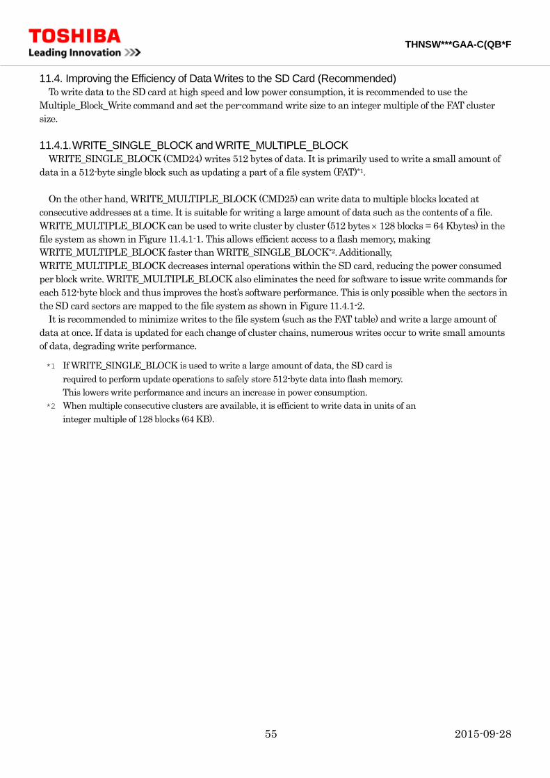
THNSW***GAA-C(QB*F
55 2015-09-28
11.4. Improving the Efficiency of Data Writes to the SD Card (Recommended)
To write data to the SD card at high speed and low power consumption, it is recommended to use the
Multiple_Block_Write command and set the per-command write size to an integer multiple of the FAT cluster
size.
11.4.1. WRITE_SINGLE_BLOCK and WRITE_MULTIPLE_BLOCK
WRITE_SINGLE_BLOCK (CMD24) writes 512 bytes of data. It is primarily used to write a small amount of
data in a 512-byte single block such as updating a part of a file system (FAT)*1.
On the other hand, WRITE_MULTIPLE_BLOCK (CMD25) can write data to multiple blocks located at
consecutive addresses at a time. It is suitable for writing a large amount of data such as the contents of a file.
WRITE_MULTIPLE_BLOCK can be used to write cluster by cluster (512 bytes 128 blocks = 64 Kbytes) in the
file system as shown in Figure 11.4.1-1. This allows efficient access to a flash memory, making
WRITE_MULTIPLE_BLOCK faster than WRITE_SINGLE_BLOCK*2. Additionally,
WRITE_MULTIPLE_BLOCK decreases internal operations within the SD card, reducing the power consumed
per block write. WRITE_MULTIPLE_BLOCK also eliminates the need for software to issue write commands for
each 512-byte block and thus improves the host’s software performance. This is only possible when the sectors in
the SD card sectors are mapped to the file system as shown in Figure 11.4.1-2.
It is recommended to minimize writes to the file system (such as the FAT table) and write a large amount of
data at once. If data is updated for each change of cluster chains, numerous writes occur to write small amounts
of data, degrading write performance.
*1 If WRITE_SINGLE_BLOCK is used to write a large amount of data, the SD card is
required to perform update operations to safely store 512-byte data into flash memory.
This lowers write performance and incurs an increase in power consumption.
*2 When multiple consecutive clusters are available, it is efficient to write data in units of an
integer multiple of 128 blocks (64 KB).
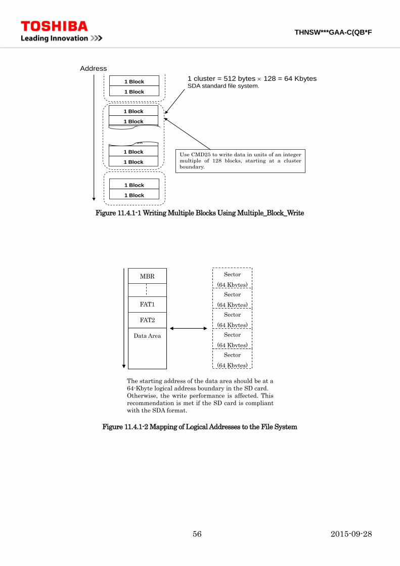
THNSW***GAA-C(QB*F
56 2015-09-28
1 cluster = 512 bytes 128 = 64 Kbytes SDA standard file system.
1 Block
1 Block
1 Block
1 Block
Address
1 Block
1 Block
1Block
1Block
1 Block
1 Block
Use CMD25 to write data in units of an integer
multiple of 128 blocks, starting at a cluster
boundary.
Figure 11.4.1-1 Writing Multiple Blocks Using Multiple_Block_Write
MBR
FAT1
FAT2
Data Area
The starting address of the data area should be at a
64-Kbyte logical address boundary in the SD card.
Otherwise, the write performance is affected. This
recommendation is met if the SD card is compliant
with the SDA format.
Sector
(64 Kbytes)
Sector
(64 Kbytes)
Sector
(64 Kbytes)
Sector
(64 Kbytes)
Sector
(64 Kbytes)
Figure 11.4.1-2 Mapping of Logical Addresses to the File System

THNSW***GAA-C(QB*F
57 2015-09-28
11.4.2. Write Flow Using WRITE_MULTIPLE_BLOCK
Figure 11.4.2-1 shows a flowchart for writing data using the WRITE_MULTIPLE_BLOCK command.
After issuing CMD25, the host should analyze its response and then send 512 bytes of data. The host should
continue to send data in units of 512 bytes, checking if the CRC Status is correct each time. Once the final block
has been written, the host should issue the Stop_Tran command (CMD12) to stop transmission.
Receive response
ERROR Check response
Send 512-byte write data
Receive CRC Status
Check CRC Status ERROR
Final block? NO
Issue CMD12
Check response ERROR
Issue CMD25
Postprocessing such as checking the number of blocks transferred using ACMD22
Error Processing Retry Operation
OK
YES
OK
OK
Figure 11.4.2-1 Write Flow Using WRITE_MULTIPLE_BLOCK

THNSW***GAA-C(QB*F
58 2015-09-28
11.4.3. Power Supply Control for the SD Card (Recommended)
It takes a maximum of one second*4 to initialize the SD card at power-on. Once the SD card is powered off, the
host needs to initialize it before it can perform the next read or write, lowering the card performance. To avoid
this situation, it is recommended to maintain the power supply to the SD card normally and remove it only when
the SD card is not accessed for a certain period. When the SD card is not accessed, it transitions to the Stand-by
State, reducing power consumption.
*4 Defined in the SD Physical Specification.
Cycling the Power Off and On to the SD Card
When the host powers off and on the SD card (i.e., when the host uses power cycling primarily to reduce power
consumption), it should power on the SD card after the voltage on the power supply line has dropped to the GND
level. If the interval between powering-off and powering-on is short, the SD card will not be reset properly. To
avoid this problem, it is recommended to keep the power supply below 0.5 V for at least 0.25 ms.
Figure 11.4.3-1 shows bad and good power cycling examples. Ensure that power cycling is performed properly
when creating a host design.
Power Supply Enable ON
OFF
3.3V
GND
VDD
In the bad power cycling example (a), VDD is disabled at #1 and enabled at #2 before VDD has dropped to the GND level. Consequently, the SD card might not be reset properly. (b) shows a recommended power cycling example. It is recommended to re-enable VDD after it has dropped to the GND level, as shown by #4. This way, the SD card is reset properly, improving reliability.
Power Supply Enable ON
OFF
3.3V
GND
VDD
#4
(a) Bad Power
Cycling
(b) Recommended Power Cycling
#2 #1
#3
Keep VDD at 0.5 V for at least 0.25 ms.
VDD does not drop to the GND level.
Figure 11.4.3-1 Power Supply Control

THNSW***GAA-C(QB*F
59 2015-09-28
11.5. Initialization in SPI Interface Mode (Required)
In SPI Interface mode, the host must initialize the SD card by using ACMD41, not CMD1.
11.6. Handling of the RSV Pins (Pins 8 and 9) in SPI Interface Mode (Required)
In SPI Interface mode, the RSV (reserved) pins (pins 8 and 9) must be pulled up with 10 k to 100 k.
11.7. The Don’ts During Write Operations (Required)
Don’t power off or pull the SD card out of a slot during write, read and mutual authentication operations;
otherwise, the card may be permanently damaged or data may be lost or corrupted.
The FlashAir SDHC memory card is designed to provide a certain level of protection for internal data even in
these situations, but it must be kept in mind that data might still become corrupted.
If there is any possibility that users will not follow this requirement, be sure to include a caution in the owner’s
manual of your end product.
11.8. SD Commands (Recommended)
1) Back-to-back issues of CMD0
When pin 1 (CD/DAT3) is driven Low, issuing CMD0 back-to-back causes the SD card to be initialized in SPI
mode. Great care should be taken as to the interval between issues of CMD0. This interval is affected by a
pull-up resistor on the host side; be sure to provide adequate considerations to a host design.
2) Security read commands
After ACMD18 or ACMD43 is issued, the host should ensure that the SD card has transitioned to the
Transmission State using CMD13 or allow for an interval of at least 100 µs before issuing the next command.
3) Issuing CMD12 (in SD mode) or Stop Tran Token (in SPI mode) after a block write command
To finish a multiple block write command (CMD25, ACMD25) early, CMD12 (STOP_TRANSMISSION) and
Stop Tran Token can be used in SD and SPI modes respectively. In this case, the host should issue CMD12 and
Stop Tran Token immediately after sending the last data block (within 400 µs after the Busy signal for the last
write data block is deasserted).
4) Intervals between SD commands
After the Busy signal on the SD bus for a command is deasserted, the host should allow for at least 15 µs before
issuing the next command. Otherwise, an SD bus error might occur or the device might not work properly.
11.9. Pull-up Resistors (Recommended)
The Command line (CMD) and the four Data lines (DAT[3:0]) should be pulled up with 10-k to 100-k
resistors on the host side, as defined in the specification. When these lines are pulled up on the host side, it is
recommended to disconnect the internal pull-up resistors in the card using ACMD42 after card detection.

THNSW***GAA-C(QB*F
60 2015-09-28
11.10. Other Guidelines (Recommended)
1) Erase sector size
The erase sector size can be calculated as follows using values contained in the CSD register:
erase sector size = block_length (SECTOR_SIZE) = 512 bytes 128 blocks = 64 Kbytes
(where block_length is the block length calculated from WRITE_BL_LEN.)
The host should erase an integer multiple of the erase sector size, starting at an erase sector boundary. It
should erase as much area as possible at a time.

THNSW***GAA-C(QB*F
61 2015-09-28
12. Firmware Specifications
For the firmware specifications, see the FlashAir Application Note.
13. Updating the Firmware
For how to update the firmware and the application software, contact Toshiba.

THNSW***GAA-C(QB*F
62 2015-09-28
14. List of Figures
Figure 3-1 SD Card (8GB Model) Design and Appearance .........................................................................................6
Figure 4-1 Major Use Cases of FlashAir .........................................................................................................................7
Figure 5.5-1 SD Device Interface Timing in the Default Mode ................................................................................ 10
Figure 5.5-2 SD Device Interface Timing in High-Speed Mode ............................................................................... 10
Figure 7-1 Write Protect Tab .......................................................................................................................................... 13
Figure 8.1-1 SDHC Card Pin Assignment ................................................................................................................... 14
Figure 8.2.1-1 SDHC memory Card Connections (in SD mode) .............................................................................. 15
Figure 8.2.2-1 SDHC memory Card Connections (in SPI Mode) ............................................................................. 17
Figure 8.3-1 Flowchart for SD Card Initialization ..................................................................................................... 20
Figure 8.4-1 SD Card Connections ............................................................................................................................... 21
Figure 11.1.1.3.1-1 Typical CMD25 Flow Including Error Recovery ...................................................................... 50
Figure 11.1.1.3.1-2 Retry Flow ....................................................................................................................................... 51
Figure 11.1.1.3.1-3 Recovery Write Flow ..................................................................................................................... 51
Figure 11.1.1.3.1-4 Exception Processing Flow for the Host .................................................................................... 51
Figure 11.1.1.3.2-1 Typical CMD18 Flow Including Error Recovery ...................................................................... 52
Figure 11.1.1.3.2-2 Read Retry Flow for CMD18 ....................................................................................................... 53
Figure 11.4.1-1 Writing Multiple Blocks Using Multiple_Block_Write .................................................................. 56
Figure 11.4.1-2 Mapping of Logical Addresses to the File System .......................................................................... 56
Figure 11.4.2-1 Write Flow Using WRITE_MULTIPLE_BLOCK .......................................................................... 57
Figure 11.4.3-1 Power Supply Control ......................................................................................................................... 58
15. List of Tables
Table 5.1-1 Design, Content and Logical Format ..........................................................................................................8
Table 5.2-1 Physical and Electrical Features .................................................................................................................8
Table 5.5-1 SD Device Interface Timing Parameters in the Default Speed Mode ................................................ 10
Table 5.5-2 SD Device Interface Timing Parameters in High-Speed Mode ........................................................... 10
Table 8.1-1 SDHC Card Pin Assignment ..................................................................................................................... 14
Table 8.2.1-1 List of Commands Supported in SD Mode .......................................................................................... 16
Table 8.2.2-1 List of Commands Supported in SPI Mode ......................................................................................... 18
Table 9.2-1 Internal Registers of the SD Card ............................................................................................................ 22
Table 9.2.1-1 OCR Register ............................................................................................................................................ 23
Table 9.2.2-1 CID Register.............................................................................................................................................. 24
Table 9.2.3-1 CSD Register ............................................................................................................................................. 26
Table 9.2.3-2 CSD_STRUCTURE ................................................................................................................................. 27
Table 9.2.3-3 TAAC Access Time Definition ................................................................................................................ 27
Table 9.2.3-4 Maximum Data Transfer Rate Definition ........................................................................................... 28
Table 9.2.3-5 Supported Card Command Class .......................................................................................................... 28
Table 9.2.3-6 Data Block Length ................................................................................................................................... 28
Table 9.2.3-7 WRITE_BLK_MISALIGN ..................................................................................................................... 29
Table 9.2.3-8 READ_BLK_MISALIGN ........................................................................................................................ 29
Table 9.2.3-9 DSR_IMP ................................................................................................................................................... 29
Table 9.2.3-10 ERASE_BLK_EN .................................................................................................................................. 30
Table 9.2.3-11 WP_GRP_ENABLE ............................................................................................................................... 30
Table 9.2.3-12 R2W_FACTOR ....................................................................................................................................... 30
Table 9.2.3-13 Data Block Length ................................................................................................................................. 31
Table 9.2.3-14 WRITE_BL_PARTIAL .......................................................................................................................... 31
Table 9.2.3-15 COPY ....................................................................................................................................................... 31
Table 9.2.3-16 PERM_WRITE_PROTECT ................................................................................................................. 32

THNSW***GAA-C(QB*F
63 2015-09-28
Table 9.2.3-17 TMP_WRITE_PROTECT .................................................................................................................... 32
Table 9.2.3-18 File Format ............................................................................................................................................. 32
Table 9.2.6-1 SCR Register ............................................................................................................................................. 33
Table 9.2.6-2 SCR_STRUCTURE ................................................................................................................................. 33
Table 9.2.6-3 SD_SPEC ................................................................................................................................................... 34
Table 9.2.6-4 Supported Security Algorithm ............................................................................................................... 34
Table 9.2.6-5 Supported Bus Widths ............................................................................................................................ 34
Table 9.2.6-6 SD_SPEC3 ................................................................................................................................................ 35
Table 9.2.7-1 SD Status ................................................................................................................................................... 35
Table 9.2.7-2 DAT_BUS_WIDTH .................................................................................................................................. 35
Table 9.2.7-3 SECURED_MODE .................................................................................................................................. 36
Table 9.2.7-4 SD_CARD_TYPE ..................................................................................................................................... 36
Table 9.2.7-5 SPEED_CLASS ........................................................................................................................................ 36
Table 9.2.7-6 PERFORMANCE_MOVE ...................................................................................................................... 37
Table 9.2.7-7 AU_SIZE .................................................................................................................................................... 37
Table 9.2.7-8 Maximum AU_SIZE ................................................................................................................................ 37
Table 9.2.7-9 ERASE_SIZE ............................................................................................................................................ 38
Table 9.2.7-10 ERASE_TIMEOUT ............................................................................................................................... 38
Table 9.2.7-11 ERASE_OFFSET ................................................................................................................................... 38
Table 9.2.8-1 CCCR Revision ......................................................................................................................................... 39
Table 9.2.8-2 SDIO Revision .......................................................................................................................................... 39
Table 9.2.9-1 Standard SDIO Function Interface Code............................................................................................. 40
Table 9.2.9-2 Standard iSDIO Function Interface Code ........................................................................................... 40
Table 9.2.9-3 iSDIO Type Support Code ...................................................................................................................... 41
Table 9.3.1-1 Sizes of SD Card Areas ............................................................................................................................ 43
Table 9.3.2-1 SD Card System Information ................................................................................................................ 43
Table 9.3.3-1 Master Boot Record and Partition Table .............................................................................................. 44
Table 9.3.3-2 Partition Table .......................................................................................................................................... 44
Table 9.3.3-3 Extended FDC Descriptor ...................................................................................................................... 45
Table 9.3.4-1 FAT ............................................................................................................................................................. 46
Table 11.3-1 Recommended Timeout Periods for Various Cases ............................................................................. 54
Table 11.3-2 Erase Times for SD Cards with Various Capacities ............................................................................ 54

THNSW***GAA-C(QB*F
64 2015-09-28
Annex. 1. Card Appearance
Annex 1-1. 8GB Model Toshiba Standard Design
Front
Back
THNSW008GAA-C (QB8F
Toshiba standard label position
Write Protect
Radio Certification Mode
l Name Toshiba Model Name
Japan Marking and
Certification No.
CE Marking
(Radio Equipment and
Telecommunications
Terminal Equipment)
Waste Disposal Law
USA Radio Certification No.
Canadian Radio Certification No.
Lot Management No
Wireless LAN MAC Address
Country of Manufacture Manufacturer
China Radio
Certification No.

THNSW***GAA-C(QB*F
65 2015-09-28
Annex 1-2. 16GB Model Toshiba Standard Design
Front
Back
THNSW016GAA-C (QB8F
Toshiba standard label position
Write Protect
Radio Certification Mode
l Name Toshiba Model Name
Japan Marking and
Certification No.
CE Marking
(Radio Equipment and
Telecommunications
Terminal Equipment)
Waste Disposal Law
USA Radio Certification No.
Canadian Radio Certification No.
Lot Management No
Wireless LAN MAC Address
Country of Manufacture Manufacturer
China Radio
Certification No.

THNSW***GAA-C(QB*F
66 2015-09-28
Annex 1-3. 32GB Model Toshiba Standard Design
Front
Back
THNSW032GAA-C (QB8F
Toshiba standard label position
Write Protect
Radio Certification Mode
l Name Toshiba Model Name
Japan Marking and
Certification No.
CE Marking
(Radio Equipment and
Telecommunications
Terminal Equipment)
Waste Disposal Law
USA Radio Certification No.
Canadian Radio Certification No.
Lot Management No
Wireless LAN MAC Address
Country of Manufacture Manufacturer
China Radio
Certification No.

THNSW***GAA-C(QB*F
67 2015-09-28
Annex 1-4. 8GB Model OEM Standard Design
Front
Back
THNSW008GAA-C (QB6F
Label position
Write Protect
Radio Certification Mode
l Name Toshiba Model Name
Japan Marking and
Certification No.
CE Marking
(Radio Equipment and
Telecommunications
Terminal Equipment)
SDHC Logo
USA Radio Certification No.
Canadian Radio Certification No.
Lot Management No
Wireless LAN MAC Address
Country of Manufacture Speed Class
Toshiba Logo

THNSW***GAA-C(QB*F
68 2015-09-28
Annex 1-5. 16GB Model OEM Standard Design
Front
Back
THNSW016GAA-C (QB6F
Label position
Write Protect
Radio Certification Mode
l Name Toshiba Model Name
Japan Marking and
Certification No.
CE Marking
(Radio Equipment and
Telecommunications
Terminal Equipment)
SDHC Logo
USA Radio Certification No.
Canadian Radio Certification No.
Lot Management No
Wireless LAN MAC Address
Country of Manufacture Speed Class
Toshiba Logo

THNSW***GAA-C(QB*F
69 2015-09-28
Annex 1-6. 32GB Model OEM Standard Design
Front
Back
THNSW032GAA-C (QB6F
Label position
Write Protect
Radio Certification Mode
l Name Toshiba Model Name
Japan Marking and
Certification No.
CE Marking
(Radio Equipment and
Telecommunications
Terminal Equipment)
SDHC Logo
USA Radio Certification No.
Canadian Radio Certification No.
Lot Management No
Wireless LAN MAC Address
Country of Manufacture Speed Class
Toshiba Logo

THNSW***GAA-C(QB*F
70 2015-09-28
Annex 1-7. SD Card Outline Dimensions
0.7 0.6
0.7
0.2
凹0.095
Unit:mm
Tolerance: 0.15 unless otherwise specified

THNSW***GAA-C(QB*F
71
Annex 1-8. Backside Laser Marking
1) 8GB Toshiba-brand model
<Description>
Line 1: Toshiba Corporation
Manufacturer
Line 2: MADE IN JAPAN
Country of origin
Line 3: Wireless LAN MAC Address
Line 4: Weekly code & key number
The first two digits denote the last two digits of the year, and the next two digits denote the week of the
year. The last six digits are the lot number managed by Toshiba.
Line 5: CMIIT ID: 2014DJ4823
China radio certification number
Line 6: Industry Canada ID: 9906A-P42350FA3
Canadian radio certification number
Line 7: FCC ID: ZVZP42350FA3
USA radio certification number
Line 8: CE0560
EU CE Marking and Notified Body number for radio conformity assessment
Line 9: Japanese certification marking and number
Japanese radio and terminal equipment certification number
line height: 1.0mm
line gap:0.6mm
Unit: mm

THNSW***GAA-C(QB*F
72
Line 10: Model number
Spec (Capacity) Toshiba Model Number Country of Origin Laser Marking
8-GB SDHC memory card with embedded
wireless LAN
THNSW008GAA-C MADE IN JAPAN THNSW008GAA-C
Line 11: WLSDTHNSWAAC
Radio certification model number
Waste Disposal Law mark

THNSW***GAA-C(QB*F
73
2) 16GB Toshiba-brand model
<Description>
Line 1: Toshiba Corporation
Manufacturer
Line 2: MADE IN JAPAN
Country of origin
Line 3: Wireless LAN MAC Address
Line 4: Weekly code & key number
The first two digits denote the last two digits of the year, and the next two digits denote the week of the
year. The last six digits are the lot number managed by Toshiba.
Line 5: CMIIT ID:CMIIT ID: 2014DJ4821
China radio certification number
Line 6: Industry Canada ID:9906A-P42350FA3
Canadian radio certification number
Line 7: FCC ID: ZVZP42350FA3
USA radio certification number
Line 8: CE0560
EU CE Marking and Notified Body number for radio conformity assessment
Line 9: Japanese certification marking and number
Japanese radio and terminal equipment certification number
line height: 1.0mm
line gap:0.6mm
Unit: mm

THNSW***GAA-C(QB*F
74
Line 10: Model number
Spec (Capacity) Toshiba Model Number Country of Origin Laser Marking
16-GB SDHC memory card with embedded
wireless LAN
THNSW016GAA-C MADE IN JAPAN THNSW016GAA-C
Line 11:WLSDTHNSWAAC
Radio certification model number
Waste Disposal Law mark:

THNSW***GAA-C(QB*F
75
3) 32GB Toshiba-brand model
<Description>
Line 1: Toshiba Corporation
Manufacturer
Line 2: MADE IN JAPAN
Country of origin
Line 3: Wireless LAN MAC Address
Line 4: Weekly code & key number
The first two digits denote the last two digits of the year, and the next two digits denote the week of the
year. The last six digits are the lot number managed by Toshiba.
Line 5: CMIIT ID:CMIIT ID: 2014DJ4822
mainland China radio certification number
Line 6: Industry Canada ID:9906A-P42350FA3
Canadian radio certification number
Line 7: FCC ID: ZVZP42350FA3
USA radio certification number
Line 8: CE0560
EU CE Marking and Notified Body number for radio conformity assessment
Line 9: Japanese certification marking and number
Japanese radio and terminal equipment certification number
line height: 1.0mm
line gap:0.6mm
Unit:mm

THNSW***GAA-C(QB*F
76
Line 10: Model number
Spec (Capacity) Toshiba Model Number Country of Origin Laser Marking
32-GB SDHC memory card with embedded
wireless LAN
THNSW032GAA-C MADE IN JAPAN THNSW032GAA-C
Line 11:WLSDTHNSWAAC
Radio certification model number
Waste Disposal Law mark:

THNSW***GAA-C(QB*F
77
4) 8GB OEM models
<Description>
Line 1: TOSHIBA
TOSHIBA Logo
Line 2: MADE IN JAPAN
Country of origin
Line 3: Wireless LAN MAC Address
Line 4: Weekly code & key number
The first two digits denote the last two digits of the year, and the next two digits denote the week of the
year. The last six digits are the lot number managed by Toshiba.
Line 5: Industry Canada ID: 9906A-P42350FA3
Canadian radio certification number
Line 6: FCC ID: ZVZP42350FA3
USA radio certification number
Line 7: CE0560
EU CE Marking and Notified Body number for radio conformity assessment
Line 8: Japanese certification marking and number
Japanese radio and terminal equipment certification number
line height: 1.0mm
line gap:0.9mm
Unit:mm

THNSW***GAA-C(QB*F
78
Line 9: Model number
Spec (Capacity) Toshiba Model Number Country of Origin Laser Marking
8-GB SDHC memory card with embedded
wireless LAN
THNSW008GAA-C MADE IN JAPAN THNSW008GAA-C
Line 10: WLSDTHNSWAAC
Radio certification model number
SDHC mark:
SD speed class:

THNSW***GAA-C(QB*F
79
5) 16GB OEM models
<Description>
Line 1: TOSHIBA
TOSHIBA Logo
Line 2:MADE IN JAPAN
Country of origin
Line 3: Wireless LAN MAC Address
Line 4: Weekly code & key number
The first two digits denote the last two digits of the year, and the next two digits denote the week of the
year. The last six digits are the lot number managed by Toshiba.
Line 5:Industry Canada ID: 9906A-P42350FA3
Canadian radio certification number
Line 6:FCC ID: ZVZP42350FA3
USA radio certification number
Line 7:CE0560
EU CE Marking and Notified Body number for radio conformity assessment
Line 8: Japanese certification marking and number
Japanese radio and terminal equipment certification number
line height: 1.0mm
line gap:0.9mm
Unit:mm

THNSW***GAA-C(QB*F
80
Line 9: Model number
Spec (Capacity) Toshiba Model Number Country of Origin Laser Marking
16-GB SDHC memory card with embedded
wireless LAN
THNSW016GAA-C MADE IN JAPAN THNSW016GAA-C
Line 10:WLSDTHNSWAAC
Radio certification model number
SDHC mark:
SD speed class:

THNSW***GAA-C(QB*F
81
6) 32GB OEM models
<Description>
Line 1: TOSHIBA
TOSHIBA Logo
Line 2:MADE IN JAPAN
Country of origin
Line 3: Wireless LAN MAC Address
Line 4: Weekly code & key number
The first two digits denote the last two digits of the year, and the next two digits denote the week of the
year. The last six digits are the lot number managed by Toshiba.
Line 5:Industry Canada ID: 9906A-P42350FA3
Canadian radio certification number
Line 6:FCC ID: ZVZP42350FA3
USA radio certification number
Line 7:CE0560
EU CE Marking and Notified Body number for radio conformity assessment
Line 8: Japanese certification marking and number
Japanese radio and terminal equipment certification number
line height: 1.0mm
line gap:0.9mm
Unit:mm

THNSW***GAA-C(QB*F
82
Line 9: Model number
Spec (Capacity) Toshiba Model Number Country of Origin Laser Marking
32-GB SDHC memory card with embedded
wireless LAN
THNSW032GAA-C MADE IN JAPAN THNSW032GAA-C
Line 10:WLSDTHNSWAAC
Radio certification model number
SDHC mark:
SD speed class:

THNSW***GAA-C(QB*F
83
Annex. 2. Packing
Inner Packing
FlashAir
1. Tray (4 10 = 40 pcs)
2. Plastic Bag
10 full trays and one empty tray = 11 trays
3. Inner Box (Note 1)
5. Barcode Label (T-1)
6. QA Seal
4. Adhesive Tape
79mm
(External Size)
195mm (External Size)
355mm (External Size)
External Packing
Note 1: If necessary, add
packing material (8PA48HA) on
top of a tray stack for a snug fit in
the inner carton.
Note 2: Add empty cartons
or gap fillers around inner
cartons for a snug fit in the outer
box.
7. Outer Box (Note 2)
8. Adhesive Tape
9. Barcode Label (T-1)
2 x 3 = 6 Inner Boxes
255mm (External Size)
370mm (External Size)
410mm (External Size)

THNSW***GAA-C(QB*F
84
P/N: TOSHIBA
TYPE THNSW008GAA-C
ADDC (QB8F Q'TY 400 pcs
**$$$$ YYWWKAZ - 400 480
RoHS_COMPATIBLE,_[[Pb]]>MCV DIFFUSED IN JAPAN
(Y) 205G3001 000400 XKA**$$$ ASSEMBLED IN JAPAN
YYWW
BC D E I
F
G
H
J
K
L
M
N
A
Annex. 3. Barcode Label
Annex 3-1. Print examples: 8GB Toshiba-brand model
Print example
Items Print examples Notes
A P/N No printing Spec
B TYPE THNSW008GAA-C Model name (without ADD.C)
C ADD.C (QB8F Additional Code
D QTY 400pcs Quantity
E Manufacturing Code 480 MP: “480”
F Key # **$$$$ Lot KeyNo.
G Weekly+Qty YYWWKBZ - 400 Weekly code + Control code (MP:KBZ,) + Quantity
H ECO info RoHS_COMPATIBLE._[[Pb]]>MCV Fixed “RoHS conformity” products (An adaptation
exclusion use is included.)
I TOSHIBA Logo TOSHIBA Fixed
J Country of origin
(Diffused)
DIFFUSED IN JAPAN Fixed
K Country of origin
(Assembly)
ASSEMBLED IN JAPAN Fixed
L Weekly YYWW As same as Weekly of “G”
M Barcode 2D - Barcode 2D - 2D Spec Reference
N Barcode 1D (Y) 205G3001 000400 XKA**$$$ Barcode 1D - 1D Spec Reference

THNSW***GAA-C(QB*F
85
Annex 3-2. 1D Spec.
P/N: TOSHIBA
TYPE THNSW008GAA-C
ADDC (QB8F Q'TY 400 pcs
**$$$$ YYWWKAZ - 400 480
RoHS_COMPATIBLE,_[[Pb]]>MCV DIFFUSED IN JAPAN
(Y) 205G3001 000400 XKA**$$$ ASSEMBLED IN JAPAN
YYWW
(1)
(2) (3) (5) (6)(4)
No. digit Digit number
print examples Discription (Input & Label display)
(1) 1 1 Y Fixed “Y” (TOSHIBA) original code, The display on a label “(Y)”
(2) 2-9 8 205G3001 Product code (Refer to individual purchase specifications of each memory card product)
(3) 10-15 6 000400 Quantity
(4) 16-17 2 XK Warehouse classification (480:XK)
(5) 18 1 A (1) When Weekly is lot , define a code after dividing a single figure younger into the first half and the second half.
A single digit younger 1 2 3 4 5 6 7 8 9 0
F B F B F B F B F B F B F B F B F B F B
A B C D E F G H I J K L M N O P Q R S T
the standard of the first half and the second half is the first half from the 1st week to the 26th week ,and the second half to the 27th week or subsequent ones
(2) when it is a lot without weekly, apply a single figure younger's number (0-9)
(6) 19-20 21-22 23
2 2 1
** $$ $
The double digit head of Key No.
The code which changed the 3-5th digits of Key No. into 36 base. The 6th figure of Key No.
Total 23 code
(Fixed) Product code Quantity
single figure younger
*Quantity considers it as a 6-figure display by right-justification, and a blank displays "0." (print examples: 400 -> 000400)
Warehouse classification
Key #(Finishing [conversion])

THNSW***GAA-C(QB*F
86
Annex 3-3. 2D Spec.
P/N: TOSHIBA
TYPE THNSW008GAA-C
ADDC (QB8F Q'TY 400 pcs
**$$$$ YYWWKAZ - 400 480
RoHS_COMPATIBLE,_[[Pb]]>MCV DIFFUSED IN JAPAN
(Y) 205G3001 000400 XKA**$$$ ASSEMBLED IN JAPAN
YYWW
(c)
(d)
(g)
(h)
(n)
(a)
(b)
(i)
(k) (l) (m)
(o)
(p)
(q)
(r)
(f)(e)
No. digit Digit number
print examples Discription (Input & Label display)
(a) 1 1 Y Fixed “Y” (TOSHIBA) original code
(b) 2-9 8 205G3001 Product code (Refer to individual purchase specifications of each memory card product)
(c) 10-34 25 THNSW008GAA-C Product name(ADD.C un-displaying.) (Refer to individual purchase specifications of each memory card product)
(d) 35-58 24 (QB8F Additional (Refer to individual purchase specifications of each memory card product)
(e) 59-83 25 (Blank) Fixed “Space” With no label display(CustomerP/N)
(f) 84-91 8 00000400 Quantity
(g) 92-94 3 GP1 Eco Code... Label display “RoHS COMPATIBLE [[Pb]]>MCV”
(h) 95-97 3 480 MP: "480"
(i) 98 1 (Blank) Fixed “Space”... Label display “TOSHIBA” Logo
(j) 99-103 5 (Blank) Fixed “Space”
(k) 104-105 2 XK Warehouse classification (480:XK)
(l) 106 1 A (1) When Weekly is lot , define a code after dividing a single figure younger into the first half and the second half.
A single digit younger 1 2 3 4 5 6 7 8 9 0
F B F B F B F B F B F B F B F B F B F B
A B C D E F G H I J K L M N O P Q R S T
* the standard of the first half and the second half is the first half from the 1st week to the 26th week ,and the second half to the 27th week or subsequent ones
(2) when it is a lot without weekly, apply a single figure younger's number (0-9)
(m) 107-‘108 2 ** The double digit head of Key No.
109-‘110 2 $$ The code which changed the 3-5th digits of Key No. into 36 base.
# 1 $ The 6th figure of Key No.
(n) 112-126 15 **$$$$ Key No.
(o) 127-133 7 YYWWK B Z Weekly Code(3 figures of ends are semi-contest person management codes.)
(p) 134-137 4 YYWW Weekly ... Manufacture week
(q) 138-139 2 JP Fixed “JP” ... Label display “DIFFUSED IN JAPAN”
(r) 140-141 2 JP Fixed “JP” ... Label display “ASSEMBLED IN JAPAN”
(s) 142-143 2 (Blank) Fixed “00” ... With no label display
(t) 144 1 0 Fixed “Space”
(u) 145-146 2 (Blank) Fixed “00” ... With no label display
(v) 147-151 5 (Blank) Fixed “Space”
(w) 152-153 2 (Blank) Fixed “Space”
(x) 154-186 33 (Blank) Fixed “Space”
(y) 187-189 3 (Blank) Fixed “Space”
(z) 190-195 6 (Blank) Fixed “Space”
(aa) 196-197 2 (Blank) Fixed “Space”
(ab) 198-200 3 (Blank) Fixed “Space”
(j)(e)(s)(t)(u)(v)(w)(y)(z)(aa)(ab)
No display onthe Carton label

THNSW***GAA-C(QB*F
87
An outside dimension / printing size
dig i t 1 2 3 4 5 6 7 8 9 10 11 12 13 14 15 16 17 18 19 20 21 22 23 24 25 26 27 28 29 30 31 32 33 34
Y 2 0 5 G 3 0 0 1 T H N S W 0 0 8 G A A - C
(a) (b) (c)Product Code Product Type Name
(Fixed)dig i t 35 36 37 38 39 40 41 42 43 44 45 46 47 48 49 50 51 52 53 54 55 56 57 58
( Q B 8 F
(d)Additional Code
dig i t 59 60 61 62 63 64 65 66 67 68 69 70 71 72 73 74 75 76 77 78 79 80 81 82 83 84 85 86 87 88 89 90 91
0 0 0 0 0 4 0 0
(e) (f)(Blank) Quantity
dig i t 92 93 94 95 96 97 98 99 100 101 102 103 104 105 106 107 108 109 110 111 112 113 114 115 116 117 118 119 120 121 122 123 124 125 126
G P 1 4 8 0 X K A * * $ $ $ * * $ $ $ $
(g) (h) (i) (j) (l) (m) (n)Eco Code Warehouse (Blank) Coverted Key # Key #
Code (Blank) division Yeardig i t 127 128 129 130 131 132 133 134 135 136 137 138 139 140 141 142 143 144 145 146 147 148 149 150 151 152 153
Y Y W W K A Z Y Y W W J P J P 0 0 0
(o) (t) (v)Weekly Code Label Issued (Blank)
Weekly (Blank)dig i t 154 155 156 157 158 159 160 161 162 163 164 165 166 167 168 169 170 171 172 173 174 175 176 177 178 179 180 181 182 183 184 185 186
(x)Local Product Name
dig i t 187 188 189 190 191 192 193 194 195 196 197 198 199 200
(y) (ab)(Blank) (Blank)
※Data are left-aligned basically. "Spece" is set in the blank. However, only quantity should be right-aligned. Set "0" in the blank. (Example: 400 → 00000400)
(k)Warehouse
(p) (q) (r) (s)(Fixed) (Fixed) (Fixed)
(u)(Fixed) (Blank)
(w)
(aa)(Blank) (Blank)
(z)

THNSW***GAA-C(QB*F
88

THNSW***GAA-C(QB*F
89
Annex. 4. Clauses To Be Included in an Instruction Manual
It is advisable to include these or similar sentences in an instruction manual regarding to the
handling of an SD card.
About SD memory cards
The SD memory card is a storage medium compliant with the Secure Digital Music Initiative
(SDMI) standard to provide for the protection of the rights of copyright holders. With embedded
semiconductor memory, an SD card allows you to store and modify data in it.
Limitation of Liability
a) xxx Corporation (your company name) assumes no liability for damage or losses due to fire,
earthquake, acts of third parties, other accidents, negligent or intentional misuse or use in
any other abnormal condition.
b) xxx Corporation (your company name) assumes no liability for damage or losses, lost
profits, or third party claims arising out of the use of, or inability to use, the Product.
c) xxx Corporation (your company name) assumes no liability for damage or losses occurring
as a result of noncompliance with the instructions in the enclosed product manual.
d) xxx Corporation (your company name) assumes no liability for destruction or loss of data
occurring during use of the Product, regardless of the cause, type, or scale of damage. (xxx
Corporation does not provide data recovery services.)
e) xxx Corporation (your company name) assumes no liability for damage or losses occurring
due to malfunctions resulting from a combination of connected devices and software.
Dos and Don’ts
a) Don’ts
・ Keep the Product out of reach of small children.
Accidental swallowing may cause suffocation or injury. Contact a doctor immediately
if you suspect a child has swallowed the Product.
・ Do not disassemble or modify the Product.
This may cause electric shock, damage to the Product, or fire.
・ Do not bend, crush, drop, or place heavy objects on top of the Product.
Do not use tweezers, pliers, or similar items that could damage the Product. Take
particular care when inserting or removing the Product. Stop using the Product when
the Product does not work properly. Failure to follow these instructions could result
in fire, damage to the Product and/or other property, and/or personal injury including
burns and electric shock.
b) Dos
・ If the Product produces noises, an odor, overheats or smokes, turn off the computer
and peripherals immediately and disconnect the power cord/cable from the power plug
socket, and do not touch the Product.
Failure to follow these instructions could result in fire, damage to the Product and/or
other property, and/or personal injury including burns and electric shock. Do not use
the Product again. Please contact your local XXX (your company name) sales
representative.

THNSW***GAA-C(QB*F
90
Handling Precautions
a) Do not directly touch the interface pins or put them in contact with metal. Failure to follow
this instruction may cause permanent destruction of the Product and/or loss of internal
data due to static electricity. Do not bend, drop or apply strong force to the Product. Failure
to follow these instructions could cause permanent destruction of the Product and/or loss of
internal data.
b) Do not disassemble or modify the Product.
c) Do not splash water on the Product or expose the Product to moisture. Do not place the
Product in a location exposed to corrosive chemicals or gasses. Failure to follow these
instructions could cause loss of internal data.
d) Do not turn off the power or remove the Card from a slot while writing data to or reading
data from the Card. Failure to follow this instruction may permanent destruction of the
Product and/or loss of internal data.
e) Reformatting the Product will cause all data stored in the Product to be lost. Before
reformatting, please back up all data you wish to save.
Notes on Usage
a) The Product comes pre-formatted in compliance with SD Memory Card standards. If
necessary, the Product must be reformatted using equipment with the SD logo mark that
provides a formatting capability for SD memory cards. Formatting with any other
equipment (such as a personal computer) may cause problems with the Product such as the
inability to read, write, or delete data.
b) The SD memory card is a storage medium compliant with the Secure Digital Music
Initiative (SDMI) standard to provide for the protection of the rights of copyright holders.
Part of the memory is reserved for use as a management data area defined by the SD
Memory Card standards. Thus, the available memory area is smaller than the capacity
shown on the Product label.
c) It is recommended to make a backup copy of the data stored in an SD memory card.
Slide the Write Protect tab to the end until it stops.

THNSW***GAA-C(QB*F
91
JAPAN
The manual for Japanese market have to indicate the below caution in Japanese.
DO NOT translate into another language, should be in Japanese.
電子機器の使用に関するご注意
このガイドは、この機器に適用される各国固有の無線通信に関する規定およびそれ以外の規定を掲載し
ています。
お使いの機器には、無線デバイスが内蔵されていますが、特定の環境において、無線デバイスの使用が
制限されることがあります。このような制限は、飛行機の機内、病院、爆発物の近く、危険な場所など
で適用される可能性があります。この製品の使用制限に関する方針が不明な場合は、製品を使用する前
に承諾を得てください。
この機器は、家庭環境で使用することを目的としていますが、この機器がラジオやテレビジョン受信機
に近接して使用されると、受信障害を引き起こすことがあります。
取扱説明書に従って正しい取扱をして下さい。
この機器はその他のアンテナや発信機のそばに設置したり同時に使用したりしないでください。
また、ペースメーカーや医療機器、航空機の計器類には、携帯電話や PHS 同様、障害を与える恐れが
ありますので、携帯電話や PHS 等と同様の使用ルールに従うようにしてください。
この機器の使用周波数帯では、電子レンジ等の産業・科学・医療用機器のほか工場の製造ライン等
で使用されている移動体識別用の構内無線局(免許を要する無線局)及び特定小電力無線局(免許を要
しない無線局)並びにアマチュア無線局(免許を要する無線局)が運用されています。
1. この機器を使用する前に、近くで移動体識別用の構内無線局及び特定小電力無線局並びにアマチュ
ア無線局が運用されていないことを確認して下さい。
2. 万一、この機器から移動体識別用の構内無線局に対して有害な電波干渉の事例が発生した場合には、
速やかに使用周波数を変更するか又は電波の発射を停止した上、下記連絡先にご連絡頂き、混信回
避のための処置等(例えば、パーティションの設置など)についてご相談して下さい。
3. その他、この機器から移動体識別用の特定小電力無線局あるいはアマチュア無線局に対して有害な
電波干渉の事例が発生した場合など何かお困りのことが起きたときは、次の連絡先へお問い合わせ
下さい。
連絡先:

THNSW***GAA-C(QB*F
92
Federal Communications Commission (FCC) Notice (USA)
This equipment has been tested and found to comply with the limits for a Class B digital device, pursuant to
Part 15 of the FCC Rules. These limits are designed to provide reasonable protection against harmful
interference in a residential installation. This equipment generates, uses, and can radiate radio frequency
energy and, if not installed and used in accordance with the instructions, may cause harmful interference to
radio communications. However, there is no guarantee that interference will not occur in a particular
installation. If this equipment does cause harmful interference to radio or television reception, which can be
determined by turning the equipment off and on, the user is encouraged to try to correct the interference by
one or more of the following measures:
● Reorient or relocate the receiving antenna.
● Increase the separation between the equipment and the receiver.
● Connect the equipment into an outlet on a circuit different from that to which the receiver is connected.
● Consult the dealer or an experienced radio or television technician for help.
Changes or modifications not expressly approved by the party responsible for compliance could void the
user’s authority to operate the equipment.
To comply with the FCC RF exposure compliance requirements, this device and its antenna must not be
co-located or operating in conjunction with any other antenna or transmitter.
Canadian Notice
This device complies with the Canadian ICES-003 Class B specifications and RSS-210 of Industry Canada.
This Class B digital apparatus meets all requirements of the Canadian Interference-Causing Equipment
Regulations. Wireless operation is subject to 2 conditions. The first is that the wireless device may not cause
interference. The second is that the wireless device must accept any interference, including interference that
may cause undesired operation of the device.
To comply with the Canadian RF exposure compliance requirements, this device and its antenna must not be
co-located or operating in conjunction with any other antenna or transmitter.
Avis Canadien
Cet appareil est conforme à la norme canadienne NMB-003 classe B et CNR-210 d'Industrie Canada.
Ce dispositif numérique de classe B respecte toutes les exigences du Règlement canadien matériel brouilleur.
Fonctionnement sans fil est soumis à deux conditions. La première est que l'appareil sans fil peut ne pas
provoquer des interférences. La seconde est que le dispositif sans fil doit accepter toute interférence, y
compris les interférences qui peuvent causer un mauvais fonctionnement de l'appareil.
Pour se conformer aux exigences de conformité RF canadienne l'exposition, cet appareil et son antenne ne
doivent pas être co-localisés ou fonctionnant en conjonction avec une autre antenne ou transmetteur.

THNSW***GAA-C(QB*F
93
European Union Regulatory Notice
This device bearing the CE marking is in compliance with the essential requirements and other relevant
provisions of Directive 1999/5/EC. This device complies with the following harmonized European standards.
Health: EN62479:2010
Safety: EN60950-1:2006, +A1:2010, +A11:2009, +A12:2011, +A2:2013
EMC : EN301 489-1 V1.9.2:2011, EN301 489-17 V2.2.1:2012
Radio: EN300 328 V1.8.1:2012
● The following CE marking is valid for EU non-harmonized telecommunications products.
Refer to the regulatory label provided on this product.
The telecommunications functionality of this product may be used in the following EU and EFTA countries:
Austria, Belgium, Bulgaria, Cyprus, Czech Republic, Croatia, Denmark, Estonia, Finland, France, Germany,
Greece, Hungary, Iceland, Ireland, Italy, Latvia, Liechtenstein, Lithuania, Luxembourg, Malta,
Netherlands, Norway, Poland, Portugal, Romania, Slovak Republic, Slovenia, Spain, Sweden,
Switzerland, and United Kingdom.
EU Declaration of Conformity: This Product carries the CE-Mark in accordance with the related European
Directives.
China
8GB Model
CMIIT ID : 2014DJ4823
16GB Model
CMIIT ID : 2014DJ4821
32GB Model
CMIIT ID : 2014DJ4822
Taiwan
CCAM14LP0220T3
第十二條 經型式認證合格之低功率射頻電機,非經許可,公司、商號或使用者均不得擅自變更頻率、加大
功率或變更原設計之特性及功能。
第十四條 低功率射頻電機之使用不得影響飛航安全及干擾合法通信;經發現有干擾現象時,應立即停用,
並改善至無干擾時方得繼續使用。
前項合法通信,指依電信法規定作業之無線電通信。
低功率射頻電機須忍受合法通信或工業、科學及醫療用電波輻射性電機設備之干擾。
* The minimum size of NCC Logo is 15mm in diameter.

THNSW***GAA-C(QB*F
94
Australia/New Zealand
RCM
South Korea (한국)
Please indicate KCC Mark in a package and a manual.
* The minimum size of KCC Logo is 5mm in height.
Please indicate the following cautions wording with KCC Logo mark in a manual.
Russia (Display needlessness)
(Planning)
Term of validity: (Planning)
* After going through the term of validity, the export to Russia and sale become impossible.
South Africa
Please stick on a manual or an individual packaging box.
* The minimum size of ICASA Logo is 3x3mm.
* For the other countries/regions, to be confirmed to Toshiba sales departments.
MSIP-CMM-TSD-THNSW032GAA-C

THNSW***GAA-C(QB*F
95
RESTRICTIONS ON PRODUCT USE
This document and any information herein may not be reproduced without prior written permission from TOSHIBA. Even with
TOSHIBA’s written permission, reproduction is permissible only if reproduction is without alteration/omission.
Though TOSHIBA works continually to improve Product's quality and reliability, Product can malfunction or fail. Customers are
responsible for complying with safety standards and for providing adequate designs and safeguards for their hardware, software and
systems which minimize risk and avoid situations in which a malfunction or failure of Product could cause loss of human life, bodily
injury or damage to property, including data loss or corruption. Before customers use the Product, create designs including the Product,
or incorporate the Product into their own applications, customers must also refer to and comply with (a) the latest versions of all
relevant TOSHIBA information, including without limitation, this document, the specifications, the data sheets and application notes for
Product and the precautions and conditions set forth in the "TOSHIBA Semiconductor Reliability Handbook" and (b) the instructions for
the application with which the Product will be used with or for. Customers are solely responsible for all aspects of their own product
design or applications, including but not limited to (a) determining the appropriateness of the use of this Product in such design or
applications; (b) evaluating and determining the applicability of any information contained in this document, or in charts, diagrams,
programs, algorithms, sample application circuits, or any other referenced documents; and (c) validating all operating parameters for
such designs and applications. TOSHIBA ASSUMES NO LIABILITY FOR CUSTOMERS' PRODUCT DESIGN OR APPLICATIONS.
Product is intended for use in general electronics applications (e.g., computers, personal equipment, office equipment, measuring
equipment, industrial robots and home electronics appliances) or for specific applications as expressly stated in this document.
Product is neither intended nor warranted for use in equipment or systems that require extraordinarily high levels of quality and/or
reliability and/or a malfunction or failure of which may cause loss of human life, bodily injury, serious property damage or serious public
impact (“Unintended Use”). Unintended Use includes, without limitation, equipment used in nuclear facilities, equipment used in the
aerospace industry, medical equipment, equipment used for automobiles, trains, ships and other transportation, traffic signaling
equipment, equipment used to control combustions or explosions, safety devices, elevators and escalators, devices related to electric
power, and equipment used in finance-related fields. Do not use Product for Unintended Use unless specifically permitted in this
document.
Do not disassemble, analyze, reverse-engineer, alter, modify, translate or copy Product, whether in whole or in part.
Product shall not be used for or incorporated into any products or systems whose manufacture, use, or sale is prohibited under any
applicable laws or regulations.
The information contained herein is presented only as guidance for Product use. No responsibility is assumed by TOSHIBA for any
infringement of patents or any other intellectual property rights of third parties that may result from the use of Product. No license to
any intellectual property right is granted by this document, whether express or implied, by estoppel or otherwise.
Absent a written signed agreement, except as provided in the relevant terms and conditions of sale for product, and to the maximum
extent allowable by law, TOSHIBA (1) assumes no liability whatsoever, including without limitation, indirect, consequential, special, or
incidental damages or loss, including without limitation, loss of profits, loss of opportunities, business interruption and loss of data, and
(2) disclaims any and all express or implied warranties and conditions related to sale, use of product, or information, including
warranties or conditions of merchantability, fitness for a particular purpose, accuracy of information, or noninfringement.
Do not use or otherwise make available Product or related software or technology for any military purposes, including without limitation,
for the design, development, use, stockpiling or manufacturing of nuclear, chemical, or biological weapons or missile technology
products (mass destruction weapons). Product and related software and technology may be controlled under the Japanese Foreign
Exchange and Foreign Trade Law and the U.S. Export Administration Regulations. Export and re-export of Product or related software
or technology are strictly prohibited except in compliance with all applicable export laws and regulations.
Product is subject to foreign exchange and foreign trade control laws.
The technical information described in this document is subject to foreign exchange and foreign trade control laws.
Please contact your TOSHIBA sales representative for details as to environmental matters such as the RoHS compatibility of Product.
Please use Product in compliance with all applicable laws and regulations that regulate the inclusion or use of controlled substances,
including without limitation, the EU RoHS Directive. TOSHIBA assumes no liability for damages or losses occurring as a result of
noncompliance with applicable laws and regulations.