first-principle natural band alignment of gan / …tansu/journals/journal_99.pdfaip advances 5,...
TRANSCRIPT

First-principle natural band alignment of GaN / dilute-As GaNAs alloyChee-Keong Tan and Nelson Tansu Citation: AIP Advances 5, 017129 (2015); doi: 10.1063/1.4906569 View online: http://dx.doi.org/10.1063/1.4906569 View Table of Contents: http://scitation.aip.org/content/aip/journal/adva/5/1?ver=pdfcov Published by the AIP Publishing
All article content, except where otherwise noted, is licensed under a Creative Commons Attribution 3.0 Unported license. See:
http://creativecommons.org/licenses/by/3.0/ Downloaded to IP: 207.172.231.174 On: Thu, 22 Jan 2015 14:23:22

AIP ADVANCES 5, 017129 (2015)
First-principle natural band alignment of GaN / dilute-AsGaNAs alloy
Chee-Keong Tana and Nelson Tansub
Center for Photonics and Nanoelectronics, Department of Electrical and ComputerEngineering, Lehigh University, Bethlehem, PA 18015, USA
(Received 13 December 2014; accepted 13 January 2015; published online 22 January 2015)
Density functional theory (DFT) calculations with the local density approximation(LDA) functional are employed to investigate the band alignment of dilute-As GaNAsalloys with respect to the GaN alloy. Conduction and valence band positions ofdilute-As GaNAs alloy with respect to the GaN alloy on an absolute energy scale aredetermined from the combination of bulk and surface DFT calculations. The resultingGaN / GaNAs conduction to valence band offset ratio is found as approximately5:95. Our theoretical finding is in good agreement with experimental observation,indicating the upward movements of valence band at low-As content dilute-AsGaNAs are mainly responsible for the drastic reduction of the GaN energy band gap.In addition, type-I band alignment of GaN / GaNAs is suggested as a reasonableapproach for future device implementation with dilute-As GaNAs quantum well,and possible type-II quantum well active region can be formed by using InGaN /dilute-As GaNAs heterostructure. C 2015 Author(s). All article content, except whereotherwise noted, is licensed under a Creative Commons Attribution 3.0 UnportedLicense. [http://dx.doi.org/10.1063/1.4906569]
I. INTRODUCTION
Owing to the desirable electronic and optoelectronic properties of nitride-based alloys, espe-cially the direct and large band gap in the Brillouin Zone, rapid development of InGaN, AlGaNand AlInN alloys have been witnessed in the past decade, leading to successful fabrication of LEDsoperating in the blue-green light emitting diodes (LEDs).1–10 While InGaN- and GaN-based alloyshave been widely implemented into solid state lighting applications, the InGaAs- and GaAs-basedalloys are established material systems for telecommunication and infrared device technologies.11,12 The mixed AsN-based alloys had been studied in the dilute-nitrogen regime specifically forresulting in some of the breakthroughs in the long wavelength lasers on GaAs.13–18 The findings ofdilute-nitride GaAs-based alloy had led into the state-of-the-art and low threshold laser devices forthe telecommunication applications.16–18 In contrast to the successful development on dilute-nitridealloys – based on InGaAsN, the research on dilute-arsenic (As) GaNAs-based alloy is at the earlystage. Dilute-arsenic GaNAs-based alloy has yet to be implemented into devices and the availableliterature published on this alloy subject is severely limited.5,19–28
Li and co-workers first succeeded in incorporating As into thin film GaN through metal-organicchemical vapor deposition (MOCVD), and the redshift of band gap energy of the dilute-As GaNAsalloy was observed in the photoluminescence study.5 Further studies have also shown successfulincorporation of As-content up to 7% into GaN material through MOCVD,20 and synthesis ofGaNAs alloy in full composition range through molecular beam epitaxy (MBE) was recently re-ported.21 Recent experimental work by Yu et al reported that the band gap of dilute-As GaNAs alloyreaches 2.3 eV ± 0.5 eV at roughly 6%-As impurities incorporation.21 Most recently, the electronicproperties of the dilute-As GaNAs alloy was studied and it was suggested that the alloy potentially
aElectronic mail: [email protected] mail: [email protected]
2158-3226/2015/5(1)/017129/8 5, 017129-1 ©Author(s) 2015
All article content, except where otherwise noted, is licensed under a Creative Commons Attribution 3.0 Unported license. See:
http://creativecommons.org/licenses/by/3.0/ Downloaded to IP: 207.172.231.174 On: Thu, 22 Jan 2015 14:23:22
017129-2 C.-K. Tan and N. Tansu AIP Advances 5, 017129 (2015)
has lower Auger recombination rate, which is essential to achieve suppression of Auger process athigh current density.22 These findings indicate that dilute-As GaNAs alloy as a promising materialfor visible light applications specifically for addressing the droop issue in LED technologies.
Nevertheless, in order to implement dilute-As GaNAs alloy in devices such as LEDs, semi-conductor heterostructures between dilute-As GaNAs alloy and GaN alloy need to be formed. Theunderstanding of the band discontinuities for two different III-V or III-Nitride materials is crit-ical10,15,29–38 for designing nanostructures or heterostructures applicable in device implementation.Up to today, there has been no comprehensive and conclusive study in predicting and determiningthe natural band alignment between GaN and dilute-As GaNAs alloy. Therefore the understandingof the band discontinuity of GaNAs / GaN will be essential for evaluating the optical and carriertransport properties in devices incorporating this heterostructure.
In this work, we present a comprehensive quantitative analysis of the relative natural bandalignment of dilute-As GaNAs / GaN heterostructures using First-Principle method. We examinethe natural band offsets of the strain-free dilute-As GaNAs alloy relative to the GaN alloy. Inaddition to that, we also discussed about the source of the drastic reduction of the band gap fromanalyzing the band offset between GaN and dilute-As GaNAs alloy, in which the upward movementof the valence band of the dilute-As GaNAs alloy was shown to contribute significantly to thiseffect. Our finding provides useful understanding of the band parameters important for enablingthe implementation of dilute-As GaNAs alloy and heterostructures in GaN-based electronics andoptoelectronics device technologies.
II. COMPUTATIONAL METHOD
The determination of band offsets between two materials can be performed through the pro-jected local density of states calculation (LDOS)29 and also the potential line-up method.30,31 Whileboth methods are capable of providing insight on how the alignment between two materials shouldbe, the potential line-up method is chosen in this work simply because the LDOS calculation re-quires higher demand of convergence parameters which were previously identified, resulting in aslower convergence compared to that of the charge density.32 Note that the natural band alignmentof the unstrained system (GaN / dilute-As GaNAs) is focused in our DFT calculation. The advan-tage of this alignment for a material system is that it can be directly connected to the physicalsituation of photoelectrode33,34 and active regions for lasers or LEDs.27,28 In the potential line-upmethod, the calculation of valence band offset (VBO) between two different materials is a combina-tion of two terms which are the band structure term (∆Ev) and the electrostatic term (∆V). For theband structure term, it is defined as the difference between the top of the valence bands of two bulkmaterials with respect to the average electrostatic potential at core. The information of the valencebands of the bulk materials can be obtained from two independent standard bulk band structurecalculations. For the electrostatic potential term, it is obtained from the lineup of the macroscopicaverage electrostatic potential in two material slabs, by aligning it with respect to the vacuum levelin the slabs.33
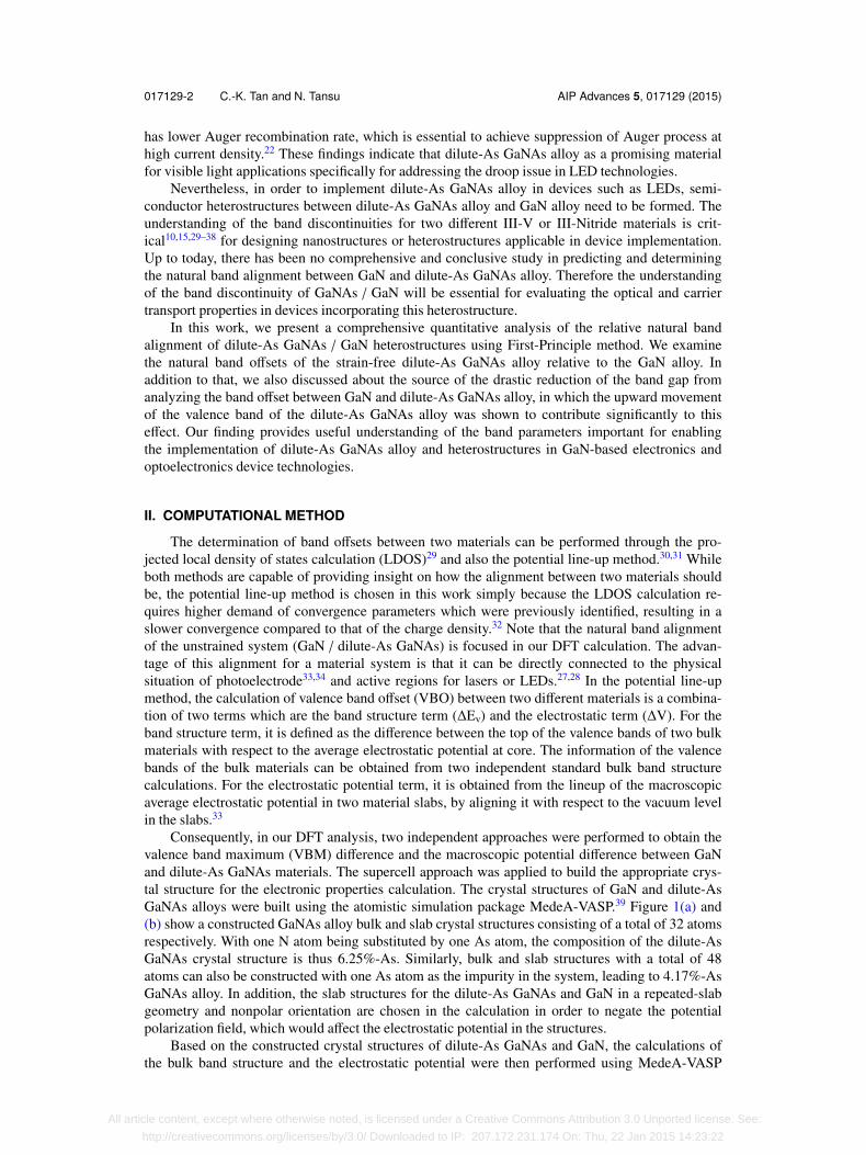
Consequently, in our DFT analysis, two independent approaches were performed to obtain thevalence band maximum (VBM) difference and the macroscopic potential difference between GaNand dilute-As GaNAs materials. The supercell approach was applied to build the appropriate crys-tal structure for the electronic properties calculation. The crystal structures of GaN and dilute-AsGaNAs alloys were built using the atomistic simulation package MedeA-VASP.39 Figure 1(a) and(b) show a constructed GaNAs alloy bulk and slab crystal structures consisting of a total of 32 atomsrespectively. With one N atom being substituted by one As atom, the composition of the dilute-AsGaNAs crystal structure is thus 6.25%-As. Similarly, bulk and slab structures with a total of 48atoms can also be constructed with one As atom as the impurity in the system, leading to 4.17%-AsGaNAs alloy. In addition, the slab structures for the dilute-As GaNAs and GaN in a repeated-slabgeometry and nonpolar orientation are chosen in the calculation in order to negate the potentialpolarization field, which would affect the electrostatic potential in the structures.
Based on the constructed crystal structures of dilute-As GaNAs and GaN, the calculations ofthe bulk band structure and the electrostatic potential were then performed using MedeA-VASP
All article content, except where otherwise noted, is licensed under a Creative Commons Attribution 3.0 Unported license. See:
http://creativecommons.org/licenses/by/3.0/ Downloaded to IP: 207.172.231.174 On: Thu, 22 Jan 2015 14:23:22
017129-3 C.-K. Tan and N. Tansu AIP Advances 5, 017129 (2015)
FIG. 1. (a) Supercell and (b) Slab of GaNAs alloy built using MedeA-VASP package. These 32-atom supercell consists of16 Gallium (Ga) atoms, 15 Nitrogen (N) atoms and 1 Arsenic (As) atom, corresponding to 6.25% As-content in GaNAs alloy.
with projected augmented wave pseudopotentials (PAW) method implemented in the code.39 Localdensity approximation (LDA) exchange-correlation potential was used in the DFT calculation.39,40
The electronic wave functions are described in plane wave basis with the cutoff energy fixedat 400 eV. The structure optimization was performed by relaxing the atom positions with theHellmann-Feynman force set to 0.02 eV/Å before the calculation takes place. The energy conver-gence tolerance was set at 1 x 10⁻⁵ eV/atom, while the external stress was set to 0 GPa. TheGamma-centered Monkhorst-Pack grid and high symmetry k-points were used for the band struc-ture and the electrostatic potential calculations. Note that different Monkhorst-Pack k-point mesheswere generated in the calculations attributed to the use of different supercell and slab sizes.The spin-orbit coupling was excluded in both calculations since the effect in the wide band gapIII-nitride semiconductor is negligible. These parameters were consistently used in both supercelland slab approaches.
III. RESULTS AND DISCUSSIONS
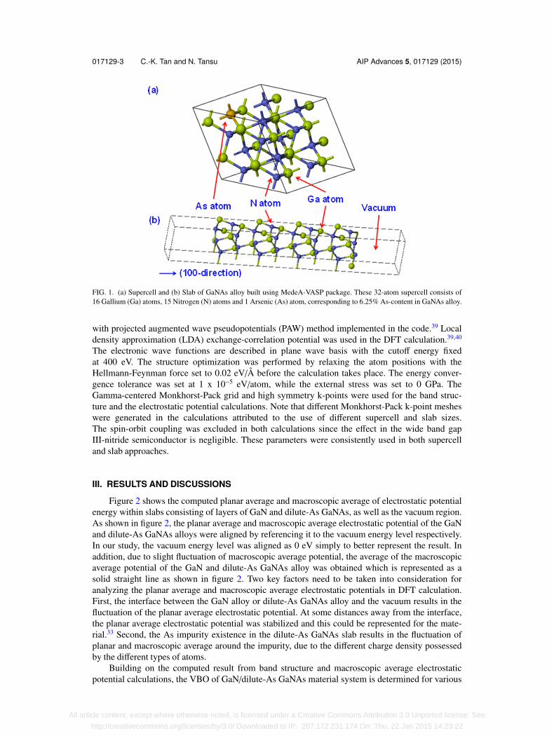
Figure 2 shows the computed planar average and macroscopic average of electrostatic potentialenergy within slabs consisting of layers of GaN and dilute-As GaNAs, as well as the vacuum region.As shown in figure 2, the planar average and macroscopic average electrostatic potential of the GaNand dilute-As GaNAs alloys were aligned by referencing it to the vacuum energy level respectively.In our study, the vacuum energy level was aligned as 0 eV simply to better represent the result. Inaddition, due to slight fluctuation of macroscopic average potential, the average of the macroscopicaverage potential of the GaN and dilute-As GaNAs alloy was obtained which is represented as asolid straight line as shown in figure 2. Two key factors need to be taken into consideration foranalyzing the planar average and macroscopic average electrostatic potentials in DFT calculation.First, the interface between the GaN alloy or dilute-As GaNAs alloy and the vacuum results in thefluctuation of the planar average electrostatic potential. At some distances away from the interface,the planar average electrostatic potential was stabilized and this could be represented for the mate-rial.33 Second, the As impurity existence in the dilute-As GaNAs slab results in the fluctuation ofplanar and macroscopic average around the impurity, due to the different charge density possessedby the different types of atoms.
Building on the computed result from band structure and macroscopic average electrostaticpotential calculations, the VBO of GaN/dilute-As GaNAs material system is determined for various
All article content, except where otherwise noted, is licensed under a Creative Commons Attribution 3.0 Unported license. See:
http://creativecommons.org/licenses/by/3.0/ Downloaded to IP: 207.172.231.174 On: Thu, 22 Jan 2015 14:23:22

017129-4 C.-K. Tan and N. Tansu AIP Advances 5, 017129 (2015)
FIG. 2. The planar average (solid line) and the macroscopic average (dot line) of the electrostatic potential near the surfacefor GaN and dilute-As GaNAs alloys computed within the DFT-LDA functional. The vacuum level is aligned as 0 eV(dashline) as shown in the figure.
composition ranged from 0% up to 12.5%-As impurity. The conduction band position for GaN /dilute-As GaNAs were obtained by adding the experimental band gaps21 onto the calculatedvalence band position, similar to the approaches reported by others.32,33,35,36,41 This approach iscommonly used in DFT calculation to avoid the band gap error originated from the LDA approxi-mation.32,33,35,36,41 Note that the natural ∆Ev is found as insensitive between semiconductor systemswith a common anion or cation and with the same crystal structure,36 thus the use of LDA forthe calculation for GaN and dilute-As GaNAs alloys is justified and should provide the necessaryinsight of how the ∆Ev and ∆Ec evolve with different As impurity composition of dilute-As GaNAsalloy.
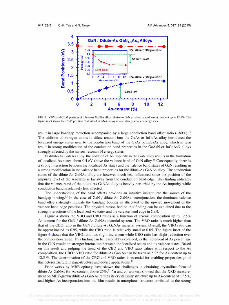
Figure 3 shows the valence band and conduction band alignment of dilute-As GaNAs alloywith respect to the GaN as a function of As-composition up to 12.5%. As the GaN alloy is takenas a reference, its valence band position is presumed at 0 eV while its conduction band position isset at 3.4 eV, constituting 3.4 eV energy band gap. When As impurity is introduced into GaN, theconduction band position is lowered down from 3.4 eV at 0%-As GaNAs to 3.346 eV at 12.5%-AsGaNAs, as shown in figure inset of figure 3. In our finding, the conduction band energy of dilute-AsGaNAs alloy is reduced by approximately 55 meV over the studied composition range from 0%to 12.5%-As. The corresponding valence band position raises up from 0 eV for 0%-As GaNAsalloy up to 1.15 eV for 12.5%-As GaNAs alloy. Based on the experimental measurement on theMBE-grown GaNAs alloy, Yu and co-workers reported the valence band position for the dilute-AsGaNAs alloy relative to GaN as 0.8 eV ± 0.3 eV from 2% to 10% of As-content in the alloy, and1 eV ± 0.3 eV with roughly 17.5% of As-content in the alloy.21 Our First-Principle findings are inreasonable agreement with the experimental data available in the literature.21
The discrepancies between our computed data and experimental results for the GaN / dilute-AsGaNAs alloy could mainly be caused by the strain effect existing in the grown alloy due to themuch larger atomic size of arsenic atom and also the formation of As-cluster and As-pair in thedilute-As GaNAs alloy. Note that our result is computed based on ideal and relaxed structure, andthe polarization field effects as well as charge transfer issue at the interface between GaN anddilute-As GaNAs alloy are not taken into consideration.
As shown in figure 3, the valence band offset is significantly larger than the conduction bandoffset for the GaN / dilute-As GaNAs material system. The results (figure 3) for dilute-As GaNAsalloy exhibit very distinct corresponding properties as observed in the dilute-nitride GaAsN / GaAsheterostructures.15 The incorporation of dilute amount of nitrogen (1-2%) in the GaAs or InGaAs
All article content, except where otherwise noted, is licensed under a Creative Commons Attribution 3.0 Unported license. See:
http://creativecommons.org/licenses/by/3.0/ Downloaded to IP: 207.172.231.174 On: Thu, 22 Jan 2015 14:23:22
017129-5 C.-K. Tan and N. Tansu AIP Advances 5, 017129 (2015)
FIG. 3. VBM and CBM position of dilute-As GaNAs alloy relative to GaN as a function of arsenic content up to 12.5%. Thefigure inset shows the CBM position of dilute-As GaNAs alloy in a relatively smaller energy scale.
result in large bandgap reduction accompanied by a large conduction band offset ratio (∼80%).15
The addition of nitrogen atoms in dilute amount into the GaAs or InGaAs alloy introduced thelocalized energy states near to the conduction band of the GaAs or InGaAs alloy, which in turnresult in strong modification of the conduction band properties in the GaAsN or InGaAsN alloysstrongly affected by the narrow resonant N energy states.
In dilute-As GaNAs alloy, the addition of As impurity in the GaN alloy results in the formationof localized As states about 0.4 eV above the valence band of GaN alloy.26 Consequently, there isa strong interaction between the localized As states and the valence band states of GaN resulting ina strong modification in the valence band properties for the dilute-As GaNAs alloy. The conductionstates of the dilute-As GaNAs alloy are however much less influenced since the position of theimpurity level of the As-states is far away from the conduction band edge. This finding indicatesthat the valence band of the dilute-As GaNAs alloy is heavily perturbed by the As-impurity whileconduction band is relatively less affected.
The understanding of the band offsets provides an intuitive insight into the source of thebandgap bowing.33 In the case of GaN / dilute-As GaNAs heterojunction, the dominant valenceband offsets strongly indicate the bandgap bowing as attributed to the upward movement of thevalence band edge positions. The physical reason behind this finding can be explained due to thestrong interactions of the localized As states and the valence band edge in GaN.
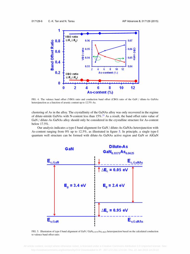
Figure 4 shows the VBO and CBO ratios as a function of arsenic composition up to 12.5%As-content for the GaN / dilute-As GaNAs material system. The VBO ratio is much higher thanthat of the CBO ratio in the GaN / dilute-As GaNAs material system. Overall, the VBO ratio canbe approximated as 0.95, while the CBO ratio is relatively small at 0.05. The figure inset of thefigure 4 shows that the VBO ratio has slight increment while CBO ratio has slight reduction overthe composition range. This finding can be reasonably explained, as the increment of As percentagein the GaN results in stronger interaction between the localized states and its valence states. Basedon this result and judging the trend of the CBO and VBO ratio values with respect to the Ascomposition, the CBO : VBO ratio for dilute-As GaNAs can be taken as 5:95 for As-content up to12.5 %. The determination of the CBO and VBO ratios is essential for enabling proper design ofthis heterostructure in nanostructure and device applications.42
Prior works by MBE epitaxy have shown the challenges in obtaining crystalline form ofdilute-As GaNAs for As-content above 25%.21 Yu and co-workers showed that the XRD measure-ment on MBE-grown dilute-As GaNAs retains its crystallinity structure up to As-content of 17.5%,and higher As incorporation into the film results in amorphous structure attributed to the strong
All article content, except where otherwise noted, is licensed under a Creative Commons Attribution 3.0 Unported license. See:
http://creativecommons.org/licenses/by/3.0/ Downloaded to IP: 207.172.231.174 On: Thu, 22 Jan 2015 14:23:22
017129-6 C.-K. Tan and N. Tansu AIP Advances 5, 017129 (2015)
FIG. 4. The valence band offset (VBO) ratio and conduction band offset (CBO) ratio of the GaN / dilute-As GaNAsheterojunction as a function of arsenic content up to 12.5%-As.
clustering of As in the alloy. The crystallinity of the GaNAs alloy was only recovered in the regimeof dilute-nitride GaNAs with N-content less than 15%.21 As a result, the band offset ratio value ofGaN / dilute-As GaNAs alloy should only be considered in the crystalline structure for As-contentbelow 17.5%.
Our analysis indicates a type-I band alignment for GaN / dilute-As GaNAs heterojunction withAs-content ranging from 0% up to 12.5%, as illustrated in figure 5. In principle, a single type-Iquantum well structure can be formed with dilute-As GaNAs active region and GaN or AlGaN
FIG. 5. Illustration of type-I band alignment of GaN / GaN0.9375As0.0625 heterojunction based on the calculated conductionto valence band offset ratio.
All article content, except where otherwise noted, is licensed under a Creative Commons Attribution 3.0 Unported license. See:
http://creativecommons.org/licenses/by/3.0/ Downloaded to IP: 207.172.231.174 On: Thu, 22 Jan 2015 14:23:22

017129-7 C.-K. Tan and N. Tansu AIP Advances 5, 017129 (2015)
barrier regions. The enhancement of the hole localization by using dilute-As GaNAs QW structureis expected to result in the increment of the exciton binding energy.35,43 However, the use of GaNbarriers will result in relatively weak electron confinement in the GaNAs QW. The use of AlGaNtensile barriers44 will potentially result in the strain compensation and improved barrier confinementin type-I GaNAs QW structure. In addition, the use of dilute-As GaNAs alloy had previously beensuggested in type-II InGaN / dilute-As GaNAs QWs27,28 for addressing the charge separation issuein the QW. The use of dilute-As GaNAs with large valence band offset in type-II QW structureresults in strong hole confinement, which in turn increase the electron-hole wavefunction overlap inpolar InGaN-based QWs resulting in improved spontaneous emission rate and optical gain.27,28
IV. CONCLUSIONS
In summary, the natural band alignment of dilute-As GaNAs / GaN heterostructure is deter-mined via First-Principle method. Our finding shows a type-I natural band alignment of dilute-AsGaNAs / GaN heterostructure, with the conduction to valence band offset ratio (CBO : VBO)determined as 5:95 for As-content up to 12.5%. The strong coupling of localized As-states is foundas the primary contributing factor in leading to the strong valence band modification resulting inthe bandgap reduction observed in the dilute-As GaNAs alloy. Future works on the impacts of theAs-clustering in the dilute-As GaNAs with high As-content on its band alignment with respect tothat of GaN will be important. The incorporation of dilute-As GaNAs alloy in the type-I or type-IIQW structures can result in significantly improved active regions for LEDs and lasers emitting inthe visible spectral regimes.
ACKNOWLEDGMENTS
The work was supported by US National Science Foundation (ECCS 1408051, ECCS 1028490,DMR 0907260), and the Daniel E. ’39 and Patricia M. Smith Endowed Chair Professorship Fund.The authors also acknowledge helpful technical discussions with Dr. Hannes Schweiger from Mate-rial Design. The authors also would like to acknowledge useful discussions with Dr. Benjamin O.Tayo, Dr. Jing Zhang, and Dr. Guangyu Liu, all from Lehigh University.1 S. Nakamura, Science 281, 956–961 (1998).2 M. H. Crawford, IEEE J. Sel. Top. Quantum Electron. 15, 1028-1040 (2009).3 H. Zhao, G. Y. Liu, J. Zhang, J. D. Poplawsky, V. Dierolf, and N. Tansu, Optics Express 19, A991-A1007 (2011).4 H. Zhao, G. Liu, R. A. Arif, and N. Tansu, Solid-State Electronics 54, 1119–1124 (2010).5 X. Li, S. Kim, E. E. Reuter, S. G. Bishop, and J. J. Coleman, Appl. Phys. Lett. 72, 1990-1992 (1998).6 X. Li, S. G. Bishop, and J. J. Coleman, Appl. Phys. Lett. 73, 1179–1181 (1998).7 X. Li, H. Liu, X. Ni, U. Ozgur, and H. Morkoc, Superlattices and Microstructures 47, 118-122 (2010).8 X. H. Li, R. Song, Y. K. Ee, P. Kumnorkaew, J. F. Gilchrist, and N. Tansu, IEEE Photon. J. 3, 489–499 (2011).9 I. H. Brown, P. Blood, P. M. Smowton, J. D. Thomson, S. M. Olaizola, A. M. Fox, P. J. Parbrook, and W. W. Chow, IEEE
J. Quantum Electron. 42, 1202–1208 (2006).10 H. Zhang, E. J. Miller, E. T. Yu, C. Poblez, and J. S. Speck, Appl. Phys. Lett. 84, 4644-4646 (2004).11 P. K. York, K. J. Beernink, G. E. Fernandez, and J. J. Coleman, Appl. Phys. Lett. 54, 499-501 (1989).12 N. Tansu, J. Y. Yeh, and L. J. Mawst, Appl. Phys. Lett. 82, 4038-4040 (2003).13 K. Uesugi, N. Morooka, and I. Suemune, Appl. Phys. Lett. 74, 1254-1256 (1999).14 L. Xu, D. Patel, C. S. Menoni, J. Y. Yeh, L. J. Mawst, and N. Tansu, Appl. Phys. Lett. 89, 171112 (2006).15 H.-P. Komsa, E. Arola, E. Larkins, and T. T. Rantala, J. Phys.:Condens. Matter 20, 315004 (2008).16 N. Tansu, J. Y. Yeh, and L. J. Mawst, IEEE J. Sel. Top. Quantum Electron. 9, 1220-1227 (2003).17 S. R. Bank, L. L. Goddard, M. A. Wistey, H. B. Yuen, and J. S. Harris, IEEE J. Sel. Top. Quantum Electron. 11, 1089-1098
(2005).18 A. Lindsay and E. P. O’Reilly, Phys. Rev. Lett. 93, 196402 (2004).19 C. G. Van de Walle and J. Neugebauer, Appl. Phys. Lett. 76, 1009–1011 (2000).20 A. Kimura, C. A. Paulson, H. F. Tang, and T. F. Kuech, Appl. Phys. Lett. 84, 1489-1491 (2004).21 K. M. Yu, S. V. Novikov, R. Broesler, C. R. Staddon, M. Hawkridge, Z. Liliental-Weber, I. Demchenko, J. D. Denlinger, V.
M. Kao, F. Luckert, R. W. Martin, W. Walukiewicz, and C. T. Foxon, Phys. Status Solidi C 7, 1847–1849 (2010).22 C. K. Tan, B. O. Tayo, J. Zhang, X. H. Li, G. Y. Liu, and N. Tansu, J. Disp. Technol. 9, 272-279 (2013).23 X. H. Li, H. Tong, H. P. Zhao, and N. Tansu, Proc. of the SPIE Photonics West 2010, Physics & Simulation of Optoelectronics
Devices XVIII, 75970H (2010).24 T. Mattila and A. Zunger, Phys. Rev. B 59, 9943-9953 (1999).
All article content, except where otherwise noted, is licensed under a Creative Commons Attribution 3.0 Unported license. See:
http://creativecommons.org/licenses/by/3.0/ Downloaded to IP: 207.172.231.174 On: Thu, 22 Jan 2015 14:23:22

017129-8 C.-K. Tan and N. Tansu AIP Advances 5, 017129 (2015)
25 K. Laaksonen, H.-P. Komsa, E. Arola, T. T. Rantala, and R. M. Nieminen, J. Phys.: Condens. Matter 18, 10097-10114(2006).
26 J. Wu, W. Walukiewicz, K. M. Yu, J. D. Denlinger, W. Shan, J. W. Ager III, A. Kimura, H. F. Tang, and T. F. Kuech, Phys.Rev. B 70, 115214 (2004).
27 R. A. Arif, H. Zhao, and N. Tansu, Appl. Phys. Lett. 92, 011104 (2008).28 H. Zhao, R. A. Arif, and N. Tansu, J. Appl. Phys. 104, 043104 (2008).29 M. Peressi, N. Binggeli, and A. Baldereschi, J. Phys. D: Apply. Phys. 31, 1273-1299 (1997).30 A. Baldereschi, S. Baroni, and R. Resta, Phys. Rev. Lett. 61, 734-737 (1988).31 L. Colombo, R. Resta, and S. Baroni, Phys. Rev. B 44, 5572-5579 (1991).32 N. R. D’Amico, G. Cantele, and D. Ninno, Appl. Phys. Lett. 101, 141606 (2012).33 P. G. Moses, M. Miao, Q. Yan, and C. G. Van de Walle, J. Chem. Phys. 134, 084703 (2011).34 P. G. Moses and C. G. Van de Walle, Appl. Phys. Lett. 96, 021908 (2010).35 L. Dong and S. P. Alpay, J. Appl. Phys. 111, 113714 (2012).36 S. H. Wei and A. Zunger, Appl. Phys. Lett. 72, 2011-2013 (1998).37 J. Robertson, J. Vac. Sci. Technol. B 18, 1785-1791 (2000).38 B. Hoffling, A. Schleife, C. Rodl, and F. Bechstedt, Phys. Rev. B 85, 035305 (2012).39 Material Designs Inc., Santa Fe, NM, USA, MedeA-VASP, http://www.materialsdesign.com.40 V. Fiorentini and A. Baldereschi, Phys. Rev. B 51, 11169-11186 (1996).41 P. W. Peacock and J. Robertson, Phys. Rev. Lett. 92, 057601 (2004).42 I. Vurgaftman and J. R. Meyer, J. Appl. Phys. 94, 3675-3696 (2003).43 D. A. B. Miller, D. S. Chemla, T. C. Damen, A. C. Gossard, W. Wiegmann, T. H. Wood, and C. A. Burrus, Phys. Rev. B 32,
1043-1060 (1985).44 H. P. Zhao, R. A. Arif, Y. K. Ee, and N. Tansu, IEEE J. Quantum Electron. 45(1-2), 66-78 (2009).
All article content, except where otherwise noted, is licensed under a Creative Commons Attribution 3.0 Unported license. See:
http://creativecommons.org/licenses/by/3.0/ Downloaded to IP: 207.172.231.174 On: Thu, 22 Jan 2015 14:23:22