finite state machines - university of torontoutsc.utoronto.ca/~bharrington/cscb58/labs/lab5.pdf ·...
TRANSCRIPT
CSC B58 - Lab 5Finite State Machines
Learning Objectives
The purpose of this lab is to learn how to create FSMs as well as use them to control a datapath over multipleclock cycles.
Marking Scheme
Prelab /3Part I (in-lab) /1Part II (in-lab) /3Clean work-space with all materials returned to their original state /1TOTAL /8
1

!"#$%&
'&
(&
Figure 1: Required timing for the output z.
Part I
We wish to implement a finite state machine (FSM) that recognizes two specific sequences of applied input sym-bols, namely four consecutive 1s or the sequence 1101. There is an input w and an output z. Whenever w = 1 forfour consecutive clock pulses, or when the sequence 1101 appears on w across four consecutive clock pulses, thevalue of z has to be 1; otherwise, z = 0. Overlapping sequences are allowed, so that if w = 1 for five consecu-tive clock pulses the output z will be equal to 1 after the fourth and fifth pulses. Figure 1 illustrates the requiredrelationship between w and z. A state diagram for this FSM is shown in Figure 2.
Figure 3 shows a partial Verilog file for the required state machine. Study and understand this code as it providesa model for how to clearly describe a finite state machine that will both simulate and synthesize properly.
The toggle switch SW0 on the DE2 board is an active-low synchronous reset input for the FSM, SW1 is the winput, and the pushbutton KEY0 is the clock input that is applied manually. The LED LEDR9 is the output z, andthe state flip-flop outputs are assigned to LEDR3−0.
2

!"#$
%"#$
&"#$
'"
#$
(")$
*"#$
+"
)$
,-.-/$
01)$
01)$
01)$ 01#$
01)$
01#$
01#$
01#$
01)$
01)$
01#$
01#$
01)$
01#$
Figure 2: A state diagram for the FSM.
3
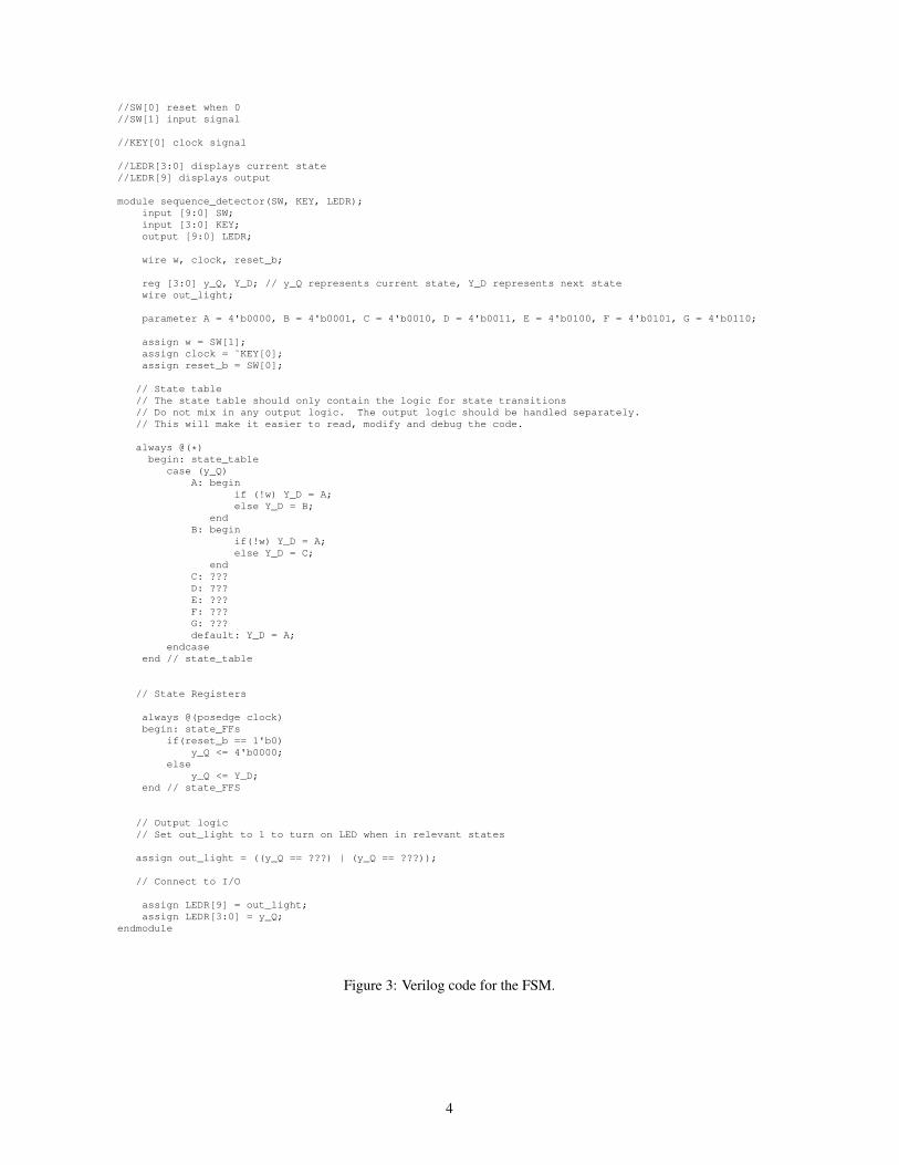
//SW[0] reset when 0//SW[1] input signal
//KEY[0] clock signal
//LEDR[3:0] displays current state//LEDR[9] displays output
module sequence_detector(SW, KEY, LEDR);input [9:0] SW;input [3:0] KEY;output [9:0] LEDR;
wire w, clock, reset_b;
reg [3:0] y_Q, Y_D; // y_Q represents current state, Y_D represents next statewire out_light;
parameter A = 4'b0000, B = 4'b0001, C = 4'b0010, D = 4'b0011, E = 4'b0100, F = 4'b0101, G = 4'b0110;
assign w = SW[1];assign clock = ˜KEY[0];assign reset_b = SW[0];
// State table// The state table should only contain the logic for state transitions// Do not mix in any output logic. The output logic should be handled separately.// This will make it easier to read, modify and debug the code.
always @(*)begin: state_table
case (y_Q)A: begin
if (!w) Y_D = A;else Y_D = B;
endB: begin
if(!w) Y_D = A;else Y_D = C;
endC: ???D: ???E: ???F: ???G: ???default: Y_D = A;
endcaseend // state_table
// State Registers
always @(posedge clock)begin: state_FFs
if(reset_b == 1'b0)y_Q <= 4'b0000;
elsey_Q <= Y_D;
end // state_FFS
// Output logic// Set out_light to 1 to turn on LED when in relevant states
assign out_light = ((y_Q == ???) | (y_Q == ???));
// Connect to I/O
assign LEDR[9] = out_light;assign LEDR[3:0] = y_Q;
endmodule
Figure 3: Verilog code for the FSM.
4

Perform the following steps:
1. Complete the state table and the output logic. (PRELAB)
2. Complete the template code provided online sequence_detector.v. (PRELAB)
3. Download the compiled circuit into the FPGA. Test the functionality of the circuit on your board and showyour TA
Part II
Most non-trivial digital circuits can be separated into two main functions. One is the datapath where the data flowsand the other is the control path that manipulates the signals in the datapath to control the operations performedand how the data flows through the datapath. In previous labs, you learned how to construct a simple ALU,which is a common datapath component. In Part I of this lab you have already constructed a simple finite statemachine (FSM), which is the most common component used to implement a control path. Now you will see howto implement an FSM to control a datapath so that a useful operation is performed. This is an important steptowards building a microprocessor as well as any other computing circuit.
In this part, you are given a datapath and also an FSM that controls this datapath and performs A2 + C.
Using the given datapath, you are required to implement an FSM that controls it to perform the computation:
Ax2 +Bx+ C
The values of x, A, B and C will be preloaded by the user on the switches before the computation begins.
Figure 4 shows the block diagram of the datapath you will build. Resets are not shown, but do not forget them.The datapath will carry 8-bit unsigned values. Assume that the input values are small enough to not cause anyoverflows at any point in the computation, i.e., no results will exceed 28 − 1 = 255. The ALU needs only toperform addition and multiplication, but you could use a variation of the ALU you built previously to have moreoperations available for solving other equations if you wish to try some things on your own. There are fourregisters Rx, RA, RB and RC used at the start to store the values of x, A, B and C, respectively. The registersRA and RB can be overwritten during the computation. There is one output register, RR, that captures the outputof the ALU and displays the value in binary on the LEDs and in hex on the HEX displays. Two 8-bit-wide, 4-to-1multiplexers at the inputs to the ALU are used to select which register values are input to the ALU.
All registers have enable signals to determine when they are to load new values and an active low synchronousreset.
The provided circuit operates in the following manner. After an active low synchronous reset on KEY0, you willinput the value for RA on switches SW [7 : 0]. When KEY1 is pushed and released, RA will be loaded and thenyou will input the next value on the switches that will be loaded into RB . Likewise for RC and RX . Computationwill start after KEY1 is pressed and released for loading RX . When computation is finished, the final result willbe loaded into RR. This final result should be displayed on LEDR7−0 in binary and HEX0 and HEX1 in hex. Youwill use CLOCK 50 as your clock.
5

C X A B
R
alu_select_a alu_select_b
ld_c ld_b ld_a ld_b
data_result
alu_op
ld_r
data_in
ld_alu_out
Figure 4: Block diagram of datapath.
Perform the following steps:
1. Examine the provided Verilog code. This is a major step in this part of the lab. You will not need to writemuch Verilog, but you’ll need to fully understand the provided Verilog in order to make your modifications.(PRELAB)
2. Modify the provided code to implement your controller and synthesize it. You should only modify thecontrol module. (PRELAB)
3. To examine the circuit produced by Quartus II open the RTL Viewer tool (Tools > Netlist Viewers > RTLViewer). Find (on the left panel) and double-click on the box shown in the circuit that represents the finitestate machine, and determine whether the state diagram that it shows properly corresponds to the one youhave drawn. To see the state codes used for your FSM, open the Compilation Report, select the Analysisand Synthesis section of the report, and click on State Machines.
The state codes after synthesis may be different from what you originally specified. This is because the toolmay have found a way to optimize the logic better by choosing a different state assignment. If you reallyneed to use your original state assignment, there is a setting to keep it.
4. After you are satisfied with your simulations, download and test the functionality of the circuit on the FPGAboard.
5. Demonstrate your correctly working code to your TA
6. Upload your .v files for all parts of this lab to Markus
6

Part III (Optional)
Division in hardware is the most complex of the four basic operations. Add, subtract and multiply are much easierto build in hardware. For this part, you will be designing a 4-bit restoring divider using a finite state machine.
Figure 5 shows an example of how the restoring divider works. This mimics what you do when you do longdivision by hand. In this specific example, number 7 (Dividend) is divided by number 3 (Divisor). The restoringdivider starts with Register A set to 0. The Dividend is shifted left and the bit shifted out of the left most bit ofthe Dividend (called the most significant bit or MSB) is shifted into the least significant bit (LSB) of Register A asshown in Figure 6.
Figure 5: An example showing how the restoring divider works.
7

Figure 6: Block diagram of restoring divider.
The Divisor is then subtracted from Register A. This is equivalent to adding the 2’s complement of the Divisor(11101 for the example in Figure 5) to Register A. If the MSB of Register A is a 1, then we restore Register A backto its original value by adding the Divisor back to Register A, and set the LSB of the Dividend to 0. Else, we donot perform the restoring addition and immediately set the LSB of the Dividend to 1.
This cycle is performed until all the bits of the Dividend have been shifted out. Once the process is complete, thenew value of the Dividend register is the Quotient, and Register A will hold the value of the Remainder.
To implement this part, you will use SW3−0 for the divisor value and SW7−4 for the dividend value. UseCLOCK 50 to for the clock signal, KEY0 as a synchronous active high reset, and KEY1 as the Go signal to startcomputation. The output of the Divisor will be displayed on HEX0, the Dividend will be displayed on HEX2, theQuotient on HEX4, and the Remainder on HEX5. Set the remaining HEX displays to 0. Also display the Quotienton LEDR.
Structure your code in the same way as you were shown in Part II.
Perform the following steps.
1. Draw a schematic for the datapath of your circuit. It will be similar to Figure 6. You should show how youwill initialize the registers, where the outputs are taken, and include all the control signals that you require.
2. Draw the state diagram to control your datapath.
3. Draw the schematic for your controller module.
4. Draw the top-level schematic showing how the datapath and controller are connected as well as the inputsand outputs to your top-level circuit.
5. Write the Verilog code that realizes your circuit.
6. Simulate your circuit with ModelSim for a variety of input settings, ensuring the output waveforms arecorrect.
7. After you are satisfied with your simulations, download and test the functionality of the circuit on the FPGAboard.
8