finite difference time-domain method for simulating
TRANSCRIPT

Digest Journal of Nanomaterials and Biostructures Vol. 15, No. 3, July - September 2020, p. 707 - 719
FINITE DIFFERENCE TIME-DOMAIN METHOD FOR SIMULATING
DIELECTRIC MATERIALS AND METAMATERIALS
A. HENDIa, F. ALKALLAS
a, H. ALMOUSSA
b, H. ALSHAHRI
b,
M. ALMONEEFa, M. ALENAZY
a, N. ALSAIF
a, A. ALTOWYAN
a,
A. LAREFb, M. AWAD
b, K. ORTACHI
b
aDepartment of Physics, College of Science, Princesses Nourah Bint Abdulrahman
University, Riyadh, Saudi Arabia bDepartment of Physics, College of Science, King Saud University, Saudi Arabia
In this study, Finite Difference Time Domain (FDTD) is employed to model and simulate
both dielectric materials and metamaterials. Interestingly, the metamaterials own very
peculiar characteristics that are related to the simultaneous negative permittivity and
permeability. Based on FDTD technique, we can simulate the electromagnetic devices
with the inclusion of the simultaneous electric and magnetic fields over time. The
striking features of metamaterials illustrate the increase and backward propagation as
well as the energy absorption in one-dimensional (1D) or two-dimensional (2D) systems.
These systems could have potential applications, such as metamaterial superlens.
(Received February 19, 2020, Accepted July 24, 2020)
Keywords: FDTD, Negative permittivity, Metamaterials, Superlens 1. Introduction During the past few years, a new technique for designing electromagnetic structures has
been suggested, where the electromagnetic waves could be modulated within a material by
incorporating the spatial variation in the constitutive parameters. The triggered notion of
metamaterials aroused a great deal of consideration of scientists for this kind of stimulating
applications in various frequency regimes from microwave, terahertz (THz), infrared (IR), optics,
and acoustics, etc. In aerospace functionalities, invisibility yields prohibiting information about an
object to attain radar-like detectors [1-6].
The Finite Difference Time Domain (FDTD) method, represents a powerful and an
effective technique that is extensively employed with successful manner for simulating and
modeling the electromagnetic wave interaction at different frequencies dispersion and non-
dispersed materials. In order to establish a new behavior, a manipulation through the dielectric and
magnetic response of a material is necessary. At this stage, it is feasible to involve metamaterials
as an effective medium tailored to acquire the desirable macroscopic characteristics via sub-
wavelength design. The prosperous fabrication of such metamaterials, emerged a prominent
consideration in the exploration of metamaterials by scientists from the diverse arenas. The
realization of metamaterials paved the pathway for various tremendous applications, such as
sub-wavelength imaging, solar cell design, and antennas [7-13].
The purpose of this work is to simulate the propagating electromagnetic waves both in
dielectric material and metamaterial (1D and 2D systems) by employing FDTD technique,
while the description of the method as well as the softwares that were used and changed
according to our simulated results, are provided in Refs. [13,14]. Also, we are mainly
concerned by involving the effect of varying the lattice cells in x-y directions, waveguides and
dielectric constants of the medium on the variation of propagating electromagnetic wave in 1D and
2D-systems.

708
2. Method of simulation: Finite Difference Time-Domain method
The FDTD is one of a commonly used technique for the solution of electromagnetic
problems. Both conceptually and in terms of implementation, it can accurately tackle a wide range
of problems even for programming three-dimensional systems. The FDTD method employs finite
differences as approximations to both the spatial and temporal derivatives that appear in
Maxwell’s equations (specifically Ampere’s and Faraday’s laws) [14].
2.1. FDTD in two dimensions
We will start with the Maxwell’s normalized equations [14]:
𝜕𝐷
𝜕𝑡=
1
√ԑ0 μ0 𝛻 × 𝐻 (1)
𝐷(𝜔) = ԑ𝑟 (𝜔) ∙ 𝐸(𝜔) (2)
𝜕𝐻
𝜕𝑡= −
1
√ԑ0 μ0 𝛻 × 𝐸 (3)
Here D is the electric flux density, H is magnetic field, E is the electric field, ԑ0 and μ0 are the permittivity and permeability in vacuum, and ԑ𝑟 is the relative permittivity. In a two-
dimensional simulation we need to choose between two modes: (1) the transverse magnetic
(TM) mode, which is composed of Ez, Hx, and Hy, or (2) transverse electric (TE) mode,
which is composed of Ex,Ey, and Hz. By using the TM modes, the equations above will be
reduced to:
𝜕𝐷𝑧
𝜕𝑡=
1
√ԑ0 μ0(
𝜕𝐻𝑦
𝜕𝑥−
𝜕𝐻𝑥
𝜕𝑦) (4)
𝐷𝑧(𝜔) = ԑ𝑟 (𝜔) ∙ 𝐸𝑧(𝜔) (5)
𝜕𝐻𝑥
𝜕𝑡= −
1
√ԑ0 μ0
𝜕𝐸𝑧
𝜕𝑦 (6)
𝜕𝐻𝑦
𝜕𝑡=
1
√ԑ0 μ0
𝜕𝐸𝑧
𝜕𝑥 (7)
To solve an electromagnetic problem, the idea is to simply discretize both in time and
space Maxwell’s equations with central difference approximations (see figure 1). In this cell
electric and magnetic components are distributed half time step shift and half special step shift in a
way that makes every single electric point surrounded by four magnetic points and vice versa [14].

709
T
Fig. 1. Interleaving for the two-dimensional TM formulation [14].
By plugging equations (4), (6),and (7) into the finite difference scheme results in:
𝐷𝑧𝑛+1/2
(𝑖,𝑗)−𝐷𝑧
𝑛−12(𝑖,𝑗)
𝛥𝑡=
1
√ԑ0 μ0
𝐻𝑦𝑛 (𝑖+1/2,𝑗)−𝐻𝑦
𝑛(𝑖−1/2,𝑗)
𝛥𝑥 −
1
√ԑ0 μ0
𝐻𝑥𝑛 (𝑖,𝑗+1/2)−𝐻𝑥
𝑛(𝑖,𝑗−1/2)
𝛥𝑥 (8)
𝐻𝑥𝑛+1 (𝑖,𝑗+1/2)−𝐻𝑥
𝑛(𝑖,𝑗+1
2)
𝛥𝑡= −
1
√ԑ0 μ0
𝐸𝑧𝑛+1/2
(𝑖,𝑗+1)−𝐸𝑧𝑛+1/2
(𝑖,𝑗)
𝛥𝑥 (9)
𝐻𝑦
𝑛+1 (𝑖+1/2,𝑗)−𝐻𝑦𝑛(𝑖.𝑗+1/2)
𝛥𝑡=
1
√ԑ0 μ0
𝐸𝑧𝑛+1/2
(𝑖+1,𝑗)−𝐸𝑧𝑛+1/2
(𝑖,𝑗)
𝛥𝑥 (10)
Equation (8) gives the temporal derivative of the electric flux density in term of the spatial
derivative of the magnetic field. Conversely, equations (9)-(10) provide the temporal derivative of
the magnetic field in terms of the spatial derivative of the electric field [2]. These two equations
represent a plane wave traveling in the z-direction [3]. Then it is possible to solve the resulting
difference equations to obtain "update equations that express the (unknown) future fields in terms
of (known) past fields. The magnetic fields are estimated one time-step into the future so they
are now known (effectively they become past fields), while the electric fields one time-step
into the future so they are now recognized (actually they become past fields). This procedure
can repeat the previous two steps until the fields have been obtained over the desired duration.
Where n is time t = 4t · n, the term n + 1 means one time step later, and the time step 4t
is defined by:
𝛥𝑡 =𝛥𝑥
2∙𝑐 (11)
Where c is the speed of light, and 4x is the cell size [14].
There are two cases for the determination of electromagnetic (EM) sources, such as the
generation of a continuous wave (CW) signal or a short pulse. Always there is a minimum
wavelength (maximum frequency) of interest. The cell size must be much smaller than minimum
wavelength.
There are typically two general classes of electromagnetic wave sources; the soft source
which consists of impressing a current and the hard source which consists of impressing an electric
field. The physical meaning of the soft source is well understood and its analytical solution is
known [14]. The source may be insert at any node (may be any value between first and
last node) by a time dependent source function g(t) (the soft source: Gaussian pulse ) as [14]:
g(t) = exp{−( t − t0
)2} (12)
710
t is the time delay and t0 indicates pulse width.
We employ in this simulation Gaussian source as source, as describe in Ref [14]. A
perfectly matched layer (PML) is commonly used to truncate the computational regions in
numerical methods to simulate problems with open boundaries, especially in the FDTD. A
PML is an artificial absorbing layer for wave equations, there are several equivalent
formulations of PML. ABCs creates a numerical representation that makes a grid with a finite
number of electric and magnetic field points to behave as if they were infinite. With these
conditions, the wave will be completely “absorbed” by the termination. If a wave is moving to a
boundary in free space, it is traveling by speed of light c0 in one time step in FDTD. The reason
for using PML is its effectiveness and versatility in working with different media [14-19].
Here the FDTD technique and the softwares that were modified according to our simulated
results, are represented in Refs. [13,14].
3. Results and discussion
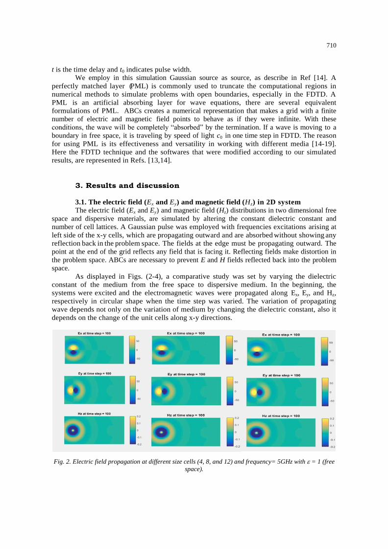
3.1. The electric field (Ex and Ey) and magnetic field (Hz) in 2D system
The electric field (Ex and Ey) and magnetic field (Hz) distributions in two dimensional free
space and dispersive materials, are simulated by altering the constant dielectric constant and
number of cell lattices. A Gaussian pulse was employed with frequencies excitations arising at
left side of the x-y cells, which are propagating outward and are absorbed without showing any
reflection back in the problem space. The fields at the edge must be propagating outward. The
point at the end of the grid reflects any field that is facing it. Reflecting fields make distortion in
the problem space. ABCs are necessary to prevent E and H fields reflected back into the problem
space.
As displayed in Figs. (2-4), a comparative study was set by varying the dielectric
constant of the medium from the free space to dispersive medium. In the beginning, the
systems were excited and the electromagnetic waves were propagated along Ex, Ey, and Hz,
respectively in circular shape when the time step was varied. The variation of propagating
wave depends not only on the variation of medium by changing the dielectric constant, also it
depends on the change of the unit cells along x-y directions.
Fig. 2. Electric field propagation at different size cells (4, 8, and 12) and frequency= 5GHz with = 1 (free
space).

711
Fig. 3. Electric field propagation at different thickness of layers ( =4) and frequency=5.GHz, unit cell=8
at different time steps.
Fig. 4. Electric field propagation at different thickness of layers ( = 8) and frequency=5.0 × 10 9 Hz, unit
cell=8 at different time steps.
3.2. The electric field (Ez) in two dimensional free space and dispersive
materials in 2D The electric field (Ez) in two dimensional free space and dispersive materials are
discussed with the alteration of the permittivity value () from free space to dispersive medium and the number of cells is varying in plane. To prohibit the reflections from lossy regions, the boundaries of absorbing grid is necessary for outgoing waves, by using perfectly matched layers. A Gaussian pulse was started in the center of cell along x-y directions by using PML. The cell size and number of step are varied to see their effect on the change of the propagating wave. The simulated results of the electric field along z-axis are displayed in figures (5-7) by changing the size cells along x-y directions and by varying the dielectric constant from free space to dielectric materials. The propagation of the wave nature at the central point is varied according to the variation of the thickness and medium when the time step is modified from the starting of the wave excitation until the absorption of the wave at the central region, which are determined at various dielectric constants. It is well noticed that the electric field at early time response is approximately the same at all different dielectric constants when the number of layers is equal to 100. However, the propagating wave is varying at the end of time step and this is due to the fact that the medium is more dispersive when the dielectric constant is increased.

712
Fig. 5. The electric field along z-direction versus x-y and = 1. Frequency=3 × 10⁷
Hz and number of
cells=100 at different time steps.
Fig. 6. The electric field along z-direction versus x-y and = 6. Frequency=3 × 10⁷
Hz and number of
cells=100 at different time steps.

713
Fig. 7. The electric field along z-direction versus x-y and = 8 Frequency=3 × 10⁷
Hz and number of
cells=100 at different time steps.
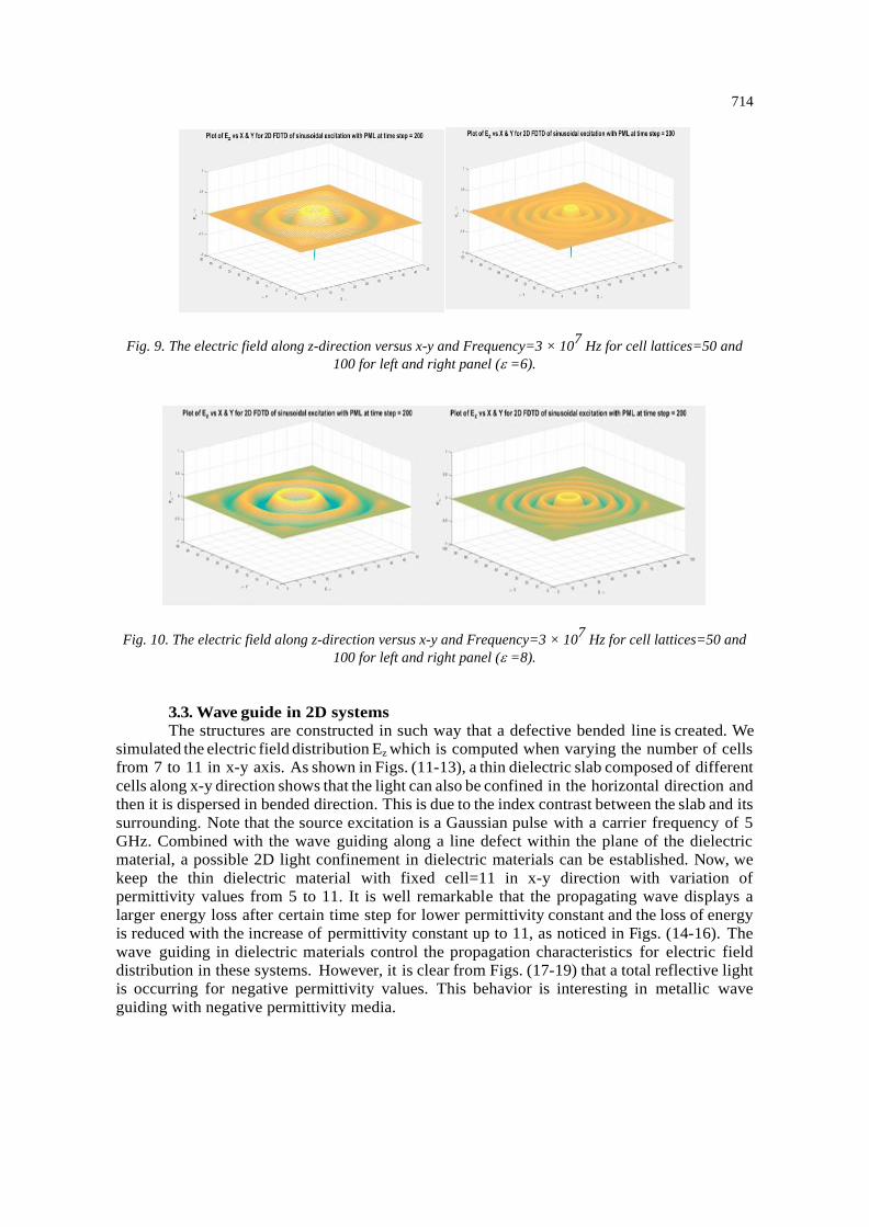
It is well remarkable from figures (8-10) with the increase of the thickness up to 100,
the wave propagation is changed in comparison with figures (5-7), even though keeping the
same values of permittivity (by varying them from free space to dielectric medium). Here the
time step is kept fixed for all cases.
Fig. 8. The electric field along z-direction versus x-y and Frequency=3 × 10⁷
Hz for cell lattices=50 and
100 for left and right panel ( = 1).
714
Fig. 9. The electric field along z-direction versus x-y and Frequency=3 × 10⁷
Hz for cell lattices=50 and
100 for left and right panel ( = 6).
Fig. 10. The electric field along z-direction versus x-y and Frequency=3 × 10⁷
Hz for cell lattices=50 and
100 for left and right panel ( = 8).
3.3. Wave guide in 2D systems The structures are constructed in such way that a defective bended line is created. We
simulated the electric field distribution Ez which is computed when varying the number of cells
from 7 to 11 in x-y axis. As shown in Figs. (11-13), a thin dielectric slab composed of different
cells along x-y direction shows that the light can also be confined in the horizontal direction and
then it is dispersed in bended direction. This is due to the index contrast between the slab and its
surrounding. Note that the source excitation is a Gaussian pulse with a carrier frequency of 5
GHz. Combined with the wave guiding along a line defect within the plane of the dielectric
material, a possible 2D light confinement in dielectric materials can be established. Now, we
keep the thin dielectric material with fixed cell=11 in x-y direction with variation of
permittivity values from 5 to 11. It is well remarkable that the propagating wave displays a
larger energy loss after certain time step for lower permittivity constant and the loss of energy
is reduced with the increase of permittivity constant up to 11, as noticed in Figs. (14-16). The
wave guiding in dielectric materials control the propagation characteristics for electric field
distribution in these systems. However, it is clear from Figs. (17-19) that a total reflective light
is occurring for negative permittivity values. This behavior is interesting in metallic wave
guiding with negative permittivity media.

715
Fig. 11. The electric field distribution along z-direction versus x-y number of cells=7 and = 11.4.
Fig. 12. The electric field distribution along z-direction versus x-y number of cells=11 and = 11.4.
Fig. 13. The electric field distribution along z-direction versus x-y number of cells=15 and = 11.4.
Fig. 14. The electric field along z-direction versus x-y for positive epsilon values ( = 5) and number of
cells=11 at different time step.

716
Fig. 15. The electric field along z-direction versus x-y for positive epsilon values ( = 7) and number of
cells=11 at different time step.
Fig. 16. The electric field along z-direction versus x-y for positive epsilon values
( = 11) and number of cells=11 at different time step.
Fig. 17. The electric field along z-direction versus x-y for positive epsilon values ( = −5) and number of
cells=11 at different time step.
Fig. 18. The electric field along z-direction versus x-y for positive epsilon values ( = −7) and number of
cells=11 at different time step.

717
Fig. 19. The electric field along z-direction versus x-y for positive epsilon values
( = −11) and number of cell=11 at different time step.
3.4. The electric field distribution for dielectric materials and metamaterials
In one dimensional case, the electric field distribution varies with the variation of time step
for the case of dispersive materials and metamaterials having positive and negative permittivity
which is analyzed using FDTD method, as displayed in figure 20. The frequency of operation is
given to be 0.7959 GHz for the purpose to provide a negative refractive index. The time step size
is selected in such way to be much smaller than the mesh density. The related time step is
computed by means of ∆(t) = 0.5, ∆ (x)/c, and c represents the speed of light. The metamaterial
cell is increased up to 100 cells. Outside this regime, the space is considered to be free space. The
absorbing blocks are centered at center to truncate the problem space. A sinusoidal source was
employed in the free- space regime. It is clear from Fig. 20 that the wave amplitudes in
metamaterials are significant than the normal free space, as well as of dispersive region. It is hence
the metamaterial increases the energy or intensity at the central regime. It is clear then the
absorbing energy is maximum from the surrounding media.
Fig. 20. Electric field distribution and transmission coefficient versus the frequency for positive epsilon
values ε2=2, and ε1=-2, 2, and 6 for left, middle, and right panels.
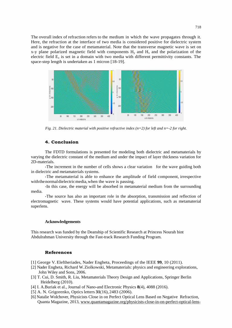
3.5. Positive refractive index in dielectric material and negative refractive in
metamaterials
The metamaterials are illustrating negative refractive index and own a characteristic not
occurring in conventional materials. For this reason, metamaterials underscore notable
capability for simplifying novel advancements in electromagnetism. In the case of one
dimensional, the medium is considered; where the metamaterial slab is inserted between the
two positive layers (ε > 0, μ > 0) layer. To formulate the metamaterial layer, the source
frequency is equal to 0.7959 GHz
Our simulations are performed for negative-refractive index (n=-2) metamaterial in
comparison with dielectric material having positive refractive index (n=2), as shown in figure 21.
718
The overall index of refraction refers to the medium in which the wave propagates through it.
Here, the refraction at the interface of two media is considered positive for dielectric system
and is negative for the case of metamaterial. Note that the transverse magnetic wave is set on
x-y plane polarized magnetic field with components Hy and Hx and the polarization of the
electric field Ez is set in a domain with two media with different permittivity constants. The
space-step length is undertaken as 1 micron [18-19].
Fig. 21. Dielectric material with positive refractive index (n=2) for left and n=-2 for right.
4. Conclusion
The FDTD formulations is presented for modeling both dielectric and metamaterials by
varying the dielectric constant of the medium and under the impact of layer thickness variation for
2D-materials.
-The increment in the number of cells shows a clear variation for the wave guiding both
in dielectric and metamaterials systems.
-The metamaterial is able to enhance the amplitude of field component, irrespective
with the normal dielectric media, when the wave is passing.
-In this case, the energy will be absorbed in metamaterial medium from the surrounding
media.
-The source has also an important role in the absorption, transmission and reflection of
electromagnetic wave. These systems would have potential applications, such as metamaterial
superlens.
Acknowledgements
This research was funded by the Deanship of Scientific Research at Princess Nourah bint
Abdulrahman University through the Fast-track Research Funding Program.
References
[1] George V. Eleftheriades, Nader Engheta, Proceedings of the IEEE 99, 10 (2011).
[2] Nader Engheta, Richard W. Ziolkowski, Metamaterials: physics and engineering explorations,
John Wiley and Sons, 2006.
[3] T. Cui, D. Smith, R. Liu, Metamaterials Theory Design and Applications, Springer Berlin
Heidelberg (2010).
[4] I. A.Buriak et al., Journal of Nano-and Electronic Physics 8(4), 4088 (2016).
[5] A. N. Grigorenko, Optics letters 31(16), 2483 (2006).
[6] Natalie Wolchover, Physicists Close in on Perfect Optical Lens Based on Negative Refraction,
Quanta Magazine, 2013, www.quantamagazine.org/physicists-close-in-on-perfect-optical-lens-

based-on-negative-refraction-20130808/.
[7] L. Billings, Nature 500, 138 (2013).
[8] K. Inoue, K. Ohtaka, Photonic Crystals Physics Fabrication and Applications, Springer Berlin
Heidelberg (2004).
[9] L. L. Lin, Z. Y. Li, K. M. Ho. J. Appl. Phys 94, 811 (2003).
[10] J. Joannopoulos et al., Photonics Crystal Modeling the Flow of Light, 2ed Ed. Princeton
University Press (2008).
[11] M. Maldovan, E. Thomas, Periodic Materials and Interference Lithography for Photonics,
Phononics and Mechanics, Wiley-VCH Verlag GmbH & Co (2009).
[12] Guy Vandenbosch, Computational Electromagnetics in Plasmonics, Plasmonics-
Principles and Applications. InTech, 2012.
[13] S. Rao, N. Balakrishnan, Computational Electromagnetics a Review (2013); Deshmukh R,
Marathe D, Kulat KD. Design of Multiband Negative Permittivity Metamaterial Based on
Interdigitated and Meander Line Resonator. In 2019 National Conference on Communications
(NCC) 2019 Feb 20 (pp. 1-6). IEEE; Sougata Chatterjee (2020). METAMATERIAL 1D
SIMULATION USING FDTD
METHOD (https://www.mathworks.com/matlabcentral/fileexchange/35530-metamaterial-1d-
simulation-using-fdtd-method), MATLAB Central File Exchange. Retrieved July 15, 2020; Soeren
Schmidt (2020). Interactive Simulation Toolbox for
Optics (https://www.mathworks.com/matlabcentral/fileexchange/40093-interactive-simulation-
toolbox-for-optics), MATLAB Central File Exchange. Retrieved July 15, 2020.
[14] Dennis M. Sullivan, Electromagnetic simulation using the FDTD method. John Wiley and
Sons, 2013.
[15] D. Markovich, K. Ladutenko, P. Belov, Progress in Electromagnetics Research 139,
655 (2013).
[16] Sevgi, Levent, Gelismis Arama. Electromagnetic modeling and simulation,
Computational Electromagnetics (ICCEM), 2015 IEEE International Conference on, IEEE,
2015.
[17] Fumie Costen, Jean-Pierre Bérenger, Anthony K. Brown, IEEE Transactions on Antennas and
Propagation 57(7), 2014 (2009).
[18] V. ShadrivovIlya, Andrey A. Sukhorukov, Yuri S. Kivshar, Physical Review E 67(5),
057602 (2003).
[19] George V. Eleftheriades, Nader Engheta, Proceedings of the IEEE 99, 10 (2011).