final report defense advanced research projects agency
TRANSCRIPT
Final Report
"All Solid-State Source Technology for TerahertzApplications"
June 2 0 th 2007
Sponsored by
Defense Advanced Research Projects Agency (DOD)(Controlling DARPA Office)
ARPA Order U051-72
Issued by U.S. Army Aviation and Missile Command Under
Contract No. W31P4Q-07-C-0111
Prepared by Dr. David Kurtz, Principle Investigator
Virginia Diodes Inc.979 Second Street SE
Suite 309
Charlottesville VA 22902434-297-3257
Effective Date of Contract: Dec 2 0 th, 2 0 0 6
Contract Expiration Date: Jun 2 0 'h, 2007Reporting Period: Dec 2 0 t', 2006-Jun 2 0 th, 2007
The views and conclusions contained in this document are those of the authors and should not beinterpreted as representing the official policies, either express or implied, of the Defense AdvancedResearch Projects Agency or the U.S. Government.
Approved for public release; distribution unlimited.

Table of Contents
List of Figures ........................................................... 3
List of Tables ............................................................ 4
Methods, Assumptions and Procedures ....................................... 5
Introduction ........................................................ 6
R eport .............................................................. 6
A. 660- 760 GHz Demonstrated and Delivered Source ............. 6
1. Physical Description ................................... 72. O peration .............................................. 9
a. Programming the Source ............................ 10L Synthesier .................................. 10iL Biasing .................................... 13
b. Feedback ......................................... 15
B. 797-83 7 GHz Transceiver ................................... 16
C. Measurement Results ........................................ 181. Tunable Power ...................................... 182. Spectral Purity ...................................... 183. Phase Noise ............................................ 194. Amplitude Stability ................................... 20
a. Noise ............................................. 20b. Drift .............................................. 21
Conclusion and Future Work ................................... 24
Sum mary .............................................................. 25
References ............................................................. 25
2

List of Figures
Figure 1: Pictures of the 660- 760 GHz source delivered for the contract ............ 7
Figure 2: Picture of the 660-760 GHz delivered source with control box ............. 8
Figure 3. Micro Lambda's timing illustration .............................. 11-12
Figure 4. Photograph of the 800 GHz transmitter .......................... 16
Figure 5: Photograph of 800 GHz receiver .................................. 17
Figure 6. 800 GHz transceiver: source power in red and conversion loss in blue .... 17
Figure 7: Source output power showing greater than 100 UWfrom 660-760 GHz .... 18
Figure 8: 800 GHz source phase noise for different RF and LOfrequencies, compared to20*Log(N) of the synthesizer phase noise .................................... 19
Figure 9: Drift for 800 GHz system with and without feedback ................... 22
Figure 10: Normalized output power of 800 GHz source showing change in power aftera heater changed the temperature by 2' C beginning at 100 s .................... 23
3

List of Tables
Table 1: DAQ and synthesizer pin connections ................................ 10
Table 2: Micro Lambda ' descriptions of the synthesizer ' digital lines ............. 11
Table 3: ASCII user commands with Micro Lambda's descriptions ................ 13
Table 4." Optimum bias values versus frequency for the D244 which is DAQ pin AO. 1 and
25-pin Dsub #8, and the D124 which is DAQpin AO.0 and 25-pin Dsub #7 ........ 14
Table 5: Component under feedback versus frequency. The data was determined with a
frequency resolution of 1.4 GHz ............................................ 15
4

Methods Assumptions and Procedures
Amplitude stability is defined based on the Electric field or Voltage waveforms.Percent rms is determined by converting all signals into a voltage waveform, calculatingthe mean, subtracting each measured data point from the mean, squaring the result,averaging all the squares which gives the variance, taking the square root of the variance,dividing by the mean, and multiplying by 100. Fluctuations slower than 10 Hz weremeasured by detecting the signal and measuring on a multimeter, or downconverting andmeasuring on an Agilent E4419B Power Meter with an E4413A head. Fluctuations fasterthan 10 Hz were measured by using a VDI WRI.2ZBD, zero bias detector, with anAD743 low noise operational amplifier. The amplified signal was measured on aTektronix TDS 744 oscilloscope with AC coupling. The WRI.2ZBD was operated in thelinear region, and the DC detected voltage was assumed to represent the voltageamplitude of the RF signal.
Frequency was measured using an HP5343A frequency counter.
Output powers for this report were measured using an Erickson WRI0 power meter.The manufacturer estimates the measurement uncertainty to be 5%. The input waveguideis wrlO, but the meter also accurately measures higher frequencies. A waveguide taperwas used to transition from the waveguide of the device under test to the wr !0 waveguideof the power meter. The loss of these tapers varies from 3-33% depending on thefrequency. The output power reported here was calibrated based on the taper's insertionloss according to the following table.
Frequency (GHz) Linear factor
180 1.03
225 1.06
550 1.24
700 1.33
Phase noise was measured by first downconverting and measuring total sideband poweron the HP8565E Spectrum Analyzer. It's assumed that this measurement represents aworst case.
5

I. IntroductionExisting and emerging applications for terahertz technology motivate the need for
improved terahertz sources. With the Submillimeter-wave technology gap, terahertzsources lag the performance found in other regions of the spectrum. Many applicationssuch as imaging, chemical agent detection, and spectroscopy would benefit fromnarrowing the technology gap. This SBIR focuses on improving key aspects of terahertzsources including power, spectral purity, and noise while maintaining good bandwidth,sweep speed, and size for output frequencies from 0. 1-1 Terahertz.
For the interim technical report, Virginia Diodes Inc. (VDI) reported power andbandwidth results for two different sources. One source uses all broadband componentsto achieve the maximum bandwidth, while the other source uses a mixture of highpowered and broadband components to achieve the maximum amount of power over 100GHz of bandwidth. VDI has delivered the high powered version for completion of phaseI. The source operates from 660-760 GHz with greater than 100 1aW of power. Thesource meets or exceeds the phase I objectives in all regards except amplitude stability.The amplitude stability of the source exceeds VDI's expectations of what could beaccomplished in phase I and has been thoroughly analyzed to determine how to meet thespecification for phase 2. The source is lightweight, compact, and easy to use. It can beswept across the band rapidly under full computer control.
The source uses a synthesizer to achieve very high spectral purity. The synthesizerwas delivered to VDI from Micro Lambda Wireless Inc. very late in the contract, soanother similar source operating around 800 GHz was used for many of themeasurements. The 800 GHz source, discussed in section B, was developed for anotherproject, but has similar components. Most importantly, the source was made with acompatible receiver that was indispensable for measuring phase noise and searching forspurious signals. Developing a receiver specifically for this contract could not have beendone within the time frame, but the performance of the 800 GHz source is most likelyvery similar to the delivered source. So, measurements that could not have been donewith the 660-760 GHz source without a receiver were done with the 800 GHz transceiver.Some of the measurements reported here were made with the 800 GHz source and somewere made with the 660-760 GHz delivered source. The delivered source is described indetail including all the necessary information to allow user programming of the sourcefor incorporation into any measurement system. The performance of the source isthoroughly analyzed and reported in the measurement results section.
II. Report
A. 660-760 GHz Demonstrated and Delivered Source
A terahertz source was developed and delivered that produces greater than 100 jiWtunable from 660-760 GHz. The performance of this source was characterized in termsof phase noise, amplitude stability, spurious frequencies, spectral purity, sweep speed,power, and bandwidth. The performance exceeds the Phase 1 requirements in all areasexcept amplitude stability. The amplitude stability requirement is the most challenging,
6

and though this source does not meet that requirement it exceeds VDI's expectations ofwhat could be accomplished in Phase 1, and we have identified many of the obstacles thathopefully can be overcome to exceed the specification in Phase 2. The following sectionsdescribe the physical layout and operation of this source.
1. Physical Description
The source uses an all solid-state, amplifier multiplier chain (AMC) produced byVDI to multiply the frequency of a YIG-based synthesizer, MLSE-0220, from MicroLambda Wireless [1]. The synthesizer is phase locked to a low phase noise, 10 MHz,crystal oscillator produced by Wenzel Associates Inc [2]. The crystal oscillator,synthesizer, and AMC are mounted together on an aluminum plate resulting in a compact(0.0062 in 3 ), lightweight (8.2 Ibs), terahertz source as shown in Figure 1. The AMC uses3 VDI multipliers and a Spacek active doubler to multiply the synthesizer frequency by afactor of 48 [3]. The Spacek active doubler provides about 2 Watts from 27-32 GHz anddrives a VDI Q120 which quadruples the frequency to give about 100-200 mW. TheQ 120 includes two doublers in one block housing similar to the VDI doublers named D60and D124. Next, a VDI D244 doubles the frequency to drive a WRI.2x3 broadbandtripler which is the final stage to bring the output frequency to 660-760 GHz.
e - 0
Figure 1: Pictures of the 660-760 GHz source delivered for the contract.
7

The source receives DC power, multiplier bias, and digital control of the synthesizerthrough one 9-pin D-sub and one 25-pin D-sub connector conveniently located on theedge of the plate as shown in Figure 1. For added convenience and ease of use, a controlbox (0.016 M3 , 14 Ibs) is included that plugs into a wall power outlet and with a singleswitch provides all the necessary DC voltages to run the source. Furthermore, acomputer can communicate with the control box through a USB connector to control theoutput frequency. A CD is included which installs a program for fast and easy frequencycontrol. A picture of the entire system including a laptop computer is shown in Figure 2.
4 1
Figure 2: Picture of the 660-760 GHz delivered source with control box.
A feedback control circuit and bias circuit are also housed on the Aluminum plate toprovide the optimum multiplier bias and output power control of the Spacek amplifier toachieve the maximum possible output power and bandwidth without damaging themultipliers. This circuit provides a knob which manually controls the source's outputpower along with two BNC connectors that allow voltage variable attenuation (VVA) andTTL amplitude modulation.
The output power can be precisely controlled by applying a voltage on the VVAport. A 5 V signal on the VVA connector completely attenuates the output power, and 0V provides no attenuation. The modulation port completely attenuates the output power
8

for all voltages greater than 2.5 V and has no effect for all voltages less than 2.5 V. TheVVA port could be used to amplitude modulate the source, but there is an initialovershoot for fast changes that occur before the feedback circuit can adjust. The TTLmodulation port allows modulation with no overshoot, but allows only an on and an offstate.
The setup procedure is simple and short:
1. Attach the cables between the control box and the source plate.2. Install the program on a computer.3. Plug the control box into a wall outlet.4. Attach the USB cable between the computer and the control box.5. Allow the computer to automatically install the hardware.6. Turn on the control switch.7. Run the program to set the output frequency.
The output power radiates into free space through a diagonal horn antenna shown inFigure 1. There is a directional coupler between the synthesizer and the Spacek amplifierthat allows the user to sample the synthesizer output power in order to verify operation.Also, there is an SMA T connector on the 10 MHz crystal oscillator to access the 10 MHzsignal for phase locking together multiple instruments with the source such as afrequency counter, spectrum analyzer or a VDI receiver.
The program installation disc will install NI-DAQ 8.5 Runtime 4. This distributioncontains all the features in the full NI-DAQmx version except for ADE support forLabVIEW, LabWindows/CVI and Measurement Studio, the DAQ Assistant, the NI-DAQmx documentation, and Real-Time Support. Installation of NI-DAQ 8.5 will resultin the removal of all previous versions of NI-DAQmx currently installed. Additionally,NI-DAQ 8.5 only supports LabVIEW version 7.1 and later. All NI-DAQmx support inprevious versions of LabVIEW will be removed. The full version of NI-DAQ 8.5, can bedownload from www.ni.com.
This section described the physical layout, purpose, and use of each component inthe source. The next section describes how the source operates along with allinformation necessary to program the source.
2. Operation
The source's output frequency and power can be computer controlled to achievegreater than 100 piW from 660-760 GHz without any mechanical tuning thus resulting invery fast fully optimized frequency sweeps. As described in the physical layout section,a Spacek amplifier and VDI multipliers are used to multiply the frequency output of asynthesizer by a factor of 48. A computer controls the synthesizer frequency andmultiplier bias, and a feedback circuit regulates the Spacek amplifier output power toachieve maximum bandwidth, power, and sweep speed without damaging the multipliers.Understanding how the computer controls the synthesizer and multiplier bias is notimportant for operating the source and setting up frequency sweeps. However, often thesource will need to be used within a system with a receiver or power meter, and the
9

system components must be controlled together. In other words, depending on theapplication it may be necessary to program the source, and the following information inthis report may serve as a user manual with all the necessary information.
a. Programming the Source
i Synthesizer
The computer controls a National Instruments USB-6221 Data Acquisition device(DAQ), and the DAQ controls the Synthesizer and multiplier bias [4]. The synthesizercommunicates using 6 digital lines. These 6 lines are connected to digital input andoutput pins of the DAQ according to Table I. The synthesizer responds to the ASCIIcommands shown in Table 3. The DAQ sends an ASCII command in serial binaryformat, most significant bit first, over the "DATA" line. Each bit is read with each risingedge of a pulse on the "CLOCK" line only when the "ENABLE" line is set to low (OV).Synthesizer responses are received on the falling edge of the clock pulse. Table 2 andFigure 3 are from Micro Lambda's instructions which provide timing, handshaking, andother information.
DAQ Pin Name 25-pin connector pin # 20-pin Synthesizer pin # Synthesizer Line NameP0.0 3 9 CLOCKP0. 1 2 10 DATA INP0.2 4 11 ENABLEP0.3 11 12 BUSYP0.4 13 14 LOCK ALARMP0.5 15 13 DATA OUT
Digital GND 18 4 LOGIC GNDTable 1: DAQ and synthesizer pin connections.
Select Input Active Low. Enables the shifting of data into the internalcommand buffer. Also serves as a command terminatorwhen it goes HIGH. The status of the BUSY line should bechecked before activating this line.
Clock Input Data is clocked into the unit on the rising edge (PositiveEdge Clocked) and Data Out is valid at this time. Themaximum clock rate of this line is 50 usec. For bestperformance the status of the DataOut line should bechecked before sending the first Clock. This line should bemaintained in a LOW state at the application of Select toprevent confusion.
Data In Input Input data pin. Data is sent MSB first. Data must be stable50 usec. Before the Clock line goes high and 50 usec.After the clock goes low. (Setup / Hold time)
10

BUSY Output This line is used to indicate that the unit is busy processingother commands or doing its internal housekeeping. Beforesending a Select = TRUE the status of this line should bechecked to ensure that it is LOW (NOT Busy). Anycommand initiated by setting Select Low while BUSY isHigh may result in lost data and uncertain results. NOTE:The unit can be programmed without using this line ifsufficient time is allowed between Clocks and betweencommands. The time required varies between commands.This mode is not recommended as there are some eventsthat occupy the microcontroller other than the serialcommunications.
DataOut Output This line is used to pass internal status information fromthe synthesizer. Data is guaranteed to be valid on thefalling edge of the clock signal. Data is sent out MSB first.In addition, this line is used as a communication'handshake' line. Once Select has gone LOW the DataOutline will be taken HIGH to indicate that the unit islistening. It will remain HIGH until the first data is sent outwhich is initiated by the first rising edge of Clock. DataOutwill be returned to LOW after Select has been released.
Table 2: Micro Lambda's descriptions of the synthesizer's digital lines. In additionto the lines above there is a unit status line, LOCK Status, which is a static linewhich only indicates the overall health of the unit - specifically, that all of theinternal phase locked loops are locked.
I I
TCH
TCL
I I
Dat a iv I
Dat aOLA

i)
Busy NotVa[W
Figure 3: NMicro Lambda's timing illustration. Tsc > 2 usec select low before firstclock, Tcs > 2 usec clock low before chip select high, Tsu > 2 usec data stable beforerising edge of clock, Tch > 2 usec minimum clock high time, Tcl > 2 usec minimumclock low time, Tsb > lOusec (time to wait before sampling 'BUSY' Data and Clocksetup / hold time = 10 usec. {hold time is determined from Tch}
Command DescriptionReports Status of all internal phase locked loops; threeloops are indicated by bits 0, 2, and 3. The other bits areinternal variables with of no particular interest to theuser.
> Recalls the synthesizer state from the next sequentialsaved memory location. If the last location accessed wasthe 99th, the '>' would recall the 100th location. Usingthis command the user can get the maximum step ratefrom the unit. (Used in conjunction with the NRcommand only.)
AX Enables the auxiliary RF input port J6. This will allowan external frequency, within the frequency range of theunit (applied to J6) to be passed to the main RF outputconnector J5. AXO = Disable, AXI = Enable. Note:AX I command disables the internal synthesizer output.This mode is an option.
f Frequency command (binary). The ASCII 'f' isfollowed by 34 bits of frequency data. The data is instraight binary format with the LSB representing I Hz.(i.e. 3.456789012 GHz would be commanded byfool0100110000010100110101000010100 ('ffollowed by CEOA6AI4 Hex)
F Frequency command (ASCII). This accepts thefrequency in MHz in straight ASCII format. i.e.3.456789012 GHz would be commanded byF3456.789012
L Sets the LOCK ALARM output polarity; L I sets theunit for LOCK = positive true; LO sets the unit forLOCK == negative true. (pin 13 of J1; Lock Alarm)
NR Recalls a synthesizer state from the specified location.(one of 1000 saved using the NS command) 'NR'followed by a hex address of 0x0063 would recall theinstrument state stored in the 99th decimal location.
12
NS Stores the present state of the synthesizer in thespecified location. (one of 1000 available); 'NS'followed by a hex address of 0x0064 would store thepresent state of the synthesizer in the 100th (decimal)location.
PL RF Power Level command. It is used to set the RFoutput level within the usable range of the unit,typically -20.0 to +20.0 dBm. This command acceptsthe RF power level setting in dBm. The characters are inASCII format. i.e. +19.5 dBm setting would becommanded by PL+ 19.5 and -10.1 dBm would be PL-10.1. (Available with the RF Power control optiononly.)
R Programs the Reference frequency. Range 5 to 50 MHz;1 MHz resolution. eg. R25.0 would set the externalreference frequency to 25 MHz.
SP Synthesizer Preset - Clears all nonvolatile memorysettings to factory default. Typically used to clearerroneous settings in the unit.
T Reads internal temperature information. Responds withdegrees C in a one byte response (signed char). Range: -40 to +80; Note: Since the T command is only one byte
long and the command needs to be processed before theunit can acquire the temperature data, the data returnedis always one command behind. Thus if you want thepresent temperature the T command should be senttwice and the second data used.
VF Programs the secondary VCO frequency synthesizer(second LO opt., J3) frequency. The characters are sentin ASCII format. i.e. VFI000.0 would set thesynthesizer 2nd output PLL for 1000.0 MHz
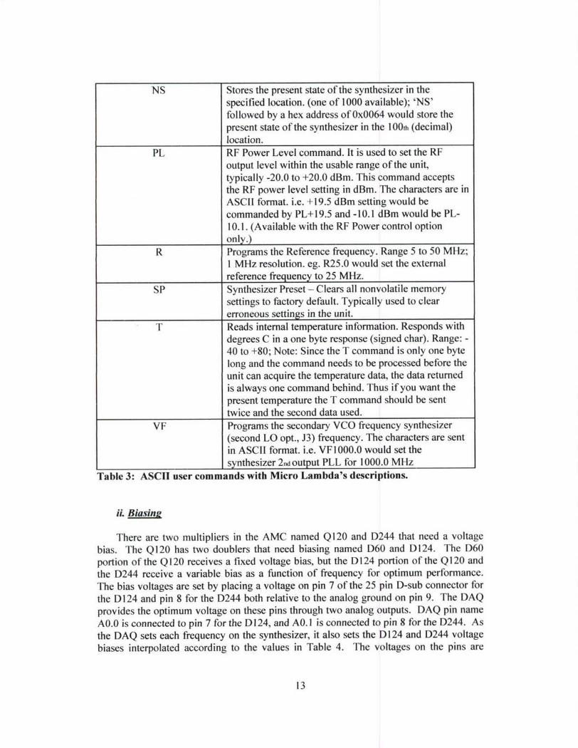
Table 3: ASCH user commands with Micro Lambda's descriptions.
i. Biasmng
There are two multipliers in the AMC named Q120 and D244 that need a voltagebias. The Q120 has two doublers that need biasing named D60 and D124. The D60portion of the Q120 receives a fixed voltage bias, but the Dl124 portion of the Q 120 andthe D244 receive a variable bias as a function of frequency for optimum performance.The bias voltages are set by placing a voltage on pin 7 of the 25 pin D-sub connector forthe D124 and pin 8 for the D244 both relative to the analog ground on pin 9. The DAQprovides the optimum voltage on these pins through two analog outputs. DAQ pin nameAO.0 is connected to pin 7 for the D 124, and AO. I is connected to pin 8 for the D244. Asthe DAQ sets each frequency on the synthesizer, it also sets the D124 and D244 voltagebiases interpolated according to the values in Table 4. The voltages on the pins are
13

amplified with maximum and minimum limits, so that the pin voltages are not the sameas the multiplier bias voltages. Also, the DAQ cannot output enough voltage to damagethe system, so a programmer cannot cause damage with programming errors. The inputimpedance for both pins 7 and 8 is 15 Kohms.
Frequency(GHz) D244 DAQ Output Bias (V) D124 DAQ Output Bias (V)630 -4.137 -7.715
634.2 -4.182 -5.915638.4 -4.187 -7.795642.6 -3.907 -4.395646.8 -3.217 -3.195
651 -3.312 -1.819655.2 -3.847 -0.003659.4 -3.907 0.147663.6 -3.657 0.097667.8 -3.032 0.177672 -3.887 0.177
676.2 -4.157 0.177680.4 -3.787 -5.817684.6 -3.372 -6.619688.8 -3.237 -6.077693 -3.112 -4.868
697.2 -2.967 -2.627014 -2.997 -0.67705.6 -3.147 -0.419709.8 -3.157 -1.005714 -2.887 -2.715
718.2 -2.797 -0.112722.4 -2.827 0.177726.6 -2.557 0.107730.8 -2.797 0.077735 -3.312 0.077
739.2 -3.507 0.077743.4 -3.252 0.077747.6 -2.827 0.097751.8 -2.497 0.177756 -3.489 0.177
760.2 -3.491 0.177764.4 -3.026 0.177768.6 -2.505 0.177770 -2.331 0.177
Table 4: Optimum bias values versus frequency for the D244 which is DAQ pinAO.1 and 25-pin Dsub #8, and the D124 which is DAQ pin AO.0 and 25-pin Dsub #7.
14

b. Feedback
A feedback circuit maintains safe power levels by limiting the RF generated DCcurrents in the multipliers. DC currents are generated by the multipliers when exposed toRF power. The currents are typically proportional to power levels and can be used as arough metric for RF power in the device. Through various tests, VDI has determinedsafe operating currents. The lifetime of the multiplier is reduced when RF powerproduces generated DC currents above the safe level. RF power can be controlled bycontrolling the output power of the Spacek amplifier. Spacek allows access to thetransistor drain of their amplifiers through a pin called "Psat", so that the voltage on Psatdirectly controls the output power. The feedback circuit continually monitors the DCgenerated currents and decreases the voltage on Psat to reduce the RF power if thecurrents exceed safe limits. The circuit responds faster than a millisecond, so safe levelsare restored before the multipliers reach dangerous temperatures. The Q120 and theD244 are monitored by the feedback circuit, but likely only one will reach the limit at atime. If there is not enough RF power for any of the multipliers to reach a limit then thefeedback circuit does nothing. Therefore, the system will not be under feedback for allfrequencies. Also, the D244 will limit the power at some frequencies while the Q120will limit the power at other frequencies. Table 5 shows the feedback status of thedelivered source as a function of frequency. The effects of feedback on amplitudestability have been explored and are described in the measurement results section.
Frequency Range (GHz) Component Under Feedback630-654 D60654-658 D244
658-667.8 D60667.8-670.6 D244670.6-696 D60696-700 D244700-730 D60730-770 NONE
Table 5: Component under feedback versus frequency. The data was determinedwith a frequency resolution of 1.4 GHz
15

B. 797-83 7 GHz Transceiver
The synthesizer for the delivered source did not arrive until very late in the contract;therefore, an 800 GHz transceiver with similar components to the delivered source wasused to complete many of the measurements for this contract such as phase noisemeasurements and searches for spurious harmonics. Also, a receiver was not availablefor the delivered source, but was available for the 800 GHz source which likely hassimilar performance to the delivered source. A picture of the source and receiver isshown in Figure 4 and Figure 5. The source uses a synthesizer from Micro Lambda,MLSN-1012, a Spacek active tripler, A369-3XWB-24, a VDI D70, D142, and D280frequency doublers, and a VDI WRI.2x3 frequency tripler. The receiver uses a Spacekactive doubler, A246-2XWB-31, a VDI DIOOV3, D200R2, and D400 frequencydoublers, and a WRI.2SHM sub-harmonic mixer. The source's output power and thereceiver's conversion loss are shown in Figure 6.
Figure 4. Photograph of the 800 GHz transmitter.
16
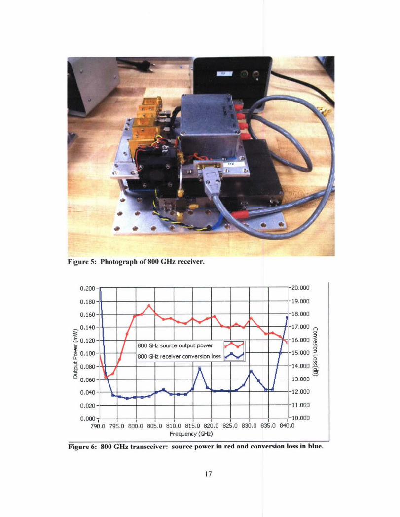
Figure 5: Photograph of 800 GHz receiver.
0.200------------------------- --- 20a000
0,160- 1.0
0
E_ -. 120 -- __ -16.000~
800 GHz receiver conversion loss0
0 0__00_1.00
0.020- - -11.--1 . 000
0,
0 0 0 -- I I I I -I-10.000790.0 795.0 800.0 805,0 810.0 815,0 820.0 825.0 830.0 835.0 840.0
Frequency (GHz)
Figure 6: 800 GHz transceiver: source power in red and conversion loss in blue.
17

C. Measurement Results
1. Tunable Power
The delivered source gives power from 630-760 GHz with greater than 100 pW from660-760 GHz as shown in Figure 7. The program can sweep the source across thebandwidth using any number of discrete points. The program takes about 25 ms perpoint, but the synthesizer takes 32 ms to change frequencies, so a 1000 point sweepacross the band takes 32 seconds.
0.280-
0.260- 0 a.
0.240- i
0.220- r ~
0.200-3ý0. 180 - ___
Z' 0.160-00.140-V-~0.120-1
I#
"0.10S0.100-
0.040-
0.020-0.000- _ __
620.0 640.0 660.0 680.0 700.0 720.0 740.0 760.0 780.0Frequency (GHz)
Figure 7: Source output power showing greater than 100 jiW from 660-760 GHz
2. Spectral Purity
The synthesizer has a resolution of I Hz. The frequency multiplication factor is48, therefore the output frequency resolution is 48 Hz. Sometimes, sources have powerat unwanted frequencies called spurs. Spurs can appear for some input frequencies anddisappear at others. A frequency selective power measurement from 660-760 GHz isnecessary to measure spurs. Typical spectrum analyzers with extenders barely reachabove 300 GHz, and even with state of the art microwave equipment, exhaustive spursearches can be very time consuming.
Perhaps the most effective way of searching for spurs is to use a 660-760 GHzreceiver to downconvert the source's output within the range of a 50 GHz spectrumanalyzer. Building a Terahertz receiver for this was not within the time frame of this
18

Phase 1, however a transceiver at 800 GHz with very similar components but lessbandwidth was under development for another customer, and this system was used tomake measurements for this contract. The 800 GHz receiver downconverted the source'soutput power to be measured on an HP8565E Spectrum Analyzer. The Local Oscillatorof the receiver was fixed while the RF was swept across the band. There were no spursfound in the source within the noise floor of the Spectrum analyzer which was about 20-40 dB below the IF signal.
3. Phase Noise
Phase noise was measured using the 800 GHz transceiver with a spectrum analyzer.The 800 GHz output was downconverted by mixing with a local oscillator and thenmeasured on a spectrum analyzer. Theory predicts that the output phase noise should begreater than the crystal oscillator by 20*Log(N) where N is the harmonic number. Figure
8 shows the comparison between measured and predicted phase noise for the 800 GHz
system for different RF and LO frequencies. The spectrum analyzer cannot distinguishbetween amplitude noise and phase noise or between transmitter, receiver or analyzernoise. So, the plots in Figure 8 show the worst case scenario.
-25,000-~ ____
S30GHz IF, 840GHz RF, 810GHz LO
35.00 1 GHz IF, 839GHz RF, 840GHz LO-35,.000 -
-40,000- L• 10GHz IF, 820GHz RF, 810GHz LO
I GHz IF, 811GHz RF, 810GHz LOM -45,000- -":a___ 20Log(N) of synthesizer sideband noise
-50.000- - _ _ _ _ _ _ _ _ _ __
Z -55.000--
-60.000 - _ ____ _ _ , ____
Ln -65,000- -__
-70.000- - __
-75.000-- _ __
-80.000--
-85 .000-0.0 10,0 20.0 30.0 40.0 50.0 60.0 70.0 80.0 90.0 100.0 110.0
Frequency Offset (KHz)
Figure 8: 800 GHz source phase noise for different RF and LO frequencies,
compared to 20*Log(N) of the synthesizer phase noise.
19

4. Amplitude Stability
Amplitude stability is the most challenging specification for this contract. Variousnoise sources such as thermal noise, phase noise, and ground loop noise cause smallfluctuations in the output power. These fluctuations can occur very rapidly or veryslowly. The rapid fluctuations represent noise contributions whose frequencies are largecompared to the sweep rate. The noise can be filtered or averaged by measuring overmany cycles of the noise at each output frequency. The amount of time to average ateach point can be determined by the amount of desired noise reduction and the noisepower spectral density. Long averaging times would be necessary to achieve highstability in the presence of low frequency noise power.
At some point, the output power fluctuations occur so slowly or non-cyclically thataveraging or filtering is not effective or results in excessively long time constants. Theseslow fluctuations are often described as "drift". In this report, amplitude stability isdivided into two categories: noise and drift, where noise represents fluctuations thatoccur faster than 10 Hertz and drift represents fluctuations that occur slower than 10Hertz. The methods for measuring and solutions for minimizing these two types offluctuations are different. Ten Hertz is the dividing frequency because it is the lowfrequency limit for the technique used to measure the noise described in the followingsection. The feedback circuit used to maintain safe operating power levels is effective forreducing both noise and drift, so the following sections describe the differences in noiseand drift with and without feedback.
a. Noise
The voltage amplitude stability in regards to noise fluctuations for this source is lessthan 0.045% rms with feedback. The noise was measured using a VDI WRI.2ZBDwhich is a detector that operates over the wrl.2 waveguide band (600-900 GHz) withoutneeding a bias voltage. The detector has a diagonal feed horn that was placed very closeto the source's output horn. The detected signal was amplified with an ultra low noise bi-fet operational amplifier, AD743 (gain= 100), and then measured on a Tektronix TDS 744oscilloscope. The performance of the source is so good that the noise is difficult tomeasure in the presence of the noise floor of the oscilloscope and amplifier. A largedetected signal is necessary to be above the amplifier noise floor, therefore the source anddetector horns were placed very close together and the detector was operated in the linearregion where the output voltage is representative of the square root of the power.
The noise on top of the detected DC signal could not be measured accurately withoutfirst using the AC coupling mode on the oscilloscope to decouple the noise from the DCsignal. The lower frequency limit for AC coupling with the oscilloscope is 10 Hz.Therefore, the noise measurements only include noise with frequencies greater than 10Hz. The oscilloscope was set for 500 ms per division with 50,000 points. The total rmspower for this sweep with feedback was 1.34 mV for a DC level of 2.9 V. The noisefloor with a short circuit in place of the ZBD detector is 318 uV. The oscilloscope andAD743 noise contribution was removed by subtracting the square of the rms voltages(1.342-0.3182) and then taking the square root.
20

Since the detector is operated in the linear region, the detected signal is proportionalto the Electric Field or Voltage level of the oscillator. Therefore, the final % rmsamplitude stability is the ratio of the result from the equation above divided by the DClevel. The same process without feedback resulted in 0.16% stability, but most of thisnoise is from the fans. After stopping the fans, the rms voltage dropped to 0.036%without feedback and 0.028% with feedback showing that feedback reduces the fan noisebut is not entirely effective. The fans provide a lightweight means of controlling thetemperature, but they can easily be removed and replaced with the best heat sinkingmethod for the application.
The FFT of the noise time waveforms gives noise amplitude versus frequency. Thearea under the FFT function gives the amplitude stability. The high frequency noise canbe filtered or averaged to improve the amplitude stability by reducing the total area underthe curve. Therefore amplitude stability can easily be calculated in terms of anequivalent noise bandwidth which can then be equated to sweep time. For example, toachieve 0.01% rms amplitude stability resulting from noise power above 10 Hz, thedetected signal must be filtered with a time constant of -4 ms resulting in a sweep delayof 4 s for 1000 points.
b. Drift
Drift can not be eliminated by averaging, because there can be a non-cyclical changein the power level slower than the averaging time period. Again, amplitude stabilizationcan be defined based on different time periods, such as over several seconds, over manyminutes, or over many sweeps. Each time period of drift may have a different cause anda different solution. Perhaps the most significant cause of drift is due to temperaturechanges. But, these temperature changes can be in the Spacek amplifier, in the VDImultipliers, and in the feedback circuit, and each may need a different solution.
Feedback loops and temperature stabilization can decrease drift. The multipliercurrent feedback circuit was shown to decrease drift. Figure 9 shows a comparisonbetween the output power with feedback and the output power without feedback asmeasured on the 800 GHz system described earlier. The source output wasdownconverted with an LO of 810 GHz and then measured on an Agilent E4419B PowerMeter with an E4413A head. The system was operating at an arbitrary frequency andthen adjusted to a new frequency. The graph shows the output power as a function oftime beginning after the synthesizer frequency was changed. The non-feedback systemshows a sharp change in output power after the frequency was adjusted until thetemperature stabilizes, whereas the circuit with feedback stays relatively constant. Mostof the power change results from the Spacek amplifier. The feedback circuit stabilizesthe multiplier currents which are proportional to power after the Spacek amplifier.Therefore, the feedback circuit continually adjusts the amplifier's power to offset thetemperature changes.
21

1OO .O00 0 -A L j L
99.900-A99.800- SWith feedback @8 15 GHz
S99,700 - No feedback @825 GHz •,€
6). 99.600-
E 99.500- - "'-0z
99.300-, 1 1 1 1 1 1 1
0,0 100.0 200.0 300.0 400.0 500.0 600.0 700.0 800.0 900.0 1000.0Time(S)
Figure 9: Drift for 800 GHz system with and without feedback.
Each component in the chain has a unique frequency response. Therefore, the powerconsumed in the devices and thus the steady state temperatures can vary as a function offrequency. If two frequencies have the same steady state temperature, then the outputpower will be stable when switching back and forth. However, when switching toanother frequency with a different steady state temperature, the output power can varyuntil the temperature stabilizes. This effect is most pronounced without feedback,because all the components in the chain are involved. With feedback, the power changesof components before the device under feedback are compensated by the feedbackcircuit. Temperature stabilization that brings the same steady state temperatureregardless of frequency can improve amplitude stability. Fans mounted on the sourcehelp to maintain temperatures, but they introduce noise as discussed in the previoussection. Depending on the overall measurement system and technique, noise could bemore troublesome than drift in which case the fans can be replaced with stationary heatsinking materials.
The amplitude stability resulting from drift with feedback for the plots in Figure 9 isabout 0.006% rms over the first 100 seconds and 0.015% over 15 minutes. This wascalculated by first taking the square root of the power to find the voltage, and thencalculating the % rms variation around the mean. The power drifts 0.6% withoutfeedback until the temperature settles, and then has 0.009% rms over the last 100seconds. The drift over 15 minutes with feedback is most likely due to temperaturechanges in VDI's components on the output of the multiplier used for the feedbackcircuit. The multiplier current is a good indication of output power of a multiplier for agiven temperature. The feedback circuit maintains a constant multiplier current, buttemperature fluctuations change the relationship between multiplier current and output
22

power. Also, at a given frequency, the D60 may be under feedback, but there are threemore multipliers not under feedback after the D60 whose efficiency can change withtemperature. Figure 10 shows the detected power as the temperature on the final outputtripler was changed while under feedback. A DN515-2840 temperature chip fromThermOptics was mounted on the outside of the tripler block [5]. The chip tries tomaintain constant temperature through a feedback loop. At first the chip was off and theoutput power was relatively flat, but then the chip was turned on after 100 s, and theoutput power dropped significantly until the steady state temperature was reached (20 Cchange). The heat from the chip was adequately isolated from the feedback circuit whichshows that the changes are entirely due to temperature dependencies in VDI'scomponents.
100.000--___,_ _,.._- -_-- -
99.800 - __ _ . . . . . " _ _' " __
99.600 -
99.400-
S99.200-v 99.000-0
_ 98.800-
". 98.600-0 __ _ _ _ _ _ _ _ _ __ _0 98.400-
.98.200-E 98.O00-0z 97.800-
97.600 -
97.400 -9 7 .2 0 0 -, i ___ ___ __ ,
0.0 20.0 40.0 60.0 80.0 100.0 120.0 140.0 160.0 18.O0 200.0Time(S)
Figure 10: Normalized output power of 800 GHz source showing change in powerafter a heater changed the temperature by 20 C beginning at 100 s.
The drift due to noise and temperature fluctuations within the feedback circuit mayalso contribute to the overall output power drift. Measurements of the D142 currentunder feedback had 0.003% rms stability over the first 100 s, but 0.02% over 15 minutes.The D1342 current is not directly representative of output power. For the non-feedbackcase in Figure 9, the D142 current changed by 9% while the output power only changedby 0.6%. If the same reduction applies for the feedback case then the 0.02% fluctuationin Dl42 current is most likely negligible.
The feedback circuit improves amplitude stability, but there is still more that can bedone. First, noise and drift can be decreased in the feedback circuit. Next, temperaturestabilization and feedback techniques can be used to stabilize the temperature without the
23

use of fans. Finally, there needs to be a way always to operate under feedback. In thepresent system, if the multiplier currents drop below their limits, feedback has no effect.This occurs for low input powers and typically near the upper band edges where theoptimum reverse voltages are large and the amplifier power is decreasing. Also, thefeedback needs to occur as close to the output as possible. The last stage tripler, VDIWRI.2x3, can not be used with feedback, because there is no access to the bias currents.Perhaps a detector coupled onto the output with computer controlled frequencydependant limits could provide the best feedback stabilization for Phase II sources. Ifsome or all of these changes are implemented for Phase II, 0.01% amplitude stabilityshould be achievable over all time periods.
III. Conclusion and Future Work
The first half of this Phase I contract showed two chains that met the bandwidthand power requirements of the solicitation. The source with more power but lessbandwidth was thoroughly analyzed, reported here, and delivered for completion ofPhase 1. These two basic designs illustrate the power vs. bandwidth trade-off. In Phase2, VDI will explore this trade-off further and attempt to find the optimal solution toachieve the overall program goals with the maximum power across the band and thelowest number of components required. VDI will also develop methods to alleviate thistrade-off, including increased amplifier power, improved multiplier designs andoptimized feedback control methods. A design plan for Phase 2 will be presented in thePhase 2 proposal.
There are many different methods for using a source in a transceiver system suchas doing several continuous sweeps across the band versus stepping among discretefrequencies while averaging at each point. The chosen method can have importantramifications for optimizing the design of the source. For example, the synthesizer hasextraordinary frequency resolution and control and can be set quickly, but can not belinearly swept in frequency. A free running YIG could be a better driver depending onthe application. The synthesizer delivered with the source for Phase I runs from 2-20GHz, so it should have enough bandwidth to be the fundamental drive source for all thefrequency extension modules that would be delivered for Phase 2. But, any microwavesource could be substituted in order to meet specific needs. Also, the feedback circuitmay have some unexpected consequences when the source is used in certain applications.Since there are regions of the band where feedback is not engaged, the user canexperiment with and without feedback to determine which is best, so that the Phase 2effort can be directed towards insuring constant feedback, no feedback, or feedbackwhere most convenient. In summary, with a healthy dialog, VDI's phase 2 efforts can beprioritized to deliver a source that will be most useful for DARPA's needs.
24

IV. Summary
A 660-760 GHz source was delivered for completion of the Phase I contract thathas greater than 100 j±W across the band. The source can be controlled by a computerthrough a USB connection with a program included on an installation CD. All theprogramming information was included in this report to allow full programming controlfor integration into a system. The source together with the control box is less than 0.022m3 and 22.2 lbs. The source frequency can be changed in 32 ms with a frequencyresolution of 48 Hz. The amplitude stability varies from 0.028% to 0.16% rms dependingon whether feedback is engaged, if fans are used to cool the devices, and the time periodof interest. Without feedback initial power drifts of 0.6% have been seen untiltemperatures reach steady state. Feedback has the greatest stabilizing effect on slowfluctuations when engaged near the output. Stability most likely can be improved bycareful temperature control. A table was included which tells when and how feedback isengaged versus frequency to allow the user to determine which operating mode is optimalin order to help determine the highest priorities for Phase 2 sources.
REFERENCES
[1] Micro Lambda Wireless Inc., 46515 Landing Parkway, Fremont, CA 94538, (510)770-922 1, www.microlambdawireless.com.
[2] Wenzel Associates, Inc., 2215 Kramer Lane, Austin, Texas, USA 78758,www.wenzel .com, (512) 835-2038.
[3] Spacek Labs, 212 East Gutierrez Street, Santa Barbara, CA USA 93101,www.spaceklabs.com, (805) 564-4404.
[4] National Insturments, 11500 N Mopac Expwy, Austin, TX, 78759-3504 USA,www.ni.com, (800) 531-5066,
[5] ThermOptics, Inc., 1004 Mallory Way • Carson City, NV 89701,www.thermoptics.com, (775)-882-7721.
25