final project report
TRANSCRIPT
1
PERFORMANCE ANALYSIS OF MULTILEVEL INVERTER USING MATLAB/SIMULINK
A PROJECT REPORT
SUBMITTED IN PARTIAL FULFILLMENT OF THE REQUIREMENTS FOR THE DEGREE OF
BACHELOR OF TECHNOLOGY IN
“ELECTRICAL & ELECTRONICS ENGINEERING”
UNDER THE GUIDANCE OF :- SUBMITTED BY:-
MR. AHMAD FAIZ MINAI SHAHEER ANSARI
Assistant Professor SHAMS AKHTAR PAYAMI
Electrical & Elex. Engg. Deptt. SHUBHENDRA SINGH
SURJIT KUMAR
INTEGRAL UNIVERSITY, LUCKNOW Kursi Road, Lucknow-226026 Uttar Pradesh (INDIA)
Phone: 0522-2890812, 2890730, 3296117, and 6451039 Fax No.:0522-2890809
Web: www.integraluniversity.ac.in
2011

PERFORMANCE ANALYSIS OF MULTILEVEL INVERTER USING MATLAB/SIMULINK
2 DEPARTMENT OF ELECTRICAL & ELECTRONICS ENGINEERING, INTEGRAL UNIVERSITY, LUCKNOW
Department of Electrical & Electronics Engineering
Integral University, Lucknow
CERTIFICATE This is to certify that the work in the project report entitled
“PERFORMANCE ANALYSIS OF MULTILEVEL INVERTER USING MATLAB/SIMULINK”
By
SHAHEER ANSARI (0700113050)
SHAMS AKHTAR PAYAMI (0700113051)
SHUBHENDRA SINGH (0700113054)
SURJIT KUMAR (0700113031)
has been carried out under my supervision in partial fulfilment of the requirement for the degree of
Bachelor of Technology in
“Electrical & Electronics Engineering” during session 2010-11 in the Department of Electrical & Electronics
Engineering, Integral University, Lucknow and this work has not been
submitted elsewhere for a degree.
MR. AHMAD FAIZ MINAI MR. MOHD. ARIFUDDIN MALLICK (Project Guide) (Head of the department)
MR. QAMAR ALAM MR. AKHLAQUE AHMAD KHAN (Project Coordinator) (Project Coordinator)

PERFORMANCE ANALYSIS OF MULTILEVEL INVERTER USING MATLAB/SIMULINK
3 DEPARTMENT OF ELECTRICAL & ELECTRONICS ENGINEERING, INTEGRAL UNIVERSITY, LUCKNOW
ACKNOWLEDGEMENT
With a deep sense of gratitude, I wish to express my sincere thanks to my guide, Mr. Ahmad
Faiz Minai, Assistant Professor, Electrical & Electronics Engineering Department for giving
us the opportunity to work under him on this thesis.
I truly appreciate and value his esteemed guidance and encouragement from the beginning to
the end of this thesis. We are extremely grateful to him.
We want to thank all my teachers for providing a solid background for my studies and
research thereafter. They have been great sources of inspiration to us and we thank them from
the bottom of my heart.
We also want to thank our parents, who taught us the value of hard work by their own
example. We would like to share this moment of happiness with our parents. They rendered
us enormous support during the whole tenure of our stay in Integral University, Lucknow.
Finally, we would like to thank all whose direct and indirect support helped us completing
our thesis in time. We would like to thank our department for giving us the opportunity and
platform to make our effort a successful one.
Shaheer Ansari (0700113050)
Shams Akhter Payami (0700113051)
Shubhendra Singh (0700113054)
Surjit Kumar (0700113055)

PERFORMANCE ANALYSIS OF MULTILEVEL INVERTER USING MATLAB/SIMULINK
4 DEPARTMENT OF ELECTRICAL & ELECTRONICS ENGINEERING, INTEGRAL UNIVERSITY, LUCKNOW
TABLE OF CONTENTS
1 INTRODUCTION...…..................................................................1-8 1.1Project outline 1.2 Inverter 1.3Classification of inverter 1.4 Basic design 1.5 Advanced design 1.6 Working 1.7 Output waveforms
2 PULSE MODULATION SCHEME….…………………....…..9-18
2.1 Pulse amplitude modulation 2.2 Pulse width modulation 2.3 Pulse position modulation 2.4 Pulse code modulation 2.5 Advantage of PWM 2.6 Single pulse width modulation 2.7 Multiple pulse width modulation 2.8 Sinusoidal pulse width modulation 2.9 Single phase full bridge voltage source inverter 2.10 Unipolar switching scheme 2.11 Performance parameter of inverter
3 CIRCUIT DESCRIPTION........................................................19-34
3.1 IGBT(Insulated gate bipolar transistor) 3.2 Constructional feature of an IGBT 3.3 Operating principle of an IGBT 3.4 Switching characteristic of an IGBT 3.5 Parameter of an IGBT 3.6 Comparison with Power MOSFET 3.7 The design of bilevel dc/ac inveter 3.8 Simulation of single phase bridge inverter 3.9 Simulation of single phase bridge inverter using unipolar switching
4 ANALYSIS OF MULTILEVEL INVERTER....................35-43
4.1 Introduction 4.2 Basic principle of operation of cascade multilevel inverter 4.3 Simulation of multilevel inverter 4.4 Merits of multilevel inverter 4.5 Demerits of multilevel inverter

PERFORMANCE ANALYSIS OF MULTILEVEL INVERTER USING MATLAB/SIMULINK
5 DEPARTMENT OF ELECTRICAL & ELECTRONICS ENGINEERING, INTEGRAL UNIVERSITY, LUCKNOW
5 HARMONICS ANALYSIS OF MULTILEVEL INVERTER.....43-53
5.1 Harmonics optimization technique in multilevel VSI 5.2 Harmonics evaluation 5.3 Application in harmonics elimination
6 CONCLUSION.....................................................................................54
7 REFERENCES.....................................................................................55

PERFORMANCE ANALYSIS OF MULTILEVEL INVERTER USING MATLAB/SIMULINK
6 DEPARTMENT OF ELECTRICAL & ELECTRONICS ENGINEERING, INTEGRAL UNIVERSITY, LUCKNOW
TABLE OF FIGURES
1 INTRODUCTION
1.1 Simpler inverter circuit shown with an electromechanical switch….4 1.2 Square waveform with fundamental sine wave component, 3rd harmonic and 5th harmonics………………………………………...7 2 PULSE MODULATION SCHEME
2.1 Analog signal, s(t). (b) Pulse-amplitude modulation. (c) Pulse-width Modulation (d) Pulse position modulation……………………….10 2.2 sine modulated, unmodulated signal …………………………….11 2.3 Circuit configuration of a single-phase, full-bridge inverter……….14 2.4: Waveforms for unipolar voltage switching scheme……………….16
3 CIRCUIT DESCRIPTION
3.1 Circuit symbol of an IGBT……………………………………......19 3.2 Equivalent Circuit for IGBT …………………………………….....19
3.3 Vertical cross section of an IGBT cell……………………………20 3.4 Parasitic thyristor in an IGBT cell………………………………...21 3.5 Inductive switching circuit using an IGBT…………………….....23 3.6 Basic Concept Diagram – Inverter………………………………...26 3.7 Output Waveform………………………………………………....26 3.8 Simulink model of a single phase bridge inverter………………...28 3.9 (a)Gating signal for IGBT1 AND IGBT2………………………....29 (b) Gating signal for IGBT3 AND IGBT4 3.10 Current waveform with resistive load…………………………....30 3.11 Current waveform with RL load………………………………....30 3.12 Voltage waveform with resistive load…………………………...31 3.13 Switching Block in inverter……………………………………....32 3.14 Switching pulses for different switches of inverter……………....33 3.15 (a) Simulink model of inverter using unipolar switching scheme (b) Voltage waveform obtain from the simulink model of inverter using unipolar switching scheme…………………………………………….35
4 ANALYSIS OF MULTILEVEL INVERTER
4.1 Cascaded five level inverter……………………………………….37 4.2 simulink model of cascaded multilevel inverter…………………..38 4.3 Simulink model of an inverter block ……………………………..39 4.4 Simulink model of a switching block……………………………..39 4.5 output voltage waveform at ma1=0.8 & ma2=0.8………………….40 4.6 output voltage waveform at ma1=0.8 & ma2=0.6………………….41 4.7 output voltage waveform at ma1=0.8 & ma2=0.4………………….41

PERFORMANCE ANALYSIS OF MULTILEVEL INVERTER USING MATLAB/SIMULINK
7 DEPARTMENT OF ELECTRICAL & ELECTRONICS ENGINEERING, INTEGRAL UNIVERSITY, LUCKNOW
5 CIRCUIT DESCRIPTION
5.1 Harmonic evaluation of single phase inverter when ma1=0.8 & ma2=0.8…………………………………………………………...48
5.2 Harmonic evaluation of multilevel inverter when ma1=0.8 & ma2=0.8……………………………………………………………48 5.3 Harmonic evaluation of multilevel inverter when ma1=0.8 & ma2=0.6……………………………………………………………49 5.4 Harmonic evaluation of multilevel inverter when ma1=0.8 & ma2=0.4 …………………………………………………………...49 5.5 Generalized block diagram for active power filter………………………..51

PERFORMANCE ANALYSIS OF MULTILEVEL INVERTER USING MATLAB/SIMULINK
8 DEPARTMENT OF ELECTRICAL & ELECTRONICS ENGINEERING, INTEGRAL UNIVERSITY, LUCKNOW
ABSTRACT
The power electronics device which converts DC power to AC power at required output
voltage and frequency level is known as inverter. Inverters can be broadly classified into
single level inverter and multilevel inverter. Multilevel inverter as compared to single level
inverters have advantages like minimum harmonic distortion, reduced EMI/RFI generation
and can operate on several voltage levels. A multi-stage inverter is being utilized for
multipurpose applications, such as active power filters, static var compensators and machine
drives for sinusoidal and trapezoidal current applications. The drawbacks are the isolated
power supplies required for each one of the stages of the multi converter and it’s also lot
harder to build, more expensive, harder to control in software.
This project aims at the simulation study of single phase single level and multilevel inverters.
The role of inverters in active power filter for harmonic filtering is studied and simulated in
MATLAB/SIMULINK. The single phase system with resistive loads are modelled and their
characteristics is observed.

PERFORMANCE ANALYSIS OF MULTILEVEL INVERTER USING MATLAB/SIMULINK
9 DEPARTMENT OF ELECTRICAL & ELECTRONICS ENGINEERING, INTEGRAL UNIVERSITY, LUCKNOW
INTRODUCTION
The process of conversion of a dc power into an ac power at a desired output voltage and
frequency is called inversion. The power electronics device which converts DC power to AC
power at required output voltage and frequency level is known as inverter. This can be done
by a fully-controlled converter (using thyristors), connected to the ac mains. This is called a
line-commutated inverter and operates at a line frequency only. When a thyristor based
inverter supplies an ac power to an isolated load, force commutation techniques are required.
This makes the inverter bulkier and costlier. Therefore, thyristor based inverters are used only
in high-power applications. For low and medium-power inverters, gate-controlled turn-off
devices (gate commutation devices), such as power BJT, MOSFET, IGBT, GTO, etc., are
used. In addition to being fully controlled, these have high-switching frequencies. Therefore
these devices may be very efficiently employed in inverters, where the output voltage is to be
controlled using the pulse width-modulation (PWM) technique. Inverters are used in a wide
range of applications, from small switching power supplies in computers, to large electric
utility applications that transport bulk power. An inverter converts the DC electricity from
sources such as batteries, solar panels, or fuel cells to AC electricity. The electricity can then
be used to operate AC equipments such as those that are plugged in to most house hold
electrical outlets.
1.1Project Outline
Basics of Inverter
Classification of Inverter
Simulation of single phase voltage source inverter.
Modeling of a single phase system with linear loads.
Collecting information about simulation work and requisite theory / formulae.
Simulation of the multilevel inverter, study of the obtained simulated results and
analysis (THD factor )
Application of the inverters (2 level and 3 level). Modeling of the circuits and
harmonic elimination by use of inverters in active power filters.

PERFORMANCE ANALYSIS OF MULTILEVEL INVERTER USING MATLAB/SIMULINK
10 DEPARTMENT OF ELECTRICAL & ELECTRONICS ENGINEERING, INTEGRAL UNIVERSITY, LUCKNOW
1.2 Inverter
A device that converts DC power into AC power at desired output voltage and frequency is
called an Inverter. Phase controlled converters when operated in the inverter mode are called
line commutated inverters. But line commutated inverters require at the output terminals an
existing AC supply which is used for their commutation. This means that line commutated
inverters can’ tfunction as isolated AC voltage sources or as variable frequency generators
with DC power at the input. Therefore, voltage level, frequency and waveform on the AC
side of the line commutated inverters can’t be changed. On the other hand, force commutated
inverters provide an independent AC output voltage of adjustable voltage and adjustable
frequency and have therefore much wider application.
Based on their operation the inverters can be broadly classified into
Voltage Source Inverters(VSI)
Current Source Inverters(CSI)
A voltage source inverter is one where the independently controlled ac output is a voltage
waveform.
A current source inverter is one where the independently controlled ac output is a current
waveform.
Some industrial applications of inverters are for adjustable- speed ac drives, induction
heating, stand by air-craft power supplies, UPS uninterruptible power supplies) for
computers, hvdc transmission lines etc.
An inverter changes DC voltage from batteries or solar panels, into standard household AC
voltage so that it can be used by common tools and appliances. Essentially, it does the
opposite of what a battery charger or "converter" does. DC is usable for some small
appliances, lights, and pumps, but not much else. Some DC appliances are available, but with
the exception of lights, fans and pumps there is not a wide selection. Most other 12 volt items
we have seen are expensive and/or poorly made compared to their AC cousins. The most
common battery voltage inputs for inverters are 12, 24, and 48 volts DC - a few models also
available in other voltages. There is also a special line of inverters called a utility intertie or
grid tie, which does not usually use batteries - the solar panels or wind generator feeds
directly into the inverter and the inverter output is tied to the grid power. The power produced
is either sold back to the power company or (more commonly) offsets a portion of the power

PERFORMANCE ANALYSIS OF MULTILEVEL INVERTER USING MATLAB/SIMULINK
11 DEPARTMENT OF ELECTRICAL & ELECTRONICS ENGINEERING, INTEGRAL UNIVERSITY, LUCKNOW
used. These inverters usually require a fairly high input voltage - 48 volts or more. Some, like
the Sunny Boy, go up to 600 volts DC input.
1.3 Classification of inverters
There are different basis of classification of inverters. Inverters are broadly classified as current
source inverter and voltage-source inverter. Moreover, it can be classified on the basis of devices used
(SCR or gate-commutation devices), circuit configuration (half-bridge or full-bridge), nature of output
voltage (square, quasi-square or sine-wave) and type of circuit (Switch-mode PWM or resonant
converters), etc.
1.3.1 Current-source inverters (CSI)
This type of inverter is fed by a “current source” with high-internal impedance (using current
limiting chokes or inductor in series with a DC source). Therefore, supply current does not
change quickly. The load current is varied by controlling the input DC voltage to the
current-source inverter. CSI are used in very high-power drives.
1.3.2 Voltage-source inverters (VSI)
This type of inverter is fed by a DC source of small internal impedance. Looking from the
AC side, the terminal voltage remains almost constant irrespective of the load current
drawn. Depending on the circuit configurations, the voltage source inverter may be
classified as half-bridge and full-bridge inverters. Voltage-source inverters may also be
classified as square-wave inverter and pulse-width modulated inverter.
(i) Square wave inverter
A square wave inverter produces a square wave ac voltage of a constant magnitude. The output
voltage of this type of inverter can only be varied by controlling the input dc voltage.
(ii) Pulse width modulated (PWM)
In a PWM inverter, the output has one or more pulses in each half cycle. Varying the width of
these pulses, the output voltage may be controlled .the magnitude of input dc voltage is
essential constant in this inverter.

PERFORMANCE ANALYSIS OF MULTILEVEL INVERTER USING MATLAB/SIMULINK
12 DEPARTMENT OF ELECTRICAL & ELECTRONICS ENGINEERING, INTEGRAL UNIVERSITY, LUCKNOW
1.4 Basic design
In one simple inverter circuit, DC power is connected to a transformer through the centre tap
of the primary winding. A switch is rapidly switched back and forth to allow current to flow
back to the DC source following two alternate paths through one end of the primary winding
and then the other. The alternation of the direction of current in the primary winding of the
transformer produces alternating current (AC) in the secondary circuit.
Fig: 1.1 simpler inverter circuit shown with an electromechanical switch.
The electromechanical version of the switching device includes two stationary contacts and a
spring supported moving contact. The spring holds the movable contact against one of the
stationary contacts and an electromagnet pulls the movable contact to the opposite stationary
contact. The current in the electromagnet is interrupted by the action of the switch so that the
switch continually switches rapidly back and forth. This type of electromechanical inverter
switch, called a vibrator or buzzer, was once used in vacuum tube automobile radios. A
similar mechanism has been used in door bells, buzzers and tattoo guns.
PERFORMANCE ANALYSIS OF MULTILEVEL INVERTER USING MATLAB/SIMULINK
13 DEPARTMENT OF ELECTRICAL & ELECTRONICS ENGINEERING, INTEGRAL UNIVERSITY, LUCKNOW
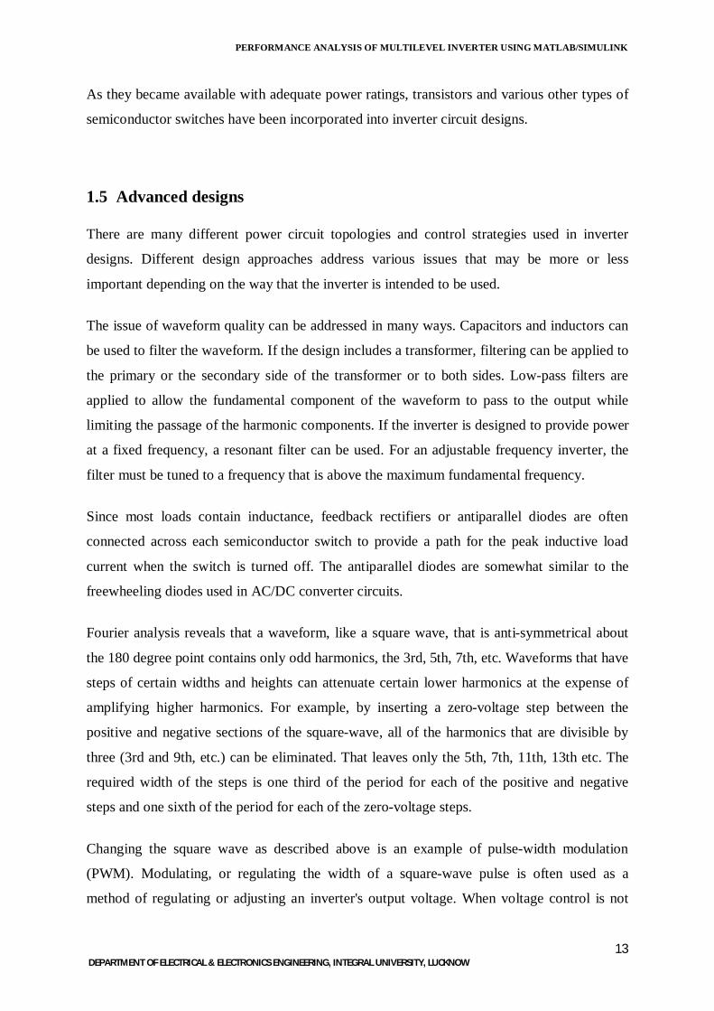
As they became available with adequate power ratings, transistors and various other types of
semiconductor switches have been incorporated into inverter circuit designs.
1.5 Advanced designs
There are many different power circuit topologies and control strategies used in inverter
designs. Different design approaches address various issues that may be more or less
important depending on the way that the inverter is intended to be used.
The issue of waveform quality can be addressed in many ways. Capacitors and inductors can
be used to filter the waveform. If the design includes a transformer, filtering can be applied to
the primary or the secondary side of the transformer or to both sides. Low-pass filters are
applied to allow the fundamental component of the waveform to pass to the output while
limiting the passage of the harmonic components. If the inverter is designed to provide power
at a fixed frequency, a resonant filter can be used. For an adjustable frequency inverter, the
filter must be tuned to a frequency that is above the maximum fundamental frequency.
Since most loads contain inductance, feedback rectifiers or antiparallel diodes are often
connected across each semiconductor switch to provide a path for the peak inductive load
current when the switch is turned off. The antiparallel diodes are somewhat similar to the
freewheeling diodes used in AC/DC converter circuits.
Fourier analysis reveals that a waveform, like a square wave, that is anti-symmetrical about
the 180 degree point contains only odd harmonics, the 3rd, 5th, 7th, etc. Waveforms that have
steps of certain widths and heights can attenuate certain lower harmonics at the expense of
amplifying higher harmonics. For example, by inserting a zero-voltage step between the
positive and negative sections of the square-wave, all of the harmonics that are divisible by
three (3rd and 9th, etc.) can be eliminated. That leaves only the 5th, 7th, 11th, 13th etc. The
required width of the steps is one third of the period for each of the positive and negative
steps and one sixth of the period for each of the zero-voltage steps.
Changing the square wave as described above is an example of pulse-width modulation
(PWM). Modulating, or regulating the width of a square-wave pulse is often used as a
method of regulating or adjusting an inverter's output voltage. When voltage control is not

PERFORMANCE ANALYSIS OF MULTILEVEL INVERTER USING MATLAB/SIMULINK
14 DEPARTMENT OF ELECTRICAL & ELECTRONICS ENGINEERING, INTEGRAL UNIVERSITY, LUCKNOW
required, a fixed pulse width can be selected to reduce or eliminate selected harmonics.
Harmonic elimination techniques are generally applied to the lowest harmonics because
filtering is much more practical at high frequencies, where the filter components can be much
smaller and less expensive. Multiple pulse-width or carrier based PWM control schemes
produce waveforms that are composed of many narrow pulses. The frequency represented by
the number of narrow pulses per second is called the switching frequency or carrier
frequency. These control schemes are often used in variable-frequency motor control
inverters because they allow a wide range of output voltage and frequency adjustment while
also improving the quality of the waveform.
Multilevel inverters provide another approach to harmonic cancellation. Multilevel inverters
provide an output waveform that exhibits multiple steps at several voltage levels. For
example, it is possible to produce a more sinusoidal wave by having split-rail direct current
inputs at two voltages, or positive and negative inputs with a central ground. By connecting
the inverter output terminals in sequence between the positive rail and ground, the positive
rail and the negative rail, the ground rail and the negative rail, then both to the ground rail, a
stepped waveform is generated at the inverter output. This is an example of a three level
inverter: the two voltages and ground.
1.6 Working
An inverter takes the DC input and runs it into a pair (or more) of power switching transistors. By
rapidly turning these transistors on and off, and feeding opposite sides of a transformer, it makes the
transformer think it is getting AC. The transformer changes this "alternating DC" into AC at the
output. Depending on the quality and complexity of the inverter, it may put out a square wave, a
"quasi-sine" (sometimes called modified sine) wave, or a true sine wave.
Quasi-sine (modified sine, modified square) wave inverters have more circuitry beyond the simple
switching, and put out a wave that looks like a stepped square wave - it is suitable for most standard
appliances, but may not work well with some electronics appliances that electronic heat or speed
control, or uses the AC for clocks or a timer.
Also, some of the chargers used for battery operated tools may not shut off when the battery is
charged, and should not be used with anything but sine wave inverters unless you are sure they will
work. Sine wave inverters put out a wave that is the same as you get from the power company - in
fact, it is often better and cleaner. Sine wave inverters can run anything, but are also more expensive
PERFORMANCE ANALYSIS OF MULTILEVEL INVERTER USING MATLAB/SIMULINK
15 DEPARTMENT OF ELECTRICAL & ELECTRONICS ENGINEERING, INTEGRAL UNIVERSITY, LUCKNOW
than other types. The quality of the "modified sine" (actually modified square wave), Quasi-sine
wave, etc. can also vary quite a bit between inverters, and may also vary somewhat with the load. The
very bottom end put out a wave that is nothing but a square wave, and is too "dirty" for all but
universal motor driven tools, coffee makers, toasters, and other appliances that have only a heating
element.
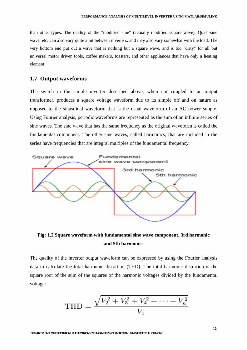
1.7 Output waveforms
The switch in the simple inverter described above, when not coupled to an output
transformer, produces a square voltage waveform due to its simple off and on nature as
opposed to the sinusoidal waveform that is the usual waveform of an AC power supply.
Using Fourier analysis, periodic waveforms are represented as the sum of an infinite series of
sine waves. The sine wave that has the same frequency as the original waveform is called the
fundamental component. The other sine waves, called harmonics, that are included in the
series have frequencies that are integral multiples of the fundamental frequency.
Fig: 1.2 Square waveform with fundamental sine wave component, 3rd harmonic
and 5th harmonics
The quality of the inverter output waveform can be expressed by using the Fourier analysis
data to calculate the total harmonic distortion (THD). The total harmonic distortion is the
square root of the sum of the squares of the harmonic voltages divided by the fundamental
voltage:

PERFORMANCE ANALYSIS OF MULTILEVEL INVERTER USING MATLAB/SIMULINK
16 DEPARTMENT OF ELECTRICAL & ELECTRONICS ENGINEERING, INTEGRAL UNIVERSITY, LUCKNOW
The quality of output waveform that is needed from an inverter depends on the characteristics
of the connected load. Some loads need a nearly perfect sine wave voltage supply in order to
work properly. Other loads may work quite well with a square wave voltage.

PERFORMANCE ANALYSIS OF MULTILEVEL INVERTER USING MATLAB/SIMULINK
17 DEPARTMENT OF ELECTRICAL & ELECTRONICS ENGINEERING, INTEGRAL UNIVERSITY, LUCKNOW
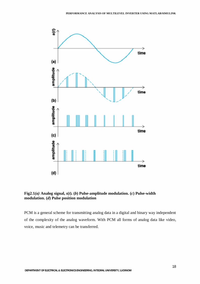
PULSE MODULATION SCHEME 2.1 Pulse Amplitude Modulation Pulse Amplitude Modulation refers to a method of carrying information on a train of pulses,
the information being encoded in the amplitude of pulses. In other words the pulse amplitude
is modulated according to the varying amplitude of analog signal.
2.2 Pulse Width Modulation Pulse Width Modulation refers to a method of carrying information on a train of pulses, the
information being encoded in the width of the pulses. The pulses have constant amplitude but
their duration varies in direct proportion to the amplitude of analog signal.
2.3 Pulse Position Modulation The amplitude and width of the pulse is kept constant in the system. The position of each
pulse, in relation to the position of a recurrent reference pulse, is varied by each instantaneous
sampled value of the modulating wave. PPM has the advantage of requiring constant
transmitter power since the pulses are of constant amplitude and duration.
2.4 Pulse Code Modulation To obtain PCM from an analog waveform at the source (transmitter), the analog signal
amplitude is sampled at regular time intervals. The sampling rate (number of samples per
second), is several times the maximum frequency of the analog waveform. The amplitude of
the analog signal at each sample is rounded off to the nearest binary level (quantization). The
Number of levels is always a power of 2 (4, 8, 16, 32, 64, ...). These numbers can be
represented by two, three, four, five, six or more binary digits.
PERFORMANCE ANALYSIS OF MULTILEVEL INVERTER USING MATLAB/SIMULINK
18 DEPARTMENT OF ELECTRICAL & ELECTRONICS ENGINEERING, INTEGRAL UNIVERSITY, LUCKNOW
Fig2.1(a) Analog signal, s(t). (b) Pulse-amplitude modulation. (c) Pulse-width modulation. (d) Pulse position modulation
PCM is a general scheme for transmitting analog data in a digital and binary way independent
of the complexity of the analog waveform. With PCM all forms of analog data like video,
voice, music and telemetry can be transferred.

PERFORMANCE ANALYSIS OF MULTILEVEL INVERTER USING MATLAB/SIMULINK
19 DEPARTMENT OF ELECTRICAL & ELECTRONICS ENGINEERING, INTEGRAL UNIVERSITY, LUCKNOW
2.5 Advantages of PWM
The output voltage control is easier with PWM than other schemes and can be
achieved without any additional components.
The lower order harmonics are either minimized or eliminated altogether.
The filtering requirements are minimized as lower order harmonics are eliminated and
higher order harmonics are filtered easily.
It has very low power consumption.
The entire control circuit can be digitized which reduces the susceptibility of the
circuit to interference.
Fig: 2.2 sine modulated, unmodulated signal
PWM is the most popular method for producing a controlled output for inverters. They are
quite popular in industrial applications.

PERFORMANCE ANALYSIS OF MULTILEVEL INVERTER USING MATLAB/SIMULINK
20 DEPARTMENT OF ELECTRICAL & ELECTRONICS ENGINEERING, INTEGRAL UNIVERSITY, LUCKNOW
2.6 Single Phase PWM Inverters
In many industrial applications, to control the output voltage of the inverters is necessary for
the following reasons
To adjust with variations of dc input voltage
To regulate voltage of inverters
To satisfy the contain volts and frequency control requirement
There are various techniques to vary the inverter gain. The most efficient method of
Controlling the gain (and output voltage) is to incorporate pulse width modulation (PWM)
Control within the inverters. The commonly used techniques are
a) Single Pulse width Modulation
b) Multiple Pulse width Modulation
c) Sinusoidal Pulse width Modulation
d) Modified sinusoidal Pulse width Modulation
e) Phase-displacement control.
The PWM techniques given above vary with respect to the harmonic content in their output
voltages.
2.7 Single Pulse Width Modulation In this control, there’s only one pulse per half cycle and the width of the pulse is varied to
control the inverter output. The gating signals are generated by comparing a rectangular
reference signal of the amplitude Ar with triangular carrier wave of amplitude Ac, the
frequency of the carrier wave determines the fundamental frequency of output voltage. By
varying Ar from 0 to Ac ,the pulse width can be varied from 0 to 100 percent. The ratio of Ar
to Ac is the control variable and defined as the modulation index.

PERFORMANCE ANALYSIS OF MULTILEVEL INVERTER USING MATLAB/SIMULINK
21 DEPARTMENT OF ELECTRICAL & ELECTRONICS ENGINEERING, INTEGRAL UNIVERSITY, LUCKNOW
2.8Multiple Pulse Width Modulation The harmonic content can be reduced by using several pulses in each half cycle of output
voltage. The generation of gating signals for turning ON and OFF transistors by comparing a
reference signal with a triangular carrier wave. The frequency Fc, determines the number of
pulses per half cycle. The modulation index controls the output voltage. This type of
modulation is also known as uniform pulse width modulation (UPWM).
2.9 Sinusoidal Pulse Width Modulation Modulation the width of each pulse is varied in proportion to the amplitude of a sine wave
evaluated at the centre of the same pulse. The distortion factor and lower order harmonics are
reduced significantly. The gating signals are generated by comparing a sinusoidal reference
signal with a Instead of, maintaining the width of all pulses of same as in case of multiple
pulse width triangular carrier wave of frequency Fc. The frequency of reference signal Fr
,determines the inverter output frequency and its peak amplitude Ar, controls the modulation
index M, and rms output voltage Vo. The number of pulses per half cycle depends on carrier
frequency.
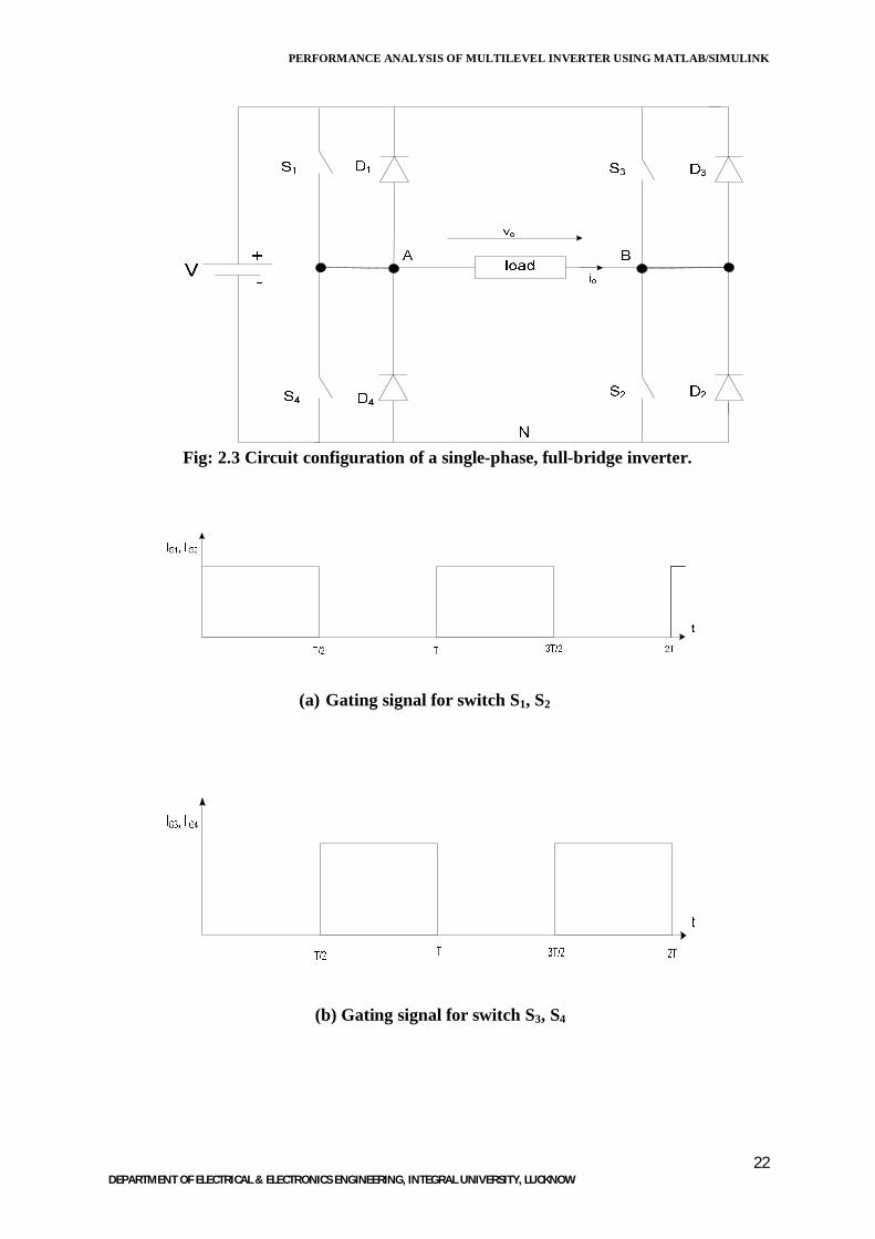
2.10 Single-phase, full-bridge, voltage-source inverters
The single-phase, half-bridge inverters require only two controlled switches and two diodes.
These inverters can be used only when three-wired dc supply is available. Moreover, the
voltage across the off-state semiconductor device is V, which is double the load voltage.
These drawbacks are removed in full bridge inverters (fig. 2.1). The inverter uses two pairs of
controlled switches (S1S2 and S3S4) and two pairs of diodes (D1D2 and D3D4). The devices of
one pair operate simultaneously. The gating signals of the switch-pairs S1S2 and S3S4 are
shown in Figs. 2.3 a & b, respectively.
PERFORMANCE ANALYSIS OF MULTILEVEL INVERTER USING MATLAB/SIMULINK
22 DEPARTMENT OF ELECTRICAL & ELECTRONICS ENGINEERING, INTEGRAL UNIVERSITY, LUCKNOW
Fig: 2.3 Circuit configuration of a single-phase, full-bridge inverter.
(a) Gating signal for switch S1, S2
(b) Gating signal for switch S3, S4
PERFORMANCE ANALYSIS OF MULTILEVEL INVERTER USING MATLAB/SIMULINK
23 DEPARTMENT OF ELECTRICAL & ELECTRONICS ENGINEERING, INTEGRAL UNIVERSITY, LUCKNOW
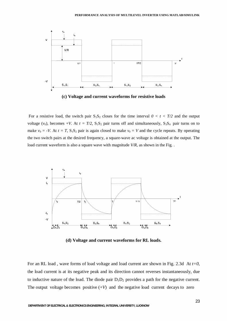
(c) Voltage and current waveforms for resistive loads
For a resistive load, the switch pair S1S2 closes for the time interval 0 < t < T/2 and the output
voltage (v0), becomes +V. At t = T/2, S1S2 pair turns off and simultaneously, S3S4 pair turns on to
make v0 = -V. At t = T, S1S2 pair is again closed to make v0 = V and the cycle repeats. By operating
the two switch pairs at the desired frequency, a square-wave ac voltage is obtained at the output. The
load current waveform is also a square wave with magnitude V/R, as shown in the Fig. .
(d) Voltage and current waveforms for RL loads.
For an RL load , wave forms of load voltage and load current are shown in Fig. 2.3d At t=0,
the load current is at its negative peak and its direction cannot reverses instantaneously, due
to inductive nature of the load. The diode pair D1D2 provides a path for the negative current.
The output voltage becomes positive (+V) and the negative load current decays to zero

PERFORMANCE ANALYSIS OF MULTILEVEL INVERTER USING MATLAB/SIMULINK
24 DEPARTMENT OF ELECTRICAL & ELECTRONICS ENGINEERING, INTEGRAL UNIVERSITY, LUCKNOW
at t = t1. During this period, energy is fed back to the source through the feedback diodes D1
and D2. At t = t1 , the diode pair D1D2 commutates and the switch pair S1S2, which is already
received the gating signal, turns on. It provides the path for the positive load current. The
load current builds up and reaches its positive peak at t = T/2. At this instant, the switch pair
S1S2 turns off. The positive current continues to flow for some more time (up to t=t2) through
the diode pair D3D4. As the load voltage is negative, the energy is fed back to the source. At t
= t2, D3D4 pair commutates and S3S4 pair starts conduction for the negative load current.
2.11 Unipolar switching scheme
In unipolar switching scheme, the switch pairs S1S2 and S3S4 of the full-bridge inverter of fig.
2.1, are not operated as pair. Instead, the switches of the first leg, i.e. S1 and S4, are operated
by comparing the triangular carrier wave (vc) with the sinusoidal reference signal (vref). The
switches of the other leg, i.e. S2 and S3, are operated by comparing vc with –vref. Following
logic is used to operate these switches:
1. If vref > vc, S1 is on and if vref < vc, S4 is on.
2. If –vref > vc, S3 is on and if –vref < vc, S2 is on.
Here Van and Vbn , are the potentials of the load terminals A and B, with respect to the
reference point N. The waveform for the unipolar switching scheme, mf =12 and ma= 0.8, are
shown in fig. 2.4. It may be observed that the output voltage fluctuates from 0 to +V in the
positive half-cycle and from 0 to –V in the negative half-cycle. Thus the scheme is called
unipolar switching scheme
Fig 2.4: Waveforms for unipolar voltage switching scheme
PERFORMANCE ANALYSIS OF MULTILEVEL INVERTER USING MATLAB/SIMULINK
25 DEPARTMENT OF ELECTRICAL & ELECTRONICS ENGINEERING, INTEGRAL UNIVERSITY, LUCKNOW
2.12 Performance parameters of inverters
Ideally, an inverter should give a sinusoidal voltage at its output. However, outputs of
practical inverters are non-sinusoidal and may be resolved into fundamental and harmonic
components. Performance of an inverter is usually assessed with the following performance
parameters.
2.12.1 Harmonic factor of nth harmonic
A harmonic factor is a measure of the individual harmonic contribution in the output voltage
of an inverter. It is defined as:
1VVHF n
n
Where Vn is the rms value of the nth harmonic component and v1 is the rms value of the
fundamental component of the output voltage.
2.12.2 Total harmonic distortion (THD)
A total harmonic distortion is a measure of closeness in a shape between the output voltage
waveform and its fundamental component. It is defined as the ratio of the rms value of the
total harmonic component of the output voltage and the rms value of the fundamental
component. Mathematically,
1
21
2
1
...3,2
2
VVV
V
VTHD rmsn
n
Where Vrms is the rms value of the output voltage.
PERFORMANCE ANALYSIS OF MULTILEVEL INVERTER USING MATLAB/SIMULINK
26 DEPARTMENT OF ELECTRICAL & ELECTRONICS ENGINEERING, INTEGRAL UNIVERSITY, LUCKNOW
2.12.3 Distortion factor (DF)
A distortion factor indicates the amount of harmonic that remain in the output voltage
waveform, after the waveform has been subjected to second order attenuation (i.e. divided by
n2).
1
...3,2
22 )/(
V
nVDF n
n
2.12.4 Lowest-order harmonics (LOH)
The lowest harmonic frequency, with a magnitude greater than or equal to three percent of
the magnitude of the fundamental component of the output voltage, is called the lowest order
harmonic. Higher the frequency of the LOH, lower will be the distortion in the current
waveform.

PERFORMANCE ANALYSIS OF MULTILEVEL INVERTER USING MATLAB/SIMULINK
27 DEPARTMENT OF ELECTRICAL & ELECTRONICS ENGINEERING, INTEGRAL UNIVERSITY, LUCKNOW
CIRCUIT DESCRIPTION
3.1 The IGBT (Insulated Gate Bipolar Transistor)
Fig:3.1 Circuit symbol of an IGBT (a)Circuit symbol (b) Photograph
The insulated gate bipolar transistor or IGBT is a voltage controlled four-layer, three-terminal
power semiconductor device, noted for high efficiency and fast switching. It is designed to
rapidly turn on and off, amplifiers that use it often synthesize complex waveforms with pulse
width modulation and low-pass filters. The IGBT combines the simple gate-drive
characteristics of the MOSFETs with the high-current and low–saturation-voltage capability
of bipolar transistors by combining an isolated gate FET for the control input, and a bipolar
power transistor as a switch, in a single device. The IGBT is used in medium-to- high power
applications.
Fig:3.2 Equivalent Circuit for IGBT
IGBTs can be classified as punch-through (PT) and non-punch-through (NPT) structures. In
the punch-through IGBT, a better trade-off between the forward voltage drop and turn-off
time can be achieved. Punch-through IGBTs are available up to about 1200 V. NPT IGBTs of
PERFORMANCE ANALYSIS OF MULTILEVEL INVERTER USING MATLAB/SIMULINK
28 DEPARTMENT OF ELECTRICAL & ELECTRONICS ENGINEERING, INTEGRAL UNIVERSITY, LUCKNOW
up to about 4 KV have been reported in literature and they are more robust than PT IGBTs
particularly under short circuit conditions. However they have a higher forward voltage drop
than the PT IGBTs. Its switching times can be controlled by suitably shaping the drive signal.
This gives the IGBT a number of advantages: it does not require protective circuits, it can be
connected in parallel without difficulty, and series connection is possible without dv/dt
snubbers. The IGBT is presently one of the most popular device in view of its wide ratings,
switching speed of about 100 KHz a easy voltage drive and a square Safe Operating Area
devoid of a Second Breakdown region.
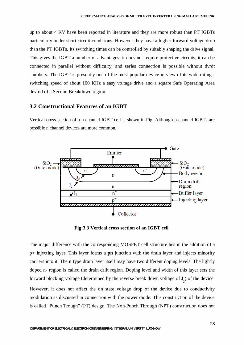
3.2 Constructional Features of an IGBT Vertical cross section of a n channel IGBT cell is shown in Fig. Although p channel IGBTs are
possible n channel devices are more common.
Fig:3.3 Vertical cross section of an IGBT cell.
The major difference with the corresponding MOSFET cell structure lies in the addition of a
p+ injecting layer. This layer forms a pn junction with the drain layer and injects minority
carriers into it. The n type drain layer itself may have two different doping levels. The lightly
doped n- region is called the drain drift region. Doping level and width of this layer sets the
forward blocking voltage (determined by the reverse break down voltage of J2) of the device.
However, it does not affect the on state voltage drop of the device due to conductivity
modulation as discussed in connection with the power diode. This construction of the device
is called “Punch Trough” (PT) design. The Non-Punch Through (NPT) construction does not

PERFORMANCE ANALYSIS OF MULTILEVEL INVERTER USING MATLAB/SIMULINK
29 DEPARTMENT OF ELECTRICAL & ELECTRONICS ENGINEERING, INTEGRAL UNIVERSITY, LUCKNOW
have this added n+ buffer layer. The PT construction does offer lower on state voltage drop
compared to the NPT construction particularly for lower voltage rated devices. However, it
does so at the cost of lower reverse break down voltage for the device, since the reverse break
down voltage of the junction J1is small. The rest of the construction of the device is very
similar to that of a vertical MOSFET including the insulated gate structure and the shorted
body (p type) – emitter (n+ type) structure. The doping level and physical geometry of the p
type body region however, is considerably different from that of a MOSFET in order to
defeat the latch up action of a parasitic thyristor embedded in the IGBT structure. A large
number of basic cells as shown in Fig 3.4 are grown on a single silicon wafer and connected
in parallel to form a complete IGBT device.
3.3 Operating principle of an IGBT
Fig:3.4 Parasitic thyristor in an IGBT cell (a)Schematic structure (b)Exact equivalent circuit (c)Approximate equivalent circuit
PERFORMANCE ANALYSIS OF MULTILEVEL INVERTER USING MATLAB/SIMULINK
30 DEPARTMENT OF ELECTRICAL & ELECTRONICS ENGINEERING, INTEGRAL UNIVERSITY, LUCKNOW
Operating principle of an IGBT can be explained in terms of the schematic cell structure and
equivalent circuit of Fig 3.4(a) and (c). From the input side the IGBT behaves essentially as a
MOSFET. Therefore, when the gate emitter voltage is less then the threshold voltage no
inversion layer is formed in the p type body region and the device is in the off state. The
forward voltage applied between the collector and the emitter drops almost entirely across the
junction J2. Very small leakage current flows through the device under this condition. In
terms of the equivalent current of Fig 3.4(c), when the gate emitter voltage is lower than the
threshold voltage the driving MOSFET of the Darlington configuration remains off and hence
the output p-n-p transistor also remains off.
When the gate emitter voltage exceeds the threshold, an inversion layer forms in the p type
body region under the gate. This inversion layer (channel) shorts the emitter and the drain
drift layer and an electron current flows from the emitter through this channel to the drain
drift region. This in turn causes substantial hole injection from the p+ type collector to the
drain drift region. A portion of these holes recombine with the electrons arriving at the drain
drift region through the channel. The rest of the holes cross the drift region to reach the p type
body where they are collected by the source metallization.
From the above discussion it is clear that the n type drain drift region acts as the base of the
output p-n-p transistor. The doping level and the thickness of this layer determines the current
gain “∝” of the p-n-p transistor. This is intentionally kept low so that most of the device current
flows through the MOSFET and not the output p-n-p transistor collector. This helps to reduced
the voltage drop across the “body” spreading resistance shown in Fig 3.4 (b) and eliminate the
possibility of static latch up of the IGBT.
The total on state voltage drop across a conducting IGBT has three components. The voltage drop
across J1
follows the usual exponential law of a pn junction. The next component of the voltage
drop is due to the drain drift region resistance. This component in an IGBT is considerably lower
compared to a MOSFET due to strong conductivity modulation by the injected minority carriers
from the collector. This is the main reason for reduced voltage drop across an IGBT compared to
an equivalent MOSFET. The last component of the voltage drop across an IGBT is due to the
channel resistance and its magnitude is equal to that of a comparable MOSFET.
PERFORMANCE ANALYSIS OF MULTILEVEL INVERTER USING MATLAB/SIMULINK
31 DEPARTMENT OF ELECTRICAL & ELECTRONICS ENGINEERING, INTEGRAL UNIVERSITY, LUCKNOW
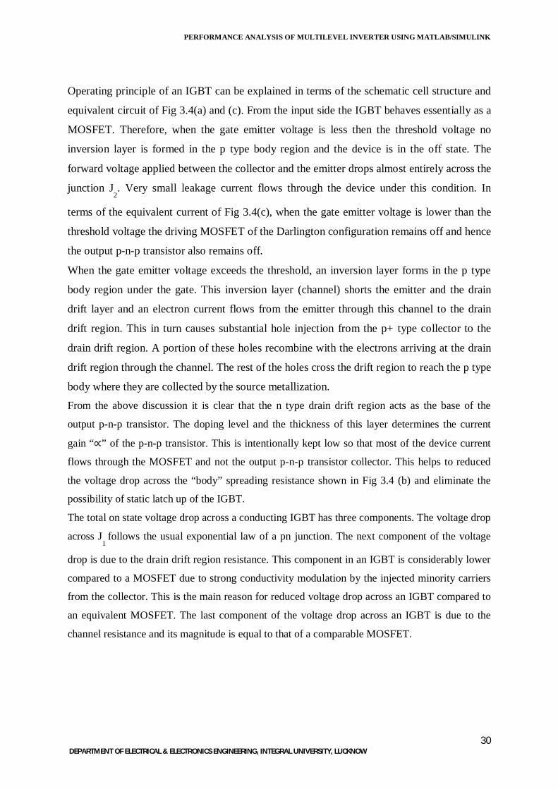
3.4 Switching characteristics of an IGBT Switching characteristics of the IGBT will be analyzed with respect to the clamped inductive
switching circuit shown in Fig 3.5(a). The equivalent circuit of the IGBT shown in Fig 3.5 (b)
will be used to explain the switching waveforms.
Fig.3.5: Inductive switching circuit using an IGBT
(a) Switching circuit (b) Equivalent circuit for the IGBT
The switching waveforms of an IGBT is in many respects similar to that of a Power
MOSFET. This is expected, since the input stage of an IGBT is a MOSFET as shown in Fig
3.5(b). Also in a modern IGBT a major portion of the total device current flows through the
MOSFET. Therefore, the switching voltage and current waveforms exhibit a strong similarity
with those of a MOSFET. However, the output p-n-p transistor does have a significant effect
on the switching characteristics of the device, particularly during turn off. Another important
difference is in the gate drive requirement. To avoid dynamic latch up, (to be discussed later)
the gate emitter voltage of an IGBT is maintained at a negative value when the device is off.
3.5 Parameters of an IGBT
Implement an IGBT device in parallel with a series RC snubber circuit. In ON state the IGBT
model has internal resistance (Ron) and inductance (Lon). In OF state the IGBT model has
infinite impedance. The internal inductance can not be set to zero.
The different parameter of an IGBT is used in simulation process are as follows
PERFORMANCE ANALYSIS OF MULTILEVEL INVERTER USING MATLAB/SIMULINK
32 DEPARTMENT OF ELECTRICAL & ELECTRONICS ENGINEERING, INTEGRAL UNIVERSITY, LUCKNOW
The different parameter of a diode used in simulation process are as follows
PERFORMANCE ANALYSIS OF MULTILEVEL INVERTER USING MATLAB/SIMULINK
33 DEPARTMENT OF ELECTRICAL & ELECTRONICS ENGINEERING, INTEGRAL UNIVERSITY, LUCKNOW
3.6 Comparison with Power MOSFETS
An IGBT has a significantly lower forward voltage drop compared to a conventional
MOSFET in higher blocking voltage rated devices. As the blocking voltage rating of both
MOSFET and IGBT devices increases, the depth of the n- drift region must increase and the
doping must decrease, resulting in roughly square relationship increase in forward conduction
loss compared to blocking voltage capability of the device. By injecting minority carriers
(holes) from the collector p+ region into the n- drift region during forward conduction, the
resistance of the n- drift region is considerably reduced. However, this resultant reduction in
on-state forward voltage comes with several penalties:
The additional PN junction blocks reverse current flow. This means that unlike a
MOSFET, IGBTs cannot conduct in the reverse direction. In bridge circuits where
reverse current flow is needed an additional diode (called a freewheeling diode) is
placed in parallel with the IGBT to conduct current in the opposite direction. The
penalty isn't as severe as first assumed though, because at the higher voltages where
IGBT usage dominates, discrete diodes are of significantly higher performance than
the body diode of a MOSFET.
The reverse bias rating of the N- drift region to collector P+ diode is usually only of
tens of volts, so if the circuit application applies a reverse voltage to the IGBT, an
additional series diode must be used.
The minority carriers injected into the n- drift region take time to enter and exit or
recombine at turn on and turn off. This results in longer switching time and hence
higher switching loss compared to a power MOSFET.
The on-state forward voltage drop in IGBTs behaves very differently to that in power
MOSFETS. The MOSFET voltage drop can be modeled as a resistance, with the
voltage drop proportional to current. By contrast, IGBT has a diode like voltage drop
(typically of the order of 2V) increasing only with the log of the current. Additionally,
MOSFET resistance is typically lower for smaller blocking voltages meaning that the
choice between IGBTs and power MOSFETS depend on both the blocking voltage
and current involved in a particular application, as well as the different switching
characteristics mentioned above. In general high voltage, high current and low switching
frequencies favor IGBTs while low voltage, low current and high switching frequencies are
the domain of the MOSFET.
PERFORMANCE ANALYSIS OF MULTILEVEL INVERTER USING MATLAB/SIMULINK
34 DEPARTMENT OF ELECTRICAL & ELECTRONICS ENGINEERING, INTEGRAL UNIVERSITY, LUCKNOW
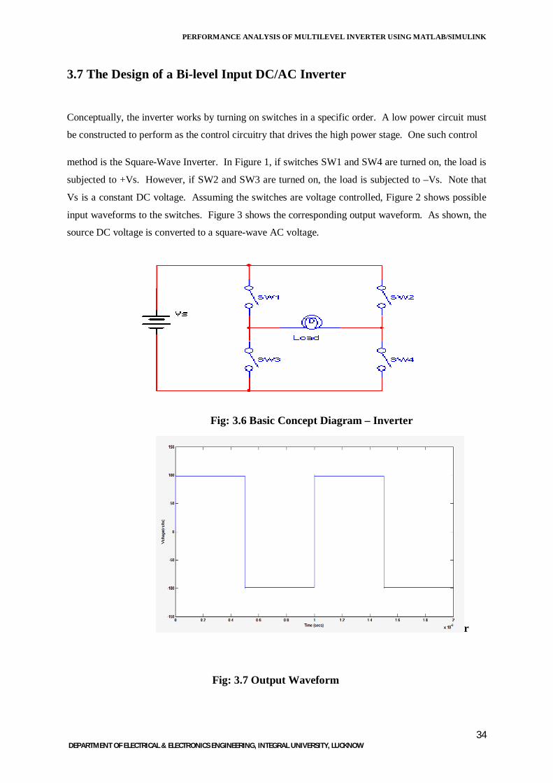
3.7 The Design of a Bi-level Input DC/AC Inverter
Conceptually, the inverter works by turning on switches in a specific order. A low power circuit must
be constructed to perform as the control circuitry that drives the high power stage. One such control
method is the Square-Wave Inverter. In Figure 1, if switches SW1 and SW4 are turned on, the load is
subjected to +Vs. However, if SW2 and SW3 are turned on, the load is subjected to –Vs. Note that
Vs is a constant DC voltage. Assuming the switches are voltage controlled, Figure 2 shows possible
input waveforms to the switches. Figure 3 shows the corresponding output waveform. As shown, the
source DC voltage is converted to a square-wave AC voltage.
Fig: 3.6 Basic Concept Diagram – Inverter
r
Fig: 3.7 Output Waveform
PERFORMANCE ANALYSIS OF MULTILEVEL INVERTER USING MATLAB/SIMULINK
35 DEPARTMENT OF ELECTRICAL & ELECTRONICS ENGINEERING, INTEGRAL UNIVERSITY, LUCKNOW
Since a square wave is not suitable for most applications, significant filtering must be
implemented to reduce the square wave to a sinusoidal wave. This can be accomplished
since a square wave can be represented as a Fourier series. The Fourier series of a square
wave is the sum of a sine wave of the fundamental frequency and its odd harmonics. Another
practical consideration is the fact that real switches can not change states
instantaneously. Therefore, there must be time when all switches are in the “off” state to
avoid shorting the supply voltage.
Another technique to control the output of an inverter is pulse-width modulation
(PWM). PWM control compares the output waveform to a reference signal and adjusts the
duty cycle of the switching mechanism. Compared to the square-wave method of control,
pulse-width modulation has two distinct advantages: higher frequency harmonic content and
amplitude control. The filtering requirements for PWM generated outputs are less stringent
since the non-fundamental components are of much higher frequency than that of the
fundamental sine wave. Also, by using PWM techniques, the output voltage of the inverter
can be directly controlled. Pulse-width modulators are available in IC packages and their
exact method of control varies by manufacturer and by model.
For PWM control, two inputs are required: a sinusoidal reference signal, also called a control
signal or a modulating signal, and a carrier signal. The triangle wave controls the switching
frequency of the inverter. Bipolar and unipolar switching are the two available methods of
switching. Both methods compare the reference signal and the carrier signal and cause
switching conditions that correspond to the two signals. For bipolar switching, the output is
either +VDC or –VDC corresponding to the reference voltage being greater than the carrier
wave and the reference being less than the carrier, respectively. The output is –VDC when the
sine wave is less than the carrier wave. For unipolar switching, the output is switched
between positive voltage and zero or negative voltage and zero.
PERFORMANCE ANALYSIS OF MULTILEVEL INVERTER USING MATLAB/SIMULINK
36 DEPARTMENT OF ELECTRICAL & ELECTRONICS ENGINEERING, INTEGRAL UNIVERSITY, LUCKNOW
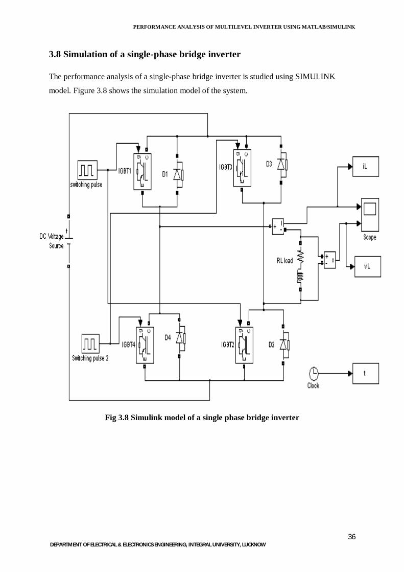
3.8 Simulation of a single-phase bridge inverter
The performance analysis of a single-phase bridge inverter is studied using SIMULINK
model. Figure 3.8 shows the simulation model of the system.
Fig 3.8 Simulink model of a single phase bridge inverter

PERFORMANCE ANALYSIS OF MULTILEVEL INVERTER USING MATLAB/SIMULINK
37 DEPARTMENT OF ELECTRICAL & ELECTRONICS ENGINEERING, INTEGRAL UNIVERSITY, LUCKNOW
There is a DC voltage source of 100 volt applied to a system. On and off period of the above
four switches (IGBT’s) are according to the gating signal below. Pulse generator is used for
switching.
Fig 3.9 (a)Gating signal for IGBT1 AND IGBT2
(b) Gating signal for IGBT3 AND IGBT4
For an RL load , wave forms of load current and load voltage are shown in Fig. (c) and (d)
simultaneously.
(c) Current waveform for RL loads (d) Voltage waveform for RL loads
PERFORMANCE ANALYSIS OF MULTILEVEL INVERTER USING MATLAB/SIMULINK
38 DEPARTMENT OF ELECTRICAL & ELECTRONICS ENGINEERING, INTEGRAL UNIVERSITY, LUCKNOW
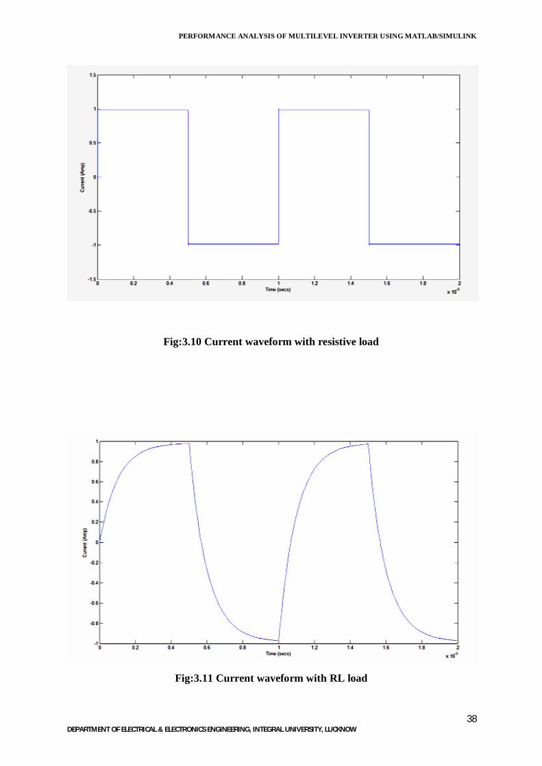
Fig:3.10 Current waveform with resistive load
Fig:3.11 Current waveform with RL load

PERFORMANCE ANALYSIS OF MULTILEVEL INVERTER USING MATLAB/SIMULINK
39 DEPARTMENT OF ELECTRICAL & ELECTRONICS ENGINEERING, INTEGRAL UNIVERSITY, LUCKNOW
Fig: 3.12 Voltage waveform with resistive load
At t=0, the load current is at its negative peak and its direction cannot reverses
instantaneously, due to inductive nature of the load. The diode pair D1D2 provides a path for
the negative current. The output voltage becomes positive (+V) and the negative load current
decays to zero at t = t1. During this period, energy is fed back to the source through the
feedback diodes D1 and D2. At t = t1 , the diode pair D1D2 commutates and the switch pair
S1S2, which is already received the gating signal, turns on. It provides the path for the
positive load current. The load current builds up and reaches its positive peak at t = T/2. At
this instant, the switch pair S1S2 turns off. The positive current continues to flow for some
more time (up to t=t2) through the diode pair D3D4. As the load voltage is negative, the
energy is fed back to the source. At t = t2, D3D4 pair commutates and S3S4 pair starts
conduction for the negative load current.
For a resistive load, the switch pair S1S2 closes for the time interval 0 < t < T/2 and the
output voltage (v0), becomes +V. At t = T/2, S1S2 pair turns off and simultaneously, S3S4 pair
turns on to make v0 = -V. At t = T, S1S2 pair is again closed to make v0 = V and the cycle
repeats. By operating the two switch pairs at the desired frequency, a square-wave ac voltage
is obtained at the output. The load current waveform is also a square wave with magnitude
V/R, as shown in the Fig.

PERFORMANCE ANALYSIS OF MULTILEVEL INVERTER USING MATLAB/SIMULINK
40 DEPARTMENT OF ELECTRICAL & ELECTRONICS ENGINEERING, INTEGRAL UNIVERSITY, LUCKNOW
3.9 Simulation of a single-phase bridge inverter using unipolar switching
In unipolar switching there is a comparison between the triangular carrier wave (vc) with the
sinusoidal reference signal (vref). The switches of the other leg, i.e. S2 and S3, are operated by
comparing vc with –vref. The SIMULINK model of unipolar switching for the inverter is
shown in figure 2.7, and various switching pulses for the four IGBT switches are shown in
figure 2.8
Fig: 3.13 Switching Block in inverter

PERFORMANCE ANALYSIS OF MULTILEVEL INVERTER USING MATLAB/SIMULINK
41 DEPARTMENT OF ELECTRICAL & ELECTRONICS ENGINEERING, INTEGRAL UNIVERSITY, LUCKNOW
Time (secs) Time (secs)
(a)Switching pulse for IGBT1 (b) Switching pulse for IGBT2
Time (secs) Time (secs)
(c) Switching pulse for IGBT3 (d) Switching pulse for IGBT4
Fig:3.14 Switching pulses for different switches of inverter
PERFORMANCE ANALYSIS OF MULTILEVEL INVERTER USING MATLAB/SIMULINK
42 DEPARTMENT OF ELECTRICAL & ELECTRONICS ENGINEERING, INTEGRAL UNIVERSITY, LUCKNOW
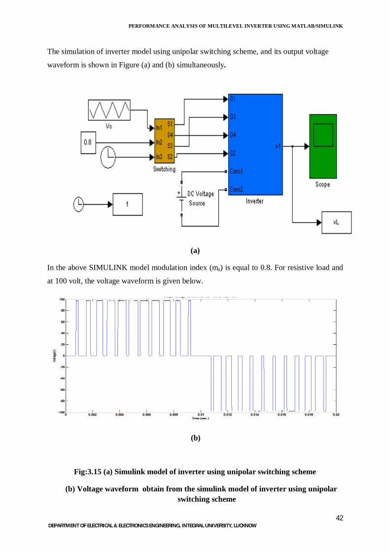
The simulation of inverter model using unipolar switching scheme, and its output voltage
waveform is shown in Figure (a) and (b) simultaneously.
(a)
In the above SIMULINK model modulation index (ma) is equal to 0.8. For resistive load and
at 100 volt, the voltage waveform is given below.
(b)
Fig:3.15 (a) Simulink model of inverter using unipolar switching scheme
(b) Voltage waveform obtain from the simulink model of inverter using unipolar switching scheme

PERFORMANCE ANALYSIS OF MULTILEVEL INVERTER USING MATLAB/SIMULINK
43 DEPARTMENT OF ELECTRICAL & ELECTRONICS ENGINEERING, INTEGRAL UNIVERSITY, LUCKNOW
ANALYSIS OF MULTILEVEL INVERTER
4.1 INTRODUCTION
MULTILEVEL topologies are able to generate better output quality, while operating at lower
switching frequency. This implies lower switching dissipation and higher efficiency.
Moreover, this topology utilizes switches with lower breakdown voltage; therefore, it can be
used in higher power applications at lower cost. It is worth mentioning that although the
number of switches in this approach is higher than other two level topologies, for a sufficient
high number of levels, the output filter can be avoided which means less weight, cost and
space. On the other hand, even with the same size of filter at the output, the switching
frequency can be decreased which means higher efficiency. In general, a greater number of
switches in multilevel converters can be justified since the semiconductor cost decreases at a
much greater rate than the filter components cost.
Numerous industrial applications have begun to require higher power apparatus in recent
years. Some medium voltage motor drives and utility applications require medium voltage
and megawatt power level. For a medium voltage grid, it is troublesome to connect only one
power semiconductor switch directly. As a result, a multilevel power converter structure has
been introduced as an alternative in high power and medium voltage situations. A multilevel
converter not only achieves high power ratings, but also enables the use of renewable energy
sources. Renewable energy sources such as photovoltaic, wind, and fuel cells can be easily
interfaced to a multilevel converter system for a high power application.
The concept of multilevel converters has been introduced since 1975. The term multilevel
began with the three-level converter. Subsequently, several multilevel converter topologies
have been developed. However, the elementary concept of a multilevel converter to achieve
higher power is to use a series of power semiconductor switches with several lower voltage
dc sources to perform the power conversion by synthesizing a staircase voltage waveform.
Capacitors, batteries, and renewable energy voltage sources can be used as the multiple dc
voltage sources. The commutation of the power switches aggregate these multiple dc sources
in order to achieve high voltage at the output; however, the rated voltage of the power
semiconductor switches depends only upon the rating of the dc voltage sources to which they
are connected.
PERFORMANCE ANALYSIS OF MULTILEVEL INVERTER USING MATLAB/SIMULINK
44 DEPARTMENT OF ELECTRICAL & ELECTRONICS ENGINEERING, INTEGRAL UNIVERSITY, LUCKNOW
In general, increasing the switching frequency in voltage source inverters (VSI) leads to the
better output voltage current waveforms. Harmonic reduction in controlling a VSI with
variable amplitude and frequency of the output voltage is of importance and thus the
conventional inverters which are referred to as two-level inverters have required increased
switching frequency along with various PWM switching strategies. In the case of high power
high voltage applications, however, the two-level inverters have some limitations to operate
at high frequency mainly due to switching losses and constraints of device rating itself.
Moreover, the semiconductor switching devices should be used in such a manner as
problematic serried parallel combinations to obtain capability of handling high power.
Nowadays the use of multilevel approach is believed to be promising alternative in such a
very high power conversion processing as pointed out in literatures.
A multilevel converter has several advantages over a conventional two-level converter that
uses high switching frequency pulse width modulation (PWM). The attractive features of a
multilevel converter can be briefly summarized as follows.
● Staircase waveform quality: Multilevel converters not only can generate the output voltages
with very low distortion, but also can reduce the dv/dt stresses; therefore electromagnetic
compatibility (EMC) problems can be reduced.
● Input current: Multilevel converters can draw input current with low distortion.
● Switching frequency: Multilevel converters can operate at both fundamental switching
frequency and high switching frequency PWM. It should be noted that lower switching
frequency usually means lower switching loss and higher efficiency.
Unfortunately, multilevel converters do have some disadvantages. One particular
disadvantage is the greater number of power semiconductor switches needed. Although lower
voltage rated switches can be utilized in a multilevel converter, each switch requires a related
gate drive circuit. This may cause the overall system to be more expensive and complex.
PERFORMANCE ANALYSIS OF MULTILEVEL INVERTER USING MATLAB/SIMULINK
45 DEPARTMENT OF ELECTRICAL & ELECTRONICS ENGINEERING, INTEGRAL UNIVERSITY, LUCKNOW
4.3 BASIC PRINCIPLE OF OPERATION OF CASCADED MULTILEVEL
INVERTER
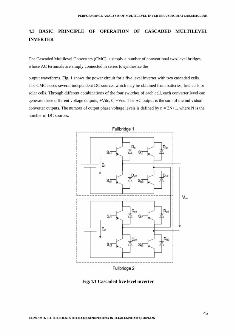
The Cascaded Multilevel Converters (CMC) is simply a number of conventional two-level bridges,
whose AC terminals are simply connected in series to synthesize the
output waveforms. Fig. 1 shows the power circuit for a five level inverter with two cascaded cells.
The CMC needs several independent DC sources which may be obtained from batteries, fuel cells or
solar cells. Through different combinations of the four switches of each cell, each converter level can
generate three different voltage outputs, +Vdc, 0, −Vdc. The AC output is the sum of the individual
converter outputs. The number of output phase voltage levels is defined by n = 2N+1, where N is the
number of DC sources.
Fig:4.1 Cascaded five level inverter
PERFORMANCE ANALYSIS OF MULTILEVEL INVERTER USING MATLAB/SIMULINK
46 DEPARTMENT OF ELECTRICAL & ELECTRONICS ENGINEERING, INTEGRAL UNIVERSITY, LUCKNOW
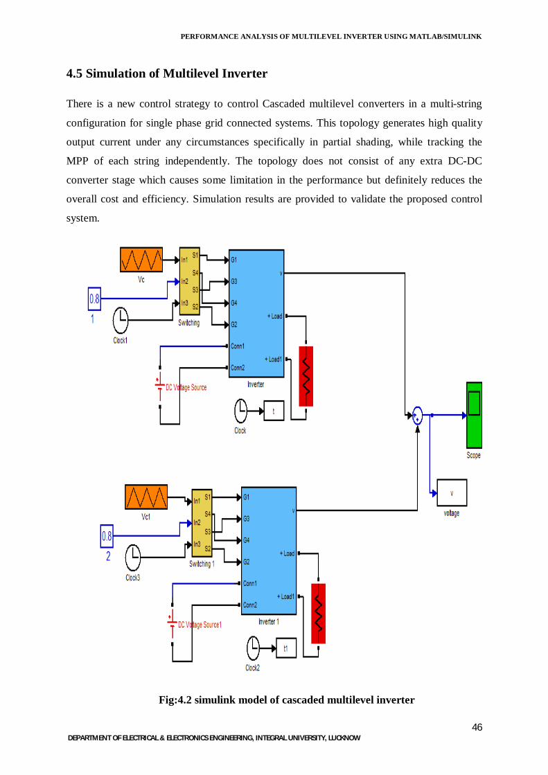
4.5 Simulation of Multilevel Inverter
There is a new control strategy to control Cascaded multilevel converters in a multi-string
configuration for single phase grid connected systems. This topology generates high quality
output current under any circumstances specifically in partial shading, while tracking the
MPP of each string independently. The topology does not consist of any extra DC-DC
converter stage which causes some limitation in the performance but definitely reduces the
overall cost and efficiency. Simulation results are provided to validate the proposed control
system.
Fig:4.2 simulink model of cascaded multilevel inverter
PERFORMANCE ANALYSIS OF MULTILEVEL INVERTER USING MATLAB/SIMULINK
47 DEPARTMENT OF ELECTRICAL & ELECTRONICS ENGINEERING, INTEGRAL UNIVERSITY, LUCKNOW
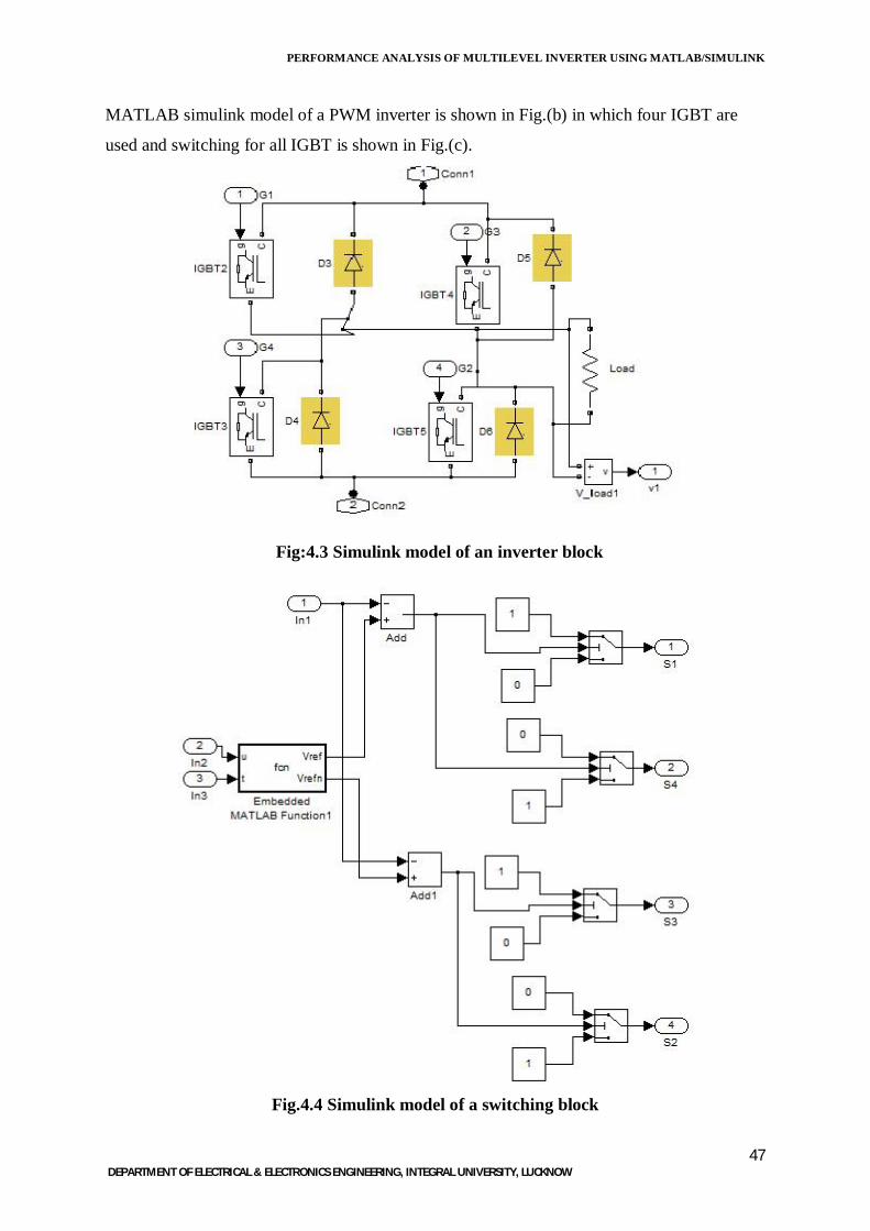
MATLAB simulink model of a PWM inverter is shown in Fig.(b) in which four IGBT are
used and switching for all IGBT is shown in Fig.(c).
Fig:4.3 Simulink model of an inverter block
Fig.4.4 Simulink model of a switching block

PERFORMANCE ANALYSIS OF MULTILEVEL INVERTER USING MATLAB/SIMULINK
48 DEPARTMENT OF ELECTRICAL & ELECTRONICS ENGINEERING, INTEGRAL UNIVERSITY, LUCKNOW
In unipolar switching scheme, the switch pairs S1S2 and S3S4 of the full-bridge inverter of fig.
2.1, are not operated as pair. Instead, the switches of the first leg, i.e. S1 and S4, are operated
by comparing the triangular carrier wave (vc) with the sinusoidal reference signal (vref). The
switches of the other leg, i.e. S2 and S3, are operated by comparing vc with –vref. Following
logic is used to operate these switches:
1. If vref > vc, S1 is on and if vref < vc, S4 is on.
2. If –vref > vc, S3 is on and if –vref < vc, S2 is on.
Fig:4.5 output voltage waveform at ma1=0.8 & ma2=0.8.
PERFORMANCE ANALYSIS OF MULTILEVEL INVERTER USING MATLAB/SIMULINK
49 DEPARTMENT OF ELECTRICAL & ELECTRONICS ENGINEERING, INTEGRAL UNIVERSITY, LUCKNOW
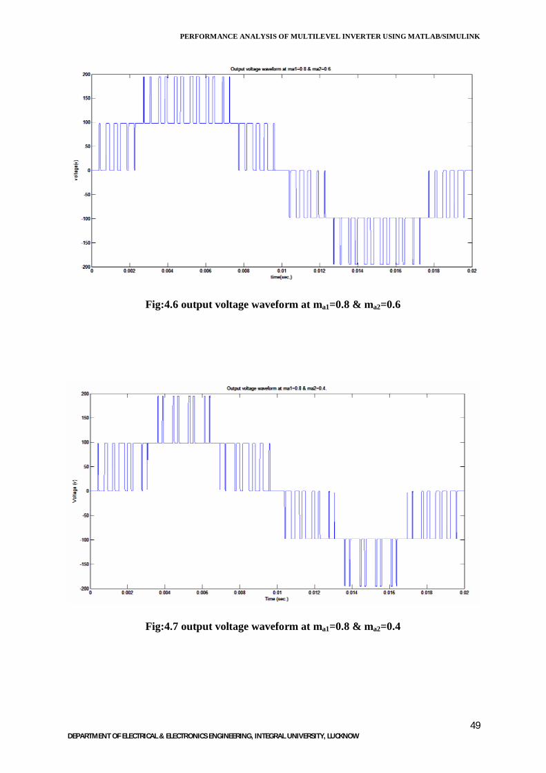
Fig:4.6 output voltage waveform at ma1=0.8 & ma2=0.6
Fig:4.7 output voltage waveform at ma1=0.8 & ma2=0.4

PERFORMANCE ANALYSIS OF MULTILEVEL INVERTER USING MATLAB/SIMULINK
50 DEPARTMENT OF ELECTRICAL & ELECTRONICS ENGINEERING, INTEGRAL UNIVERSITY, LUCKNOW
Through different combinations of the four switches of both cells, both converter levels can
generate three different voltage outputs, +Vdc, 0, −Vdc. The AC output is the sum of the
individual converter outputs. The number of output phase voltage levels is ‘5’ because we use
two photovoltaic sources. For instance the output range of the Fig. 4.5 swings from −200to
+200 with five levels.
In above figure output voltage waveform for various value of different modulation
index(ma)are shown. The pulse width of voltage waveform decreases by decreasing the value
of modulation index(ma2) and have constant modulation index (ma1)
4.6 Merits of Multilevel Inverter
Multilevel concept is used to decrease the harmonic distortion in the output waveform
without decreasing the inverter power output.
• To increase inverter operating voltage without devices in series.
• To minimize THD with low switching frequencies fsw.
• To reduce EMI due to lower voltage steps.
• Ability to reduce the voltage stress on each power device due to the utilization of
multiple levels on the DC bus.
• Important when a high DC side voltage is imposed by an application (e.g. traction
systems)
• Even at low switching frequencies, smaller distortion in the multilevel inverter AC
side waveform can be achieved (with stepped modulation technique)
• Reduced electromagnetic compatibility (EMC) when operated at high voltage.
• Smaller rating of semiconductor devices.
• Better feature in output voltage in terms of less distortion.
• Lower harmonic contents and lower switching loses.

PERFORMANCE ANALYSIS OF MULTILEVEL INVERTER USING MATLAB/SIMULINK
51 DEPARTMENT OF ELECTRICAL & ELECTRONICS ENGINEERING, INTEGRAL UNIVERSITY, LUCKNOW
• The circuit topology provides full utilization of semiconductor devices like GTOs
where voltage stress of each switch is limited to certain lower value than dc link
whereby increased handling power capability of the inverter.
• They are suitable for high voltage and high current application.
• They have higher efficiency because the devices can be switched at low frequency.
4.7 Demerits of Multilevel Inverter
The drawbacks are the isolated power supplies required for each one of the stages of
the multiconverter and it’s also lot harder to build, more expensive, harder to control
in software.
Switching utilization and efficiency are poor for real transmission.
The large number of capacitors are both more expensive and bulky than clamping
diodes in multilevel diode clamped converters. Packaging is also more difficult in
inverters with high number of levels.
PERFORMANCE ANALYSIS OF MULTILEVEL INVERTER USING MATLAB/SIMULINK
52 DEPARTMENT OF ELECTRICAL & ELECTRONICS ENGINEERING, INTEGRAL UNIVERSITY, LUCKNOW
HARMONICS ANALYSIS OF MULTILEVEL INVERTER
Harmonics are currents or voltages with frequencies that are integer multiples of the
fundamental power frequency being 50 or 60Hz (50Hz for European power and 60Hz for
American power). For example, if the fundamental power frequency is 50 Hz, then the
2nd harmonic is 100 Hz, the 3rd is 150 Hz, etc. In modern test equipment today harmonics can
be measured up to the 63rd harmonics.
To give an understanding of this, consider a water piping system. Have you ever taken a
shower when someone turns on the cold water at the sink? You experience the effect of a
pressure drop to the cold water, reducing the flow of cold water. The end result is you get
burned! Now imagine that someone at a sink alternately turns on and off the cold and hot
water. You would effectively be hit with alternating cold and hot water! Therefore, the
performance and function of the shower is reduced by other systems. This illustration is
similar to an electrical distribution system with non-linear loads generating harmonics.
There are several industrial applications which may allow a harmonic content of 5% of its
fundamental component of input voltage when inverters are used. Actually, the inverter
output voltage may have harmonic content much higher than 5% of its fundamental
component. In order to bring this harmonic content to a reasonable limit of 5%, one method is
to insert filters between the load and inverter. If the inverter output voltage contains high
frequency harmonics, these can be reduced by a low-size filter. For the attenuation of low-
frequency harmonics, however, the size of filter components increases. This makes the filter
circuit costly, bulky and weighty and in addition, the transient response of the system
becomes sluggish. This shows that lower order harmonics from the inverter output voltage
should be reduced by some means other the filter.

PERFORMANCE ANALYSIS OF MULTILEVEL INVERTER USING MATLAB/SIMULINK
53 DEPARTMENT OF ELECTRICAL & ELECTRONICS ENGINEERING, INTEGRAL UNIVERSITY, LUCKNOW
5.1 Harmonic Optimization Techniques in Multilevel VSI
One of the major problems in electric power quality is the harmonic contents. There are
several methods of indicating the quantity of harmonic contents. The most widely used
measure is the total harmonic distortion (THD). Various switching techniques have been used
in static converters to reduce the output harmonic content.
We compare the two harmonic optimization techniques, known as optimal minimization of
the total harmonic distortion (OMTHD) technique and optimized harmonic stepped-
waveform (OHSW) technique used in multi-level inverters with unequal dc sources. Both
techniques are very effective and efficient for improving the quality of the inverter output
voltage. First, we describe briefly the cascaded H-bridge multi-level inverter structure.
Multi-level inverter is recently used in many industrial applications such as ac power
supplies, static VAR compensators, drive systems, etc. One of the significant advantages of
multi-level structure is the harmonic reduction in the output waveform without increasing
switching frequency or decreasing the inverter output power. The output voltage waveform of
a multi-level inverter is composed of a number of levels of voltages, typically obtained from
capacitor voltage sources.
The so-called multi-level starts from three levels. As the number of levels increases, the
output THD approaches zero. The number of achievable voltage levels, however, is limited
by voltage unbalance problems, voltage clamping requirement, circuit layout, and packaging
constraints. Therefore, an important key in designing an effective and efficient multi-level
inverter is to ensure that the total harmonic distortion (THD) in the output voltage waveform
is small enough. The well-known multi-level inverter topologies are: cascaded H-bridge
multi-level inverter, diode-clamped multi-level inverter and flying capacitor multi-level
inverter. The multi-level inverter composed of cascaded H-bridges with separate dc sources
(SDCSs), hereafter called a cascaded multi-level inverter, appears to be superior to the other
multi-level topologies in terms of its structure that is not only simple and modular but also
requires the least number of components. This modular structure makes it easily extensible to
higher number of output voltage levels without undue increase in power circuit complexity.
In addition, extra clamping diodes or voltage balancing capacitors are not necessary. It is
generally accepted that the performance of an inverter, with any switching strategy, can be
related to the harmonic contents of its output voltage. Power electronics researchers have
always studied many novel control techniques to reduce harmonics in such waveforms.Up to
PERFORMANCE ANALYSIS OF MULTILEVEL INVERTER USING MATLAB/SIMULINK
54 DEPARTMENT OF ELECTRICAL & ELECTRONICS ENGINEERING, INTEGRAL UNIVERSITY, LUCKNOW
now, in multi-level technology, several well-known modulation techniques have been used as
follows: Harmonic Optimization, Space Vector PWM (SV-PWM), and Carrier-Based PWM
techniques.
The harmonic optimization techniques can be categorized into two methods: Optimal
Minimization of the Total Harmonic Distortion (OMTHD) and Optimized Harmonic
Stepped-Waveform (OHSW). OMTHD technique is based on minimization of THD by
reducing all harmonics with no emphasis on any particular component, where as, OHSW is
based on elimination of some specific harmonic components. In this paper, OMTHD and
OHSW techniques are applied to a cascaded multi-level inverter with non-equal dc sources.
Usually, it is assumed that the dc sources are all equal, which will not probably be the case in
practice even if the dc sources are nominally equal. Here the dc sources are taken with
different voltages for generality of the study. The study is performed for both cases focusing
on harmonic content of the output voltage and the results obtained by the two techniques are
compared. The paper is organized as follows: First the cascaded H-bridge multilevel
inverter’s structure and operation are briefly described. Then, the switching algorithms for the
multilevel inverter, based on OHSW and OMTHD techniques are explained. Finally, the
results obtained for the two techniques are analyzed and compared. Also, several informative
results verify the effectiveness of both techniques in multi-level inverter with non-equal dc
sources, clarifying the advantages of each technique.
PERFORMANCE ANALYSIS OF MULTILEVEL INVERTER USING MATLAB/SIMULINK
55 DEPARTMENT OF ELECTRICAL & ELECTRONICS ENGINEERING, INTEGRAL UNIVERSITY, LUCKNOW
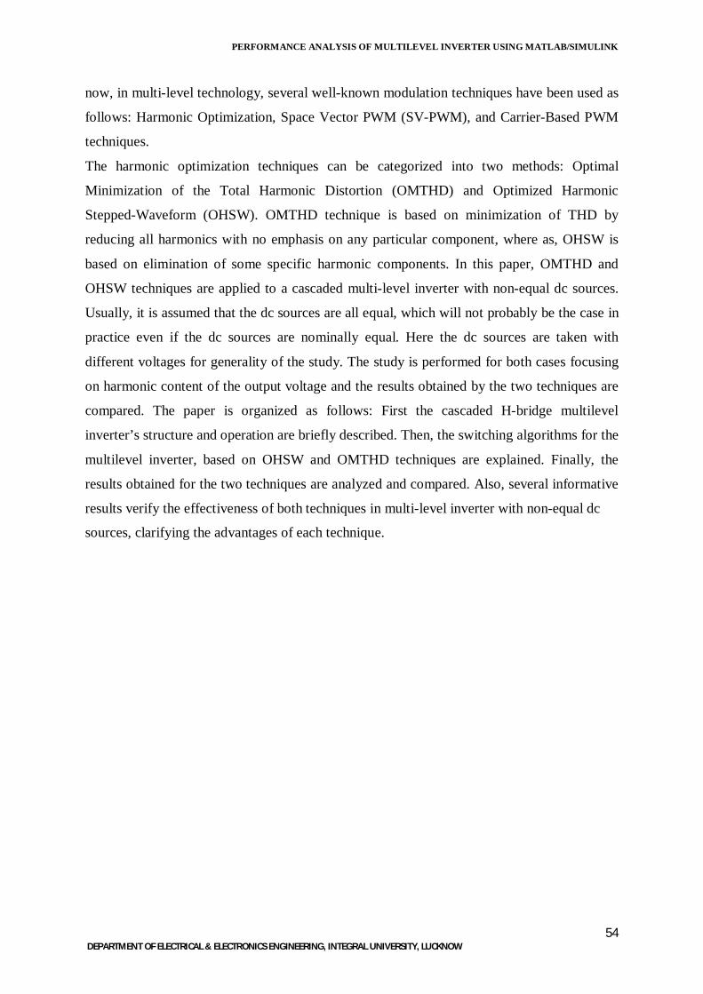
5.2 Harmonics evaluation of single & multilevel inverter
Harmonics Harmonic factor of single inverter when ma1=0.8,ma2=0.8
Harmonic factor of multilevel inverter when ma1=o.8 , ma2=0.8
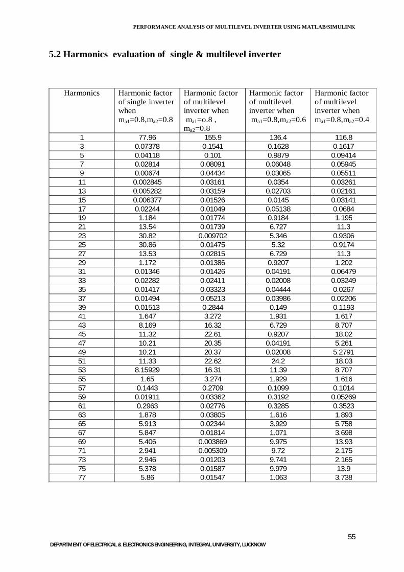
Harmonic factor of multilevel inverter when ma1=0.8,ma2=0.6
Harmonic factor of multilevel inverter when ma1=0.8,ma2=0.4
1 77.96 155.9 136.4 116.8 3 0.07378 0.1541 0.1628 0.1617 5 0.04118 0.101 0.9879 0.09414 7 0.02814 0.08091 0.06048 0.05945 9 0.00674 0.04434 0.03065 0.05511
11 0.002845 0.03161 0.0354 0.03261 13 0.005282 0.03159 0.02703 0.02161 15 0.006377 0.01526 0.0145 0.03141 17 0.02244 0.01049 0.05138 0.0684 19 1.184 0.01774 0.9184 1.195 21 13.54 0.01739 6.727 11.3 23 30.82 0.009702 5.346 0.9306 25 30.86 0.01475 5.32 0.9174 27 13.53 0.02815 6.729 11.3 29 1.172 0.01386 0.9207 1.202 31 0.01346 0.01426 0.04191 0.06479 33 0.02282 0.02411 0.02008 0.03249 35 0.01417 0.03323 0.04444 0.0267 37 0.01494 0.05213 0.03986 0.02206 39 0.01513 0.2844 0.149 0.1193 41 1.647 3.272 1.931 1.617 43 8.169 16.32 6.729 8.707 45 11.32 22.61 0.9207 18.02 47 10.21 20.35 0.04191 5.261 49 10.21 20.37 0.02008 5.2791 51 11.33 22.62 24.2 18.03 53 8.15929 16.31 11.39 8.707 55 1.65 3.274 1.929 1.616 57 0.1443 0.2709 0.1099 0.1014 59 0.01911 0.03362 0.3192 0.05269 61 0.2963 0.02776 0.3285 0.3523 63 1.878 0.03805 1.616 1.893 65 5.913 0.02344 3.929 5.758 67 5.847 0.01814 1.071 3.698 69 5.406 0.003869 9.975 13.93 71 2.941 0.005309 9.72 2.175 73 2.946 0.01203 9.741 2.165 75 5.378 0.01587 9.979 13.9 77 5.86 0.01547 1.063 3.738

PERFORMANCE ANALYSIS OF MULTILEVEL INVERTER USING MATLAB/SIMULINK
56 DEPARTMENT OF ELECTRICAL & ELECTRONICS ENGINEERING, INTEGRAL UNIVERSITY, LUCKNOW
Fig 5.1 Harmonic evaluation on single phase inverter
Fig 5.2 Harmonic evaluation of multilevel inverter when ma1=0.8 & ma2=0.8
0102030405060708090
1 3 5 7 9 1113151719212325272931333537394143454749515355575961636567697173757779
Har
mon
ic fa
ctor
(% o
f fun
dam
enta
l)
Harmonic number
Harmonic factor of single phase inverter when ma1=0.8 & ma2=0.8
0
20
40
60
80
100
120
140
160
180
1 3 5 7 9 1113151719212325272931333537394143454749515355575961636567697173757779
harm
onic
s fac
tor(
% o
f fun
dam
enta
l)
harmonic number
Harmonic factor of multilevel inverter
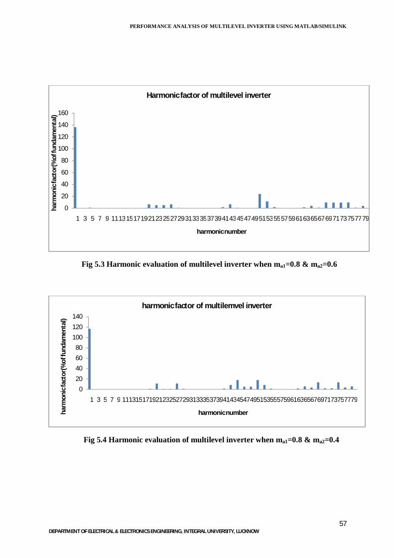
PERFORMANCE ANALYSIS OF MULTILEVEL INVERTER USING MATLAB/SIMULINK
57 DEPARTMENT OF ELECTRICAL & ELECTRONICS ENGINEERING, INTEGRAL UNIVERSITY, LUCKNOW
Fig 5.3 Harmonic evaluation of multilevel inverter when ma1=0.8 & ma2=0.6
Fig 5.4 Harmonic evaluation of multilevel inverter when ma1=0.8 & ma2=0.4
0
20
40
60
80
100
120
140
160
1 3 5 7 9 1113151719212325272931333537394143454749515355575961636567697173757779
harm
onic
fact
or(%
of fu
ndam
enta
l)
harmonic number
Harmonic factor of multilevel inverter
020406080
100120140
1 3 5 7 9 1113151719212325272931333537394143454749515355575961636567697173757779
harm
onic
fact
or(%
of fu
ndam
enta
l)
harmonic number
harmonic factor of multilemvel inverter

PERFORMANCE ANALYSIS OF MULTILEVEL INVERTER USING MATLAB/SIMULINK
58 DEPARTMENT OF ELECTRICAL & ELECTRONICS ENGINEERING, INTEGRAL UNIVERSITY, LUCKNOW
5.3 Applications in Harmonic Elimination
The present chapter helps us to understand the effects of non-linear loads on the power
system and the implementation of suitable devices to cancel out the harmonics. The use of
inverters in active power filters has been emphasized and the simulated circuits and results
have been described in particular.
5.3.1 Non Linear Loads A non-linear load on a power system is typically a rectifier or some kind of arc discharge
device such as a fluorescent lamp, electric welding machine, or arc furnace in which current
is not linearly related to the voltage. Because current in these systems is interrupted by a
switching action, the current contains frequency components that are multiples of the power
system frequency. This leads to distortion of the current waveform which in turn distorts the
voltage waveform. Distortion power factor is a measure of how much the harmonic distortion
of a load current decreases the average power transferred to the load.
5.3.2 Active Power Filters
The increasing use of power electronics based loads (adjustable speed drives, switch mode
power supplies, etc.) to improve system efficiency and controllability is increasing the
concern for harmonic distortion levels in end use facilities and on the overall power system.
The application of passive tuned filters creates new system resonances which are dependent
on specific system conditions.
In general, passive tuned filters have been used to minimize low-frequency current harmonics
while high-pass units have been connected to attenuate the amplitude of high frequency
current components. However, high-pass filters present disadvantages due to the resistance
connected in parallel to the inductor, which increases the filter losses and reduces the filtering
effectiveness at the tuned frequency. The most critical aspects of passive filters are related to
the fact that they cannot modify their compensation characteristics following the dynamic
changes of the nonlinear load, the performance dependence they present with the power
system parameters, and the probability of series resonances with the power system’s
equivalent reactance. Passive filter ratings must be coordinated with reactive power
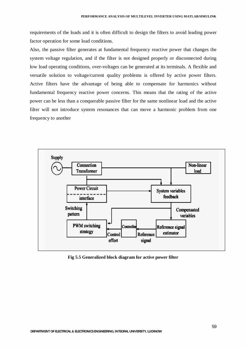
PERFORMANCE ANALYSIS OF MULTILEVEL INVERTER USING MATLAB/SIMULINK
59 DEPARTMENT OF ELECTRICAL & ELECTRONICS ENGINEERING, INTEGRAL UNIVERSITY, LUCKNOW
requirements of the loads and it is often difficult to design the filters to avoid leading power
factor operation for some load conditions.
Also, the passive filter generates at fundamental frequency reactive power that changes the
system voltage regulation, and if the filter is not designed properly or disconnected during
low load operating conditions, over-voltages can be generated at its terminals. A flexible and
versatile solution to voltage/current quality problems is offered by active power filters.
Active filters have the advantage of being able to compensate for harmonics without
fundamental frequency reactive power concerns. This means that the rating of the active
power can be less than a conquerable passive filter for the same nonlinear load and the active
filter will not introduce system resonances that can move a harmonic problem from one
frequency to another
Fig. Generalized block diagram for active power filters
Fig 5.5 Generalized block diagram for active power filter
PERFORMANCE ANALYSIS OF MULTILEVEL INVERTER USING MATLAB/SIMULINK
60 DEPARTMENT OF ELECTRICAL & ELECTRONICS ENGINEERING, INTEGRAL UNIVERSITY, LUCKNOW
Figure shows the components of a typical active-power-filter system and their
interconnections. The information regarding the harmonic current, generated by a nonlinear
load, for example, is supplied to the reference-current/voltage estimator together with
information about other system variables. The reference signal from the current estimator, as
well as other signals, drives the overall system controller. This in turn provides the control for
the PWM switching-pattern generator. The output of the PWM pattern generator controls the
power circuit via a suitable interface. The power circuit in the generalized block diagram can
be connected in parallel, series or parallel/series configurations, depending on the connection
transformer used.
5.3.3 Shunt Active Power Filters
The purpose of the shunt active power filters is to cancel load harmonics fed to the supply. It
can also contribute to reactive-power compensation and balancing of three phase currents.
Shunt active power filters compensate current harmonics by injecting equal-but-opposite
harmonic compensating current. In this configuration active power filter operates as a current
source injecting the harmonic components generated by the load but phase shifted by 180o.
This principle is applicable to any type of load considered a harmonic source. Moreover, with
an appropriate control scheme, the active power filter can also compensate the load power
factor. In this way, the power distribution system sees the non linear load and the active
power filter as an ideal resistor.
Parallel filters have the advantage of carrying only the compensation current plus a small
amount of active fundamental current supplied to compensate for system losses. It is possible
to connect several filters in parallel to cater for higher currents, which makes this type of
circuit suitable for a wide range of power ratings.
5.3.4 Modelling of Three Wire Shunt Active Power Filter
The concept of using active power filters to mitigate harmonic problems and to compensate
reactive power was proposed more than two decades ago. Since then the theories and
applications of active power filters have become more popular and have attracted great
attention. Without the drawbacks of passive harmonic filters, the active power filter appears
to be a viable solution for reactive power compensation as well as for eliminating harmonic
currents.
PERFORMANCE ANALYSIS OF MULTILEVEL INVERTER USING MATLAB/SIMULINK
61 DEPARTMENT OF ELECTRICAL & ELECTRONICS ENGINEERING, INTEGRAL UNIVERSITY, LUCKNOW
Active power filters are researched and developed as a viable alternative over the passive
filters and static var compensators to solve the problems of harmonics injection and reactive
power requirement of non-linear loads .Among the various topologies developed the shunt
active power filter based on the current controlled voltage source type PWM converter has
proved to be effective even when the load is highly non-linear.
The control strategies of the active filters are implemented mainly in three steps – Signal
conditioning, estimation of compensating signals and generation of firing signals for
switching devices. Estimation of compensating signal is the most important part of the active
filter control. It has a great impact on the compensating objectives, rating of active filters and
its transient as well as steady state performance. The control strategies use either frequency
domain or time domain approaches to extract compensating signals from the corresponding
distorted currents/voltages.
5.3.5 Role of Inverters in Active Filters
The voltage source inverter used in the active power filter makes the harmonic control
possible. This inverter uses a dc capacitor as the supply and can switch at a high frequency to
generate a signal which will cancel the harmonics from the nonlinear load.
The current waveform for cancelling harmonics is achieved with the voltage source inverter(IGBT
based) and an interface reactor.The interface reactor converts the voltage signal created by the inverter
to a current signal.The desired waveform is obtained by accurately controlling the switches in the
inverter. Control of the current wave shape is limited by the switching frequency of the inverter and
by the available driving voltage across the interface reactor. The driving voltage across the interface
reactor determines the maximum di/dt that can be achieved by the power filter. This is important
because relatively high values of di/dt may be needed to cancel higher order harmonic components.
The voltage source inverter is the heart of the active power filter. In the system model of the
project it has been modelled as a three phase ,full wave inverter (IGBT based). Each of the
three identical inverter legs consisted of two IGBT and two anti-parallel diodes. The igbt
used here is modelled in the simulink as a resistor (Ron) and inductor(Lon) in series with a
switch(transistor) controlled by a logical signal. It switches between on and off state
instantaneously when triggered.

PERFORMANCE ANALYSIS OF MULTILEVEL INVERTER USING MATLAB/SIMULINK
62 DEPARTMENT OF ELECTRICAL & ELECTRONICS ENGINEERING, INTEGRAL UNIVERSITY, LUCKNOW
CONCLUSION
In case of Sinusoidal Pulse Modulation the triangular carrier wave is compare with sine wave
which results in switching losses, so square wave inverter is used which reduce the switching
losses.
Multilevel inverters are finding increased application in industrial environment with greater
demand for high voltage high power processing techniques with improved efficiency. The
essential advantage of multilevel inverters is the improvement in the output voltage signal
quality using devices of low voltage rating with lesser switching frequency, thereby
increasing the overall efficiency of the system.
Multilevel inverters can be applied to utility interface systems and motor drives. These
converters offer a low output voltage THD, and a high efficiency. A multilevel inverter can
reduce the harmonics produced by the inverter and better THD is obtained when the inverter
operated at higher modulation index.
The harmonic distortions present in the load current and voltage waveforms were observed
through analysis tool in Matlab/simulink.
The modulation index ma controls the harmonic content of the output voltage waveform. The
magnitude of fundamental component of output voltage is proportional to ma, but ma can
never be more than unity. Thus the output voltage is controlled by varying ma and maximum
power can also be achieved.
PERFORMANCE ANALYSIS OF MULTILEVEL INVERTER USING MATLAB/SIMULINK
63 DEPARTMENT OF ELECTRICAL & ELECTRONICS ENGINEERING, INTEGRAL UNIVERSITY, LUCKNOW
REFERENCES
[1] M.S Jamil Asghar,(2004), Power Electronics, Prentice-Hall of India Private Limited,
New Delhi, India.
[2] Martina Calais, Vassilios G. Agelidis, Michael S. Dymond, “ When to switch which switch in a five level single phase cascaded inverter” Curtin University of Technology,
Australia.
[3] Aziz, J. & Salam, Z. “Harmonic analysis of a five level cascaded inverter under a new
modulation scheme”, Jurnal Teknologi, 38(D) Jun. 2003: 79–102, © Universiti Teknologi
Malaysia.
[4] Muhammed H. Rashid, “Power Electronics circuits, Devices, and Applications”, Prentice-
Hall of India Private Limited, New Delhi.
[5] José Rodríguez, Jih-Sheng Lai, and Fang Zheng Peng, “Multilevel Inverters: A Survey of
Topologies Controls, and Applications”, IEEE Transactions on Industrial Electronics,
Vol.49, No.4, August2002.
[6] M. G. Hosseini Aghdam and S. H. Fathi, “Comparison of Modulation Methods For
Three-Phase Multi-Level Voltage-Source Inverter from Conduction and Switching
Losses Aspect” ICIEA 2006, ©2006 IEEE.
[7] A. Tahri, A. Draou and M. Ermis, “A Comparative Study of PWM Control Techniques
for Multilevel Cascaded Inverters,” Applied Power Electronics Laboratory, Department
of Electrotechnics, University of Sciences and Technology of Oran, BP 1505 El Mnaouar
(31000 Oran), ALGERIA.
[8] L Li, D Crazkowski, P Pillay, Y. Liu “Multilevel Selective Harmonic Elimination PWM
Technique in Series Connected Voltage Inverters”, NY USA.
[9] Owen, Edward L. (January/February 1996). "Origins of the Inverter" IEEE Industry
Applications Magazine: History Department (IEEE) 2 (1): 64–66.
.