downloads.semi.orgdownloads.semi.org/.../$file/5409.docx · web viewnew standard: guide for...
TRANSCRIPT
Background Statement for SEMI Draft Document 5409NEW STANDARD: GUIDE FOR METROLOGY FOR MEASURING THICKNESS, TOTAL THICKNESS VARIATION (TTV), BOW, WARP/SORI, AND FLATNESS OF BONDED WAFER STACKSNotice: This background statement is not part of the balloted item. It is provided solely to assist the recipient in reaching an informed decision based on the rationale of the activity that preceded the creation of this Document.
Notice: Recipients of this Document are invited to submit, with their comments, notification of any relevant patented technology or copyrighted items of which they are aware and to provide supporting documentation. In this context, “patented technology” is defined as technology for which a patent has issued or has been applied for. In the latter case, only publicly available information on the contents of the patent application is to be provided.
BackgroundThis Guide, which is targeted at the 3DS-IC community, is intended to assist in the selection and use of Bonded Wafer Stack (BWS) metrology tools and to provide guidance in performing BWS measurements such as total thickness variation, bow, warp, and sori. In addition, the Guide provides examples of BWS measurements for these metrology tools and can assist wafer producers and users of BWS metrology to develop products and conduct meaningful evaluations.
This document was developed in the Inspection and Metrology TF of the N.A. 3DS-IC Committee. The SNARF for this was approved April 3, 2012. Draft Document 5409 was approved for yellow ballot in Cycle 1 in CY2013, by the 3DS-IC Global Coordinating Subcommittee (GCS).
Review and Adjudication InformationTask Force Review Committee Adjudication
Group: Inspection & Metrology Task Force North America 3DS-IC Committee
Date: April 2, 2013 April 2, 2013
Time & Time zone: 8:00 AM to 10:00 AM, Pacific Time 3:00 PM to 5:00 PM, Pacific Time
Location: SEMI Headquarters SEMI Headquarters
City, State/Country: San Jose, California San Jose, California
Leader(s): Victor Vartanian (SEMATECH)David Read (NIST)Yi-Shao Lai (ASE)
Urmi Ray (Qualcomm)Sesh Ramaswami (Applied Materials)Richard Allen (SEMATECH)Chris Moore (Semilab)
Standards Staff: Paul Trio (SEMI NA)408.943.7041 /[email protected]
Paul Trio (SEMI NA)408.943.7041 / [email protected]
This meeting’s details are subject to change, and additional review sessions may be scheduled if necessary. Contact Standards staff for confirmation.
Telephone and web information will be distributed to interested parties as the meeting date approaches. If you will not be able to attend these meetings in person but would like to participate by telephone/web, please contact Standards staff.

DRAFTDocument Number:
Date: 5/8/23
SEMI Draft Document 5409NEW STANDARD: GUIDE FOR METROLOGY FOR MEASURING THICKNESS, TOTAL THICKNESS VARIATION (TTV), BOW, WARP/SORI, AND FLATNESS OF BONDED WAFER STACKS1 Purpose1.1 Control of parameters, such as bonded wafer stack (BWS) thickness, total thickness variation (TTV), bow, warp/sori, and flatness metrology, is essential to successful implementation of a wafer bonding process. These parameters provide meaningful information about the quality of the wafer thinning process (if used), the uniformity of the bonding process, and the amount of deformation induced to the wafer stack by the bonding process. Total thickness variation is also critical in certain bonded wafer manufacturing process steps, since non-planarity can lead to problems in subsequent processing steps, including lithographic overlay and intermittent electrical contact between metal layers in the bonded wafers. This Guide provides a description of tools that can be used to determine these key parameters before, during, and after the process steps involved in wafer bonding.
2 Scope2.1 This Guide provides examples of the capabilities and limitations of various measurement technologies applicable to bonded wafer stacks (BWS) as well as their suitability for different applications.
2.2 The Guide describes metrology techniques that are applicable to both temporary and permanently bonded wafer stacks.
2.3 This Guide is complementary to existing SEMI Test Methods for measuring these parameters on single wafers, in some cases extending existing metrology techniques to a bonded wafer stack and in other cases describing metrology techniques specific to a bonded wafer stack.
2.4 The Guide focuses on general measurement techniques including IR laser profiling, white light confocal microscopy, visible and IR interferometry, capacitance, and back-pressure metrology. Each technology has unique strengths and weaknesses—some rely on front-side illumination, others on back-side illumination. Some techniques can measure the thicknesses of individual layers in the bonded wafer stack, and some are additionally capable of measuring surface nanotopography.
2.5 The metrology examples provided in this Guide originated from industry experts and are believed to be representative of tool performance as of the year 2012. However, as tool and measurement techniques continue to evolve and improve, BWS measurement performance may surpass what is contained in this Guide. The user should investigate metrology suppliers’ current capabilities.
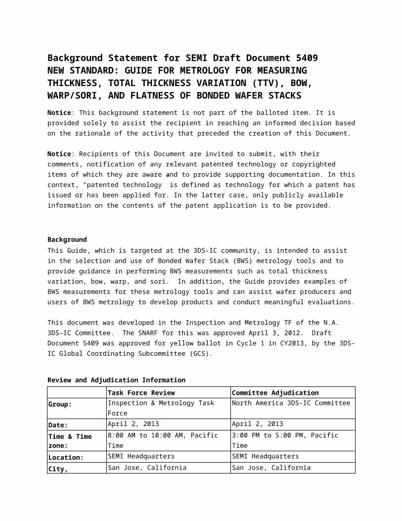
2.6 The measurements described in this Guide are on bonded wafer stacks with thickness in the range of 50 to 1550 μm.
2.7 The stacks considered include carrier and device wafers and bonding layers, including cases where there are more than two wafers in a stack. Bonded wafers may be classified as either temporarily bonded (i.e. a device to a carrier wafer) or permanently bonded. Temporary bonding uses a temporary adhesive; permanent bonding could be adhesive, oxide, metal-metal (e.g. Cu-Cu), or hybrid bonding. Two representative two-wafer stacks are depicted in Figures 1 and 2. The first stack (Figure 1) is a bonded pair of 775 µm thick wafers following TSV formation and the bonding operation. The second stack (Figure 2) is a bonded wafer stack with a top wafer thinned to ~50 µm, and bonded on top of a 775 µm wafer using a temporary adhesive.
This is a Draft Document of the SEMI International Standards program. No material on this page is to be construed as an official or adopted Standard or Safety Guideline. Permission is granted to reproduce and/or distribute this document, in whole or in part, only within the scope of SEMI International Standards committee (document development) activity. All other reproduction and/or distribution without the prior written consent of SEMI is prohibited.
Page 1 Doc. jn l SEMI
Semiconductor Equipment and Materials International3081 Zanker RoadSan Jose, CA 95134-2127Phone: 408.943.6900, Fax: 408.943.7943

DRAFTDocument Number:
Date: 5/8/23
Figure 1 Bonded Wafer Pair Following TSV Formation and Wafer Bonding Operation
Figure 2 Temporarily Bonded Wafer Pair--Device Wafer is Edge-Trimmed and Thinned
NOTICE: SEMI Standards and Safety Guidelines do not purport to address all safety issues associated with their use. It is the responsibility of the users of the Documents to establish appropriate safety and health practices, and determine the applicability of regulatory or other limitations prior to use.
3 Limitations3.1 While this Guide provides an overview on the use of several available techniques, it does not provide the level of detail typically available in Test Methods. For this purpose, SEMI documents are referenced that the user may find of interest. In addition, all suppliers may not follow SEMI standard measurement methods in their metrology procedures.
3.2 The information in this guide does not encompass the establishment of specific a methodology for such measurements but is only a guide to the user describing the various types of metrology including their capabilities and limitations.
3.3 This Guide describes metrologies that have been applied to a wafer stack composed of, at most, two wafers. Thus, the user is cautioned that the methods described may be limited with applied to wafer stacks consisting of more than two wafers.
4 Referenced Standards and Documents4.1 SEMI Standards and Safety Guidelines
SEMI M23 — Specification for Polished Monocrystalline Indium Phosphide Wafers
SEMI M43 — Guide for Reporting Wafer Nanotopography
SEMI M49 — Guide for Specifying Geometry Measurement Systems for Silicon Wafers for the 130 nm to 22 nm Technology Generations
SEMI M59 — Terminology for Silicon Technology
SEMI M65 — Specifications for Sapphire Substrates to Use for Compound Semiconductor Epitaxial Wafers
SEMI MF533 — Test Method for Thickness and Thickness Variation of Si Wafers
SEMI MF534 — Test Method for Bow of Silicon Wafers
This is a Draft Document of the SEMI International Standards program. No material on this page is to be construed as an official or adopted Standard or Safety Guideline. Permission is granted to reproduce and/or distribute this document, in whole or in part, only within the scope of SEMI International Standards committee (document development) activity. All other reproduction and/or distribution without the prior written consent of SEMI is prohibited.
Page 2 Doc. jn l SEMI
Semiconductor Equipment and Materials International3081 Zanker RoadSan Jose, CA 95134-2127Phone: 408.943.6900, Fax: 408.943.7943
DRAFTDocument Number:
Date: 5/8/23
SEMI MF657 — Standard Test Method for Measuring Warp and Total Thickness Variation on Silicon Slices and Wafers by a Non-contact Scanning Method
SEMI MF1390 — Standard Test Method for Measuring Warp on Silicon Wafers by Automated Non-Contact Scanning
SEMI MF1451 — Test Method for Measuring Sori on Silicon Wafers by Automated Non-Contact Scanning
SEMI MF1530 — Standard test method for Measuring Flatness, Thickness, and Thickness Variation on Silicon Wafers by Automated Non-Contact Scanning
NOTICE: Unless otherwise indicated, all documents cited shall be the latest published versions.
5 Terminology1: Refer to the SEMI Standards Compilation of Terms (COTs) for a list of the current Abbreviations, Acronyms, Definitions, and Symbols.
5.1 Abbreviations and Acronyms
5.1.1 AM — acoustic microscopy
5.1.2 BWS — bonded wafer stack
5.1.3 CD — critical dimension
5.1.4 CWS — chromatic white light sensor
5.1.5 CSI — coherence scanning interferometry
5.1.6 FAMM — focus/acquire/measure/move
5.1.7 FPD — focal plane deviation
5.1.8 HVM — high volume manufacturing
5.1.9 IR — infra-red
5.1.10 ISO — international organization for standardization
5.1.11 RPD — reference plane deviation
5.1.12 SLED — superluminescent light emitting diode
5.1.13 TIR — total indicated runout
5.1.14 TS — through-silicon via
5.1.15 TTV — total thickness variation
5.1.16 WLI — white light interferometry
5.2 Bonded Wafer Metrology Overview
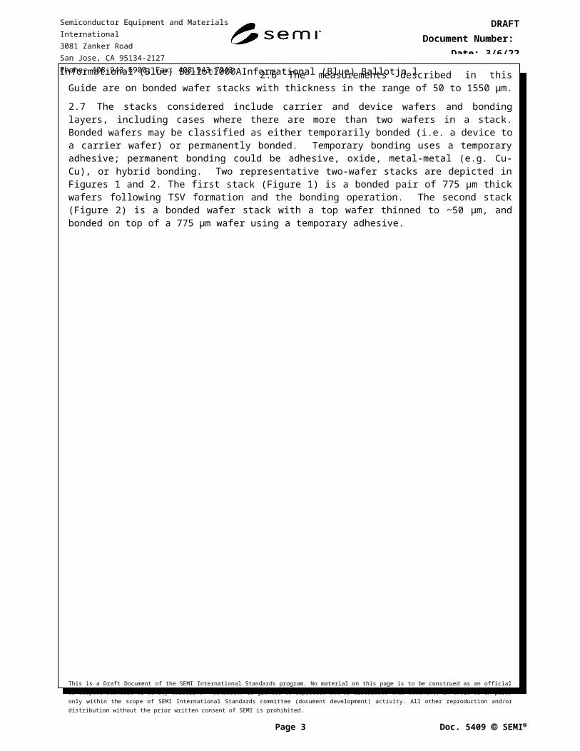
5.2.1 explanation of wafer metrology terms1 — the parameters primarily measured, wafer bow, warp, and sori need some explanation. Figure 3 shows schematic diagrams representing these terms.
5.2.1.1 bow — the deviation of the center point of the median surface of a free, unclamped wafer from a median surface reference plane established by three points equally spaced on a circle with diameter a specified amount less than the nominal diameter of the wafer; SEMI MF23 provides a standard test method for measuring the bow of a single wafer. Note that bow is a signed value. The method can be adapted to a bonded wafer stack.
5.2.1.2 warp — the difference between the most positive and most negative distances of the median surface of a free, unclamped wafer from a reference plane; SEMI M59 provides a standard test method for measuring the warp of a single wafer. Warp can be zero, even for a wafer with curvature, if the curves are mirror images of each other. SEMI MF657 measures median surface warp using a three-point back-surface reference plane, resulting in thickness variation being included in the warp value. The use of a median surface reference plane in SEMI MF1390
1 SEMI International Standards: Compilation of Terms (COT)
This is a Draft Document of the SEMI International Standards program. No material on this page is to be construed as an official or adopted Standard or Safety Guideline. Permission is granted to reproduce and/or distribute this document, in whole or in part, only within the scope of SEMI International Standards committee (document development) activity. All other reproduction and/or distribution without the prior written consent of SEMI is prohibited.
Page 3 Doc. jn l SEMI
Semiconductor Equipment and Materials International3081 Zanker RoadSan Jose, CA 95134-2127Phone: 408.943.6900, Fax: 408.943.7943

DRAFTDocument Number:
Date: 5/8/23
eliminates this effect. SEMI MF1390 provides a standard test method for measuring the warp of a single wafer. The method can be adapted to a bonded wafer stack.
5.2.1.3 sori — the algebraic difference between the most positive and most negative deviations of the front surface of a wafer that is not chucked from a reference plane that is a least squares fit to the front surface within the fixed quality area.
5.2.1.4 flatness — the deviation of the front surface, expressed in TIR or maximum FPD relative to a specified reference plane when the back surface of the wafer is ideally flat, as when pulled down by a vacuum onto an ideally flat chuck.
5.2.1.5 non-contact — metrology that allows a wafer to be measured without physical contact to the wafer surface, preventing contamination or damage to the wafer substrate.
5.2.1.6 chromatic white light sensor — a chromatic white light sensor (CWS) is based on the principal of confocal optics and relies on chromatic scanning. A lens is used that refracts white light differentially based on its wavelength in order to carry out distance measurements. Resolution depends on the intensity of reflected light.
5.2.1.7 interferometry — a technique that relies on the principal of superposition of multiple beams of light to determine the effect that a material has on the state (phase and amplitude) of the original light beam. It is this introduced phase difference that creates the interference pattern between the initially identical waves. If a single beam has been split along two paths, then the phase difference is diagnostic of anything that changes the phase along the paths. This could be a physical change in the path length itself or a change in the refractive index along the path.
5.2.1.8 gravity compensation for horizontally-supported wafers — unlike thickness and TTV measurements which are independent of how the wafer is held, bow and warp measurements are complicated not only by wafer stress but by how the wafer is supported and by gravity. Gravity causes substantial deformation of large diameter or thin wafers, whether they are supported at the edge or in the middle. Unless compensated, gravity will induce a large error in warp measurements. SEMI MF1390 describes three compensation approaches. One approach is to correct for the gravitational effect of warp measurements by inverting the wafer and measuring both the top and bottom surfaces of the wafer. Any differences between two values at the same site are due to the effect of gravity and can be used to correct for single-side measurements. Another approach is to use an analytical expression for gravitational deformation and subtract it from a single-side warp measurement2. Measurements obtained on representative wafers can also be performed and the gravity value determined.
5.2.1.8.1 In addition, the wafer can either rest on a chuck or be supported by three points (MF657).
5.2.1.9 gravity compensation for vertically supported-wafers — on tools that support the wafer vertically, effects due to gravity are negligible and therefore do not require compensation. Bow is only measured on one side so there is no need to invert the wafer. The manufacturing tolerance for sori is very low, such that a 300 mm diameter silicon wafer must achieve sori in the nanometer range in order to achieve the maximum yields in semiconductor device processing.
Figure 3Wafer Warp, Bow, and Sori Depictions2
2 W. R. Runyan, T. J. Schaffner, “Semiconductor Measurements and Instrumentation,” McGraw-Hill, 1998, pp. 218-221.
This is a Draft Document of the SEMI International Standards program. No material on this page is to be construed as an official or adopted Standard or Safety Guideline. Permission is granted to reproduce and/or distribute this document, in whole or in part, only within the scope of SEMI International Standards committee (document development) activity. All other reproduction and/or distribution without the prior written consent of SEMI is prohibited.
Page 4 Doc. jn l SEMI
Semiconductor Equipment and Materials International3081 Zanker RoadSan Jose, CA 95134-2127Phone: 408.943.6900, Fax: 408.943.7943

DRAFTDocument Number:
Date: 5/8/23
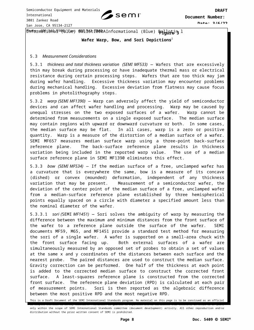
5.3 Measurement Considerations
5.3.1 thickness and total thickness variation (SEMI MF533) — Wafers that are excessively thin may break during processing or have inadequate thermal mass or electrical resistance during certain processing steps. Wafers that are too thick may jam during wafer handling. Excessive thickness variation may encounter problems during mechanical handling. Excessive deviation from flatness may cause focus problems in photolithography steps.
5.3.2 warp (SEMI MF1390) — Warp can adversely affect the yield of semiconductor devices and can affect wafer handling and processing. Warp may be caused by unequal stresses on the two exposed surfaces of a wafer. Warp cannot be determined from measurements on a single exposed surface. The median surface may contain regions with upward or downward curvature or both. In some cases, the median surface may be flat. In all cases, warp is a zero or positive quantity. Warp is a measure of the distortion of a median surface of a wafer. SEMI MF657 measures median surface warp using a three-point back-surface reference plane. The back-surface reference plane results in thickness variation being included in the reported warp value. The use of a median surface reference plane in SEMI MF1390 eliminates this effect.
5.3.3 bow (SEMI MF534) — If the median surface of a free, unclamped wafer has a curvature that is everywhere the same, bow is a measure of its concave (dished) or convex (mounded) deformation, independent of any thickness variation that may be present. Measurement of a semiconductor wafer, the deviation of the center point of the median surface of a free, unclamped wafer from a median-surface reference plane established by three hemispherical points equally spaced on a circle with diameter a specified amount less than the nominal diameter of the wafer.
5.3.3.1 sori (SEMI MF1451) — Sori solves the ambiguity of warp by measuring the difference between the maximum and minimum distances from the front surface of the wafer to a reference plane outside the surface of the wafer. SEMI documents MF59, M65, and MF1451 provide a standard test method for measuring the sori of a single wafer. A wafer is supported on a small-area chuck with the front surface facing up. Both external surfaces of a wafer are simultaneously measured by an opposed set of probes to obtain a set of values at the same x and y coordinates of the distances between each surface and the nearest probe. The paired distances are used to construct the median surface. Gravity correction can be performed. One half of the thickness at each point is added to the corrected median surface to construct the corrected front surface. A least-squares reference plane is constructed from the corrected front surface. The reference plane deviation (RPD) is calculated at each pair of measurement points. Sori is then reported as the algebraic difference between the most positive RPD and the most negative RPD.
6 Bonded Wafer Metrology Techniques6.1 Optical Techniques
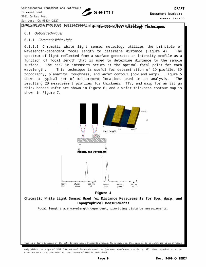
6.1.1 Chromatic White Light
6.1.1.1 Chromatic white light sensor metrology utilizes the principle of wavelength-dependent focal length to determine distance (Figure 4). The spectrum of light reflected from a surface generates an intensity profile as a function of focal length that is used to determine distance to the sample surface. The peak in intensity occurs at the optimal focal point for each wavelength. This technique is useful for determination of 2D profile, 3D topography, planarity, roughness, and wafer contour (bow and warp). Figure 5 shows a typical set of measurement locations used in an analysis. The resulting 2D measurement profiles for thickness, TTV, and warp for an 825 µm thick bonded wafer are shown in Figure 6, and a wafer thickness contour map is shown in Figure 7.
This is a Draft Document of the SEMI International Standards program. No material on this page is to be construed as an official or adopted Standard or Safety Guideline. Permission is granted to reproduce and/or distribute this document, in whole or in part, only within the scope of SEMI International Standards committee (document development) activity. All other reproduction and/or distribution without the prior written consent of SEMI is prohibited.
Page 5 Doc. jn l SEMI
Semiconductor Equipment and Materials International3081 Zanker RoadSan Jose, CA 95134-2127Phone: 408.943.6900, Fax: 408.943.7943

DRAFTDocument Number:
Date: 5/8/23
Figure 4Chromatic White Light Sensor Used for Distance Measurements for Bow, Warp, and Topographical
MeasurementsNOTE: Focal lengths are wavelength dependent, providing distance measurements.
Figure 5Data Collection Locations Showing Profile (a-d), and Points (A-I)
This is a Draft Document of the SEMI International Standards program. No material on this page is to be construed as an official or adopted Standard or Safety Guideline. Permission is granted to reproduce and/or distribute this document, in whole or in part, only within the scope of SEMI International Standards committee (document development) activity. All other reproduction and/or distribution without the prior written consent of SEMI is prohibited.
Page 6 Doc. jn l SEMI
Semiconductor Equipment and Materials International3081 Zanker RoadSan Jose, CA 95134-2127Phone: 408.943.6900, Fax: 408.943.7943

DRAFTDocument Number:
Date: 5/8/23
Figure 6Profile Measurements for Thickness, TTV, and Warp for 825 µm Thin Bonded Pair Wafer
Figure 7Wafer Map Results for 825 µm Thin Bonded Pair Wafer
6.1.2 Infra-red Interferometry
6.1.2.1 Interferometry is a technique in which light waves are superimposed to obtain information on surface profiles or displacements between two surfaces. Infra-red interferometry is useful for thickness measurements of substrates that are transparent in near IR light. Thickness measurements can be performed on single or multi-layer films, including adhesion layers in BWS. At each film interface, some incident light is reflected back to a detector.
6.1.2.2 When two light waves combine, the resulting pattern is determined by the phase difference between the two waves—waves that are in phase undergo constructive interference while waves that are out-of-phase undergo destructive interference. Typically, a beam of coherent light is split into two beams by a beam splitter. Each beam travels a different path and the two are recombined before arriving at the detector. The path difference, the difference in the distance traveled by each beam, creates a phase difference between them.
6.1.2.3 For a thin transparent medium, the reflection from the top surface interferes with the reflection from the bottom surface. For some wavelengths, the interference is constructive, and for others it is destructive. In general, the reflected intensity follows the Fabry-Perot equation (eq. 1):
This is a Draft Document of the SEMI International Standards program. No material on this page is to be construed as an official or adopted Standard or Safety Guideline. Permission is granted to reproduce and/or distribute this document, in whole or in part, only within the scope of SEMI International Standards committee (document development) activity. All other reproduction and/or distribution without the prior written consent of SEMI is prohibited.
Page 7 Doc. jn l SEMI
Semiconductor Equipment and Materials International3081 Zanker RoadSan Jose, CA 95134-2127Phone: 408.943.6900, Fax: 408.943.7943
DRAFTDocument Number:
Date: 5/8/23
R=| r1+r2 ei 2
1+r 1r2 ei 2 |2
(1)
6.1.2.4 Where r1 is the reflection coefficient at the first surface of the cavity, r2 is the reflection coefficient at the second surface, and δ = 2 π n l / λ, n is the index of refraction, l is the cavity thickness, and λ is the wavelength. Because of the complex exponential, the reflected intensity is periodic in δ. Since δ is proportional to optical frequency (c / λ), the reflected intensity is periodic in optical frequency with period c / 2nl, where n is the index of refraction, l is the layer thickness, and c is the speed of light in a vacuum. Then the basic procedure to measure the thickness is to: 1) measure the reflectance for a spectrum of wavelengths; 2) analyze the measured spectrum for a periodic intensity as a function of optical frequency; 3) calculate thickness from the period and index of refraction.
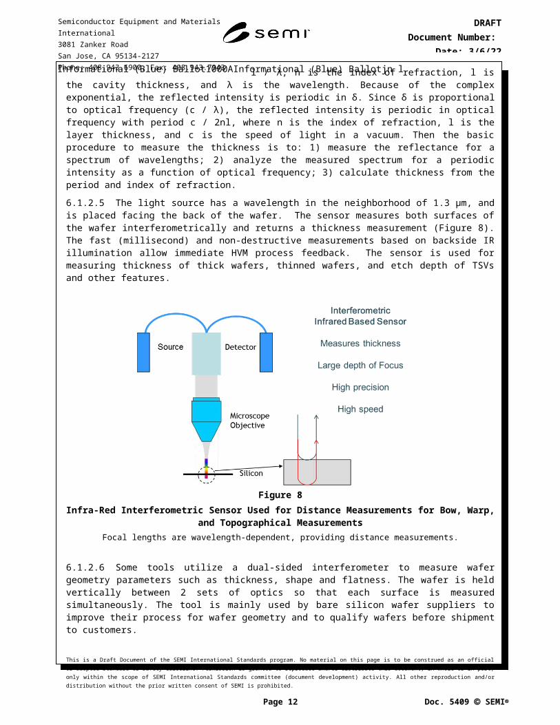
6.1.2.5 The light source has a wavelength in the neighborhood of 1.3 µm, and is placed facing the back of the wafer. The sensor measures both surfaces of the wafer interferometrically and returns a thickness measurement (Figure 8). The fast (millisecond) and non-destructive measurements based on backside IR illumination allow immediate HVM process feedback. The sensor is used for measuring thickness of thick wafers, thinned wafers, and etch depth of TSVs and other features.
Figure 8Infra-Red Interferometric Sensor Used for Distance Measurements for Bow, Warp, and Topographical
MeasurementsNOTE: Focal lengths are wavelength-dependent, providing distance measurements.
6.1.2.6 Some tools utilize a dual-sided interferometer to measure wafer geometry parameters such as thickness, shape and flatness. The wafer is held vertically between 2 sets of optics so that each surface is measured simultaneously. The tool is mainly used by bare silicon wafer suppliers to improve their process for wafer geometry and to qualify wafers before shipment to customers.
6.1.2.7 Wafer geometry data acquired in 3D is capable of providing nanotopography and wafer edge roll-off. Wafer manufacturing issues can affect geometry at the edge of the wafer, causing die defocus and CMP removal non-uniformity.
6.1.2.8 The thickness and warp of the two individual wafers in a bonded pair can be measured using interferometry utilizing the interference between the light reflected from the wafer and the light reflected from a moving mirror. The general scheme of such an interferometer is shown in Figure 9.
This is a Draft Document of the SEMI International Standards program. No material on this page is to be construed as an official or adopted Standard or Safety Guideline. Permission is granted to reproduce and/or distribute this document, in whole or in part, only within the scope of SEMI International Standards committee (document development) activity. All other reproduction and/or distribution without the prior written consent of SEMI is prohibited.
Page 8 Doc. jn l SEMI
Semiconductor Equipment and Materials International3081 Zanker RoadSan Jose, CA 95134-2127Phone: 408.943.6900, Fax: 408.943.7943
DRAFTDocument Number:
Date: 5/8/23
Figure 9Schematic View of an Interferometer System
NOTE: Beam 2, which is reflected from the bottom surface of the wafer, is delayed with respect to beam 1 reflected from the top surface. The delay between beam 1 and beam 2 is proportional to the thickness of the wafer. In a real experiment, the incident
beam is perpendicular to the surface of the wafer.
6.1.2.9 A SLED (superluminescent light-emitting diode) with a broad line width was used and retro-reflecting mirrors were mounted in a nano-motor stage. The dual-probe scheme for total thickness and warp measurement is shown in Figure 10.
Figure 10Dual Probe Scheme for the Measurement of the Thickness and Warp
6.1.2.10 In the dual-probe setup, each probe has a reference and a measurement arm. Light from each arm interferes with light from the scanning mirror to generate the first two interference signals in the upper probe. Similarly, light from the reference arm and the back surface of wafer produces the first two interference signals in the lower probe. The distance between the two probes can be determined using the known thickness of a block gauge. This information in conjunction with the two signals from the upper and lower probes makes it possible to measure the total thickness of the wafer. If the wafer surfaces are rough and/or the substrate is opaque to the incident light, the
This is a Draft Document of the SEMI International Standards program. No material on this page is to be construed as an official or adopted Standard or Safety Guideline. Permission is granted to reproduce and/or distribute this document, in whole or in part, only within the scope of SEMI International Standards committee (document development) activity. All other reproduction and/or distribution without the prior written consent of SEMI is prohibited.
Page 9 Doc. jn l SEMI
Semiconductor Equipment and Materials International3081 Zanker RoadSan Jose, CA 95134-2127Phone: 408.943.6900, Fax: 408.943.7943

DRAFTDocument Number:
Date: 5/8/23
dual probe is a good way to measure its thickness. A typical signal collected by an interferometer system on a bare Si wafer is shown in Figure 11. For warp measurement, the distance between the reference signal and the signal from the front surface of a wafer into the top probe is measured. In a warp measurement, a 300 mm blank wafer is used as the un-warped reference.
Figure 11Typical Signal from an Interferometer System
6.1.2.11 In Figure 12, TTV maps are shown with measurement locations (left) as well as 2D TTV (center) and 3D TTV (right) maps for an 825 µm two wafer stack. Typical wafer thickness results are shown in Figures 13-15 for a 1550 m thick two wafer stack.
Figure 1225-Point 2D and 3D Image Files of TTV for 825 µm Two Wafer Stack
This is a Draft Document of the SEMI International Standards program. No material on this page is to be construed as an official or adopted Standard or Safety Guideline. Permission is granted to reproduce and/or distribute this document, in whole or in part, only within the scope of SEMI International Standards committee (document development) activity. All other reproduction and/or distribution without the prior written consent of SEMI is prohibited.
Page 10 Doc. jn l SEMI
Semiconductor Equipment and Materials International3081 Zanker RoadSan Jose, CA 95134-2127Phone: 408.943.6900, Fax: 408.943.7943

DRAFTDocument Number:
Date: 5/8/23
Figure 131550 µm Two Wafer Stack –Results Showing Bottom Wafer Thickness Map
Figure 14Two Wafer Stack –Results Showing Top Wafer Warp Map
Figure 151550 µm Two Wafer Stack –Results Showing Top (Thinned) Wafer Thickness Map
This is a Draft Document of the SEMI International Standards program. No material on this page is to be construed as an official or adopted Standard or Safety Guideline. Permission is granted to reproduce and/or distribute this document, in whole or in part, only within the scope of SEMI International Standards committee (document development) activity. All other reproduction and/or distribution without the prior written consent of SEMI is prohibited.
Page 11 Doc. jn l SEMI
Semiconductor Equipment and Materials International3081 Zanker RoadSan Jose, CA 95134-2127Phone: 408.943.6900, Fax: 408.943.7943
DRAFTDocument Number:
Date: 5/8/23
6.1.3 Coherence Scanning Interferometry (CSI) or White Light Interferometry (WLI)
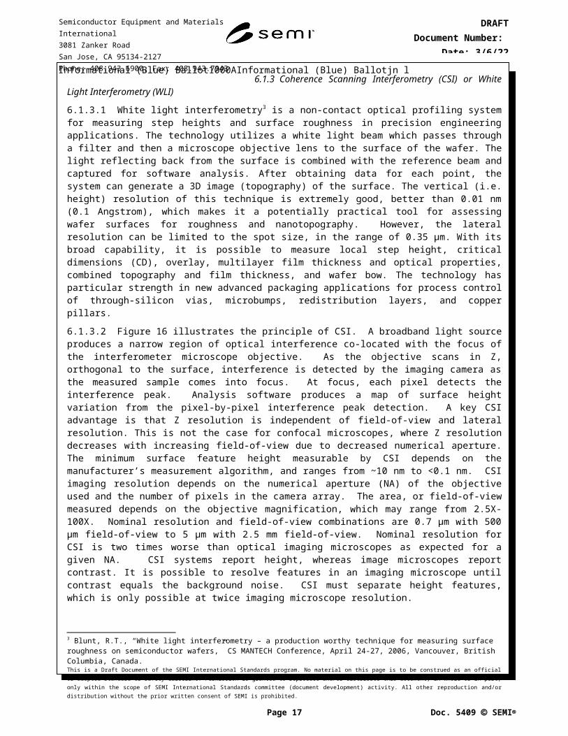
6.1.3.1 White light interferometry3 is a non-contact optical profiling system for measuring step heights and surface roughness in precision engineering applications. The technology utilizes a white light beam which passes through a filter and then a microscope objective lens to the surface of the wafer. The light reflecting back from the surface is combined with the reference beam and captured for software analysis. After obtaining data for each point, the system can generate a 3D image (topography) of the surface. The vertical (i.e. height) resolution of this technique is extremely good, better than 0.01 nm (0.1 Angstrom), which makes it a potentially practical tool for assessing wafer surfaces for roughness and nanotopography. However, the lateral resolution can be limited to the spot size, in the range of 0.35 μm. With its broad capability, it is possible to measure local step height, critical dimensions (CD), overlay, multilayer film thickness and optical properties, combined topography and film thickness, and wafer bow. The technology has particular strength in new advanced packaging applications for process control of through-silicon vias, microbumps, redistribution layers, and copper pillars.
6.1.3.2 Figure 16 illustrates the principle of CSI. A broadband light source produces a narrow region of optical interference co-located with the focus of the interferometer microscope objective. As the objective scans in Z, orthogonal to the surface, interference is detected by the imaging camera as the measured sample comes into focus. At focus, each pixel detects the interference peak. Analysis software produces a map of surface height variation from the pixel-by-pixel interference peak detection. A key CSI advantage is that Z resolution is independent of field-of-view and lateral resolution. This is not the case for confocal microscopes, where Z resolution decreases with increasing field-of-view due to decreased numerical aperture. The minimum surface feature height measurable by CSI depends on the manufacturer’s measurement algorithm, and ranges from ~10 nm to <0.1 nm. CSI imaging resolution depends on the numerical aperture (NA) of the objective used and the number of pixels in the camera array. The area, or field-of-view measured depends on the objective magnification, which may range from 2.5X-100X. Nominal resolution and field-of-view combinations are 0.7 µm with 500 µm field-of-view to 5 µm with 2.5 mm field-of-view. Nominal resolution for CSI is two times worse than optical imaging microscopes as expected for a given NA. CSI systems report height, whereas image microscopes report contrast. It is possible to resolve features in an imaging microscope until contrast equals the background noise. CSI must separate height features, which is only possible at twice imaging microscope resolution.
Figure 16Coherence Scanning Interferometer for the Measurement of Surface Topography
NOTE: Z height is measured at each pixel as the interferometric objective is scanned in Z and the camera detects the peak of the coherence envelope as shown.
3 Blunt, R.T., “White light interferometry – a production worthy technique for measuring surface roughness on semiconductor wafers,” CS MANTECH Conference, April 24-27, 2006, Vancouver, British Columbia, Canada.
This is a Draft Document of the SEMI International Standards program. No material on this page is to be construed as an official or adopted Standard or Safety Guideline. Permission is granted to reproduce and/or distribute this document, in whole or in part, only within the scope of SEMI International Standards committee (document development) activity. All other reproduction and/or distribution without the prior written consent of SEMI is prohibited.
Page 12 Doc. jn l SEMI
Semiconductor Equipment and Materials International3081 Zanker RoadSan Jose, CA 95134-2127Phone: 408.943.6900, Fax: 408.943.7943

DRAFTDocument Number:
Date: 5/8/23
6.1.3.3 CSI can measure polished and rough surfaces, as well as flatness to nm – to mm high stepped and sloped surfaces. When combined with image analysis software, CSI can measure and position three-dimensional features to sub-micron repeatability in X and Y, combined with sub-nanometer repeatability in Z. Typical applications are surface roughness (commercial tools provide industry standard results, but often lack ISO specified software bandpass filters), nanotopography, local step height, critical dimensions (CD) and overlay. The technology has particular strength in new advanced packaging applications for process control of through-silicon vias (TSVs), microbumps, redistribution layers, copper studs and pillars.
6.1.3.4 A major strength of CSI is ease-of-use and speed of measurement. Advanced tools incorporate autofocus and automation capabilities to speed the measurement process. Typically no special preparation is required of the measurement sample, if the sample is homogeneous and without film layers. Microbump/pillar measurements have been demonstrated in production with 0.5 second Focus/Acquire/Measure/Move (FAMM) times, while maintaining nanometer Z performance. Laboratory tools can experience one to five-minute FAMM’s primarily due to instrument set up time.
6.1.3.5 The presence of films and films stacks are both an opportunity and technology limitation of CSI. Present CSI algorithms are limited to reliably measuring in the presence of films to thicknesses greater than 1.5μm optical thickness (thickness times index of refraction). Some manufacturers claim this capability down to 1-μm optical thickness. Reported measurement results are film thickness (if the index of refraction is known), surface profile of the top and also the bottom of the film. Advanced work is occurring to measure features in thin film structures, improved CD and other edge of resolution features. As these technologies emerge new applications will be possible. When films are less than the measurable optical thickness unpredictable errors occur in the measured data, and the data is unreliable in Z height.
6.1.3.6 Measuring non-homogeneous materials limits CSI accuracy. CSI measures Z height by measuring interferometric phase. Phase is dependent on the material measured. Insulators experience a constant 180° phase shift, whereas conductors and semi-conductors induce varying phase shifts. These phase shifts appears as surface topography errors up to 10’s of nanometers. It is possible to correct for these by identifying material types by regions and region-by-region apply a correction factor. Some manufacturers have seen success correcting algorithmically but this has seen little commercial utilization. For process control, phase change on reflection is a constant offset and therefore can be ignored when process variation is being tracked when absolute values are not critical.
6.1.3.7 CSI requires minimal to no surface preparation. Rapid measurements, nanometer level Z resolution and optical level image resolution make it a preferred tool for many applications. Measurement errors due to films and phase change of reflection of non-homogeneous materials are major limitations for applications based on semiconductor processes.
6.1.3.8 Five sets of 49 wafer bow measurements (top and bottom) for a 1550 μm bonded wafer pair are averaged in Figure 17, and the 3 sigma standard deviation is shown in Figure 18.
This is a Draft Document of the SEMI International Standards program. No material on this page is to be construed as an official or adopted Standard or Safety Guideline. Permission is granted to reproduce and/or distribute this document, in whole or in part, only within the scope of SEMI International Standards committee (document development) activity. All other reproduction and/or distribution without the prior written consent of SEMI is prohibited.
Page 13 Doc. jn l SEMI
Semiconductor Equipment and Materials International3081 Zanker RoadSan Jose, CA 95134-2127Phone: 408.943.6900, Fax: 408.943.7943

DRAFTDocument Number:
Date: 5/8/23
Figure 17Results for 49 Point Dynamic Repeat Bow Measurement on a 1550 m Bonded Wafer Pair (3, 5 Repeats)—
Average Bow of Top and Bottom Measurement (3 Point Suspension)
Figure 18Results for 49 Point Dynamic Repeat Bow Measurement on a 1550 m Bonded Wafer Pair (3, 5 Repeats)—
Average Standard Deviation of Top and Bottom Measurement (3 Point Suspension)
6.1.4 Laser Profiling
6.1.4.1 The diagram in Figure 19 demonstrates the principal of laser profiling with a single optical head where the laser is focused first on the top and then on the bottom of the wafer. The laser peak positions that are used to determine the wafer thickness are also shown.
6.1.4.2 Two focused laser beams can also be used, one focused on the top and the other on the bottom of the wafer stack (Figure 20). The measurement is made by moving the focus position from the surface of the top wafer to the top surface of the bottom wafer. The laser can be focused in the objective to a spot as small as 1 m. The dual optical measurement system provides accurate wafer thickness measurements independent of material properties, especially useful for patterned or bumped wafers, GaAs and other wafer types, and after back grinding and dicing. Laser profiling provides thickness resolution of approximately 0.1 m and has also been applied to TTV, bow, warp, and surface roughness.
This is a Draft Document of the SEMI International Standards program. No material on this page is to be construed as an official or adopted Standard or Safety Guideline. Permission is granted to reproduce and/or distribute this document, in whole or in part, only within the scope of SEMI International Standards committee (document development) activity. All other reproduction and/or distribution without the prior written consent of SEMI is prohibited.
Page 14 Doc. jn l SEMI
Semiconductor Equipment and Materials International3081 Zanker RoadSan Jose, CA 95134-2127Phone: 408.943.6900, Fax: 408.943.7943

DRAFTDocument Number:
Date: 5/8/23
OPTICAL THICKNESS MODULE
BEAM EXPANDER
BEAM SPLITTER
OBJECTIVE
MEASUREMENT SAMPLE
SIGNAL DETECTION MODULE
OPTICAL FIBER
DETECTOR
PINHOLE FOCUSING LENS
BOTTOM OF WAFER
TOP OF WAFER
Figure 19Principle of Single Beam Wafer Thickness Measurement System Showing Wafer Top and Bottom Signal
Peak Positions
Figure 20Dual-Beam Thickness Description
6.1.4.3 The plot in Figure 21 is a plot of the laser focused on the wafer surface as well as a glass surface. The difference in the “in-focus” locations equals the thickness of the glass.
This is a Draft Document of the SEMI International Standards program. No material on this page is to be construed as an official or adopted Standard or Safety Guideline. Permission is granted to reproduce and/or distribute this document, in whole or in part, only within the scope of SEMI International Standards committee (document development) activity. All other reproduction and/or distribution without the prior written consent of SEMI is prohibited.
Page 15 Doc. jn l SEMI
Semiconductor Equipment and Materials International3081 Zanker RoadSan Jose, CA 95134-2127Phone: 408.943.6900, Fax: 408.943.7943

DRAFTDocument Number:
Date: 5/8/23
Figure 21Example Plot Thickness Measurement
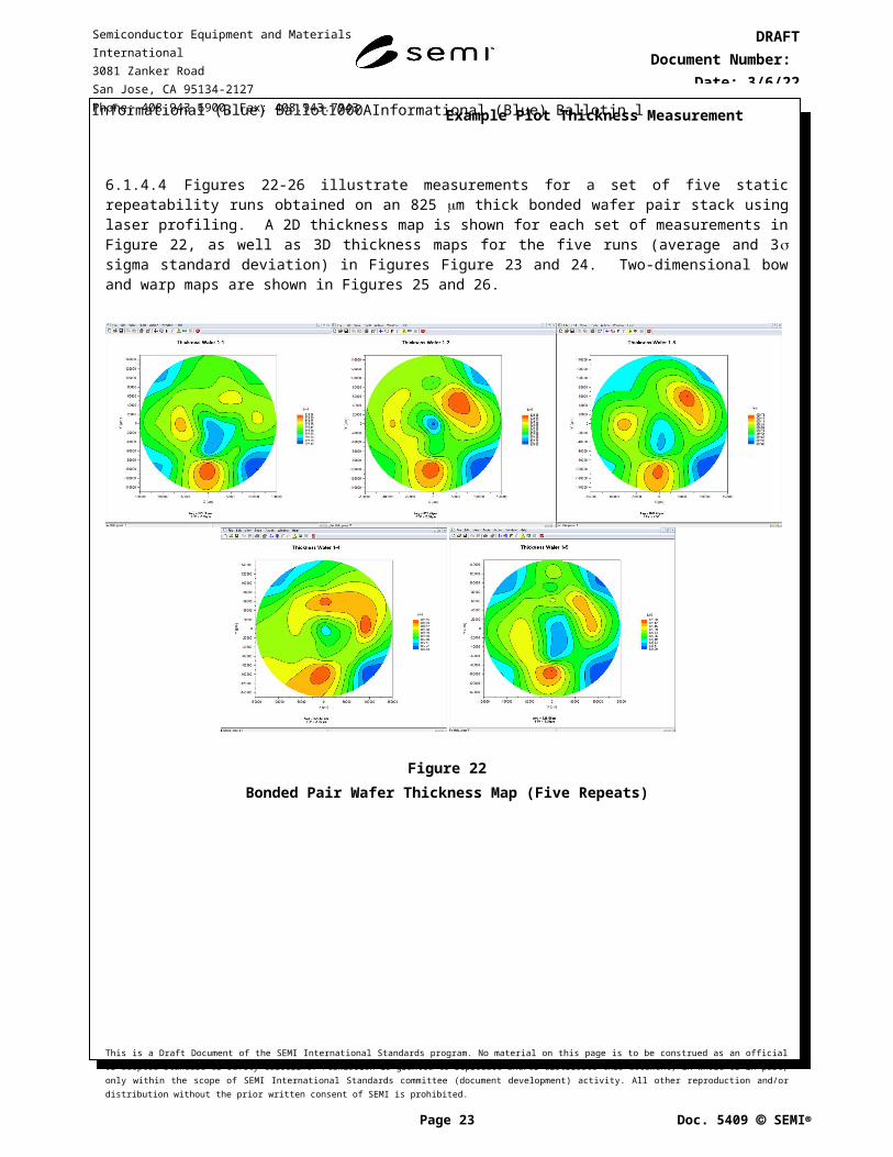
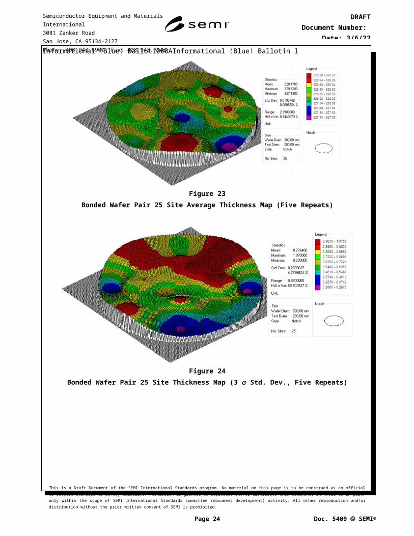
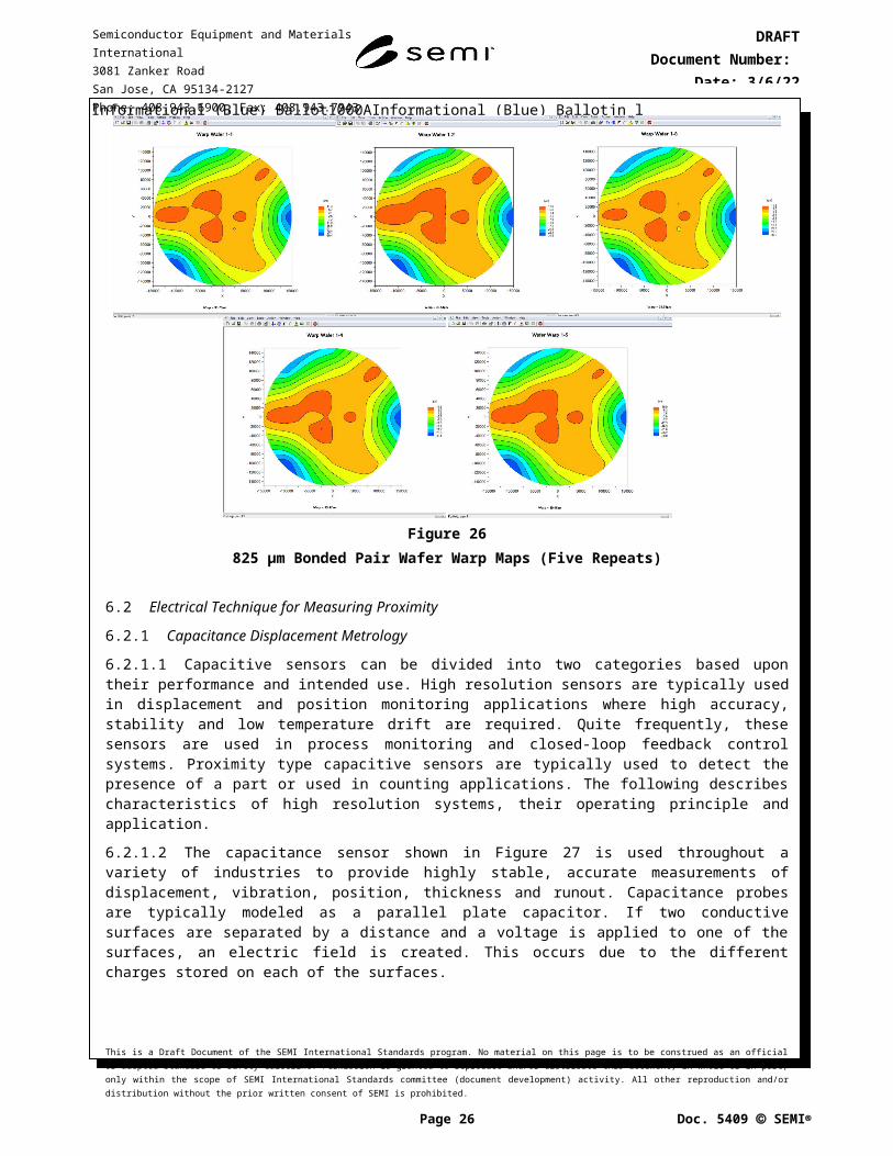
6.1.4.4 Figures 22-26 illustrate measurements for a set of five static repeatability runs obtained on an 825 m thick bonded wafer pair stack using laser profiling. A 2D thickness map is shown for each set of measurements in Figure 22, as well as 3D thickness maps for the five runs (average and 3 sigma standard deviation) in Figures Figure 23 and 24. Two-dimensional bow and warp maps are shown in Figures 25 and 26.
This is a Draft Document of the SEMI International Standards program. No material on this page is to be construed as an official or adopted Standard or Safety Guideline. Permission is granted to reproduce and/or distribute this document, in whole or in part, only within the scope of SEMI International Standards committee (document development) activity. All other reproduction and/or distribution without the prior written consent of SEMI is prohibited.
Page 16 Doc. jn l SEMI
Semiconductor Equipment and Materials International3081 Zanker RoadSan Jose, CA 95134-2127Phone: 408.943.6900, Fax: 408.943.7943
DRAFTDocument Number:
Date: 5/8/23
Figure 22Bonded Pair Wafer Thickness Map (Five Repeats)
Figure 23Bonded Wafer Pair 25 Site Average Thickness Map (Five Repeats)
This is a Draft Document of the SEMI International Standards program. No material on this page is to be construed as an official or adopted Standard or Safety Guideline. Permission is granted to reproduce and/or distribute this document, in whole or in part, only within the scope of SEMI International Standards committee (document development) activity. All other reproduction and/or distribution without the prior written consent of SEMI is prohibited.
Page 17 Doc. jn l SEMI
Semiconductor Equipment and Materials International3081 Zanker RoadSan Jose, CA 95134-2127Phone: 408.943.6900, Fax: 408.943.7943

DRAFTDocument Number:
Date: 5/8/23
Figure 24Bonded Wafer Pair 25 Site Thickness Map (3 Std. Dev., Five Repeats)
Figure 25Bonded Pair Wafer Bow Map (Five Repeats)
This is a Draft Document of the SEMI International Standards program. No material on this page is to be construed as an official or adopted Standard or Safety Guideline. Permission is granted to reproduce and/or distribute this document, in whole or in part, only within the scope of SEMI International Standards committee (document development) activity. All other reproduction and/or distribution without the prior written consent of SEMI is prohibited.
Page 18 Doc. jn l SEMI
Semiconductor Equipment and Materials International3081 Zanker RoadSan Jose, CA 95134-2127Phone: 408.943.6900, Fax: 408.943.7943

DRAFTDocument Number:
Date: 5/8/23
Figure 26825 µm Bonded Pair Wafer Warp Maps (Five Repeats)
6.2 Electrical Technique for Measuring Proximity
6.2.1 Capacitance Displacement Metrology
6.2.1.1 Capacitive sensors can be divided into two categories based upon their performance and intended use. High resolution sensors are typically used in displacement and position monitoring applications where high accuracy, stability and low temperature drift are required. Quite frequently, these sensors are used in process monitoring and closed-loop feedback control systems. Proximity type capacitive sensors are typically used to detect the presence of a part or used in counting applications. The following describes characteristics of high resolution systems, their operating principle and application.
6.2.1.2 The capacitance sensor shown in Figure 27 is used throughout a variety of industries to provide highly stable, accurate measurements of displacement, vibration, position, thickness and runout. Capacitance probes are typically modeled as a parallel plate capacitor. If two conductive surfaces are separated by a distance and a voltage is applied to one of the surfaces, an electric field is created. This occurs due to the different charges stored on each of the surfaces.
This is a Draft Document of the SEMI International Standards program. No material on this page is to be construed as an official or adopted Standard or Safety Guideline. Permission is granted to reproduce and/or distribute this document, in whole or in part, only within the scope of SEMI International Standards committee (document development) activity. All other reproduction and/or distribution without the prior written consent of SEMI is prohibited.
Page 19 Doc. jn l SEMI
Semiconductor Equipment and Materials International3081 Zanker RoadSan Jose, CA 95134-2127Phone: 408.943.6900, Fax: 408.943.7943

DRAFTDocument Number:
Date: 5/8/23
Figure 27Typical Capacitance Sensor
6.2.1.3 Capacitance refers to the ability of the surfaces to hold a charge. In a typical sensor system the probe is one of the plates and the target being measured is the other plate. If a constant current is applied, the capacitance change can be monitored as a linear voltage charge related to the distance between the plates (Figure 28).
Figure 28Typical Capacitance Sensor Measurement Parameters
6.2.1.4 This distance, or gap, is a function of the area of the capacitance sensor according to the following equation (Eq. 2):
C=ε πrd
2
(2)
Where capacitance is the area of sensor, A = r2 times the dielectric constant of air, divided by the gap, d.
6.2.1.5 From this relationship, capacitance is directly proportional to the area of the sensor and the dielectric property of the material between the sensor and target (typically air). The greater the area of the capacitance sensor the larger the measurement range, or gap. If it is assumed that the area and the dielectric constant between the plates remain constant for a specific probe, any change in capacitance is inversely proportional to the change in distance between the probe and target being measured and this change is converted to a voltage for monitoring. The amount of voltage output change for a given distance change is commonly referred to as the sensitivity of the system. For example, if a distance change of 1 mm corresponds to a voltage output change of 10 V the sensitivity would be 1 mm/10 V, or 0.1 mm/V.
This is a Draft Document of the SEMI International Standards program. No material on this page is to be construed as an official or adopted Standard or Safety Guideline. Permission is granted to reproduce and/or distribute this document, in whole or in part, only within the scope of SEMI International Standards committee (document development) activity. All other reproduction and/or distribution without the prior written consent of SEMI is prohibited.
Page 20 Doc. jn l SEMI
Semiconductor Equipment and Materials International3081 Zanker RoadSan Jose, CA 95134-2127Phone: 408.943.6900, Fax: 408.943.7943

DRAFTDocument Number:
Date: 5/8/23
6.2.2 Capacitance Sensors Electric Field
6.2.2.1 A typical high performance capacitance sensor consists of three basic elements: the sensor tip, the guard and the ground shell. Figure 29 illustrates a typical capacitance probe. When a voltage is applied to the sensor tip, an electric field is established between it and any other local conductive material. To maintain accuracy and linearity it is essential that the electric field in the measurement area be linear, directed toward the target, and not distorted. To protect this field, each capacitive sensor has a guard electrode. This creates an additional field around the probe sensing tip that is driven at the same phase and voltage potential as the sensor. By being equal, the auxiliary field protects the area from becoming warped and cancels any stray capacitance between the two elements.
6.2.2.2 Because the ground shell is at a different potential than the guard, a partial distortion of the guard field to the ground shell occurs. Although undesirable, the distortion of the guard is acceptable as long as the sensor tip field remains linear. For best performance, the width of the guard should be at least 2X the system measurement range.
Figure 29Capacitance Sensor Field
6.2.2.3 Capacitance probes should be designed with sufficient guard electrodes to protect the sensing area under normal operating conditions. This probe’s range should not be greater than the width of the guard electrode or poor linearity will result.
6.2.2.4 In addition to improving linearity and accuracy, the guard is also used to reduce noise and external interference. Each capacitance probe is driven by a low noise coaxial cable. The shield of the cable is used to deliver the voltage to the guard, at the same voltage and phase. This eliminates any stray capacitance that might be created between the center conductor and the shield of the cable, or any other part that may be close to the cable. By design, this protection significantly reduces external influences from RFI and EMI. It is important to note that ordinary coaxial cable usually does not provide adequate protection or shielding for the system and special cable is generally required.
6.2.3 Characteristics of Capacitive Sensors
6.2.3.1 Non-Contact
6.2.3.1.1 Capacitive displacement sensors are non-contact by design. That is, they are able to precisely measure the position or displacement of an object without touching it. Because of this the object being measured will not be distorted or damaged and target motions will not be dampened. Additionally, they can measure high frequency motions because no part of the sensor needs to stay in contact with the object, making them ideal for vibration measurements or high speed production line applications.
6.2.3.2 Range/Standoff Distance
6.2.3.2.1 As mentioned above, the range of a capacitance sensor is dictated by the diameter, or area, of the sensor. The larger the area, the larger the measurement range. Measurement range is typically specified starting when the probe is touching the target. At this point the output from the amplifier is 0 V. When the gap is increased to equal the full scale measurement range of the capacitive system the amplifier output is 10 V (Vdc). In theory, the probe can operate anywhere between these two extremes, however, it is not recommended to operate below 10% of the gap. Thus, the ideal operating or standoff distance is between 5 V and 7 Vdc, permitting the target to move closer to or
This is a Draft Document of the SEMI International Standards program. No material on this page is to be construed as an official or adopted Standard or Safety Guideline. Permission is granted to reproduce and/or distribute this document, in whole or in part, only within the scope of SEMI International Standards committee (document development) activity. All other reproduction and/or distribution without the prior written consent of SEMI is prohibited.
Page 21 Doc. jn l SEMI
Semiconductor Equipment and Materials International3081 Zanker RoadSan Jose, CA 95134-2127Phone: 408.943.6900, Fax: 408.943.7943

DRAFTDocument Number:
Date: 5/8/23
further away from the probe without going out of range. Figure 30 is a simplified diagram showing range, output voltage and recommended standoff for a typical capacitance sensor.
Figure 30Capacitance Probe Operating Range
6.2.3.3 Resolution
6.2.3.3.1 The resolution of a displacement sensor is defined as the smallest amount of distance change that can be reliably measured by a specific system. Capacitance sensors offer extremely high resolution and stability, often exceeding that of complex laser interferometer systems. Because of their ability to detect such small motions, they have been successfully used in many demanding measurement applications including computer disk drive runout, microscope focusing and nano-positioning within highly complex photolithography tools.
6.2.3.3.2 The primary factor in determining resolution is the system’s electrical noise. If the distance between the sensor and target is constant, the voltage output will still fluctuate slightly due to the “white” noise of the system. It is assumed that, without external signal processing, one cannot detect a shift in the voltage output of less than the random noise of the instrument. Because of this, most resolution values are presented based on the peak-to-peak value of noise and can be represented by the following formula: Resolution = Sensitivity × Noise.
6.2.3.3.3 Sensitivity is simply the measurement range divided by the voltage output swing of the capacitance amplifier, that for a fixed sensitivity the resolution is solely dependent upon the noise of the system, so that the lower the noise, the better the resolution.
6.2.3.3.4 It is important to note that some manufacturers specify resolution based on peak or rms noise, resulting in claims that are 2X and 6X respectively better than peak-to-peak. Although an acceptable method, it is somewhat misleading as most users do not have the ability to measure voltage changes less than the peak-to-peak noise value.
6.2.3.4 Bandwidth
6.2.3.4.1 The bandwidth, or cutoff frequency, of a system is typically defined as the point where the output is dampened by 3 db. This is approximately equal to an output voltage drop of 30% of the actual value. In other words, if a target is vibrating with an amplitude of 1 mm at 5 kHz and the bandwidth of the capacitance sensor is 5 kHz the actual sensor output would be 1 mm × 70% = 0.7 mm.
6.2.3.5 Push or Range Extension
6.2.3.5.1 Typical capacitive amplifier systems operate over a specific capacitance range, limiting their ability to measure large motions or operate at comfortable standoff distances. To overcome this problem some suppliers use a proprietary circuit that, with minor component modifications, can be adjusted to change the range and meet a wider variety of customer requirements. For example, a small diameter probe with a ½ mm measurement range can be “pushed” to have a measurement range of 1 mm or even 2 mm. This allows capacitive probes to be used in applications where space is limited or the target being measured is small. It is important to note, however, that a pushed probe should have a guard width sufficient enough to maintain the performance required, as mentioned
This is a Draft Document of the SEMI International Standards program. No material on this page is to be construed as an official or adopted Standard or Safety Guideline. Permission is granted to reproduce and/or distribute this document, in whole or in part, only within the scope of SEMI International Standards committee (document development) activity. All other reproduction and/or distribution without the prior written consent of SEMI is prohibited.
Page 22 Doc. jn l SEMI
Semiconductor Equipment and Materials International3081 Zanker RoadSan Jose, CA 95134-2127Phone: 408.943.6900, Fax: 408.943.7943
DRAFTDocument Number:
Date: 5/8/23
above. Additionally, pushing a sensor also amplifies system noise, reducing probe resolution. Noise increase is proportional to push; 2 × Push = 2 × Noise
6.2.3.6 Spatial Resolution
6.2.3.6.1 The field established between a capacitance probe tip and measured object is typically larger than the diameter of the probe tip (Figure 31). This is because there is an epoxy gap between the tip and guard elements. The field diameter is equal to D plus 1X the epoxy gap. When obtaining measurements, capacitance probes provide a distance equal to the average surface location within the spot area. They are not capable of accurately detecting the position of features smaller than the size of the spot. However, they can repeatedly measure rough surfaces. Because of this, the probe tip should always be 25% smaller than the smallest feature targeted for measurement. Smaller sensors can distinguish smaller features on an object.
Figure 31Effective Spot Size of a Capacitive Sensor
6.2.3.7 Linearity
6.2.3.7.1 Capacitance sensors may have an output of 0–10 Vdc over the full scale measurement range (FSR). In an ideal world this output would be perfectly linear and not deviate from a straight line at any point. However, in reality there are slight deviations from linearity. Typically, linearity is specified as a percentage of the Full Scale Measurement range. During calibration the output from the amplifier is compared to the output of a highly precise standard and differences are noted. Some capacitance systems exceed ±0.05% FSR with some achieving ±0.01% or better.
6.2.3.7.2 Accuracy is a function of linearity, resolution, temperature stability and drift, with linearity being the majority contributor. Calibration reports provide data that can be used to correct for the non-linearity of a system with inexpensive computers and correction software. Digital correction typically yields a linearity of ±0.01% or better.
6.2.3.8 Stability
6.2.3.8.1 Stability is a function of a variety of different internal and external factors. For short term or relative measurement applications stability is typically not an issue. However, if high accuracy is required over a long period of time, care must be taken when designing fixtures, selecting components and specifying materials of construction.
6.2.3.8.2 Temperature is typically the biggest factor that affects stability. Temperature swings not only cause electronic drift but can also cause fixture and probe expansion and contraction. For critical applications high-quality capacitors, resistors and inductors specifically designed for stability to minimize the electronic drift should be used. To minimize mechanical drift, probes can be manufactured from special low thermal coefficient materials such as Invar. Thermal correction coefficients can also be provided and used for real-time compensation.
6.2.3.8.3 Active capacitance probe systems should never be used in high stability applications because any localized temperature change surrounding the sensor will result in drift.
This is a Draft Document of the SEMI International Standards program. No material on this page is to be construed as an official or adopted Standard or Safety Guideline. Permission is granted to reproduce and/or distribute this document, in whole or in part, only within the scope of SEMI International Standards committee (document development) activity. All other reproduction and/or distribution without the prior written consent of SEMI is prohibited.
Page 23 Doc. jn l SEMI
Semiconductor Equipment and Materials International3081 Zanker RoadSan Jose, CA 95134-2127Phone: 408.943.6900, Fax: 408.943.7943
DRAFTDocument Number:
Date: 5/8/23
6.2.3.9 Calibration
6.2.3.9.1 For low-end proximity sensors calibration is typically not important because linearity of the sensor is not critical. Most high performance systems are, by design, inherently linear to approximately ±0.1% of the full scale measurement range. Some capacitance manufacturers offer sensors with this performance, however, they are typically not suitable for high precision applications. During calibration, the manufacturer adjusts circuit gain, offset, and typically performs a proprietary linearity adjustment. Improved performance can be obtained by adding adjustable break point linearization circuitry within the amplifier circuit or by providing digital correction.
6.2.3.9.2 During calibration the output of the amplifier verses position of a target is recorded. A best fit straight line is generated based on this data. Each recorded point is then compared to the generated straight line and the percent deviation is calculated and plotted. Based upon the results adjustments can be made to improve the deviation to within acceptable limits.
6.2.3.10 Applying Capacitive Probes
6.2.3.10.1 Target Material and Grounding
6.2.3.10.1.1 A capacitance measurement system mimics a parallel plate capacitor with the sensor as one plate and the target being measured the other. To create the electric field between the two plates the target must be made of a conductive material. The composition or thickness of the target is not important, allowing them to be used in many applications not suitable for eddy current type sensors. In fact, the surface can even be a few hundred ohm-cm.
6.2.3.10.1.2 To complete the capacitance circuit the target should be grounded back to the amplifier. For optimal performance a conductive path is required, however, capacitive coupled targets can work well if the capacitance is 0.01 µf or higher. An example of a capacitively-coupled target is a shaft rotating on air bearings. In theory, air bearings are non-contact but the gap between elements is small, and their area is relatively large, creating a high capacitance path. Thousands of successful applications world-wide have been installed with this type of ground.
6.2.3.10.1.3 If the target is poorly grounded, the system is susceptible to external noise and interference. Care should be taken when designing the ground return path.
6.2.3.11 Target Size
6.2.3.11.1 The lines of flux in the electric field established between the probe and target always leave the capacitance sensor normal (90°) to its surface and always enter the target normal to its surface. If the target being measured is large enough, and the sensor is within range, the field within the sensing area will be consistent and linear. If the target is not large enough to support the field it will tend to wrap around the edge and enter normal to the target side (Figure 32). This field distortion will create measurement errors by degrading the sensor linearity and changing its measurement range. Because of this the original factory calibration can no longer be used and an in-place calibration is required, however, accuracy may still be compromised.
Figure 32Field Distortion from an Insufficient Target Size
This is a Draft Document of the SEMI International Standards program. No material on this page is to be construed as an official or adopted Standard or Safety Guideline. Permission is granted to reproduce and/or distribute this document, in whole or in part, only within the scope of SEMI International Standards committee (document development) activity. All other reproduction and/or distribution without the prior written consent of SEMI is prohibited.
Page 24 Doc. jn l SEMI
Semiconductor Equipment and Materials International3081 Zanker RoadSan Jose, CA 95134-2127Phone: 408.943.6900, Fax: 408.943.7943

DRAFTDocument Number:
Date: 5/8/23
6.2.3.11.2 Targets that are too small to support the electric field can also provide false displacement signals from lateral motions. Capacitive sensors are typically used to measure the gap or movement in the direction of the sensor axis. If the target is large enough any lateral motion will not distort the electric field, however, if the field is wrapped around the target any lateral motion will change the shape of the field causing a change in output even if the gap remains constant. As a general rule, the target should be 30-50% larger than the capacitance sensor.
6.2.3.12 Target Shape
6.2.3.12.1 Capacitance probes will measure the average distance to the target under the area of the sensor. If a tilted or curved target is being measured the electric field will be distorted and the accuracy compromised. When sensors are calibrated to a flat target the output voltage is theoretically zero when the probe is in contact with the target. This is not true when measuring curved or tilted surfaces because the surface prevents the probe from full target contact. The result will be a shift in the zero point from its original calibration which will be reflected as an offset in the measurement, not a sensitivity change. To overcome both issues an in-place calibration is possible to correct for the sensitivity change, however, the sensor measurement range may be reduced. As a general rule, a curved target should be 10 times larger in diameter than the sensing element of the capacitance sensor.
6.2.3.13 Spatial Resolution
6.2.3.13.1 Capacitance sensors have a relatively large sensing area in relationship to their measurement range. As mentioned above, these types of sensors take an average measurement to the surface in question. If this surface has features that are smaller than the sensing element the feature may not be detected or the sensor output may not respond accordingly. Figure 33 shows how the probe size can affect the sensor output when measuring a stepped object, demonstrating sharper voltage changes from a smaller diameter sensor (Sensor C).
Figure 33Spatial Resolution
6.2.3.13.2 Similarly, the output will depend on the surface roughness. If the roughness changes over an area the output from the capacitance sensor will change when the target translates beneath the probe because the average distance to the surface has changed. The amount of sensor output shift will depend on the magnitude of the surface roughness.
6.2.3.14 Environmental Conditions
6.2.3.14.1 Capacitance changes as the distance to the target changes and also depends upon the dielectric property of the material in the gap. Because of this, it is important that there is a homogeneous, non-conductive material between the probe and target. In most applications, this material is air, however, many times oil or some other dielectric fluid is successfully used. If it is not homogeneous, or if the dielectric properties in the gap change, then accuracy will be affected. This is typically not a problem for changing air properties because the effects are small.
This is a Draft Document of the SEMI International Standards program. No material on this page is to be construed as an official or adopted Standard or Safety Guideline. Permission is granted to reproduce and/or distribute this document, in whole or in part, only within the scope of SEMI International Standards committee (document development) activity. All other reproduction and/or distribution without the prior written consent of SEMI is prohibited.
Page 25 Doc. jn l SEMI
Semiconductor Equipment and Materials International3081 Zanker RoadSan Jose, CA 95134-2127Phone: 408.943.6900, Fax: 408.943.7943
DRAFTDocument Number:
Date: 5/8/23
For instance, the dielectric constant of air changes by ~1.4 ppm/1% of relative humidity. This represents a potential offset in the senor output of less than 1 mV with a relative humidity change of 50%. Care must be taken to avoid dielectric changes from other materials and ensure that dirt and debris do not accumulate in the capacitive probe gap.
6.2.3.14.2 The most common environmental problem that can affect the accuracy of a capacitive sensor is temperature. Not only do the electronics exhibit temperature drift but also expansion and contraction of the probe and fixturing physically changes the probe gap. Custom probes manufactured of highly stable materials, such as Invar, are available for extreme stability applications. It is also possible to adjust the temperature coefficient of components for custom high-stability applications.
6.2.3.15 Advantages and Disadvantages
6.2.3.16 Advantages
6.2.3.16.1 As with any sensing technology, capacitive systems have both advantages and disadvantages. Perhaps their greatest attribute is their ability to resolve measurements below one micro-inch (< 25 nm), at a fraction of the cost of other high performance technologies. Most are "passive" by design allowing them to be used in extreme environments while still maintaining stability. Sensors can be easily customized, allowing them to be adapted into a variety of applications or settings. They are immune to target composition and work equally well on all conductive targets, unlike eddy current probes. They are largely immune to ultrasonic noise, electromagnetic fields, lighting conditions, humidity and temperature.
6.2.3.17 Disadvantages
6.2.3.17.1 Capacitance technology dictates that the probe be mounted close to the target. This increases the probability of crashing the sensor or damaging the material being measured. Some suppliers have provisions to extend the measurement range and standoff of the sensor, however, this distance is rarely greater than 15 mm.
6.2.3.17.2 Capacitance sensors should also be kept clean. Dirt or other foreign debris can cause an offset in the measurement so frequent cleaning may be required depending on the application.
6.2.3.18 Applications
6.2.3.18.1 Thickness Measurements
6.2.3.18.1.1 Thickness quality control monitoring is better applied on line during the manufacturing process instead of periodic sampling after a product has been manufactured. This way process adjustments can be made “on the fly,” reducing or eliminating the continued production of product that does not meet specification. In some applications, contact methods can be utilized. However, they are slow, can damage the product and are subject to wear. Non-contact sensors are commonly used in these applications.
6.2.3.18.2 A typical application consists of two capacitance probes, one on either side of the material being measured. The difference between the output of each sensor is directly related to the thickness of the material being measured. By taking a differential measurement, any positional movement of the material within the probe gap is cancelled.
6.2.3.18.3 Figure 34 shows a typical thickness setup with A and B representing the sensor outputs. The gap between the probes, G, is equal to A + B + T. If an initial sample of known thickness, T, is placed within the gap, G can be determined and used in future calculations. Since thickness = G – (A + B), and G is constant, the thickness can be calculated by simply subtracting the two outputs.
This is a Draft Document of the SEMI International Standards program. No material on this page is to be construed as an official or adopted Standard or Safety Guideline. Permission is granted to reproduce and/or distribute this document, in whole or in part, only within the scope of SEMI International Standards committee (document development) activity. All other reproduction and/or distribution without the prior written consent of SEMI is prohibited.
Page 26 Doc. jn l SEMI
Semiconductor Equipment and Materials International3081 Zanker RoadSan Jose, CA 95134-2127Phone: 408.943.6900, Fax: 408.943.7943

DRAFTDocument Number:
Date: 5/8/23
Figure 34Typical Thickness Measurement Using Dual Capacitance Probes
6.2.3.18.4 Single-sided thickness measurements can also be successfully made using capacitive sensors if the back side of the material being measured can be referenced to some fixed plane. Figure 35 shows a typical single-sided measurement. From this figure it is apparent that the product thickness is directly proportional to the gap between the probe and the surface of the material. Figures 36 and 37 show a typical bonded pair wafer bow map and raw thickness data from edge (point 0) to center of the wafer.
Figure 35Single Point Thickness Measurements
This is a Draft Document of the SEMI International Standards program. No material on this page is to be construed as an official or adopted Standard or Safety Guideline. Permission is granted to reproduce and/or distribute this document, in whole or in part, only within the scope of SEMI International Standards committee (document development) activity. All other reproduction and/or distribution without the prior written consent of SEMI is prohibited.
Page 27 Doc. jn l SEMI
Semiconductor Equipment and Materials International3081 Zanker RoadSan Jose, CA 95134-2127Phone: 408.943.6900, Fax: 408.943.7943

DRAFTDocument Number:
Date: 5/8/23
Figure 36825 µm Bonded Pair Wafer Bow Map
Figure 37825 µm Bonded Pair Raw Thickness Data
6.3 Pneumatic Technique for Measuring Proximity
6.3.1 The pneumatic technique for measuring proximity relies on the dependence of backpressure in an orifice conducting flowing gas toward a flat surface on the proximity of the surface to the orifice. Dual sensors allow differential measurements.
6.3.2 Differential Backpressure Metrology
6.3.2.1 With a dual backpressure sensor, one can measure thickness (similar to a white light confocal sensor), as well as bow and warp. The advantage of differential backpressure sensing technology is that it works nearly independent of any surface condition (smooth or rough) or material property (conductive or non-conductive) requiring only a low supply pressure (10 psi or less) and only CDA or N 2. In this technique, back-pressure is converted to voltage; a calibration curve is generated and the operating point is determined on the curve. A
This is a Draft Document of the SEMI International Standards program. No material on this page is to be construed as an official or adopted Standard or Safety Guideline. Permission is granted to reproduce and/or distribute this document, in whole or in part, only within the scope of SEMI International Standards committee (document development) activity. All other reproduction and/or distribution without the prior written consent of SEMI is prohibited.
Page 28 Doc. jn l SEMI
Semiconductor Equipment and Materials International3081 Zanker RoadSan Jose, CA 95134-2127Phone: 408.943.6900, Fax: 408.943.7943

DRAFTDocument Number:
Date: 5/8/23
reference backpressure measurement is made on a gauge block prior to every wafer measurement to compensate for ambient temperature variation effects.
6.3.2.2 An air gauge is a broader terminology used for this technology, but in a broader sense, it includes any kind of sensing set up using a pressure sensor to detect a backpressure. Usually it uses higher pressure, has poor resolution, and is not stable. Differential backpressure technology is part of the air gauging technology but requires the use of specific sensor layout (Wheatstone bridge equivalent) to meet the characteristics needed for its use in the wafer industry.
6.3.2.3 Differential backpressure sensing technology can be used to achieve non-contact, high-resolution wafer thickness measurements. The differential backpressure sensors (PEL sensors) use clean, dry, compressed air or an inert gas, such as nitrogen.
6.3.2.4 The PEL sensors utilize a pneumatic “Wheatstone bridge” arrangement (Figure 38) with equal flow restriction and a low-pressure differential sensor. The sensing orifice uses a calibrated high-precision sapphire nozzle. Any small variation of the distance between the sensing nozzle and the target is detected by the PEL sensor and converted into a corresponding output voltage. The PEL sensor includes built-in temperature compensation and voltage regulation to provide extremely high stability over time and resolution down to 0.02 m.
Figure 38Backpressure Sensor Configuration
6.3.2.5 The nominal distance between the sensing nozzle and the target is set at approximately 100 m. This is the optimal distance to operate within the linear portion of the backpressure response curve with the highest sensitivity. Under normal operating conditions, the distance between the sensing nozzle and the target may vary by ±20 m around the preset nominal distance. With a response time of 5 ms the sensor is ideally suited for relatively fast measurement operations of fixed targets.
6.3.2.6 Source gas is supplied to the sensor at 10 to 12 psi (PS). Any variation in the backpressure (PB) resulting from the changes in the distance (X) between the sensing nozzle (Rx) and the gauged object (Figure 38) will generate a change in the output voltage at a rate of 50 mV/m. Adjusting the setting of the valve (RV) provides a wide range of settings and sensitivities that can vary the pressure reference (PR).
6.3.2.7 Measurement System
6.3.2.7.1 Figure 39 shows a block diagram of the sensor subassembly and the associated interconnecting electronic and pneumatic controls. The servomotor in the measurement head is a voice coil that moves the probe relative to the sample such that the backpressure reading falls on the calibration curve in the linear working region.
This is a Draft Document of the SEMI International Standards program. No material on this page is to be construed as an official or adopted Standard or Safety Guideline. Permission is granted to reproduce and/or distribute this document, in whole or in part, only within the scope of SEMI International Standards committee (document development) activity. All other reproduction and/or distribution without the prior written consent of SEMI is prohibited.
Page 29 Doc. jn l SEMI
Semiconductor Equipment and Materials International3081 Zanker RoadSan Jose, CA 95134-2127Phone: 408.943.6900, Fax: 408.943.7943

DRAFTDocument Number:
Date: 5/8/23
Figure 39Measurement System Block Diagram
6.3.2.7.2 The Encoder Interface conditions the signal from the Encoder, which determines the position of the probe. The Backpressure Sensor converts the backpressure to a voltage output to be supplied to the computer. The computer processes all data from the measurement head as well as from the robotic handling system and the Y-Theta or X-Y stage to control the three component subassemblies.
6.3.2.8 Thickness Calculation
6.3.2.8.1 The system employs a measurement sensor on the underside of the workstation as well as the topside. From the drawing in Figure 40 the thickness, t, of a sample is calculated in Equation 3 as:
t = t0 + (D-D0) – (a-a0) – (b-b0) (3)
Where:
t0 is the thickness of the gauge block,
D and D0 are the relative positions of the probe,
a0 is the distance from the top probe tip to the gauge block,
a is the distance from the top probe tip to the sample,
b0 is the distance from the bottom probe tip to the backside of the gauge block, and
b is the distance from the bottom probe tip to the back of the sample.
This is a Draft Document of the SEMI International Standards program. No material on this page is to be construed as an official or adopted Standard or Safety Guideline. Permission is granted to reproduce and/or distribute this document, in whole or in part, only within the scope of SEMI International Standards committee (document development) activity. All other reproduction and/or distribution without the prior written consent of SEMI is prohibited.
Page 30 Doc. jn l SEMI
Semiconductor Equipment and Materials International3081 Zanker RoadSan Jose, CA 95134-2127Phone: 408.943.6900, Fax: 408.943.7943

DRAFTDocument Number:
Date: 5/8/23
Figure 40 Probe Measurement Technique
6.3.2.8.1.1 An example of a thickness map using differential back-pressure monitoring is shown in Figure 41. The mean thickness is 872 m.
Figure 41 Thickness Map Obtained by Differential Back Pressure Monitoring
6.3.2.8.1.2 An example of a warp map using differential back-pressure monitoring is shown in Figure 42. The warp values are for an 875 m two wafer stack.
This is a Draft Document of the SEMI International Standards program. No material on this page is to be construed as an official or adopted Standard or Safety Guideline. Permission is granted to reproduce and/or distribute this document, in whole or in part, only within the scope of SEMI International Standards committee (document development) activity. All other reproduction and/or distribution without the prior written consent of SEMI is prohibited.
Page 31 Doc. jn l SEMI
Semiconductor Equipment and Materials International3081 Zanker RoadSan Jose, CA 95134-2127Phone: 408.943.6900, Fax: 408.943.7943

DRAFTDocument Number:
Date: 5/8/23
Figure 42 Warp Map Obtained by Differential Back Pressure Monitoring
6.4 Acoustic Microscopy for Measuring Bonded Wafer Thickness
6.4.1 A-Mode Scanning
6.4.1.1 Acoustic data can be collected at the smallest X-Y-Z region defined by the limitations of the given acoustic microscope. An A-mode display contains amplitude and phase/polarity information (Figure 43 on left) as a function of time of flight at a single point in the X-Y plane, as shown in Figure 43 (Figure 43 on right).
Figure 43Example of an A-Mode Scan and Spectrum
6.4.2 B-Mode Scanning
6.4.2.1 Acoustic data can also be collected along an X-Z or Y-Z plane versus depth using a reflective acoustic microscope, as shown in Figure 44 on the left. A B-mode scan, shown in Figure 44, contains amplitude and phase/polarity information as a function of time of flight at each point along the scan line. A B-mode scan furnishes a two-dimensional (cross-sectional) description along a scan line (X or Y), as shown in Figure 44 on the right.
This is a Draft Document of the SEMI International Standards program. No material on this page is to be construed as an official or adopted Standard or Safety Guideline. Permission is granted to reproduce and/or distribute this document, in whole or in part, only within the scope of SEMI International Standards committee (document development) activity. All other reproduction and/or distribution without the prior written consent of SEMI is prohibited.
Page 32 Doc. jn l SEMI
Semiconductor Equipment and Materials International3081 Zanker RoadSan Jose, CA 95134-2127Phone: 408.943.6900, Fax: 408.943.7943

DRAFTDocument Number:
Date: 5/8/23
Figure 44Example of a B-Mode Scan and its Resulting Image
6.4.3 C-Mode Scanning
6.4.3.1 Acoustic data collected in an X-Y plane at depth (Z) using a reflective acoustic microscope is shown in Figure 45 on the left. A C-mode scan contains amplitude and phase/polarity information at each point in the scan plane. A C-mode scan furnishes a two-dimensional (area) image of echoes arising from reflections at a particular depth (Z), as shown in Figure 45 on the right.
Figure 45Example of a C-Mode Scan and its Resulting Image
6.4.4 While acoustic microscopes are typically used to image and assess the bond quality between bonded wafers, the intrinsic data used to image the bond quality also contains time/distance information (Figure 46 on left). In order to image at a particular interface of interest, the time/distance to that interface is also known at each X-Y location and is displayed in an A-Scan waveform format. The A-Scan at each X-Y location can be processed to determine the thickness of each layer at that point and the surface contours of the front, internal interface or back of the wafer stack (Figure 46 on right).
This is a Draft Document of the SEMI International Standards program. No material on this page is to be construed as an official or adopted Standard or Safety Guideline. Permission is granted to reproduce and/or distribute this document, in whole or in part, only within the scope of SEMI International Standards committee (document development) activity. All other reproduction and/or distribution without the prior written consent of SEMI is prohibited.
Page 33 Doc. jn l SEMI
Semiconductor Equipment and Materials International3081 Zanker RoadSan Jose, CA 95134-2127Phone: 408.943.6900, Fax: 408.943.7943
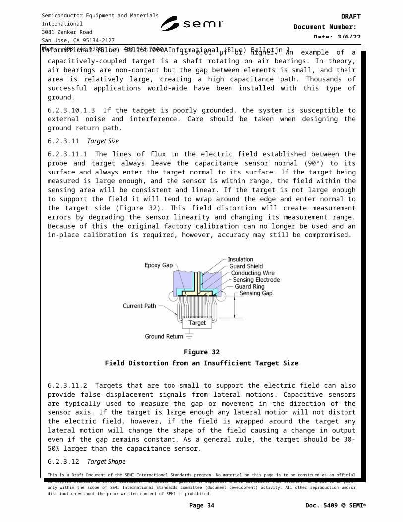
DRAFTDocument Number:
Date: 5/8/23
Figure 46Typical A-Scan Waveform Display (Left) and C-Scan Showing the Bond Quality at Several Layers of a Wafer
Bond StackNOTE: White and light gray areas indicate delamination present at several layers
6.4.5 Thickness Measurements with AM
6.4.5.1 As mentioned above, the A-Scan waveform consists of time and material interface data at an X-Y location on a bonded wafer. Knowing the speed of sound within a material converts the time data to a distance between one material interface and another, as shown in Figure 47 on the left. The time/distance data can be processed to color code the defects at different layers, as shown in Figure 47 on the right.
Figure 47An Example of a Color Coded Profile Image That Maps the Distance from the Surface of a Part to Anomalies
at a Specific Depth Within a Stacked WaferNOTE: All anomalies of the same color are at the same depth and the color map indicates that the blue anomalies are closer to the
top surface, deeper green and orange being the deepest in the stack.
6.4.5.2 In addition, thickness measurement of a layer within a wafer stack can be obtained, as shown in Figure 48. In this image, the C-scan image is shown on the left, while the A-Scan waveforms showing the full bonded wafer thickness, the delamination region, and defective regions within the stack are shown on the right. The data shown in Table 1 shows the time and distance measurements, based on the speed of sound of the material, made on a sample at five points of interest.
This is a Draft Document of the SEMI International Standards program. No material on this page is to be construed as an official or adopted Standard or Safety Guideline. Permission is granted to reproduce and/or distribute this document, in whole or in part, only within the scope of SEMI International Standards committee (document development) activity. All other reproduction and/or distribution without the prior written consent of SEMI is prohibited.
Page 34 Doc. jn l SEMI
Semiconductor Equipment and Materials International3081 Zanker RoadSan Jose, CA 95134-2127Phone: 408.943.6900, Fax: 408.943.7943

DRAFTDocument Number:
Date: 5/8/23
Figure 48C-Scan Image of a Stacked Wafer Showing 3 A-Scan Waveforms
NOTE: Waveform #1 shows the complete thickness of the stacked wafer. Waveforms #2 and #3 show the distance from the top surface to the delamination and anomalous regions within the wafer stack.
Table 1 Example Table of Various Thicknesses Measured at 5 Positions on a Sample.Waveform Thickness (ns) Thickness (m)
1 87 1082 81 1013 60 754 70 875 69 86
6.4.6 Bonded Wafer Thickness, TTV, Warp, Bow, Sori, and Flatness Metrology with Acoustic Microscopy (AM)
6.4.6.1 Acoustic microscopy (AM) collects data similar to a depth finder in that it can measure the transit time for sound from a reference point, in this case the transducer, to the first surface it sees. The contour of that surface over the X-Y area scanned can then easily be displayed in a simple color coded map or process further to provide specific warp, bow, sori or global flatness data. In Figures 49 and 50, examples are provided of both types of data displays for 3D measurement of wafer stack surface contours.
This is a Draft Document of the SEMI International Standards program. No material on this page is to be construed as an official or adopted Standard or Safety Guideline. Permission is granted to reproduce and/or distribute this document, in whole or in part, only within the scope of SEMI International Standards committee (document development) activity. All other reproduction and/or distribution without the prior written consent of SEMI is prohibited.
Page 35 Doc. jn l SEMI
Semiconductor Equipment and Materials International3081 Zanker RoadSan Jose, CA 95134-2127Phone: 408.943.6900, Fax: 408.943.7943

DRAFTDocument Number:
Date: 5/8/23
Figure 49Example of an AM Surface Flatness Color-Coded Display with Data Overlaid
NOTE: In this case the wafer stack is bowed 140 μm from center to edge.
Figure 50Example of a 3D AM Surface Flatness Map with the Data Processed and Displayed.
This is a Draft Document of the SEMI International Standards program. No material on this page is to be construed as an official or adopted Standard or Safety Guideline. Permission is granted to reproduce and/or distribute this document, in whole or in part, only within the scope of SEMI International Standards committee (document development) activity. All other reproduction and/or distribution without the prior written consent of SEMI is prohibited.
Page 36 Doc. jn l SEMI
Semiconductor Equipment and Materials International3081 Zanker RoadSan Jose, CA 95134-2127Phone: 408.943.6900, Fax: 408.943.7943

DRAFTDocument Number:
Date: 5/8/23
6.4.6.1.1 A summary of the techniques described in this guide is shown in Table 2 showing whether they are a high-volume manufacturing tool, and whether they measure the thickness of the wafer stack or the individual wafer components. The content is based on supplier information and is subject to change.
Table 2 Summary of Techniques in Guide
Metrology Technique HVMNon-HVM
Measurements Made
Capable of Measuring
Each Wafer in Bonded Wafer
Pair
Capable of Measuring Bond
Layer
White Light Confocal Microscope
Y YThickness, TTV,
Bow, WarpN N
IR Laser Profiling Y YThickness, TTV,
Bow, WarpY Y
White Light Interferometry
Y YThickness, TTV,
Bow, WarpN N
Infrared Interferometry/Confocal
MicroscopeY Y
Thickness, TTV, Bow, Warp
Y Y
Capacitance Metrology Y YThickness, TTV,
Bow, WarpN N
Differential Backpressure Metrology
Y YThickness, TTV,
Bow, WarpN N
Acoustic Microscopy Y YThickness, TTV,
Bow, WarpY Y
NOTICE: Semiconductor Equipment and Materials International (SEMI) makes no warranties or representations as to the suitability of the Standards and Safety Guidelines set forth herein for any particular application. The determination of the suitability of the Standard or Safety Guideline is solely the responsibility of the user. Users are cautioned to refer to manufacturer’s instructions, product labels, product data sheets, and other relevant literature, respecting any materials or equipment mentioned herein. Standards and Safety Guidelines are subject to change without notice.
By publication of this Standard or Safety Guideline, SEMI takes no position respecting the validity of any patent rights or copyrights asserted in connection with any items mentioned in this Standard or Safety Guideline. Users of this Standard or Safety Guideline are expressly advised that determination of any such patent rights or copyrights, and the risk of infringement of such rights are entirely their own responsibility.
This is a Draft Document of the SEMI International Standards program. No material on this page is to be construed as an official or adopted Standard or Safety Guideline. Permission is granted to reproduce and/or distribute this document, in whole or in part, only within the scope of SEMI International Standards committee (document development) activity. All other reproduction and/or distribution without the prior written consent of SEMI is prohibited.
Page 37 Doc. jn l SEMI
Semiconductor Equipment and Materials International3081 Zanker RoadSan Jose, CA 95134-2127Phone: 408.943.6900, Fax: 408.943.7943