figure 10.1. a flip-flop with an enable input. d q q q r clock e 0 1
TRANSCRIPT

Figure 10.1. A flip-flop with an enable input.
D Q
Q
Q R
Clock
E
0 1

Figure 10.2. Code for a D flip-flop with enable.
module rege (R, Clock, Resetn, E, Q);input R, Clock, Resetn, E;output Q;reg Q;
always @(posedge Clock or negedge Resetn)
if (Resetn == 0)Q <= 0;
else if (E)Q <= R;
endmodule

Figure 10.3. An n-bit register with an enable input.
module regne (R, Clock, Resetn, E, Q);parameter n = 8;input [n-1:0] R;input Clock, Resetn, E;output [n-1:0] Q;reg [n-1:0] Q;
always @(posedge Clock or negedge Resetn)
if (Resetn == 0)Q <= 0;
else if (E)Q <= R;
endmodule

Figure 10.4. A shift register with parallel-load and enable control inputs.

Figure 10.5. A right-to-left shift register with an enable input.
module shiftlne (R, L, E, w, Clock, Q);parameter n = 4;input [n-1:0] R;input L, E, w, Clock;output [n-1:0] Q;reg [n-1:0] Q;integer k;
always @(posedge Clock)begin if (L)
Q <= R;else if (E)begin
Q[0] <= w;for (k = 1; k < n; k = k+1)
Q[k] <= Q[k-1];end
end
endmodule

Figure 10.6. An SRAM cell.
Sel
DataData

Figure 10.7. A 2 x 2 array of SRAM cells.
Sel 1
Sel 0
Data0 Data1

Figure 10.8. A 2m x n SRAM block.
Sel 2
Sel 1
Sel 0
Sel 2 m 1 ”
Read
Write
d 0 d n 1 – d n 2 –
q 0 q n 1 – q n 2 –
m -to-2
m deco
der
Address
a 0
a 1
a m 1 –
Data outputs
Data inputs

Figure 10.9. Pseudo-code for the bit counter.
B = 0 ; while A 0 do
if a 0 = 1 thenB = B + 1 ;
end if;Right-shift A ;
end while;

Figure 10.10. ASM chart for the pseudo-code in Figure 10.9.
Please see “portrait orientation” PowerPoint file for Chapter 10

Figure 10.11. Datapath for the ASM chart in Figure 10.10.
L
E Counter
w
L
E Shift
LB
EBLA
EA
0
Clock
0
B z a 0
Data
n
A
n
(log2 n) + 1
(log2 n) + 1

Figure 10.12. ASM chart for the bit counter datapath circuit.
EA
EB z
LB
s
a 0
Reset
S3
0
1
0
1
0
1 s
S2
S1
0
1
Done
Figure 10.13. Verilog code for the bit-counting circuit.
Please see “portrait orientation” PowerPoint file for Chapter 10

Figure 10.14. Simulation results for the bit-counting circuit.

Figure 10.15. An algorithm for multiplication.
(a) Manual method
P = 0 ; for i = 0 to n 1 do
if b i = 1 thenP = P + A ;
end if; Left-shift A ;
end for;
(b) Pseudo-code
Multiplicand11
Product
Multiplier10
01
11
11011011
00001011
01 001111
Binary
1311
1313
143
Decimal
–

Figure 10.16. ASM chart for the multiplier.
Please see “portrait orientation” PowerPoint file for Chapter 10

Figure 10.17. Datapath circuit for the multiplier.
Please see “portrait orientation” PowerPoint file for Chapter 10

Figure 10.18. ASM chart for the multiplier control circuit.
Please see “portrait orientation” PowerPoint file for Chapter 10

Figure 10.19. Verilog code for the multiplier circuit.
Please see “portrait orientation” PowerPoint file for Chapter 10

Figure 10.20. Simulation results for the multiplier circuit.

Figure 10.21. An algorithm for division.
R = 0 ; for i = 0 to n 1 do
Left-shift R A ; if R B then
q i = 1 ; R = R B ;
elseq i = 0 ;
end if; end for;
(c) Pseudo-code
9 14095045
5
15
100
1010
011001001
00001111
100100101
10000100111101001101
Q
AB
R(a) An example using decimal numbers
(b) Using binary numbers
–
–

Figure 10.22. ASM chart for the divider.
Please see “portrait orientation” PowerPoint file for Chapter 10

Figure 10.23. Datapath circuit for the divider.
E L
E
L
E
DataB
LR
ER
EQ
Clock
Q
Register
EB
0
R
DataA LA
EA
+ E c out c in 1
B
w
Rsel
n
Left-shiftregister
n
Left-shiftregister
n n
n n
n n
Left-shiftregister
a n 1 ” A
w
0 1

Figure 10.24. ASM chart for the divider control circuit.
Please see “portrait orientation” PowerPoint file for Chapter 10

Figure 10.25. An example of division using n = 8 clock cycles.
Load A, B 0 0 0 1
0 0 1 1
0 1 2 3 1
0 0
0 0 0
4 5 6 0 0 7
1 0 0 0 1 1 0 0
Clock cycle
0 0 8
0
A/Q
0 1 1 0
1 1 0 0
0 0 0
0 0 0
0 0 0 0
1 0 0 0
0 0 0 0
0 0 0
0 0 0
0 1 1 1
0 0 0 0 0 0 1 1 1
0 0 0 0 1 1 1 1
rr0 R
0 0 0 0
0 0 0 0
0 0 0
0 0 0
0 0
0 0 0 0 0 0 0 0
0 0 0
0 0 0 0
0 0 0 0
0 1 1
1 0 0
1 0 0 1
0 0 0 1
0 0 1 0
0 0 0
0 0 0
0 0 1 1
0 1 0 0 0 1 1 0 0
0 0 0 0 1 0 1 0
0 0 0 0 0 0 0 0 0 0
100011001001 A B
Shift left
Subtract, Q 0 1
Shift left, Q 0 0 Shift left, Q 0 0 Shift left, Q 0 0
Subtract, Q 0 1 Subtract, Q 0 1 Subtract, Q 0 1
Shift left, Q 0 0

Figure 10.26. ASM chart for the enhanced divider control circuit.
Please see “portrait orientation” PowerPoint file for Chapter 10

Figure 10.27. Datapath circuit for the enhanced divider.
Please see “portrait orientation” PowerPoint file for Chapter 10

Figure 10.28. Verilog code for the divider circuit.
Please see “portrait orientation” PowerPoint file for Chapter 10
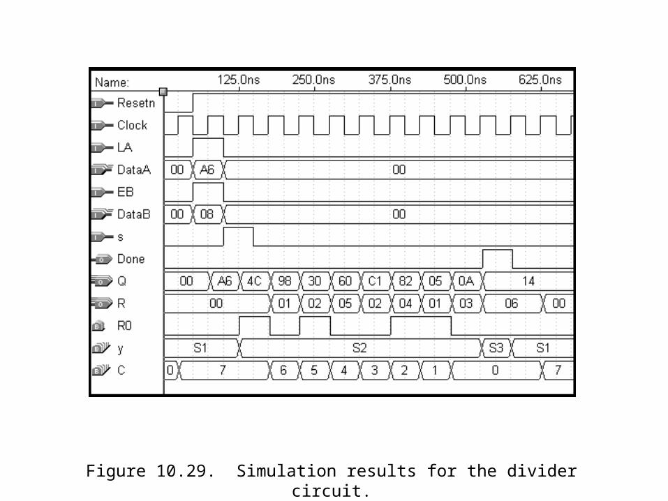
Figure 10.29. Simulation results for the divider circuit.

Figure 10.30. An algorithm for finding the mean of k numbers.
Please see “portrait orientation” PowerPoint file for Chapter 10

Figure 10.31. Datapath circuit for the mean operation.
Please see “portrait orientation” PowerPoint file for Chapter 10

Figure 10.32. ASM chart for the mean operation control circuit.
Please see “portrait orientation” PowerPoint file for Chapter 10
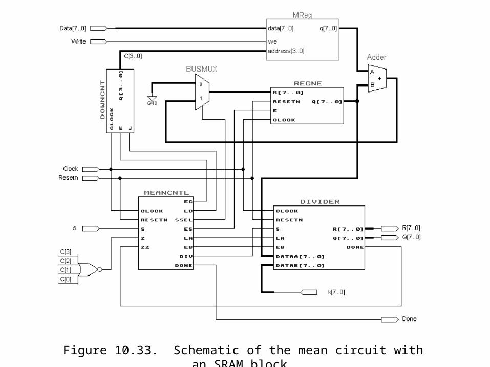
Figure 10.33. Schematic of the mean circuit with an SRAM block.

Figure 10.34. Simulation results for the mean circuit using SRAM.
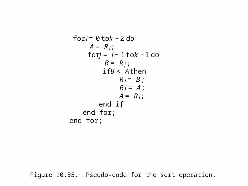
Figure 10.35. Pseudo-code for the sort operation.
for i = 0 to k 2 doA = R i ; for j = i + 1 to k 1 do
B = R j ; if B < A then
R i = B ; R j = A ; A = R i ;
end if ; end for;
end for;
–
–

Figure 10.36. ASM chart for the sort operation.
Please see “portrait orientation” PowerPoint file for Chapter 10

Figure 10.37. A part of the datapath circuit for the sort operation.
E E E E
Clock
DataIn
WrInit
Rin 3 Rin 2 Rin 1 Rin 0
E E Bin Ain
DataOut
Rd
ABData
Imux
Bout
BltA
1 0 A B
0 1
RData
R 0 R 1 R 2 R 3
0 1 2 3
ABmux n
n
n

Figure 10.38. A part of the datapath circuit for the sort operation.
L
E
L
E
1 0
1 0
k 2 ” =
k 1 ” =
LJ
EJ
LI
EI
2-to-4 decoder
WrInit
Wr
RAdd
Clock
Csel
Int
Imux
2
C i C j
z i
z j Cmux
Rin 0
Rin 1
Rin 2
Rin 3
0
2
2
2
2
2
Counter Counter
R
Q Q
R
w 0 w 1
En
y 0
y 1
y 2
y 3
2

Figure 10.39. ASM chart for the control circuit.
Please see “portrait orientation” PowerPoint file for Chapter 10

Figure 10.40. Verilog code for the sorting circuit.
Please see “portrait orientation” PowerPoint file for Chapter 10
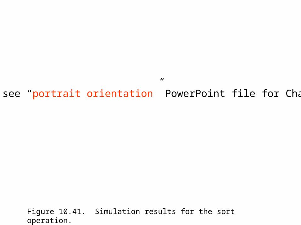
Figure 10.41. Simulation results for the sort operation.
Please see “portrait orientation” PowerPoint file for Chapter 10

Figure 10.42. Using tri-state buffers in the datapath circuit.
E E E E
Clock
DataIn
WrInit
Rin 3 Rin 2 Rin 1 Rin 0
E E Bin Ain
A B
BltABout
Aout
DataOut
Rd
Rout3 Rout2 Rout1 Rout0
n
n
n n n n
n
n n
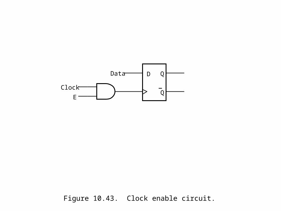
Figure 10.43. Clock enable circuit.
D Q
Q
Data
Clock
E

Figure 10.44. An H tree clock distribution network.
Clock
ff
ff
ff
ff
ff
ff
ff
ff
ff
ff
ff
ff
ff
ff
ff
ff

Figure 10.45. A flip-flop in an integrated circuit.
D Q
Data
Clock
Chip package pin
A
B
t Clock
t Data
Out
t od

Figure 10.46. Flip-flop timing in a chip.
Data
Clock
A
3ns
4.5ns
1.5ns
B

Figure 10.47. Asynchronous inputs.
D Q
Q
Data
Clock
(asynchronous)D Q
Q
Data(synchronous)

Figure 10.48. Switch debouncing circuit.
Data
S
R
V DD
R
V DD
R
(a) Single-pole single-throw switch
Data
V DD
R
(b) Single-pole double-throw switch with a basic SR latch

Figure P10.1. Pseudo-code for integer division.
Q = 0 ; R = A ; while ((R B) > 0) do
R = R B ; Q = Q + 1 ;
end while ;
––

Figure P10.2. The 555 programmable timer chip.
5 V
R b
R a
555 Timer
8
7
6
5 1
2
3
4
C 1
0.01F
Clock (output)