ferromagnetic semiconductors for spintronics kevin edmonds, kaiyou wang, richard campion, devin...
TRANSCRIPT
Ferromagnetic semiconductors for spintronics
Kevin Edmonds, Kaiyou Wang, Richard Campion, Devin Giddings, Nicola Farley, Tom Foxon, Bryan Gallagher, Tomas JungwirthSchool of Physics & Astronomy, University of Nottingham
Mike Sawicki, Tomasz DietlIFPAN, Warsaw, Poland
Tarnjit Johal, Gerrit van der LaanDaresbury Laboratory
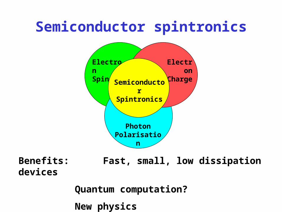
ElectronCharge
Photon Polarisation
ElectronSpin
Semiconductor Spintronics
Semiconductor spintronics
Benefits: Fast, small, low dissipation devices
Quantum computation?
New physics
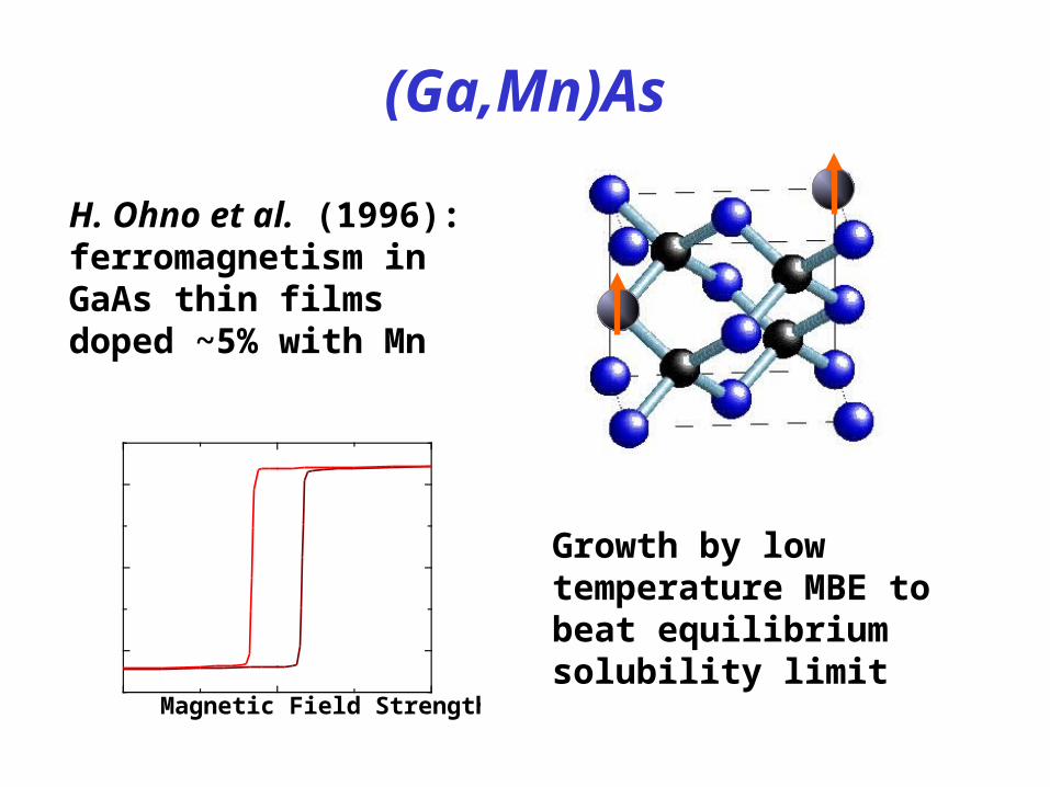
(Ga,Mn)As
H. Ohno et al. (1996): ferromagnetism in GaAs thin films doped ~5% with Mn
Magnetic Polarisation
Magnetic Field Strength
Growth by low temperature MBE to beat equilibrium solubility limit
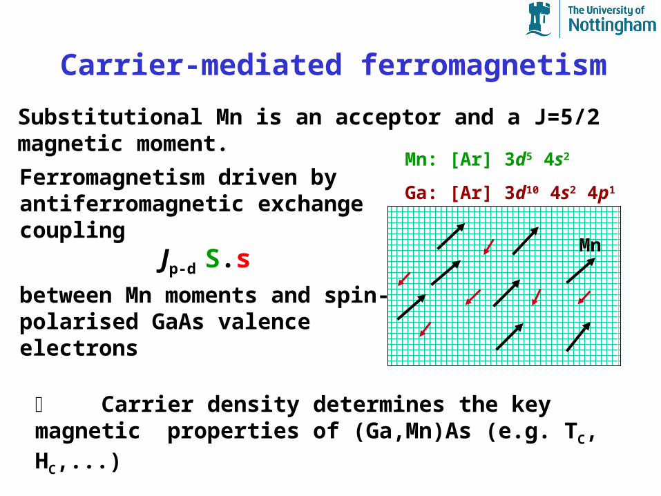
Carrier-mediated ferromagnetism
Substitutional Mn is an acceptor and a J=5/2 magnetic moment.
Ferromagnetism driven by antiferromagnetic exchange coupling
Jp-d S.sbetween Mn moments and spin-polarised GaAs valence electrons
Carrier density determines the key magnetic properties of (Ga,Mn)As (e.g. TC, HC,...)
Mn: [Ar] 3d5 4s2
Ga: [Ar] 3d10 4s2 4p1
Mn

Carrier-mediated ferromagnetism
Spin-FETH. Ohno et al., Nature (2000)
Vgate
InMnAs
Photogenerated magnetism Koshihara PRL (1997)
InMnAs
GaSb
B (mT)
ħ
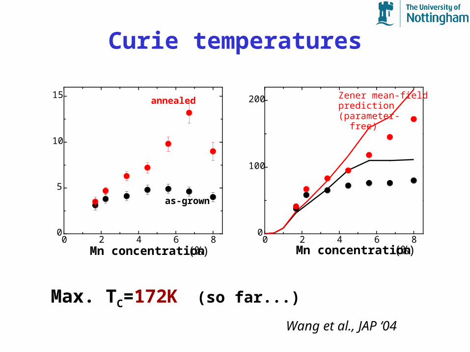
Curie temperatures
0 2 4 6 80
100
200 Zener mean-fieldprediction(parameter- free)
Curie temp.
(K)
Mn concentration (%)0 2 4 6 8
0
5
10
15
as-grown
annealed
Carrier density
(x10
20
/cc)
Mn concentration (%)
Max. TC=172K (so far...)
Wang et al., JAP ‘04

Interstitial Mn: a magnetism killer
Yu et al., PRB ’02: ~10-20% of total Mn concentration is incorporated as interstitials
Increased TC on annealing corresponds to removal of these defects.
Mn
As
Negative effects on magnetic order:
compensating donor – reduces hole density
antiferromagnetic coupling between interstitial and substitutional Mn predicted Blinowski PRB ‘03
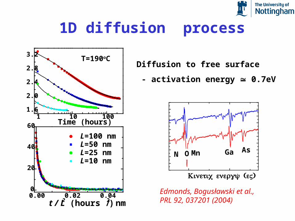
1 10 1001.6
2.0
2.4
2.8
3.2
0.00 0.02 0.040
20
40
60
t / L2 (hours / nm2) d(1/ρ)/dt (mΩ-1 cm
-1 hours
-1)
Resistivity (m
Ω cm)
Time (hours)
L=100 nm L=50 nm L=25 nm L=10 nm
AsGaMnON
dΦ / dE
( )Kinetic energy eV
1D diffusion process
Diffusion to free surface
- activation energy 0.7eV
Edmonds, Bogusławski et al., PRL 92, 037201 (2004)
T=190oC
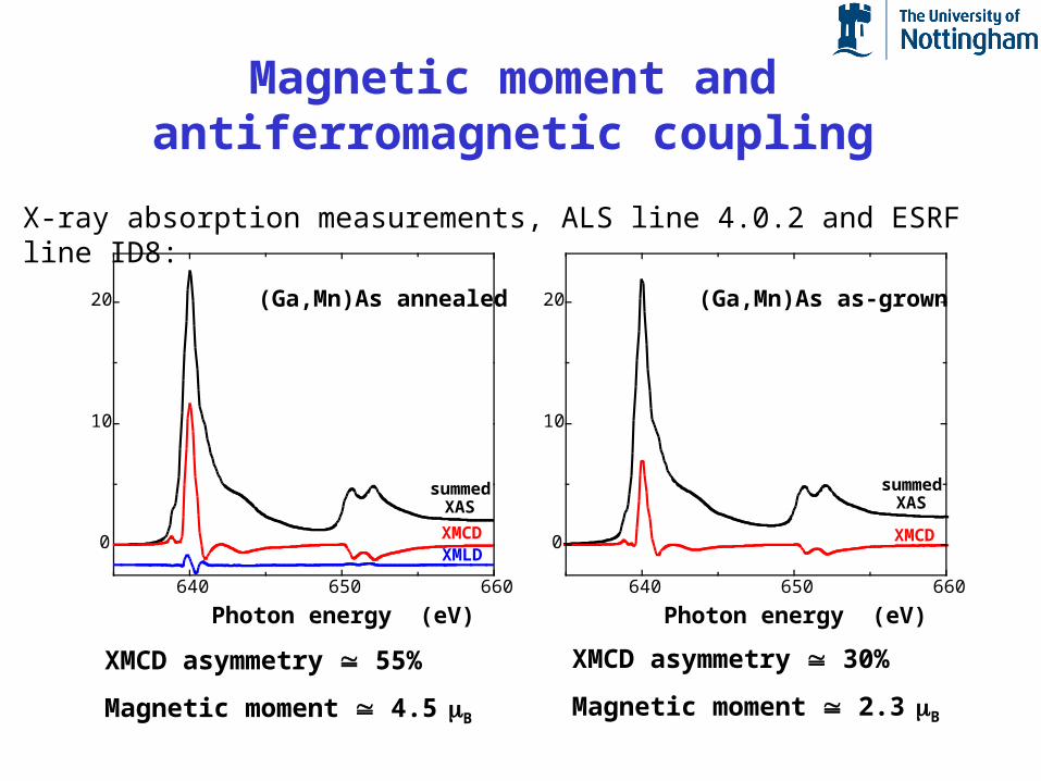
Magnetic moment and antiferromagnetic coupling
XMCD asymmetry 55%
Magnetic moment 4.5
B
640 650 660
0
10
20
summedXAS
(Ga,Mn)As as-grown(Ga,Mn)As annealed
summedXAS
XMLDXMCD
absorption (a.u.)
Photon energy (eV)640 650 660
0
10
20
XMCD
Photon energy (eV)
XMCD asymmetry 30%
Magnetic moment 2.3
B
X-ray absorption measurements, ALS line 4.0.2 and ESRF line ID8:
640 650
X-ray energy (eV)
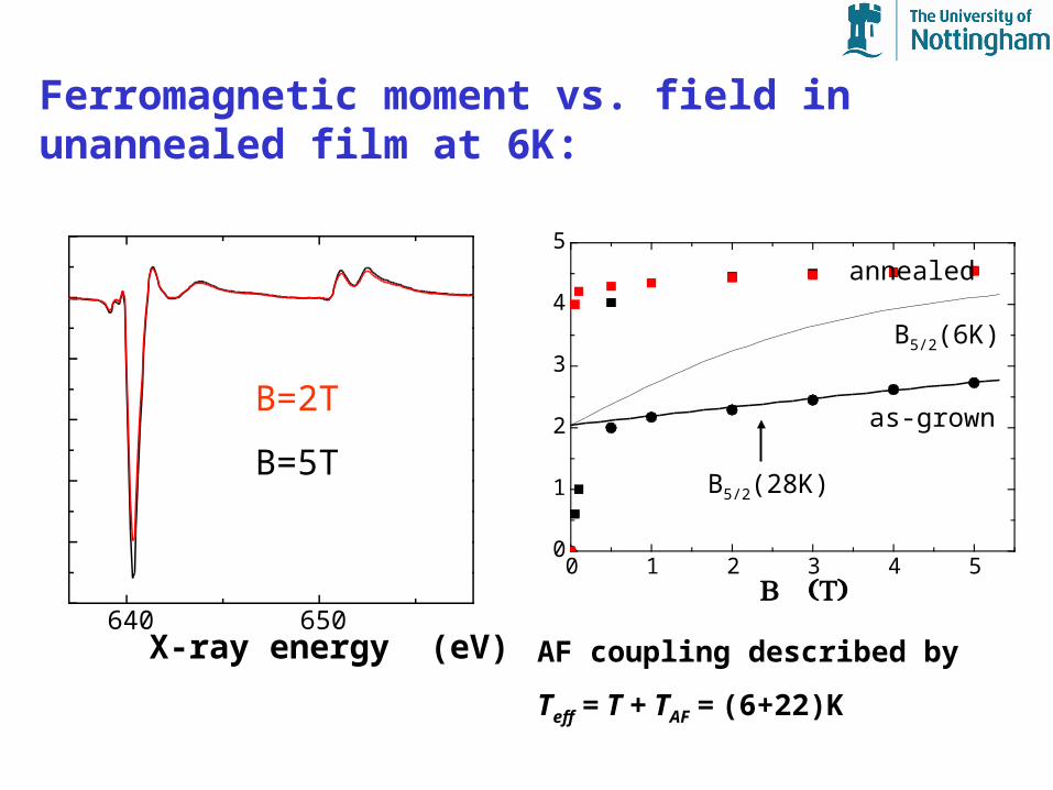
0 1 2 3 4 50
1
2
3
4
5
S+l (B/ )Mn
( )B T
B=2T
B=5T
annealed
as-grown
B5/2(6K)
B5/2(28K)
Ferromagnetic moment vs. field in unannealed film at 6K:
AF coupling described by
Teff = T + TAF = (6+22)K
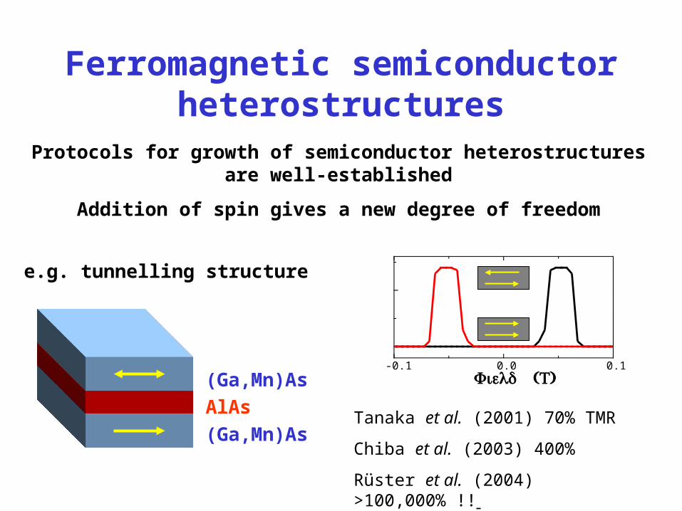
Ferromagnetic semiconductor heterostructures
Protocols for growth of semiconductor heterostructures are well-established
Addition of spin gives a new degree of freedom
e.g. tunnelling structure
(Ga,Mn)AsAlAs(Ga,Mn)As
Tanaka et al. (2001) 70% TMR
Chiba et al. (2003) 400%
Rüster et al. (2004) >100,000% !!
-0.1 0.0 0.1
R (ΜΩ)
( )Field T
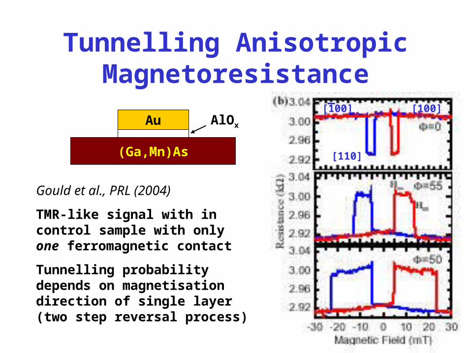
Tunnelling Anisotropic Magnetoresistance
(Ga,Mn)As
Au AlOx
Gould et al., PRL (2004)
TMR-like signal with in control sample with only one ferromagnetic contact
Tunnelling probability depends on magnetisation direction of single layer (two step reversal process)
[110]
[100] [100]

0 5 10
0
4
8
exper. AMR⊥ . exper AMR// theory AMR⊥ theory AMR//
(-%)AMR
(%)Mn
I M
Anisotropic magnetoresistance
Magnetoresistance on rotating M away from ‘x’ direction
- strong function of Mn concentration, well described by mean-field model
Jungwirth et al. APL ‘03-0.5 0.0 0.5
315
320
R (Ω)
( )B T

10K 4.2K 1.5K
V [mV]
I [nA]
TAMR in Nanoconstrictions
5nm (Ga,Mn)As film with 30nm wide constrictions
Giant anisotropic magnetoresistance ~100% in tunnelling regime
Giddings et al., cond-mat/0409209
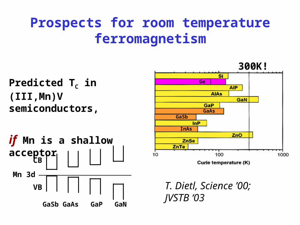
Prospects for room temperature ferromagnetism
GaAs
InAs
GaSb
Ge
300K!
T. Dietl, Science ’00; JVSTB ‘03
GaSb GaAs GaP GaN
CB
VB
Mn 3d
Predicted TC in (III,Mn)V semiconductors,
if Mn is a shallow acceptor
-50 -40 -30 -20 -10 0-5
-4
-3
-2
-1
0
1Ga
1-xMn
xN x=0.3%
M (emu/cm
3)
H (kOe)
T = 400 K T = 10 K T = 8 K T = 6 K T = 4 K
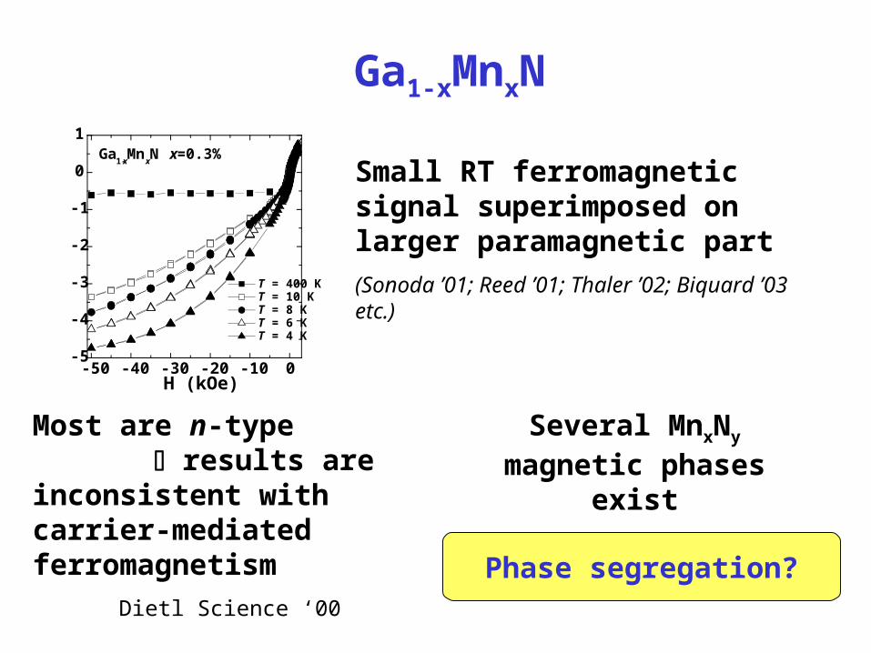
Ga1-xMnxN
Small RT ferromagnetic signal superimposed on larger paramagnetic part(Sonoda ’01; Reed ’01; Thaler ’02; Biquard ’03 etc.)
Several MnxNy magnetic phases
existZajac et al. ‘03
Most are n-type results are
inconsistent with carrier-mediated ferromagnetism
Dietl Science ‘00
Phase segregation?
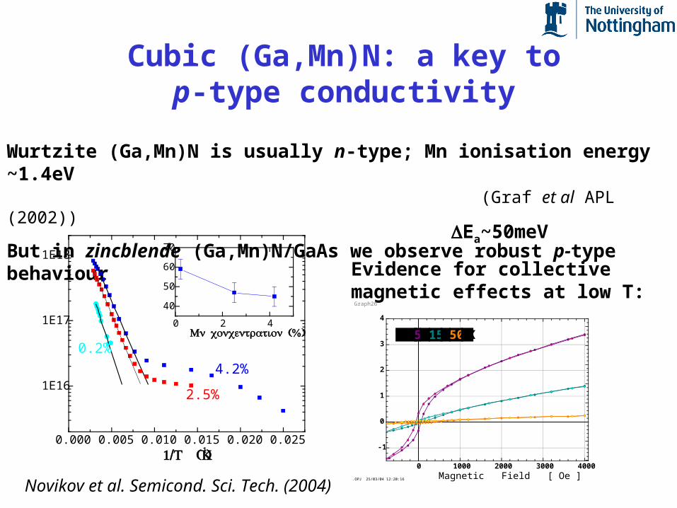
Cubic (Ga,Mn)N: a key to p-type conductivity
Wurtzite (Ga,Mn)N is usually n-type; Mn ionisation energy ~1.4eV(Graf et al APL (2002))
But in zincblende (Ga,Mn)N/GaAs we observe robust p-type behaviour
0.000 0.005 0.010 0.015 0.020 0.025
1E16
1E17
1E18
0 2 4
40
50
60
70
0.2%
2.5%
4.2%
ΔEa ( )meV
(%)Mn concentration
pHall
(cm
-3)
1/ (T K-1)
ΔEa~50meV
Evidence for collective magnetic effects at low T:
0 1000 2000 3000 4000
-1
0
1
2
3
4
T = 5 / 15 / 50 K
.OPJ 25/03/04 12:20:16
Graph26
Moment [ emu/cm
3 ]
Magnetic Field [ Oe ]
Novikov et al. Semicond. Sci. Tech. (2004)
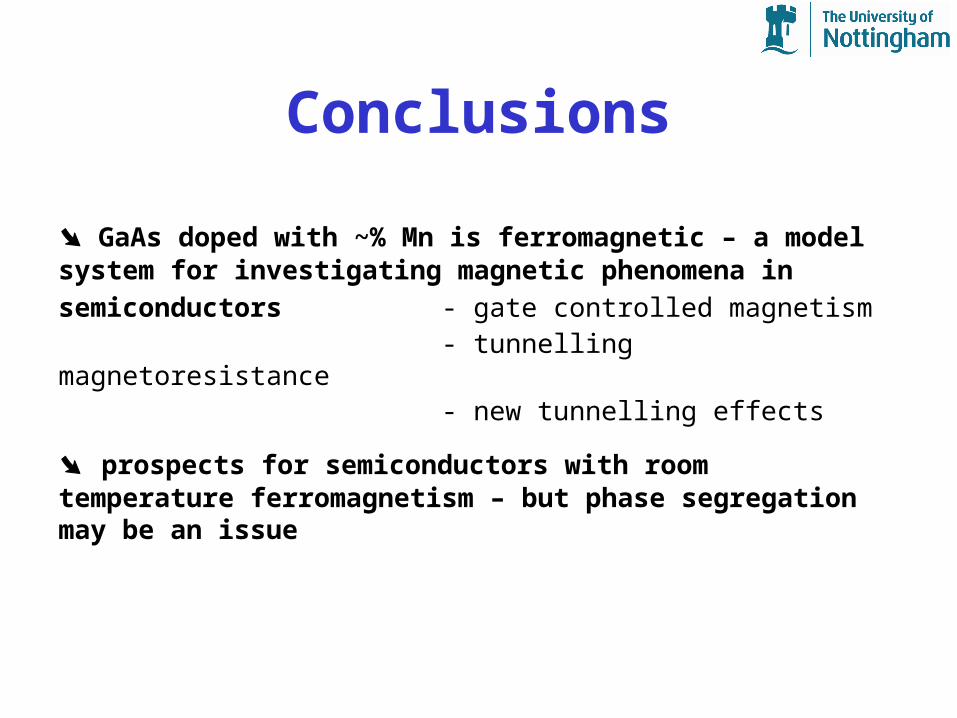
Conclusions
GaAs doped with ~% Mn is ferromagnetic – a model system for investigating magnetic phenomena in semiconductors - gate controlled magnetism
- tunnelling magnetoresistance- new tunnelling effects
prospects for semiconductors with room temperature ferromagnetism – but phase segregation may be an issue
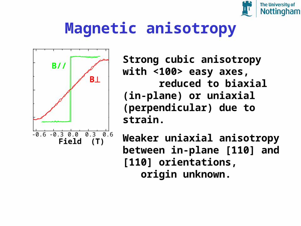
Magnetic anisotropy
-0.6 -0.3 0.0 0.3 0.6
Magnetisation (a.u.)
Field (T)
Strong cubic anisotropy with <100> easy axes,
reduced to biaxial (in-plane) or uniaxial (perpendicular) due to strain.
Weaker uniaxial anisotropy between in-plane [110] and [110] orientations, origin unknown.
B
B//
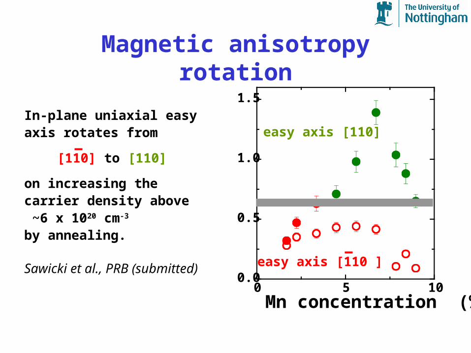
Magnetic anisotropy rotation
0 5 100.0
0.5
1.0
1.5
Carrier density (nm
-3)
Mn concentration (%)
easy axis [110]
easy axis [110 ]
In-plane uniaxial easy axis rotates from
[110] to [110]
on increasing the carrier density above ~6 x 1020 cm-3 by annealing.
Sawicki et al., PRB
(submitted)