ferroelectric thin films for integrated passive components … bound... · ferroelectric thinfilms...
TRANSCRIPT
Philips Journal of Research Vol. SI No.3 1998 363
Philips J. Res. 51 (1998) 363-387
FERROELECTRIC THIN FILMS FOR INTEGRATEDPASSIVE COMPONENTS
by M. KLEE, U. MACKENS, R. KIEWITT, G. GREUELand C. METZMACHER
Philips GmbH Forschungslaboratorien, Aachen, Germany
AbstractMiniaturisation and integration of passive components play an importantrole in today's components market. It can be achieved by applying thin-filmtechnologies for capacitors, resistors and inductors; high componentdensities have been realised with 'Passive Only Networks'. The dielectricmaterials used for integrated thin-film capacitors ranging from Si3N4,
Ta20s, Ti02 to earth alkaline as well as lead perovskite layers arereviewed. The capacitor performances including temperature stability,insulation resistance, breakdown fields and endurance are discussed as afunction of material composition.
1. Introduetion
1.1. Miniaturisation of passive components
The miniaturisation of electronic systems, especially those found in hand-held and portable systems and the higher clock frequencies in ElectronicData Processing Systems, raise the demand for miniaturised electronic com-ponents and increased functionality. Miniaturisation of electronic circuitsthus goes along with an increase in the functionality of the active componentsand a large size reduction ofpassive components. The size reduction ofpassivecomponents plays a role in analogue/digital circuits in particular where thepassive components can make up to 70% of the components in thecircuitry. Miniaturisation of passive components is, therefore, besides costreduction and improvement of quality, a major issue in today's passive com-ponents market.
Passive components such as ceramic multilayer capacitors (CMCs) andresistors are, therefore, continuously reduced in size. Lateral dimensions

M. Klee et al.
down to 0.5mnr' are standard (so-called 0402 products) and for specialproducts, lateral dimension down to 0.I25mm2 are available on the market(so-called 0201 products).
Continuous miniaturisation of discrete components down to lateral dimen-sions of 0.125mm2 demands highly sophisticated processing technologies aswell as improved mounting, placing and soldering processes. Integration ofpassive components is the way to overcome these problems.
1.2. Integration of passive components
1.2.1. Ceramicprocessing
Several passive components manufacturers [1,2] have developed ceramicprocesses to integrate passive components into ceramic modules. Low-temperature co-firing techniques for dielectric materials and ferromagneticmaterials result in ceramic modules composed of capacitors and inductors.Numerous types of ceramic modules are offered to customers for applicationssuch as filtering [1,2]. Complex ceramic modules are also fabricated using thesemultilayer techniques. Highly sophisticated materials and sintering techniquesare developed, which enable large and small capacitors to be produced in onemodule. Various types ofmaterials are applied and barriers layers are used toprevent reactions and interdiffusions. On top of the modules, resistors areprinted together with footprints for mounting of packaged ICs [2].
Low-firing technology is one method of co-sintering dielectric materialswith ferrites. Another method is the multilayer technique based on hotuniaxial processing. With this technique, a lowering of the sintering tempera-tures is achieved as 'well as precise control of the lateral dimensions duringsintering of the green, ceramic, multilayer products. Ceramic capacitornetworks and capacitor/resistor networks are described in more detail inRef. 1.
With ceramic modules, an increase of the component density up to 50-70components/cm'' is obtained, compared with discrete passive componentswhere a typical component density of 4-25 components/cmé is obtained.For further miniaturisation of electronic circuits, an increase of the compo-nent density can be achieved by switching from ceramic technology to athin-film process with high-density interconnects.
364 Phillips Journni of Research Vol. 51 No. 3 1998
1.2.2. Integrated passive components (IPCs) based on thin-film techniques
Thin-film process for capacitors, resistors and inductors offer passivefunctions with high component density (100-150 components/cm'') and high

Phillips Journal of Research Vol. 51 No. 3 1998 365
Ferroelectric thin films for integrated passive components
c R L
metal2
resistor '~=!!!===~I~~I~bIdielectric --~~;::' iimetal1
Fig. 1. Schematic drawing of one circuit type of integrated passive components.
precision (see Fig. 1). An attractive substrate is Si, due to its high surfacequality, high temperature stability and thermal expansion match with activefunctions.
Integrated passive components aim at capacitor networks, resistor networks andcapacitor-resistor-inductor networks for miniaturised, high performance electro-nic circuits in the electronic data processing (EDP) and telecommunicationmarkets. To be successfulin this new product area, an intensive development ofmaterials, processes, design and simulation is needed.
The design and simulation of circuits is described in Ref. [3].Discussions ontechnologies can be found in Ref. [4]. In this section, we will report on inves-tigations of dielectric materials for high-performance, thin-film capacitors.
1.2.3. Thin-film capacitors integrated into ICs
The highest density of components, combined with the hardest requirementson materials compatibility and processing, can be achieved by integratingpassive components directly into ICs. That passive components integratedinto ICs give rise to a significant miniaturisation of the circuit, as well as animprovement in performance of the device, has been demonstrated withmonolithic GaAs microwave ICs fabricated by Panasonic for mobile commu-nication devices [5]. To miniaturise the circuit, reduce costs and improveperformance, the external bypass capacitor of the circuit has been integratedinto the GaAs IC. To reduce the size of the approx. 800 pF capacitor, thinfilms based on Bal_xSrxTi03 are applied, which show relative permittivitiesa factor of 40 higher than Si3N4. Special features of these integratedcapacitors are the significant miniaturisation of the lateral dimensions of themonolayer capacitor and the operation up to 2 GHz without showing anydecrease of capacitance at these high frequencies.

M. Klee et al.
2. Dielectric materials for integrated passive components
2.1. Materials evaluation
Evaluation of materials and processes is one of the major issues in therealisation of IPCs. The major selection criteria are:
(1) The passive modules have to fulfil a number of specifications which aredefined by the application area of the system. (These specifications are,in most cases, related to discrete products.) Often special specificationshave to be achieved to improve the device performance.
(2) The selected materials have to be compatible with the overall thin-filmprocess.
(3) The material processes have to be low cost and compatible with a 'standardproduction' line.
In the following, thin-film dielectric materials and specifications for thin-filmcapacitor applications will be discussed. The evaluation of thin-film resistorswith respect to device performance has been reported in Ref. [6].
Dielectric materials that are compatible with Si substrates and with stan-dard process lines are Si02 and Si3N4. These dielectric materials show relativepermittivities of 5- 7 and breakdown fields of 8-10 MV [ctu, Standard deposi-tion processes for silicon oxide and silicon nitride as well as combinations ofsilicon oxide/nitride are low pressure chemical vapour deposition (LPCVD)and plasma enhanced chemical vapour deposition (PECVD). Planar capaci-tors are typically produced with capacitance densities of 50-500pF/mm2.The temperature dependence of the capacitance for these thin-film capacitorsis of the order of 20-40 ppm/K.For further extension of application range, capacitor and capacitor-resistor
networks, as well as capacitor-resistor-inductor networks, are of interestwith capacitance values above some hundred pF. To increase the capaci-tance range up to some tenths of a nF while keeping the capacitor areasmall, dielectric thin-film materials with a relative permittivity larger than7 are needed.Thin-film capacitors based on Ta20s dielectric layers, with a relative permit-
tivity of K = 21.5 and Ti02 with a relative permittivity of K = 85 show capa-citance densities of 1-8 nF/mm2. To produce thin-film capacitors with sometenths of a nF, ferroelectric thin-film materials have to be considered. Highrelative perrnittivities of K > 200 can be obtained with ferroelectric materialsbased on earth alkaline titanates or lead-based perovskites.Ferroelectric thin layers are well known in the electronics industry. They are
intensively studied for integrated devices such as non-volatile memories and
366 PhilUpsJournalof Research Vol. 51 No. 3 1998
Ferroelectric thin films for integrated passive components
high-density dynamic random accessmemories (see Ref. 7). The integration ofpassive components has until now, only reported by Noma [5].
2.2. Material performance for integrated thin-film capacitors
Integrated thin-film capacitors based on ferroelectric layers cover acapacitance range of some hundred pF up to several tenths of a nf'. Formost applications, the products have to operate at a maximum of 16V. Atypical temperature variation of these types of capacitors is ±10-15% in thetemperature range T = -55°C up to +125°C. The loss tangent at 25°C istypically specified as <3.5% at 1Vrms. The integrated capacitors have to behighly ohmic; the insulation resistance, measured at room temperature, hasto exceed 100 gigaohm. Modules operating at rated voltage have to withstandan applied de voltage of several times the rated voltage for 1 minute withoutdeterioration of the electrical performance.An important feature of the capacitor dielectrics is their endurance. Ceramic
capacitors based on ferroelectric materials show a degradation of the insula-tion resistance if a de voltage of rated voltage or several times the ratedvoltage is applied at elevated temperatures. The resistance degradation isdependent on the material composition, doping types and doping levels intro-duced in the ceramic. The resistance degradation of ferroelectric ceramics hasbeen intensively studied for doped SrTi03 ceramics as well as single crystalsand is caused by diffusion of oxygen vacancies in the electrical field [8].Although intensive studies have been carried out for bulk ceramics, only fewdata are known for ferroelectric thin-films. For integrated thin-film capaci-tors, the resistance degradation under a dc field is essential. Thin films of sub-micron thickness have to operate at voltages of up to 16V, which correspondswith electrical fields of E = 100-400 kV[es», These are extremely high operat-ing fields compared with standard ceramic capacitors where operating fields of10-30 kVlcm are typical.Another feature of ferroelectric capacitors is their ageing performance.
Ageing of ceramic capacitors is well known. The effect is a spontaneous andgradual decrease in dielectric constant as time passes. The decrease follows alogarithmic time law. The magnitude of decrease in dielectric constant,expressed in percentage per decade of time, is called the ageing rate. Ageingof ceramics has been intensively studied by several groups especially forBaTi03 with acceptor dopants. For ceramic multilayer capacitors based onBaTi03, ageing rates of the order of 0.8-8% are typical. Arlt and Robelsdeveloped a model which supposes that internal electrical fields, formedfrom dipoles of oxygen vacancies and acceptors, pin domain walls and thus
Phillips Journnl of Research Vol. SI No.3 1998 367

M. Klee et al.
give rise to the ageing ofthe ferroelectric ceramic capacitors [9]. In the case ofthe more complex relaxor ferroelectrics, such as Pb(Mg1/3Nb2/3)03' Schrout[10] reported a working model for ageing in relaxor ferroelectrics and Haradaet al. [11]published ageing rates for CMCs with PLZT ceramics of -2% andfor CMCs based on relaxors of -8%.
The ageing performance of thin ferroelectric BaTi03, SrTi03 or relaxorthin-film capacitors has not yet been reported. The first ageing results onour ferroelectric thin-film capacitors will be discussed in Sec. 4.3.
2.3. Thin-film pocesses for ferroelectric layers
In the last 5-10 years, numerous ferroelectric thin-films processes have beendeveloped, especially for non-volatile memories and high-density dynamicrandom access memories. The most intensively studied techniques for com-plex oxidic thin layers such as ferroelectric films are wet-chemical pro-cesses. Solutions containing metal alkoxides, in the case of the sol-gelprocesses and in the case of metallo-organic decomposition processes(MOD) metallo-organic compounds such as metal carboxylates dissolvedin organic solvent such as alcohols [12,13] are deposited on substratesby spin-coating, dip-coating and spray-coating. The solvents are evapo-rated during heating, the metal alkoxides are polymerised and the metalcarboxylates are decomposed. At temperatures of 500-700 DC, the filmsare crystallised into the ferroelectric phase. Also the so-called liquidsource CVD process [14], which is especially developed for non-volatilememories with layered perovskite dielectrics such as SrBi2Ta206, is atype of wet-chemical process. Solutions containing precursors such as Sr,Bi carboxylates and Ta ethoxide dissolved in alcohols are nebulized andtransported with a carrier gas such as N2 to the substrate surface. Afterfilm deposition, heat treatment processes take place similar to spin-coatingor dip-coating techniques.
All these wet-chemical processing techniques are attractive for ternary andquaternary oxidic layers. Precise compositional control ofthe layers, flexibilityof the processing and compatibility with standard Si technology are specialfeatures of these techniques. Another attractive feature of the wet-chemicalprocessing techniques is their low investment cost.
For applications such as non-volatile memories or high-density dynamicrandom access memories, capacitor layouts with high densities and thus agood step-coverage are needed. For these applications especially, chemicalvapour deposition processes for ferroelectric thin layers are reported[15].
368 Phillips Journal of Research Vol. SI No.3 1998
PhiIIips Journalof Research Vol. 51 No. 3 1998 369
Ferroelectric thin films for integrated passive components
3. Oxidic thin-film processing and structural performance of integrated passivecomponents
In our studies, numerous oxidic thin-film materials have been investigatedfor capacitor applications. The material compositions, the deposition andthe structural and chemical analyses are summarised in this section. InSec. 4, we discuss in more detail the electrical performance of the thin-filmcapacitors.
3.1. Nonferroelectric oxidic films
As nonferroelectric single oxide layers with large relative permittivities,Ta205 and Ti02 are studied. These layers can be grown in sol-gel processesmaking use of metal alkoxides dissolved in alcohols. Layers with thicknessesof 200nm up to 1000nm have been grown on Si substrates with nobel metalelectrodes. Crystalline single-phase randomly oriented layers are obtained asshown on the XRD diffraction patterns given in Figs 2(a) and (b). With theapplied processing conditions, Ti02 thin filmscould be grown in the high-tem-perature rutile phase (see Fig. 2b).
3.2. Earth-alkaline titan te films and lead-based perovskite films
Larger capacitance densities compared with thin-film capacitors based onTi02 and Ta205 dielectric layers can be achieved with ferroelectric thinfilms. Derived from bulk ceramics, BaTi03 and Bal_xSrxTi03 are ofinterest.
BaTi03 as well as Bal_xSrxTi03 films with dopants can be produced in wetchemical processes. MOD (metallo-organic decomposition) processes, whichmake use of Ba, Sr-ethylhexanoates and Ti-alkoxides, can be used to producethin ferroelectric layers. In many cases, however, a modified sol-gel process isapplied, which makes use of earth-alkaline compounds such as Ba, Sr acetatesand titanium alkoxides. Also a sol-gel process using Ba, Sr, Ti alkoxideshas been developed. The earth-alkaline titanate films grown from all thesetechniques are fine-grained with typical grain sizes of < 100nm. They growrandomly oriented on top of Si substrates.
Another important material class for high-quality capacitor performance isrepresented by the lead-based perovskites. This includes materials such asPbZrxTil_x03 which is modified with dopants such as lanthanum and relaxorferroelectrics such as Pb(Mgl/3Nb2/3)03-PbTi03.
Undoped and lanthanum doped Pb'Zr; Til_x03 ceramics show, dependenton the zirconium/titanium ratio and the lanthanum content, strong

M. Klee et al.
(a)Intensity
x103
1.0
[counts/sec] 0.90.8
0.7
0.6
0.5
OA0.30.2
0.1 "1...0._ ........
20.0
100:1~~J,(b) ~~
x1u-
Intensity 1.0
[counts/sec] 0.90.8
0.7
0.6
0.5
0.4
0.3020.1
20.0
100DI60.0
0.020.0
1:110
30.0
pt(111)I
30.0 40.0
11,..11sO.O 40.0
50.0 60.0
" I IIIi50.0 60.0
291n°
Pt(111)
111
211220
40.0 50.0 60.0
I Til02 Rutile
• i
60.029in°
Fig. 2(a). XRD diffraction pattern of a Ta20S thin layer grown on a Si substrate. (b) XRD diffrac-tion pattern of a Ti02 thin layer grown on a Si substrate.
370
sO.o Ii Ii
40.0i
50.0
Phillips Journalof Research Vol. SI No.3 1998

Phillips Journalor Research Vol. SI No.3 1998 371
Ferroelectric thin films for integrated passive components
differences in their electrical performance [16].Maximum values of the piezo-electric coefficient and the relative permittivity are found at the morphotropicphase boundary. Härdtl et al. [17] report on maximum relative permittivities of1160 for undoped PZT bulk ceramic with the composition PbZrO.51Tio.4903.With lanthanum doping of PbZro.5Tio.s03, the relative permittivity increasesup to 1570 [17]. It is reported that with lanthanum doping of the order of2.5-7.5%, the morphotropic phase boundary is shifted to the Zr-rich side.Relative permittivities of up to 4670 have been found for PbZro.62Tio.3s03doped with 7.5% lanthanum.
PZT as well as PLZT thin films can be grown by different types of wet-chemical techniques. The most applied process is the modified sol-geltechnique. In the modified sol-gel process, lead acetate is dissolved inmethoxyethanol or acetic acid/alcohol mixtures. The titanium and zirconiumcompounds are added as metal alkoxides and lanthanum doping is included aslanthanum acetate or ,B-diketonate. The solutions are usually hydrolysed withH20/HN03. Several groups have developed processes which optimise the pre-cursors, the solvents and the mixing procedures. In some cases, stabilisationagents such as ,B-diketones are added to the solutions to prevent fast polymer-isation ofthe alkoxides [13,18].Within our research activities, PZT and PLZTthin films with various compositions and lanthanum doping have been grownin a modified sol-gel technique on Si substrates. Films with thicknesses ofO.2-6 JLm have been studied.
For undoped PZT films, as descrbined in more detail in [19],the morphotro-pie phase boundary has been shifted to higher Zr ratios compared with PZTbulk ceramics and is located at zirconium contents of 53-55%.
Undoped PZT films on the Ti-rich side of the phase diagram show a cleartetragonal distortion. With increasing zirconium content [19], the tetragonaldistortion decreases. At a zirconium content of 53% and higher, no tetra-gonal or rhombohedral distortion of the perovskite lattice could be deter-mined. In the thin-film XRD analysis, we found broad X-ray diffractionlines and therefore only cubic lattice constants could be determined. Dopingof the PZT films with lanthanum of the order of 1-14% results in a homo-geneous incorporation of lanthanum doping into the perovskite lattice. Forall doping levels, single-phase perovskite films were obtained. Latticeconstants have been determined for PbZro.s3Tio.4703 films with lanthanumdoping of 1-14%. Broad X-ray diffraction lines were also obtained for allthe La-doped PZT films so that also here cubic lattice constants were deter-mined. As shown in Fig. 3, the cubic lattice constant decreases with increasingLa doping from 0.4061 nm (±0.00005 nm) at 1% La doping down to0.4043 nm (±0.00005 nm) for 14% La doping.

M. Klee et al.
In our modified sol-gel process, dense PZT and PLZT thin films are grownas derived from scanning electron microscopy and transmission electronmicroscopy studies. Thin films with thicknesses of 0.2-6/Lm have beenstudied. In Fig. 4(a), the SEM micrographs (surface and cross-section) of a0.6/Lm thick PZT film are shown. Dense filmswith a fine-grained morphologyare obtained. A columnar growth as reported in more detail in [19]can only bemade visual in the TEM. With increasing thickness (see Fig. 4(b» of up to6 /Lm here, dense ceramic PLZT films are obtained.
Cross-sectional TEM studies carried out for thick PLZT filmswith 2-6 /Lmdielectric layers also revealed columnar growth for these very thick films (seeFig. 5). The column widths in these very thick films are similar to the sub-micron films determined by the first spin-on layer. The first spin-on layerserves as a perovskite seeding layer for the subsequent layers. The subsequentlayers grow epitaxially on top, so that the first spin-on layers determine thecolumn width. For thick as well as thin films, column widths of 50 nm up to100 nm were found. In all these PZT and PLZT thin films, the column heightis determined by the layer thickness. As can be seen in the TEM micrographs inFig. 5, the several spin-on layers applied for the very thick films can be derivedfrom faint interfacial contrasts. The films still show, however, a continuouscolumnar growth over the thickness of the layers.
Other attractive materials for capacitor applications are the relaxorferroelectrics Pb"(B,B')03. They form complex systems such asPb(Mg1/3Nb2/3)03, Pb(Mgl/3Nb2/303-PbTi03, Pb(Znl/3Nb2/3)03-PbTi03
$ 4,07-c-SI 4,06couCl) 4,05u
-=5404u ':ä::::Jo 4,03
4,02 -l---_--- ......---_----I...--- .......---_-----lo 2 4 6 8 10 12 14
Lanthanum content In PLZT films rIo]
Fig. 3. Lattice constants as a function oflanthanum doping for PhZr; Til_x03 films with x = 0.53.
372 Phillips Journalof Research Vol. SI No.3 1998

Ferroelectric thin films for integrated passive components
(a)
(b)
Fig. 4(a). SEM micrograph of a submicron thick PLZT thin film grown by a modified sol-gel pro-cess on a Si substrate with a Pt electrode. (b) SEM micrograph of a 6 pm thick PLZT film grown bya modified sol-gel process on a Si carrier with a Pt electrode.
or Pb(Fel/2Nbl/2)03' Also here, wet-chemical processing techniques usinglead acetate or lead alk oxide precursors together with Mg, Nb, Ti and Fe alk-oxides are basic thin-film processes to deposit the multiphase ferroelectricmaterials [13,20-22].
We have applied a modified sol-gel process based on lead acetate, Nb ethoxide,Mg ethoxide and Ti-isopropoxide reacted in methoxyethanol to achieve a 0.2-0.5 M solution. The solutions, hydrolysed with H20/HN03, were used togrow films with thicknesses of 0.2-1 f.Lm on Si carriers with nobel metalelectrodes. Also here, columnar thin films are formed similar to the PZT and
Phillips Journalof Research Vol. SI No.3 1998 373

M. Klee et al.
Fig. 5. TEM micrograph (cross-section) of a 2 flm PLZT film grown by a modified sol-gel processon a Si carrier wi th a Pt electrode.
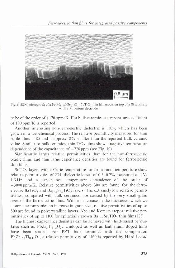
PLZT layers. The column width ofthe layers is larger than in the case ofthe PZTand PLZT layers and can thus be determined by SEM analysis. As shown inFig. 6, the column width for the relaxor thin films is of the order of 150-200 nm. We found that also here the column width remains for all layers con-stant and is always of the order of 150-200 nm. The column height increaseswith the film thickness (see Figs 7 and 8).
4. Electrical performance of oxidic thin films for integrated passive components
4.1. Capacitance as a function of material composition, doping, thickness andtemperature
Thin-film materials of various compositions have been studied with respectto their electrical performance. The non-ferroelectric Ta20s thin films show,similar to the bulk ceramics, a relative permittivity at room temperature of21.5. Relative permittivity and dielectric losses for these non-ferroelectriccapacitors are not dependent on the applied ac voltage as shown in Fig. 9.
The temperature dependence of these non-ferroelectric thin films has beenstudied in the temperature range of -55°C to 125 °C and is shown in Fig.10. The temperature dependence of these Ta20s films has been determined
374 Phillips .Ioumal of Research Vol. 51 No.3 1998
Phillips Journalof Research Vol. 51 NO.3 1998 375
Ferroelectric thin films for integrated passive components
Fig. 6. SEM micrograph of a Pb(Mg1/3 Nb2/3)OrPbTi03 thin film grown on top of a Si substratewith a Pt bottom electrode.
to be ofthe order of +170 ppm/K. For bulk ceramics, a temperature coefficientof lOOppm/K is reported.
Another interesting non-ferroelectric dielectric is Ti02' which has beengrown in a wet-chemical process. The relative permittivity measured for thinrutile films is 85 and is approx. 8% smaller than the reported bulk ceramicvalue. Similar to bulk ceramics, thin Ti02 films show a negative temperaturedependence of the capacitance of -720 ppm (see Fig. 10).
Significantly larger relative permittivities than for the non-ferroelectricoxidic films and thus large capcitance densities are found for ferroelectricthin films.
SrTiO} layers with a Curie temperature far from room temperature showrelative permittivities of 235, dielectric losses of 0.5-0.7% measured at 1V/I KHz and a capacitance temperature dependence of the order of-3000 ppm/K, Relative permittivities above 300 are found for the ferro-electric BaTiO} and Bal_xSrx TiO} layers. The extremely low relative permit-tivities, compared with bulk ceramics, are caused by the very small grainsizes of the ferroelectric films. With an increase in the thickness, which weassume accompanies an increase in grain size, relative permittivities of up to800 are found in polycrystalline layers. Abe and Komatsu report relative per-mittivities ofup to 1100 for epitaxially grown Bal_xSrrTiO} thin films [23].
The highest capacitance densities can be achieved with lead-based perovs-kites such as PbZrxTil_xO}. Undoped as well as lanthanum doped filmshave been studed. For PZT bulk ceramics with the compositionPbZrO.51TioA90}, a relative permittivity of 1160 is reported by Härdtl et al.

M. Klee et al.
(b)
Fig. 7. SEM micrograph of the surface (a) and the cross-section (b) of a 0.4 Jlm thickPbC(Mgl/3Nb2/3)03~PbTiOJ film grown on top of a platinised Si substrate.
376 Phillips Journalof Research Vol. 51 No.3 1998

Ferroelectric thin films for integrated passive components
(b)
Phillips Journalof Research Vol. SI No.3 1998 377
Fig. 8. SEM micrograph of the surface (a) and the cross-section (b) of a 0.8/1m thickPbCMgl/JNb2/J)OJ-PbTiOJ film grown on top of a platinised Si substrate.

M. Klee et al.
23~---------------------------------------- ~ 3
2,5
2
~- 1,5 ~III0....I
1
22,5
~~ 22
~8. 21,5 .J.e._....._--.---- ...~.,.,---...............- ......------- .......-I--~ I~
21&20,5 ~ _ - _ '" _ ...... __ .." ...... '" _ .......__ ...... _ _ 0,5
~ 00,12 0,22 0,32 0,42 0,52 0,62
acVoltageM
0,72 0,82 0,92
Fig. 9. Relative permittivity and dielectric losses as a function of the ac voltage for a thin Ta20Slayer grown on a Si substrate.
[17]. These data are found for poled bulk samples. With lanthanum doping ofPbZrO.51Tio.4903,the relative permittivity increases to 1570. For undoped bulkceramics, however, with the composition PbZro.53Tio.4703,Härdtl et al. [17]measured a permittivity of only 570. Lanthanum doping increases thepermittivity up to 2000. In the case of our undoped PbZro.53Tio.4703 films,grown in the modified sol-gel process, as well as for lanthanum doped filmswith 1-9% lanthanum doping, the relative permittivities are around
30 I Relativecapacitance ["k] I100 IC- C25)/C25
20Ti02 (-720 ppmlK)
10 Ta205 (170 ppmlK)
---1 0 -50 50 ,pft
2~-10IIN
ITemperature rCJI
-~-30
-40
Fig. 10. Relative capacitance as a function of temperature for a thin Ta20S layer and a thin Ti02layer grown on Si substrates.
378 PhilUpsJournalof Research Vol. SI No. 3 1998

Ferroelectric thin films for integrated passive components
1200 r------------------~ 3
ID> 400;;ca"äiD:: 200
01 3
.i!' 1000'>= 800~8.. 600
~--------------------- 2,5-------- .....__--.-j
2 '0'~1/1
1,5 :ll1/1
1 .3
0,5
05 7 9
Lanthanum content In PLZT films rio]
Fig. 11. Relative permittivity and dielectric losses as a function of lanthanum content forPbZrO.53Tio.4703films.
1100± 25 (see Fig. 11). The losses are of the order of 2.0-2.3%. These datahave been measured for unpoled thin-film samples. So we did not find a depen-dence of the relative permittivity from lanthanum doping as reported for bulkceramics with a similar composition.
Although the La doping does not affect the relative permittivity in thinPbZro.53Tio.4703 films, a thickness dependence of the relative permittivityhas been found. PbZro.53Tio.4703 films doped with a few percent lanthanumshow an increase ofthe relative permittivity from 950 for submicron thin filmsup to 1500 for films with a thickness of 6 J..Lm (see Fig. 12). The relative
1600r---------------------------------------------~1400
~ 1200·>Ë 1000E8. 800~:1:1 600<'Cl
~ 400
200
O+-----,_-----r----~----~------+_----~----~
-
r
o 1 2 3 4 5 6 7
Thickness of PLZT films [lJm]
Fig. 12. Relative permittivity of PbZrO.53Tio.4703 thin filmswith a few percent lanthanum dopingplotted as a function of film thickness.
Phillips Journal of Research Vol. SI No.3 1998 379
M. Klee et al.
-1 0
--11%La
---- 9%La
·······7%La
-.-.- 6%La
Relative capacitance [%]100 (C - C25)/C25
-50 100 150 2
ITemperature rC]1-20
-30
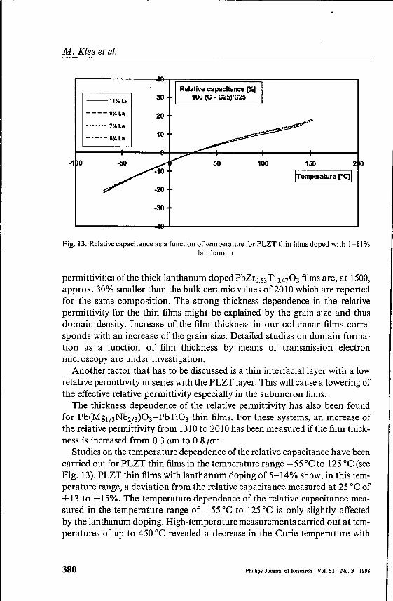
Fig. 13. Relative capacitance as a function oftemperature for PLZT thin fiims doped with 1-11%lanthanum.
permittivities ofthe thick lanthanum doped PbZro.53Tio.4703films are, at 1500,approx. 30% smaller than the bulk ceramic values of 2010 which are reportedfor the same composition. The strong thickness dependence in the relativepermittivity for the thin films might be explained by the grain size and thusdomain density. Increase of the film thickness in our columnar films corre-sponds with an increase of the grain size. Detailed studies on domain forma-tion as a function of film thickness by means of transmission electronmicroscopy are under investigation.
Another factor that has to be discussed is a thin interfaciallayer with a lowrelative permittivity in series with the PLZT layer. This will cause a lowering ofthe effective relative permittivity especially in the submicron films.
The thickness dependence of the relative permittivity has also been foundfor Pb(Mgl/3Nb2/3)OrPbTi03 thin films. For these systems, an increase ofthe relative permittivity from 1310to 2010 has been measured ifthe film thick-ness is increased from 0.3 pm to 0.8 uss».
Studies on the temperature dependence ofthe relative capacitance have beencarried out for PLZT thin films in the temperature range -55 oe to 125oe (seeFig. 13). PLZT thin films with lanthanum doping of 5-14% show, in this tem-perature range, a deviation from the relative capacitance measured at 25 oe of±13 to ±15%. The temperature dependence of the relative capacitance mea-sured in the temperature range of -55 oe to 125oe is only slightly affectedby the lanthanum doping. High-temperature measurements carried out at tem-peratures of up to 450°C revealed a decrease in the Curie temperature with
380 Phillips Journalof Research Vol. 51 No. 3 1998

Ferroelectric thin films Jar integrated passive components
6r-----------------------------------------~5
-PLZTfilm
.... 4 - - 8.TI03~:ll 3IIIIIIo..J 2
Fig. 14. Dielectric losses as a function of ac field strength for PLZT, BaTi03 and Ta20s thin films.
increasing lanthanum doping similar to bulk ceramics. In accordance withbulk ceramics, a broadening of the Curie temperature with increasing lantha-num has been found.
4.2. Dielectric losses as a Junction oJ ac voltage Jar ferroelectric thin films
In ceramic multilayer capacitors with dielectric thicknesses of 15JLm downto 5 JLm, the dielectric losses are typically specified to be below 3.5% at1Vrms/I KHz. For these very thick dielectric layers, these are small signalmeasurements; the applied field strength is of the order 0.6-2 kV/cm. In thethin-film application with submicron layers ofO.2-0.8 JLm, however, the speci-fication 1Vrms corresponds to large electrical fields of 12-50 kV/cm. The fieldstrength of 12-50 kV/cm applied on the ferroelectric thin film at 1V/I kHzexceeds the coercive fields strength of BaTi03 and PLZT. For that reason,larger dielectric losses are observed for thin-film ferroelectric capacitors com-pared with ceramic capacitors at the specification 1Vrms/I kHz. This is shownin Fig. 14.The dielectric losses ofPLZT thin films ofsubmicron thickness havebeen measured to be smaller than 2% at 1-2kV/cm/1 kHz and increase up to5.6% if an ac field of 15kV/cm is applied. For the BaTi03 thin films with slimhysteresis loops and thus lower dielectric losses compared with PZT and PLZTthin films, the dependence of the dielectric losses on the applied ac field is lesspronounced (see Fig. 14). For these films, the losses therefore increase from1.8% at 1-2kV/cm only up to 2.1% at20 kv/cm. No dependence ofthe dielec-tric losses on the applied field strength has been found for non-ferroelectric
- - • T0205
_---------- ------
...... _ - -- ..- ..... - -"".-_"_ - . ., ... ---o~--------~---------+----------~------~o 5 10
ac Field [kV/cm]
15 20
Philiips Journni of Research Vol. SI No.3 1998 381

M. Klee et al.
11501130
z:. 1110~ 1090ê 1070!. 1050~ 1030i11010" 990
970950
0
Slope = -2.12 % I decade
1 2 3' 4 5 6 7
log time [min]
Fig. 15. Permittivity plotted as a function of log time for PLZT thin films.
Ta20s thin films. The dielectric losses are of the order of 0.2-0.5% at an acfield strength of2-20kV/cm (see Fig. 14).
4.3. Ageing of ferroelectric thin films of various compositions
As discussed in Sec. 2.2, ageing (drop of the relative permittivity with time)is well known in conventional CMCs and is dependent on the dielectricmaterial system; ageing rates of 1-8% are observed. For certain applica-tions, a minimum ageing rate is required that must not to exceed 3%. Ageingrates of thin films have not been reported until now. We studied the ageingproperties of ferroelectric thin films of various compositions. The results aregiven in Fig. 15 (plot of permittivity versus log time). For PLZT samplesde-aged at 350°C, an ageing rate of -2.1 % to -2.4% has been measured.The ageing rate agrees with the data reported for bulk ceramics by Furukawaet al. [24].
382 Phillips Journni of Research Vol. 51 No. 3 1998
4.4. Insulation resistance, breakdown voltage and lifetime of ferroelectric thin-film capacitors
Ferroelectric multilayer capacitors are usually specified with an insulationresistance above 100 gigaohm (measured at room temperature) if ratedvoltage is applied for 60 s. For capacitors with dielectric thicknesses of 5-15J.1,ffiand rated voltages of 16-50V, a field strength of 30kV/cm is usuallyapplied. Thin film ferroelectric capacitors with submicron thicknesses whichshould be specified for maximum 16V have therefore to withstand an

Phillips Journalof Research Vol. SI No.3 1998 383
Ferroelectric thin films for integrated passive components
electrical field strength of approx. 100-400 kV/cm. In Fig. 16 the current den-sity is given as a function of field strength for lanthanum doped PLZT films.The PLZT films show low current densities of 10-8 A/cm2 for both polaritiesand are therefore high ohmic (>100 gigaohm). The breakdown field strengthhas been determined to be of the order of 1.2-1.6 MV[cu».
Another important material specification for ceramic capacitors is their life-time. Ceramic capacitor data books specify that the capacitor has to withstandrated voltages at upper category temperatures for more than 1000hours with-out deterioration of capacitor performance (capacitance, tanD). Endurancetests are therefore standard for ceramic capacitor products. To check thematerial performance and device performance in a limited time schedule,accelerated lifetime tests accompany endurance tests. Voltage and tempera-ture stress exceed the specified values.
Ferroelectric thin films have to fulfil the endurance performance in order tobe suited to capacitor applications. We studied in more detail, for undopedand lanthanum doped PZT capacitors and integrated passive componentmodules, the endurance as well as the lifetime under accelerated conditions.Measurements have been carried out at de fields of lOV/p,m, 20V/p,m and30Vpsi: in the temperature range of 310°C down to 85°C. The resistance
Current density[A/cm2]10-1~------------------ ~
v : on bottom
10-2
10-3
10-7
10-8
V- on top10-5
10-6
10-9~ ~~._ ~~~ ~ __~
10 100 1000 10000
Field strength [kV/cm]Fig. 16. Current density as a function of the field strength for lanthanum doped PZT thin-film
capacitors (measured at room temperature).

M. Klee et al.
10000000
1000000
100000
10000;Sal 1000E
~ 100..J
10
0,1
3151·c ! 20~'C i 121,·C ! ·c
~:=~J=EE~=~:=tj!:::=..-......--..--.-I...- ..-.--.JI ..---.-..-..--..~·~·~:!!-~~~_L.3~v/jlm·-·-· ..l·..·..··-··..·..·······
. I...·......···········_....-j··..······ ·_..·..l....·····..·-·;.;;-~-i···..··_··---..·l·_..·_·..·_..·····j-···..··..····_·..·..·.......................... .1. _ ,...... _ ·../'r···· ·..·..·..· _·~··-···..· ··..·······,·.._ · , .
I I" I i i iI " . I I·_·_·_·_······..·_·_·_·1· ········..· ·_···*··_·_·_·_·······,····_·..f··_·,········..·_-_·_·_·--i·.,··--·_·_·_·_·_······_-i·_·_·_··_···__····_·_·_'i· -_._._._._ ..I ./! ! ! I !
_ ···_ j;7··.._ _.._·f ·+ · _·_..t..· _····-·-1 ··_ ·_..·+·· ····..__·..·_··. I i 1 i !
0,01 -l----+----4----+---4----+---!---~1,5 1,7 1,9 2,1 2,3 2,5 2,7 2,9
10001T [11K]
Fig. 17. Lifetime plotted as a function of IOOO/T on a log/log scale. Measurements were carried outfor PLZT thin films.
was continuously monitored during measurement. The lifetime was defined asthe time when the resistance has dropped by one decade. In Fig. 17, the lifetimehas been plotted as a function of 10001T. In the log/log plot shown in Fig. 17,the lifetime is similar to bulk ceramics linearly dependent on liT. This holdsfor field strengths of 10V/pm, 20V//-Lm and 30V//-Lm. For temperatures of270-190 oe, lifetimes of 1 hour up to several hundred hours are found at afield strength of 20 VI /-Lm (see Fig. 17). Extrapolation of these data revealed,for temperatures of 125oe, lifetimes of more than 10000 hours. For fieldstrengths of 30V//-Lm, the lifetime is decreased to 0.2-40 hours in the tempera-ture range of 270-190 oe. Also for this high field strength of 30VI /-Lm, extra-polation ofthe data down to 125oe revealed lifetimes above 1000hours. Thesedata demonstrate that ferroelectric capacitors show, at 125-85 oe, an endur-ance of more than 1000 hours if high electrical field strengths of 10-30 VIusx: are applied.
384 Phillips Journalor Research Vol. SI No.3 1998
5. Conclusions
Integration of passive components can be achived by making use of thin-film processes for capacitors, resistors and inductors. Si is an attractive sub-strate material due to its high surface quality, high temperature stability andthermal expansion. Passive-only networks with component densities of 100-150 components/cm/ and high precision can be realised based on thin-filmtechniques. Resistors are based on conventional thin-film materials such as

Phillips Journal of Research Vol. SI No.3 1998 385
Ferroelectric thin films for integrated passive components
TiW(N). Thin-film capacitors can be realised with numerous thin-film dielec-trics. Dependent on the application range, dielectric layers with a low relativepermittivity such as Si3N4. Ta20S and Ti02 can be applied to thin-filmcapacitors. An extension of the application range can be achieved with ferro-electric materials based on earth alkaline titanate as well as lead based perov-skite layers such as PZT, PLZT or PMN. Relative permittivities of 200 up to2000 and capacitance densities of some tenths of a nF per mrrr' are typical sothat the capacitance range can be extended to several tenths of a nf', Amodified sol-gel process has been applied to the complex oxidic layers. Thecapacitor performance studied for films on Si substrates with nobel metal elec-trodes revealed typical capacitor specifications. Dependent on material com-position, relative permittivities of 25 up to 2000 have been found. Insulationresistances measured at room temperature are of the order of 1-3 x 10¹²ohm and breakdown fields of 1.2-1.6 MVlcm have been determined.Endurance and accelerated lifetime measurements revealed for ferroelectricthin films lifetimes of more than 1000 hours if high electrical fields of 10-30 VIf.Lm are applied.
Acknowledgements
We gratefully acknowledge the technical assistance by W. Brand andH. Hünten as well as the analytical characterizations carried out by D. Bausenand B. Krafczyk.
REFERENCES[I] P.H.M. Keizer and W. de Wild, Electroceramics IV, 1045, 1995.[2] In Proceedings of the BPA Worldwide Conference on Major Implications for Interconnee-
tion and Packaging, October 1996, Paris, France.[3] B. Milson et al., Philips J. Res., this issue.[4] M. de Samber et al., Philips J. Res., this issue.[5] A. Noma, JEE, 101-104, 1993.[6] J.V. Brook et al., Philips J. Res., this issue.[7] P.K. Larsen, R. Cuppens, G.C.A.M. Spierings, Ferroelectrics, 128,265, 1992.[8] R. Waser, M. Klee, Integrated Ferroelectrics, 2, 23, 1992.[9] U. Robeis, Alterungserscheinungen in ferroelektrischer Keramik, Verlag Mainz, 1993.[10] T. Schrout, Ferroelectrics, 9(3),361, 1989.[11] U. Harada, J. Kanai, Y. Yamashita, J. Am. Ceram. Soc, 79(8), 2109-12, 1996.[12] M. Klee, R. Eusemann, R. Waser, W. Brand, H. van Hal, J. Appl. Physics, 72, 1566, 1992.[I3] M. Klee, U. Mackens, J. Pankert, W. Klee, in Science of Technology of Electroceramic Thin
Films, 99-115, 1995.[14] M. Huffmann, Integrated Ferroelectrics, 10(1-4), 39, 1995.[15] G.J. Dormans, M. De Keiser, P.J.V. Veldhovem, D.M. Frigo, J.E. Holewign, G.P.M. Nie,
C.J. Smit, Chem. Mat., 5, 448,1993.[16] G. Haertling, J. Am Ceram. Soc., 54, 1-11, 1971.[17] K.C. Carl, K.H. Härdtl, Ber. Dr. Keram. Ges., 47,687,1970.

M. Klee et al.
[18] R.W. Schwartz, J.A. Voigt, B.A. TuttIe, R.S. DaSalla, submitted to J. Mat. Res.[19] M. Klee, A. De Veirman, U. Mackens, Philips J. Res. 47, 263, 1993.[20] L.F. Francis, D.A. Payne, J. Am Ceram. Soc., 74(12), 3000, 1991.[21] K. Okuwada, S. Nakamura, M. Imai, K. Kakumo, Mal. Res. Soc. Symp. Proc., 204, 557~
562, 1991.[22] K. Okuwada, M. Imai, K. Kakumo, Ceram. Trans., 23, 713~718, 1991.[23] K. Abe, S Komatsu, J. Appl. Phys., 77(12) 6461~6465, 1995.[24] O. Furukawa, H. Kanai, Y. Yamashita, Jpn. J. Appl. Phys., 32, 1708~1711, 1993.
Authors' Biographies
386
Mareike Klee studied chemistry at the TH Darmstadt (l976~1984) andreceived here Ph.D. in inorganic structure and solid-state chemistry. In1984 she joined the Electronic Ceramics Group of the Philips ResearchLaboratories, Aachen. She started with investigations on wet-chemicalpower-preparation techniques and made use of this experience to build-up the electroceramic thin-film processing capability at Philips ResearchLaboratories, Aachen. Her activities include the development and char-acterisation of ferroelectric, pyroelectric and piezoelectric thin films forintegrated passive components, non-volatile memories, pyroelectric sen-sors and piezoelectric actuators.
Uwe Mockens received his Ph.D. degree in physics from the University ofHamburg in 1986, where he studied electronic excitation in microstruc-tured two-dimensional silicon MOS systems. In 1985 he joined the Ph i-lips Research Laboratory Hamburg to work on X-ray lithography. Hewas mainly involved in the fabrication of sub-half-micron devices andrelated topics. In 1991 he joined the Electronic Ceramics Group of thePhilips Research Laboratory, Aachen. He evaluated ferroelectric thinfilms for non-volatile memories and integrated passive components.At present he is responsible for the quality and reliability of the filmcomponents.
Rainer Kie wit I studied electrical engineering at the FH Aachen (1990~1994). He finished his study with a diploma thesis at the Dublin InstituteofTechnology on tuning of Fuzzy Control Systems. In 1995 hejoined theElectronic Ceramics Group of the Philips Research Laboratories,Aachen. He is involved in the development, electrical characterisationand simulation of thin-film components.
Phillips Journalof Research Vol. 51 No. 3 1998

Ferroelectric thin .films for integrated passive components
Georg Greuel studied electronics at the RWTH Aachen (1981-1987). Hefinished his study with a diploma thesis on contour/texture picture codingalgorithms. In 1987 he joined the Electronic Ceramics Group of the Phi-lips Research Laboratories, Aachen. He investigated reliability predic-tion methods for wet electrolytic aluminium oxide layers and finishedthese studies with his thesis on the dielectric breakdown of aluminiumoxide layers. Since 1993, G. Greuel has been project leader of the reliabil-ity cluster, working on yield improvement, new test methods and descrip-tion of failure modes in passive ceramic components.
Christof Metzmacher studied mineralogy with an emphasis on crystallo-graphy at the RWTH Aachen (1989-1995). In 1995 he performed at theInstitute of Solid State Research, Research Centre Juelich (Germany),transmission electron microscopy investigations on plastically deformedsingle quasicrystals. In 1996 he joined the Electronic Ceramics Groupofthe Philips Research Laboratories, Aachen. He is involved in the devel-opment and characterisation of electronic ceramics such as PTCs, ferritesand ceramic thin films by means of TEM studies.
Phillips Journalof Research Vol. 51 No.3 1998 387