features description Î block diagram
TRANSCRIPT

1www.diodes.com October 2020
Diodes IncorporatedPI6CB332001 Document Number DS42049 Rev 5-2
FeaturesÎÎ Supports Intel's DB2000QL specÎÎ 3.3V supply voltageÎÎ HCSL input: 100MHz (typ), up to 400MHzÎÎ 20 differential low power HCSL outputs with on-chip
terminationÎÎ Two output enable control modesÎy Traditional 8 OE# pins and 20 SMBus bitsÎy Simple 3-wire Side-Band interface real-time controlÎÎ SMBus interface supportÎÎ Spread spectrum tolerantÎÎ Very low jitter outputsÎy Differential additive phase jitter: DB2000Q <30fs RMSÎy Differential additive phase jitter: PCIe Gen4 <30fs RMSÎy Differential additive phase jitter: PCIe Gen5 <20fs RMSÎy PCIe Gen1/Gen2/Gen3/Gen4/Gen5 compliantÎÎ Differential output-to-output skew <50psÎÎ Low propagation delay: <3nsÎÎ Industrial temperature support: -40°C to 85°CÎÎ Totally Lead-Free & Fully RoHS Compliant (Notes 1 & 2)ÎÎ Halogen and Antimony Free. “Green” Device (Note 3)ÎÎ For automotive applications requiring specific change control
(i.e. parts qualified to AEC-Q100/101/200, PPAP capable, and manufactured in IATF 16949 certified facilities), please contact us or your local Diodes representative.
https://www.diodes.com/quality/product-definitions/ÎÎ Packaging (Pb-free & Green): Îy 80-lead 6x6mm dual-row aQFN
Description The PI6CB332001 is a 20-output very low power PCIe Gen1/ Gen2/Gen3/Gen4/Gen5 clock buffer. It is capable of distributing the reference clocks for UPI, SAS, SATA, and other applications as well. It takes an reference input to fanout twenty 100MHz low power differential HCSL outputs with on-chip terminations. The on-chip termination can save 80 external resistors and make lay-out easier. OE pins combined with SMBus bits as well as 3-wire side band interface provide easier power management for each output. It uses Diodes' proprietary design to achieve very low jitter that meets PCIe Gen1/Gen2/Gen3/Gen4/Gen5 requirement.
A Product Line ofDiodes Incorporated
PI6CB332001
20-Output PCIe Gen4/Gen5 Clock Buffer With On-chip Termination
Block Diagram
IN+IN-
SA_0SA_1SCLK
SDATA
PWRGD/PWRDN#OE#[7:9, 11, 12]
OE5#/DATAOE6#/CLK
OE10#/SHFT_LD#
SBEN
Q19+
Q19-
Q0+
Q0-
VDDA VDDO
Control Logic
SMBusEngine
Notes: 1. No purposely added lead. Fully EU Directive 2002/95/EC (RoHS), 2011/65/EU (RoHS 2) & 2015/863/EU (RoHS 3) compliant. 2. See https://www.diodes.com/quality/lead-free/ for more information about Diodes Incorporated’s definitions of Halogen- and Antimony-free, "Green" and Lead-free. 3. Halogen- and Antimony-free "Green” products are defined as those which contain <900ppm bromine, <900ppm chlorine (<1500ppm total Br + Cl) and <1000ppm
antimony compounds.
bPLead-free Green

22
A Product Line ofDiodes Incorporated
PI6CB332001
www.diodes.com October 2020 Diodes Incorporated
PI6CB332001 Document Number DS42049 Rev 5-2
Pin DescriptionPin Number Pin Name Type Description
A1 Q17+ Output HCSL Differential true clock output
A2 Q16- Output HCSL Differential complementary clock output
A3 Q16+ Output HCSL Differential true clock output
A4 Q15- Output HCSL Differential complementary clock output
A5 Q15+ Output HCSL Differential true clock output
A6 Q14- Output HCSL Differential complementary clock output
A7 Q14+ Output HCSL Differential true clock output
A8 Q13- Output HCSL Differential complementary clock output
A9 Q13+ Output HCSL Differential true clock output
A10 Q12- Output HCSL Differential complementary clock output
Pin Configuration
Q17+
Q17-
Q18+
Q18-
Q19+
Q19-
IN+
IN-
Q0+
Q0-
Q1+
Q1-
Q16-
VDDO
NC
NC
SBEN
NC
NC
VDDA
NC
NC
VDDO
Q2+
Q16+
NC
Q15-
SA_0
Q15+
NC
Q14-
VDDO
Q14+
NC
Q13-
SA_1
Q13+
NC
Q12-
OE12#
Q12+
VDDO
Q11-
Q11+
OE11#
NC
OE10#/SH-FT_LD#
NC
NC
OE8#
NC
OE7#
VDDO
Q6+
Q10-
Q10+
OE9#
Q9-
Q9+
Q8-
Q8+
Q7-
Q7+
Q6-
NC
Q2-
SDATA
Q3+
SCLK
Q3-
NC
PWRGD/PWRDN#
NC
Q4+
OE5#/DATA
Q4-
NC
Q5+
OE6#/CLK
Q5-
EPAD is GND
1 2 3 4 5 6 7 8 9 10 11 12
A
B
C
D
E
F
G
H
J
K
L
M
33
A Product Line ofDiodes Incorporated
PI6CB332001
www.diodes.com October 2020 Diodes Incorporated
PI6CB332001 Document Number DS42049 Rev 5-2
Pin Description Cont.Pin Number Pin Name Type Description
A11 Q12+ Output HCSL Differential true clock output
A12 Q11- Output HCSL Differential complementary clock output
B1 Q17- Output HCSL Differential complementary clock output
B2 VDDO Power Power supply for outputs, nominal 3.3V
B3 NC No connect
B4 SA_0 Input CMOS
SMBus address bit. This is a tri-level input that works in conjunction with SA_1 pin, if present, to decode SMBus addresses. It has internal pull-up/down resistors to bias to VDD/2. See the SMBus Address Selec-tion table.
B5 NC No connectB6 VDDO Power Power supply for outputs, nominal 3.3VB7 NC No connect
B8 SA_1 Input CMOS
SMBus address bit. This is a tri-level input that works in conjunction with SA_0 pin, if present, to decode SMBus addresses. It has internal pull-up/down resistors to bias to VDD/2. See the SMBus Address Selec-tion table.
B9 NC No connect
B10 OE12# Input CMOS Active low input for enabling Q12 pair. 1 =disable outputs, 0 = enable outputs. The pin has internal pull down
B11 VDDO Power Power supply for outputs, nominal 3.3V
B12 Q11+ Output HCSL Differential true clock output
C1 Q18+ Output HCSL Differential true clock output
C2 NC No connect
C11 OE11# Input CMOS Active low input for enabling Q11 pair. 1 =disable outputs, 0 = enable outputs. The pin has internal pull down
C12 Q10- Output HCSL Differential complementary clock output
D1 Q18- Output HCSL Differential complementary clock output
D2 NC No connectD11 NC No connectD12 Q10+ Output HCSL Differential true clock output
E1 Q19+ Output HCSL Differential true clock output
E2 SBEN Input CMOS
Input that enables the Side-Band Interface for controlling output enables. This pin disables the output enable pins when asserted. It has an internal pull-down resistor.0 = OE pins and SMBus enable bits control outputs, Side-band interface disabled.1 = Side-Band Interface controls output enables, OE pins and SMBus en-able bits are disabled
44
A Product Line ofDiodes Incorporated
PI6CB332001
www.diodes.com October 2020 Diodes Incorporated
PI6CB332001 Document Number DS42049 Rev 5-2
Pin Description Cont.Pin Number Pin Name Type Description
E11 OE10#/SHFT_LD# Input CMOS
Active low input for enabling output 10 or SHFT_LD- pin for the Side-Band Interface. Refer to the Side-Band Interface section for details. This pin has an internal pull-down.OE mode: 1 = disable output, 0 = enable output.Side-Band Mode: 1 = enable Side-Band Interface shift register, 0 = disableSide-Band Interface shift register. A falling edge transfers Side-Band shift register contents to output register
E12 OE9# Input CMOS Active low input for enabling Q9 pair. 1 =disable outputs, 0 = enable outputs. The pin has internal pull down
F1 Q19- Output HCSL Differential complementary clock output
F2 NC No connectF11 NC No connect
F12 Q9- Output HCSL Differential complementary clock output
G1 IN+ Input HCSL Differential true clock input
G2 NC No connectG11 NC No connect
G12 Q9+ Output HCSL Differential true clock output
H1 IN- Input HCSL Differential complementary clock input
H2 VDDA Power Power supply for inputs and analog circuits, nominal 3.3V
H11 OE8# Input CMOS Active low input for enabling Q8 pair. 1 =disable outputs, 0 = enable outputs. The pin has internal pull down
H12 Q8- Output HCSL Differential complementary clock output
J1 Q0+ Output HCSL Differential true clock output
J2 NC No connectJ11 NC No connectJ12 Q8+ Output HCSL Differential true clock outputK1 Q0- Output HCSL Differential complementary clock outputK2 NC No connect
K11 OE7# Input CMOS Active low input for enabling Q7 pair. 1 =disable outputs, 0 = enable outputs. The pin has internal pull down
K12 Q7- Output HCSL Differential complementary clock outputL1 Q1+ Output HCSL Differential true clock outputL2 VDDO Power Power supply for outputs, nominal 3.3VL3 NC No connectL4 SDATA I/O CMOS SMBus data pinL5 SCLK Input CMOS SMBus clock pinL6 NC No connectL7 NC No connect

55
A Product Line ofDiodes Incorporated
PI6CB332001
www.diodes.com October 2020 Diodes Incorporated
PI6CB332001 Document Number DS42049 Rev 5-2
Pin Description Cont.Pin Number Pin Name Type Description
L8 OE5#/DATA Input CMOS
Active low input for enabling output 5 or the data pin for the Side-Band Interface. Refer to the Side-Band Interface section for details. This pin has an internal pull-down.OE mode: 1 = disable output, 0 = enable output.Side-Band mode: Data pin
L9 NC No connect
L10 OE6#/CLK Input CMOS
Active low input for enabling output 6 or the clock pin for the Side-Band Interface shift register. Refer to the Side-Band Interface section for de-tails. This pin has an internal pull-down.OE mode: 1 = disable output, 0 = enable output.Side Band mode: Clocks data into the Side-Band Interface shift register on the rising edge
L11 VDDO Power Power supply for outputs, nominal 3.3V
L12 Q7+ Output HCSL Differential true clock output
M1 Q1- Output HCSL Differential complementary clock output
M2 Q2+ Output HCSL Differential true clock output
M3 Q2- Output HCSL Differential complementary clock output
M4 Q3+ Output HCSL Differential true clock output
M5 Q3- Output HCSL Differential complementary clock output
M6 PWRGD/PWRDN# Input CMOS
Input notifies device to sample latched inputs and start up on first high assertion. Low enters Power Down mode, subsequent high assertions exit Power Down mode. This pin has internal pull-down resistor
M7 Q4+ Output HCSL Differential true clock output
M8 Q4- Output HCSL Differential complementary clock output
M9 Q5+ Output HCSL Differential true clock output
M10 Q5- Output HCSL Differential complementary clock output
M11 Q6+ Output HCSL Differential true clock output
M12 Q6- Output HCSL Differential complementary clock output
EPAD Power Connect to Ground
66
A Product Line ofDiodes Incorporated
PI6CB332001
www.diodes.com October 2020 Diodes Incorporated
PI6CB332001 Document Number DS42049 Rev 5-2
SMBus Address Selection Table
SA_1 SA_0 Address
L L D8
L M DA
L H DE
M L C2
M M C4
M H C6
H L CA
H M CC
H H CE
Output Control - SBEN=0 Inputs OE# Pins and Register Bits Side Band Interface
PWRGD/PWRDN# IN+/IN- SMBUS Enable Bit OE# Pin
MASKx Byte[10:8] Dx Q+/Q- [19:0]
0 X X X X X Low/Low
1 Running
0 X X X Low/Low
1 0 X X Running
1 1 X X Low/Low
1 Stopped1 0 X X Stopped
1 1 X X Low/Low
Output Control - SBEN=1 Inputs OE# Pins and Register Bits Side Band Interface
PWRGD/PWRDN# IN+/IN- SMBUS Enable Bit OE# Pin
MASKx Byte[10:8] Dx Q+/Q- [19:0]
0 X X X X X Low/Low
1 Running
X X 0 0 Low/Low
X X 0 1 Running
X X 1 X Running
1 Stopped
X X 0 0 Low/Low
X X 0 1 Stopped
X X 1 X Stopped
77
A Product Line ofDiodes Incorporated
PI6CB332001
www.diodes.com October 2020 Diodes Incorporated
PI6CB332001 Document Number DS42049 Rev 5-2
Output Enable Control on PI6CB332001The 20-output PI6CB332001 has two methods for enabling and disabling outputs. The first is the traditional method of OE# pins and SMBus output enable bits. The second method is a simple 3-wire serial interface referred to as the Side-Band Interface (SBI). Both interfaces are not active at the same time, and the SBEN pin selects which interface is active. Tying the SBEN high enables the SBI. Tying the SBEN pin low enables the traditional OE# pin/SMBus output enable interface. Both the SBI and the traditional interface feed common output enable/disable synchronization logic ensuring glitch free enable and disable of outputs, regardless of the method used.
Traditional MethodOutputs 5 through 12 have dedicated output enable pins and each of the 20 outputs has dedicated SMBus output enable bits in Byte0, Byte1, and Byte2 of the SMBus register set.
Side-Band InterfaceThis interface consists of DATA, CLK and SHFT_LD# pins. When the SHFT_LD# pin is high, the rising edge of CLK can shift DATA into the shift register. After shifting data, the falling edge of SHFT_LD# clocks the shift register contents to the Output register. When the SBI is enabled, OE[7:9, 11, 12]# are disabled and DATA, CLK, and SHFT_LD# are enabled on OE5#, OE6# and OE10# respectively. Additionally, SMBus registers for masking off the disable function of the shift register (0 value of a bit) become active. When set to a one, the mask register forces its respective output to 'enabled.' This prevents accidentally disabling critical outputs when using the SBI.An SMBus read back bit in Byte 4 indicates which output enable control interface is enabled.When the SBI is enabled, and power has been applied, the SBI is active, even if the PWRGD/PWRDN# pin indicates the part is in power down. This allows loading the shift register and transferring the contents to the output register before the assertion of PWRGD. Note that the mask registers are part of the normal SMBus interface and cannot be accessed when the PWRGD/PWRDN# is low. Figure 1 provides a functional description of the SBI.The SBI and the traditional SMBus output enable registers both default to the 'output enabled' state at power-up. The mask registers default to zero at power-up, allowing the shift bits to disable their respective output. See Figure 1.
Mask 0
Mask 1
Mask 19
Byte 8 Byte 9 Byte 10
SMBus Mask Registers(Default is ‘0’)
To Output Logic
OE0 OE19OIO
DOE1
OIO
D
OIO
D
OIOD
OIOD
OIOD
D0 D1 D19
to D2from D18
DATA
CLKSHFT_LD#
OutputRegister
(Default is 1)
ShiftRegister
Side-Band Interface
Figure 1. Side Band Interface Control Logic Description
88
A Product Line ofDiodes Incorporated
PI6CB332001
www.diodes.com October 2020 Diodes Incorporated
PI6CB332001 Document Number DS42049 Rev 5-2
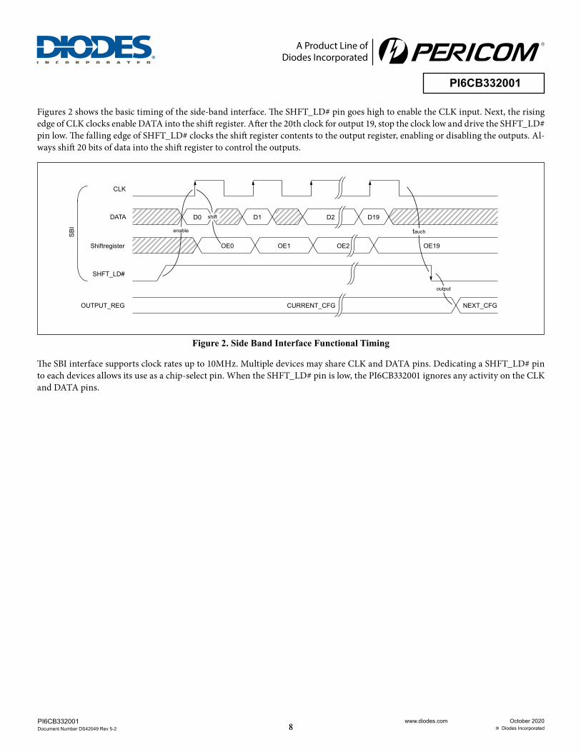
Figures 2 shows the basic timing of the side-band interface. The SHFT_LD# pin goes high to enable the CLK input. Next, the rising edge of CLK clocks enable DATA into the shift register. After the 20th clock for output 19, stop the clock low and drive the SHFT_LD# pin low. The falling edge of SHFT_LD# clocks the shift register contents to the output register, enabling or disabling the outputs. Al-ways shift 20 bits of data into the shift register to control the outputs.
The SBI interface supports clock rates up to 10MHz. Multiple devices may share CLK and DATA pins. Dedicating a SHFT_LD# pin to each devices allows its use as a chip-select pin. When the SHFT_LD# pin is low, the PI6CB332001 ignores any activity on the CLK and DATA pins.
enable
output
tauch
CLK
DATA
Shiftregister
SHFT_LD#
OUTPUT_REG
SB
I
D0 D1 D2 D19
OE0 OE1 OE2 OE19
CURRENT_CFG NEXT_CFG
shift
Figure 2. Side Band Interface Functional Timing
99
A Product Line ofDiodes Incorporated
PI6CB332001
www.diodes.com October 2020 Diodes Incorporated
PI6CB332001 Document Number DS42049 Rev 5-2
PWRDN# Assertion
PWRGD Assertion
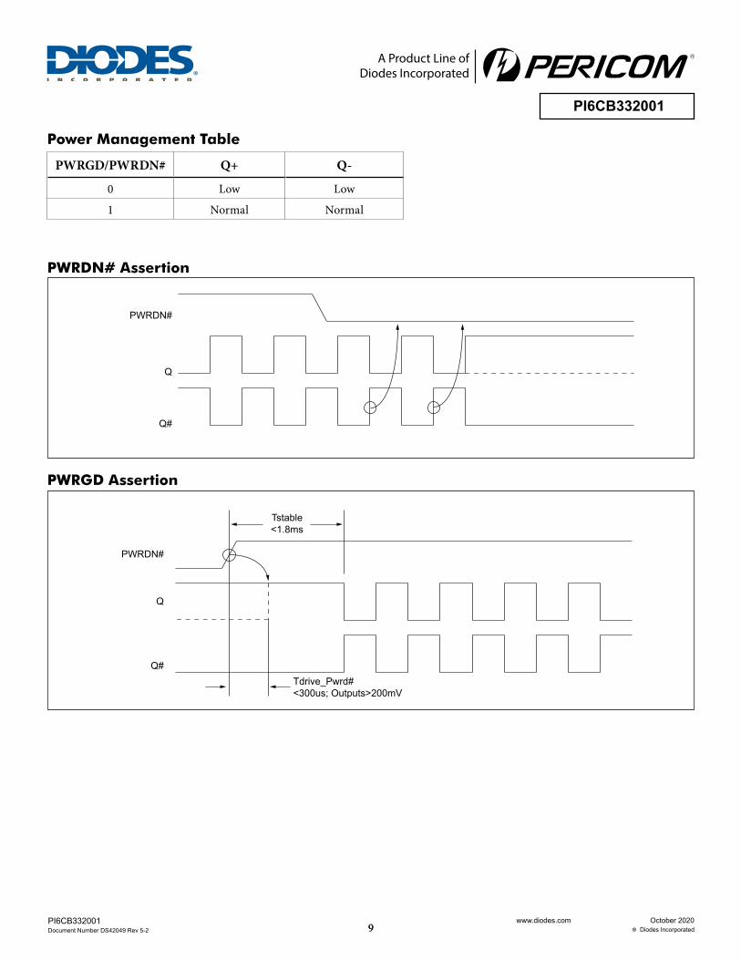
Power Management Table
PWRGD/PWRDN# Q+ Q-
0 Low Low
1 Normal Normal
PWRDN#
Q
Q#
PWRDN#
Q
Q#
Tstable<1.8ms
Tdrive_Pwrd#<300us; Outputs>200mV
1010
A Product Line ofDiodes Incorporated
PI6CB332001
www.diodes.com October 2020 Diodes Incorporated
PI6CB332001 Document Number DS42049 Rev 5-2
Storage Temperature .......................................................... –65°C to +150°CSupply Voltage to Ground Potential, VDDxx ..................–0.5V to +4.0VInput Control Pins Voltage ........................................ –0.5V to VDD+0.5V CLK+/- pins ................................................................................-0.5V to 2.5VSMBus, Input High Voltage .................................................................... 3.6VESD Protection (HBM) ...................................................................... 2000V Junction Temperature ..................................................................125 °C max
Note:
Stresses greater than those listed under MAXIMUM RATINGS may cause permanent damage to the device. This is a stress rating only and functional operation of the device at these or any other conditions above those indicated in the operational sections of this specification is not implied. Exposure to ab-solute maximum rating conditions for extended periods may affect reliability.
Maximum Ratings(Above which useful life may be impaired. For user guidelines, not tested.)
Operating ConditionsTemperature = TA; Supply voltages per normal operation conditions; See test circuits for the load conditions
Symbol Parameters Conditions Min. Typ. Max. Units
VDD, VDD_A Power Supply Voltage 3.135 3.3 3.465 V
IDD Power Supply Current VDD + VDDA, All outputs active @100MHz 160 200 mA
IDD_PDPower Supply Power Down(1) Cur-rent
VDD + VDDA, All outputs LOW/LOW 3 5 mA
TA Ambient Temperature Industrial grade –40 85 °C
Note:1. Input clock is not running.
Input Electrical Characteristics Symbol Parameters Conditions Min. Typ. Max. Units
Rpu Internal pull up resistance 120 KW
Rdn Internal pull down resistance 120 KW
LPIN Pin inductance 7 nH
1111
A Product Line ofDiodes Incorporated
PI6CB332001
www.diodes.com October 2020 Diodes Incorporated
PI6CB332001 Document Number DS42049 Rev 5-2
SMBus Electrical Characteristics Temperature = TA; Supply voltages per normal operation conditions; See test circuits for the load conditions
Symbol Parameters Conditions Min. Typ. Max. Units
VDDSMB Nominal bus voltage 2.7 3.6 V
VIHSMB SMBus Input High VoltageSMBus, VDDSMB = 3.3V 2.1 3.6
VSMBus, VDDSMB < 3.3V 0.65
VDDSMB
VILSMB SMBus Input Low VoltageSMBus, VDDSMB = 3.3V 0.6
VSMBus, VDDSMB < 3.3V 0.6
ISMBSINK SMBus sink current SMBus, at VOLSMB 4 mA
VOLSMB SMBus Output Low Voltage SMBus, at ISMBSINK 0.4 V
fMAXSMB SMBus operating frequency Maximum frequency 400 kHz
tRMSB SMBus rise time (Max VIL - 0.15) to (Min VIH + 0.15) 1000 ns
tFMSB SMBus fall time (Min VIH + 0.15) to (Max VIL - 0.15) 300 ns
LVCMOS DC Electrical Characteristics Temperature = TA; Supply voltages per normal operation conditions; See test circuits for the load conditions
Symbol Parameters Conditions Min. Typ. Max. Units
VIH Input High Voltage Single-ended inputs, except tri-level pins 2VDD +0.3
V
VIL Input Low Voltage Single-ended inputs, except tri-level pins -0.3 0.8 V
VIH Input High Voltage Single-ended tri-level inputs 2.4VDD +0.3
V
VIM Input Mid Voltage Single-ended tri-level inputs 1.3 0.5VDD 1.8 V
VIL Input Low Voltage Single-ended tri-level inputs -0.3 0.9 V
IIH Input High Current Single-ended inputs, VIN = VDD 5 mA
IIL Input Low Current Single-ended inputs, VIN = 0V -5 mA
IIH Input High Current Single-ended inputs with pull up resistor,VIN = VDD
50 mA
IIL Input Low Current Single-ended inputs with pull up resistor,VIN = 0V -50 mA
CIN Input Capacitance 1.5 5 pF
tRF Rise/ Fall time of Input 5 ns
1212
A Product Line ofDiodes Incorporated
PI6CB332001
www.diodes.com October 2020 Diodes Incorporated
PI6CB332001 Document Number DS42049 Rev 5-2
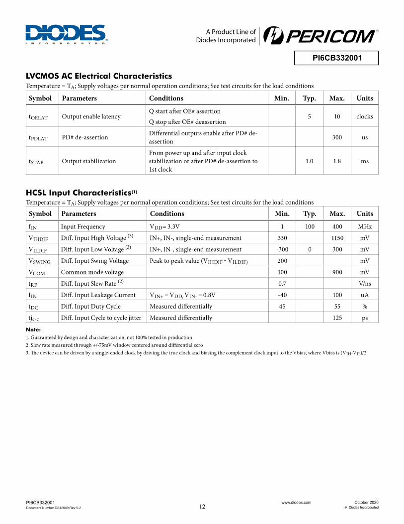
HCSL Input Characteristics(1) Temperature = TA; Supply voltages per normal operation conditions; See test circuits for the load conditions
Symbol Parameters Conditions Min. Typ. Max. Units
fIN Input Frequency VDD= 3.3V 1 100 400 MHz
VIHDIF Diff. Input High Voltage (3) IN+, IN-, single-end measurement 330 1150 mV
VILDIF Diff. Input Low Voltage (3) IN+, IN-, single-end measurement -300 0 300 mV
VSWING Diff. Input Swing Voltage Peak to peak value (VIHDIF - VILDIF) 200 mV
VCOM Common mode voltage 100 900 mV
tRF Diff. Input Slew Rate (2) 0.7 V/ns
IIN Diff. Input Leakage Current VIN+ = VDD, VIN- = 0.8V -40 100 uA
tDC Diff. Input Duty Cycle Measured differentially 45 55 %
tjc-c Diff. Input Cycle to cycle jitter Measured differentially 125 ps
Note:1. Guaranteed by design and characterization, not 100% tested in production2. Slew rate measured through +/-75mV window centered around differential zero3. The device can be driven by a single-ended clock by driving the true clock and biasing the complement clock input to the Vbias, where Vbias is (VIH-VIL)/2
LVCMOS AC Electrical Characteristics Temperature = TA; Supply voltages per normal operation conditions; See test circuits for the load conditions
Symbol Parameters Conditions Min. Typ. Max. Units
tOELAT Output enable latencyQ start after OE# assertionQ stop after OE# deassertion
5 10 clocks
tPDLAT PD# de-assertion Differential outputs enable after PD# de-assertion 300 us
tSTAB Output stabilizationFrom power up and after input clock stabilization or after PD# de-assertion to 1st clock
1.0 1.8 ms

1313
A Product Line ofDiodes Incorporated
PI6CB332001
www.diodes.com October 2020 Diodes Incorporated
PI6CB332001 Document Number DS42049 Rev 5-2
HCSL Output CharacteristicsTemperature = TA; Supply voltages per normal operation conditions; See test circuits for the load conditions
Symbol Parameters Condition Min. Typ. Max. Units
VMAX Maximum output voltage Measurement on single ended signal using absolute value
660 780 900 mV
VMIN Minimum output voltage -150 20 150 mV
Vcross absolute Absolute Crossing point Voltage 250 550 mV
Vcross relative Relative Crossing point Voltage 140 mV
fOUT Output Frequency 100 400 MHz
tRF Slew rate (1,2,3) Scope averaging on, 10inch trace 1.5 3.0 4 V/ns
DtRF Slew rate matching (1,2,4) Scope averaging on, 10inch trace 20 %
tSKEW Output Skew (1,2) Averaging on, VT = 50% 50 ps
tDC Diff. Output Duty Cycle Measured differentially 45 55 %
DC Distor-tion Duty Cycle Distortion (5) Measured differentially at
100MHz -0.5 0.5 %
Tpd Propagation Delay 2.0 3 nsNote:1. Guaranteed by design and characterization, not 100% tested in production2. Measured from differential waveform3. Slew rate is measured through the Vswing voltage range centered around differential 0V, within +/-150mV window4. Slew rate matching is measured through +/-75mV window centered around differential zero5. Duty cycle distortion is the difference in duty cycle between the out and input clock
Side Band Interface Temperature = TA; Supply voltages per normal operation conditions
Symbol Parameters Conditions Min. Typ. Max. Units
tPERIOD Side Band clock period 40 ns
tSETUP SHFT Setup time SHFT setup time to CLK rising edge 10 ns
tDSETUP Data setup time DATA setup time to CLK rising edge 5 ns
tDHOLD Data hold time (1) DATA hold time after CLK rising edge 2 ns
tDELAY Delay time (1) Delay from CLK rising edge to LD# falling edge 10 ns
tPD Propagation delay (2) Delay LD# falling edge to next output con-figuration taking effect 4 10 clocks
tRF CLK slew rate (3) CLK input between 20% to 80% 0.7 4 V/nsNote:1. Guaranteed by design and characterization, not 100% tested in production2. Refer to device differential input clock3. Control input must be monotonic from 20% to 80% of input swing

1414
A Product Line ofDiodes Incorporated
PI6CB332001
www.diodes.com October 2020 Diodes Incorporated
PI6CB332001 Document Number DS42049 Rev 5-2
PCIe Common Clock (CC) Architecture Jitter (3)
Symbol Parameters Condition Min. Typ. Max.SpecLimit Units
tjPHASEAdditive Integrated phase jitter (RMS) (1)
PCIe Gen 1 0 0.03 86 ps (pkpk)
PCIe Gen 2 Low Band, 10kHz < f <1.5MHz (PLL BW 5-16MHz or 8-5MHz,CDR = 10MHz)
0 0.03 3 ps
PCIe Gen 2 High Band, 1.5MHz < f <Nyquist (50MHz); (PLL BW 5-16MHz or 8-5MHz, CDR = 10MHz)
0 0.03 3.1 ps
PCIe Gen 3 (PLL BW 2-4MHz or2-5MHz, CDR= 10MHz) 0 0.03 1 ps
PCIe Gen 4 (PLL BW 2-4MHz or2-5MHz, CDR= 10MHz) 0 0.03 0.5 ps
PCIe Gen 5 (PLL BW of 500k to1.8MHz. CDR =20MHz) (4) 0.07 0.12 0.15 ps
100MHz (12kHz to 20MHz), input jitter~156fs (2)
67 105 NA(5) fs
156.25MHz (12kHz to 20MHz), input jitter ~110fs (2) 50 90 NA(5) fs
100MHz, apply DB2000Q filter, see figure 5 25 80 fs
Note:1. Guaranteed by design and characterization, not 100% tested in production 2. Additive jitter RMS value is calculated by the following equation = SQRT [(total jitter)*2 - (input jitter)*2]3. See http://www.pcisig.com for complete specs4. PCIe Gen 5 v0.9 specification5. Not available
PCIe Independent Reference Clock Architecture Jitter (3)
Symbol Parameters Condition Min. Typ. Max.SpecLimit Units
tjPHASEAdditive Integrated phasejitter (RMS)
PCIe Gen 3 SRIS (PLL BW 2-4MHz or2-5MHz, CDR= 10MHz) 0 0.03 0.7 ps
PCIe Gen 4 SRIS (PLL BW 2-4MHz or2-5MHz, CDR= 10MHz) 0 0.03 0.7 ps
PCIe Gen 4 SRNS (PLL BW 2-4MHz or2-5MHz, CDR= 10MHz) 0 0.03 0.7 ps
1515
A Product Line ofDiodes Incorporated
PI6CB332001
www.diodes.com October 2020 Diodes Incorporated
PI6CB332001 Document Number DS42049 Rev 5-2
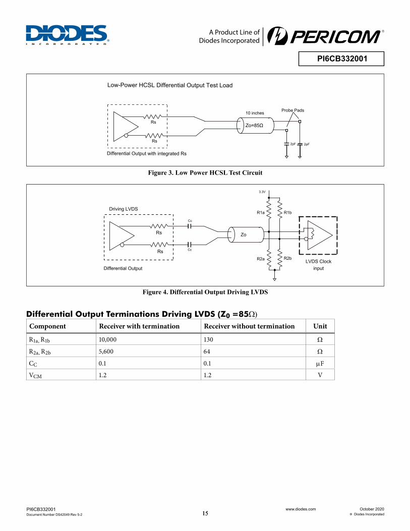
Rs
R
10 inches
Rs
Zo=85Ω
2pF 2pF
Low-Power HCSL Differential Output Test Load
Differential Output with integrated Rs
Probe Pads
Figure 3. Low Power HCSL Test Circuit
R
Zo
Differential Output
Driving LVDS
Cc
Cc
R1a R1b
R2a R2b
3.3V
LVDS Clockinput
Rs
Rs
Figure 4. Differential Output Driving LVDS
Differential Output Terminations Driving LVDS (Z0 =85W)Component Receiver with termination Receiver without termination Unit
R1a, R1b 10,000 130 W
R2a, R2b 5,600 64 W
CC 0.1 0.1 mF
VCM 1.2 1.2 V
1616
A Product Line ofDiodes Incorporated
PI6CB332001
www.diodes.com October 2020 Diodes Incorporated
PI6CB332001 Document Number DS42049 Rev 5-2
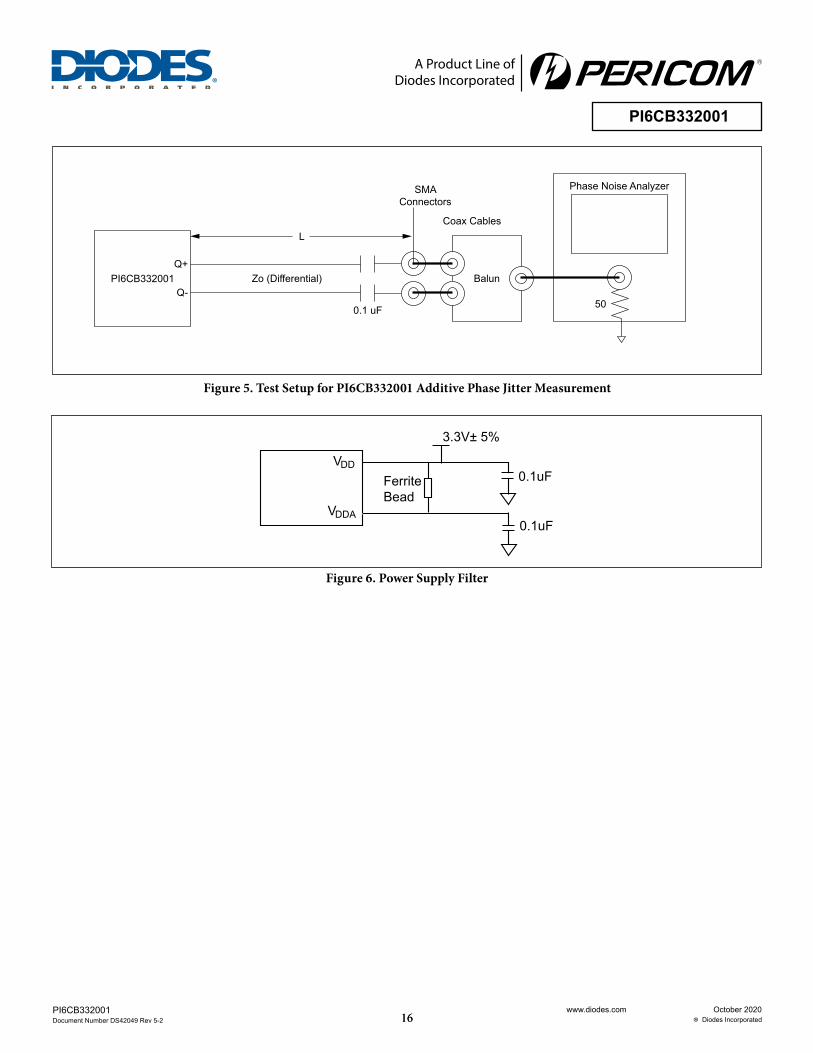
Figure 6. Power Supply Filter
m
0.1uF
0.1uF
3.3V± 5%
VDD
VDDA
FerriteBead
Q+
L
Q-PI6CB332001 Zo (Differential)
0.1 uF
Balun
50
SMAConnectors
Coax Cables
Phase Noise Analyzer
Figure 5. Test Setup for PI6CB332001 Additive Phase Jitter Measurement
1717
A Product Line ofDiodes Incorporated
PI6CB332001
www.diodes.com October 2020 Diodes Incorporated
PI6CB332001 Document Number DS42049 Rev 5-2
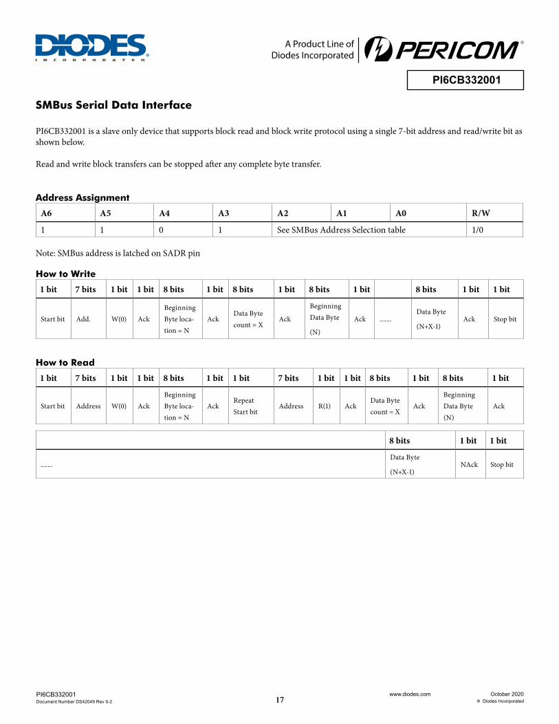
SMBus Serial Data Interface
PI6CB332001 is a slave only device that supports block read and block write protocol using a single 7-bit address and read/write bit as shown below.
Read and write block transfers can be stopped after any complete byte transfer.
Address Assignment
A6 A5 A4 A3 A2 A1 A0 R/W
1 1 0 1 See SMBus Address Selection table 1/0
Note: SMBus address is latched on SADR pin
How to Write
1 bit 7 bits 1 bit 1 bit 8 bits 1 bit 8 bits 1 bit 8 bits 1 bit 8 bits 1 bit 1 bit
Start bit Add. W(0) AckBeginning Byte loca-tion = N
AckData Byte count = X
Ack
Beginning Data Byte
(N)
Ack .......Data Byte
(N+X-1)Ack Stop bit
How to Read
1 bit 7 bits 1 bit 1 bit 8 bits 1 bit 1 bit 7 bits 1 bit 1 bit 8 bits 1 bit 8 bits 1 bit
Start bit Address W(0) AckBeginning Byte loca-tion = N
AckRepeat Start bit
Address R(1) AckData Byte count = X
AckBeginning Data Byte (N)
Ack
8 bits 1 bit 1 bit
.......Data Byte
(N+X-1)NAck Stop bit

1818
A Product Line ofDiodes Incorporated
PI6CB332001
www.diodes.com October 2020 Diodes Incorporated
PI6CB332001 Document Number DS42049 Rev 5-2
Byte 0: Output Enable Register
Bit Control Function Description Type Power Up Condition 0 1
7 Reserved 0
6 Q19_OE Q19 output enable RW 1 Low/Low Enable
5 Q18_OE Q18 output enable RW 1 Low/Low Enable
4 Q17_OE Q17 output enable RW 1 Low/Low Enable
3 Q16_OE Q16 output enable RW 1 Low/Low Enable
2 Reserved 0
1 Reserved 0
0 Reserved 0
Byte 1: Output Enable Register
Bit Control Function Description Type Power Up Condition 0 1
7 Q7_OE Q7 output enable RW 1 Low/Low OE7# control
6 Q6_OE Q6 output enable RW 1 Low/Low OE6# control
5 Q5_OE Q5 output enable RW 1 Low/Low OE5# control
4 Q4_OE Q4 output enable RW 1 Low/Low Enable
3 Q3_OE Q3 output enable RW 1 Low/Low Enable
2 Q2_OE Q2 output enable RW 1 Low/Low Enable
1 Q1_OE Q1 output enable RW 1 Low/Low Enable
0 Q0_OE Q0 output enable RW 1 Low/Low Enable
Byte 2: Output Enable Register
Bit Control Function Description Type Power Up Condition 0 1
7 Q15_OE Q15 output enable RW 1 Low/Low Enable
6 Q14_OE Q14 output enable RW 1 Low/Low Enable
5 Q13_OE Q13 output enable RW 1 Low/Low Enable
4 Q12_OE Q12 output enable RW 1 Low/Low OE12# control
3 Q11_OE Q11 output enable RW 1 Low/Low OE11# control
2 Q10_OE Q10 output enable RW 1 Low/Low OE10# control
1 Q9_OE Q9 output enable RW 1 Low/Low OE9# control
0 Q8_OE Q8 output enable RW 1 Low/Low OE8# control
1919
A Product Line ofDiodes Incorporated
PI6CB332001
www.diodes.com October 2020 Diodes Incorporated
PI6CB332001 Document Number DS42049 Rev 5-2
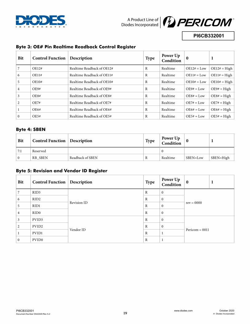
Byte 3: OE# Pin Realtime Readback Control Register
Bit Control Function Description Type Power Up Condition 0 1
7 OE12# Realtime Readback of OE12# R Realtime OE12# = Low OE12# = High
6 OE11# Realtime Readback of OE11# R Realtime OE11# = Low OE11# = High
5 OE10# Realtime Readback of OE10# R Realtime OE10# = Low OE10# = High
4 OE9# Realtime Readback of OE9# R Realtime OE9# = Low OE9# = High
3 OE8# Realtime Readback of OE8# R Realtime OE8# = Low OE8# = High
2 OE7# Realtime Readback of OE7# R Realtime OE7# = Low OE7# = High
1 OE6# Realtime Readback of OE6# R Realtime OE6# = Low OE6# = High
0 OE5# Realtime Readback of OE5# R Realtime OE5# = Low OE5# = High
Byte 4: SBEN
Bit Control Function Description Type Power Up Condition 0 1
7:1 Reserved 0
0 RB_SBEN Readback of SBEN R Realtime SBEN=Low SBEN=High
Byte 5: Revision and Vendor ID Register
Bit Control Function Description Type Power Up Condition 0 1
7 RID3
Revision ID
R 0
rev = 00006 RID2 R 0
5 RID1 R 0
4 RID0 R 0
3 PVID3
Vendor ID
R 0
Pericom = 00112 PVID2 R 0
1 PVID1 R 1
0 PVID0 R 1

2020
A Product Line ofDiodes Incorporated
PI6CB332001
www.diodes.com October 2020 Diodes Incorporated
PI6CB332001 Document Number DS42049 Rev 5-2
Byte 6: Device Type/Device ID Register
Bit Control Function Description Type Power Up Condition 0 1
7 DID7
Device ID
R 0
6 DID6 R 1
5 DID5 R 0
4 DID4 R 0
3 DID3 R 1
2 DID2 R 0
1 DID1 R 0
0 DID0 R 0
Byte 7: Byte Count Register
Bit Control Function Description Type Power Up Condition 0 1
7 Reserved 0
6 Reserved 0
5 Reserved 0
4 BC4
Byte count programming
RW 0
Writing to this register will configure how many bytes will be read back, default is 8 bytes
3 BC3 RW 1
2 BC2 RW 0
1 BC1 RW 0
0 BC0 RW 0
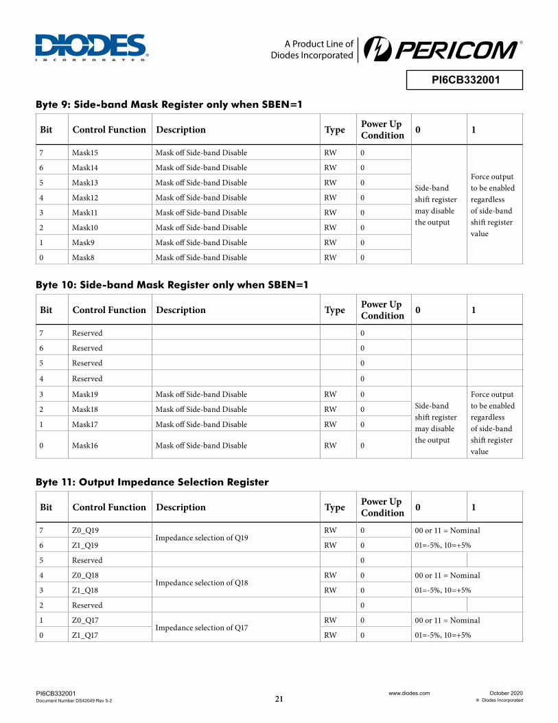
Byte 8: Side-band Mask Register only when SBEN=1
Bit Control Function Description Type Power Up Condition 0 1
7 Mask7 Mask off Side-band Disable RW 0
Side-band shift register may disable the output
Force output to be enabled regardless of side-band shift register value
6 Mask6 Mask off Side-band Disable RW 0
5 Mask5 Mask off Side-band Disable RW 0
4 Mask4 Mask off Side-band Disable RW 0
3 Mask3 Mask off Side-band Disable RW 0
2 Mask2 Mask off Side-band Disable RW 0
1 Mask1 Mask off Side-band Disable RW 0
0 Mask0 Mask off Side-band Disable RW 0
2121
A Product Line ofDiodes Incorporated
PI6CB332001
www.diodes.com October 2020 Diodes Incorporated
PI6CB332001 Document Number DS42049 Rev 5-2
Byte 10: Side-band Mask Register only when SBEN=1
Bit Control Function Description Type Power Up Condition 0 1
7 Reserved 0
6 Reserved 0
5 Reserved 0
4 Reserved 0
3 Mask19 Mask off Side-band Disable RW 0Side-band shift register may disable the output
Force output to be enabled regardless of side-band shift register value
2 Mask18 Mask off Side-band Disable RW 0
1 Mask17 Mask off Side-band Disable RW 0
0 Mask16 Mask off Side-band Disable RW 0
Byte 11: Output Impedance Selection Register
Bit Control Function Description Type Power Up Condition 0 1
7 Z0_Q19Impedance selection of Q19
RW 0 00 or 11 = Nominal
01=-5%, 10=+5%6 Z1_Q19 RW 0
5 Reserved 0
4 Z0_Q18Impedance selection of Q18
RW 0 00 or 11 = Nominal
01=-5%, 10=+5%3 Z1_Q18 RW 0
2 Reserved 0
1 Z0_Q17Impedance selection of Q17
RW 0 00 or 11 = Nominal
01=-5%, 10=+5%0 Z1_Q17 RW 0
Byte 9: Side-band Mask Register only when SBEN=1
Bit Control Function Description Type Power Up Condition 0 1
7 Mask15 Mask off Side-band Disable RW 0
Side-band shift register may disable the output
Force output to be enabled regardless of side-band shift register value
6 Mask14 Mask off Side-band Disable RW 0
5 Mask13 Mask off Side-band Disable RW 0
4 Mask12 Mask off Side-band Disable RW 0
3 Mask11 Mask off Side-band Disable RW 0
2 Mask10 Mask off Side-band Disable RW 0
1 Mask9 Mask off Side-band Disable RW 0
0 Mask8 Mask off Side-band Disable RW 0
2222
A Product Line ofDiodes Incorporated
PI6CB332001
www.diodes.com October 2020 Diodes Incorporated
PI6CB332001 Document Number DS42049 Rev 5-2
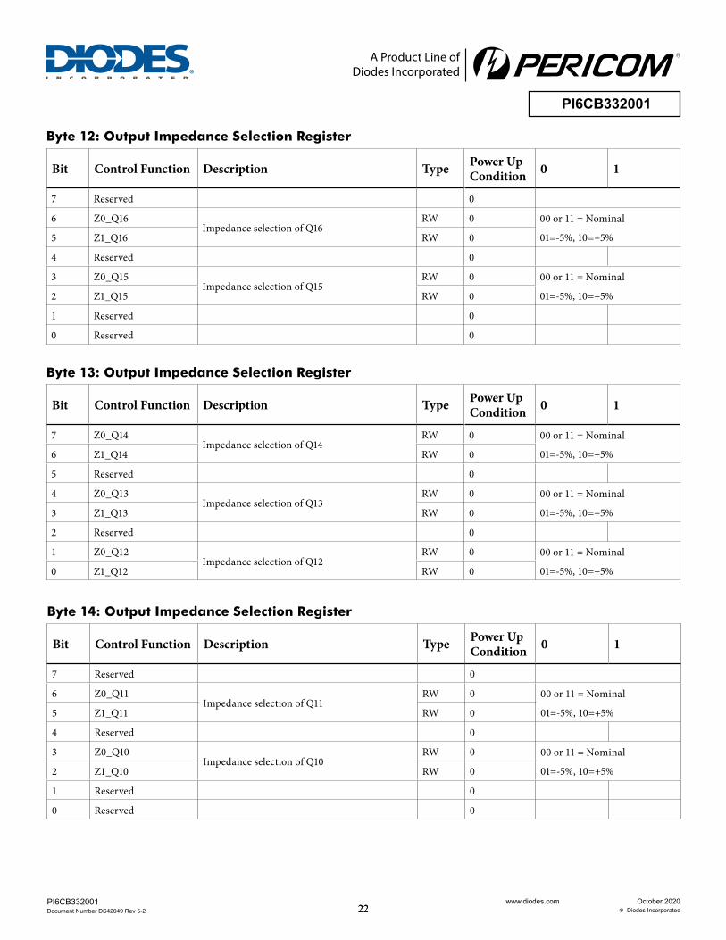
Byte 12: Output Impedance Selection Register
Bit Control Function Description Type Power Up Condition 0 1
7 Reserved 0
6 Z0_Q16Impedance selection of Q16
RW 0 00 or 11 = Nominal
01=-5%, 10=+5%5 Z1_Q16 RW 0
4 Reserved 0
3 Z0_Q15Impedance selection of Q15
RW 0 00 or 11 = Nominal
01=-5%, 10=+5%2 Z1_Q15 RW 0
1 Reserved 0
0 Reserved 0
Byte 13: Output Impedance Selection Register
Bit Control Function Description Type Power Up Condition 0 1
7 Z0_Q14Impedance selection of Q14
RW 0 00 or 11 = Nominal
01=-5%, 10=+5%6 Z1_Q14 RW 0
5 Reserved 0
4 Z0_Q13Impedance selection of Q13
RW 0 00 or 11 = Nominal
01=-5%, 10=+5%3 Z1_Q13 RW 0
2 Reserved 0
1 Z0_Q12Impedance selection of Q12
RW 0 00 or 11 = Nominal
01=-5%, 10=+5%0 Z1_Q12 RW 0
Byte 14: Output Impedance Selection Register
Bit Control Function Description Type Power Up Condition 0 1
7 Reserved 0
6 Z0_Q11Impedance selection of Q11
RW 0 00 or 11 = Nominal
01=-5%, 10=+5%5 Z1_Q11 RW 0
4 Reserved 0
3 Z0_Q10Impedance selection of Q10
RW 0 00 or 11 = Nominal
01=-5%, 10=+5%2 Z1_Q10 RW 0
1 Reserved 0
0 Reserved 0
2323
A Product Line ofDiodes Incorporated
PI6CB332001
www.diodes.com October 2020 Diodes Incorporated
PI6CB332001 Document Number DS42049 Rev 5-2
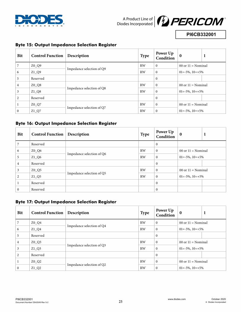
Byte 15: Output Impedance Selection Register
Bit Control Function Description Type Power Up Condition 0 1
7 Z0_Q9Impedance selection of Q9
RW 0 00 or 11 = Nominal
01=-5%, 10=+5%6 Z1_Q9 RW 0
5 Reserved 0
4 Z0_Q8Impedance selection of Q8
RW 0 00 or 11 = Nominal
01=-5%, 10=+5%3 Z1_Q8 RW 0
2 Reserved 0
1 Z0_Q7Impedance selection of Q7
RW 0 00 or 11 = Nominal
01=-5%, 10=+5%0 Z1_Q7 RW 0
Byte 16: Output Impedance Selection Register
Bit Control Function Description Type Power Up Condition 0 1
7 Reserved 0
6 Z0_Q6Impedance selection of Q6
RW 0 00 or 11 = Nominal
01=-5%, 10=+5%5 Z1_Q6 RW 0
4 Reserved 0
3 Z0_Q5Impedance selection of Q5
RW 0 00 or 11 = Nominal
01=-5%, 10=+5%2 Z1_Q5 RW 0
1 Reserved 0
0 Reserved 0
Byte 17: Output Impedance Selection Register
Bit Control Function Description Type Power Up Condition 0 1
7 Z0_Q4Impedance selection of Q4
RW 0 00 or 11 = Nominal
01=-5%, 10=+5%6 Z1_Q4 RW 0
5 Reserved 0
4 Z0_Q3Impedance selection of Q3
RW 0 00 or 11 = Nominal
01=-5%, 10=+5%3 Z1_Q3 RW 0
2 Reserved 0
1 Z0_Q2Impedance selection of Q2
RW 0 00 or 11 = Nominal
01=-5%, 10=+5%0 Z1_Q2 RW 0
2424
A Product Line ofDiodes Incorporated
PI6CB332001
www.diodes.com October 2020 Diodes Incorporated
PI6CB332001 Document Number DS42049 Rev 5-2
Byte 18: Output Impedance Selection Register
Bit Control Function Description Type Power Up Condition 0 1
7 Reserved 0
6 Z0_Q1Impedance selection of Q1
RW 0 00 or 11 = Nominal
01=-5%, 10=+5%5 Z1_Q1 RW 0
4 Reserved 0
3 Z0_Q0Impedance selection of Q0
RW 0 00 or 11 = Nominal
01=-5%, 10=+5%2 Z1_Q0 RW 0
1 Reserved 0
0 Reserved 0
Byte 20: Stop State Configuration Register
Bit Control Function Description Type Power Up Condition 0 1
7 VSW[2]
Global differential output swing control
RW 1 Default=750mV
0.3V-1.0V
100mV/Step
6 VSW[1] RW 0
5 VSW[0] RW 1
4 Reserved 0
3 Reserved 0
2 Reserved 1
1 STOPST[1]Differential Stop Mode State
RW 0 00=Low/Low; 10=High/Low
01=HiZ/HiZ; 11=Low/High0 STOPST[0] RW 0
Byte 19: Reserve
Byte 21: Power Down Restore Configuration Register
Bit Control Function Description Type Power Up Condition 0 1
7 Reserved 0
6 Reserved 0
5 Reserved 0
4 Reserved 0
3 PD_RESTORE# Save configuration in power down mode RW 1 Config cleared Config saved
2 Reserved 0
1 Reserved 0
0 Reserved 0

2525
A Product Line ofDiodes Incorporated
PI6CB332001
www.diodes.com October 2020 Diodes Incorporated
PI6CB332001 Document Number DS42049 Rev 5-2
Phase Noise Plots100MHz input phase noise vs output phase noise. Additive jitter1 67fs.
156.25MHz input phase noise vs output phase noise. Additive jitter1 51fs.
Note:
1. Additive jitter RMS value is calculated by the following equation = SQRT [(total jitter)*2 - (input jitter)*2]
2626
A Product Line ofDiodes Incorporated
PI6CB332001
www.diodes.com October 2020 Diodes Incorporated
PI6CB332001 Document Number DS42049 Rev 5-2
Part Marking
2727
A Product Line ofDiodes Incorporated
PI6CB332001
www.diodes.com October 2020 Diodes Incorporated
PI6CB332001 Document Number DS42049 Rev 5-2
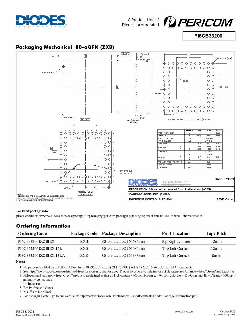
Ordering InformationOrdering Code Package Code Package Description Pin 1 Location Tape Pitch
PI6CB332001ZXBIEX ZXB 80-contact, aQFN 6x6mm Top Right Corner 12mm
PI6CB332001ZXBIEX-13R ZXB 80-contact, aQFN 6x6mm Top Left Corner 12mm
PI6CB332001ZXBIEX-13RA ZXB 80-contact, aQFN 6x6mm Top Left Corner 8mm
Packaging Mechanical: 80-aQFN (ZXB)
For latest package info. please check: http://www.diodes.com/design/support/packaging/pericom-packaging/packaging-mechanicals-and-thermal-characteristics/
Notes:
1. No purposely added lead. Fully EU Directive 2002/95/EC (RoHS), 2011/65/EU (RoHS 2) & 2015/863/EU (RoHS 3) compliant. 2. See https://www.diodes.com/quality/lead-free/ for more information about Diodes Incorporated’s definitions of Halogen- and Antimony-free, "Green" and Lead-free. 3. Halogen- and Antimony-free "Green” products are defined as those which contain <900ppm bromine, <900ppm chlorine (<1500ppm total Br + Cl) and <1000ppm
antimony compounds.4. I = Industrial5. E = Pb-free and Green6. X suffix = Tape/Reel7. For packaging detail, go to our website at: https://www.diodes.com/assets/MediaList-Attachments/Diodes-Package-Information.pdf

2828
A Product Line ofDiodes Incorporated
PI6CB332001
www.diodes.com October 2020 Diodes Incorporated
PI6CB332001 Document Number DS42049 Rev 5-2
IMPORTANT NOTICE
DIODES INCORPORATED MAKES NO WARRANTY OF ANY KIND, EXPRESS OR IMPLIED, WITH REGARDS TO THIS DOCUMENT, INCLUDING, BUT NOT LIMITED TO, THE IMPLIED WARRANTIES OF MERCHANTABILITY AND FITNESS FOR A PARTICULAR PURPOSE (AND THEIR EQUIVALENTS UNDER THE LAWS OF ANY JURISDICTION).
Diodes Incorporated and its subsidiaries reserve the right to make modifications, enhancements, improvements, corrections or other changes without further no-tice to this document and any product described herein. Diodes Incorporated does not assume any liability arising out of the application or use of this document or any product described herein; neither does Diodes Incorporated convey any license under its patent or trademark rights, nor the rights of others. Any Customer or user of this document or products described herein in such applications shall assume all risks of such use and will agree to hold Diodes Incorporated and all the companies whose products are represented on Diodes Incorporated website, harmless against all damages.
Diodes Incorporated does not warrant or accept any liability whatsoever in respect of any products purchased through unauthorized sales channel.
Should Customers purchase or use Diodes Incorporated products for any unintended or unauthorized application, Customers shall indemnify and hold Diodes Incorporated and its representatives harmless against all claims, damages, expenses, and attorney fees arising out of, directly or indirectly, any claim of personal injury or death associated with such unintended or unauthorized application.
Products described herein may be covered by one or more United States, international or foreign patents pending. Product names and markings noted herein may also be covered by one or more United States, international or foreign trademarks.
This document is written in English but may be translated into multiple languages for reference. Only the English version of this document is the final and determi-native format released by Diodes Incorporated.
LIFE SUPPORT
Diodes Incorporated products are specifically not authorized for use as critical components in life support devices or systems without the express written approval of the Chief Executive Officer of Diodes Incorporated. As used herein:
A. Life support devices or systems are devices or systems which:
1. are intended to implant into the body, or
2. support or sustain life and whose failure to perform when properly used in accordance with instructions for use provided in the labeling can be reasonably expected to result in significant injury to the user.
B. A critical component is any component in a life support device or system whose failure to perform can be reasonably expected to cause the
failure of the life support device or to affect its safety or effectiveness.
Customers represent that they have all necessary expertise in the safety and regulatory ramifications of their life support devices or systems, and acknowledge and agree that they are solely responsible for all legal, regulatory and safety-related requirements concerning their products and any use of Diodes Incorporated products in such safety-critical, life support devices or systems, notwithstanding any devices- or systems-related information or support that may be provided by Diodes Incorporated. Further, Customers must fully indemnify Diodes Incorporated and its representatives against any damages arising out of the use of Diodes Incorporated products in such safety-critical, life support devices or systems.
Copyright © 2020, Diodes Incorporated
www.diodes.com