fc3g2 training manual -...
TRANSCRIPT

1 Training Manual FC3G2 Chassis
FILE NO.
COLOUR TELEVISIONTRAINING MANUAL
Chassis Series FC3G2
CIRCUIT DESCRIPTION BLOCK DIAGRAM OF ICs TROUBLE SHOOTING
REFERENCE NO.XXXXXX

2 Training Manual FC3G2 Chassis
Table of Contents Part 1 Chassis Description ..................................................................................... 3 1. Chassis Summary ....................................................................................................... 3 2. CPU (System Control) ................................................................................................. 4 2-1 A-D Key Identification Circuit. ..................................................................................... 8 2-2 Memory Option ......................................................................................................... 10 2-3 Power / stand-by circuit. ............................................................................................ 13 2-4 Protection circuit........................................................................................................ 13 2-5 AFT............................................................................................................................ 14 2-6 Horizontal/Vertical pulse input................................................................................... 18 2-7 Service mode ............................................................................................................ 19 3. IF /Video/Chroma/Deflection .................................................................................... 22 3-1 IF stage...................................................................................................................... 22 3-2 Video/Chroma stage.................................................................................................. 22 3-3 Deflection stage......................................................................................................... 22 4. Audio Output.............................................................................................................. 23 5. Vertical........................................................................................................................ 24 6. Horizontal .................................................................................................................. 24 7. Power Consumption Saving Circuit. ....................................................................... 25 Part 2 Block Diagram of ICs ................................................................................. 28 1. LA76818A (IF/VIDEO/CHROMA/DEFLECTION)....................................................... 28 2. LA78040N (VERTICAL OUTPUT).............................................................................. 30 3. AN17820B (AUDIO OUTPUT) .................................................................................... 30 4. LA7642NM (SECAM DECODER)............................................................................... 31 5. 24LC16B/P (IC MEMORY) ......................................................................................... 31 Part 3 Trouble shooting Chart ............................................................................. 32 Trouble Shooting Chart Startpoint symptom: Dead .............................................. 33 Trouble Shooting Chart Starpoint symptom: No picture-no sound ....................... 36 Trouble Shooting Chart Starpoint symptom: No picture-sound OK...................... 38 Trouble Shooting Chart Starpoint symptom: No sound-picture OK...................... 39 Trouble Shooting Chart Starpoint symptom: No color & color NG........................ 40 Trouble Shooting Chart Startpoint symptom: No vertical deflection ..................... 41 Trouble Shooting Chart Startpoint symptom: No on-screen display..................... 42 Short – Open Test Report ............................................................................................... 43

3 Training Manual FC3G2 Chassis
Part 1 Chassis Description 1. Chassis Summary
The following figure shows a basic block diagram of the FC3G2 chassis. This chassis is constructed by the folowing ICs : AN17820B, IC001, for the audio output circuit LA76818A, IC201, for the IF, video, chroma de-modulation and deflection circuit LA7642NM-TLM-E, IC281, for the SECAM decoder circuit. NJW1142M, IC3701, for audio processor LA78041, IC501, for the vertical deflection output circuit LC863448W-52F1-TLM, IC801, for the CPU (system control unit) of FC3G2 AT24C16A-10PI-2.7, IC802, for the control memory IC. MM1188XS & TC4053BF-TP1, IC1401 & IC 1501, for video selector.
Figure of FC3G2 block diagram
A1901ARC
RECEIVER
D1910LED
FRONT CONTROL
KEYS
SW1901 ~SW1906
KEY-IN
POWER
ON-TIMER
RC-IN
S-VIDEO IN (FROM S-TERMINAL)
IC001AUDIO AMP.
SP902
SP901
R-OUT
L-OUT
12
2
8
6
R
L
REARMONITOR
OUTTERMINAL
REARAV1
INPUTTERMINAL
FRONTAV2
INPUTTERMINAL
V
L
R
V
L
R
V
L
R
VIDEO MONITOR OUT
AUDIO MONITOR OUT(LEFT)
AUDIO MONITOR OUT(RIGHT)
AV1 L-IN
AV1 R-IN
AV2 R-IN
AV2 L-IN
AV2
VIDE
O IN
AV1
VIDE
O IN
S-TERMINALC-IN
Y-IN
9
1
6
7
38
4+
AV2/S-INPUTAV1/AV2
(FROM CPU PIN-25)C-INY-IN
SDA/
SCL
(FRO
M C
PU)
5
26
2
29
3
28
10
21
(L-TV-L)1/30
AUDIOCONTROL/
SURROUND
IC3701
R-OUT
TV-AUDIO
L-OU
T
VIDEOOUT (TV)
VIDEO-INY-IN
IC201IF/VIDEO/CHROMA
11/12
14
15
16
46
42
1
44
5/6
19
20
21
23
27
TVAUDIOOUT
INT.VIDEO IN(C-IN)
VIDEO MONITOR OUT
R-OUT
G-OUT
B-OUT
VERT.OUT
HORIZ.OUT
Q431H-DRIVE
IC1501VIDEO SELECTOR
AV IN
TV IN
TV IN
AV,Y IN
AV-IN
Y-IN
2
1
5
3
13
12
11 9 10
14
4
15
TV/AV (FROM CPU PIN-24)S-INPUT
28
32
31
12
11
3
4
19
20
21
1/2
24
26
IC801CPU
IC802EEPROM
SDA
SCL
OSD R-OUT
OSD G-OUT
OSD B-OUT
SDA/SCL
TV/AV OUT
AV1/AV2 OUT
5
6
SDA/SCL
A101TUNER
SAWFILTER
X161
IF IN
T431H-DRIVETRANS.
Q432H-OUT
1 5IC501VERT./DEF.
CRT UNIT
IC701TRIPLE VIDEOOUTPUT AMP.
R
G
B
R
G
B
1
2
3 7
8
9
HEATER
L902DY
HV
T471FBT
FOCUS
SCREEN
HV
CRT
AV-OUTY-OUT
TV/AV OUTY-OUT
MONITOROUT
POWER SUPPLY CIRCUIT
140V
24V
11V
9V
MAIN SOUND AMP.
HORIZ. DEF.
VERT. DEF.
FBT
TUNER36V
9V
5V
IC201, AUDIO CTL.
CPU, EEPROM
IC1401VIDEO
SELECTOR
AV OUT
R-IN
G-IN
B-IN
13/14
PCCCIRCUIT
Q461-Q462

4 Training Manual FC3G2 Chassis
2. CPU (System Control)
The following firgure shows a block diagram of the CPU peripheral circuit. CPU that use for FC3G2 is AC5G2 CPU.
TERMINAL ASSIGNMENT (AC5G2 CPU)
LC863448W-52F1-TLM (ROM:48Kbytes)
BUS SDA 1 P10/SDA0 * P03 36 Status input(factory)
V/C IC (Low:factory mode) BUS SCL 2 P11/SCLK0 P02 35 ACK output(factory)
(Low:factory mode) IIC SDA 3 P12/SDA1 * P01 34 BASS output & Woofer Output
EEPROM IIC SCL 4 P13/SCLK1 P00 33 VIF-M output
(High:NTSC,Low:other) Vss(GND) 5 Vss P17 32 ON timer LED on/off output
(Low:Timer on) CPU OSC input 6 XT1 P16/PWM3 31 Power on/off output
(X’tal 32.768KHz) (High:on) CPU OSC output 7 XT2 P15/PWM2 30 Volume PWM output
VDD(+5V) 8 VDD P14/PWM1 29 Sound Mute output
(High:Mute ON) SECAM Killer Input 9 P04/AN4 P73/INT3 28 remote control signal input
AFT signal input 10 P05/AN5 P72/INT2 27 Power failure input
S-Video input (Low: S-in) 11 P06/AN6 * P71/INT1 26 TV/AV1/AV2/AV3
option output panel key input 12 P07/AN7 P70/INT0 25 50/60 output (Low:60Hz)
(PAL:50Hz, NTSC:60Hz) RESET input 13 RESET P32 24 TV/AV1/AV2/AV3
option output Filter for PLL 14 FILT P31 23 L/R or L/L
(Connect to ground through CR) CV input(no use=open) 15 CVIN BLNK 22 OSD Blanking signal output
Bilingual output 16 P30 B 21 OSD Blue signal output
(Low:S-1,High:S-2) V-sync signal input 17 VS G 20 OSD Green signal output
H-sync signal input 18 HS R 19 OSD Red signal output
NOTE : * N-ch.open drain output (Vout max.+5V)

5 Training Manual FC3G2 Chassis
The following table shows pin description of CPU. Port Description Table
PIN Port Name
Use
I/O
Output Structure
Input p-up R
Reset Notes
1 SDA0 IIC DATA I/O Nch-OD No Hz BUS IC 2 SCL0 IIC CLOCK O Nch-OD No Hz BUS IC 3 SDA1 BUS DATA I/O Nch-OD No Hz EEPROM 4 SCL1 BUS CLOCK O Nch-OD No Hz EEPROM 5 VSS GND - - 6 XT1 X’tal input I - - 32.768KHz 7 XT2 X’tal output O - - 8 VDD +5V I - - 9 AN4 SECAM Killer input I Nch-OD No - High: SECAM 10 AN5 AFT IN I - No - AFT signal 11 AN6 S-Terminal input I Nch-OD No - Low: S-In 12 AN7 Panel keys input I - No - Panel keys 13 RES RESET I - - Reset:Low 14 FILT FILTER for PLL O - - 15 CVIN CV input I - - (Composite Video) 16 P30 Bilingual output O - yes - 17 VS V-sync signal input I - - Active Low 18 HS H-sync signal input I - - Active Low 19 R OSD Red output O C-MOS L Active High 20 G OSD Green output O C-MOS L Active High 21 B OSD Blue output O C-MOS L Active High 22 BLNK OSD Blanking output O C-MOS L Active High 23 P31 L/R or L/L output O C-MOS Hz Low:L/R 24 P32 TV/AV123 output O C-MOS yes Hz Option TV/AV1/AV2/AV3 25 P70 50/60Hz output O C-MOS No Hz Low:60Hz 26 P71 TV/AV123 output O C-MOS No Hz Option TV/AV1/AV2/AV3 27 P72 Power failure input I Nch-OD No Hz Low:fail 28 P73 Remotecontrol signal I Nch-OD No Hz Active High 29 P14 Sound Mute output O C-MOS No Hz High:Mute on 30 PWM2 Volume PWM output O C-MOS No Hz 31 P16 Power on/off output O C-MOS No Hz High:Power on 32 P17 On timer LED output O C-MOS No Hz Low:timer on 33 P00 VIF-M O C-MOS No Hz High:NTSC 34 P01 Bass expander I/O Nch-OD No Hz High:BASS on 35 P02 ACK O C-MOS No Hz Factory:Low 36 P03 Status input I Nch-OD No Hz Factory:Low
Note : Hz = High impedance

6 Training Manual FC3G2 Chassis
≪CPU Specification outline≫ This tuning system is equipped with the F/S tuning system for AC5G2 chassis. It has the following specification. (1) Monaural, Simple AV Stereo & AV stereo Function (2) Maximum 256 Positions. Optional 100 or 256 Position (EPROM : 16k bit for 256
Pos) ① The direct tuning function can be work by pressing “[0]~[9] key” and “[-/--] key” ② The sequential tuning function can be work by pressing [POS -] and [POS +]
key ③ The alternate tuning function can be work by [Alt] key
(3) PRESET function [Automatic Tuning/Semi-Auto Tuning/Manual Tuning] Plug & Play function (4) Channel Swap function & Channel Skip function (5) Bilingual system (6) Option system
A. Memory options ① Color system selection : Five kinds ② Sif system selection : Six kinds ③ AV input option : AV only or AV1/AV2 or AV1/AV2/AV3 ④ BASS EXPANDER selection : with or without ⑤ SURROUND selection : with or without
B. Special function (Dealer) options ① Tuning Lock : on or off ② Volume Lock : on or off ③ AV start : on or off ④ Music mode : on or off
(7) Digital AFT (Auto Fine Tuning) function (8) Front controls
[Volume Up] / [Volume Down] [Programme Up] / [Programme Down] [TV/AV] Selector
(9) OSD is a multi-color display (the R/G/B output). (10) OFF timer function(30/60/90/120 minutes) (11) ON timer function (10 minutes ~ 24 hours)
7 Training Manual FC3G2 Chassis
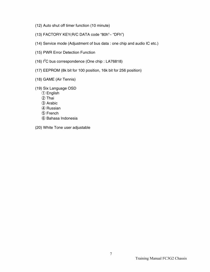
(12) Auto shut off timer function (10 minute) (13) FACTORY KEY(R/C DATA code “80h”~ “DFh”) (14) Service mode (Adjustment of bus data : one chip and audio IC etc.) (15) PWR Error Detection Function (16) I2C bus correspondence (One chip : LA76818) (17) EEPROM (8k bit for 100 position, 16k bit for 256 position) (18) GAME (Air Tennis) (19) Six Language OSD ① English ② Thai ③ Arabic ④ Russian ⑤ French ⑥ Bahasa Indonesia (20) White Tone user adjustable

8 Training Manual FC3G2 Chassis
2-1 A-D Key Identification Circuit. The key identification circuit used in this chassis uses a switched resistive ladder network in a A-D conversion circuit to generate and send a voltage to the CPU when a key pressed. The CPU uses this voltage to determine which key was pressed. This resistive circuit eliminates the need for encoder/decoder devices, simplifying design and adding to the reliability of the TV. The table shows the voltage input to CPU pin 12, when a given key pressed. Front Control Key Input
1) Action Front panel SW is decied by the input voltage of A/D port (12pin).
2) Circuit * S-terminal-less model key port 12PIN
* S-terminal model key port (12PIN)
R12K
R5.6K
R3.9K
R2.2K
R1.8K
R1.0K
R10K
CPU 12 PINKEY SW INPUT
5V
K1K2K3K4K5K6
K1K2K3K4K5
R12K
R5.5K
R3.9K
R2.2K
R1.8K
R1.0K
R10K
CPU 12 PINKEY SW INPUT
5V
K6 R27K

9 Training Manual FC3G2 Chassis
* Key Table Key VOL. Range(Vcc ratio) (V) ΣR FUNCTION
K6 109/128Vcc ≦ K6 < 127/128Vcc 4.26~ Vcc 1.0K TV/AV
K5 93/128Vcc ≦ K5 < 109/128Vcc 3.63~4.26 2.8K MENU K4 77/128Vcc ≦ K4 < 93/128Vcc 3.01~3.63 5.0K VOLUME - K3 61/128Vcc ≦ K3 < 77/128Vcc 2.38~3.01 8.9K VOLUME + K2 45/128Vcc ≦ K2 < 61/128Vcc 1.76~2.38 14.5K POSITION - K1 29/128Vcc ≦ K1 < 45/128Vcc 1.13~1.76 26.5K POSITION + OFF 2 13/128Vcc ≦ OFF< 29/128Vcc 0.51~1.13 53.5K OFF (S-Available) OFF 1 OFF < 13/128Vcc <0.51 OPEN OFF (S-N/A) * Mechanism SW is used for K1-7. 3. Action * The Key scan will be performed every 20 msec. It judges whether the key was pressed or not . * When the Key signal is match within two consecutive time at intervals of 20msec , the key is decided. * The Key scan priority is K6 -> K1. * The high priority key has pushed, other keys cannot operate. 4. S-input Option
* The “KEY OFF” voltage distinguishes availability of S-Terminal. * The “KEY OFF” voltage range is divided into two kinds.
1. When KEY OFF voltage is less than 0.51V, it is decide as an S-terminal-less model.
2. When KEY OFF voltage is from 0.51 to 1.13V, it is decide as S-terminal model. <The option selection method >
* Judgment is always (20 ms) performed. (agrement with two consecutive time * This option is decided only in KEY OFF. An option does not change when
K1 ~ K6 was inputted.
Bus data of LA76818 VIDEO
SW OFF 1
(S term less) OFF 2
(S term) Address TV AV TV AV
14H DAO 0 1 1 1
10 Training Manual FC3G2 Chassis
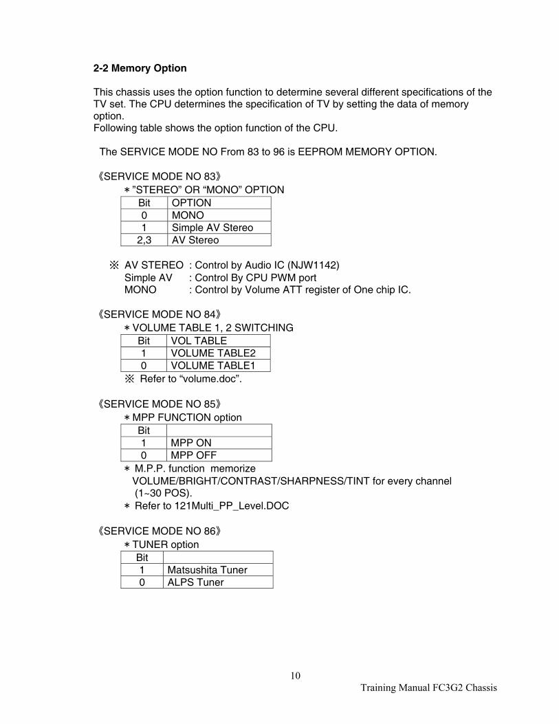
2-2 Memory Option This chassis uses the option function to determine several different specifications of the TV set. The CPU determines the specification of TV by setting the data of memory option. Following table shows the option function of the CPU.
The SERVICE MODE NO From 83 to 96 is EEPROM MEMORY OPTION. 《SERVICE MODE NO 83》
* ”STEREO” OR “MONO” OPTION Bit OPTION 0 MONO 1 Simple AV Stereo
2,3 AV Stereo
※ AV STEREO : Control by Audio IC (NJW1142) Simple AV : Control By CPU PWM port
MONO : Control by Volume ATT register of One chip IC. 《SERVICE MODE NO 84》
* VOLUME TABLE 1, 2 SWITCHING Bit VOL TABLE 1 VOLUME TABLE2 0 VOLUME TABLE1
※ Refer to “volume.doc”. 《SERVICE MODE NO 85》
* MPP FUNCTION option Bit 1 MPP ON 0 MPP OFF
* M.P.P. function memorize VOLUME/BRIGHT/CONTRAST/SHARPNESS/TINT for every channel
(1~30 POS). * Refer to 121Multi_PP_Level.DOC
《SERVICE MODE NO 86》
* TUNER option Bit 1 Matsushita Tuner 0 ALPS Tuner

11 Training Manual FC3G2 Chassis
《SERVICE MODE NO 87》 * AV1, AV2, AV3 Option Bit
0 TV→AV→TV 1 TV→AV1→AV2→TV
2-3 TV→AV1→AV2→AV3→TV 《SERVICE MODE NO 91》 《Description》 * A color system option is changed by a setup in Service Mode No. 91 OPT COL. * A color system option is shown below. There are five kinds of color systems. * COLOR SYSTEM OPTIONS Tabel SVS
data OPTION TV AV
0,1 NO SYSTEM (No Display) PAL only same as the TV MODE. 2 VMT SYSTEM (No Display) PAL + NTSC only AUTO→PAL→NTSC4.43→NTSC 3 CHINA,
INDONESIA AUTO→PAL→NTSC4.43→NTSC same as the TV MODE.
4 3 SYSTEM AUTO→PAL→SECAM→NTSC4.43 same as the TV MODE. 5,6,7 MULTI
SYSTEM AUTO→PAL→SECAM→NTSC4.43→NTSC same as the TV MODE.
《The option selection method》 * An option is changed by Service Mode NO. 91 OPT COL. * The Option check will be carry out on RESET START. * A judgment is performed only once after RESET START. 《SERVICE MODE NO 92》 《Description》 * A SIF system option is changed by Service Mode. * A SIF system option is shown below. There are six kinds of SIF systems. * The bilingual operation differs from the other SIF system option
* SIF SYSTEM OPTIONS SVS
Data OPTION BG (5.5M) D/K (6.5M) I (6.0M) M (4.5M)
0,1,7 NO SYSTEM (BG<5.5>) No display --- --- --- 2 BILINGUAL SYSTEM --- --- (S-1) (S-2)
3 SYSTEM A (S-1) (S-3) (S-2) (S-4) 4 SYSTEM B (S-1) --- --- (S-2) 5 SYSTEM C (S-1) (S-2) --- ---
6 SYSTEM D (S-1) (S-2) (S-3) ※Bilingual specification is displayed as S-1 and S-2. The other modes, each SIF system name is displayed.

12 Training Manual FC3G2 Chassis
《The option selection method》 * An option is changed by Service Mode Data No.92 OPT SIF * The voltage is read in a RESET START after operation. * This judgment operation carry out only a RESET START. 《SERVICE MODE NO 93》
* BASS EXPANDER FUNCTION option Bit Display 0 No Display 1 “BASS” 2 “BASS EXPANDER” 3 “WOOFER”
* If Bass Exp Option is ‘0’ on MONO and Simple AV mode then there will be No AUDIO
Menu on MAIN Menu * This function is available only when using Audio Control IC. * In AV Stereo Mode While BASS EXPANDER ON, AUDIO IC of Bass/Treble DATA is
set as : Bass : +10 dB, Treble : +6 dB * In MONO & Simple AV Stereo Mode if BASS EXPANDER ON, Pin 34 will be “High” 《SERVICE MODE NO 94》
* SURROUND option Bit 1 Surround 0 No Surround
《SERVICE MODE NO 95》
* SUB - BASS/TREBLE adjustment of Audio Control IC (NJW1142) Bit 0 BASS TREBLE Gain –3 db 1 BASS TREBLE Gain 0 db
2,3 BASS TREBLE Gain +3 db * This function available only when using Audio Control IC.
《SERVICE MODE NO 96》
* AGC setting Audio Control IC (NJW1142) Bit 0 AGC OFF 1 AGC ON Level= 600 Mv 2 AGC ON Level= 500 mV 3 AGC ON Level= 300 mV
* This function available only when using Audio Control IC

13 Training Manual FC3G2 Chassis
2-3 Power On/ Stand-by circuit. Power on / stand-by The power on/stand-by signal is output from pin 31 of the CPU. When the stand-by mode is selected the voltage of pin 31 changes from Hi(5V) to Low(0V) to turn off Q681and Q652. Q652 turning off causes Q653 and Q654 to turn off. +24V supply for vertical and horizontal output circuit, +9V supply for IF/VIDEO/Chroma circuit and +5V for tuner circuit are all cut off, resulting in the TV set going into the stand-by mode. When the TV is switched back into the power on mode, Q681 and Q652 are turned on and the relevant voltage are supplied back to each circuit.
2-4 Protection circuit This chassis employs two kinds of protection circuit, one controlled by software through the CPU and the other by hardware. . Protection circuit (software) The protection circuit is provided to disable the operation of the TV set in case of a circuit malfunction. When an abnormality occurs during TV reception it causes pin 31 of the CPU to go continually Low (less then 0.8V) for about one second. The CPU detects that circuit malfunction has occurred and cut off the signal output to Q681. . Protection circuit (hardware) When a power failure is detected by diodes D655, D690 and D468, this protection circuit operates causing the power oscillation to stop. If one of above diode is turned on, the voltage of Q661-emitter decreases, and it turns on completely. Photo-coupler D610 is driven by this and generates a current which drives Q625 on. As a result, the operation of the power oscillation circuit is stopped. Under normal circumstances these parts, D610, Q661, D661, R661, VR661, R662 are operating as the error detection and regulation circuit for +130V power supply.
Fig. of Power On/Stand by Circuit
Q681
TO HEATER PROTECT& HOLDDOWN CIRCUIT
TO CPU
TO IC201, IC281AUDIO PROCESSOR,AV SWITCH & CRT UNIT
TO VIDEO PROCESSOR,
TUNER & DEFLECTIONQ652
IC681
TO HOR & VER,DEFLECTION CIRCUIT
TO AUDIO AMP. IC
TO TUNER ANDHOR DEFL. CIRCUIT
TO VERTICALDEFL. CIRCUIT(FOR PROTECTION)

14 Training Manual FC3G2 Chassis
2-5 AFT * Basic operation of tuning (Common operation : Direct tuning / Sequential tuning / Alternate tuning) (1) The tuned-in position is memorized to E2PROM as a last position. (2) The transient MUTE is performed at the time of tuning. ( direct / alternate tuning.) (3) A position OSD is displayed for 5 seconds. (4) Digital AFT operation is performed after 240ms. * This tuning system is F/S tuning, thus digital AFT is unnecessary in principle at least.
But, AFT is carrying out for the following reasons. (1)If some hundreds of kHz RF shifts by move etc.,the claim will occur that NICAM
and TEXT do not operate. (2)The old chassis of F/S tuning system shown below that has the digital AFT
function. F/S tuning system model : EB1/EB3/WB2A/WB2B/AB3A/AB3B. (3)The V/S tuning system quality standards are satisfied that RF change can be
corrected to ±800kHz. (In case of the China national standard, it is necessary to receive to ±1MHz.)
D651
C651
R661
R662
Q661
D661
R664
R663
Q654
R656
D664
C665
C664
VR651
R669
C639
R668
L651
L654
L653
L652
D652 C652
C643
C654 R654
R652
R658
R657
R659
IC681
C681
R655
D659
Q681
R682
R681
Q662
R666
R667
Q663
D662
R665
C663
R673
R671
D655
R646
D671
R672
AT3
AUDIO
L-STH-ON
PROTECT
D653
Q651R651
C656
C657
C655
C658
Q652
Q653
R653
JP652
JP653
R660
R645
TP-130
D692
C691
C690D690
R691Q690
D691R690
R693
R692
R694
JP631
JP633
Q693R695
R696R697
D693
C693
D654C653
RU3AM
160EM220XJ
DJ100K
1/16GJ3.9KC
AH
MTZJ6.2C:RD6.2EB3:DZXLBZA6.2C
1SJ27K
150K
X
2400030
X
2SD1913(QRA:RRA)
1SJ270
MTZJ10B:RD10EB2:
DZXLBZA10B
16EM470
16EM220:16EM220LBWA
R3D6222NJ:R3D7222NJ
X
2SJ12
X
2SJ12
J
J
J
J
RN1Z 35EM470T
25EM1000T
25EM3300
15K
33K
X
DJ3.9K
X
BA178M05T:MC78M05CT:UPC78M05AHF:L78M05CV
10EM470
DJ10K
X
AE
1/16GJ560KC
22K
AC
1/16GJ22KC
1/16GJ10KC
AH
MTZJ6.8A:DZXLBZA6.8A
DJ12K
EM0.22
1/16GJ560KC
22K
AA
J
AA
12K
FE301-1L43:RU4YXLF-L1
AD1K
X
1000KK470(CRD:NH)
1000KK470(CRD:NH)
1000KK680(CRD:NH)
1000KK470(CRD:NH)
2SB1565E
X
X
X
1FJ5.6
X
1/16GZ0C
X
X
X
EU1
35EM47
EM2.2CT 1SS355
1/16GJ47KC
AH
AA
1/16GJ47KC
1/16GJ10KC
1/16GJ20KC
5.6K
J
X
ADDJ6.8K
1/16GJ4.7KC1/16GJ
47KC
AA
16EM47
YG901C2-LBPM1
1
23
4
1 2 3
15
14
13
12
16
17
7
6
5
4
1
3
2
B1130V
9V
11V
5VRC
24V
11V

15 Training Manual FC3G2 Chassis
《Digital AFT》 * Digital AFT is substitute of the “hardware AFT” inside a tuner.
In order to set the tuning voltage as the optimal value, center frequency is searched from the starting frequency which deducted 1MHZ from the local frequency memorized by E2PROM. However, this digital AFT is terminated when rise/down processing of tuning voltage becomes 100 times. - LOCAL frequency is controlled by AFT voltage of the following table.
direction AFT Vol. UP Vol. 3.5v- CENTER Vol. 2.0v-3.0v DOWN Vol. -1.5v ①The starting frequency data is outputed to Tuner. Wait for 240msec. → If AFT voltage is less than [ 1.5V ]. Jump to ④ → Other, To the next. ②Frequency is raised by 500KHz/40msec (Tab.1-A) until AFT voltage becomes more than UP voltage (3.5v).
- In case of following, Local frequency is set to an EEPROM data. Jump to ⑤ - Tuning data raised to +1.5MHz on the way, - The digital AFT was performd 100 times or more,
③Frequency is raised by 100KHz/40msec (Tab.1-B) until AFT voltage becomes more than DOWN voltage (1.5v).
- If a synchronized signal is lost on the way, it will return to ② - In case of following, Local frequency is set to an EEPROM data. Jump to ⑤
1. Tuning data raised to +1.5MHz on the way, 2. The digital AFT was performed 100 times or more.
④Frequency is raised by 50KHz/40msec (Tab.1-C) until AFT vol becomes more than CENTER voltage (2.0v).
- If a synchronized signal is lost on the way, it will return to ② - In case of following, Local frequency is set to an EEPROM data. Jump to ⑤
1. Tuning data raised to +1.5MHz on the way, 2. The digital AFT was performd 100 times or more,
⑤Digital AFT complete.
Tab. 1 Digital AFT tuning speed A B C high speed up mid speed up low speed down 500KHz/40msec 100KHz/40msec 50KHz/40msec

16 Training Manual FC3G2 Chassis
* Input (1) Detection of the synchronized signal of TV/AV. Read register of the 1 chip IC (LA76818) Status(D1 bit) Judgment 1 Non - sign 0 sign - It is determined by two continuation correspondence (20ms interval). (2) Detection of an AFT signal uses a A-D input port (10pin).
- The AFT signal (0V-9V) outputted from an AFT circuit that is changed to 0V-5V by resistance.
- This A-D input terminal port which consists of a 6-bit D-A conversion and a comparator.
- Tuner always output AFT voltage of the TV signal, even if AV. - An AFT signal is judged as follows: The voltage level is read every 10ms. ↓f1 ←3.5v 3.5v→ center freq
AFT signal ←2.0v ↑f2 Synchronized signal (Attention) The necessary condition of the sensitivity of an AFT signal is f2-f1 > 50kHz.
Input Vol. Level Judgment L(0v~1.5v) TU Vol. down M(2.0v~3.0v) TU Vol. center H(3.5v~5v) TU Vol. up 《Output》 * IIC bus is used for PLL control. (Matsushita PAL standardization F/S tuner) * PLL control (transmission of data) is not performed in standby mode. (the power voltage is not supplied to a PLL circuit) * PLL control is not performed during bus open mode. * PLL control register is refreshed every 20ms.
1.5v→

17 Training Manual FC3G2 Chassis
* The following data is transmitted. Output DATA(bit) 7 6 5 4 3 2 1 0 Slave address 1 1 0 0 0 0 1 0 Prog. divider 0 N14 N13 N12 N11 N10 N9 N8 Prog. divider N7 N6 N5 N4 N3 N2 N1 N0 Charge-pump 1 CP 0 0 1 RSA RSB 0 Band 0 0 0 0 B4 B3 B2 B1
- Prog. Divider control-> N14-N0 - CP=1 (High current) - Dividing ratio : 640 (50KHz) Charge pump 1 CP 0 0 1 RSA RSB 0 1 1 0 0 1 0 0 0
-BAND control -> P6-P4. * Matsushita Tuner BAND CHANNEL DATA ※CHANNEL No. <- from the
Tuner specifications VL K1- K7(Z5) 00000001B VH S8(Z6)- S41 00000010B UHF E21- C57 00001000B
①Classification of VL and VH Z5ch + 4MHz (=186.25MHz) is a boundary.
VL<186.25MHzVH ②Classification of VH and UHF Z38ch + 3.5MHz(505.75MHz) is a boundary. VL<505.75MHzUHF
* ALPS Tuner BAND CHANNEL DATA (bit) ※CHANNEL No. <- from the
Tuner specifications VL E2- S6(Z4) 00000001B VH S7(Z5)- S36(Z33) 00000010B UHF S37(Z34)- C57 00001000B ①Classification of VL and VH
Z4 ch + 4MHz(=178.25MHz)is a boundary. VL < 178.25MHzVH
②Classification of VH and UHF Z33 ch+4MHz(466.25MHz) is a boundary. VL < 466.25MHz UHF

18 Training Manual FC3G2 Chassis
2-6 Horizontal/Vertical pulse input The vertical and horizontal pulses from deflection circuits are input to pins 17 and 18 in order to synchronize the ON Screen Display. The vertical pulse is supplied from pin 3 of IC501 through the inverter circuit Q871. The horizontal pulse is supplied from pin 5 of the fly back transformer through the inverter circuit Q881 . If one of these pulses is not supplied to the CPU, the on-screen display cannot be displayed.
C-CAPTION
MN/ST
V-SYNC
H-SYNC
R
G
B
BLK
HS
VS
FILT
BILINGUAL
R878 C835
R872
R877
C880
Q871
R871
Q881
R881
R883
R882
R870
R877TM
X EM1
27K
X
KK3300GQ
AH
1/16GJ10KC
AH
1/16GJ3.3KC
1/16GJ33KC
1/16GJ3.3KC
1/16GZ0C
1/16GJ3.3KC
14
15
16
17
18 19
20
21
22
23
5VRC
PUM
P UP
VCC
INVE
RTIN
PUT
INPU
T
OUT
PUT
STG
VCC
OUT
PUT
GND
C510
R511
R510
D501
D512
C511
SW501
R501
C517 R519
C520
R512 C518
IC501
C521 JW36
R503 JP503
JP501
JW37
16EM22(:LBWAJ)
10K
10K
J
EM01Z:ERA15-02
:ED0448
KK0.01GQ
B4S10B00100:S10B1370N
2SJ1K
35EM220
100
100FK0.1(D:BE)
DJ470 KK3300
LA78041
35EM2200(:LBWA)
X J
J
7 6 5 4 3 2 1
1
1
5V-124V
VIDEO
HEATER
AFC
GND
LOW B
+B
SC
FO
HVH-OUT
JW1
JP408
T471-H8
T471A
D485
C491
R488
C437
T471-H5
T471
-H2
R435
T471
T471
-H1
T471
-H10
JP412
JP409
JP410
JP403T471-H6
JP407
T471-H4
C437A
JP435
X
2400010
X
EU1
500KK680A
1/2FJ1
250GJ0.47
2400010
2400030
7SJ6.8VC
L40B16000
2400030
2400010
J
J
J
J2400010
J
2400010
XX
1
64
10
11
5 3
2
1
64
7
10
5 3
2
1
B1130VR355
DJ10K
IC801QXXAVC305P

19 Training Manual FC3G2 Chassis
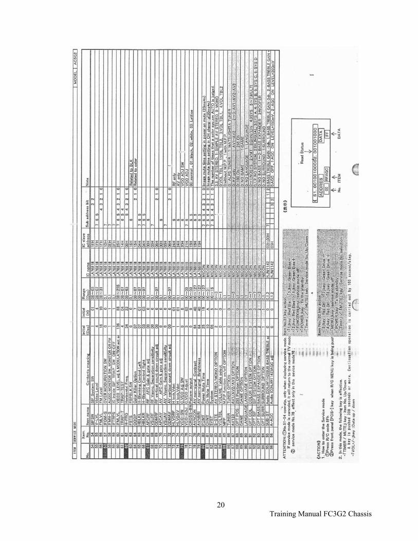
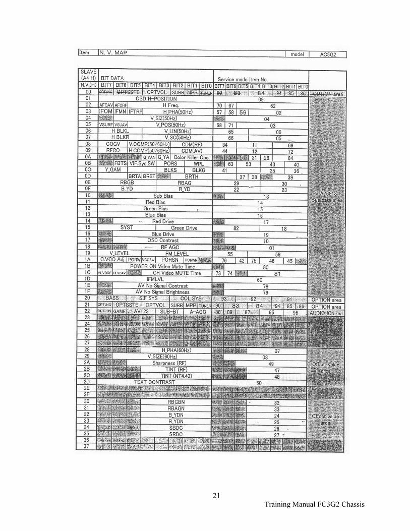
2-7 Service mode
20 Training Manual FC3G2 Chassis
21 Training Manual FC3G2 Chassis

22 Training Manual FC3G2 Chassis
3. IF /Video/Chroma/Deflection The following figure shows a block diagram of the IF/Video/Chroma/Deflection IC LA76818A peripheral circuit.
3-1 IF stage The IF signal output from the tuner is amplified by the pre-amplifier Q111, then sent to the SAW (Surface Acoustic Wave) filter X161. The output signal of the SAW filter X161 is input to pins 5 and 6. The IF signal thus input to the IC is then amplified by the IF amplifier, and is detected by video detector with the VCO (Voltage Controlled Oscillator) circuit consisted of L 171 (38 MHz coil) and it is output as a composite video signal. The composite video signal passes through sound traps then amplified and it is output as a video signal at pin 46. The output of pin 52 is supplied to pin 54, and is detected by FM detector with SPLL (Sound Phase Loop Lock) circuit and it is output as a FM signal at pin 2, and Audio signal at pin 1. 3-2 Video/Chroma stage The video signal output from pin 46 of IC201 is then supplied to pin 44. The external video signal from the A V terminal is supplied to pin 42. The video signal input to pin 44 or 42 is processed in IC201, then seperated into the R (red) at pin 19, G (green) at pin 20, and B (blue) at pin 21. The external RGB signals for the on screen display or teletext display are input to pins 14(R), 15(G), 16(B). In the IC, the external RGB signal are mixed in the selection circuit driven by blanking signal input to pin 17 and finally output to 19, 20, 21. The colour, contrast, brightness, tint and sharpness controls can be controlled by the CPU in 7 bits digital data through the analogue bus lines on pins 11 and 12. 3-3 Deflection stage The Horizontal drive pulse is processed in IC201, and sent from pin27 than drives transistor Q431. The vertical drive pulse is sent from pin 23 of IC201 to pin 1 of IC501, vertical output is from IC LA78041.
SIF APC FILTER
RF AGCOUT
PIF AGC
IF VCC
IF IN
SIF OUT
IF IN
IF GND
APC FILTER
VCO COIL1
VCO FILTER
VIDEO OUTPUT
(2Vpp)FM FILTER
VCO COIL2
EXT.AUDIO IN
AUDIOOUTPUT SIF IN
FM OUTPUT
R291
R181
IC202
R170
C177C133
C276L273C275
R173
C171
R176
R140R245
C185C122
C121
R358
X161
C123
R130R108
C113
C112R114
R116
Q111
R112
R111
C111 R101
R103
D103
R104 C107
TP-A
R109 C106
R107R106
C102
R102
R105
C101
L101
A101
C174
R179
C125
C172
Q173
C132
R132
C135
R244
C124
C138
IC201
R115
R121
R125
X161A
R122D122
R124
Q122
C358
C108C109
R185
L175
X171
JP102
R186
D102
L171
JP111
R178JP174
Q174
R180
R177
Q176
JP176
C176
R188
R174Q171
JP171R175
R172
Q172
JP173
R171 C120
2SJ4.7
X
L78M05CV:BA178M05T:MC78M05CT:
UPC78M05AHF
X
XX
EM47
JEM47
XKK1500GQ
1/16GJ10KC
1/16GZ0C
1/16GJ47KC
X16EM100
KK0.01GQ
1/16GZ0C
SF6376U
1/16GZ0C
1/16GZ0C 18K
KK0.01GQ
KK0.01GQ1/16GJ
330C
1/16GJ56C
2SC2814F4P
1/16GJ5.6KC
1/16GJ1KC
KK0.01GQ
1/16GZ0C
1SJ39K
RD36EB1:MTZJ36A:
DZXLBZA36A
X EM47
J30B0250N:J30B1380N
1/16GJ68KC EM47
100100
X
J
J
16EM470
J
F1BEB0270:F1BEB0300
CD10CGQ
X
X
KK0.01GQ
X
EM0.47
1/16GJ470C
EM0.47
1/16GJ47KC
KK0.01GQ
KK0.022GQ
LA76818AM
56
1/16GJ6.8KC
27K
X
1/16GJ2.2KC1SS356
1/16GJ10KC
AH
EM1
11.IF
9.TB
7.PB
6.M
B
5.DA
TA
4.CL
OCK
3.G
ND
1.AG
C
XX
X
X
X
X
X
X
L14B1830N:L14B1870N
X
X1/16GZ0C
X
X
X
X
1/16GZ0C
X
X
XX
XX
X
X
X
XKK0.022GQ
321
54
53
52
51
50
49
48
47
469
8
7
6
5
4
3
2
1
9V
5V-1
9V
B1130V
5V-1
5V-1

23 Training Manual FC3G2 Chassis
4. Audio Output. The internal audio signal from pin 1 of IC201 is supplied to pin 1 and 30 of IC3701, audio output amp using AN17820B (for stereo model) or AN7523N (for mooral model). The external audio signal is supplied to IC3701(for model with surround option) or IC1201 (for model without surround option). The sound volume control by CPU data. Note : IC3701 (NJW1142MP) is used as audio/tone control IC.
IN1B
IN4B
MONB
TONE-Hb
TONE-Lb
Vcc
OUTb
SR-FIL
VREF
CTH
CTL
LINEbLINEa
GND
SCL
SDA
CVA
CVB
CSR
AGC
OUTa
TONE-La
TONE-Ha
MONA
IN4A
IN3B
IN2B
IN3A
IN2A
IN1A
AUDIO-CONTROL
R OUT
L OUT
R OUT
L OUT
TVL--L
AVL--R
AVL--L
AVR--R
L--R
NC
MONO/ST
NC
GND
VCCL
R
MN/ST
FROM CPU
IIC BUS
D3701
C3702
C3701
C3710 C3720
C3730
C3714
C3731
C3724
C3725
C3735
C3733
R3732
R3731
C3715
C3717
C3727
IC3701
L3701
C3711
C3712
C3713
C3721
C3722
C3723
C3734
C3732
R1204R1201
R1202IC1201
C1201
D1201
C1202
R1205
JP371
JP373
JP372
R3701R3702 R3725 R3726
JP374
JP375
R015
C015
C025
R025
R1203
AA
25KK0.1GQ
16EM470
EM4.7 EM4.7
KK0.022GQ
KK2200GQ
16KZ1GMF
KK2200GQ
16KK0.33BA
EM1
EM1
1/16GJ100C
1/16GJ100C
16KK0.33BA
EM1
EM1
NJW1142MP
J
EM4.7
EM4.7
EM4.7
EM4.7
EM4.7
EM4.7
EM1
16KK0.33BA
XX
X
X
X
X
X
X
X
X
X
XX X X
1/16GZ0C
X
1/16GJ3.3KC
X
X
1/16GJ3.3KC
X
X
30
29
28
27
26
25
24
23
22
21
20
19
18
17
1615
14
13
12
11
10
9
8
7
6
5
4
3
2
18
7
6
54
3
2
1
9V
SCL
SDA9V-1
9V-2
9V-2
LIN
RIN
MNST
R-FI
L-FI
L-RO
R-RO
AOUT
AIN
ATV
R IN
L IN
Vcc
L ou
t +
Gnd
out
L ou
t -
Std
by=
L
L in
Gnd
in
R inVo
l
R o
ut -
Gnd
out
R o
ut +
HEADPHONE
GND AUDIO
R644-H1
JP010
R010
R014
Q011
R022
C022
R013R024
Q021R012
C001
IC001
C021
R032
C011
K001
K002C031
R005
R034
R036
C013
C014
R035
R038
R037
R033
D002
K1001
R006
R007
C034
C035
D003
D004
R008
C060
C059
R052
R051
R023
C012
JP012
JP011
JP011A
C3737
C3738
SP901
SP902
XX
J
X
X
X
X
X
X X
XX
25EM2200LBWA
AN17820B
EM1
1/16GJ27KC
EM1
X
J10EA040N:J10KR040N
EM47
10K
1/16GZ0C
1/16GZ0C
X
X
1.5K
1/16GJ1.5KC
27K
27K
X
J12B06000
1/2DJ150
1/2DJ150
J
J
X
X
X
X
X
X
X
X
X
X
X
X
J
J
A10B26200
A10B26200
12345678910111211V
P.F
9V
9V
FOR WOOFER OUT OPTION
TO CPU
TO CPUMUTE
FROM AUDIO PROCESSOR OUTPUT

24 Training Manual FC3G2 Chassis
5. Vertical The ramp signal, from pin 23 of IC201 drives the vertical drive circuit at pin 1 of IC501. In the first half of scanning period, a deflection current is sent from pin 5 and passed through the following path; Vcc(24V) D512 pin 6 pin 5 DY C515 R518. An electric charge is then stored in C515. In the last half of scanning period, the current path is C515 DY pin 5 pin 4 (GND) R518. In this way, an increasing sawtooth waveform current flows directly to the DY to perform electron beam deflection. During the first half of the blanking period, the vertical ramp signal suddenly turns off. Since there is no longer any current flowing into the DY, the magnetic field in DY collapses causing an induced current to flow as flows; DY pin 5 pin 4 R518 C515 DY. Once the magnetic field in DY has dissipated, the current path becomes; Vcc pin 2 pin 3 C517 pin 6 pin 5 DY C515 R518. And when the prescribed current values is reached, the vertical drive pulse turns on. This completes one cycle. 6. Horizontal Output The horizontal oscillator signal is output from pin 27 of IC201 and used for switching the drive transistor Q431. This switching signal is current amplified by the drive transformer T431 and drives the output transistor Q432. When Q432 turns ON, increasing current flows directly to the DY through D439 C441/C442 L441/R441 L442/R442 DY Q432-C Q432-E. And the deflection occurs during the last half of the scanning period. When Q432 turns off, the magnetic field stored in the DY up to that point causes a resonant current to flow into the capacitors C420/C423 and charges them. The current stored in C420/C423 then flows back to the DY causing an opposite magnetic field to be stored in the DY. This field then collapses increasing a current which switches the dumper diode in Q432 ON. The resonance state is completed, and an increasing current then flows again directly to the DY through the dumper diode. By this means, the deflection in the first half of the scanning period is performed. When Q432 turns ON at the end of the first half of the scanning period, the deflection during the last half is begun, thus completing one cycle. ( see fig. on p. 25 )

25 Training Manual FC3G2 Chassis
Q461-12HEF0068--
PROTECT
VIDEO
ABL
HEATER
AFC
GND
LOW B
+B
PRO
TEC
T
SC
FO
HV
HORIZ.DRIVE
2HEA0236--Q432-1
HEATER
180V
GND
PROTECT
V OUT
H-OUT
65
3
H-DRIVETRANS
1
4
1
PUM
P U
P
VCC
INVE
RT
INPU
T
INPU
T
OU
TPU
TST
G V
CC
OU
TPU
T
GN
D
VERT.DEFLECTION
V-OUTV-OUT
RAMP ALC FILTER
CCD FILTER
CCD VCC
CLOCKOUTPUTH-VCC
VCO IREFH-AFCFILTER
GND
C425
C420
JW1
JWW1
C442-H3 C441-H3
C442-H2
C442-H1
C442
KDY
D439
C461
R474
Q461A
R468
C462
R472
R463
D421L462-H2
VR462D462
R426
R465
C464
R462C540R540Q540
D466
C468
Q461-H1
C467
R467
R461R480
R469
R464
R471
Q462
R473
Q461
L461
C465 C470R466
D461
D469
C463
C466
Q461-H2
L462-H1L462-H3
D465
D642
D438
C424
R48
1
R431
JP408
T471-H8
T471A
Q449
C449 R449
D448
D485R492
R483
R423
R434
C491
L432 C486
R488C434
C432 C437
R479
D468
R424
C471
C469
D467
R47
5
T471-H11
T471-H7
T471-H5
T471
-H2
Q432-H1
Q432-H2
Q432-H3
R435
T471
T431
R355
Q431
C433
R433
Q432
C510
R511
R510
L441-H3
C441-H2
C441-H1
D501
L441-H2
R486
L441
R485
D486
T471
-H1
C527
D512
Q527
R527
R445
C441
R518
R514
R522
C514
R515 R516
C515
D441
R525 C524
C511
D476
T471
-H10
SW501
R501
C517 R519
C520
R512 C518
R422
R484
L441-H1
R432
C431
IC501
D249
R354
C202
R210
JP201
JP202
C201
D352
R241
R352
C230 C210
C231
R286
R212
R211
C232R357
FBP IN
C420-H2
C420-H1
C423-H2
C423-H1
C423-H3
C420-H3
R243
T431-H1
T431-H2 T431-H4
T431-H3
R441
KDY-3
KDY-1
KDY-6
L431
R481A
JP412
JP409
JP410
JP411
JP403
JP404
T471-H6
JP407
T471-H4
JP405
JP483
L442 R442
L442-H1
L442-H2
D210
C423
JP436
C423A
KQ
C487 R487
R502
R359 D357
C424AC425A
C437A
C521
L462
JW36
VR463
JP463
R503 JP503
JP501
JW37
JP435
J
R478
J441
JP477R477
R477A
C355
DY
400NJ0.02EAQ
1500MH6800(AN:XK:VBA)
X 2400030
2400030
2400030
400MJ0.15CQ:250MJ0.15AP:250MJ0.18AU
J10B0730N
ERB44-04
X
1/2DJ1K
X
X
EM0.47
47K
680
MTZJ16A:RD16EB1:
2400010
R3D6472NJ:R3D7472NJ 1.8K
10K
4.7K
EM1
47025PM101KAE
MTZJ20A:RD20EB1
25EM22
2400010
10EM220
1.2M
47047K
82K
12K
1.5K
AE
470
2SB1274(QRA:RRA)
L26B0170N:LM0045(:D)
100GK2.2 KZ
0.01F
1.8K
1SS133
EU1
EM220T
63GK0.39V:HJ0.39G
2400010
2400030X
J
1.5M
ERD07-15L
400NJ0.022EAQ
2SJ4
.7
X
X
2400010
X
X
X X
X
EU1X
X
DJ47K
1/2DJ100
500KK680A
B4Z21B0030N:Z21B0050N:
ZZ0008250EM33CY
1/2FJ135EM47
500KK1000A 250GJ
0.47
1/16GJ2.2KC
AA
1K
100PM2.2(X:LBZAJ)
EM10
P
1/2D
J330
2400010
2400010
2400010
2400030
2400010
2400010
2400010
7SJ6.8VC
L40B16000
AD0002(:C):B4L18B0020N
:L18B0540N
DJ10K
2SC3332(R:S)
500KK3900A
1/2DJ1K
2SD2634YB
16EM22(:LBWAJ)
10K
10K
2400030
X
2400030
J
2400030
X
L71B0160N
X
X
2400030
EM10
EM01Z:ERA15-02
:ED0448
AH
1/16GJ56KC
X
400MJ0.18CQ:250MJ0.18A(P:U)
1SJ1.8
8.2K
470
EM22
39K 1.2K
25EM2200LBWA
ERC05-10B:RM11C
1SJ180100FK0.1(D:BE)
KK0.01GQ
MTZJ11C:RD11EB3
2400010
B4S10B00100:S10B1370N
2SJ1K
35EM220
100
100FK0.1(D:BE)
DJ470 KK3300
DJ47K
X
2400010
1/16GJ1KC
X
LA78041
X
22K
FJ0.015(A:BE:D)
1/16GJ3KC
X
J
PM1
RD5.1EB2
X
DJ10K
X 25EM1000
HJ0.33G
KK0.01GQ
1/16GF4.7KC
150
150
HJ0.33G1.8K
H-OUT
2400030
2400030
2400030
2400030
2400030X
X
2400030
2400030 2400030
2400030
1SJ1K
2400010
2400010
2400010
L7201B:L2G31R0MN
X
X
J
J
X
J
X
2400010
J
2400010
J
J
L26B4560N 2SJ1K
X
X
J
1500MH7800(AN:XK)
J
X
X
X J
X
82K 1SS133
XX
X
35EM2200(:LBWA)
L26A00200:L26B4630N
R3D7102NJ
X
X J
J
X
X
X
X
J X
1SJ560
KK1500
L70B17400
1
1
64
10
11
5 3
2
1
64
7
10
5 3
2
1
7 6 5 4 3 2 1
32
31
30
29
2827
26
25
24
23
1
3
4
1
1
B1130V
5V-1
24V
B1130V
24V
24V
5V-1
9V
HVFOCUSSCREEN
HORIZONTALDEFLECTION
PCCCIRCUIT

26 Training Manual FC3G2 Chassis
7. Power Consumption Saving Circuit. This chassis employs the internal oscillation circuit (SMPS : Switching Mode Power Supply) on the power circuit for saving consumption of power during the stand-by mode. ( see page 26 for circuit diagram of power supply ). The internal oscillation circuit consist of Q663, Q662, D662 and peripheral circuit. Q663 and Q662 drives the photo coupler D610 and oscillation of power circuit according to voltage level on point (A) in figure. During power on mode, the voltage on point (A) is almost 0V and Q663 and Q662 maintain turning off. When the set switches into stand-by mode, the voltage on point (A) increases about 24V. The voltage which is decided with R671 and R673 is applied to Q663-base and drives Q663 and Q662 turning on. When Q662 turns on, the photo-diode in D610 is completely turned on, then Q612 is turned on and Q613 is turned off. By this means, the oscillation of power circuit stops and the voltage of secondary power supply falls down. Also the voltage of point(A) falls down from 24 V gradually. When the voltage on Q663-base is less than voltage of Q663-emitter, Q663 is turn off and then Q662 is off, then D610 and Q612 are turned off. Finally Q613 starts the oscillation and voltages are supplied to the secondary circuit. By this means, the voltage on point (A) rises up and drives Q663 on again. By repeating the above operation, the power consumption in the stand-by mode can be saved.

27 Training Manual FC3G2 Chassis
Fig.
of A
C5G
1 Po
wer
Sup
ply
Circ
uit
21
C605
/.../C
607 D6
05/..
./D60
8
C608
PS60
1
JP60
2
JP60
1
AT3
AT3
R628
R629
C629
D651
C651
R661
R662Q
661
D661
R664
R663
T611
-H8
T611
-H3
T611
B-H1
2
Q65
4
R656
D664
C665
C664
VR65
1
T611
-H5
R669
C639
R668
L612
L611
C616
C618
C617
R626
R625
D611
L613
Q61
3
C615
D612
L614
R631
L615
R633
R632
Q61
1
Q61
2
R623
L616
R622
R620
R621
C613
R619
D614
D615
R627
C614
D617
D616
R641
Q64
1
Q64
2
R642
R644
C644
R643
Q62
5
R611
D619
R616
R614
C611
D610
L651
L654
L653
L652
D652
C652
C643
C654
R654
R652
R658
R657
R659
IC68
1
C681
R655
D659
Q68
1
R682
R681
Q66
2
R666
R667 Q
663
D662
R665
C663
R673
R671
AT3
AT3
AT3
AT3
AT3
AT3
AT3
AT3
AT3
AT3
AT3
AT3
D655
R646
D641
Q61
3-H3
Q61
3-H2
Q61
3-H1
T611
-H6
T611
-H7
R615
D671
R672
R601
VA60
1
L601
C605
D605
D607
C608
C606
C607
AT3
AT3
AT3
AT3
AT3
AT3
D606
D608
C609
AT3
AT3
AT3
AT3
AT3
AUDI
O
L-ST
H-O
N
PRO
TECT
C628
L601
A
D653
D654
A
C619
Q65
1
R651
T611
B-H1
7
C601
C602
C656
C657
C655
C658
Q65
2
D643
C618
A
R602
A
C609
A
Q65
3
Q61
3-H4
Q61
3-H5
Q61
3-H6
C651
-H1
C651
-H2
R613
R624
T611
SW60
1
R653
JP65
2
JP65
3
R660
R645
TP-1
30
D692
C691
C690
D690
R691
Q69
0
D691
R690
R693
R692
R694
JP63
1
JP63
3
Q69
3
R695
R696
R697
D693
C693
C610
D601
D654
-H1
D654
-H2
D654
T611
-H13
T611
-H17
T611
-H12
T611
B-H1
3
T611
-H14
T611
B-H1
4
C653
DHX
AAEV
0070
XJ
2400
030
2400
030
2400
030
1/2C
K5.
6MXG
1/2C
K5.
6MXG
250K
M33
00XN
:25
0KK3
300X
H
RU3A
M
160E
M22
0XJ
DJ10
0K
1/16
GJ
3.9K
C
AH
MTZ
J6.2
C:RD
6.2E
B3:
DZXL
BZA6
.2C1S
J27K
150K
X
2400
030
X
2SD1
913
(QRA
:RRA
)
1SJ2
70
MTZ
J10B
:RD
10EB
2:DZ
XLBZ
A10B
16EM
470
16EM
220:
16EM
220L
BWA
R3D6
222N
J:R3
D722
2NJ
X
2SJ
12
X
2SJ1
2
J
X
X
630G
K0.0
47DC
N
2000
KK22
0CRD
2SJ
68K
2SJ6
8K
EG01
C
ZZ01
22:
ZZ01
22XX
A
2SK
3102
F
2000
KK22
0CRD
ERA8
1-00
4
ZZ01
22(:X
XA)
47K
ZZ01
22(:X
XA)
2SJ0
.33
2SJ
0.27
2SC
2274
(D:E
:F)
2SA9
84(E
:F)
330K
Z21B
0140
B
DJ47
1/2D
J47
0K
1/2D
J47
0KFK
0.1B
E:F
K0.1
D
DJ22
ES1
X22
K
HJ0.
22G
1SS1
33
MTZ
J20B
:RD2
0EB2
10K
AB
AD
47K
22K
25EM
3.3
18K
2SC
2274
(E:F
)
DJ 470
MTZ
J10C
:RD
10EB
3
10K
22K
FJ0.
01BE
:FJ
0.01
D
PC12
3X5Y
FZ:
PC12
3Y52
:TL
P421
F-BL
J
J
J
J
RN1Z
35EM
470T
25EM
1000
T 25EM
3300
15K
33K
X
DJ3.
9K
X
BA17
8M05
T:M
C78M
05CT
:UP
C78M
05AH
F:L7
8M05
CV
10EM
470
DJ10
K
X
AE 1/16
GJ
560K
C
22K
AC
1/16
GJ
22KC
1/16
GJ
10KC
AH
MTZ
J6.
8A:
DZXL
BZA
6.8A
DJ12
K
EM0.
22
1/16
GJ
560K
C
22K
AA
J
J
2400
010
2400
010
2400
010
X
2400
030
220
AA
12K
2400
030
2400
030
2400
030
2400
030
X
ERZV
14D4
71
F35
B057
0N:B
4F35
B004
0N:F
35B1
130N
X
XX1000
KK10
00(C
BB:H
B)
XX
2400
010
2400
010
2400
010
2400
010
2400
010
XX
400E
M22
0XC
X
X
FE30
1-1L
43:
RU4Y
XLF-
L1
2HE
F002
1--
:2HE
F006
5--
F601
4A25
0VTW
:4A2
50VH
OTS
X
AD
1K
X
250G
M0.
1X(B
J:E:
D):
275G
M0.
1(X
B:VB
)
250G
M0.
1X(B
J:D:
E):
275G
M0.
1(V
B:XB
)
2400
010
1000
KK47
0(CR
D:NH
)
1000
KK47
0(C
RD:N
H)
1000
KK68
0(C
RD:N
H)
1000
KK47
0(C
RD:N
H)
2SB1
565E
1SS
133
X
15W
K1.8
(VE:
M)
XX
400E
M22
0XC
2400
010
2400
010
XXX X
X
2400
010
2400
010
X
XX
FJ33
0P
1/2
FJ10
L51B
5900
N
S10B
6230
N
1FJ5
.6
X
1/16
GZ0
C
X
X
X
EU1
35EM
47
EM2.
2CT
1SS3
551/
16G
J47
KC
AH
AA1/
16G
J47
KC
1/16
GJ
10KC
1/16
GJ
20KC
5.6K
J
X
ADDJ
6.8K
1/16
GJ
4.7K
C1/
16G
J47
KC
AA
16EM
47
X
RBV-
608
2400
010
2400
010
YG90
1C2-
LB24
0003
0
2400
030
2400
030
X
X X
2400
010
2400
010
PM1
1 234
12
3
1514 1312 16 17
7654 1 32
12
34
B1 130V
9V
11V
5VRC
24V
11V

28 Training Manual FC3G2 Chassis
Part 2 Block Diagram of ICs 1. LA76818A (IF/VIDEO/CHROMA/DEFLECTION)

29 Training Manual FC3G2 Chassis

30 Training Manual FC3G2 Chassis
2. LA78041N (VERTICAL OUTPUT)
3. AN17820B (AUDIO OUTPUT)

31 Training Manual FC3G2 Chassis
4. LA7642NM (SECAM DECODER)
5. 24LC16B/P (IC MEMORY)
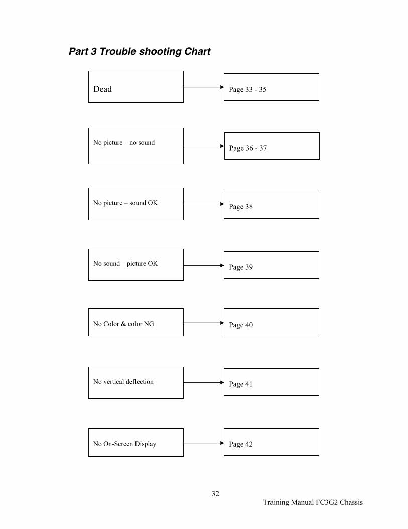
32 Training Manual FC3G2 Chassis
Part 3 Trouble shooting Chart
Dead
No picture – no sound
No picture – sound OK
Page 36 - 37
No sound – picture OK
No Color & color NG
No vertical deflection
No On-Screen Display
Page 33 - 35
Page 42
Page 38
Page 41
Page 40
Page 39

33 Training Manual FC3G2 Chassis
Trouble Shooting Chart Startpoint symptom: Dead
Dead
Is the fuse OK
Check voltage on both ends of C609
Are there any burned part ? Check power primary circuit C601, C602, VA601, PS601, R602, C608, C609, D601/D605~D608, Q611, Q612, Q613, Q625, C613, R624. Secondary circuit, Q661, D661, C651, R661, Q431, Q432.
AC cord, SW601, F601, L601, R602.
Check voltage on pin 1 of IC681
Q611, Q612, Q613, Q625, R620~R626, C651, T611, L614, Q663, Q662, D653, D662, D661
Is the power LED lighting ?
IC681, C681, IC801, IC802, C805
Check voltage (+24V) on Q652-collector
Q652, D652, R653
Check voltage (+130V) on both ends of C651
C651, D651, Q432
Go to next page
YES
NO
0V
0V
+390V~400V
+12.5V
NO
NO
YES
YES
YES
NO

34 Training Manual FC3G2 Chassis
Trouble Shooting Chart Startpoint symptom: Dead Check follows
Disconnect error detector diodes D655, D690, D693, D468
Does horizontal line appear on the screen?
Check voltage on pin 27 of IC801
Check vertical deflection circuit.
R830, IC801, and check error detection lines
Check voltage (+24V) on Q652-collector
Q652, D652, R653
Check voltage (+9V) on Q654-emitor
Q654, R656, R668, R669, D653, C643
NO
YES
0V
+5V
YES
NO
YES
* To avoid the damage to the other circuits, please turn set on for 2-3 seconds for checking.
NO
Go to next page

35 Training Manual FC3G2 Chassis
Troouble Shooting Chart Startpoint symptom: Dead
Check waveform on pin 27 of IC201
Check waveform on Q431-collector
Is the CRT heater coil lighting
C434, T431, R434, Q431, R432, R212
Horizontal Output circuit, Q432, T471, T431, DY, R481
Check voltage on terminal KQ-1
Check voltage (+B) circuit & T471
Check voltage on both ends of C469 (+5V to +10v)
C469, D467, R475
YES
NO
NO
NO
YES
IC201, R211
YES
+180V
0V
0V

36 Training Manual FC3G2 Chassis
Trouble Shooting Chart Startpoint symptom: No picture-no sound
No picture/ No sound
Is CRT heater lighting?
Is video signal observed on pin 44 IC201
Go to chapter “Dead” on page 35
IC201
Is video signal observed on pin 46 of IC201
R140, R141, peripheral circuit for AV switch (IC1401, IC1501)
Check voltage (+36V) on both ends of D103
R103, D103, C107
Go to next page
NO
YES
YES
YES
NO
NO
0V

37 Training Manual FC3G2 Chassis
Trouble Shooting Chart Startpoint symptom: No picture-no sound
Is supply voltage (+5v) observed on terminal pin 6 & 7 of Tuner A101
Check AGC voltage on terminal AGC on the tuner
C106, R109, IC201
IC Memory IC802, R106, R107
Check SDA & SCL SDA ~ 4,1V : SCL ~ 3,9V
Memory Circuit IC801, IC802 AFT Circuit Q111, C111, C113, R111, R112, R114 Video Detector Circuit L171 AFT Circuit from CPU pin 10 to one chip pin 10 : C273, C804 X-SW from CPU pin 33 C823, R815, R125, Q122
Check aerial cable, tuner and IF peripheral circuit X161, Q122, D122, C123, C113, Q111, C111
YES
NO
0 or +12V
NO
IC202, C278, C101
+3V to +6V
OR

38 Training Manual FC3G2 Chassis
Trouble Shooting Chart Startpoint symptom: No picture-sound OK
No picture-sound OK
Is RGB signal observed on IC201 pin 19, 20 & 21
C227, C1502, IC1501, IC201.
9V line to CRT unit
Check 9V line to CRT unit
NO
NO
YES
RGB, VCC. Pin 18 C233, C240, R230, 9V line.
T471, Screen circuit CRT unit, & heater circuit
Is -Y signal observed on pin 42 of IC201
NO
YES

39 Training Manual FC3G2 Chassis
Trouble Shooting Chart Startpoint symptom: No sound-picture OK
No sound-picture OK
Check Vcc 11V
Check input IC001 pin 6, 8
NO
NO
Check D654, C654, IC001
Check Audio out IC201 pin 1
Check speaker, terminal speaker, IC001 output pin 2 & 4 and 10 & 12 (do not reverse polarity)
YES
NO
Check SIF circuit pin 52 IC201 to pin 54 IC201
IC001
Check IC3701 pin 10, 21 (for output) and 1, 30 (for input)
NO
NO
YES

40 Training Manual FC3G2 Chassis
Trouble Shooting Chart Startpoint symptom: No color & color NG
No color & color NG
Check pin 39 IC201, 2.87V
IC201
NO X211, C212
NO
SECAM COLOR
Color Noise Check pin 39: 3.32Vdc 38: 2.85Vdc 37: 1.95Vdc 36: 3.17Vdc 35: 0.93Vpp 34: 0.93Vpp 32: 8.45Vdc 31: 4.58Vdc
IC281, IC201
Check pin 22, IC201, 2V
PAL, NTSC

41 Training Manual FC3G2 Chassis
Trouble Shooting Chart Startpoint symptom: No vertical deflection
No Vertical deflection
Check waveform on pin 5 IC501
R525, C524, R515, R516
NO
+24V
IC201, IC 501
Compressed or expanded vertical screen size
Check voltage on pin 2 of IC501
R514, R515, R516, R518, R522, R525, C514, C515, Service data
D652, R653, Q652
NO
YES

42 Training Manual FC3G2 Chassis
Trouble Shooting Chart Startpoint symptom: No on-screen display
No On Screen Display
Check waveform on pin 18 of IC801
IC801, IC201
NO
YES
Q881, R881, R882, R883, C880, R355
Check waveform on pin 17 of IC801
Q871, R871, R877, R870, C835, R872
NO
YES
Vertical. 5V
Horizontal. 5V

Shor
t ope
n te
st o
f com
pone
nts
Dat
e :
14.
May
. 200
3~
12.
Jun
e. 2
003
Mod
el n
umbe
r:2
1-C
5GJ /
CG
21K
F2G
Ju
dgem
ent:
Fail →
Pas
sSa
mpl
e fo
rm:1
st.E
ngin
eerin
g tri
al
X
: Sh
ort
/ Ope
n th
e co
mpo
nent
s in
pow
er o
ff m
ode
and
test
it w
hen
pow
er tu
rns o
n.
Ass
y, p
wb,
MA
IN C
G21
KF2
G
Y
: Sh
ort
/ Ope
n th
e co
mpo
nent
s in
pow
er o
n m
ode
and
con
firm
it i
s per
form
ance
. C
ircui
tN
o.Lo
catio
nFa
ult m
ode
X:Y
Ras
ter &
Aud
io c
ondi
tion
Circ
uits
& C
ompo
nent
s situ
atio
nsD
amag
e c.
Test
tim
eR
esul
tR
emar
k P
rimar
y01
D60
5Sh
ort
YPo
wer
shut
dow
n.Po
wer
osc
illat
ion
stop
ped.
F601
a m
omen
tPa
ss(D
DER
C05
-10B
-B)
F601
(4A
250V
TW)O
pen.
R60
202
D60
6Sh
ort
YPo
wer
shut
dow
n.Po
wer
osc
illat
ion
stop
ped.
F601
a m
omen
tPa
ss(D
DER
C05
-10B
-B)
F601
(4A
250V
TW)O
pen.
R60
203
D60
7Sh
ort
YPo
wer
shut
dow
n.Po
wer
osc
illat
ion
stop
ped.
F601
a m
omen
tPa
ss(D
DER
C05
-10B
-B)
F601
(4A
250V
TW)O
pen.
R60
204
D60
8Sh
ort
YPo
wer
shut
dow
n.Po
wer
osc
illat
ion
stop
ped.
F601
a m
omen
tPa
ss(D
DER
C05
-10B
-B)
F601
(4A
250V
TW)O
pen.
R60
205
R62
1O
pen
YN
o pr
oble
m.
No
circ
uit a
nd c
ompo
nent
dam
aged
.**
180s
Pass
(RD
A56
03JP
CA
NB
)X
No
prob
lem
.N
o ci
rcui
t and
com
pone
nt d
amag
ed.
****
Pass
06R
626
Ope
nX
.YN
o pr
oble
m.
No
circ
uit a
nd c
ompo
nent
dam
aged
.**
180s
Pass
(RS2
6802
JGD
AN
N)
07C
613
Shor
tY
Pow
er sh
ut d
own.
No
circ
uit a
nd c
ompo
nent
dam
aged
.**
a m
omen
tPa
ss(C
F1H
104K
AD
AJC
)X
No
pow
er o
pera
te.
No
pow
er o
scill
atio
n st
arte
d.**
**Pa
ssO
pen
YN
o pr
oble
m.
No
circ
uit a
nd c
ompo
nent
dam
aged
.**
180s
Pass
XN
o pr
oble
m.
No
circ
uit a
nd c
ompo
nent
dam
aged
.**
180s
Pass
08R
622
Ope
nY
Pow
er sh
ut d
own.
No
circ
uit a
nd c
ompo
nent
dam
aged
.**
a m
omen
tPa
ss(R
DB
47R
0JPB
AN
B)
XN
o po
wer
ope
rate
.N
o po
wer
osc
illat
ion
star
ted.
****
Pass
09R
623
Ope
nY
No
prob
lem
.N
o ci
rcui
t and
com
pone
nt d
amag
ed.
**a
mom
ent
Pass
(RD
D47
03JP
AA
NB
)X
No
pow
er o
pera
te.
No
pow
er o
scill
atio
n st
arte
d.**
**Pa
ssN
oisy
soun
d of
an
Inte
rmitt
ent o
scill
atio
n 10
Q61
1B
-C S
hort
YP
ower
shu
t dow
n.P
ower
osc
illat
ion
stop
ed.
a m
omen
tP
ass
T2S
C22
74-E
--C
Q62
5 (T
2SC
2274
-E--
C) A
ll S
hort
Q62
5Q
613
(T2S
K31
02-F
--N
) All
Sho
rtQ
613
Q61
2 (T
2SA
984-
E--
-C) A
ll S
hort
Q61
2Q
641
(TX
XA
AQ
6562
G-C
) All
Sho
rtQ
641
R63
2 (R
S2R
220J
GD
AN
N) O
pen
R63
2R
624
(RFX
AA
A10
R0J
FN) O
pen
R62
4R
613
(RFX
AA
A12
01JF
N) O
pen
R61
3
43

Q61
1 (T
2SC
2274
-D--
C) A
ll S
hort
Q61
1
Prim
ary
10Q
611
B-E
Sho
rtY
Pow
er s
hut d
own.
Pow
er o
scill
atio
n st
oped
.a
mom
ent
Pas
sT2
SC
2274
-E--
CQ
625
(T2S
C22
74-E
--C
) All
Sho
rtQ
625
Q61
3 (T
2SK
3102
-F--
N) A
ll S
hort
Q61
3Q
612
(T2S
A98
4-E
---C
) All
Sho
rtQ
612
Q64
1 (T
XX
AA
Q65
62G
-C) A
ll S
hort
Q64
1R
632
(RS
2R22
0JG
DA
NN
) Ope
nR
632
R62
4 (R
FXA
AA
10R
0JFN
) Ope
nR
624
R61
3 (R
FXA
AA
1201
JFN
) Ope
nR
613
Q61
1 (T
2SC
2274
-D--
C) A
ll S
hort
Q61
1
C-E
Sho
rt.Y
Pow
er s
hut d
own.
Pow
er o
sclla
tion
stop
ped.
a m
omen
tP
ass
Q62
5 (T
2SC
2274
-E--
C) A
ll S
hort
Q62
5Q
613
(T2S
K31
02-F
--N
) All
Sho
rtQ
613
Q61
2 (T
2SA
984-
E--
-C) A
ll S
hort
Q61
2Q
641
(TX
XA
AQ
6562
G-C
) All
Sho
rtQ
641
R63
2 (R
S2R
220J
GD
AN
N) O
pen
R63
2R
624
(RFX
AA
A10
R0J
FN) O
pen
R62
4R
613
(RFX
AA
A12
01JF
N) O
pen
R61
3Q
611
(T2S
C22
74-D
--C
) All
Sho
rtQ
611
B O
pen
YP
ower
shu
t dow
n.P
ower
osc
illat
ion
stop
ped.
a m
omen
tP
ass
Q62
5 (T
2SC
2274
-E--
C) A
ll S
hort
Q62
5Q
613
(T2S
K31
02-F
--N
) All
Sho
rtQ
613
Q61
2 (T
2SA
984-
E--
-C) A
ll S
hort
Q61
2Q
641
(TX
XA
AQ
6562
G-C
) All
Sho
rtQ
641
Q61
1 (T
2SC
2274
-D--
C) A
ll S
hort
Q61
1R
632
(RS
2R22
0JG
DA
NN
) Ope
nR
632
R62
4 (R
FXA
AA
10R
0JFN
) Ope
nR
624
R61
3 (R
FXA
AA
1201
JFN
) Ope
nR
613
C O
pen
YP
ower
shu
t dow
n.P
ower
osc
llatio
n st
oppe
d.a
mom
ent
Pas
sQ
625
(T2S
C22
74-E
--C
) All
Sho
rtQ
625
Q61
3 (T
2SK
3102
-F--
N) A
ll S
hort
Q61
3Q
612
(T2S
A98
4-E
---C
) All
Sho
rtQ
612
Q64
1 (T
XX
AA
Q65
62G
-C) A
ll S
hort
Q64
1R
632
(RS
2R22
0JG
DA
NN
) Ope
nR
632
R62
4 (R
FXA
AA
10R
0JFN
) Ope
nR
624
R61
3 (R
FXA
AA
1201
JFN
) Ope
nR
613
Q61
1 (T
2SC
2274
-D--
C) A
ll S
hort
Q61
111
Q61
1E
Ope
n Y
Pow
er s
hut d
own.
Pow
er o
scill
atio
n st
oppe
d.a
mom
ent
Pas
s
44

T2S
C22
74-E
--C
Q62
5 (T
2SC
2274
-E--
C) A
ll S
hort
Q62
5Q
613
(T2S
K31
02-F
--N
) All
Sho
rtQ
613
Q61
2 (T
2SA
984-
E--
-C) A
ll S
hort
Q61
2Q
641
(TX
XA
AQ
6562
G-C
) All
Sho
rtQ
641
Q61
1 (T
2SC
2274
-D--
C) A
ll S
hort
Q61
1R
632
(RS
2R22
0JG
DA
NN
) Ope
nR
632
R62
4 (R
FXA
AA
10R
0JFN
) Ope
nR
624
R61
3 (R
FXA
AA
1201
JFN
) Ope
nR
613
Prim
ary
12Q
612
B-C
Sho
rtY
Pow
er s
hut d
own.
Pow
er o
scill
atio
n st
oppe
d.**
a m
omen
tP
ass
T2S
A98
4-E
---C
XN
o po
wer
ope
rate
.N
o po
wer
osc
illat
ion
star
ted.
****
Pas
sB
-E S
hort
YP
ower
shu
t dow
n.P
ower
osc
illat
ion
stop
ped.
a m
omen
tP
ass
Q62
5 (T
2SC
2274
-E--
C) A
ll S
hort
Q62
5Q
613
(T2S
K31
02-F
--N
) All
Sho
rtQ
613
Q61
2 (T
2SA
984-
E--
-C) A
ll S
hort
Q61
2Q
641
(TX
XA
AQ
6562
G-C
) All
Sho
rtQ
641
Q61
1 (T
2SC
2274
-D--
C) A
ll S
hort
Q61
1R
632
(RS
2R22
0JG
DA
NN
) Ope
nR
632
R62
4 (R
FXA
AA
10R
0JFN
) Ope
nR
624
R61
3 (R
FXA
AA
1201
JFN
) Ope
nR
613
C-E
Sho
rt.Y
Pow
er s
hut d
own.
Pow
er o
scill
atio
n st
oppe
d.**
a m
omen
tP
ass
XN
o po
wer
ope
rate
.N
o po
wer
osc
illat
ion
star
ted.
****
Pas
sB
Ope
nY
Pow
er s
hut d
own.
Pow
er o
scill
atio
n st
oppe
d.a
mom
ent
Pas
sQ
625
(T2S
C22
74-E
--C
) All
Sho
rtQ
625
Q61
3 (T
2SK
3102
-F--
N) A
ll S
hort
Q61
3Q
612
(T2S
A98
4-E
---C
) All
Sho
rtQ
612
Q64
1 (T
XX
AA
Q65
62G
-C) A
ll S
hort
Q64
1Q
611
(T2S
C22
74-D
--C
) All
Sho
rtQ
611
R63
2 (R
S2R
220J
GD
AN
N) O
pen
R63
2R
624
(RFX
AA
A10
R0J
FN) O
pen
R62
4R
613
(RFX
AA
A12
01JF
N) O
pen
R61
3E
Ope
n Y
Pow
er s
hut d
own.
Pow
er o
scill
atio
n st
oppe
d.a
mom
ent
Pas
sQ
625
(T2S
C22
74-E
--C
) All
Sho
rtQ
625
Q61
3 (T
2SK
3102
-F--
N) A
ll S
hort
Q61
3Q
612
(T2S
A98
4-E
---C
) All
Sho
rtQ
612
Q64
1 (T
XX
AA
Q65
62G
-C) A
ll S
hort
Q64
1Q
611
(T2S
C22
74-D
--C
) All
Sho
rtQ
611
R63
2 (R
S2R
220J
GD
AN
N) O
pen
R63
2R
624
(RFX
AA
A10
R0J
FN) O
pen
R62
4R
613
(RFX
AA
A12
01JF
N) O
pen
R61
313
R62
4O
pen
YP
ower
shu
t dow
n.P
ower
osc
illat
ion
stop
ped.
**a
mom
ent
Pas
s
45

(RFX
AA
A10
R0J
FN)
XN
o po
wer
ope
rate
.N
o po
wer
osc
illat
ion
star
ted.
****
Pas
s14
D61
4Sh
ort
X.Y
Pow
er s
hut d
own.
P
ower
osc
illat
ion
stop
ped.
**a
mom
ent
Pas
s(D
DE
S1-
----
--B
)O
pen
YP
ower
shu
t dow
nP
ower
osc
illat
ion
stop
ped.
a m
omen
tP
ass
Q62
5 (T
2SC
2274
-E--
C) A
ll S
hort
Q62
5Q
613
(T2S
K31
02-F
--N
) All
Sho
rtQ
613
Q61
2 (T
2SA
984-
E--
-C) A
ll S
hort
Q61
2Q
641
(TX
XA
AQ
6562
G-C
) All
Sho
rtQ
641
Q61
1 (T
2SC
2274
-D--
C) A
ll S
hort
Q61
1R
632
(RS
2R22
0JG
DA
NN
) Ope
nR
632
R62
4 (R
FXA
AA
10R
0JFN
) Ope
nR
624
R61
3 (R
FXA
AA
1201
JFN
) Ope
nR
613
XN
o po
wer
ope
rate
No
pow
er o
scill
atio
n st
arte
d.a
mom
ent
Pas
sQ
625
(T2S
C22
74-E
--C
) All
Sho
rtQ
625
Q61
3 (T
2SK
3102
-F--
N) A
ll S
hort
Q61
3Q
612
(T2S
A98
4-E
---C
) All
Sho
rtQ
612
Q64
1 (T
XX
AA
Q65
62G
-C) A
ll S
hort
Q64
1Q
611
(T2S
C22
74-D
--C
) All
Sho
rtQ
611
R63
2 (R
S2R
220J
GD
AN
N) O
pen
R63
2R
624
(RFX
AA
A10
R0J
FN) O
pen
R62
4R
613
(RFX
AA
A12
01JF
N) O
pen
R61
3P
rimar
y15
D61
9Sh
ort
X.Y
No
prob
lem
.N
o ci
rcui
t and
com
pone
nt d
amag
ed.
**18
0sP
ass
DZM
TZJ8
.2C
--B
Ope
nX
-YN
o p
robl
em
.N
o c
ircuit a
nd
com
ponent
dam
aged.
**
180s
Pass
16R
631
Ope
nX
.YN
o pr
oble
m.
No
circ
uit a
nd c
ompo
nent
dam
aged
.**
180s
Pass
(RD
D47
02JP
AA
NB
)17
Q61
3G
-D S
hort
YP
ower
shu
t dow
n.P
ower
osc
illat
ion
stop
ped.
a m
omen
tP
ass
T2S
K31
02-F
--N
Q62
5 (T
2SC
2274
-E--
C) A
ll S
hort
Q62
5Q
613
(T2S
K31
02-F
--N
) All
Sho
rtQ
613
Q61
2 (T
2SA
984-
E--
-C) A
ll S
hort
Q61
2Q
641
(TX
XA
AQ
6562
G-C
) All
Sho
rtQ
641
R63
2 (R
S2R
220J
GD
AN
N) O
pen
R63
2R
624
(RFX
AA
A10
R0J
FN) O
pen
R62
4R
613
(RFX
AA
A12
01JF
N) O
pen
R61
3G
-S S
hort
YP
ower
shu
t dow
n.P
ower
osc
illat
ion
stop
ped.
**a
mom
ent
Pas
sX
No
pow
er o
pera
te.
No
pow
er o
scill
atio
n st
arte
d.**
**P
ass
18Q
613
D-S
Sho
rtY
Pow
er s
hut d
own.
Pow
er o
scill
atio
n st
oppe
d.a
mom
ent
Pas
sT2
SK
3102
-F--
NQ
625
(T2S
C22
74-E
--C
) All
Sho
rtQ
625
Q61
3 (T
2SK
3102
-F--
N) A
ll S
hort
Q61
3Q
612
(T2S
A98
4-E
---C
) All
Sho
rtQ
612
R63
2 (R
S2R
220J
GD
AN
N) O
pen
R63
2
46

R62
4 (R
FXA
AA
10R
0JFN
) Ope
nR
624
R61
3 (R
FXA
AA
1201
JFN
) Ope
nR
613
G O
pen
YP
ower
shu
t dow
n.P
ower
osc
illat
ion
stop
ped.
**2s
Pas
sR
632
(RS
2R22
0JG
DA
NN
) Ope
nR
632
Q61
3 (T
2SK
3102
-F--
N) A
ll S
hort
Q61
3R
613
(RFX
AA
A12
01JF
N) O
pen
R61
3
Prim
ary
18Q
613
S O
pen
YP
ower
shu
t dow
n.P
ower
osc
illat
ion
stop
ped.
a m
omen
tP
ass
T2S
K31
02-F
--N
Q61
3 (T
2SK
3102
-F--
N) A
ll S
hort
Q61
3
19C
615
Shor
tY
Pow
er S
hot D
own
Pow
er o
scill
atio
n st
oppe
d.a
mom
ent
Pas
s(C
K3D
471K
AN
HN
C)
Q62
5 (T
2SC
2274
-E--
C) A
ll S
hort
Q62
5Q
613
(T2S
K31
02-F
--N
) All
Sho
rtQ
613
Q61
2 (T
2SA
984-
E--
-C) A
ll S
hort
Q61
2Q
641
(TX
XA
AQ
6562
G-C
) All
Sho
rtQ
641
R63
2 (R
S2R
220J
GD
AN
N) O
pen
R63
2R
624
(RFX
AA
A10
R0J
FN) O
pen
R62
4R
613
(RFX
AA
A12
01JF
N) O
pen
R61
3Q
611
(T2S
C22
74-D
--C
) All
Sho
rtQ
611
Ope
nX
.YN
o pr
oble
m.
No
circ
uit a
nd c
ompo
nent
dam
aged
.**
180s
Pas
s20
D61
2Sh
ort
X.Y
No
prob
lem
.N
o ci
rcui
t and
com
pone
nt d
amag
ed.
**18
0sP
ass
(1S
S13
3)O
pen
X.Y
No
prob
lem
.N
o ci
rcui
t and
com
pone
nt d
amag
ed.
**18
0sP
ass
21L6
14O
pen
YP
ower
shu
t dow
n.P
ower
osc
illat
ion
stop
ped.
**a
mom
ent
Pas
s(Z
Z012
2)X
No
pow
er o
pera
te.
No
pow
er o
scill
atio
n st
arte
d.**
**P
ass
22R
627
Ope
nX
.YN
o pr
oble
m.
No
circ
uit a
nd c
ompo
nent
dam
aged
.**
**P
ass
(RD
D22
02JP
AA
NB
)S
hort
YP
ower
shu
t dow
nP
ower
osc
illat
ion
stop
ped.
a m
omen
tP
ass
Q62
5 (T
2SC
2274
-E--
C) A
ll S
hort
Q62
5Q
613
(T2S
K31
02-F
--N
) All
Sho
rtQ
613
Q61
2 (T
2SA
984-
E--
-C) A
ll S
hort
Q61
2Q
641
(TX
XA
AQ
6562
G-C
) All
Sho
rtQ
641
R63
2 (R
S2R
220J
GD
AN
N) O
pen
R63
2R
624
(RFX
AA
A10
R0J
FN) O
pen
R62
4R
613
(RFX
AA
A12
01JF
N) O
pen
R61
3Q
611
(T2S
C22
74-D
--C
) All
Sho
rtQ
611
R60
2 (R
WX
AA
Z1R
8KK
AN
)Ope
nR
602
XN
o po
wer
ope
rate
No
pow
er o
scill
atio
n st
arte
d.a
mom
ent
Pas
sQ
625
(T2S
C22
74-E
--C
) All
Sho
rtQ
625
Q61
3 (T
2SK
3102
-F--
N) A
ll S
hort
Q61
3
47

Q61
2 (T
2SA
984-
E--
-C) A
ll S
hort
Q61
2Q
641
(TX
XA
AQ
6562
G-C
) All
Sho
rtQ
641
R63
2 (R
S2R
220J
GD
AN
N) O
pen
R63
2R
624
(RFX
AA
A10
R0J
FN) O
pen
R62
4R
613
(RFX
AA
A12
01JF
N) O
pen
R61
3Q
611
(T2S
C22
74-D
--C
) All
Sho
rtQ
611
R60
2 (R
WX
AA
Z1R
8KK
AN
)Ope
nR
602
Prim
ary
23C
614
Shor
tY
No
prob
lem
.N
o ci
rcui
t and
com
pone
nt d
amag
ed.
**18
0sP
ass
(CH
1H22
4JA
GA
JC)
XN
o po
wer
ope
rate
.N
o po
wer
osc
illat
ion
star
ted
**a
mom
ent
Pas
sO
pen
X.Y
No
prob
lem
.N
o ci
rcui
t and
com
pone
nt d
amag
ed.
**18
0sP
ass
24D
617
Shor
tX
.YN
o pr
oble
m.
No
circ
uit a
nd c
ompo
nent
dam
aged
.**
180s
Pas
s(1
SS
133)
Ope
nX
.YN
o pr
oble
m.
No
circ
uit a
nd c
ompo
nent
dam
aged
.**
180s
Pas
s25
R64
1O
pen
X.Y
No
prob
lem
.N
o ci
rcui
t and
com
pone
nt d
amag
ed.
**18
0sPa
ss(R
DD
1002
JPA
AN
B)
26Q
642
B-C
Sho
rtY
No
prob
lem
.N
o ci
rcui
t and
com
pone
nt d
amag
ed.
**18
0sP
ass
T2S
C18
15-G
R-C
XN
o pr
oble
m.
No
circ
uit a
nd c
ompo
nent
dam
aged
.**
180s
Pas
sB
-E S
hort
YP
ictu
re is
bro
ken
No
circ
uit a
nd c
ompo
nent
dam
aged
.**
180s
Pas
sX
Pic
ture
is b
roke
nN
o ci
rcui
t and
com
pone
nt d
amag
ed.
**18
0sP
ass
C-E
Sho
rtX
.YN
o pr
oble
m.
No
circ
uit a
nd c
ompo
nent
dam
aged
.**
180s
Pas
s27
Q64
1B
-C S
hort
YN
o pr
oble
m.
No
circ
uit a
nd c
ompo
nent
dam
aged
.**
180s
Pas
s(T
XX
AA
Q65
62G
-C)
XN
o pr
oble
m.
No
circ
uit a
nd c
ompo
nent
dam
aged
.**
180s
Pass
B-E
Sho
rtY
No
prob
lem
.N
o ci
rcui
t and
com
pone
nt d
amag
ed.
**180s
Pas
sX
No
prob
lem
.N
o ci
rcui
t and
com
pone
nt d
amag
ed.
**18
0sPa
ssC
-E S
hort
YH
oris
onta
l pic
ture
mor
e w
ide
No
circ
uit a
nd c
ompo
nent
dam
aged
.**
180s
Pas
sX
Hor
ison
tal p
ictu
re m
ore
wid
eN
o po
wer
osc
illat
ion
star
ted.
**18
0sP
ass
28Q
625
B-C
Sho
rtY
Pow
er s
hut d
own.
Pow
er o
scill
atio
n st
oppe
d.**
a m
omen
tP
ass
(T2S
C22
74-E
--C
)X
No
pow
er o
pera
te.
No
pow
er o
scill
atio
n st
arte
d.**
**P
ass
B-E
Sho
rtY
Pow
er s
hut d
own.
Pow
er o
scill
atio
n st
oppe
d.a
mom
ent
Pas
sQ
625
(T2S
C22
74-E
--C
) All
Sho
rtQ
625
Q61
3 (T
2SK
3102
-F--
N) A
ll S
hort
Q61
3Q
612
(T2S
A98
4-E
---C
) All
Sho
rtQ
612
Q64
1 (T
XX
AA
Q65
62G
-C) A
ll S
hort
Q64
1R
632
(RS
2R22
0JG
DA
NN
) Ope
nR
632
R62
4 (R
FXA
AA
10R
0JFN
) Ope
nR
624
R61
3 (R
FXA
AA
1201
JFN
) Ope
nR
613
Q61
1 (T
2SC
2274
-D--
C) A
ll S
hort
Q61
1C
-E S
hort
YP
ower
shu
t dow
n.P
ower
osc
illat
ion
stop
ped.
**a
mom
ent
Pas
sX
No
pow
er o
pera
te.
No
pow
er o
scill
atio
n st
arte
d.**
**P
ass
B O
pen
YP
ower
shu
t dow
n.P
ower
osc
illat
ion
stop
ped.
a m
omen
tP
ass
48

Q62
5 (T
2SC
2274
-E--
C) A
ll S
hort
Q62
5Q
613
(T2S
K31
02-F
--N
) All
Sho
rtQ
613
Q61
2 (T
2SA
984-
E--
-C) A
ll S
hort
Q61
2Q
641
(TX
XA
AQ
6562
G-C
) All
Sho
rtQ
641
R63
2 (R
S2R
220J
GD
AN
N) O
pen
R63
2R
624
(RFX
AA
A10
R0J
FN) O
pen
R62
4R
613
(RFX
AA
A12
01JF
N) O
pen
R61
3Q
611
(T2S
C22
74-D
--C
) All
Sho
rtQ
611
29Q
625
C O
pen
YP
ower
shu
t dow
n.P
ower
osc
illat
ion
stop
ped.
a m
omen
tP
ass
(T2S
C22
74-E
--C
)Q
625
(T2S
C22
74-E
--C
) All
Sho
rtQ
625
Q61
3 (T
2SK
3102
-F--
N) A
ll S
hort
Q61
3
Q61
2 (T
2SA
984-
E--
-C) A
ll S
hort
Q61
2Q
641
(TX
XA
AQ
6562
G-C
) All
Sho
rtQ
641
R63
2 (R
S2R
220J
GD
AN
N) O
pen
R63
2R
624
(RFX
AA
A10
R0J
FN) O
pen
R62
4R
613
(RFX
AA
A12
01JF
N) O
pen
R61
3Q
611
(T2S
C22
74-D
--C
) All
Sho
rtQ
611
E O
pen
YP
ower
shu
t dow
n.P
ower
osc
illat
ion
stop
ped.
a m
omen
tP
ass
Q62
5 (T
2SC
2274
-E--
C) A
ll S
hort
Q62
5Q
613
(T2S
K31
02-F
--N
) All
Sho
rtQ
613
Q61
2 (T
2SA
984-
E--
-C) A
ll S
hort
Q61
2Q
641
(TX
XA
AQ
6562
G-C
) All
Sho
rtQ
641
R63
2 (R
S2R
220J
GD
AN
N) O
pen
R63
2R
624
(RFX
AA
A10
R0J
FN) O
pen
R62
4R
613
(RFX
AA
A12
01JF
N) O
pen
R61
3Q
611
(T2S
C22
74-D
--C
) All
Sho
rtQ
611
Prim
ary
30R
632
Ope
nX
.YN
o pr
oble
m.
No
circ
uit a
nd c
ompo
nent
dam
aged
.**
180s
Pas
s(R
S2R
220J
GD
AN
N)
31C
611
Shor
tY
Pow
er s
hut d
own.
Pow
er o
scill
atio
n st
oppe
d.a
mom
ent
Pas
s(C
F1H
103J
AD
AJC
)Q
625
(T2S
C22
74-E
--C
) All
Sho
rtQ
625
Q61
3 (T
2SK
3102
-F--
N) A
ll S
hort
Q61
3Q
612
(T2S
A98
4-E
---C
) All
Sho
rtQ
612
Q64
1 (T
XX
AA
Q65
62G
-C) A
ll S
hort
Q64
1R
632
(RS
2R22
0JG
DA
NN
) Ope
nR
632
R62
4 (R
FXA
AA
10R
0JFN
) Ope
nR
624
R61
3 (R
FXA
AA
1201
JFN
) Ope
nR
613
Q61
1 (T
2SC
2274
-D--
C) A
ll S
hort
Q61
1O
pen
YP
ictu
re is
bro
ken
for a
whi
le
o
ffP
ower
osc
illat
ion
stop
ped.
**2s
Pas
sQ
625
(T2S
C22
74-E
--C
) All
Sho
rtQ
625
Q61
3 (T
2SK
3102
-F--
N) A
ll S
hort
Q61
3
49

Q61
2 (T
2SA
984-
E--
-C) A
ll S
hort
Q61
2Q
641
(TX
XA
AQ
6562
G-C
) All
Sho
rtQ
641
R63
2 (R
S2R
220J
GD
AN
N) O
pen
R63
2R
624
(RFX
AA
A10
R0J
FN) O
pen
R62
4R
613
(RFX
AA
A12
01JF
N) O
pen
R61
3Q
611
(T2S
C22
74-D
--C
) All
Sho
rtQ
611
32R
643
Ope
nX
.YP
ictu
re is
bro
ken
No
circ
uit a
nd c
ompo
nent
dam
aged
**18
0sP
ass
(RD
D18
02JP
AA
NB
)33
R64
4O
pen
YN
o pr
oble
m.
No
circ
uit a
nd c
ompo
nent
dam
aged
.**
180s
Pas
s(R
DD
2202
JPA
AN
B)
34R
642
Ope
nX
.YN
o pr
oble
m.
No
circ
uit a
nd c
ompo
nent
dam
aged
.**
180s
Pas
s(R
DD
4702
JPA
AN
B)
Prim
ary
35R
615
Ope
nY
Pow
er s
hut d
own.
Pow
er o
scill
atio
n st
oppe
d.a
mom
ent
Pas
s(R
DD
1001
JPA
AN
B)
Q62
5 (T
2SC
2274
-E--
C) A
ll S
hort
Q62
5Q
613
(T2S
K31
02-F
--N
) All
Sho
rtQ
613
Q61
2 (T
2SA
984-
E--
-C) A
ll S
hort
Q61
2Q
641
(TX
XA
AQ
6562
G-C
) All
Sho
rtQ
641
R63
2 (R
S2R
220J
GD
AN
N) O
pen
R63
2R
624
(RFX
AA
A10
R0J
FN) O
pen
R62
4R
613
(RFX
AA
A12
01JF
N) O
pen
R61
3Q
611
(T2S
C22
74-D
--C
) All
Sho
rtQ
611
R60
2 (R
WX
AA
Z1R
8KK
AN
)Ope
nR
602
XN
o po
wer
ope
rate
No
pow
er o
scila
tion
oper
ate
a m
omen
t18
0sQ
625
(T2S
C22
74-E
--C
) All
Sho
rtQ
625
Q61
3 (T
2SK
3102
-F--
N) A
ll S
hort
Q61
3Q
612
(T2S
A98
4-E
---C
) All
Sho
rtQ
612
Q64
1 (T
XX
AA
Q65
62G
-C) A
ll S
hort
Q64
1R
632
(RS
2R22
0JG
DA
NN
) Ope
nR
632
R62
4 (R
FXA
AA
10R
0JFN
) Ope
nR
624
R61
3 (R
FXA
AA
1201
JFN
) Ope
nR
613
Q61
1 (T
2SC
2274
-D--
C) A
ll S
hort
Q61
1R
620
(RD
A56
03JP
CA
NB
)R
620
R62
7 (R
DD
2202
JPA
AN
B) O
pen
R62
7D
654
(DD
YG
901C
2-LB
N)
R61
9
36R
613
Ope
nY
No
prob
lem
.N
o ci
rcui
t and
com
pone
nt d
amag
ed.
**18
0sP
ass
(RFX
AA
A12
01JF
N)
XS
tand
by
mod
eN
o ci
rcui
t and
com
pone
nt d
amag
ed.
**18
0sP
ass
130
V37
C65
1S
hort
YP
ower
Shu
t Dow
nP
ower
Osc
ilatio
n S
tope
d(M
ain
B)
CE
XA
A2C
221A
JNQ
625
(T2S
C22
74-E
--C
) All
Sho
rtQ
625
a m
omen
tP
ass
Q61
3 (T
2SK
3102
-F--
N) A
ll S
hort
Q61
3
50

Q61
2 (T
2SA
984-
E--
-C) A
ll S
hort
Q61
2R
632
(RS
2R22
0JG
DA
NN
) Ope
nR
632
R62
4 (R
FXA
AA
10R
0JFN
) Ope
nR
624
R61
3 (R
FXA
AA
1201
JFN
) Ope
nR
613
38D
651
Ope
nY
Pow
er S
hut D
own
Pow
er O
scila
tion
Sto
ped
DD
RU
3AM
----
-BIC
501
(QLA
7804
0N--
-N)
IC50
1a
mom
ent
Pas
sIC
001
(QA
N17
820B
---N
)IC
001
Sho
rtY
Pow
er S
hut D
own
Pow
er O
scila
tion
Sto
ped
Q62
5 (T
2SC
2274
-E--
C) A
ll S
hort
Q62
518
0sP
ass
Q61
3 (T
2SK
3102
-F--
N) A
ll S
hort
Q61
3Q
612
(T2S
A98
4-E
---C
) All
Sho
rtQ
612
R63
2 (R
S2R
220J
GD
AN
N) O
pen
R63
2R
624
(RFX
AA
A10
R0J
FN) O
pen
R62
4R
613
(RFX
AA
A12
01JF
N) O
pen
R61
313
0 V
39R
663
Ope
nX
.YN
o pr
oble
m.
No
circ
uit a
nd c
ompo
nent
dam
aged
.**
180s
Pas
s(M
ain
B)
(RD
D15
03JP
AA
NB
)40
R10
3O
pen
X.Y
Noi
se c
omes
out
in s
cree
n.N
o ci
rcui
t and
com
pone
nt d
amag
ed.
**18
0sP
ass
(RS
1390
2JG
CA
NN
)41
D10
3S
hort
X.Y
No
tunn
er o
scill
ated
.N
o ci
rcui
t and
com
pone
nt d
amag
ed.
**18
0sP
ass
(DZM
TZJ3
6A--
-B)
Ope
nX
.YN
o pr
oble
m.
No
circ
uit a
nd c
ompo
nent
dam
aged
.**
180s
Pas
s42
C10
7S
hort
X.Y
Pic
ture
is b
roke
nN
o ci
rcui
t and
com
pone
nt d
amag
ed.
**18
0sP
ass
(CE
XLB
1H47
0WA
J)O
pen
X.Y
No
prob
lem
.N
o ci
rcui
t and
com
pone
nt d
amag
ed.
**18
0sP
ass
Ver
tical
43D
512
Sho
rtY
Num
ber o
f cha
nel r
un u
pN
o ci
rcui
t and
com
pone
nt d
amag
ed.
**18
0sP
ass
def
lect
ion
(DD
ER
A15
-02-
-B)
XN
o pr
oble
m.
No
circ
uit a
nd c
ompo
nent
dam
aged
.**
180s
Pas
sO
pen
X・Y
No
verti
cal d
efle
ctio
n op
erat
e. (O
ne li
ne)
No
circ
uit a
nd c
ompo
nent
dam
aged
.**
180s
Pas
s V
ertic
al44
R51
0O
pen
X.Y
No
verti
cal d
efle
ctio
n op
erat
e.(O
ne li
ne)
No
circ
uit a
nd c
ompo
nent
dam
aged
.**
180s
Pas
sde
flect
ion
(R
DD
1002
JPA
AN
B)
45R
511
Ope
nX
.YN
o ve
rtica
l def
lect
ion
oper
ate.
(One
line
)N
o ci
rcui
t and
com
pone
nt d
amag
ed.
**18
0sP
ass
(RD
D10
02JP
AA
NB
)46
C51
0S
hort
X.Y
No
verti
cal d
efle
ctio
n op
erat
e.(O
ne li
ne)
No
circ
uit a
nd c
ompo
nent
dam
aged
.**
180s
Pas
s(C
EX
LB1C
220W
AJ)
Ope
nX
.YP
ictu
re is
bro
ken
No
circ
uit a
nd c
ompo
nent
dam
aged
.**
180s
Pas
s47
R52
5O
pen
X.Y
Ver
tical
siz
e is
ext
end
to 1
0%.(P
ictu
re is
bro
ken)
No
circ
uit a
nd c
ompo
nent
dam
aged
.**
180s
Pas
s(R
S11
200J
GC
AN
N)
48C
524
Sho
rtX
.YN
o ve
rtica
l def
lect
ion
oper
ate.
(One
line
)R
518
open
R51
818
0sP
ass
(CF2
A22
4KB
EA
JC)
Ope
nX
.YN
o pr
oble
m.
No
circ
uit a
nd c
ompo
nent
dam
aged
.**
180s
Pas
s49
R51
6O
pen
X.Y
No
verti
cal d
efle
ctio
n op
erat
e.(O
ne li
ne)
No
circ
uit a
nd c
ompo
nent
dam
aged
.**
180s
Pas
s(R
DD
1202
JPA
AN
B)
50R
515
Ope
nX
.YN
o ve
rtica
l def
lect
ion
oper
ate.
(One
line
)N
o ci
rcui
t and
com
pone
nt d
amag
ed.
**18
0sP
ass
(RD
D39
02JP
AA
NB
)
51

51R
514
Ope
nX
.YA
bnor
mal
ver
tical
def
lect
ion
oper
ate.
(pic
ture
is b
roke
n)N
o ci
rcui
t and
com
pone
nt d
amag
ed.
**18
0sP
ass
(RD
D12
02JP
AA
NB
) V
ertic
al52
C51
5S
hort
X.Y
No
pict
ure
but T
V o
n (b
ackg
roud
is w
hite
)
No
circ
uit a
nd c
ompo
nent
dam
aged
.**
180s
Pas
sde
flect
ion
(C
EX
LB1E
222W
AJ)
Ope
nX
.YV
ertic
al s
ize
is s
hrun
k to
10%
.N
o ci
rcui
t and
com
pone
nt d
amag
ed.
**18
0sP
ass
53C
514
Sho
rtX
.YO
ne li
neN
o ci
rcui
t and
com
pone
nt d
amag
ed.
**18
0sP
ass
(CE
XLB
1H10
0WA
J)O
pen
X.Y
Ver
tical
upp
er s
ize
is e
xten
d to
120
%.
No
circ
uit a
nd c
ompo
nent
dam
aged
.**
180s
Pas
sV
ertic
al lo
wer
siz
e is
shr
unk
to 8
0%.
54C
521
Sho
rtY
Pow
er S
hut D
own
IC00
1 (Q
AN
1782
0B--
-N) B
urn
IC00
12s
Fail
*1C
EX
LB1V
222W
AN
R65
3 (R
FXA
AA
1R00
JFN
) Ope
nR
653
55C
517
Sho
rtX
.YU
pper
side
rast
er tu
rns o
ver.
No
circ
uit a
nd c
ompo
nent
dam
aged
.**
300s
Pass
(CE
XLB
1V22
1WA
J)*T
empe
rture
of I
C50
1(bo
dy).
: 93
Ope
nX
.YU
pper
side
rast
er tu
rn o
ver.
No
circ
uit a
nd c
ompo
nent
dam
aged
.**
300s
Pass
*Tem
pertu
re o
f IC
501(
body
). : 5
3 H
oriz
onta
l 56
R43
4O
pen
X.Y
Pow
er sh
ut d
own.
(Sta
nd b
y m
ode.
)Po
wer
fail
circ
uit o
pera
ted.
**a
mom
ent
Pass
driv
e
(RS
1330
0JG
CA
NN
)57
C43
4Sh
ort
X.Y
Pow
er sh
ut d
own.
(Sta
nd b
y m
ode.
)Po
wer
fail
circ
uit o
pera
ted.
**3s
Pass
(CE
XLB
1V47
0WA
J)O
pen
X.Y
No
prob
lem
.N
o ci
rcui
t and
com
pone
nt d
amag
ed.
**18
0sPa
ss58
C43
2Sh
ort
X.Y
Pow
er sh
ut d
own.
(Sta
nd b
y m
ode.
)Po
wer
fail
circ
uit o
pera
ted.
**3s
Pass
(CK
2H10
2KA
AB
NC
)O
pen
X.Y
Pow
er sh
ut d
own.
(Sta
nd b
y m
ode.
)N
o ci
rcui
t and
com
pone
nt d
amag
ed.
**12
0sPa
ss59
C43
3Sh
ort
X.Y
No
prob
lem
.N
o ci
rcui
t and
com
pone
nt d
amag
ed.
**18
0sPa
ss(C
K2H
392K
AA
BN
C)
*Tem
pera
ture
of R
433(
body
). : 4
8O
pen
X.Y
No
prob
lem
.N
o ci
rcui
t and
com
pone
nt d
amag
ed.
**18
0sPa
ssH
oriz
onta
l60
R44
1O
pen
X.Y
No
prob
lem
.N
o ci
rcui
t and
com
pone
nt d
amag
ed.
**18
0sP
ass
def
lect
ion
(RS
1100
1JG
CA
NN
)61
L441
Ope
nX
.YO
ne li
neS
mok
e fro
m R
411
(Res
ista
nce
of R
411
50%
)**
180s
Pas
s(A
C00
13B
)62
L432
Ope
nY
Pow
er s
hut d
own.
(Sta
nd b
y m
ode.
)P
ower
fail
circ
uit o
pera
ted.
**3s
Pas
s(L
3004
)X
Pow
er s
hut d
own.
(Sta
nd b
y m
ode.
)P
ower
fail
circ
uit o
pera
ted.
**a
mom
ent
Pas
s63
L431
Ope
nX
.YP
ower
shu
t dow
n.(S
tand
by
mod
e.)
Pow
er fa
il ci
rcui
t ope
rate
d.**
a m
omen
tP
ass
(L30
04)
180
V64
D48
5S
hort
Y.X
Scr
een
up; S
cann
ing
appe
ar; S
ound
OK
R48
8 (R
FXA
AA
1R00
JFN
) Ope
nR
488
180s
Pas
s(D
DE
U1-
----
--B
)O
pen
Y.X
Scr
een
up; S
cann
ing
appe
ar; S
ound
OK
R48
8 (R
FXA
AA
1R00
JFN
) Ope
nR
488
180s
Pas
s
65C
486
Sho
rtY
Scr
een
up; S
cann
ing
appe
ar; S
ound
OK
R48
8 (R
FXA
AA
1R00
JFN
) Ope
nR
488
180s
Pas
s(C
E2E
330M
CY
AN
C)
XN
o P
ower
Ope
rate
dQ
625
(T2S
C22
74-E
--C
) All
Sho
rtQ
625
a m
omen
tP
ass
52

Q61
3 (T
2SK
3102
-F--
N) A
ll S
hort
Q61
3Q
612
(T2S
A98
4-E
---C
) All
Sho
rtQ
612
R63
2 (R
S2R
220J
GD
AN
N) O
pen
R63
2R
624
(RFX
AA
A10
R0J
FN) O
pen
R62
4R
613
(RFX
AA
A12
01JF
N) O
pen
R61
3
Hea
ter
66R
481
Ope
nX
.YP
ower
shu
t dow
n.(S
tand
by
mod
e.)
Pow
er fa
il ci
rcui
t ope
rate
d.**
3sP
ass
(RS
24R
70JG
DA
NN
)67
R47
5O
pen
X.Y
Pow
er s
hut d
own.
(Sta
nd b
y m
ode.
)P
ower
fail
circ
uit o
pera
ted.
**3s
Pas
s(R
DA
3300
JPC
AN
B)
AFC
68R
355
Ope
nX
.YR
aste
r shi
fts to
left
a lit
tle.
No
circ
uit a
nd c
ompo
nent
dam
aged
.**
180s
Pas
s(R
DB
1002
JPB
AN
B)
AB
L69
R22
8O
pen
X.Y
Brig
htne
ss le
vel u
p.(b
ackg
roun
d is
tin)
No
circ
uit a
nd c
ompo
nent
dam
aged
.**
180s
Pas
s(R
DD
1503
JPA
AN
B)
70R
424
Ope
nX
.YH
oriz
onta
l and
ver
tical
siz
e ex
tend
.N
o ci
rcui
t and
com
pone
nt d
amag
ed.
**18
0sP
ass
(RD
D10
01JP
AA
NB
)(b
ackg
roun
d is
gre
en)
AB
L71
R42
2O
pen
X.Y
Brig
htne
ss le
vel d
own.
No
circ
uit a
nd c
ompo
nent
dam
aged
.**
180s
Pas
s(R
DB
4702
JPB
AN
B)
9 V
72R
656
Ope
nY
Pow
er s
hut d
own
(sta
nd b
y m
ode)
Pow
er fa
il ci
rcui
t ope
rate
d.**
180s
Pas
s(R
S12
700J
GC
AN
N)
XS
tand
by
mod
eP
ower
fail
circ
uit o
pera
ted.
**18
0sP
ass
73Q
654
B-C
Sho
rtY
No
prob
lem
.N
o ci
rcui
t and
com
pone
nt d
amag
ed.
**18
0sP
ass
(T2S
D19
13-Q
RA
N)
XN
o pr
oble
m.
No
circ
uit a
nd c
ompo
nent
dam
aged
.**
180s
Pas
sB
-E S
hort
X.Y
Pow
er s
hut d
own.
(Sta
nd b
y m
ode.
)P
ower
fail
circ
uit o
pera
ted.
**a
mom
ent
Pas
s11
V74
C00
1S
hort
X.Y
Sta
nd b
y m
ode
(LE
D is
on-
off c
ondi
tion)
Pow
er fa
il ci
rcui
t ope
rate
d.**
180s
Pas
s(C
EX
LB1E
222W
AJ)
Ope
nX
.YN
o pr
oble
mN
o ci
rcui
t and
com
pone
nt d
amag
ed**
180s
Pass
75C
654
Sho
rtY
.XS
tand
by
mod
eP
ower
fail
circ
uit o
pera
te**
180s
Pas
sC
E1E3
32M
AA
AN
NO
pen
Y.X
No
prob
lem
No
circ
uit &
com
pone
nt d
amag
e**
180s
Pass
NB
*1
: W
hen
the
capa
cito
r C52
1 is
sho
rted,
IC00
1 bu
rn &
R65
3 op
en. I
t's O
K a
fter i
mpr
ove
the
valu
e of
resi
stor
R69
6 =
47 K
Ω
R
696
= 4,
7 Κ
Ω
53