fault localization techniques ii emt 361 school of microlelectronic engineering kukum
TRANSCRIPT

FAULT LOCALIZATION TECHNIQUES II
EMT 361
SCHOOL OF MICROLELECTRONIC
ENGINEERING
KUKUM

SYLLABUS
• SCANNING ACOUSTIC MICROSCOPY (C-SAM)
• RADIOGRAPHIC X-RAY• SECONDARY ION MASS SPECTROMETER
(SIMS)• TIME OF FLIGHT-SIMS (TOF-SIMS)• X-RAY PHOTOELECTRON
SPECTROSCOPY(XPS / ESCA)• TRANSMISSION ELECTRON MICROSCOPE
(TEM)

ACOUSTIC MICROSCOPY

• SAM principle = propagation and reflection of acoustic waves at interfaces where a change of acoustic impedance occurs ~doctor's ultrasound test
• AI = density x velocity• sending sound wave through package & interpreting
interaction of sound wave with package. • either pulse echo or through transmission inspection
to scan for disbonds or delaminations. • Pulse echo - interpreting echos sent back by package• Through transmission inspection - interpreting sound
wave at the other end of the package, after it has passed through the package.
• 5 to 150 MHz.

• sound wave - piezoelectric crystal / transducer , -- cut to provide specific frequency.
• activated by HV pulse from a transmitter = pulser • transducer vibrates at specified f• transmits an ultrasonic wave through package• wave travels to the specimen through medium /
couplant , usually DIW =>sound waves cannot travel through air at the frequencies used.
• wave travels through specimen's material at the material's velocity
• a portion being reflected back everytime it hits an interface within the material==>AI

Pulse-echo= Reflected Mode
• transducer emits• ultrasonic sound reflects off - back up to. • Transducer = emission and detection. • amount reflected & time taken to return & polarity of signal - measured
and stored in computer. • Pulse-echo principle = sound reflects whenever sudden change in
density occurs, generally at material interfaces = AI
• amount of density change determines quantity and polarity of reflection. The greater the change, the stronger the signal returned.
• Whatever sound does not reflect back travels through the part to the next interface encountered.
• The computer measures the time the various signals are returned, therefore depth specific information can be determined.

Through transmission= Thru Mode = Through Scan = T-scan
• transducer above sample emits
• sound propagates through sample
• detected by another transducer below sample.
• All resultant data is transposed into one imaging plane, data obtained from entire thickness of sample and no depth-specific information can be determined.
• Principle = if a defect is encountered at any depth within the part, the ultrasound is reflected and no signal is obtained from the receiver.
• Defects = appear black in image
• Good = appears white or light gray.
• primary used as a confirmation technique for pulse-echo data as no depth information can be obtained.

Schematic of the types ofdefects detectable with aScanning AcousticMicroscope (SAM).
This is a pulse-echo (reflected) mode image of the top side of a PLCC package. A 15MHz 0.5” focal length transducer was used to create this image. This phaseinversion image displays information regarding the bond quality of the die top, die pad and top-side lead frame. Red areas represent disbonds between the encapsulantand die. Disbonding on the top of the die will cause the bond wires to not make an adequateelectrical connection.Disbonding, also seen in red, can also be found on the lead frame and die pad to encapsulant interfaces.

A-,B-,C-SCANC-scan: • depth-specific slice (z held constant) of the x-y plane. • depth to be imaged is defined by the operator through the use of an
electronic “gate”- timing device • Variations in the amount, polarity or time it takes can be displayed as
variations in color in generated C-scan image. • Bond integrity, material variation, cracks and so on can be imaged • most common imaging type.B-scan: • slice of either the x-z or y-z plane. • plane to be imaged defined by operator via electronic “gate”. • used to look for package cracks or suspect non-planarity issues.A-scan: • oscillogram - the transducer has x and y = constant.• waveform start = farthest left point • waveform left to right = sound traveling deeper in the z direction of the
sample = “raw data” used to create B-scan or C-scan.

C-Scan

A-scan

B-scan

QuickTime™ and aTIFF (Uncompressed) decompressor
are needed to see this picture.
Image of a plastic leaded chip carrier. Silicon die (center) shows delamination (red) of the epoxy molding compound from the die at lower left corner. This is a critical interface, and impacts reliability dramatically. (Other delamination is also visible as yellow and red areas.)
QuickTime™ and aTIFF (Uncompressed) decompressor
are needed to see this picture.
Image from the backside of a plastic quad flat pack. Red in center shows delamination of the die paddle. More importantly, the package has "popcorned", resulting in a package crack evident as a dark shadow at right center. In the lower half of the image, the crack has been "cross-sectioned", and shows up as a red line from the die paddle to the surface, going upward at a sharp angle.

QuickTime™ and aTIFF (Uncompressed) decompressor
are needed to see this picture.
Subsurface crack in a multilayer ceramic substrate. The crack was not visible optically at low magnification (6X - 40X).
QuickTime™ and aTIFF (Uncompressed) decompressor
are needed to see this picture.
ThruScan image of multilayer rigid/flex boards following attachment of components. A good board is on the left, a bad one on the right, where the large black area is delamination at the rigid/flex interface.

QuickTime™ and aTIFF (Uncompressed) decompressor
are needed to see this picture.
Red areas are disbonded areas in a silicon wafer bonded to a glass wafer. The technique is also ideal for silicon/silicon bonded wafers in MEMS applications. The literature has shown roughly 30 times improvement in Z sensitivity when compared to IR inspection, the "traditional" method of evaluating bonded wafers. Lateral resolution is similarly improved."

QuickTime™ and aTIFF (Uncompressed) decompressor
are needed to see this picture.
QuickTime™ and aTIFF (Uncompressed) decompressor
are needed to see this picture.
QuickTime™ and aTIFF (Uncompressed) decompressor
are needed to see this picture.
QuickTime™ and aTIFF (Uncompressed) decompressor
are needed to see this picture.
Top die in a 2-dice stack in a smart card. Epoxy coating is well-bonded.
Bottom die in same stack. Dark lines are bond wires.
This through-transmission scan proves the two dice are well-bonded together.
Cracked top die in a 2-dice stack.

RADIOGRAPHIC X-RAY

The electomagnetic spectrum
Major properties• Hi E• Short hi res• Penetrating • Nondestructive
• Proper X-ray analysis will not alter or affect either the device or its failure mode.
• A graphic representation of internal or covered characteristics of the device or sample under inspection prior to any cutting, depotting or handling
• A graphic representation of how the device is constructed. This enables the analyst to formulate effective disassembly procedures

Operating principle
• dissimilar transmission of X-Rays through different materials.
• ability of a material to block X-Rays increases with its density.
• utilized to create an image of various contrasts.
• on film, by fluoroscopy, or by using image intensifying video systems

X-ray production
• a filament produces an electron beam• to excite a target into producing X-Rays. • emissions are then directed to and
transmitted through the specimen. • transmitted X-Rays are collected by detector,
translated into electric signals, amplified, and transformed into an X-Ray image.
QuickTime™ and aTIFF (Uncompressed) decompressor
are needed to see this picture.

Image quality• varying densities of various materials
comprising the specimen allow different amounts of X-Rays to pass through,
• Result = varying grayscale levels on the X-Ray image.
• quality of X-Ray image formed depends on -proper operation of X-Ray
equipment -on the composition of the specimen as well.
• Some materials used in s’con assembly-Al wires= transparent to X-Ray= invisible in X-Ray image

QuickTime™ and aTIFF (Uncompressed) decompressorare needed to see this picture.
Top View X-ray Photo of an IC
X-Ray radiography is commonly used to inspect for wiresweeping and other wirebond problems, die attach voids, package voids and cracks. excellent for determining leadframe outlines
Present X-Ray systems use a microspot source, real-time detection and automated manipulation of the sample to achieve higher resolution and throughput. These systems are capable of detecting much finer package details and defects

SECONDARY ION MASS SPECTROMETER (SIMS)

sims
• failure analysis technique used in the compositional analysis of a sample
-compositional = spectrometer = based on spectrum = based on energy = material characterisitcs
• Locally destructive

operation
• bombardment of material with beam of ions of high E (1-30 keV)
• ejection or sputtering of atoms from the material. • small percentage of ejected atoms leave as either +ly or -
ly charged ions, = ’2ndary ions’• sputtered 2ndary ions collected • analysed by mass-to-charge spectrometry - composition
of the sample, - elements present identified through atomic mass values
• Counting the number of secondary ions collected can also give quantitative data on the sample's composition.


Parameters
• yield of 2ndary ion sputtering-affects SIMS sensitivity- specimen's material- the specimen's crystallographic orientation- nature, energy, and incidence angle of the primary beam of ions.
• proper choice of primary ion beam is therefore important in enhancing the sensitivity of SIMS.- O atoms- sputtering electropositive elements or those with low ionization potentials such as Na, B, and Al.- Cs atoms- sputtering negative ions from electronegative elements such as C, O, and As.Liquid metal ion sources are used for high-resolution work, since these can provide smaller beam diameters.


QuickTime™ and aTIFF (Uncompressed) decompressor
are needed to see this picture.
sputtered ions escape from shallow depths, sputtering of sample has to be prolonged in order to extend the analytical zone of the sample into deeper regions of the bulk material.Monitoring secondary ion emission in relation to sputtering time therefore allows depth profiling of the sample's composition. Layers of up to 10,000 angstroms thick can be depth-profiled using SIMS.Using SIMS as a depth-profiling tool is the dynamic mode of SIMS operation.

Advantage & disadvantage
• 1) the ability to identify all elements, including H and He;
• 2) the ability to identify elements present in very low concentration levels, such as dopants in semiconductors.
• range of beam diameter (1-200 microns) is limited -sensitivity suffering as the beam diameter is reduced, since less ions for analysis are sputtered from the material
• secondary mass interference problems• locally destructive
QuickTime™ and aTIFF (Uncompressed) decompressor
are needed to see this picture.
Mass spectral analysis and SIMS imaging showed, for the failed device, the presence of aluminium and silicon oxides on and around the bond pad regions. With evidence from the chemical images (in particular Al) which matched the optically observed dentritic structures around the bond pads, these species were strongly suspected to correspond to corrosion products. In addition, antimony, sodium, potassium, chromium and iron residues were also found to be associated with the oxide-rich areas and believed to have participated in the corrosion process. For the control device, analyses also revealed evidences for the early stages of corrosion in bond pad areas. The corrosion mechanism was interpreted as the result of the presence of two dissimilar metals (e.g. Al, Sb, Cr or Fe), electrolytes (Na, K, Ca and probably Cl) and moisture. The occurrence and concentration of the corrosion product around the perimeter of the device suggested that moisture ingress had occurred though the packaging.

TIME OF FLIGHT-SIMS (TOF-SIMS)

• use of a pulsed primary ions and simultaneous acquisition of fragments using a time of flight mass spectrometer.
• low primary ion dose (1e11 ions/cm2) intended to minimise damage to the sample thus ensuring the molecular structure of the surface remains intact whilst the unlimited mass range of the spectrometer allows the mass of heavy molecular fragments to be recorded.
• High mass resolution also allows unambiguous assignment of various organic and inorganic ferments.
Advantage / disadvantage
• + detection of all elements• + isotope sensitivity• + low detection limit (ppm-ppb)• + chemical information via molecules,
fragments, clusters• + small information depth• + high lateral resolution destructive

Surface Spectroscopy• – elemental and molecular
information• – ppm sensitivity• – mass resolution > 10 000
Surface Imaging• – lateral resolution < 100 nm• – parallel mass detection
Depth Profiling• – depth resolution < 1 nm• – thin layers from 1 nm to > 10
nm• – ideal for insulators

X-RAY PHOTOELECTRON SPECTROSCOPY
(XPS / ESCA)

Electron Spectroscopy for Chemical Analysis (ESCA) or
X-ray Photoelectron Spectroscopy (XPS)• failure analysis technique primarily used in identification of
compounds on the surface of a sample.• utilizes X-Rays with low energy (typically 1-2 keV) to knock off
photoelectrons from atoms of the sample through the photoelectric effect.
• energy content of ejected electrons are analyzed by a spectrometer to identify the elements where they came from.
• incident X-Rays must possess energy that is both monochromatic and of accurately known magnitude.
• X-ray source material must be a light element since X-ray line widths, which must be as narrow as possible in ESCA, are proportional to the atomic number of the source material. It is for these reasons that commercial XPS systems typically use the K-alpha X-rays of aluminum (Al K-alpha E = 1.487 keV) and magnesium (Mg K-alpha E = 1.254 keV).
Operation mode
• X-rays penetrate deep into the sample• But electrons on the surface of the sample are able to
escape without significant loss of energy for analysis. • ESCA, just like AES , is basically a surface analysis
technique. • inability to detect hydrogen (H).• ESCA's spatial resolution is poor compared because
X-ray beam diameter is more difficult to make smaller (limit is about 150 microns)


Good for
• Non-destructive to some materials• No-charging up X-rays. • Good resolving power for energy (typically at 0.5 eV) - can
detect shifts in the binding energy of atoms in a molecular structure with different chemical bonds - information not only on elemental composition, but on chemical bonding as well.
• a useful surface analysis tool for studying organics, polymers, and oxides.
• good for resolving issues related to oxidation, metal interdiffusion, and resin-to-metal adhesion.

TRANSMISSION ELECTRON MICROSCOPE (TEM)

uses
• Technique for analyzing morphology, crystallographic structure, and even composition of a specimen.
• higher spatial resolution than SEM,
• facilitate the analysis of features at atomic scale (in the range of a few nanometers) using electron beam energies in the range of 60 to 350 keV.
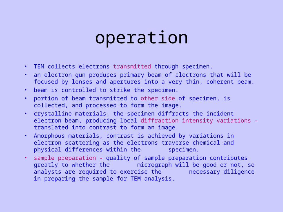
operation
• TEM collects electrons transmitted through specimen. • an electron gun produces primary beam of electrons that will be focused by
lenses and apertures into a very thin, coherent beam.• beam is controlled to strike the specimen. • portion of beam transmitted to other side of specimen, is collected, and
processed to form the image. • crystalline materials, the specimen diffracts the incident electron beam,
producing local diffraction intensity variations - translated into contrast to form an image.
• Amorphous materials, contrast is achieved by variations in electron scattering as the electrons traverse chemical and physical differences within the specimen.
• sample preparation - quality of sample preparation contributes greatly to whether the micrograph will be good or not, so analysts are required to exercise the necessary diligence in preparing the sample for TEM analysis.

QuickTime™ and aTIFF (Uncompressed) decompressor
are needed to see this picture.


QuickTime™ and aTIFF (Uncompressed) decompressor
are needed to see this picture.

references• http://www.sonix.com/learning/applications.php3• http://www.acoustech-inc.com/examples.asp• http://www.colorado.edu/physics/2000/xray/making_xrays.html• http://www.qualitydigest.com/dec99/html/semifig1.html• http://www.azom.com/details.asp?ArticleID=2673• http://www.mats-uk.com/techniques/techniques.html#tofsims• http://www.nanoscience.gatech.edu/zlwang/research/tem.html• W.R. Runyan and T.J Shaffner, “Semiconductor
Measurementss & Instrumentation”, 2nd edn.McGraw Hill.(QC611.24 R943)