fast switching fractional-n frequency synthesizer...
TRANSCRIPT
Int. J. Communications, Network and System Sciences, 2009, 2, 879-887 doi:10.4236/ijcns.2009.29102 Published Online December 2009 (http://www.SciRP.org/journal/ijcns/).
Copyright © 2009 SciRes. IJCNS
879
Fast Switching Fractional-N Frequency Synthesizer Architecture Using TDTL
Mahmoud A. AL-QUTAYRI, Saleh R. AL-ARAJI, Abdulrahman Al-HUMAIDAN College of Engineering, Khalifa University of Science, Technology and Research, Sharjah, UAE
E-mail:{mqutayri, alarajis}@kustar.ac.ae, [email protected] Received July 30, 2009; revised August 2, 2009; accept September 19, 2009
ABSTRACT This paper presents an efficient indirect fractional frequency synthesizer architecture based on the time delay digital tanlock loop. The indirect type frequency synthesis systems incorporate a low complexity high per-formance adaptation mechanism that enables them to remain in a locked state following the division process. The performance of the proposed fractional-N synthesizer under various input conditions is demonstrated. This includes sudden changes in the system input frequency as well as the injection of noise. The results of the extensive set of tests indicate that the fractional-N synthesizer, proposed in this work, performs well and is capable of achieving frequency divisions with fine resolution. The indirect frequency synthesizer also has a wide locking range and fast switching response. This is reflected by the system ability to regain its lock in response to relatively large variations in the input frequency within a few samples. The overall system per-formance shows high resilience to noise as reflected by the mean square error results. Keywords: Fractional, Synthesizer, Time Delay Tanlock Loop, Register Adaptation 1. Introduction Frequency synthesizers, particularly the fractional type, are a fundamental component of the many types of mod-ern wireless communication systems in use now a day. These complex wireless systems, be it for the ever grow- ing mobile communications market or other applications, need to support a multitude of different wireless stan-dards for disparate applications with their own data transfer requirements. However, irrespective of the wire-less standard in use, the data to be transferred will somehow need to be modulated on a radio frequency (RF) carrier, and the modulated signal is then transmitted over the air, and received and demodulated at the receiving end. At both the transmitting and the receiving end, an accurate RF carrier signal must be generated. Therefore, a radio frequency synthesizer is always required in order to perform frequency translation and channel selection [1–5].
The design of frequency synthesizers continues to pre-sent major challenges due to the stringent RF require-ments as well as the demands for high speed in digital transceivers supporting the drive for convergence. Con-ventional frequency synthesis techniques [1,2] in use today may be broadly classified into the following types:
- Phase-locked loop (PLL) based, or ‘indirect’
- Mixer / filter / divide, or ‘direct analog’ - Direct digital synthesis (DDS) Each of these methodologies has its merits and limita-
tions. Direct analog synthesis uses the functional ele-ments of multiplication, division and other mathematical manipulation to produce the desired frequency, but this method is a very expensive one. DDS uses logic and memory elements to digitally construct the desired out-put signal. On the output side, a digital-to-analog (D/A) converter is used to convert the digital signal to analog domain. The main limitations of DDS are the limited bandwidth and spurious harmonic generation. PLL- based frequency synthesis has been widely used in in-dustry. However, one of the major difficulties associated with the PLL-based technique is that a PLL with a wide frequency range cannot be achieved easily. In addition, fast switching is difficult to achieve. Typically, the out-put frequency step size of this method is the reference frequency. With fractional-N synthesis technique, finer frequency control can be achieved; however, these sys-tems typically have very narrow bandwidth [7–10].
Today’s advanced communication systems demand frequency synthesizers of high resolution, wide band-width and fast switching speed. The fractional frequency synthesizer proposed in this paper is designed to achieve the above mentioned requirements. It is of the indirect

M. A. AL-QUTAYRI ET AL.
Copyright © 2009 SciRes. IJCNS
880
Figure 1. Architecture of time-delay digital tanlock loop.
type that uses time delay digital tanlock loop (TDTL) as the phase locking element, a divider, and an efficient adaptive control structure.
The paper is organized as follows. Section 2 presents the architecture and system equations of the time-delay digital tanlock loop. This also includes the locking range of the TDTL which is a major aspect of a phase lock loop. Section 3 discusses the process and the challenges of using the TDTL as a frequency synthesizer. The ad-aptation process introduced to enable the TDTL based frequency synthesizer to achieve locking for the frac-tional frequency division is detailed in Section 4. The results of the new TDTL based fractional frequency syn-thesizer (TDTL-FFS) for various division factors and under different input conditions are detailed in Section 5. An assessment of the performance of the TDTL-FFS is presented in Section 6. The conclusions of this work are presented in Section 7. 2. TDTL Architecture and System Equations The architecture of the TDTL is shown in Figure 1. It consists mainly of two samples and hold blocks, a phase detector, a low pass filter, a digitally controlled oscillator, and a time-delay block [11]. Being comprised of these components, the TDTL lends itself for implementation in various digital systems technologies. The TDTL offers an inexpensive implementation and improved perform-ance compared with other synchronization techniques. Compared with the conventional digital tanlock loop in [12], the TDTL in Figure 1 does not preserve the linear-ity of the phase characteristics due to the existence of input dependant phase shift caused by the time delay. However, this disadvantage is considered relatively mi-nor due to the significant advantages offered by the TDTL, which include wider locking range and fast ac-quisition behavior. An in depth comparison of the con-ventional digital tanlock loop and TDTL with extensive
results and discussion is given in [13]. The mathematical analysis of the TDTL under noise free conditions is de-tailed below. All of the signal notations are chosen in reference to the block diagram shown in Figure 1. The analysis follows a similar line to that given in [13,14].
The TDTL receives a continuous time sinusoid y(t) which is given by (1).
[ ] )()(sin)( tnttAty o ++= θω (1)
where A is the amplitude of the signal, ω0 is the free run-ning frequency of the DCO, θ(t)=(ω-ω0)t+θ0 is the in-formation-bearing phase and n(t) is the additive white Gaussian noise (AWGN). The signal is assumed not to have a DC component. Usually the phase process θ(t) is a translation of frequency or phase steps. ω is the radian frequency of the input signal and θ0 is a constant. A phase lag ψ=ωτ is induced to the input signal after it passes through the time delay block. Therefore, x(t) is generated, which is a phase shifted version of the input signal y(t), this signal is given by (2).
/( ) sin ( ) ( )ox t A t t n tω θ= + − Ψ + (2)
where n’(t) is the time-delayed AWGN due to τ. The aforementioned continuous time signals pass to the sam-ple and hold blocks, and thereby get transformed to the discrete time signals in (3) and (4).
[ ] )()()(sin)( knkktAky o ++= θω (3) /( ) sin ( ) ( ) ( )ox k A t k k n kω θ= + − Ψ + (4)
where )]([)( ktk θθ = . The sampling interval between the sampling instants
t(k) and t(k-1) is given by (5). )1()( 0 −−=Τ kcTk (5)
where T0=2π/ω0 is the nominal period of the DCO and c(i) is the output of the digital filter at the ith sampling instant. Assuming t(0)=0, the total time t(k) elapsed up to the kth sampling instant is given by (6).

M. A. AL-QUTAYRI ET AL.
Copyright © 2009 SciRes. IJCNS
881
1
1 0
( ) ( ) ( )k k
oi i
t k T i kT c i−
= =
= = −∑ ∑ (6)
1
0
( ) sin ( ) ( ) ( )k
oi
y k A k c i n kθ ω−
=
= − +
∑ (7)
1/
0
( ) sin ( ) ( ) ( )k
oi
x k A k c i n kθ ω−
=
= − − Ψ +
∑ (8)
and therefore, the phase error between the input signal and the DCO can be also defined as:
1
0
( ) ( ) ( )k
oi
k k c iϕ θ ω−
=
= − − Ψ∑ (9)
Having defined the phase error, Equations (7) and (8) can be rewritten as
[ ] )()(sin)( / knkAky +Ψ+= φ (10)
[ ] )()(sin)( / knkAkx += φ (11)
These signals are applied to the phase detector pro-ducing the error signal e(k) given in (12).
[ ][ ] )(
)(sin)(sintan)( 1 k
kkfke ζ
φφ
+
Ψ+= − (12)
where [ ]ππγπγ 2mod)()( ++−=f , )(kζ is a random phase disturbance due to AWGN. The error signal e(k) represents a nonlinearly mapped version of the phase error. However, the effect of the nonlinearity is mini-mum and e(k) can be approximately linear if ψ is equal to, or in the vicinity of π/2. The digital filter, which has a transfer function given by D(z) receives the error signal e(k) and produces the signal c(k) that drives the DCO. Therefore, the system difference equation can be derived from (6) and (9) as
okckk Λ+−=+ )()()1( ωφφ (13)
where 000 /)(2 ωωωπ −=Λ , and the AWGN terms are neglected since noise-free analysis is assumed. In the case of the conventional digital tanlock loop, the linear characteristic function of the phase detector enables the description of the loop as a linear difference equation, and hence finding the lock range using the stability crite-rions of its Z-transformed transfer function [12]. How-ever, the nonlinear characteristic function of the TDTL phase detector results in a nonlinear difference equation, which can only be solved by numerical analysis. The lock range of the TDTL was analyzed in [11], using fixed-point theorems [15]. The digital filter of the first order loop is simply a gain block G1, and the system equation is given by
[ ] okhKkk Λ+−=+ )()()1( /1 φφφ (14)
where 1/
1 GK ω= . Defining K1 as ωoG1 will result in
WKK /1/1 = , where ωω /oW = . The nominal phase lag
Ψo induced by the time delay units on the input can be initially arranged by manipulating the parameters ωo and τ in the manner given by Ψo=ωτo. Therefore, the locking range can be acquired by numerically solving the in- equality
)sin()(sin)(sin212
22
1o
oWKWΨ
Ψ++<<−
αα (15)
where )(tan 1 βα −= , )cos()cot(
)(sin)tan()cos(1
)tan()sin(Ψ−
Ψ=
Ψ−Ψ
=ηη
ηβ
and /1KoΛ
=η
One of the properties of the first order TDTL is that it converges to a nonzero steady state phase error, which is translated with a phase offset between the pulses of the DCO and the zero crossings of the input signal. The steady-state value of the phase error is given by
πσφ jss += where { }1,0,1 −∈j . Figure 2 shows the lock-ing range of the first-order TDTL for different values of Ψo as well as the conventional digital tanlock loop lock-ing region [11]. Note that the region enclosed by (1), (2) and (3) is for the conventional digital tanlock loop; the region enclosed by (1), (2) and (4) is for the TDTL when Ψ0=π⁄2; and the region enclosed by (1) and (5) is for the TDTL when Ψ0=π.
The range of independent locking of the TDTL and the effect of initial phase error are studied in depth in [11, 13]. Since the TDTL has non-linear characteristic func-tion numerical analysis were used to determine the range of independent locking. The analysis shows that the TDTL offers an advantage on the conventional digital tanlock loop in this regard.
Figure 2. Major locking range of the first-order TDTL for different values of Ψ0=ω0τ.

M. A. AL-QUTAYRI ET AL.
Copyright © 2009 SciRes. IJCNS
882
Figure 3. Basic architecture of TDTL-based frequency synthesizer. 3. TDTL-Based Frequency Synthesizer
Architecture In order to utilize the TDTL system, described in the previous section, for indirect frequency synthesis the original system architecture needs to be modified as shown in Figure 3. The additional block in Figure 3 is a composite frequency divider with adaptation control mechanism. This is slightly more involved than a con-ventional indirect phase lock loop based synthesizer, which would normally only include a divider in its basic form. However, in the TDTL-based frequency synthe-sizer (TDTL-FS) structure in Figure 3 the adaptation mechanism is essential for the proper operation and sta-bility of the system, as explained below. Once the system operates correctly it results in dividing the DCO output frequency by the desired factor specified by the compos-ite divider block.
The necessity to incorporate an adaptation mechanism is dictated by the direct bearing that a divider block, after the DCO, has on the overall locking state of the TDTL-FS. If the system parameters of the original TDTL in Figure 1, without the divider, are selected such that it operates at optimum point “A” within the first-order loop locking range depicted in Figure 4, then such a system will have a stable behavior, within bounds, as demon-strated by the results in Section 4 as well as in [14]. However, it was observed that the moment a division of the TDTL DCO output frequency is attempted the com-plete system gets driven out to a point outside the lock range, such as point “B”, of Figure 4. Once the system moves to such points outside the lock range, it will be in an unstable state and hence cannot be used. The reason for this is that the divider block affects both the DCO free running frequency and the error signal at the input of the digital filter block. Both of these parameters have direct effect on the system locking.
Therefore, incorporating an adaptation mechanism with the divider in Figure 3 is necessary to overcome the critical locking problem outlined above. It is to be noted that point “A” in Figure 4, at which W=1and K1=1, is considered an optimum point within the lock range of the first-order TDTL with π/2 delay, because it allows for maximum symmetrical variation in both the input fre-quency and the loop gain while maintaining the system locked state. In this study it is always assumed that the loop is operating at this point prior to switching the di-vider for frequency synthesis. 4. TDTL Fractional-N Frequency Synthesizer The complete block diagram of the TDTL-FFS is de-picted in Figure 5. In addition to the TDTL, the system includes a fractional divider block that uses the pre- sca-ler technique, and an efficient adaptation mechanism that utilizes registers in order to maintain coherence between the input signal frequency (fref) and the divider output frequency (fs). As the TDTL-FFS involves multiple divi-sions, fast system response that counteracts the effect of the division and keeps the complete system in lock is highly desirable.
0 0.5 1 1.5 2 2.50
0.5
1
1.5
2
2.5
3
3.5
4
4.5
5
Frequency ratio, W = ωo / ω
Loop
gai
n, K
1 =
G ω
o
A
B
Figure 4. Lock range of 1st order TDTL with π/2 delay.
M. A. AL-QUTAYRI ET AL.
Copyright © 2009 SciRes. IJCNS
883
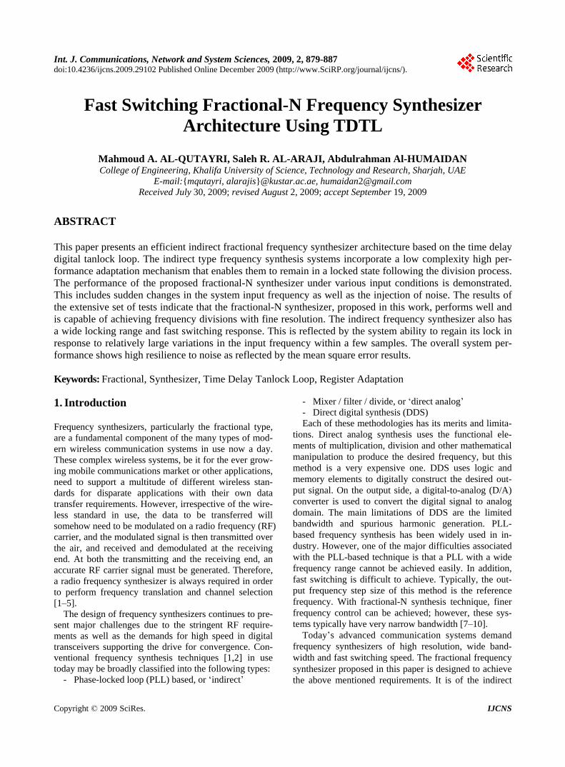
Figure 5. TDTL-FFS with register adaptation.
In the TDTL-FFS in Figure 5, the output frequency
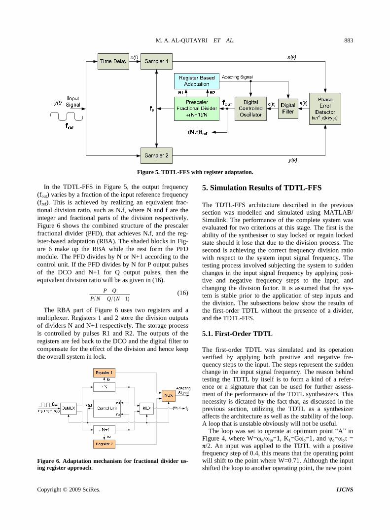
(fout) varies by a fraction of the input reference frequency (fref). This is achieved by realizing an equivalent frac-tional division ratio, such as N.f, where N and f are the integer and fractional parts of the division respectively. Figure 6 shows the combined structure of the prescaler fractional divider (PFD), that achieves N.f, and the reg-ister-based adaptation (RBA). The shaded blocks in Fig-ure 6 make up the RBA while the rest form the PFD module. The PFD divides by N or N+1 according to the control unit. If the PFD divides by N for P output pulses of the DCO and N+1 for Q output pulses, then the equivalent division ratio will be as given in (16).
( 1)P Q
P N Q N+
+ + (16)
The RBA part of Figure 6 uses two registers and a multiplexer. Registers 1 and 2 store the division outputs of dividers N and N+1 respectively. The storage process is controlled by pulses R1 and R2. The outputs of the registers are fed back to the DCO and the digital filter to compensate for the effect of the division and hence keep the overall system in lock.
Figure 6. Adaptation mechanism for fractional divider us-ing register approach.
5. Simulation Results of TDTL-FFS The TDTL-FFS architecture described in the previous section was modelled and simulated using MATLAB/ Simulink. The performance of the complete system was evaluated for two criterions at this stage. The first is the ability of the synthesiser to stay locked or regain locked state should it lose that due to the division process. The second is achieving the correct frequency division ratio with respect to the system input signal frequency. The testing process involved subjecting the system to sudden changes in the input signal frequency by applying posi-tive and negative frequency steps to the input, and changing the division factor. It is assumed that the sys-tem is stable prior to the application of step inputs and the division. The subsections below show the results of the first-order TDTL without the presence of a divider, and the TDTL-FFS. 5.1. First-Order TDTL The first-order TDTL was simulated and its operation verified by applying both positive and negative fre-quency steps to the input. The steps represent the sudden change in the input signal frequency. The reason behind testing the TDTL by itself is to form a kind of a refer-ence or a signature that can be used for further assess-ment of the performance of the TDTL synthesizers. This necessity is dictated by the fact that, as discussed in the previous section, utilizing the TDTL as a synthesizer affects the architecture as well as the stability of the loop. A loop that is unstable obviously will not be useful.
The loop was set to operate at optimum point “A” in Figure 4, where W=ωo/ωin=1, K1=Gωo=1, and ψo=ωoτ = π/2. An input was applied to the TDTL with a positive frequency step of 0.4, this means that the operating point will shift to the point where W=0.71. Although the input shifted the loop to another operating point, the new point

M. A. AL-QUTAYRI ET AL.
Copyright © 2009 SciRes. IJCNS
884
is still within the locking range of the loop. Hence, the loop did not go out of lock and stabilized indicating that the loop has locked onto the new frequency. However, the TDTL response does not converge to zero error in the steady state due to the limitations of the first order loop. The limitation is an inherent feature of the first-order TDTL because the filter block in Figure 1 is only a gain block of G. The response of the system to a positive fre-quency step is shown in Figure 7. The error signal or the system response is taken from the output of the phase error detector. The result of applying a negative fre-quency step is shown in Figure 8. In this case W=1.42, but the system manages to stabilize and converge to none-zero steady state error. 5.2. Fractional-N TDTL Frequency Synthesizer The performance of the fractional-N TDTL frequency synthesizer architecture with register based adaptation mechanism, as described in Section 3, was evaluated
(a)
(b)
Figure 7. TDTL response to a positive frequency step of 0.4. (a) Frequency step input; (b) Output of the phase error detector.
(a)
(b)
Figure 8. TDTL response to a negative frequency step. (a) Frequency step input; (b) Output of the phase error detector.
through an extensive set of tests. The tests were primar-ily concerned with assessing the ability of the TDTL- FFS, which includes the composite divider block, to re-main in lock following the division of the DCO output frequency and achieve various frequency division ratios.
The extensive tests conducted on the TDTL-FFS indi-cate that it performs very well with respect to the evalua-tion criterions stated above. This section details some of the results that were achieved. In all the test cases it is assumed that the basic TDTL parameters were selected so that it operates at the optimum point within the lock-ing range of Figure 4 prior to the activation of the com-posite divider block that converter the system to a TDTL-FFS. It is also assumed that sudden changes in the input signal frequency are not severe so as to drive the system out of lock. These assumptions are applied in order to focus on proving that the new architecture is capable of performing fractional frequency synthesis. TDTL system architectures that deal with wide variations in the input signal frequency through extended locking range are discussed in [13,14].
The importance and effectiveness of the register based adaptation mechanism of the composite divider block of the TDTL-FFS is illustrated in Figure 9. In this case the TDTL-FFS was subjected to the positive frequency step in Figure 7(a) and a pre-scaler divider block with a divi-sion ration of 4 and no adaptation was included at the DCO output. Figure 9(a) shows that the system lost its locked state. This is further illustrated by the phase plane plot depicted in Figure 9(b). Replacing the divider block with one that also includes the register adaptation ele-ments enabled the TDTL-FFS system to regain its locked for the same positive step frequency input as shown in Figure 9(c).
The effect of a division ration of 3.5 and a positive step input, the same one in Figure 7(a), is illustrated in Figure 10. The figure shows the DCO output as well as the divider output which clearly indicates the impact of the division.
The response of the TDTL-FFS to a negative fre-quency step and a division ratio of 3.8 are illustrated in Figure 11 and Figure 12 respectively. The output of the phase error detector in Figure 11 indicates that the sys-tem regain locking following the application of the nega-tive step within a relatively small number of samples. The fractional divider output in Figure 12 indicates a frequency that is 3.8 with respect to that of the DCO output.
In many applications, such as adjacent cells of a wire-less network, fine divisions are required. The ability of the TDTL-FFS to achieve such fine fractional division ratios is demonstrated in Figure 13. The division ratio at output of the divider block with respect to the DCO out-put is 2.0714285. The TDTL-FFS was also tested for other division factors and input frequency steps. The system behaved consistently by achieving the required divisions provided that the assumptions stated earlier are maintained.

M. A. AL-QUTAYRI ET AL.
Copyright © 2009 SciRes. IJCNS
885
0 5 10 15 20 25 30 35 40-0.4
-0.3
-0.2
-0.1
0
0.1
0.2
0.3
0.4
0.5
Time
Pha
se E
rror
(a)
-3 -2 -1 0 1 2 3 4-3
-2
-1
0
1
2
3
4
φ(K)rad
φ(K
+1)ra
d
φ(0)
(b)
(c)
Figure 9. TDTL-FFS response to a positive step. (a) With-out adaptation; (b) Phase plane without adaptation; (c) Response with adaptation.
(a)
(b)
Figure 10. TDTL-FFS outputs for 3.5 division factor. (a) DCO output; (b) Frequency divider output.
Figure 11. TDTL-FFS system response to a negative fre-quency step with RBA. (a) Frequency step input; (b) Phase error detector output.
Figure 12. TDTL-FFS outputs for 3.8 division factor. (a) DCO output; (b) Frequency divider output.
15 16 17 18 19 20 21 22 23 24 25-0.5
0
0.5
1
Time (a)
DC
O o
utpu
t
15 16 17 18 19 20 21 22 23 24 25 -0.5
0
0.5
1
Time (b)
Div
ider
out
put
0 5 10 15 20 25 30 35 40-0.5
-0.4
-0.3
-0.2
-0.1
0
0.1 0.2 0.3 0.4 0.5
Time
Phas
e Er
ror
0 5 10 15 20 25 30 35 40-0.4
-0.3
-0.2
-0.1
0
Time (a)
Freq
uenc
y st
ep
0 5 10 15 20 25 30 35 40
-0.4
-0.2
0 0.2 0.4 0.6
Time (b)
Erro
r sig
nal

M. A. AL-QUTAYRI ET AL.
Copyright © 2009 SciRes. IJCNS
886
0 5 10 15 20 25 30 35 40-0.5
0
0.5
1
1.5
DC
O O
utpu
t
(a)
0 5 10 15 20 25 30 35 40-0.5
0
0.5
1
1.5
DC
O O
utpu
t
(b)
Figure 13. TDTL-FFS outputs for 2.0714285 division factor. (a) DCO output; (b) Frequency divider output.
0.00E+00
2.00E-02
4.00E-02
6.00E-02
8.00E-02
1.00E-01
1.20E-01
0.1 0.2 0.3 0.4 0.5
MSE
Frequency Step
With Noise
Without Noise
Figure 14. Relationship between frequency step and MSE.
6. TDTL-FFS Speed and Noise Performance Section 5 above demonstrated the ability of the TDTL- FFS to perform fractional division while maintain the state of locking. Extensive set of test showed that the TDTL-FFS is able to stay in lock when the input fre-quency varies over a wide range. This is a highly desir-able feature of frequency synthesizers as it gives the de-vice the ability to support a variety of wireless commu-nication standards that will invariably operate at different frequencies.
The simulation results of the TDTL-FFS also show clearly that the device support fast switching. The vari-ous plots of the synthesizer response, for positive as well as negative input frequency steps, show that the system settles to steady state within a few samples. This was achieved for a variety of division factors including very fine ones. This characteristic of the TDTL-FFS makes it useful in wireless networks with frequency hopping re-quirements. The performance of the TDTL-FFS under noise conditions was also evaluated. This was done by
measuring the mean square error (MSE) for various fre-quency steps under both noise free and noisy conditions. The plots in Figure 14 illustrate the resilience of the TDTL-FFS to noise. The system kept its locked state and the increase in MSE as a result of the injection of noise is acceptable. A similar study was also conducted to evalu-ate the effect of noise at different division ratios. The results also indicated that the TDTL-FFS performs very well under noisy conditions. 7. Conclusions This paper presented a novel fractional frequency syn-thesizer architecture based on the TDTL. A major chal-lenged faced in utilizing the TDTL for frequency synthe-sis is keeping the system in locked state following the division process. This problem was overcome by includ-ing an adaptation block that compensated for the effects the division had on the loop. The compensation mecha-nism is an efficient one as it has low complexity and en-ables fast locking.
The composite adaptor divider block in the TDTL-FFS consisted of a pre-scaler divider and a register based ad-aptation mechanism. The registers utilize the division information to force the complete system to operate within the locking region by controlling the loop filter gain and the DCO.
The results showed that the TDTL-FFS is capable of performing fractional-N divisions with fine resolution. It can also deal with both positive and negative frequency steps over a wide range of frequencies. The TDTL-FFS has fast switching capabilities and high resilience to noise.
8. References
[1] R. Staszewski and P. Balsara, “All-digital frequency syn-
thesizer in deep-submicron CMOS,” Wiley, 2006. [2] A. Lacaita, S. Levantino, and C. Samori, “Integrated fre-
quency synthesizers for wireless systems,” Cambridge University Press, 2007.
[3] C. Mishra, et al., “Frequency planning and synthesizer architectures for multiband OFDM UWB radios,” IEEE Transactions on Microwave Theory and Techniques, Vol. 53, pp. 3744–3756, December 2005.
[4] C. Gaudes, M. Valkama, and M. Renfors, “A novel fre-quency synthesizer concept for wireless communica-tions,” Proceings of International Symposium Circuits and Systems (ISCAS), Vol. 2, pp. 85–88, 2003.
[5] T. Lin, J. Kaiser, and J. Pottie, “Integrated low-power communication system design for wireless sensor net-works,” IEEE Communication Magazine, Vol. 42, pp. 142–150, December 2004.
[6] F. Agnelli, et al., “Wireless multi-standard terminals:

M. A. AL-QUTAYRI ET AL.
Copyright © 2009 SciRes. IJCNS
887
System analysis and design of a reconfigurable RF front-end,” IEEE Circuits and Systems Magazine, Vol. 6, pp. 38–59, 2006.
[7] A. Chenakin, “Frequency synthesis: Current solutions and new trends,” Microwave Journal, Vol. 50, pp. 256–260, May 2007.
[8] S. Moon, A. Valero-Lopez, and E. Sanchez-Sinencio, “Fully integrated frequency synthesizer: A tutrial,” Inter-national Journal High Speed Electronics and Systems, Vol. 15, pp. 353–375, June 2005.
[9] J. Vankka, “Digital synthesizers and transmitters for soft-ware radio,” Springer, 2005
[10] A. Bellaouar, M. O'brecht, M. Fahim, and M. Elmasry, “Lowpower direct digital frequency synthesis for wireless communications,” IEEE Journal of Solid-State Circuits, Vol. 35, pp. 385–390, March 2000.
[11] Z. Hussain, B. Boashash, M. Hassan-Ali, and S. Al-Araji, “A time-delay digital tanlock loop,” IEEE Transactions
on Signal Processing, Vol. 49, No. 8, pp. 1808–1815, 2001.
[12] C. Lee and C. K. Un, “Performance analysis of digital tanlock loop,” IEEE Transactions on Communications, Vol. COM-30, pp. 2398–2411, October 1982.
[13] S. R. Al-Araji, Z. M. Hussain, and M. A. Al-Qutayri, “Digital phase lock loops: Architectures and applica-tions,” Springer, 2006.
[14] M. Al-Qutayri, S. Al-Araji, and N. Al-Moosa, “Improved first-order time-delay tanlock loop architectures,” IEEE Transactions on Circuits and Systems Part-I, Vol. 53, No. 9, pp. 1896–1908, 2006.
[15] A. Granas and J. Dugundji, “Fixed point theorem,” Springer, 2003.
[16] A. Al-Humaidan, S. Al-Araji, and M. Al-Qutayri, “Fre-quency synthesizer for wireless applications using TDTL,” IEEE APCCAS, pp. 1518–1521, December 2006.