far-field wireless power transmission: rf, signal and ... · far-field wireless power transmission:...
TRANSCRIPT

Far-Field Wireless Power Transmission: RF, Signal
and System Designs
Bruno Clerckx and Paul Mitcheson
Dept. of Electrical and Electronic EngineeringImperial College London
EuCAP 2018, London
1 / 84

Contents
1 WPT: Introduction and Applications
2 RF, Signal and System Design for WPT
3 Conclusions and Future Challenges
2 / 84

WPT and WIPT: Introduction and Applications
1 WPT: Introduction and ApplicationsWireless is More than Just CommunicationsWhy Wireless Power?Wireless Power via RFWireless Information and Power Transfer
2 RF, Signal and System Design for WPT
3 Conclusions and Future Challenges
3 / 84

Wireless is More than just Communications
4 / 84

In 20 Years from Now ... Trillions of Low-Power Devices
5 / 84

Why Wireless Power?
Wireless Power Transfer (WPT): deliver power wirelessly (without wires)
Benefits
• No wires, no contacts (it travels through walls), no (or at least reduced)batteries• A perpetual, predictable, dedicated, on-demand and reliable energy supply
as opposed to ambient energy-harvesting technologies such as solar,thermal, or vibration• Smaller, lighter and compact devices• No production/maintenance/disposal of trillions of batteries• Prolonged lifetime of devices
Applications
• Networks with ubiquitous/autonomous low-power/energy-limited devices• Consumer electronics wireless charging• Biomedical implants wireless charging• Wireless sensor/IoT devices charging• Simultaneous wireless information and power transfer (SWIPT)• Wirelessly powered communication networks (WPCNs)• Wirelessly powered backscatter communication (WPBC), e.g. RFID
6 / 84

Comparison of the main technologies for WPT
Technology Devices Range Frequency Pros/ConsInductivecoupling
Wire coils Millimeterstocentimeters
Hz to MHz High efficiency, require precise tx/rxcoil alignment, very short range,single receiver only
Magneticresonantcoupling
Tuned wirecoils, lumpedelementresonators
A fewmeters,typically 4 to10 times thecoil diameter
kHz to MHz High efficiency, safe, mid-range,large tx/rx size
EM radiation Dishantenna,antennaarray,rectenna
Severalmeters tohundreds ofkilometers
MHz todozens ofGHz
Long range, small receiver formfactors, flexible in deployment andmovement, support power multicas-ting, potential for SWIPT, LoS linkis not a must, low efficiency, safetyand health issues
Laser powerbeaming
Laseremitter,photovoltaicreceiver
up tokilometers
THz Compact size, high energy concen-tration, no interference to exist-ing communication systems or elec-tronics, laser radiation is hazardous,require LoS link and accurate re-ceiver targeting, vulnerable to at-mospheric absorption and scatter-ing by clouds, fog, and rain
Focus in this tutorial is on WPT with EM radiation
7 / 84
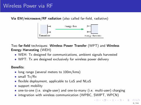
Wireless Power via RF
Via EM/microwave/RF radiation (also called far-field, radiative)
Two far-field techniques: Wireless Power Transfer (WPT) and WirelessEnergy Harvesting (WEH)
• WEH: Tx designed for communications, ambient signals harvested
• WPT: Tx are designed exclusively for wireless power delivery
Benefits:
• long range (several meters to 100m/kms)
• small Tx/Rx
• flexible deployment, applicable to LoS and NLoS
• support mobility
• one-to-one (i.e. single-user) and one-to-many (i.e. multi-user) charging
• integration with wireless communication (WPBC, SWIPT, WPCN)
8 / 84

Wireless Power via RF
PT PR
WPT with co-located antennas
one-to-one
PT
PR
PR
PR
WPT with co-located antennas
one-to-many
Energy flow
PT
PT
PT
PR
PR
WPT with distributed antennas
P T/R: Power Transmitter/Receiver
PT+IT PR+IR
SWIPT with co-located receivers
PT+IT PR
IR
SWIPT with separated receivers
PT+IR PR+IT
WPCN
Energy flow
Information flow
Tag
RF Tx
Reader
WPBC
P/I T/R: Power/Information Transmitter/Receiver
9 / 84

Wireless Power via RF
Limitations: low efficiency, safety and health issues
• WiFi: 5.18GHz, 36dBm (4W ) Tx power, 2dBi Rx antenna gain, 58dB pathloss (i.e. office) → Rx power before conversion of about -20dBm (10µW )
Applications: Wireless charging for
• low-power devices: RFID tags, wireless sensors/IoT devices,
• consumer electronics: smart phones, laptops, household robots, ...
• high-power: microwave-powered aircrafts, solar power satellite (SPS)
Industry standard: pretty much 0G (RFID only?)
Companies: Intel, Energous, PowerCast, Ossia, Drayson Technologies,...
10 / 84

Wireless Information and Power Transfer
PT+IT PR+IR
SWIPT with co-located receivers
PT+IT PR
IR
SWIPT with separated receivers
PT+IR PR+IT
WPCN
Energy flow
Information flow
Tag
RF Tx
Reader
WPBC
P/I T/R: Power/Information Transmitter/Receiver
Various forms of Wireless Information and Power Transfer:
• Simultaneous Wireless Information and Power Transfer (SWIPT): DLWPT and WIT at the same time
• Wirelessly Powered Communication Networks (WPCNs): DL WPT andUL wireless information transmission (WIT)
• Wirelessly Powered Backscatter Communication (WPBC): backscatteringmodulation at the tag to reflect and modulate the incoming RF signal forcommunication with a reader
11 / 84

Wireless Information and Power Transfer
... applications in all usual communication channels
Figure: Point-to-point
Figure: Interference Channel
ID user
EH user
ID user
ID user
1
| |S
i
ID userIDK
EH user
EH user
1
j
EHK
1h
| |Sh
ih
1g
jg
EHKg
Figure: Broadcast Channel
Figure: Relay Channel
12 / 84

RF, Signal and System Design for WPT
1 WPT: Introduction and Applications
2 RF, Signal and System Design for WPTWPT ArchitectureRectenna DesignTowards WPT Signal DesignSingle-User WPT Signal DesignMulti-User WPT Signal DesignChannel Acquisition for WPTPrototyping and Experimentation of Closed-Loop WPT
3 Conclusions and Future Challenges
13 / 84

Past and Present
Historical WPT:
• Targeting for long distance and high power (e.g., 450kW)
• Mainly driven by the wireless-powered aircraft and SPS applications
• Requires high transmission power, huge Tx/Rx antennas (e.g., 26-mdiameter parabolic dish), clear LoS
Modern WPT:
• Low-power (e.g., from µW to a few W ) delivery over moderate distances(e.g., from a few m to possibly hundreds of m)
• Need to build reliable and convenient WPT systems for remotely chargingvarious low- to medium-power devices (RFID tags, wireless sensors, smartphones, ...)
14 / 84

New Design Challenges and Requirements
1 Range: Deliver wireless power at distances of 5-100m for indoor/outdoorcharging of low-power devices.
2 Efficiency: Boost the end-to-end power transfer efficiency (up to a fractionof percent/a few percent).
3 Non-line of sight (NLoS): Support LoS and NLoS to widen the practicalapplications of this network.
4 Mobility support: Support mobile receivers, at least for those at pedestrianspeed.
5 Ubiquitous accessibility: Support ubiquitous power accessibility within thenetwork coverage area.
6 Seamless integration of wireless communication and wireless power:Interoperate wireless communication and wireless power via a unifiedwireless information and power transfer (WIPT).
7 Safety and health: Resolve the safety and health issues of RF systems andcomply with the regulations.
8 Energy consumption: Limit the energy consumption of theenergy-constrained RF powered devices.
15 / 84

WPT Architecture
A generic architecture
Energy
Transmitter
Energy
Receiver
Wireless
Channeldc
tP
rf
tP rf
rP dc
rP
End-to-End Power Transfer Efficiency
e =P rdcP tdc
=P trfP tdc︸︷︷︸
e1
P rrfP trf︸︷︷︸
e2
P rdcP rrf︸︷︷︸
e3
• WEH: no control of e1 and e2. Unlikely sufficient for powering deviceswith a few cm2 in size requiring 10-100µW
• WPT: more control of the design and room for enhancement of e
16 / 84

WPT Architecture
... slightly more detailed
RF
source
Power Transm
Tx
antenna(s)
Rx
antenna
network
Rectifier
converter Storage
Pdc,ST
End-to-End Power Transfer Efficiency: e =Pdc,ST
P tdc
=P trfP tdc︸︷︷︸
e1
P rrfP trf︸︷︷︸
e2
P rdcP rrf︸︷︷︸
e3
Pdc,ST
P rdc︸ ︷︷ ︸
e4
DC-to-RF conversion efficiency e1: efficient power amplifier (PA) design andtransmit signals with constrained PAPR
RF-to-RF conversion efficiency e2: directional transmission
• RF literature: time-modulated arrays based on localization of the powerreceivers, phased-arrays, retrodirective arrays
• Comms literature: multi-antenna beamforming and accurate channelknowledge at Tx
17 / 84

WPT Architecture
RF-to-DC conversion efficiency e3: rectenna design
• Antenna + Rectifier (a non-linear device + a low-pass filter and load)
• Assuming P trf = 1W , 5-dBi Tx/Rx antenna gain, a continuous wave (CW)at 915MHz, e3 ≈ 50% (1m), 25% (10m), 5% (30m)
• With CW, e3 ≈ 80% (10mW ), 40% (100µW ), 20% (10µW ), 2% (1µW )
• For input power 1µW -1mW , low barrier Schottky diodes preferred
• Single diode at 1-500µW and multiple diodes above 500µW
18 / 84

WPT Architecture
RF-to-DC conversion efficiency e3: waveform and modulation design
• Due to rectifier nonlinearity, e3influenced by input waveformpower and shape in the low inputpower regime (1µW -1mW )!
Time
0s 0.05us 0.10us 0.15us 0.20us 0.25us 0.30us 0.35us 0.40us 0.45us 0.50us 0.55us 0.60us 0.65us 0.70us 0.75us 0.80us 0.85us 0.90us 0.95us 1.00us
V(D1:1) V(R1:2)
-20V
-10V
0V
10V
20V
• Measurements have shown that 1) a multisine signal excitation enhancesthe output DC power and e3 over a CW signal (Trotter), 2) OFDM, whitenoise, chaotic waveforms with high PAPR increase e3 (Collado).
DC-to-DC conversion efficiency e4: dynamic tracking of rectifier optimum load19 / 84

WPT Architecture
Energy
Transmitter
Energy
Receiver
Wireless
Channeldc
tP
rf
tP rf
rP dc
rP
Careful! Maximizing e not achieved by maximizing e1, e2, e3, e4 independentlyfrom each other, and simply concatenating the above techniques
• e1, e2, e3, e4 coupled due to nonlinearity, especially at 1µW -1mW
• e3(input signal shape and power) → e3(Tx signal,wireless channel state)
• e2(Tx signal,wireless channel state)
• e1(Tx signal PAPR)
Notations: P trf often simply denoted as P in the sequel for simplicity
20 / 84

Rectenna Design
Rectenna Functions
London Underground RF Spectral Survey – Harvesting/Transfer
Wireless Power Receiver Design
What is the Design Strategy ?
Rectifier Topologies
Multi-Tone Wireless Power Receiver
21 / 84

Wireless Power Receiver (WPRx)Rectenna Design
Mahmoud Ouda, Paul D. Mitcheson, Bruno Clerckx
Far-Field Wireless Power Transmission: RF, Signal and System Designs, 2018 Mahmoud Ouda, Paul D. Mitcheson, B, Clerckx 1

Outline
• Rectenna Functions
• London Underground RF Spectral Survey –Harvesting/Transfer
• Wireless Power Receiver Design• Challenges
• Blocks
• What is the Design Strategy ?
• Rectifier Topologies
• Multi-Tone Wireless Power Receiver
Far-Field Wireless Power Transmission: RF, Signal and System Designs, 2018 Mahmoud Ouda, Paul D. Mitcheson, B, Clerckx 2

Rectenna Functions
Far-Field Wireless Power Transmission: RF, Signal and System Designs, 2018 Mahmoud Ouda, Paul D. Mitcheson, B, Clerckx 3
• Antenna + rectifier = Rectifying antenna (Rectenna)
• Picks up electromagnetic energy
• Converts it into dc power
• Stores it as an electrical energy
• Supplies dc voltage (power) to an electrical load.

How Good is Ambient RF?
Far-Field Wireless Power Transmission: RF, Signal and System Designs, 2018 Mahmoud Ouda, Paul D. Mitcheson, B, Clerckx 4
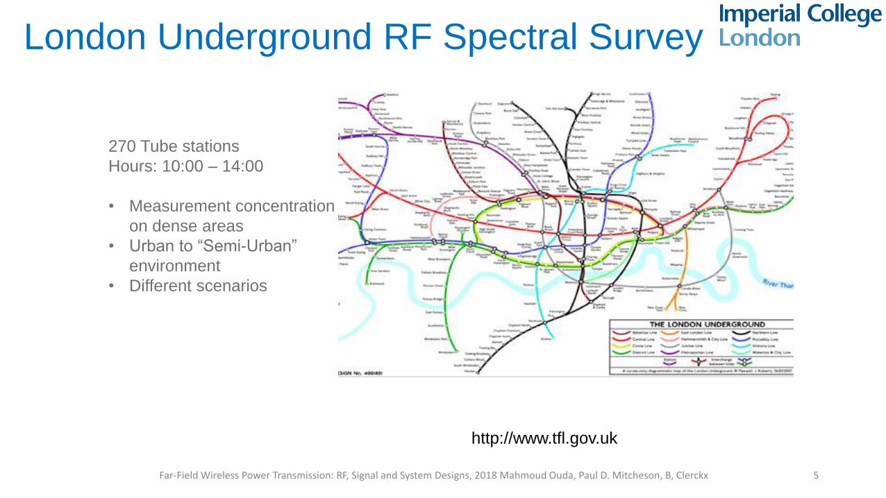
London Underground RF Spectral Survey
Far-Field Wireless Power Transmission: RF, Signal and System Designs, 2018 Mahmoud Ouda, Paul D. Mitcheson, B, Clerckx 5
270 Tube stations
Hours: 10:00 – 14:00
• Measurement concentration
on dense areas
• Urban to “Semi-Urban”
environment
• Different scenarios
http://www.tfl.gov.uk

Spectral Survey Equipment
Far-Field Wireless Power Transmission: RF, Signal and System Designs, 2018 Mahmoud Ouda, Paul D. Mitcheson, B, Clerckx 6
Agilent Fieldfox 0.03 - 6 GHz
Spectrum analyzer
Network analyzer
Cable and antenna analyzer
Aaronia Bicolog 20300
0.3-3 GHz calibrated omnidirectional
antenna.
296 calibration points, 10 MHz steps
Survey Procedure
Based on FCC, ECC and
ICNIRP standards
Max Hold
5 dB attenuation when
possible
20 dBµV/m reference level
“Panning approach”
Several sweeps in three axis
http://www.cept.org/ecc

London Underground RF Spectral Survey
Far-Field Wireless Power Transmission: RF, Signal and System Designs, 2018 Mahmoud Ouda, Paul D. Mitcheson, B, Clerckx 7
(Interactive website: www.londonrfsurvey.org/)

London Underground RF Spectral Survey
Far-Field Wireless Power Transmission: RF, Signal and System Designs, 2018 Mahmoud Ouda, Paul D. Mitcheson, B, Clerckx 8
GSM900
DTV
3G
WiFi
GSM1800

London Underground RF Spectral SurveySummary
Far-Field Wireless Power Transmission: RF, Signal and System Designs, 2018 Mahmoud Ouda, Paul D. Mitcheson, B, Clerckx 9
Band name Frequency (MHz) BW (MHz) Average P
(μW/cm2)
Maximum P
(μW/cm2)
DTV 470 - 610 140 0.89x10⁻³ 0.046
GSM 900 921 - 960 39 0.036 1.93
GSM 1800 1805 - 1876 71 0.084 6.39
WiFi 2400 - 2473 73 0.18x10⁻³ 6.47x10⁻³
3G 2110 - 2170 60 0.012 0.24

London Underground RF Spectral Survey
Far-Field Wireless Power Transmission: RF, Signal and System Designs, 2018 Mahmoud Ouda, Paul D. Mitcheson, B, Clerckx 10
(Interactive website : www.londonrfsurvey.org)

London Underground RF Spectral Survey
Far-Field Wireless Power Transmission: RF, Signal and System Designs, 2018 Mahmoud Ouda, Paul D. Mitcheson, B, Clerckx 11
(Interactive website : www.londonrfsurvey.org/)

WPT – Design Considerations
Far-Field Wireless Power Transmission: RF, Signal and System Designs, 2018 Mahmoud Ouda, Paul D. Mitcheson, B, Clerckx 12

WPT Challenges
• Very low power levels on antenna• Implies low voltage swing on diode• Difficulty in rectification• Thus a low efficiency
• Circuit is inherently non linear• Function of power level• Makes impedance match difficult• Analysis is tricky
• High frequency• Limits choice of diodes
Far-Field Wireless Power Transmission: RF, Signal and System Designs, 2018 Mahmoud Ouda, Paul D. Mitcheson, B, Clerckx 13

Block Diagram
Far-Field Wireless Power Transmission: RF, Signal and System Designs, 2018 Mahmoud Ouda, Paul D. Mitcheson, B, Clerckx 14

Block Diagram(1)
1. Antenna (Gr) Picks up electromagnetic (EM) energy
Generates RF voltage (VRF )
Specifications: Antenna gain (Gr) dBi (high could be good for WPT, but
bad for harvesting)
Impedance (Za) (not necessarily 50 W...)
Geometry (defines the system size)
Far-Field Wireless Power Transmission: RF, Signal and System Designs, 2018 Mahmoud Ouda, Paul D. Mitcheson, B, Clerckx 15
Storage
MatchingNetwork
RF-to-DCRectifier
DC-to-DCBoost

Block Diagram(2)
1. Antenna (Gr)
2. RF matching network Maximizes RF-power transfer to the converter
Conjugately matches the antenna/converter impedances
Boosts the RF voltage (VRF ) to turn on the next rectifying diode.
Needs to be low loss
Specifications:
Matching efficiency=(1-|Г|2) ; |Г| Reflection = |𝑍𝑖𝑛−𝑍𝑎
∗
𝑍𝑖𝑛+𝑍𝑎|
Far-Field Wireless Power Transmission: RF, Signal and System Designs, 2018 Mahmoud Ouda, Paul D. Mitcheson, B, Clerckx 16
Storage
MatchingNetwork
RF-to-DCRectifier
DC-to-DCBoost

Block Diagram(3)
Far-Field Wireless Power Transmission: RF, Signal and System Designs, 2018 Mahmoud Ouda, Paul D. Mitcheson, B, Clerckx 17
Storage
MatchingNetwork
RF-to-DCRectifier
DC-to-DCBoost
1. Antenna (Gr)
2. RF matching network
3. RF-to-dc power converter (Rectifier) Converts RF power into dc power
Nonlinear diode impedance with diode operating point (Vdiode, Idiode)
Function of input power PRF & loading condition RL(Vo)
Specifications:
RF-to-dc efficiency =𝑃𝑑𝑐
𝑃𝑅𝐹=
𝑃𝑑𝑐
𝑃𝑑𝑐+𝑃𝑙𝑜𝑠𝑠; 𝑃𝑙𝑜𝑠𝑠 = conduction and reverse leakage losses
PCE=𝑃𝑑𝑐
𝑃𝑑𝑐+𝑃𝑙𝑜𝑠𝑠

Block Diagram(4)
Far-Field Wireless Power Transmission: RF, Signal and System Designs, 2018 Mahmoud Ouda, Paul D. Mitcheson, B, Clerckx 18
Storage
MatchingNetwork
RF-to-DCRectifier
DC-to-DCBoost
1. Antenna (Gr)
2. RF matching network
3. RF-to-dc power converter (Rectifier)
4. DC-to-dc voltage boost converter Supplies a usable dc voltage level from low voltage RF-
DC stage Decouples the system load dynamics Could apply MPPT
Specifications: DC-to-dc efficiency = 𝑓(𝑉𝑖𝑛 = 𝑉𝑑𝑐)
Gr

What is the Design Strategy (1)?
Efficiency =𝑃𝑑𝑐
𝑃𝑖𝑛=
𝑃𝑑𝑐
𝑃𝑑𝑐+𝑃𝑙𝑜𝑠𝑠
Considering diode conduction loss:
Efficiency≈𝑉𝑑𝑐
𝑉𝑑𝑐+𝑉𝑑𝑖𝑜𝑑𝑒
where Vdiode ≈ 0.3 : 0.5 V
Target #1 : the highest possible Vdc out of the available input power, Pin
Far-Field Wireless Power Transmission: RF, Signal and System Designs, 2018 Mahmoud Ouda, Paul D. Mitcheson, B, Clerckx 19
Vdiode
VdcVin

What is the Design Strategy (2)?
Efficiency =𝑃𝑑𝑐
𝑃𝑖𝑛=
𝑃𝑑𝑐
𝑃𝑑𝑐+𝑃𝑙𝑜𝑠𝑠
Considering diode reverse loss:Vdiode rvs (= Vdc-Vin ) < VBD (for peak rectifier)
Vin peak should be < VBD/2 where VBD ≈ 2V (SMS7630)
To maintain the peak efficiency,
Target #1 : the highest possible Vdc out of the available input power, Pin
Target #2: Vdc should not breakdown the diode
Far-Field Wireless Power Transmission: RF, Signal and System Designs, 2018 Mahmoud Ouda, Paul D. Mitcheson, B, Clerckx 20
Vdiode
VdcVin

Optimal RF-to-dc efficiency
RF-to-dc efficiency =𝑃𝑑𝑐
𝑃𝑅𝐹=
𝑃𝑑𝑐
𝑃𝑑𝑐+𝑃𝑙𝑜𝑠𝑠;
𝑃𝑙𝑜𝑠𝑠 = 𝑃𝑓𝑤𝑑 + 𝑃𝑟𝑣𝑠 ;
The peak efficiency is an optimum between:
The forward (junction) loss
The reverse (breakdown) leakage loss.
Far-Field Wireless Power Transmission: RF, Signal and System Designs, 2018 Mahmoud Ouda, Paul D. Mitcheson, B, Clerckx 21
T. W. Yoo and K. Chang, "Theoretical and experimental development of 10 and 35 GHz
rectennas," in IEEE Transactions on Microwave Theory and Techniques, vol. 40, no. 6, pp.
1259-1266, Jun 1992.

Optimal operating point for diode rectifiers
Multi-tone Wireless Power Receivers 2018 Mahmoud Ouda 22
Vin=8 tones* 0.07V CL=10pF, f=2.4GHz
The optimal operation at the minimum Id before the Vbreakdown
IoutVout
PCE
• Constant input voltage excitation with 8 tones
• As output current increases (RL decreases) we see the expected peak in efficiency
• Diode impedance changes with operating point
• No matching (but PCE doesn’t include matching)

What is the Design Strategy (3)?
Efficiency =𝑃𝑑𝑐
𝑃𝑖𝑛=
𝑃𝑑𝑐
𝑃𝑑𝑐+𝑃𝑙𝑜𝑠𝑠
To maintain the peak efficiency,
Make Vdc as large as possible before breakdown
Increasing Vdc will increase input impedance (Zin)
Need to match Zin (>>50 Ω) to the antenna
Far-Field Wireless Power Transmission: RF, Signal and System Designs, 2018 Mahmoud Ouda, Paul D. Mitcheson, B, Clerckx 23
Vdiode
VdcVin

What is the Design Strategy (4)?
Far-Field Wireless Power Transmission: RF, Signal and System Designs, 2018 Mahmoud Ouda, Paul D. Mitcheson, B, Clerckx 24
Matching network
• Conjugately matching Zin=Z*antenna
• Consequently boosts the input voltage to the diode
Zin=Z*antenna (or 50Ω)
Vs
VinZantenna

Typical Diode Parameters
Far-Field Wireless Power Transmission: RF, Signal and System Designs, 2018 Mahmoud Ouda, Paul D. Mitcheson, B, Clerckx 25

How to Implement the Optimal Voltage (1)?
Far-Field Wireless Power Transmission: RF, Signal and System Designs, 2018 Mahmoud Ouda, Paul D. Mitcheson, B, Clerckx 26
peak detector
100pFVin
• Are we controlling the output voltage, current or load resistance?

How to Implement the Optimal voltage (2)?
Far-Field Wireless Power Transmission: RF, Signal and System Designs, 2018 Mahmoud Ouda, Paul D. Mitcheson, B, Clerckx 27
DC-to-dc boost voltage converter controls its input impedance (i.e: rectifier load RL) to set Vdc at the optimal value
DC-to-DC Booster

What Other Options Do We Have?
• Choice of diode
• Rectifier topology
• Matching network topology
• DC-DC converter implementation
• Antenna impedance
Far-Field Wireless Power Transmission: RF, Signal and System Designs, 2018 Mahmoud Ouda, Paul D. Mitcheson, B, Clerckx 28

Rectifier Topologies (1)
Far-Field Wireless Power Transmission: RF, Signal and System Designs, 2018 Mahmoud Ouda, Paul D. Mitcheson, B, Clerckx 29
Bridge(Delon) DoublerDickson (1976)
Peak Rectifier Greinacher ( 1913-1920)Cockroft-Walton (1932)
`
Full Wave Bridger RecifierFull Wave (Half) Cross-
Coupled RectifierFull Wave Cross-Coupled Rectifier
DC RestorerVillard (1901)
CMOS Integration

Rectifier Topologies (2)
Far-Field Wireless Power Transmission: RF, Signal and System Designs, 2018 Mahmoud Ouda, Paul D. Mitcheson, B, Clerckx 30
Peak Rectifier Greinacher ( 1913-1920)Cockroft-Walton (1932)
`
Full Wave Bridger Recifier
DC RestorerVillard (1901)
• Cockroft-Walton and full-wave rectifier “double” voltage in different ways
• Voltage doubler & full-wave bridge have higher output voltage (due to higher effective breakdown)
2.4GHz, 10kΩ

Rectifier Topologies (3)
Far-Field Wireless Power Transmission: RF, Signal and System Designs, 2018 Mahmoud Ouda, Paul D. Mitcheson, B, Clerckx 31
Peak Rectifier Greinacher ( 1913-1920)Cockroft-Walton (1932)
`
Full Wave Bridger Recifier
DC RestorerVillard (1901)
• Voltage doubler & full-wave bridge have higher breakdown voltage
• The FW has greater conduction loss and hence requires greater input power
• At expense of sensitivity at low Prf
2.4GHz, 10kΩ

Rectifier Topologies (4)
Far-Field Wireless Power Transmission: RF, Signal and System Designs, 2018 Mahmoud Ouda, Paul D. Mitcheson, B, Clerckx 32
Peak Rectifier Greinacher ( 1913-1920)Cockroft-Walton (1932)
`
Full Wave Bridger Recifier
DC RestorerVillard (1901)
• Voltage doubler & full-wave bridge have higher breakdown voltage• FW has two series diodes• Doubler has one diode plus the
capacitor doing the blocking • On expense of sensitivity at low Prf
2.4GHz, 10kΩ

Rectifier Topologies (5)
Far-Field Wireless Power Transmission: RF, Signal and System Designs, 2018 Mahmoud Ouda, Paul D. Mitcheson, B, Clerckx 33
Peak Rectifier Greinacher ( 1913-1920)Cockroft-Walton (1932)
`
Full Wave Bridger Recifier
DC RestorerVillard (1901)
• FW rectifier has the highest Q (lowest series input resistance) due to differential drive input.
2.4GHz, 10kΩ

Impedance Matching Challenges
Far-Field Wireless Power Transmission: RF, Signal and System Designs, 2018 Mahmoud Ouda, Paul D. Mitcheson, B, Clerckx 34
peak rectifier
10k10pFVin
R//C//Zin=Rp // Cp
=f (Pin)
• Impedance match needs to change depending on input power and output voltage.

Multi Tone Receivers
Far-Field Wireless Power Transmission: RF, Signal and System Designs, 2018 Mahmoud Ouda, Paul D. Mitcheson, B, Clerckx 35

Why multitone?
• More representative of real, modulated, communication signals
• Gives high peak to average ratio – perhaps good for loweing the conduction loss of the diode and boosting output voltage
Is this really the case?
Far-Field Wireless Power Transmission: RF, Signal and System Designs, 2018 Mahmoud Ouda, Paul D. Mitcheson, B, Clerckx 36

Multi-Tone Wireless Power Receiver
Far-Field Wireless Power Transmission: RF, Signal and System Designs, 2018 Mahmoud Ouda, Paul D. Mitcheson, B, Clerckx 37
• Multi-tone signals have high peak-to-average power ratio (PAPR)
• Enable the rectifier to produce higher Vdc for the same input power (-17dBm)
WPTC’2018

Multi-Tone Wireless Power Receiver
Far-Field Wireless Power Transmission: RF, Signal and System Designs, 2018 Mahmoud Ouda, Paul D. Mitcheson, B, Clerckx 38
WPTC’2018

Multi-Tone Wireless Power Receiver
Far-Field Wireless Power Transmission: RF, Signal and System Designs, 2018 Mahmoud Ouda, Paul D. Mitcheson, B, Clerckx 39
WPTC’2018

Multi-Tone Wireless Power Receiver
Far-Field Wireless Power Transmission: RF, Signal and System Designs, 2018 Mahmoud Ouda, Paul D. Mitcheson, B, Clerckx 40
All at -17 dBm
WPTC’2018

Conclusions
• RF harvesting is very low power, and not practical. A dedicated source is required
• The basic design philosophy of the system is simple: operate close to the maximum diode breakdown voltage
• Then design the rest of the system to allow this:• DC-DC Converter
• Matching network
• Multi-tone signals have an optimal load at higher DC voltage and hence can increase overall system efficiency
Far-Field Wireless Power Transmission: RF, Signal and System Designs, 2018 Mahmoud Ouda, Paul D. Mitcheson, B, Clerckx 41

Towards WPT Signal Design
Observations from RF literature
1 Most efforts devoted to rectenna design but less on signals design
2 Emphasis much remained on point-to-point (single user) transmission
3 Rectenna non-linearity known (in RF literature) but design focused ondecoupling and optimizing Tx and Rx independently from each other
4 Focus on open-loop approach, i.e. no CSIT-based design
5 No systematic signal design methodology
6 Multipath fading, critical in NLoS, ignored
transmitter
line-of-sight
diffusion
receiver
diffraction
specular reflection
0 1 2 3 4 5−30
−25
−20
−15
−10
−5
0
5
10
Time [s]
Rec
eive
d si
gnal
[dB
]
22 / 84

To tackle the listed challenges, we need...
Closed-loop and adaptive WPT
• to support channel feedback/training, energy feedback, charging control
• to flexibly adjust the Tx strategy across space and frequency
• state-of-the-art MIMO processing an indispensable part of WPT
Systematic signal design approach (as a function of the channel) so as tomaximize e
Link and system design approach: from a rectenna paradigm to a networkparadigm
• Multiple transmitters/receivers, coordination among energy transmitters
23 / 84

Single-User WPT Signal Design
Multi-sine multi-antenna transmit signal (antenna m = 1, ...,M and sinewaven = 0, ..., N − 1)
xm(t) =
N−1∑
n=0
sn,m cos(2πfnt+ φn,m) = ℜN−1∑
n=0
wn,m︸ ︷︷ ︸
sn,mejφn,m
ej2πfnt
Received signal after multipath
y(t) =
M∑
m=1
N−1∑
n=0
sn,mAn,m cos(2πfnt+ φn,m + ψn,m︸ ︷︷ ︸
ψn,m
) = ℜN−1∑
n=0
hnwnej2πfnt
Frequency response of the channel of antenna m at wn
hn,m = An,mejψn,m =
L−1∑
l=0
αlej(−2πfnτl+∆n,m,l+ξl)
Goal: design sn,m, φn,m∀n,m so as to maximize the DC output power subjectto average transmit power constraint
24 / 84

Rectenna Model
Antenna Equivalent Circuit
• With perfect matching, y(t) creates an input voltage vin(t) to the rectifier
vs(t) = 2y(t)√Rant, vin(t) = y(t)
√Rant
• Antenna noise is too small to be harvested
Rectifier and Diode Non-Linearity
• Ideal diode (neglecting its series resistance): id(t) = is(e
vd(t)
nvt − 1)
• Taylor expansion around a fixed operating voltage drop vd = a
id(t) =∞∑
i=0
k′i(vd(t)− a)i =∞∑
i=0
k′i(vin(t)− vout(t)− a)i
where k′0 = is(e
anvt − 1
)and k′i = is
ea
nvt
i!(nvt)i , i = 1, . . . ,∞.
25 / 84
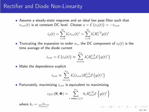
Rectifier and Diode Non-Linearity
• Assume a steady-state response and an ideal low pass filter such thatvout(t) is at constant DC level. Choose a = E vd(t) = −vout.
id(t) =∞∑
i=0
k′ivin(t)i =
∞∑
i=0
k′iRi/2s y(t)i
• Truncating the expansion to order no, the DC component of id(t) is thetime average of the diode current
iout = E id(t) ≈no∑
ieven
k′iRi/2antE
y(t)i
• Make the dependence explicit
iout ≈no∑
ieven
k′i(iout)Ri/2antE
y(t)i
• Fortunately, maximizing iout is equivalent to maximizing
zDC(S,Φ) =
no∑
i even,i≥2
kiRi/2antE
y(t)i
where ki =is
i!(nvt)i
26 / 84

Linear Model
Linear Model: Truncate to order 2
zDC = k2RantEy(t)2
=k22Rant
[N−1∑
n=0
|hnwn|2]
• max zDC = max Ey(t)2
= maxP rrf
• Tx strategy that maximizes P rrf is the same strategy that maximizes P rdc
• Maximizing e2 × e3 corresponds to maximizing e2 with constant e3, i.e.coupling between e2 and e3 ignored by assuming e3 constant
• Assume sufficiently low input RF power such that the higher-order termswould not contribute to zDC
27 / 84

Nonlinear Model
Nonlinear Model: Truncate to a higher-order term, e.g. order 4 (no = 4)
zDC = k2RantEy(t)2
︸ ︷︷ ︸
Linear term
+ k4R2antE
y(t)4
︸ ︷︷ ︸
Nonlinear term
• Non-linearity characterized through Ey(t)4
• Maximizing zDC or equivalently e2 × e3 does not lead to the same solutionas maximizing e2 only
• Assume M = 1 and no = 4
zDC(S,Φ) =k2
2Rant
[
N−1∑
n=0
s2nA
2n
]
+3k4
8R
2ant
∑
n0,n1,n2,n3n0+n1=n2+n3
[
3∏
j=0
snjAnj
]
cos(ψn0+ ψn1
− ψn2− ψn3
)
• Assuming is = 5µA, a diode ideality factor n = 1.05 and vt = 25.86mV ,typical values are given by k2 = 0.0034 and k4 = 0.3829.
28 / 84

Signal/Waveform Design
Design amplitudes and phases to maximize the DC output power subject toTx power constraint using the linear and nonlinear models
Assume CSI (frequency response hn,m) known to the Tx (CSIT)
Original problem: Maximize the DC output current iout
maxS,Φ
iout(S,Φ) = k′0 + k′2RantEy(t)2
+ k′4R
2antE
y(t)4
+ ...
subject to1
2‖S‖2F ≤ P
Equivalent problem: Maximize the quantity zDC
maxS,Φ
zDC(S,Φ) = k2RantEy(t)2
︸ ︷︷ ︸
Linear term
+ k4R2antE
y(t)4
+ ...
︸ ︷︷ ︸
Nonlinear terms
subject to1
2‖S‖2F ≤ P
29 / 84

Design based on Linear Model
Problem
maxwn
N−1∑
n=0
|hnwn|2 s.t.1
2
[N−1∑
n=0
‖wn‖2]
≤ P
Solution: matched (energy) beamformer on a single sinewave, namely the onecorresponding to the strongest channel n = argmaxi ‖hi‖2
w⋆n =
√2P h
Hn / ‖hn‖ , n = n,
0, n 6= n.
Adaptive Single Sinewave (ASS) strategy: allocate all power to a singlesinewave, the one corresponding to the strongest channel
• A single-sine waveform favoured over a multisine waveform
• Exploits frequency-diversity gain and spatial energy-beamforming gain
30 / 84

Design based on Nonlinear Model: A Toy Example
Assume N = 2, M = 1 and real frequency domain channel
zDC(s0, s1) = k2Rant/2(s20A
20 + s21A
21
)+ 3k4R
2ant/8
[(s20A
20 + s21A
21
)2+ 2s20s
21A
20A
21
]
Transmit power constraint s20 + s21 = 2P
Lagrangian optimization: 3 stationary points (2P, 0), (0, 2P ) and (s⋆20 , s⋆21 )
s02
s 12
0 1 2
x 10−4
0
0.5
1
1.5
2
2.5x 10
−4
2
4
6
8
10
12x 10
−5
0.5 0.75 1 1.25 1.50
0.2
0.4
0.6
0.8
1x 10
−4
A1
z DC
[A]
s02
s 12
0 1 2
x 10−4
0
0.5
1
1.5
2
2.5x 10
−4
5
10
15
x 10−5
s02
s 12
0 1 2
x 10−4
0
0.5
1
1.5
2
2.5x 10
−4
0.5
1
1.5
2x 10
−4
s1=0
s0=0
opt
A0=1 A
0=1, A
1=0.75
A0=1, A
1=1 A
0=1, A
1=1.15
31 / 84

Design based on Nonlinear Model: A Toy Example
Lagrangian optimization leads to 3 stationary points:
1 (2P, 0): Allocate all power to the first sinewave if A0 >> A1
2 (0, 2P ): Allocate all power to the second sinewave if A0 << A1
3 (s⋆20 , s⋆21 ): Allocate power to both sinewaves if A0 ≈ A1
The first two points correspond to the ASS strategy → ASS is in generalsuboptimal with the nonlinear model
Benefits of allocating power over multiple sinewaves for some channel states
RF experiments show the benefits of allocating power uniformly across multiplesinewaves
• Nonlinear model-based design backs up the experimental results
• Linear model and ASS cannot explain RF experiment results
General approach? for any order no, N , M?
32 / 84

Design based on Nonlinear Model: General Approach
Globally optimal phases in closed-form: φ⋆n,m = −ψn,m so as ψn,m = 0 ∀n,m.
zDC(S,Φ⋆) is a posynomial
• Monomial g : RN++ → R : g(x) = cxa11 xa22 . . . xaNN where c > 0 and ai ∈ R.
• Posynomial f(x) =∑Kk=1 gk(x), gk(x) = ckx
a1k1 x
a2k2 . . . x
aNkN , ck > 0.
Amplitudes: Non-convex Posynomial Maximization Problem
maxS
zDC(S,Φ⋆)
subject to1
2‖S‖2F ≤ P.
minS,t0
1/t0
subject to1
2‖S‖2F ≤ P,
t0/zDC(S,Φ⋆) ≤ 1.
Formulate as a Reversed Geometric Program and solve iteratively
• lower bound zDC(S,Φ⋆) by a monomial zDC(S), i.e. upper bound
1/zDC(S,Φ⋆) by the monomial 1/zDC(S)
• Form of successive convex approximation or inner approximation method
33 / 84

Design based on Nonlinear Model: General Approach
AM-GM inequality: Arithmetic M ≥ Geometric M (γk ≥ 0,∑Kk=1 γk = 1)
zDC(S,Φ⋆) =
K∑
k=1
gk(S,Φ⋆) ≥
K∏
k=1
(gk(S,Φ⋆)/γk)
γk = zDC(S)
Tightness of the upper bound heavily depends on the choice of γk
(Local) Optimal WPT Waveform
Problem 1: Standard GP
minS,t0
1/t0
s.t.1
2‖S‖2F ≤ P,
t0
K∏
k=1
(gk(S,Φ
⋆)
γk
)−γk
≤ 1,
Algorithm
1: Initialize: i← 0, Φ⋆, S, z(0)DC = 0
2: repeat3: i← i+ 1, S← S
4: γk ← gk(S,Φ⋆)/zDC(S,Φ
⋆), ∀k5: S← argmin Problem 16: z
(i)DC ← zDC(S,Φ
⋆)
7: until∣∣∣z
(i)DC − z
(i−1)DC
∣∣∣ < ǫ or i = imax
Convergence to a KKT point guaranteed, not a global optimum34 / 84
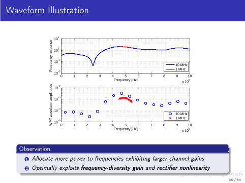
Waveform Illustration
0 1 2 3 4 5 6 7 8 9 10
x 106
10−2
10−1
100
101
Frequency [Hz]
Fre
quen
cy r
espo
nse
0 1 2 3 4 5 6 7 8 9 10
x 106
10−5
10−4
10−3
10−2
Frequency [Hz]
WP
T w
avef
orm
am
plitu
des
10 MHz1 MHz
10 MHz1 MHz
Observation
1 Allocate more power to frequencies exhibiting larger channel gains
2 Optimally exploits frequency-diversity gain and rectifier nonlinearity
35 / 84

Decoupling Space and Frequency Domains
Decoupling Space and Frequency Domains without impacting performance
1 Matched (energy) beamformer
wn = snhHn / ‖hn‖
Multi-antenna multi-sine WPT weight optimization converted into aneffective single antenna multi-sine WPT weight optimization
2 Optimize magnitude sn based on effective channel gain ‖hn‖ subject to∑N−1n=0 s
2n = 2P . Use Reversed GP.
Same performance as the joint space-frequency design but lowercomputational complexity
Exploits frequency-diversity gain, spatial energy-beamforming gain andrectifier nonlinearity
Decoupling only optimal in SU WPT
36 / 84

PAPR Constraints
PAPR on antenna m defined as
PAPRm =maxt |xm(t)|2E|xm(t)|2 =
maxt |xm(t)|212‖sm‖2
Waveform design subject to PAPR constraints
maxS,Φ
iout(S,Φ)
subject to1
2‖S‖2F ≤ P,
PAPRm ≤ η, ∀m.
PAPR constraints leads to signomials. Solved using Reversed GP as well.
Decoupling the space and frequency domains leads to a suboptimal designcompared to the joint space-frequency design in the presence of PAPRconstraints.
37 / 84

Scaling Laws (N >> 1,M = 1, no = 4)
Waveform Frequency-Flat (FF) Frequency-Selective (FS)
No CSIT
zDC,UP k2RantP + 2k4R2antP
2N k2RantP + 3k4R2antP
2
CSIT
zDC,ASS k2RantP + 3k4R2antP
2 k2RantP logN + 32k4R
2antP
2 log2N
zDC,UPMF k2RantP + 2k4R2antP
2N k2RantP + k4R2antP
2N
Observation
1 Linear increase with N in FF and FS channels.
2 CSIT not needed in FF channels but needed in FS channels.
3 linear model-based design (ASS) leads to significantly lower scaling lawsthan the non-linear model-based design for FF and FS channels.→ increase in logN vs N .
38 / 84

Scaling Laws (N >> 1,M >> 1, no = 4)
Large-Scale Multi-Sine Multi-Antenna WPT
zDCN,Mր≈ k2RantPM + k4R
2antP
2NM2
for both FF and FS channels
Easily achieved by matched energy beamforming and uniform power allocationfor N,M very large
The large dimension enables to significantly simplify the waveform design
Reminiscent of Massive MIMO in communication
39 / 84

Linear vs Non-linear Regime
The 2nd order term is G times larger than the 4th order term if
P rrf ≤k2k4
1
Rant
1
N
1
G
100
101
102
10−7
10−6
10−5
10−4
N
Prfr [W
]
2nd order term > 4th order term
2nd order term > 10 * 4th order term
2nd order term > 100 * 4th order term
4th order term > 2nd order term
40 / 84

Performance Evaluations
WiFi-like environment
• 5.18GHz, 36dBm Tx power, 2dBi Rx antenna gain, 58dB path loss, office.
• Average received power of about -20dBm.
• Frequency gap fixed as ∆w = 2π∆f with ∆f = B/N .
Metric: zDC = k2RantEy(t)2
+ k4R
2antE
y(t)4
• k2 = 0.0034, k4 = 0.3829, Rant = 50Ω.
41 / 84

Performance Evaluations
B=1MHz (left) and B=10MHz (right)
(1,1) (2,1) (4,1) (8,1) (16,1) (1,2) (2,2) (4,2) (8,2)0
1
2
3
4
5
6
7
8
9
Ave
rage
zD
C d
eliv
ered
to lo
ad [u
A],
B =
1M
Hz
non−adaptive UPadaptive MFadaptive SSadaptive OPT
(1,1) (2,1) (4,1) (8,1) (16,1) (32,1) (1,2) (2,2) (4,2) (8,2)0
2
4
6
8
10
12
Ave
rage
zD
C d
eliv
ered
to lo
ad [µ
A],
B =
10M
Hz
non−adaptive UPadaptive MFadaptive SSadaptive OPT
Observation
1 Nonlinear model-based design outperforms the linear model-based design
2 Nonlinearity non-negligible at low input power, e.g. -20dBm (10µW )
3 OPT waveforms jointly exploit beamforming gain, channelfrequency-selectivity and rectifier nonlinearity
4 ASS (optimal linear model-based design) worse than non-adaptive UP!
42 / 84

Performance Evaluations
Large-scale multisine waveforms - B=5MHz - M = 1
24 8 16 32 64 1280
5
10
15
20
25
Number of sinewaves N
Ave
rage
zD
C [µ
A]
non−adaptive UPadaptive SSadaptive UPMFadaptive MF
Observation
1 Significant loss of linear model-based waveform design for N ≥ 8
43 / 84

Performance Evaluations
Effect of Bandwidth B on zDC for N = 16 and M = 1.
1 2.5 5 7.5 100
1
2
3
4
5
6
7
8
Bandwidth [MHz]
Ave
rage
zD
C [µ
A]
non adaptive UPadaptive MFadaptive SSadaptive OPTadaptive MAX PAPRadaptive UPMF
Observation
1 Importance of non-uniform power allocation as Bandwidth increases
2 MAX PAPR waveform not a suitable approach!44 / 84

Performance Evaluations
zDC of OPT waveform versus transmit PAPR for N = 16 and M = 1.
4 5 6 7 8 9 10 11 12 13 14 1510
−1
100
101
PAPR [dB]
z DC [µ
A]
data − 1 MHzlinear reg. − 1MHzdata − 5 MHz linear reg. − 5MHzdata − 10 MHz linear reg. − 10 MHz
Observation
1 As bandwidth increases, correlation between DC current and PAPR reduces
2 Careful with the use of PAPR as a measure of waveform performance!45 / 84

Performance Evaluations
zDC versus transmit PAPR constraint for N = 8 and M = 1.
1 2 4 8 16 321
2
3
4
5
N
z DC [µ
A]
OPTUP
4 5 6 7 8 9 10 11 12
1.8
2
2.2
2.4
2.6
PAPR constraint η [dB]
z DC [µ
A]
1 2 3 4 5 6 7 810
−5
10−4
10−3
10−2
index of sinewave
Wav
efor
m a
mpl
itude
s
η=4dBη=6dBη=8dBη=10dBη=12dB
N=4 − No PAPR constraint
N=2 − No PAPR constraint
N=1
Observation
1 In frequency flat channel, UP close to optimal
2 As η decreases, less power on the side and more on the center frequencies46 / 84

Circuit Evaluations
Rectenna with a single diode and a L-matching network used for PSpiceevaluations with B = 10MHz.
• Designed for an input power of -20 dBm
• Good matching between the rectifier and the antenna and minimizeimpedance mismatch due to variations in frequency and input power level
• C1 and L1 optimized to match the antenna impedance to the averageinput impedance of the rectifier resulting from an input signal composedof 4 sinewaves and spread across B = 10 MHz
The output capacitor chosen as C2 = Cout = 100pF for B = 1MHz47 / 84

Circuit Evaluations
Matlab/CVX (left) and PSpice (right) - B=1MHz
(1,1) (2,1) (4,1) (8,1) (16,1) (1,2) (2,2) (4,2) (8,2)0
1
2
3
4
5
6
7
8
9
Ave
rage
zD
C d
eliv
ered
to lo
ad [u
A],
B =
1M
Hz
non−adaptive UPadaptive MFadaptive SSadaptive OPT
(1,1) (2,1) (4,1) (8,1) (16,1) (1,2) (2,2) (4,2) (8,2)0
0.5
1
1.5
2
2.5
3
3.5
4
4.5
5
DC
pow
er d
eliv
ered
to lo
ad,[u
W],
B =
1M
Hz
non−adaptive UPadaptive MFadaptive SSadaptive OPT
Observation
1 Good match between the nonlinear model and PSpice evaluations.
2 Nonlinear model-based design outperforms the linear model-based design.
3 Linear model does not characterize correctly the rectenna behavior.
4 Nonlinearity beneficial and exploitable in the low-power regime!
48 / 84

Circuit Evaluations
Matlab/CVX (left) and PSpice (right) - B=10MHz
(1,1) (2,1) (4,1) (8,1) (16,1) (32,1) (1,2) (2,2) (4,2) (8,2)0
2
4
6
8
10
12
Ave
rage
zD
C d
eliv
ered
to lo
ad [µ
A],
B =
10M
Hz
non−adaptive UPadaptive MFadaptive SSadaptive OPT
(1,1) (2,1) (4,1) (8,1) (16,1) (32,1) (1,2) (2,2) (4,2) (8,2)0
1
2
3
4
5
6
7
DC
pow
er d
eliv
ered
to lo
ad,[µ
W],
B =
10M
Hz
non−adaptive UPadaptive MFadaptive SSadaptive OPT
Observation
1 CSIT needed in frequency-selective channels.
2 Careful with PAPR metric!
3 OPT exploits BF gain + channel FS + rectifier nonlinearity.
49 / 84

Circuit Evaluations
Observation
1 Promising architecture: large-scale multisine multiantenna waveforms.
2 Sensors need 10 µW DC (see e.g. PsiKick’s Fully Integrated Wireless SoCsensors)
3 Think big: up to 2048 subcarriers in LTE! 100s antennas/Tx in 5G(Massive MIMO)!
50 / 84

Low-Complexity Signal Design
Reversed GP: a general approach applicable to any order no but exponentialcomplexity, not implementation friendly, difficult to tackle large-scale system
Low-Complexity Adaptive Multisine Waveform
• Idea: allocate more power to frequencies exhibiting larger channel gains• Scaled Matched Filter (SMF): sn = cAβn with c a constant• β = 1 leads to a matched filter-like behaviour, i.e. MRT• Aβn: amplify strong frequency components and attenuate weak ones
−5 −4 −3 −2 −1 0 1 2 3 4 510
−2
10−1
100
101
Frequency [MHz]
Fre
quen
cy r
espo
nse
−5 −4 −3 −2 −1 0 1 2 3 4 510
−6
10−5
10−4
10−3
10−2
Frequency [MHz]
WP
T w
avef
orm
am
plitu
des
OPTβ=1β=3
51 / 84

Circuit Evaluations
Single series, voltage doubler and diode bridge rectifiers
52 / 84

Average zDC and DC power with single series, voltagedoubler and diode bridge
1 2 4 8 16 320
1
2
3
4
5
6
7
8
9
Ave
rage
zdc
del
iver
ed to
load
, [µA
]
N
fixed (non−adaptive UP)adaptive MF (β=1)adaptive SMF, β=3adaptive SMF, β*adaptive OPT
1 2 4 8 16 320
1
2
3
4
5
6
7
N
DC
pow
er d
eliv
ered
to lo
ad, [
µW]
fixed (non−adaptive UP)adaptive MF (β=1)adaptive SMF, β=3adaptive SMF, β*adaptive OPT
1 2 4 8 16 320
1
2
3
4
5
6
N
DC
pow
er d
eliv
ered
to lo
ad, [
µW]
fixed (non−adaptive UP)adaptive MF (β=1)adaptive SMF, β=3adaptive SMF, β*adaptive OPT
1 2 4 8 16 320
0.5
1
1.5
2
2.5
3
3.5
4
4.5
N
DC
pow
er d
eliv
ered
to lo
ad, [
µW]
fixed (non−adaptive UP)adaptive MF (β=1)adaptive SMF, β=3adaptive SMF, β*adaptive OPT
Observation
1 Waveform design holds for single and multiple-diode rectennas
2 SMF very close to OPT despite much lower design complexity
3 At low input power, single series rectifier preferred53 / 84

Large-Scale WPT Architecture
Computationally efficient optimization framework:
• Reformulate the optimization problem by expressing the RF signal modelin a compact form using a real-valued function of complex vector variables
• Limited to 4th order (no = 4)
Wireless channel h = [hT1 , . . . ,hTN ]T ∈ C
MN×1
Waveform precoder s = [sT1 , . . . , sTN ]T ∈ C
MN×1
Rectenna output DC voltage (zDC = vout is/(nvt))
vout = β2∑Nn=1s
Hn h
∗nh
Tn sn +
32β4
∑n1,n2,n3,n4
n1−n3=−(n2−n4)sHn3h∗n3hTn1sn1 ·s
Hn4h∗n4hTn2sn2
Computational efficiency: SU WPT vs. Reversed GP
Algorithms Average vout [V]Average elapsed
time [s]
Average
convergence time
SU WPT 9.532× 10⁻² 1.752× 10⁻³ 4.18 iterations
Reversed GP 8.417× 10⁻² 99.04 17.16 iterations
• M = 1, N = 8, P = 3.98107W and a distance of 10m
• Stopping criteria: (v(l)out − v(l−1)
out )/v(l)out ≤ 10−3
54 / 84

Large-Scale WPT Architecture
Average vout achieved by SU WPT (left) and ASS (right) vs. distance(P = 0.5W)
• SU WPT: computationally efficient optimal nonlinear model-basedwaveform design
• ASS: optimal linear model-based waveform design
10 12 14 16 18 2010
−2
10−1
100
Distance [m]
Ave
rage
vou
t [V]
SU WPTReference
M=32,N=32
M=32,N=16
M=16,N=16
M=16,N=8
M=8,N=8
10 12 14 16 18 2010
−2
10−1
100
Distance [m]A
vera
ge v
out [V
]
ASS M=32 N=32ASS M=32 N=16ASS M=16 N=16ASS M=16 N=8ASS M=8 N=8Reference
Observation
1 Significant benefits of the architecture to boost the end to end power
transfer efficiency and the transmission range
55 / 84

Unmodulated vs Modulated Signals
Multisine waveform is deterministic while modulated waveform exhibitsrandomness due to information symbols
Randomness has an impact on the amount of harvested energy and needs to becaptured in the rectenna model
Proposed model for the DC current with a multi-carrier modulated waveform
yI(t) = ℜN−1∑
n=0
hnwI,nxnej2πfnt
,
zDC =
no∑
i even,i≥2
kiRi/2antExn
A
yI(t)i
,
by averaging out over the distribution of the input symbols xn
56 / 84

Scaling Laws - Single-Carrier
Waveform Frequency-Flat (FF)
Modulated (CSCG)
zDC k2RantP + 6k4R2antP
2
Unmodulated (CW)
zDC k2RantP + 3k4R2antP
2
Observation
1 From 2nd order term: Modulated and Unmodulated waveforms are equallysuitable.
2 From 4th order term: Modulated better than Unmodulated.
3 Gain of modulation comes from large fourth order moment with CSCGinputs.
57 / 84

Scaling Laws - Multi-Carrier
Waveform Frequency-Flat (FF) Frequency-Selective (FS)
Modulated
zDC k2RantP + 6k4R2antP
2 k2RantP logN + 3k4R2antP
2 log2N
Unmodulated
zDC k2RantP + 2k4R2antP
2N k2RantP + k4R2antP
2N
Observation
1 From 2nd order term: Modulated and Unmodulated waveforms are equallysuitable.
2 From 4th order term: Unmodulated better than Modulated.
3 Loss in scaling law is inherently due to the randomness of informationsymbols across subbands.
58 / 84

Unmodulated vs Modulated Signals
DC power vs N (left) and CCDF of PAPR with OFDM vs N (right)
0 2 4 6 81
1.5
2
2.5
3
3.5x 10
−6
log2(N)
PD
C [W
]
0 2 4 6 8 10 12 1410
−2
10−1
100
PAPR [dB]C
CD
F
MultisineOFDM with Gaussian inputs
N=1N=2N=4N=8N=16
Observation
1 Random fluctuation of OFDM waveform vs periodic behavior of multisine
waveform (more suitable to turn on and off the rectifier periodically)
2 DC power of OFDM insensitive to N despite PAPR increase with N
3 Careful again with PAPR metric!59 / 84

Modulated Signals
Energy Modulation for WPT? Complex Gaussian, Real Gaussian, somethingelse?
Flash signaling distribution
pr(r) =
1− 1l2, r = 0,
1l2, r = l,
with l ≥ 1.
Low probability of high amplitude signal
Boost the fourth order term in the Taylor expansion: Er4= l2
60 / 84

Multi-User WPT Signal Design
Multi-User WPT: WPT to K single-antenna users/rectennas
• Rectennas belong to a single user (i.e. point-to-point MIMO WPT)
• Rectennas spread across multiple users
Trade-off: zDC,q in general depends on zDC,p, p 6= q
Energy Region ZDC : set of all rectenna harvested energy (zDC,1, . . . , zDC,K)that are simultaneously achievable
Boundary of ZDC : weighted sum of zDC,k with weights vk, k = 1, . . . ,K
maxS,Φ
ZDC(S,Φ) =K∑
k=1
vkzDC,k(S,Φ) s.t.1
2‖S‖2F ≤ P
61 / 84

Energy region
Energy region: Achievable vout region, with M = 20 and N = 10
1 2 3 4 5 6 7
2
4
6
8
vou
t of u
ser
1 [m
V]
vout
of user 2 [mV]
WSumTDMA 1CHE WSumTDMA 2
Observation
1 Achievable energy region with WSum larger than that of TDMA
Design extendable to max-min problem: maxmink∈1,...,K zDC,k62 / 84

Multi-User WPT: Network Architecture
J distributed ETs simultaneously serve K ERs each having multiple antennas
Three main networking architectures (with complexity from high to low):
CoMP(Coordinated Multi-Point) WPT
• All ETs jointly design energy signals to the K ERs based on global CSI
• Only requires exchange of CSI and waveform parameters among ETs, asopposed to message exchange in CoMP communications
Locally-coordinated WPT
• Each ER is served by a subset of ETs
• ET-oriented association:group the ETs into clusters, with each cluster ETscooperatively serving a subset of ERs
• ER-oriented association:each ER is freely associated with a subset of ETs
Single-ET WPT: Each ER served by exactly one ET63 / 84

Co-located Antenna System vs Distributed Antenna System
Simulation assumptions:
• A WPT system that serves a square area of 30m x 30m with co-locatedversus distributed antennas
• Co-located antennas: a single ET with 9-element uniform linear array(ULA) at the center of the serving area
• Distributed antennas: 9 ETs each with single antenna equally spaced inthe area
• Two single-antenna ERs at (15m, 5m) and (18.88m, 29.49m), which are10m and 15m away from the area center, respectively
• Total transmit power of the system is 2W
• Maximize the minimum (max-min) harvested power by the two ERs
64 / 84

Co-located Antenna System vs Distributed Antenna System
X= 15Y= 5Level= 42.4145
x [m]
y [m
]
X= 18.9Y= 29.5Level= 42.4475
0 5 10 15 20 25 300
5
10
15
20
25
30[uW]
0
20
40
60
80
100
120
140
160
180
200
X= 15Y= 5Level= 45.3642
x [m]
y [m
]
X= 18.9Y= 29.5Level= 46.8895
0 5 10 15 20 25 300
5
10
15
20
25
30[uW]
0
20
40
60
80
100
120
140
160
180
200
Observation
1 Power beamed towards the ERs in co-located antenna system
2 More even spatial power distribution for distributed antenna system
65 / 84

Channel Acquisition for WPT
Waveform/beamforming requires Channel State Information (CSI) at Tx
Unique considerations for CSI acquisition in WPT in contrast to conventionalwireless communication
• CSI at (energy) receiver: not required for WPT
• Net energy maximization: to balance the energy overhead for CSIacquisition and the energy harvested with CSI-based energy beamforming
• Hardware constraint: no/low signal processing capability for low-cost ERs
Candidate solutions depending on the antenna architecture at Rx
• Forward-link training with CSI feedback
• Reverse-link training via channel reciprocity
• Power probing with limited energy feedback
66 / 84

Channel Acquisition Schemes for WPT
67 / 84

Multi-Antenna Multi-Sine WPT with Limited Feedback
ET: M Tx antennas and N frequencies; ER: K rectennas
Waveform Selection-based WPT
• Waveform precoders: a predesigned Np-codeword codebook
• ER feedback: n⋆p = argmaxnp∈1,...,Np ZDC([S]np)
• log2Np feedback bits and Np energy signals transmitted in the WS phase
68 / 84

Multi-Antenna Multi-Sine WPT with Limited Feedback
Waveform Refinement-based WPT
• Waveform precoders: a predesigned tree-structured codebook
• ER: fb = 1, for ZDC,q([Sl,ns
]
1) > ZDC,q(
[Sl,ns
]
2); otherwise, fb = 0.
• log2Np feedback bits and 2 log2Np energy signals sent in WR phase69 / 84

Multi-Antenna Multi-Sine WPT with Limited Feedback
Average vout in the WPT phase as a function of N , with M = 1 and K = 1(P = 36dBm)
• In the WS-based WPT, the codebook size Np = 2N .
• In the WR-based WPT, the TS codebook has L = log2 2N levels.
N = 8 N = 16 N = 320
0.05
0.1
0.15
0.2
0.25
Ave
rage
vou
t [V]
SU WPTWS−based WPTWR−based WPTASSUPIso. trans.
Observation
1 Proposed waveform strategies, based on limited feedback, outperform thelinear model-based waveform design relying on perfect CSIT
70 / 84

Prototyping and Experimentation of Closed-Loop WPT
Demonstrate the first prototype of a closed-loop WPT system with adaptivewaveform optimization based on CSI acquisition
Establish an experimental environment for closed-loop WPT with waveformoptimization
• Design optimized multi-sine RF Tx
• Implement CSI acquisition/channel estimator
• Design efficient rectenna
Verify advantages of CSI-based optimized signal for WPT
71 / 84

Actual Prototype Architecture
Transmitter
Receiver Part. A
LO
2.4 GHz
Power Amp
Signal
generation
OFDM Modulator
for Channel Estimation
Signal
Optimization
푓(푥) 푑
푑푑푓(푑)휋
푓(푑)
풙+풚
푎+푏
휱
푺
Pilot IFFT
Energy Harvester
OFDM Demodulator
for Channel Estimation
FFT Channel
Estimation
RF Switch
or Power splitter
PXI equipment
Receiver Part. B
External Power Amp
Tx Antenna
Rx Antenna
Coaxial Cable
• The system operates in 2.4 GHz ISM band
• Software Defined Radio (SDR) used for transmitter and channel estimator.NI FlexRIO (PXI-7966R) and transceiver module (NI 5791R)
• Channel estimation and waveform design implemented in LabVIEW
72 / 84

Actual Prototype Architecture
Equipment and peripherals
Rectenna (Receiver Part. B)
External Power Amp
Power Supply for external amp
RF Power Meter
Multimeter
PXI equipment
Rx Antenna and Power splitter to Tx Antenna
73 / 84

Actual Prototype Architecture
Channel estimation: pilot based channel estimation technique
Parameter Value
Bandwidth 20 MHz
Number of Subcarriers 256
Frequency Spacing 78.125 KHz
Pilot type Block type pilot
Number of symbols for channel estimation 20 symbols (320 µs)
Method of Channel Estimation Least-square
Waveform design: Scaled Matched Filter (SMF) because of low complexityand processing time
• N uniformly spaced sinewaves in 10MHz bandwidth, Tx Power of 35dBm
74 / 84

Actual Prototype Architecture
Latest Rectenna Design
12 kohm
D1SMS7630-079LF
D2SMS7630-079LF
0.3 nH
1.5 pF 0.33 pF 2.7 nF
2.7 nF
1.6 mm FR4 substrate
75 / 84

Latest Measurement Results
Received DC power as a function of N with 10 MHz bandwidth in NLoS
1-Tone 2-Tone 4-Tone 8-Tone 16-Tone
Number of Sinewaves N
0
0.5
1
1.5
2
2.5
3
3.5
non-adaptive UPadaptive MAX PAPRadaptive SS
Observation
1 Measurements confirm theory: gains very promising
76 / 84

Conclusions and Future Challenges
1 WPT: Introduction and Applications
2 RF, Signal and System Design for WPT
3 Conclusions and Future Challenges
77 / 84

Conclusions
Communications and signals for WIPT systems (WPT, SWIPT, WPCN,WPBN)
• Lay the foundations and tackle the challenges of the envisioned network
• Establish a mobile power link and system-level design inspired bycommunication theoretic ideas
• Develop a signal theory for transmission over the nonlinear wireless powerchannel and the linear wireless communication channel
• Identify the fundamental tradeoff between conveying information andpower wirelessly
Non-linearity is a fundamental property of the rectifier and cannot be ignored
• The wireless power channel is non-linear
• This contrasts with the wireless communication channel ... commonlyassumed linear
• Importance of accounting for the non-linearity of the rectenna in anydesign involving wireless power: WPT, SWIPT, WPCN, WPBN
Need for bridging RF and comms/signal processing78 / 84

WPT Extensions and Future Work
Energy Harvester Modeling and impact on signal design: Non-linearity ofrectifier (diode), Non-linearity due to impedance mismatch, Non-linearity dueto saturation, Harmonics
Optimal transmit signal for WPT unknown: optimal input distribution,deterministic or modulated waveforms, role of modulation, energy outageminimization
Role played by CSI in WPT remains largely unknown: channel acquisition infrequency-selective and/or multi-user channels, impact of CSIT on signaldesign, distributed channel training and waveform
Low-complexity algorithm
Massive MIMO and mmWave WPT
safety and health: importance of CSI acquisition, distributed antenna systemand signal design
Coexisting with wireless communication and interference management
Higher layer (MAC, Network, etc.) design issues in WPT
Hardware development and applications79 / 84

Future Work Directions
• Wireless energy harvesting (WEH) and wireless power transfer (WPT)• Simultaneous wireless information and power transfer (SWIPT)• Wirelessly powered communication networks (WPCNs)• Wirelessly powered backscatter communication (WPBC)• Analytical models of energy harvesters for signal, system and architecture design• Fundamental limits of signal design for WPT, SWIPT, WPCN and WPBC• Communications and signal design for WPT, SWIPT, WPCN and WPBC• Waveform and beamforming design for WPT, SWIPT, WPCN and WPBC• Channel estimation, feedback and acquisition for WPT, SWIPT, WPCN and WPBC• WEH, WPT, SWIPT, WPCN and WPBC in pt-to-pt, BC, IC and relay channels• Multi-node coordination/cooperation for WPT, SWIPT, WPCN and WPBC• Network architecture and protocols for WEH, WPT, SWIPT, WPCN and WPBC• Wireless charging control, energy management, resource allocation and scheduling strategies
for WPT, SWIPT, WPCN and WPBC• Large-scale multi-antenna/massive MIMO in WPT, SWIPT, WPCN and WPBC• WEH, WPT, SWIPT, WPCN and WPBC at mmWave frequencies• Safety, security and economic issues in WPT, SWIPT, WPCN and WPBC• Spectrum sharing an interference management for coexisting WPT and WIT systems• Prototyping and experimentation of WEH, WPT, SWIPT, WPCN and WPBC• Applications of WEH, WPT, SWIPT, WPCN and WPBC in wireless sensor networks
(WSNs), machine-to-machine (M2M), device-to-device (D2D), Internet-of-Things (IoT),WiFi, cellular networks and 5G
80 / 84

References I
WPT introduction and overview in RF literatureZ. Popovic, “Cut the cord: Low-power far-field wireless powering,” IEEE Microwave Mag., vol.
14, no. 2, pp. 55–62, Mar. 2013.
A. Boaventura, A. Collado, N. B. Carvalho, and A. Georgiadis, “Optimum Behavior: Wireless
Power Transmission System Design through Behavioral Models and Efficient Synthesis
Techniques,” IEEE Microw. Mag., vol. 14, no. 2, pp. 26-35, Mar./Apr. 2013.
H.J. Visser, R.J.M. Vullers, “RF Energy Harvesting and Transport for Wireless Sensor Network
Applications: Principles and Requirements,” Proceedings of the IEEE | Vol. 101, No. 6, June
2013.
Z. Popovic, E. A. Falkenstein, D. Costinett, and R. Zane, “Low-power far-field wireless
powering for wireless sensors,” Proc. IEEE, vol. 101, no. 6, pp. 1397–1409, Jun. 2013.
S. Hemour and K. Wu, “Radio-Frequency Rectifier for Electromagnetic Energy Harvesting:
Development Path and Future Outlook,” Proceedings of the IEEE, Vol. 102, No. 11,
November 2014.
A. Costanzo and D. Masotti, “Smart solutions in smart spaces: Getting the most from far-field
wireless power transfer,” IEEE Microw. Mag., vol. 17, no. 5, pp. 30–45, May 2016.
B. Clerckx, A. Costanzo, A. Georgiadis, and N. B. Carvalho, “Towards the 1G of Mobile Power
Network: RF, Signal and System Designs to Make Smart Objects Autonomous” submitted to
IEEE Microw. Mag., arXiv:1712.06088.
81 / 84

References II
Communications and Signals Design for WPTY. Zeng, B. Clerckx and R. Zhang, “Communications and Signals Design for Wireless Power
Transmission,” IEEE Trans. on Comm, invited paper, Vol 65, No 5, pp 2264 - 2290, May 2017.
Fundamentals of WPT waveform designsB. Clerckx and E. Bayguzina, “Waveform Design for Wireless Power Transfer,” IEEE Trans on
Sig Proc, Vol. 64, No. 23, pp. 6313-6328, Dec 2016.
Low-complexity design of WPT waveformB. Clerckx and E. Bayguzina, “A Low-Complexity Multisine Waveform Design for Wireless
Power Transfer,” IEEE Ant. and Wireless Propag. Letters, vol 16, pp 2207 – 2210, 2017.
Large scale design for WPT waveformsY. Huang and B. Clerckx, “Large-Scale Multi-Antenna Multi-Sine Wireless Power Transfer,”
IEEE Trans. on Sig Proc., vol. 65, no. 21, pp 5812-5827, Nov 2017.
CSI feedback/acquisition in WPTY. Huang and B. Clerckx, “Waveform Design for Wireless Power Transfer with Limited
Feedback,” IEEE Trans. on Wireless Commun., vol. 17, no. 1, pp 415-429, Jan. 2018.
Prototyping and Experimentation of WPTJ. Kim, B. Clerckx, and P.D. Mitcheson, “Prototyping and Experimentation of a Closed-Loop
Wireless Power Transmission with Channel Acquisition and Waveform Optimization,” IEEE
WPTC 2017.
82 / 84

References III
Fundamentals of Wireless Information and Power TransferB. Clerckx, R. Zhang, R. Schober, D. W. K. Ng, D. I. Kim, and H. V. Poor, “Fundamentals of
Wireless Information and Power Transfer: From RF Energy Harvester Models to Signal and
System Designs,” arXiv:1803.07123
Signal Design for Wireless Information and Power TransferB. Clerckx, “Wireless Information and Power Transfer: Nonlinearity, Waveform Design and
Rate-Energy Tradeoff,” IEEE Trans. on Sig. Proc., vol 66, no 4, pp 847-862, Feb. 2018.
Fundamental limits of Wireless Information and Power TransferM. Varasteh, B. Rassouli and B. Clerckx, “Wireless Information and Power Transfer over an
AWGN channel: Nonlinearity and Asymmetric Gaussian Signaling,” IEEE ITW 2017.
M. Varasteh, B. Rassouli and B. Clerckx, “On Capacity-Achieving Distributions Over Complex
AWGN Channels Under Nonlinear Power Constraints and their Applications to SWIPT,”
arXiv:1712.01226
83 / 84

References IV
This work has been partially supported by the EPSRC of the UK under grantsEP/M008193/1, EP/P003885/1.
84 / 84