fan48685 - fixed-output synchronous tinyboost regulator
TRANSCRIPT
© Semiconductor Components Industries, LLC, 2018
July, 2018 − Rev. 01 Publication Order Number:
FAN48685/D
FAN48685
Fixed-Output SynchronousTinyBoost� Regulator
DescriptionThe FAN48685 is a low−power boost regulator designed to provide
a minimum voltage−regulated rail from a standard single−cell Li−Ionbattery and advanced battery chemistries. Even below the minimumsystem battery voltage, the device maintains the output voltageregulation for an output load current of 800 mA. The combination ofbuilt−in power transistors, synchronous rectification, and low supplycurrent suit the FAN48685 for battery−powered applications.
The FAN48685 is available in a 9−bump, 0.4 mm pitch,Wafer−Level Chip−Scale Package (WLCSP).
Features
• Input Voltage Range: 2.5 V to 5.5 V
• 800 mA Max. Load Capability
• Forced Pass−Through Mode
• Three Output Voltage Programmability (3.6 V / 5.0 V / 5.45 V) viaMODE Pins
• 9−Bump, 0.4 mm Pitch WLCSP
• Four External Components: 0603 Inductor, 0402 Case Size Input,0402 2 x Output Capacitors
• This is a Pb−Free Device
Applications
• NFC Module Power
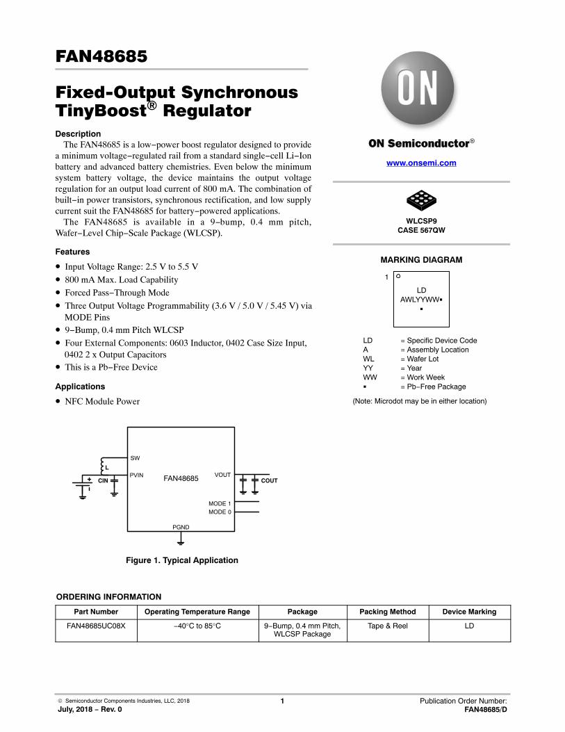
Figure 1. Typical Application
FAN48685
SW
PVIN VOUT
MODE 0
PGND
MODE 1
L
CIN COUT
ORDERING INFORMATION
Part Number Operating Temperature Range Package Packing Method Device Marking
FAN48685UC08X −40°C to 85°C 9−Bump, 0.4 mm Pitch,WLCSP Package
Tape & Reel LD
www.onsemi.com
WLCSP9CASE 567QW
MARKING DIAGRAM
(Note: Microdot may be in either location)
LDAWLYYWW�
�
1
LD = Specific Device CodeA = Assembly LocationWL = Wafer LotYY = YearWW = Work Week� = Pb−Free Package
FAN48685
www.onsemi.com2
Recommended External Components
Table 1. RECOMMENDED COMPONENTS
Component Description Vendor Parameter Typical Value Unit
L 470 nH 0603(1.6 mm x 0.8 mm x 0.65 mm max)
DFE1608CK−R47MMurata
L 0.47 �H
DCR 70 m�
ISAT 3.0 A
COUT 2 x 22 �F, 6.3 V, X5R, 0402 (1.0 mm x 0.5 mm)
GRM155R60J226ME11Murata
C 44 �F
CIN 10 �F, 6.3 V, X5R, 0402 (1.0 mm x 0.5 mm)
C1005X5R0J106M050BCTDK
C 10 �F
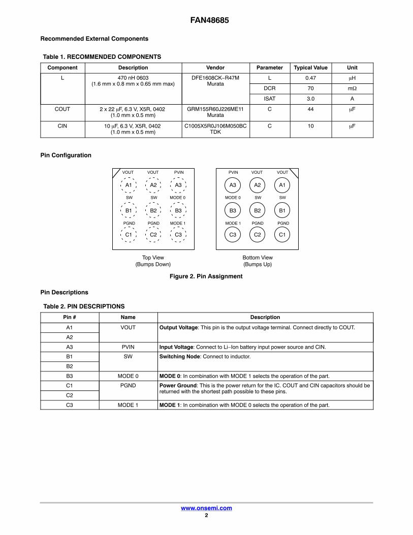
Pin Configuration
Figure 2. Pin Assignment
Top View(Bumps Down)
A1
VOUT
A2
VOUT
A3
PVIN
B1
SW
B2
SW
B3
MODE 0
C1
PGND
C2
PGND
C3
MODE 1
A3
VOUT
A2
VOUT
A1
PVIN
B3
SW
B2
SW
B1
MODE 0
C3
PGND
C2
PGND
C1
MODE 1
Bottom View(Bumps Up)
Pin Descriptions
Table 2. PIN DESCRIPTIONS
Pin # Name Description
A1 VOUT Output Voltage: This pin is the output voltage terminal. Connect directly to COUT.
A2
A3 PVIN Input Voltage: Connect to Li−Ion battery input power source and CIN.
B1 SW Switching Node: Connect to inductor.
B2
B3 MODE 0 MODE 0: In combination with MODE 1 selects the operation of the part.
C1 PGND Power Ground: This is the power return for the IC. COUT and CIN capacitors should bereturned with the shortest path possible to these pins.
C2
C3 MODE 1 MODE 1: In combination with MODE 0 selects the operation of the part.
FAN48685
www.onsemi.com3
Table 3. ABSOLUTE MAXIMUM RATINGS
Symbol Parameter Min Max Unit
PVIN Voltage on PVIN Pin −0.3 6.5 V
VOUT Voltage on VOUT Pin −0.3 6.5(1) V
VSW SW Node −0.3 6.5(1) V
VCTRL MODE 0, MODE 1 −0.3 6.5(1) V
ESD Electrostatic Discharge Protection Level Human Body Model, ANSI/ESDA/JEDEC JS−001−2012
2.0 kV
Charged Device Model, JESD22−C101 1.0
TJ Junction Temperature(2) −40 150 °C
TSTG Storage Temperature −65 150 °C
TL Lead Soldering Temperature, 10 Seconds 260 °C
Stresses exceeding those listed in the Maximum Ratings table may damage the device. If any of these limits are exceeded, device functionalityshould not be assumed, damage may occur and reliability may be affected.1. Lesser of 6.5 V or PVIN + 0.3 V.2. Please refer to Thermal Shutdown Protection in the Application information.
Table 4. RECOMMENDED OPERATING CONDITIONS
Symbol Parameter Min Typ Max Unit
PVIN Supply Voltage Range 2.5 5.5 V
L Inductor 0.470 0.611 �H
CIN Input Capacitance 10 �F
COUT Output Capacitance 5 (3) 2 x 22 �F
IOUT Maximum Output Current 800 mA
TA Ambient Temperature −40 85 °C
TJ Junction Temperature −40 125 °C
Functional operation above the stresses listed in the Recommended Operating Ranges is not implied. Extended exposure to stresses beyondthe Recommended Operating Ranges limits may affect device reliability.3. The minimum effective capacitance at the output for stability is 5 uF which includes the voltage derated affect with 5.45 V DC applied.
Table 5. THERMAL PROPERTIES
Symbol Parameter Typical Unit
�JA Junction−to−Ambient Thermal Resistance 50 °C/W
NOTE: Junction−to−ambient thermal resistance is a function of application and board layout. This data is measured with four−layer 2s2pboards with vias in accordance to JEDEC standard JESD51. Special attention must be paid not to exceed junction temperature,TJ(max), at a given ambient temperature, TA.
FAN48685
www.onsemi.com4
Table 6. ELECTRICAL CHARACTERISTICS (Notes 4, 5)Minimum and maximum values are at PVIN = 2.5 V to VOUT – 200 mV at TA = −40°C to +85°C, while typical values are at TA = 25°C andPVIN = 3.8 V, VOUT = 5 V otherwise noted.
Symbol Parameter Conditions Min Typ Max Unit
Power Supplies
IQ_PT IQ When part is in ForcedPass−Through
No Load 3 10 �A
VUVLO_RISE Under−Voltage Lockout PVIN Rising 2.10 2.15 2.24 V
VUVLO_FALL PVIN Falling 2.00 2.05 2.13 V
Output Accuracy
VO_ACC Regulated Output Voltage PVIN = 2.5 V, MODE[1:0] = 10,No Load, PWM Mode, TA = −10°C to +50°C
3.537 3.600 3.663 V
PVIN = 2.5 V, MODE[1:0] = 10,No Load, PWM Mode
3.510 3.600 3.690
PVIN = 3.8 V, MODE[1:0] = 01,No Load, PWM Mode, TA = −10°C to +50°C
4.913 5.000 5.088
PVIN = 3.8 V, MODE[1:0] = 01,No Load, PWM Mode
4.875 5.000 5.125
PVIN = 3.8 V, MODE[1:0] = 11,No Load, PWM Mode, TA = −10°C to +50°C
5.355 5.450 5.545
PVIN = 3.8 V, MODE[1:0] = 11,No Load, PWM Mode
5.314 5.450 5.586
Regulator
FSW Switching Frequency No Load, PVIN = 3.8 V 2.25 2.50 2.75 MHz
ISWLIM IL peak Current Limit PVIN = 2.5 V, Open Loop (Note 6) 2.88 3.63 4.46 A
LIN Soft−Start Input Linear Current Limit
90 200 mA
I/O Levels
VIL Low−Level Input Voltage 0.4 V
VIH High−Level Input Voltage 1.2 PVIN V
Product parametric performance is indicated in the Electrical Characteristics for the listed test conditions, unless otherwise noted. Productperformance may not be indicated by the Electrical Characteristics if operated under different conditions.4. Min and Max limits are specified by design, test and/or statistical analysis.5. Refer to Typical Characteristics waveforms/graphs for closed loop data and variation with input supply and temperature. Electrical
specifications reflect open loop steady state data.6. Current Limit specifications is tested open loop, for typical close loop current limit data, refer to typical performance characteristics

FAN48685
www.onsemi.com5
Table 7. SYSTEM SPECIFICATIONS (Note 7)
The following system specifications are guaranteed by designed and are not performed in production testing. Recommended operatingconditions, unless otherwise noted, PVIN = 2.5 V to VOUT – 200 mV, TA = 40°C to 85°C, VOUT = 5.45 V otherwise noted. Typical val-ues are given PVIN = 3.8 V and TA = 25°C. System Specifications area based on circuit per Figure 1. L = 0.47 �H (0603 DFE1608CK−R47M 70 m�/ 3.0 A) CIN = 10 uF (0402 C1005X5R0J106M050BC TDK) COUT = 2 x 22 uF (0402 GRM155R60J226ME11 MURATA.)
Symbol Parameter Conditions Min Typ Max Unit
Efficiency
� Efficiency VOUT = 5.45 V, IOUT = 100 mA 86 %
VOUT = 5.45 V, IOUT = 300 mA 92
VOUT = 5.45 V, IOUT = 500 mA 93
IOUT MAX
IOUT IOUT Max. 800 mA
VOUT Regulation
LOADREG Load Regulation 200 mA < IOUT < 600 mA, VOUT = 5.45 V −5 mV/A
LINEREG Line Regulation 3.0 V < PVIN < 4.2 V , IOUT = 550 mA, VOUT = 5.45 V
2 mV/V
Output Ripple
VRIPPLE Output Ripple IOUT = 550 mA, VOUT = 5.45 V, PVIN = 3.8 V 15 30 mV
IOUT = 450 mA, VOUT = 3.6 V, PVIN = 3.0 V 15 30
VOUT Transitions
TSETTLE VOUT Change MODE[1:0] 00 > 01 to 95% of VOUT, VOUT = Forced Pass−Through Mode > 5 V,IOUT = 1 mA
150 200 �s
MODE[1:0] 00 > 10 to 95% of VOUT, VOUT = Forced Pass−Through Mode > 3.6 V,IOUT = 1 mA, PVIN = 2.5 V to VOUT – 200 mV
100 200
ISS Soft−Start MODE[1:0] = 00, VOUT = PVIN (Start up intoForced Pass−Through Mode)
1.5 ms
Noise
en_bw Output Noise Voltage(Integrated)
VOUT = 5 V, IOUT = 550 mA, Freq = 0 Hz to 200 kHz
26 750 �V
VOUT = 5 V, IOUT = 550 mA, Freq = 50 kHz to 2 MHz
140 500
VOUT = 5 V and 3.6 V, IOUT = 550 mA, Freq = 13.5 MHz ± 200 kHz
70 300
Transients
VTRRP Load Transient IOUT = 10 mA ↔ 400 mA, TR = TF = 1 �s,VOUT = 5.45 V
±75 mV
VTRRP Load Transient PVIN = 3.0 V ↔ 3.5 V, TR = TF = 10 �s, IOUT = 550 mA, VOUT = 5.45 V
±75 mV
7. System Specifications are tested closed loop while using the recommended external components as listed on Table 1.
FAN48685
www.onsemi.com6
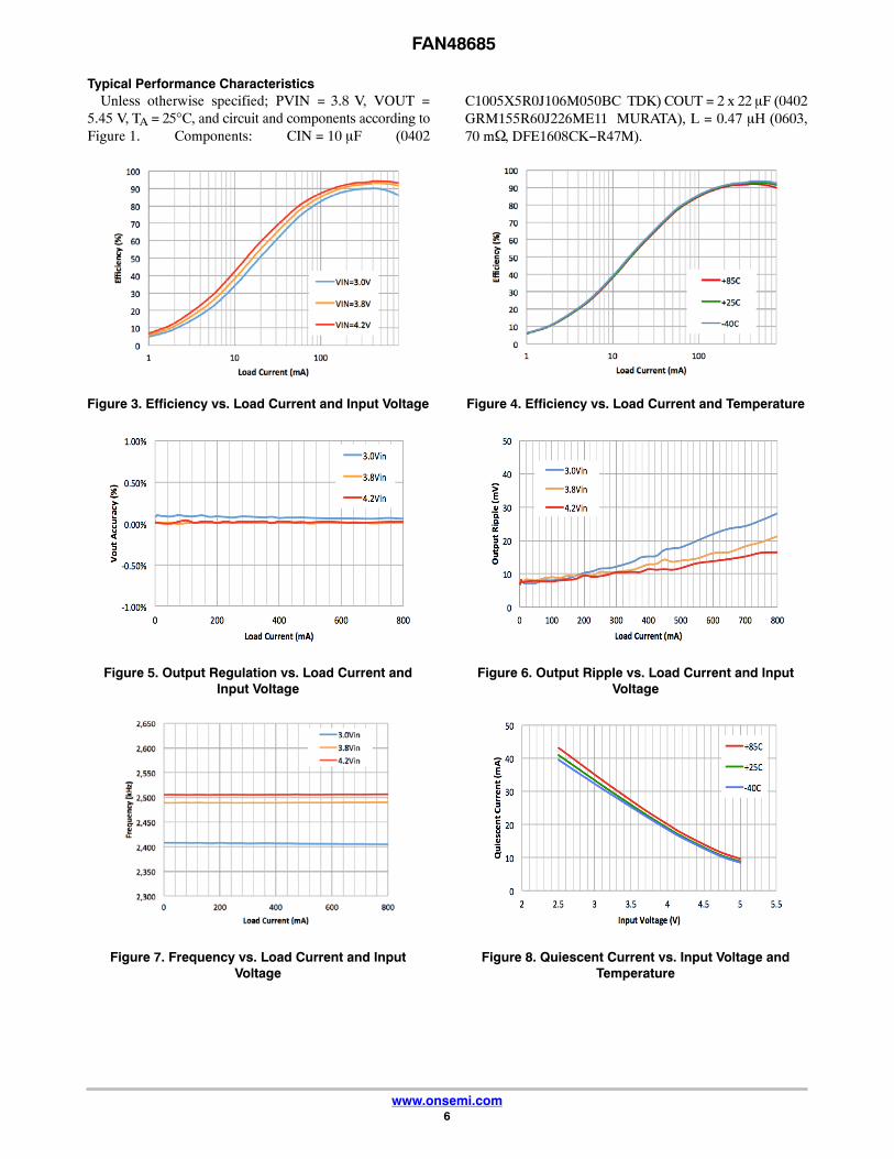
Typical Performance CharacteristicsUnless otherwise specified; PVIN = 3.8 V, VOUT =
5.45 V, TA = 25°C, and circuit and components according toFigure 1. Components: CIN = 10 �F (0402
C1005X5R0J106M050BC TDK) COUT = 2 x 22 �F (0402GRM155R60J226ME11 MURATA), L = 0.47 �H (0603,70 m�, DFE1608CK−R47M).
Figure 3. Efficiency vs. Load Current and Input Voltage Figure 4. Efficiency vs. Load Current and Temperature
Figure 5. Output Regulation vs. Load Current andInput Voltage
Figure 6. Output Ripple vs. Load Current and InputVoltage
Figure 7. Frequency vs. Load Current and InputVoltage
Figure 8. Quiescent Current vs. Input Voltage andTemperature
FAN48685
www.onsemi.com7
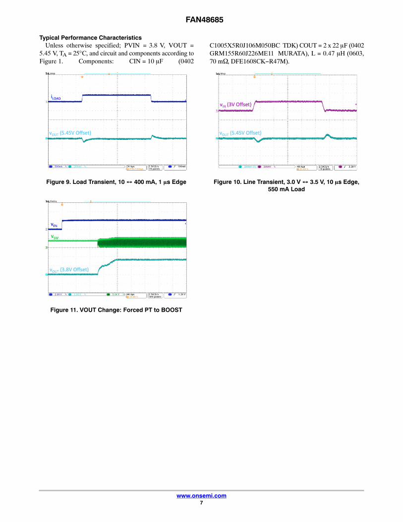
Typical Performance CharacteristicsUnless otherwise specified; PVIN = 3.8 V, VOUT =
5.45 V, TA = 25°C, and circuit and components according toFigure 1. Components: CIN = 10 �F (0402
C1005X5R0J106M050BC TDK) COUT = 2 x 22 �F (0402GRM155R60J226ME11 MURATA), L = 0.47 �H (0603,70 m�, DFE1608CK−R47M).
Figure 9. Load Transient, 10 � 400 mA, 1 �s Edge Figure 10. Line Transient, 3.0 V � 3.5 V, 10 �s Edge,550 mA Load
Figure 11. VOUT Change: Forced PT to BOOST
FAN48685
www.onsemi.com8
APPLICATION INFORMATION
Operation DescriptionThe FAN48685 is low−power boost regulator designed to
provide a minimum voltage regulated rail from a standardsingle−cell Li−Ion battery. The device offers superiorfeatures for NFC applications. PWM switching frequency ismaintain away from the sub carrier of NFC applicationavoiding interference. The FAN48685 automatically goes to100% duty cycle when the input voltage nears the outputvoltage. The part can also be placed in forced pass throughmode by pulling both mode pins low.
Startup Behavior
Startup DescriptionThe device is designed to startup with no load allowing the
implementation of input current controls that support lowercapacity batteries without inducing brown out. Care shouldbe taken in the system design to ensure load is applied afterregulation has been reached and output capacitance is asuitable value to avoid fault time−outs occurring. The devicecan startup in either boost mode or forced pass−throughmode. When starting in boost mode, the part has a linearmode which limits the battery current to 90 mA (typ.) toavoid large inrush currents from the battery. In linear mode,if VOUT fails to reach PVIN target within 1.5 ms, a faultcondition is declared and the device waits 20 ms to attemptan automatic restart. Once VOUT charges up to PVIN, thelinear mode current limit is disabled and the output voltageis ramped to the final value via the DAC that programs theoutput.
When starting up in forced pass−through mode, the outputvoltage is charged using the same linear mode mechanismuntil VOUT reaches PVIN.
Modes of Operation
PWM DescriptionDuring PWM mode, the output voltage is regulated by
switching at a constant frequency and then modulating theenergy per cycle to control the power to the load.
Forced Pass−Through ModeWhen both mode pins are pulled low, the part will be
forced in pass−through mode. The output voltage is around:VOUT = (PVIN − (IOUT* (DCR of L +HIGH SIDE FETRDSON)) during this mode.
Automatic Pass−Through ModeIn normal operation, the device automatically transitions
from boost mode to pass−through mode if PVIN is withinabout 150 mV of VOUT boost voltage. In pass−throughmode, the device has a low impedance path between PVINand VOUT. Entry into pass−through mode occurs whenPVIN is sufficiently close to VOUT that minimum on−timepersists for 16 cycles. In Automatic pass−through mode,there is short−circuit protection which protects both the ICand external components.
Mode Transition
Pass−Through to Boost ModeWhen going from pass−through mode to boost mode,
initially there is a delay for the internal digital circuitry topower up the analog circuitry. After, analog circuitry ispowered, the internal DAC will begin to start stepping from2.45 V. As soon as the internal DAC step is greater thanPVIN, the VOUT of the device begins to increase until itreaches its final VOUT target value. The device is designedto transitions under no load, care should be taken in systemdesign to ensure the load is not applied during VOUTtransitions.
When going from boost mode to pass−through mode, theoutput voltage decay will be determined by the amount ofload at the VOUT.
Boost to Boost ModeWhen going from boost mode to a higher VOUT boost
mode, the internal DAC starts its step from the currentVOUT until the final VOUT target. Since there is no latencyfor the analog to be powered up, immediately after the DACstepping, the VOUT of the device begins to increase until itreaches its final VOUT target value.
When going from boost mode to a lower VOUT boostmode, the output voltage decay will be determined by theamount of load at the VOUT.
Protection Features
VOUT FaultDuring startup, if the VOUT fails to reach PVIN target
within 1.5 ms, the part declares a fault. Once the fault istriggered, the regulator stops switching and presents ahigh−impedance path between PVIN and VOUT.
Current Limit Protection (OCP)FAN48685 has a current limit feature, which protects
itself and load during overloading conditions. When theinductor peak current is reached and held for 2 ms, the devicegoes into a fault. The part restarts every 20 ms once faultoccurs.
Thermal Shutdown Protection (TSP)When the die temperature increases, due to a high load
condition and/or a high ambient temperature; the outputswitching is disabled until the die temperature fallssufficiently. The junction temperature at which the thermalshutdown activates is nominally 150°C with a 15°Chysteresis.
Automatic Pass−Through Mode ProtectionDuring automatic pass−through mode, the device is
short−circuit protected, if the voltage difference betweenPVIN and VOUT exceed more than 300 mV for 10 us, thena fault is declared. The part will restart every 20 ms.

FAN48685
www.onsemi.com9
Under−Voltage Lockout (UVLO)Once PVIN reaches UVLO rising the part will begin to
switch and begin the startup process. When PVIN falls toUVLO falling, the part stops switching and output voltagestarts decays to 0 V.
Control Pin Functionality
Table 8. MODE PINS FUNCTIONALITY (Note 8)
Mode 1 Mode 0 Status of Device
0 0 Forced Pass−Through Mode; VOUT = PVIN
0 1 Active; VOUT = 5.00 V
1 0 Active; VOUT = 3.60 V
1 1 Active; VOUT = 5.45 V
8. Recommended to have logic levels transitions and fall timestypically at 100 ns. MODE Pins have smart pulls down of300 k� (typ.) and are only activated when at logic LOW.

FAN48685
www.onsemi.com10
ADDITIONAL APPLICATIONS INFORMATION
Application Guidelines
Input Capacitor ConsiderationsThe 10 �F ceramic 0402 (1005 metric) input capacitor
should be placed as close as possible between the PVIN pinand GND to minimize the parasitic inductance. If a long wireis used to bring power to the IC, additional “bulk”capacitance (electrolytic or tantalum) should be placed (onEvaluation board) between CIN and the power source leadto reduce the ringing that can occur between the inductanceof the power source leads and CIN. The effectivecapacitance value decreases as PVIN increases due to DCbias effects.
Output Capacitor ConsiderationsThe two 22 �F ceramic 0402 (1005 metric) output
capacitor should be placed as close as possible between theVOUT pin and GND to minimize the parasitic inductance.The effective capacitance value decreases as VOUTincreases due to DC bias effects. Therefore, a minimum 5 uFcapacitance is required to maintain stable regulation at theoutput.
If the output capacitance is increased beyond therecommended two 22 �F ceramic the system design shouldbe evaluated to ensure that the part does not enter fault stateor hiccup during start−up as the device charges the outputcapacitance.
Inductor ConsiderationsThe FAN48685 employs a peak current limiting, so peak
inductor current can reach 3.63 A for a short duration during
overload conditions. Saturation effects causes the inductorcurrent ripple to become higher under high loading, as onlythe peak of the inductor current ripple is controlled.
Layout ConsiderationsThe layout recommendations below highlight various
top−copper pours using different colors. To minimize spikesat VOUT, COUT must be placed as close as possible toPGND and VOUT, as shown in Figure 12.
For thermal reasons, it is suggested to maximize the pourarea for all planes other than SW. Especially the ground pourshould be set to fill all available PCB surface area and tiedto internal layers with a cluster of thermal vias.
Figure 12. Recommended Layout
FAN48685CIN
L
COUTCOUT
FAN48685
www.onsemi.com11
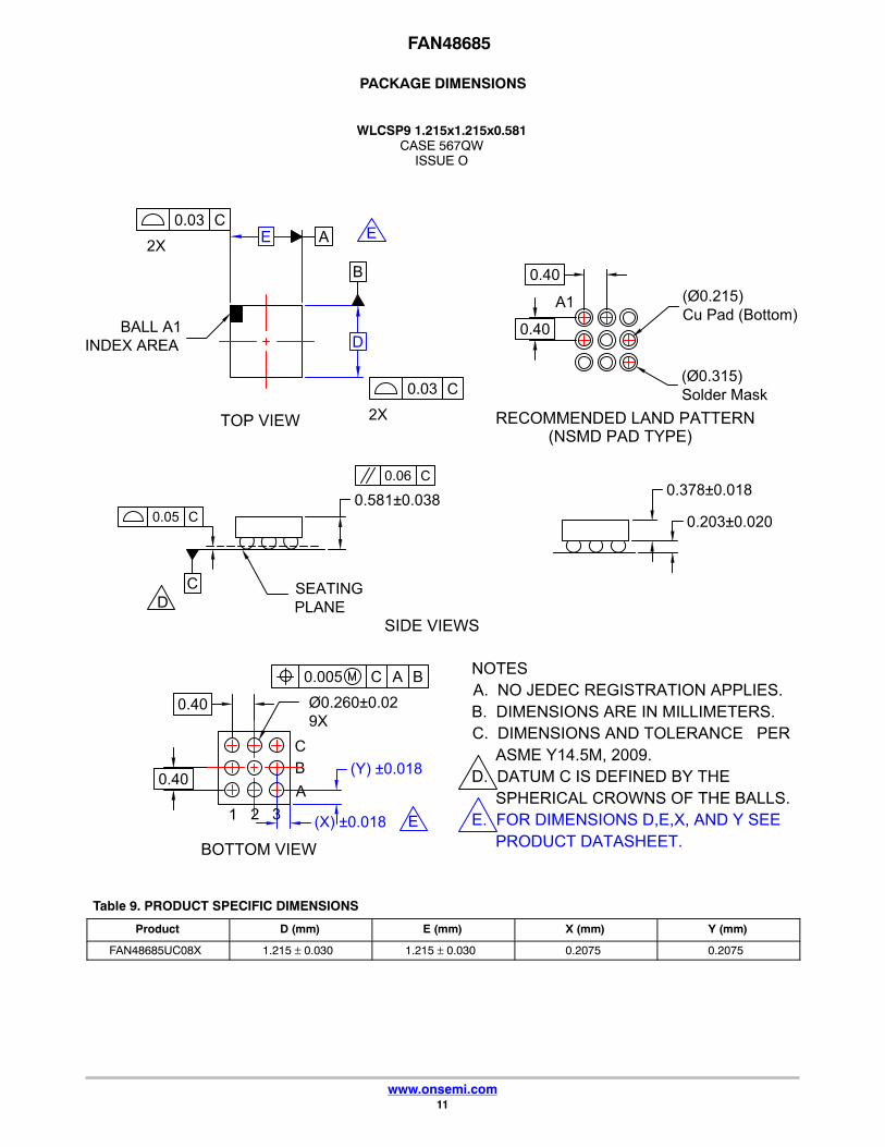
PACKAGE DIMENSIONS
WLCSP9 1.215x1.215x0.581CASE 567QW
ISSUE O
Table 9. PRODUCT SPECIFIC DIMENSIONS
Product D (mm) E (mm) X (mm) Y (mm)
FAN48685UC08X 1.215 ± 0.030 1.215 ± 0.030 0.2075 0.2075
FAN48685
www.onsemi.com12
ON Semiconductor and are trademarks of Semiconductor Components Industries, LLC dba ON Semiconductor or its subsidiaries in the United States and/or other countries.ON Semiconductor owns the rights to a number of patents, trademarks, copyrights, trade secrets, and other intellectual property. A listing of ON Semiconductor’s product/patentcoverage may be accessed at www.onsemi.com/site/pdf/Patent−Marking.pdf. ON Semiconductor reserves the right to make changes without further notice to any products herein.ON Semiconductor makes no warranty, representation or guarantee regarding the suitability of its products for any particular purpose, nor does ON Semiconductor assume any liabilityarising out of the application or use of any product or circuit, and specifically disclaims any and all liability, including without limitation special, consequential or incidental damages.Buyer is responsible for its products and applications using ON Semiconductor products, including compliance with all laws, regulations and safety requirements or standards,regardless of any support or applications information provided by ON Semiconductor. “Typical” parameters which may be provided in ON Semiconductor data sheets and/orspecifications can and do vary in different applications and actual performance may vary over time. All operating parameters, including “Typicals” must be validated for each customerapplication by customer’s technical experts. ON Semiconductor does not convey any license under its patent rights nor the rights of others. ON Semiconductor products are notdesigned, intended, or authorized for use as a critical component in life support systems or any FDA Class 3 medical devices or medical devices with a same or similar classificationin a foreign jurisdiction or any devices intended for implantation in the human body. Should Buyer purchase or use ON Semiconductor products for any such unintended or unauthorizedapplication, Buyer shall indemnify and hold ON Semiconductor and its officers, employees, subsidiaries, affiliates, and distributors harmless against all claims, costs, damages, andexpenses, and reasonable attorney fees arising out of, directly or indirectly, any claim of personal injury or death associated with such unintended or unauthorized use, even if suchclaim alleges that ON Semiconductor was negligent regarding the design or manufacture of the part. ON Semiconductor is an Equal Opportunity/Affirmative Action Employer. Thisliterature is subject to all applicable copyright laws and is not for resale in any manner.
PUBLICATION ORDERING INFORMATIONN. American Technical Support: 800−282−9855 Toll FreeUSA/Canada
Europe, Middle East and Africa Technical Support:Phone: 421 33 790 2910
FAN48685/D
TINYBOOST is a registered trademark of Semiconductor Components Industries, LLC.
LITERATURE FULFILLMENT:Literature Distribution Center for ON Semiconductor19521 E. 32nd Pkwy, Aurora, Colorado 80011 USAPhone: 303−675−2175 or 800−344−3860 Toll Free USA/CanadaFax: 303−675−2176 or 800−344−3867 Toll Free USA/CanadaEmail: [email protected]
ON Semiconductor Website: www.onsemi.com
Order Literature: http://www.onsemi.com/orderlit
For additional information, please contact your localSales Representative
◊