fan 6755 = teot 6755
DESCRIPTION
Ajudando pra ser ajudado. rsTRANSCRIPT

7/21/2019 Fan 6755 = TEOT 6755
http://slidepdf.com/reader/full/fan-6755-teot-6755 1/17
June 2011
© 2009 Fairchild Semiconductor Corporation www.fairchildsemi.comFAN6755W / FAN6755UW • Rev. 1.0.5
F A N 6 7 5 5 W / F A
N 6 7 5 5 UW—
mW S av er ™
C
on t r ol l er
FAN6755W / FAN6755UWmWSaver ™
PWM Controller
Features
mWSaver ™
Technology Provides Industry’s Best-in-Class Standby Power
o <100mW at 25mW Load for LCDM Adaptor
o Internal High-Voltage JFET Startup
o Low Operating Current Maximum: 2mA
o Adaptive Decreasing of PWM Frequency to23KHz at Light-Load Condition, ImprovedLight-Load Efficiency
o Feedback Impedance Switching DuringMinimum Load or No Load
Proprietary Asynchronous Frequency HoppingReduced EMI
Fixed PWM Frequency: 65KHz (FAN6755W),130KHz (FAN6755UW)
Internal Leading-Edge Blanking
Built-in Synchronized Slope Compensation
Auto-Restart Protection: Feedback Open-LoopProtection (OLP), VDD Over-Voltage Protection(OVP), Over-Temperature Protection (OTP), andLine Over-Voltage Protection
Soft Gate Drive with Clamped Output Voltage: 18V
VDD Under-Voltage Lockout (UVLO)
Programmable Constant Power Limit (Full ACInput Range)
Internal OTP Sensor with Hysteresis
Build-in 5ms Soft-Start Function
Input Voltage Sensing (VIN Pin) for Brown-In/OutProtection with Hysteresis and Line Over-VoltageProtection
Appl ications
General-purpose switched-mode power supplies andflyback power converters, including:
LCD Monitor Power Supply
Open-Frame SMPS
Description
This highly integrated PWM controller provides severalfeatures to enhance the performance of flybackconverters.
To minimize standby power consumption, a proprietaryadaptive green-mode function reduces switchingfrequency at light-load condition. To avoid acoustic-noise problems, the minimum PWM frequency is setabove 23kHz. This green-mode function enables thepower supply to meet international power conservationrequirements, such as Energy Star ®. With the internalhigh-voltage startup circuitry, the power loss caused bybleeding resistors is also eliminated. To further reducepower consumption, FAN6755W/UW uses the BiCMOSprocess, which allows an operating current of only 2mA.The standby power consumption can be under 100mWfor most of LCD monitor power supply designs.
FAN6755W/UW integrates a frequency-hopping functionthat reduces EMI emission of a power supply withminimum line filters. Its built-in synchronized slopecompensation achieves a stable peak-current-modecontrol and improves noise immunity. The proprietary,external line compensation ensures constant outputpower limit over a wide AC input voltage range from90V AC to 264V AC.
FAN6755W/UW provides many protection functions.The internal feedback open-loop protection circuitprotects the power supply from open feedback loopcondition or output short condition. It also has lineunder-voltage protection (brownout protection) and over-voltage protection using an input voltage sensing pin(VIN).
FAN6755W/UW is available in a 7-pin SOP package.
ENERGY STAR® is a registered trademark of the U.S. Department of Energy and the U.S. Environmental Protection Agency.
7/21/2019 Fan 6755 = TEOT 6755
http://slidepdf.com/reader/full/fan-6755-teot-6755 2/17
© 2009 Fairchild Semiconductor Corporation www.fairchildsemi.comFAN6755W / FAN6755UW • Rev. 1.0.5 2
F A N 6 7 5 5 W / F A
N 6 7 5 5 UW—
mW S av er ™
C
on t r ol l er
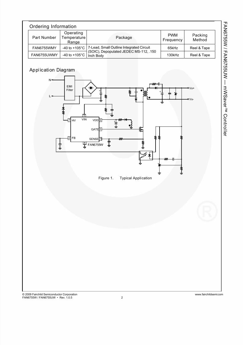
Ordering Information
Part NumberOperating
TemperatureRange
PackagePWM
FrequencyPackingMethod
FAN6755WMY -40 to +105°C 7-Lead, Small Outline Integrated Circuit(SOIC), Depopulated JEDEC MS-112, .150Inch Body
65kHz Reel & Tape
FAN6755UWMY -40 to +105°C 130kHz Reel & Tape
Appl ication Diagram
Figure 1. Typical Appli cation

7/21/2019 Fan 6755 = TEOT 6755
http://slidepdf.com/reader/full/fan-6755-teot-6755 3/17
© 2009 Fairchild Semiconductor Corporation www.fairchildsemi.comFAN6755W / FAN6755UW • Rev. 1.0.5 3
F A N 6 7 5 5 W / F A
N 6 7 5 5 UW—
mW S av er ™
C
on t r ol l er
Internal Block Diagram
Figure 2. Internal Block Diagram
Marking Information
Figure 3. Top Mark
Z: Plant CodeX: 1-Digit Year CodeY: 1-Digit Week CodeTT: 2-Digit Die Run CodeT: Package Type (M:SOP)P: Y=Green PackageM: Manufacture Flow Code
ZXYTT6755WTPM
7
ZXYTT6755UWTPM
7
GATE
FB
SENSE
GND
VDD
VIN 1
5.3V
SoftDriver
QS
R
5.3V
UVLO
Green
Mode BlankingCircuit
OLP
OVP
Delay
Debounce
VDD-OVP
6
7
5
2
3
HV
Brownout Protection
OLP
3R
OLP
Comparator
PWM
Comparator
Internal
BIAS
Soft-Start
VLimit
SlopeCompensation
R
Current Limit
Comparator
Soft-Start
Comparator
4
VIN_ON / VIN_OFF
VLimit
Brownout Protection
High/Low
Line Compensation
Debounce
OLPRe-start
ProtectionOVP
VDD
OTP
V D D - O N
/ V D D - O F F
VFB-OLP
OTP
VIN-Protect
VIN-Protect
HVStartup
Clock
Generator
…

7/21/2019 Fan 6755 = TEOT 6755
http://slidepdf.com/reader/full/fan-6755-teot-6755 4/17
© 2009 Fairchild Semiconductor Corporation www.fairchildsemi.comFAN6755W / FAN6755UW • Rev. 1.0.5 4
F A N 6 7 5 5 W / F A
N 6 7 5 5 UW—
mW S av er ™
C
on t r ol l er
Pin Configuration
Figure 4. Pin Configu ration (Top View)
Pin Definitions
Pin # Name Descript ion
1 VIN
Line-voltage detection. The line-voltage detection is used for brownout protection with hysteresis.Constant output power limit over universal AC input range is also achieved using this VIN pin. It
is suggested to add a low-pass filter to filter out line ripple on the bulk capacitor. Pulling VINHIGH also triggers auto-restart protection.
2 FBThe signal from the external compensation circuit is fed into this pin. The PWM duty cycle isdetermined in response to the signal on this pin and the current-sense signal on the SENSE pin.
3 SENSECurrent sense. The sensed voltage is used for peak-current-mode control and cycle-by-cyclecurrent limiting.
4
GND Ground
5 GATE The totem-pole output driver. Soft-driving waveform is implemented for improved EMI.
6 VDDPower supply. The internal protection circuit disables PWM output as long as VDD exceeds theOVP trigger point.
7 HV For startup, this pin is pulled HIGH to the line input or bulk capacitor via resistors.
SOP-7
VIN
VDD
GATE
HV
GND
SENSE
FB
1 7
6
54
2
3
7/21/2019 Fan 6755 = TEOT 6755
http://slidepdf.com/reader/full/fan-6755-teot-6755 5/17
© 2009 Fairchild Semiconductor Corporation www.fairchildsemi.comFAN6755W / FAN6755UW • Rev. 1.0.5 5
F A N 6 7 5 5 W / F A
N 6 7 5 5 UW—
mW S av er ™
C
on t r ol l er
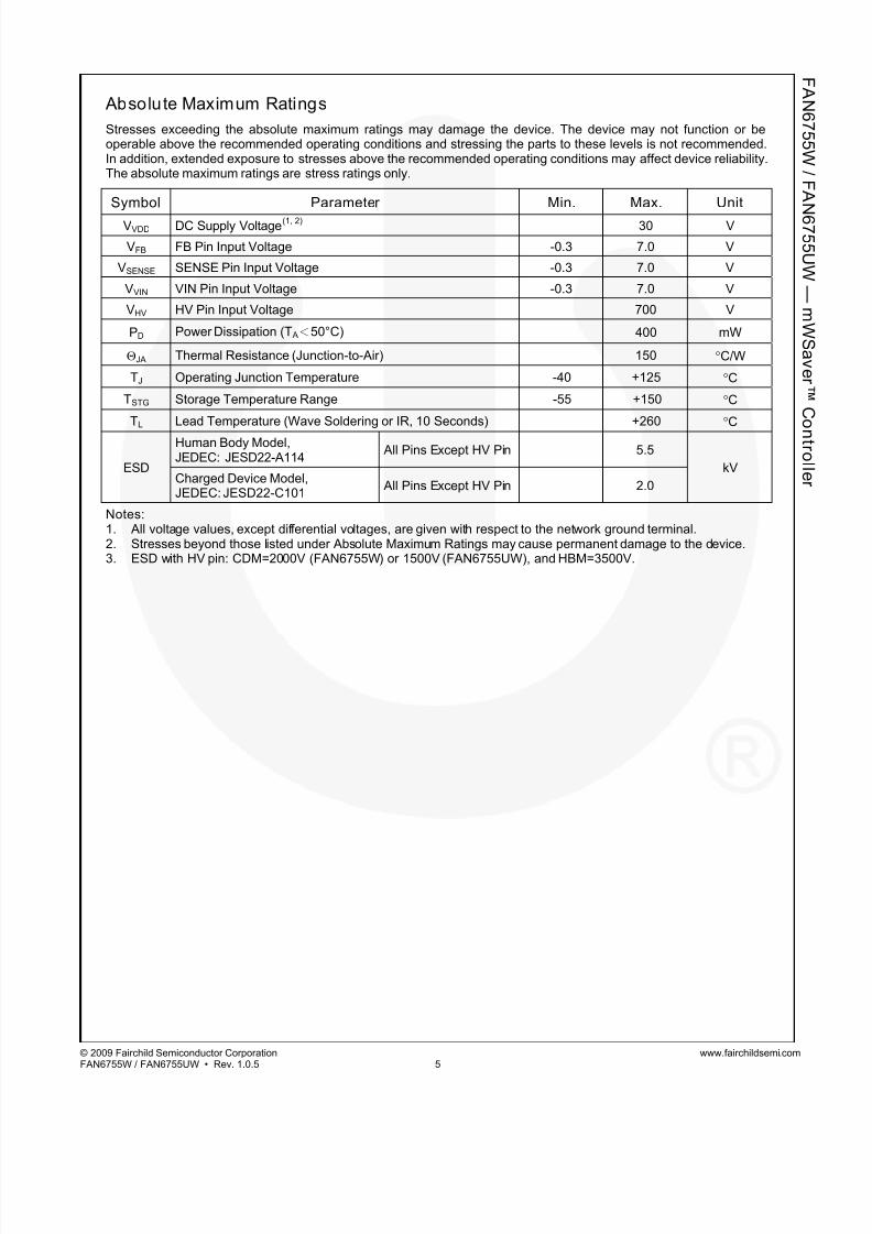
Absolute Maximum Ratings
Stresses exceeding the absolute maximum ratings may damage the device. The device may not function or beoperable above the recommended operating conditions and stressing the parts to these levels is not recommended.In addition, extended exposure to stresses above the recommended operating conditions may affect device reliability.The absolute maximum ratings are stress ratings only.
Symbol Parameter Min. Max. Unit
VVDD DC Supply Voltage(1, 2)
30 V
VFB FB Pin Input Voltage -0.3 7.0 V
VSENSE SENSE Pin Input Voltage -0.3 7.0 V
VVIN VIN Pin Input Voltage -0.3 7.0 V
VHV HV Pin Input Voltage 700 V
PD Power Dissipation (T A<50°C) 400 mW
JA Thermal Resistance (Junction-to-Air) 150 C/W
TJ Operating Junction Temperature -40 +125 C
TSTG Storage Temperature Range -55 +150 C
TL Lead Temperature (Wave Soldering or IR, 10 Seconds) +260 C
ESD
Human Body Model,JEDEC: JESD22-A114
All Pins Except HV Pin 5.5
kVCharged Device Model,JEDEC: JESD22-C101
All Pins Except HV Pin 2.0
Notes:1. All voltage values, except differential voltages, are given with respect to the network ground terminal.2. Stresses beyond those listed under Absolute Maximum Ratings may cause permanent damage to the device.3. ESD with HV pin: CDM=2000V (FAN6755W) or 1500V (FAN6755UW), and HBM=3500V.
7/21/2019 Fan 6755 = TEOT 6755
http://slidepdf.com/reader/full/fan-6755-teot-6755 6/17
© 2009 Fairchild Semiconductor Corporation www.fairchildsemi.comFAN6755W / FAN6755UW • Rev. 1.0.5 6
F A N 6 7 5 5 W / F A
N 6 7 5 5 UW—
mW S av er ™
C
on t r ol l er
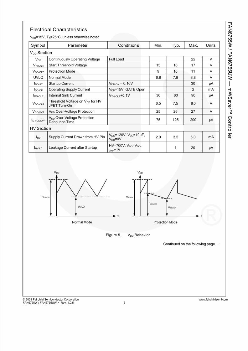
Electrical Characteristics
VDD=15V, T A=25C, unless otherwise noted.
Symbol Parameter Condit ions Min. Typ. Max. Units
VDD Section
VOP
Continuously Operating Voltage Full Load 22 V
VDD-ON Start Threshold Voltage 15 16 17 V
VDD-OFF Protection Mode 9 10 11 V
UVLO Normal Mode 6.8 7.8 8.8 V
IDD-ST Startup Current VDD-ON – 0.16V 30 µA
IDD-OP Operating Supply Current VDD=15V, GATE Open 2 mA
IDD-OLP Internal Sink Current VTH-OLP+0.1V 30 60 90 µA
VDD-OLP Threshold Voltage on VDD for HVJFET Turn-On
6.5 7.5 8.0 V
VDD-OVP VDD Over-Voltage Protection 25 26 27 V
tD-VDDOVP VDD Over-Voltage Protection
Debounce Time
75 125 200 µs
HV Section
IHV Supply Current Drawn from HV PinVDC=120V, VDD=10µF,VDD=0V
2.0 3.5 5.0 mA
IHV-LC Leakage Current after StartupHV=700V, VDD=VDD-
OFF+1V1 20 µ A
Figure 5. VDD Behavior
Continued on the following page…

7/21/2019 Fan 6755 = TEOT 6755
http://slidepdf.com/reader/full/fan-6755-teot-6755 7/17
© 2009 Fairchild Semiconductor Corporation www.fairchildsemi.comFAN6755W / FAN6755UW • Rev. 1.0.5 7
F A N 6 7 5 5 W / F A
N 6 7 5 5 UW—
mW S av er ™
C
on t r ol l er
Electrical Characteristics
VDD=15V, T A=25C, unless otherwise noted.
Symbol Parameter Condit ions Min. Typ. Max. Units
Oscillator Section
f OSC Frequency in Normal Mode
CenterFrequency
FAN6755W 62 65 68
KHzFAN6755UW 124 130 136
HoppingRange
FAN6755W ±4.5 ±5.2 ±5.9
FAN6755UW ±9 ±10.4 ±11.8
f OSC-G Green-Mode Frequency 20 23 26 KHz
tHOP Hopping Period 10.00 12.00 14.00 ms
f DV Frequency Variation vs. VDD Deviation
VDD=11V to 22V 5 %
f DT Frequency Variation vs.Temperature Deviation
T A=-40 to 85C=TJ 5 %
VIN Section
VIN-OFF PWM Turn-Off Threshold Voltage 0.66 0.70 0.74 V
VIN-ON PWM Turn-On Threshold VoltageVIN-OFF+
0.17
VIN-OFF+
0.20
VIN-OFF+
0.23V
VIN-Protect PWM Protect Threshold Voltage 5.1 5.3 5.5 V
tVIN-Protect PWM Protect Debounce Time 60 100 140 µs
Current-Sense Section
VTH-P atVIN=1V
Threshold Voltage for Current Limit VIN=1V 0.80 0.83 0.86 V
VTH-P atVIN=3V
Threshold Voltage for Current Limit VIN=3V 0.67 0.70 0.73 V
tPD Delay to Output 100 200 ns
tLEB Leading-Edge Blanking TimeSoft-Start (FAN6755UW) 125 150 175
nsSteady State 240 290 340
tSS Period During Soft-Start Time Startup Time 4.0 5.5 7.0 ms
Figure 6. VIN vs. VSENSE
Continued on the following page…

7/21/2019 Fan 6755 = TEOT 6755
http://slidepdf.com/reader/full/fan-6755-teot-6755 8/17
© 2009 Fairchild Semiconductor Corporation www.fairchildsemi.comFAN6755W / FAN6755UW • Rev. 1.0.5 8
F A N 6 7 5 5 W / F A
N 6 7 5 5 UW—
mW S av er ™
C
on t r ol l er
Electrical Characteristics
VDD=15V, T A=25C, unless otherwise noted.
Symbol Parameter Condit ions Min. Typ. Max. Units
Feedback Input Section
AV Input Voltage to Current-Sense
Attenuation 1/4.5 1/4.0 1/3.5 V/V
ZFB Input Impedance VFB=4V 10 15 19 kΩ
VFB-OPEN Output High Voltage FB Pin Open 5.1 5.3 5.5 V
VFB-OLP FB Open-Loop Trigger Level 4.4 4.6 4.8 V
tD-OLP Delay Time of FB Pin Open-loopProtection
45.0 62.5 70.0 ms
VFB-N Green-Mode Entry FB Voltage 2.8 3.0 3.2 V
VFB-G Green-Mode Ending FB Voltage VFB-N - 0.6 V
VFB-ZDCR FB Threshold Voltage for Zero-DutyRecovery
1.6 1.8 2.0 V
VFB-ZDC FB Threshold Voltage for Zero-Duty 1.4 1.6 1.8 V
VFB-ZDCR -
VFB-ZDC ZDC Hysterisis 0.12 0.15 0.19 V
Figure 7. VFB vs. PWM Frequency
Continued on the following page…

7/21/2019 Fan 6755 = TEOT 6755
http://slidepdf.com/reader/full/fan-6755-teot-6755 9/17
© 2009 Fairchild Semiconductor Corporation www.fairchildsemi.comFAN6755W / FAN6755UW • Rev. 1.0.5 9
F A N 6 7 5 5 W / F A
N 6 7 5 5 UW—
mW S av er ™
C
on t r ol l er
Electrical Characteristics
VDD=15V, T A=25C, unless otherwise noted.
Symbol Parameter Condit ions Min. Typ. Max. Units
GATE Section
DCYMAX
Maximum Duty Cycle 60 75 90 %
VGATE-L Gate Low Voltage VDD=15V, IO=50mA 1.5 V
VGATE-H Gate High Voltage VDD=12V, IO=50mA 8 V
tr Gate Rising Time VDD=15V, CL=1nF 100 ns
tf Gate Falling Time VDD=15V, CL=1nF 30 ns
IGATE-
SOURCE Gate Source Current VDD=15V, GATE=6V 700 mA
VGATE-
CLAMP_1 Gate Output Clamping Voltage VDD=22V 18 V
Over-Temperature Protection Section (OTP)
TOTP Protection Junction Temperature(4,6)
140 °C
TRestart Restart Junction Temperature(5,6)
TOTP-25 °CNotes:4. When activated, the output is disabled and the latch is turned off.5. The threshold temperature for enabling the output again and resetting the latch after over-temperature protection
has been activated.6. These parameters are guaranteed by design.

7/21/2019 Fan 6755 = TEOT 6755
http://slidepdf.com/reader/full/fan-6755-teot-6755 10/17
© 2009 Fairchild Semiconductor Corporation www.fairchildsemi.comFAN6755W / FAN6755UW • Rev. 1.0.5 10
F A N 6 7 5 5 W / F A
N 6 7 5 5 UW—
mW S av er ™
C
on t r ol l er
Typical Performance Characteristics
Figure 8. Startup Current (IDD-ST) vs. TemperatureFigure 9. Operation Supply Current (IDD-OP)
vs. Temperature
Figure 10. Start Threshold Voltage (VDD-ON)
vs. Temperature
Figure 11. Minimum Operating Voltage (VDD-OFF)
vs. Temperature
Figure 12. Supply Cur rent Drawn from HV Pin (IHV)
vs. Temperature
Figure 13. HV Pin Leakage Current After Startup
(IHV-LC) vs. Temperature
Figure 14. Frequency in Normal Mode (f OSC)
vs. Temperature
Figure 15. Maximum Duty Cycle (DCYMAX)
vs. Temperature

7/21/2019 Fan 6755 = TEOT 6755
http://slidepdf.com/reader/full/fan-6755-teot-6755 11/17
© 2009 Fairchild Semiconductor Corporation www.fairchildsemi.comFAN6755W / FAN6755UW • Rev. 1.0.5 11
F A N 6 7 5 5 W / F A
N 6 7 5 5 UW—
mW S av er ™
C
on t r ol l er
Typical Performance Characteristics
Figure 16. FB Open-Loop Trigger Level (VFB-OLP)
vs. Temperature
Figure 17. Delay Time of FB Pin Open-Loop Protection
(tD-OLP) vs. Temperature
Figure 18. PWM Turn-Off Threshold Voltage
(VIN-OFF & VIN-ON) vs. Temperature
Figure 19. VDD Over-Voltage Protection (VDD-OVP)
vs. Temperature
Figure 20. VIN vs. VLIMIT

7/21/2019 Fan 6755 = TEOT 6755
http://slidepdf.com/reader/full/fan-6755-teot-6755 12/17
© 2009 Fairchild Semiconductor Corporation www.fairchildsemi.comFAN6755W / FAN6755UW • Rev. 1.0.5 12
F A N 6 7 5 5 W / F A
N 6 7 5 5 UW—
mW S av er ™
C
on t r ol l er
Functional Description
Startup Current
For startup, the HV pin is connected to the line input(1N4007 / 100KΩ recommended) or bulk capacitorthrough a resistor, RHV. Startup current drawn from pin
HV (typically 3.5mA) charges the hold-up capacitorthrough the diode and resistor. When the VDD capacitorlevel reaches VDD-ON, the startup current switches off. Atthis moment, the VDD capacitor only supplies theFAN6755W/UW to maintain VDD before the auxiliarywinding of the main transformer to provide the operatingcurrent.
Operating Current
Operating current is around 2mA. The low operatingcurrent enables better efficiency and reduces therequirement of VDD hold-up capacitance.
Green-Mode Operation
The proprietary green-mode function provides an off-time modulation to reduce the switching frequency inlight-load and no-load conditions. The on time is limitedfor better abnormal or brownout protection. VFB, which isderived from the voltage feedback loop, is taken as thereference. Once VFB is lower than the threshold voltage,switching frequency is continuously decreased to theminimum green-mode frequency of around 23KHz.
Current Sensing / PWM Current Limit ing
Peak-current-mode control is utilized to regulate outputvoltage and provide pulse-by-pulse current limiting. Theswitch current is detected by a sense resistor into theSENSE pin. The PWM duty cycle is determined by this
current sense signal and VFB, the feedback voltage.When the voltage on the SENSE pin reaches aroundVCOMP=(VFB –0.6)/4, a switch cycle is terminatedimmediately. VCOMP is internally clamped to a variablevoltage around 0.83V for output power limit.
Leading-Edge Blanking (LEB)
Each time the power MOSFET is switched on, a turn-onspike occurs on the sense resistor. To avoid prematuretermination of the switching pulse, a leading-edgeblanking time is built in. During this blanking period, thecurrent-limit comparator is disabled and cannot switchoff the gate driver.
Under-Voltage Lockout (UVLO)
The turn-on and turn-off thresholds are fixed internally at16V and 7.8V in normal mode. During startup, the hold-up capacitor must be charged to 16V through the startupresistor to enable the IC. The hold-up capacitorcontinues to supply VDD before the energy can bedelivered from auxiliary winding of the main transformer.VDD must not drop below 7.8V during startup. ThisUVLO hysteresis window ensures that the hold-upcapacitor is adequate to supply VDD during startup.
Gate Outpu t / Soft Driv ing
The BiCMOS output stage is a fast totem-pole gatedriver. Cross conduction has been avoided to minimizeheat dissipation, increase efficiency, and enhance
reliability. The output driver is clamped by an internal18V Zener diode to protect power MOSFET transistorsagainst undesirable gate over voltage. A soft drivingwaveform is implemented to minimize EMI.
Soft-Start
For many applications, it is necessary to minimize theinrush current at startup. The built-in 5.5ms soft-startcircuit significantly reduces the startup current spike andoutput voltage overshoot.
Slope Compensation
The sensed voltage across the current-sense resistor isused for peak-current-mode control and pulse-by-pulse
current limiting. Built-in slope compensation improvesstability and prevents sub-harmonic oscillation.FAN6755W/UW inserts a synchronized positive-goingramp at every switching cycle.
Constant Output Power Limit
For constant output power limit over universal input-voltage range, the peak-current threshold is adjusted bythe voltage of the VIN pin. Since the VIN pin isconnected to the rectified AC input line voltage throughthe resistive divider, a higher line voltage generates ahigher VIN voltage. The threshold voltage decreases asVIN increases, making the maximum output power athigh-line input voltage equal to that at low-line input. The
value of R-C network should not be so large that itaffects the power limit (shown in Figure 21). R and C
should be less than 100 and 470pF, respectively.
Figure 21. Current-Sense R-C Filter

7/21/2019 Fan 6755 = TEOT 6755
http://slidepdf.com/reader/full/fan-6755-teot-6755 13/17
© 2009 Fairchild Semiconductor Corporation www.fairchildsemi.comFAN6755W / FAN6755UW • Rev. 1.0.5 13
F A N 6 7 5 5 W / F A
N 6 7 5 5 UW—
mW S av er ™
C
on t r ol l er
VDD Over-Voltage Protect ion
VDD over-voltage protection prevents damage due toabnormal conditions. Once the VDD voltage is over theover-voltage protection voltage (VDD-OVP), and lasts fortD-VDDOVP, the PWM pulses are disabled. When the VDD voltage drops below the UVLO, PWM pulses start again.Over-voltage conditions are usually caused by openfeedback loops.
Brownout Protection
Since the VIN pin is connected through a resistivedivider to the rectified AC input line voltage, it can alsobe used for brownout protection. If VIN is less than 0.7V,the PWM output is shut off. When VIN reaches over0.9V, the PWM output is turned on again. Thehysteresis window for ON/OFF is around 0.2V. Thebrownout voltage setting is determined by the potentialdivider formed with RUpper and RLower . Equations tocalculate the resistors are shown below:
)Vunit(,VRR
RV AC
Upper Lower
Lower IN
2 (1)
Thermal Overload Protection
Thermal overload protection limits total powerdissipation. When the junction temperature exceeds TJ=
+135C, the thermal sensor signals the shutdown logicand turns off most of the internal circuitry. The thermalsensor turns internal circuitry on again after the IC’s
junction temperature drops by 25C. Thermal overloadprotection is designed to protect the FAN6755W/UW inthe event of a fault condition. For continual operation, donot exceed the absolute maximum junction temperature
of TJ = +150C.
Limited Power Control
The FB voltage is saturated HIGH when the powersupply output voltage drops below its nominal value andshut regulator (KA431) does not draw current throughthe opto-coupler. This occurs when the output feedbackloop is open or output is short circuited. If the FB voltageis higher than a built-in threshold for longer than tD-OLP,PWM output is turned off. As PWM output is turned off,
VDD begins decreasing since no more energy isdelivered from the auxiliary winding.
When VDD goes below the turn-off threshold (~7.5V), thecontroller is totally shut down. VDD is charged up to theturn-on threshold voltage of 16V through the startupresistor until PWM output is restarted. This protectionfeature continues as long as the over loading conditionpersists. This prevents the power supply fromoverheating due to overloading conditions.
Noise Immunity
Noise on the current sense or control signal may causesignificant pulse-width jitter, particularly in continuous-
conduction mode. Slope compensation helps alleviatethis problem. Good placement and layout practicesshould be followed. Avoiding long PCB traces andcomponent leads, locating compensation and filtercomponents near the FAN6755W/UW, and increasingthe power MOS gate resistance improve performance.

7/21/2019 Fan 6755 = TEOT 6755
http://slidepdf.com/reader/full/fan-6755-teot-6755 14/17
© 2009 Fairchild Semiconductor Corporation www.fairchildsemi.comFAN6755W / FAN6755UW • Rev. 1.0.5 14
F A N 6 7 5 5 W / F A
N 6 7 5 5 UW—
mW S av er ™
C
on t r ol l er
Appl ications Information
2
1
3
4
BD1
F1
+
C11
R9
C17
R19
C16
R18
1
2
3
Q1
R28
R12
2
1
D4
+C18
C4
2
1
D3
1
2
4
3
U2
A
K
R U3
R21 C20
R26
R23 R24
12V 5V
R20
+ C8 + C9
12V
+ C14
5VR5
R7 C7
C6
12
3
CN1
AC IN
1
3
2
D5
1
3
2
D1
R6
R4
1 2L2
1 2L3
R16
7
10
2
16
4 1211
9
8
TX1
1
2 3
4
L1
C5
M1
2
1
D2 R11
C15
C10
R1
R2
C3
C1
C2
R8
R17
L
N
N1 N2
N3
N4
N5 N6
N7
N8
N9
VDDFB
SENSE
GATE
HV
N10
N12 N13
N14 N15
N16
N17
N18
N20
N21
N1A
N28
N29
P1
12V
P2
5V
P3
SGN
+ C13
C19
R15
12V1
R27
R25
R13
R10
N30
C12
R3
R14VIN
VIN
2
1
ZD1
R22
5V1
5V1
VIN1
FB2
SENSE3
GND4
GATE 5
VDD 6
HV 7
U1
FAN6755FAN6755W
Figure 22. 44W Flyback 12V/2A, 5V/4A Application Circuit

7/21/2019 Fan 6755 = TEOT 6755
http://slidepdf.com/reader/full/fan-6755-teot-6755 15/17
© 2009 Fairchild Semiconductor Corporation www.fairchildsemi.comFAN6755W / FAN6755UW • Rev. 1.0.5 15
F A N 6 7 5 5 W / F A
N 6 7 5 5 UW—
mW S av er ™
C
on t r ol l er
Build of Materials
Designator Part Type Designator Part Type
BD1 BD 4A/600V Q1 MOS 9A/600V
C1 YC 2200pF/Y1 R1 R 1.5M 1/4W
C2 YC 2200pF/Y1 R2 R 1.5M 1/4W
C3 XC 0.33µF/300V R3 R 10M 1/4W
C4 NC R4, R5, R6, R7 R 47 1/4W
C5 YC 2200pF/Y1 R8, R17, R25, R27 NC
C6 CC 2200pF/100V R9 R 50K 1/4W
C7 CC 1000pF/100V R10 R 50K 1/4W
C8 EC 1000µF/25V R11 R 0 1/8W
C9 EC 470µF/25V R12 R 47 1/8W
C10 CC 100pF/50V R13 R 100K 1/8W
C11 EC 100µF/400V R14 R 0 1/4W
C12 C 1µF/50V R15 R 10K 1/8W
C13 EC 1000µF/10V R16 R 1 1/8W
C14 EC 470µF/10V R18 R 0 1/8W
C15 CC 100pF/50V R19 R 100 1/8W
C16 C 1nF/50V R20 R 1K 1/8W
C17 C 470pF/50V R21 R 4.7K 1/8W
C18 EC 47µF/50V R22 R 7.5K 1/8W
C19 C 0.01µF/50V R23 R 120K 1/8W
C20 C 0.1µF/50V R24 R 15K 1/8W
D1 FYP1010 R26 R 10K 1/8W
D2 1N4148 R28 R 0.43 2W
D3 FR107 TX1 800µH(ERL-28)
D4 FR103 U1 IC FAN6755W
D5 FYP1010 U2 IC PC817
ZD1 P6KE150A U3 IC TL431
F1 FUSE 4A/250V
M1 VZ 9G
L1 13mH
L2 Inductor (2µH)
L3 Inductor (2µH)

7/21/2019 Fan 6755 = TEOT 6755
http://slidepdf.com/reader/full/fan-6755-teot-6755 16/17
© 2009 Fairchild Semiconductor Corporation www.fairchildsemi.comFAN6755W / FAN6755UW • Rev. 1.0.5 16
F A N 6 7 5 5 W / F A
N 6 7 5 5 UW—
mW S av er ™
C
on t r ol l er
Physical Dimensions
8¢X0¢X
SEE DETAIL A
LAND PATTERN RECOMMENDATION
SEATING PLANE
0.10 C
C
GAGE PLANE
x 45¢X
DETAIL ASCALE: 2:1
PIN ONE
INDICATOR
4
8
1
CM B A0.25
B5
A
3.85
0.65TYP
1.75TYP
1.27
6.205.80
3.81
4.003.80
5.004.80
(0.33)1.27
0.51
0.33
0.25
0.10
1.75 MAX0.250.19
0.36
0.500.25
R0.10
R0.10
0.90
0.406 (1.04)
OPTION A - BEVEL EDGE
OPTION B - NO BEVEL EDGE
7.35
3.81
NOTES: UNLESS OTHERWISE SPECIFIED
A) THIS PACKAGE CONFORMS TO JEDEC
MS-012, VARIATION AA, ISSUE C,
DATED MAY 1990 EXCEPT PIN# 7 IS REMOVED.
B) ALL DIMENSIONS ARE IN MILLIMETERS.
C) DIMENSIONS DO NOT INCLUDE MOLD
FLASH OR BURRS.
D) STANDARD LEAD FINISH:
200 MICROINCHES / 5.08 MICRONS MIN.
LEAD/TIN (SOLDER) ON COPPER.
E) DRAWING FILENAME : M07AREV2
Figure 23. 7-Lead, Small Outl ine Package (SOP)
Package drawings are provided as a service to customers considering Fairchild components. Drawings may change in any mannerwithout notice. Please note the revision and/or date on the drawing and contact a Fairchild Semiconductor representative to verify orobtain the most recent revision. Package specifications do not expand the terms of Fairchild’s worldwide terms and conditions,specifically the warranty therein, which covers Fairchild products.
Always visit Fairchild Semiconductor’s online packaging area for the most recent package drawings:http://www.fairchildsemi.com/packaging/.
7

7/21/2019 Fan 6755 = TEOT 6755
http://slidepdf.com/reader/full/fan-6755-teot-6755 17/17
© 2009 Fairchild Semiconductor Corporation www.fairchildsemi.comFAN6755W / FAN6755UW • Rev 1 0 5 17
F A N 6 7 5 5 W / F A
N 6 7 5 5 UW—
mW S av er ™
C
on t r ol l er