fall 2006ee 5301 - vlsi design automation i v-1 ee 5301 – vlsi design automation i kia bazargan...
Post on 20-Dec-2015
229 views
TRANSCRIPT
Fall 2006 EE 5301 - VLSI Design Automation I V-1
EE 5301 – VLSI Design Automation IEE 5301 – VLSI Design Automation I
Kia Bazargan
University of Minnesota
Part V: PlacementPart V: Placement
Fall 2006 EE 5301 - VLSI Design Automation I V-2
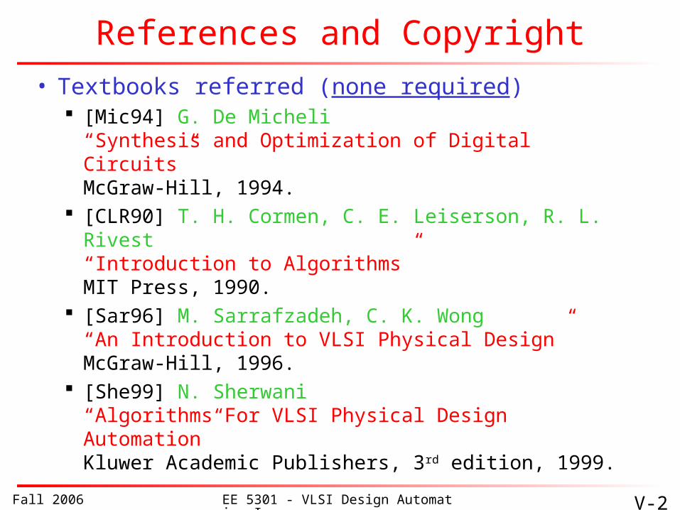
References and Copyright
• Textbooks referred (none required) [Mic94] G. De Micheli
“Synthesis and Optimization of Digital Circuits”McGraw-Hill, 1994.
[CLR90] T. H. Cormen, C. E. Leiserson, R. L. Rivest“Introduction to Algorithms”MIT Press, 1990.
[Sar96] M. Sarrafzadeh, C. K. Wong“An Introduction to VLSI Physical Design”McGraw-Hill, 1996.
[She99] N. Sherwani“Algorithms For VLSI Physical Design Automation”Kluwer Academic Publishers, 3rd edition, 1999.

Fall 2006 EE 5301 - VLSI Design Automation I V-3
References and Copyright (cont.)
• Slides used: (Modified by Kia when necessary) [©Sarrafzadeh] © Majid Sarrafzadeh, UCLA [©Sherwani] © Naveed A. Sherwani, 1992
(companion slides to [She99]) [©Keutzer] © Kurt Keutzer, UC-Berekeley
http://www-cad.eecs.berkeley.edu/~niraj/ee244/index.htm
[©Gupta] © Rajesh Gupta, UC-Irvinehttp://www.ics.uci.edu/~rgupta/ics280.html
[©Kang] © Steve Kang, UIUChttp://www.ece.uiuc.edu/ece482/
[©He] © Lei He, UCLAhttp://eda.ee.ucla.edu/EE201A-04Spring/(ack on Lei’s slides: Thanks to Chis Chu, Jason Cong, Paul Villarubia and David Pan for contributions to slides)
Fall 2006 EE 5301 - VLSI Design Automation I V-4
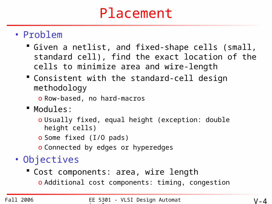
Placement
• Problem Given a netlist, and fixed-shape cells (small,
standard cell), find the exact location of the cells to minimize area and wire-length
Consistent with the standard-cell design methodology
o Row-based, no hard-macros
Modules:o Usually fixed, equal height (exception: double height
cells)o Some fixed (I/O pads)o Connected by edges or hyperedges
• Objectives Cost components: area, wire length
o Additional cost components: timing, congestion
Fall 2006 EE 5301 - VLSI Design Automation I V-5
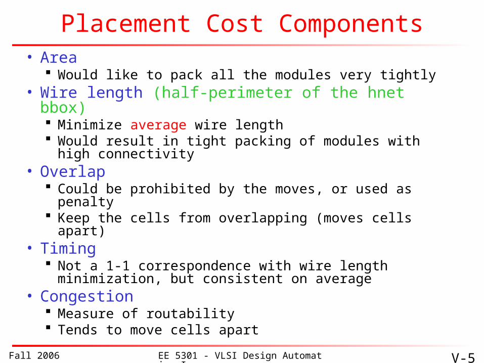
Placement Cost Components• Area
Would like to pack all the modules very tightly• Wire length (half-perimeter of the hnet bbox)
Minimize average wire length Would result in tight packing of modules with high
connectivity• Overlap
Could be prohibited by the moves, or used as penalty
Keep the cells from overlapping (moves cells apart)• Timing
Not a 1-1 correspondence with wire length minimization, but consistent on average
• Congestion Measure of routability Tends to move cells apart
Fall 2006 EE 5301 - VLSI Design Automation I V-6
Importance of Placement• Placement: fundamental problem in physical design • Glue of the physical synthesis• Became very active again in recent years:
9 new academic placers for WL min. since 2000 Many other publications to handle timing, routability, etc.
• Reasons: Serious interconnect issues (delay, routability, noise) in
deep-submicron designo Placement determines interconnect to the first order o Need placement information even in early design stages (e.g.,
logic synthesis)o Need to have a good placement solution
Placement problem becomes significantly larger Cong et al. [ASPDAC-03, ISPD-03, ICCAD-03] point out
that existing placers are far from optimal, not scalable, and not stable
[© He]
Fall 2006 EE 5301 - VLSI Design Automation I V-7
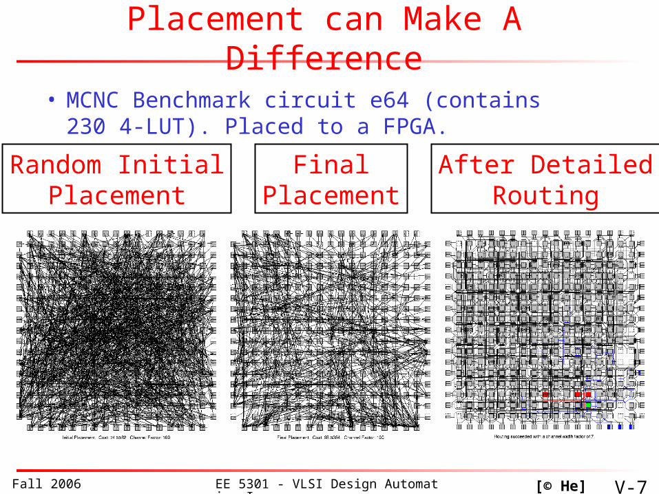
Placement can Make A Difference
• MCNC Benchmark circuit e64 (contains 230 4-LUT). Placed to a FPGA.
Random InitialPlacement
FinalPlacement
After DetailedRouting
[© He]

Fall 2006 EE 5301 - VLSI Design Automation I V-8
Design Types
• ASICs Lots of fixed I/Os, few macros, millions of standard cells Placement densities : 40-80% (IBM) Flat and hierarchical designs
• SoCs Many more macro blocks, cores Datapaths + control logic Can have very low placement densities : < 20%
• Micro-Processor (P) Random Logic Macros(RLM) Hierarchical partitions are placement instances (5-30K) High placement densities : 80%-98% (low whitespace) Many fixed I/Os, relatively few standard cells Recall “Partitioning w Terminals” DAC`99, ISPD `99,
ASPDAC`00
[© He]
Fall 2006 EE 5301 - VLSI Design Automation I V-9
Requirements for Placers
• Must handle 4-10M cells, 1000s macros 64 bits + near-linear asymptotic complexity Scalable/compact design database (OpenAccess)
• Accept fixed ports/pads/pins + fixed cells• Place macros, esp. with var. aspect ratios
Non-trivial heights and widths(e.g., height=2rows)
• Honor targets and limits for net length• Respect floorplan constraints• Handle a wide range of placement densities
(from <25% to 100% occupied), ICCAD `02
[© He]
Fall 2006 EE 5301 - VLSI Design Automation I V-10
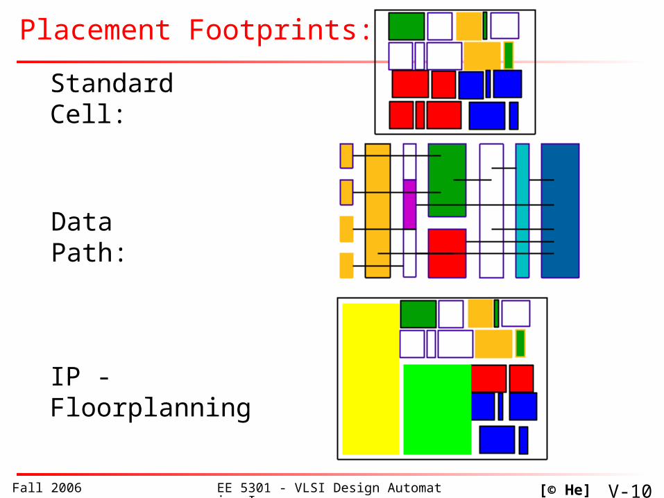
Placement Footprints:
Standard Cell:
Data Path:
IP - Floorplanning
[© He]

Fall 2006 EE 5301 - VLSI Design Automation I V-11
Core
ControlIO
Reserved areas
Mixed Data Path & sea of gates:
Placement Footprints:
[© He]
Fall 2006 EE 5301 - VLSI Design Automation I V-12
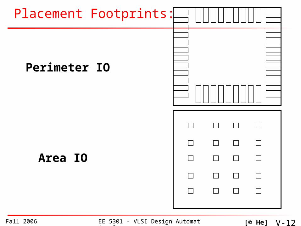
Perimeter IO
Area IO
Placement Footprints:
[© He]
Fall 2006 EE 5301 - VLSI Design Automation I V-13
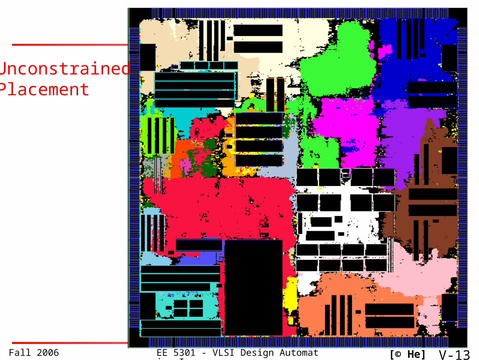
UnconstrainedPlacement
[© He]

Fall 2006 EE 5301 - VLSI Design Automation I V-14
Floor plannedPlacement
[© He]

Fall 2006 EE 5301 - VLSI Design Automation I V-15
VLSI Global Placement Examples
bad placement
good placement
[© He]
Fall 2006 EE 5301 - VLSI Design Automation I V-16
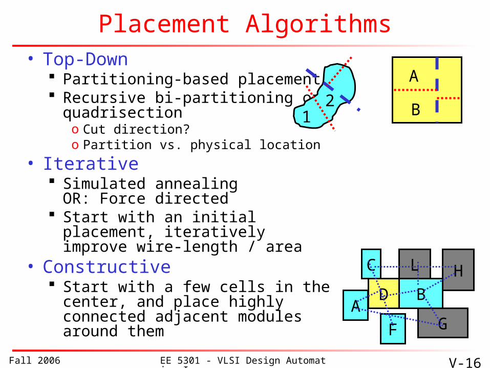
Placement Algorithms• Top-Down
Partitioning-based placement Recursive bi-partitioning or
quadrisectiono Cut direction?o Partition vs. physical location
• Iterative Simulated annealing
OR: Force directed Start with an initial placement,
iteratively improve wire-length / area
• Constructive Start with a few cells in the
center, and place highly connected adjacent modules around them
12 B
A
D B
FA
C
G
L H

Fall 2006 EE 5301 - VLSI Design Automation I V-17
Simulated Annealing Placement
• Cost Area (usually fixed # of rows, variable row width) Wirelength (Euclidian or Manhattan) Cell overlap (penalty increases with
temperature)
• Moves Exchange two cells within a radius R
(R temperature dependent?) Displace a cell within a row Flip a cell horizontally
• Low vs. High temperature If used as a post processing, start with low-temp
• Post-processing? Might be needed if there are still overlaps

Fall 2006 EE 5301 - VLSI Design Automation I V-18
Case Study: TimberWolf• “The Timberwolf Placement and Routing Package”, Sechen, Sangiovanni;
IEEE Journal of Solid-State Circuits, vol SC-20, No. 2(1985) 510-522• “Timber wolf 3.2: A New Standard Cell Placement and Global Routing
Package” Sechen, Sangiovanni, 23rd DAC, 1986, 432-439
Timber wolf
Stage 1 Modules are moved between different rows as well as within the
same row modules overlaps are allowed when the temperature is reduced below a certain value, stage 2
begins
Stage 2 Remove overlaps Annealing process continues, but only interchanges adjacent
modules within the same row
[© He]
Fall 2006 EE 5301 - VLSI Design Automation I V-19
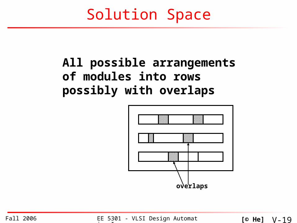
Solution Space
All possible arrangements of modules into rows possibly with overlaps
overlaps
[© He]
Fall 2006 EE 5301 - VLSI Design Automation I V-20
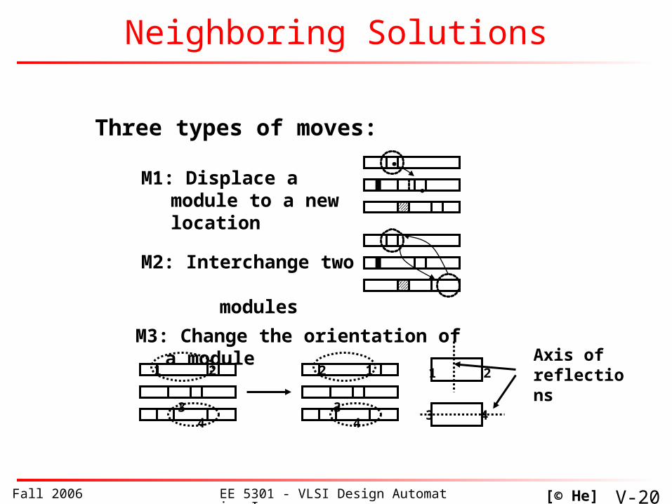
Neighboring Solutions
M3: Change the orientation of a module1 2
3 4
2 1
3 4
1 2
3 4
Axis of reflections
M1: Displace a module to a new location
M2: Interchange two modules
..
Three types of moves:
[© He]

Fall 2006 EE 5301 - VLSI Design Automation I V-21
Move Selection
• Timber wolf first try to select a move betwee M1 and M2
o Prob(M1)=4/5o Prob(M2)=1/5
• If a move of type M1 is chosen (for certain module) and it is rejected, then a move of type M3 (for the same module) will be chosen with probability 1/10
• Restriction on:• How far a module can be displaced• What pairs of modules can be interchanged
M1: Displacement
M2: Interchange
M3: Reflection
[© He]
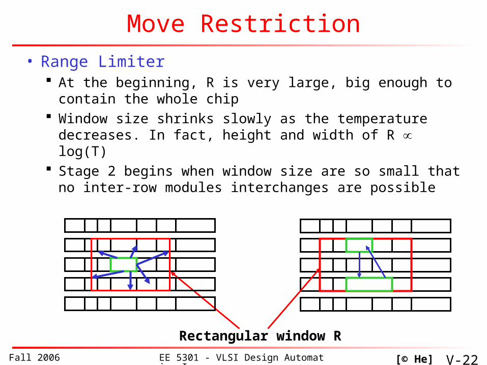
Fall 2006 EE 5301 - VLSI Design Automation I V-22
Move Restriction
• Range Limiter At the beginning, R is very large, big enough to
contain the whole chip Window size shrinks slowly as the temperature
decreases. In fact, height and width of R log(T) Stage 2 begins when window size are so small that
no inter-row modules interchanges are possible
Rectangular window R
[© He]

Fall 2006 EE 5301 - VLSI Design Automation I V-23
Cost Function
• Cost = C1+C2+C3
C1 = (aiwi + bihi)
ai, bi are horizontal and vertical weights, respectively
ai =1, bi =1 1/2 perimeter of bounding box
Critical nets: Increase both ai and bi
Double metal technology: Over-the-cell routing is possible. Fewer feed through cells are needed
vertical wirings are “cheaper” than horizontal wirings . use smaller vertical weights i.e. bi< ai
net i
hi
wi
[© He]

Fall 2006 EE 5301 - VLSI Design Automation I V-24
Cost Function (Cont’d)
C2: Penalty function for module overlaps
O(i,j) = amount of overlaps in the X-dimension between modules i and j
— offset parameter to ensure C2 0 when T 0
ji
jiOC2
2 ),(
C3: Penalty function that controls the row lengths
Desired row length = d( r )
l( r ) = sum of the widths of the modules in row r
r
rdrlC )()(3
[© He]

Fall 2006 EE 5301 - VLSI Design Automation I V-25
Annealing Schedule
Tk = r(k)•Tk-1 k= 1, 2, 3, …. r(k) increase from 0.8 to max value 0.94 and
then decrease to 0.1 At each temperature, a total number of K•n
attempts is made n= number of modules K= user specified constant
[© He]
Fall 2006 EE 5301 - VLSI Design Automation I V-26
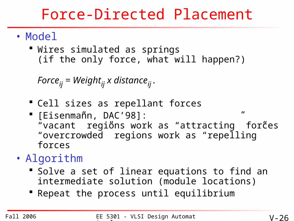
Force-Directed Placement
• Model Wires simulated as springs
(if the only force, what will happen?)
Forceij = Weightij x distanceij.
Cell sizes as repellant forces [Eisenmann, DAC’98]:
“vacant” regions work as “attracting” forces“overcrowded” regions work as “repelling” forces
• Algorithm Solve a set of linear equations to find an
intermediate solution (module locations) Repeat the process until equilibrium
Fall 2006 EE 5301 - VLSI Design Automation I V-27
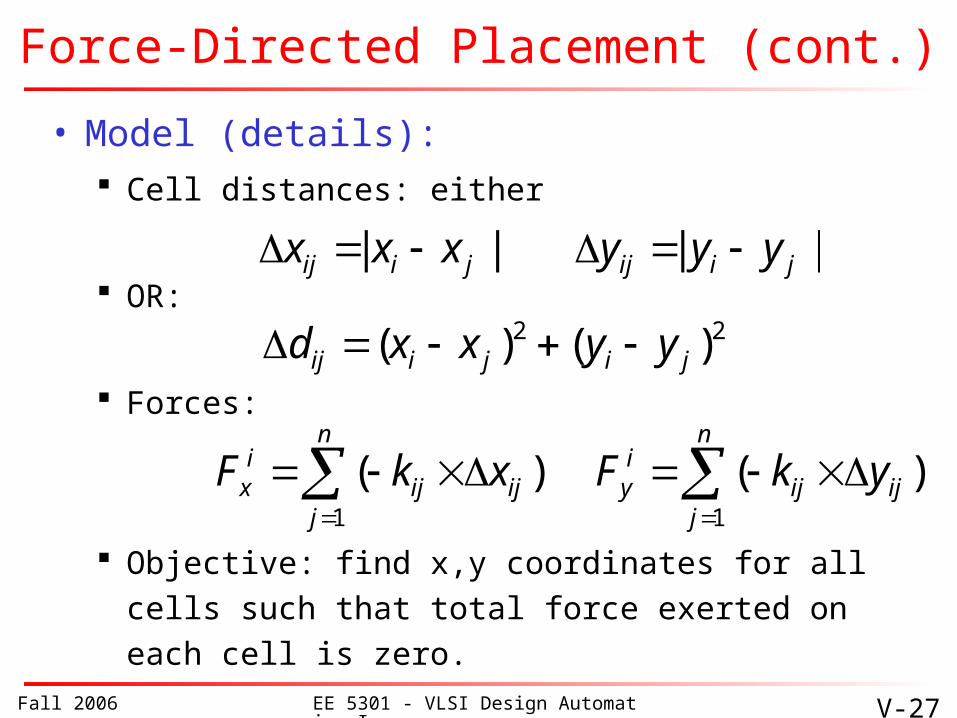
Force-Directed Placement (cont.)
• Model (details): Cell distances: either
OR:
Forces:
Objective: find x,y coordinates for all cells such that total force exerted on each cell is zero.
|||| jiijjiij yyyxxx
22 )()( jijiij yyxxd
)()(11
ij
n
jij
iyij
n
jij
ix ykFxkF

Fall 2006 EE 5301 - VLSI Design Automation I V-28
Force-Directed Placement (cont.)• Avoiding overlaps or collapsing in one point?
Use fixed boundary I/O cells Use repelling force between cells that are not
connected by a net Do not allow a move that results in overlap Use repelling “field” forces from congested areas
to sparse ones [Eisenmann, DAC’98]
• Problems with force directed: Overlap still might occur (cell sizes model
artificially) Flat design, not hierarchy
),()(1
iixij
n
jij
ix yxExkF

Fall 2006 EE 5301 - VLSI Design Automation I V-29
Partitioning-based Placement• Simultaneously perform:
Circuit partitioning Chip area partitioning Assign circuit partitions to chip slots
• Problem: Circuit partitioning unaware of the physical
location
Solution: Terminal propagation (add dummy terminals)
A B
A
B
A B
[She99] p.239
A B

Fall 2006 EE 5301 - VLSI Design Automation I V-30
Partitioning-based Placement• More problems:
Direction of the cut? [Yildiz, DAC’01]
How to handle fixed blocks? (area assigned to a partition might not be enough)
How to correct a bad decision made at a higher level?
• Advantages: Hierarchical, scalable Inherently apt for congestion minimization, easily
extendable to timing optimization
1
2 34 5
6 7
12 3
4 5
1234
56789
(a) (b) (c)
1 2
3
(d)
Fall 2006 EE 5301 - VLSI Design Automation I V-31
To Probe Further...• W. C. Elmore, “The transient analysis of damped linear networks with
particular regard to wideband amplifiers“, Jour. of Applied Physics, vol. 19, no. 1, pp. 55-63, 1948.(interconnect delay modeling)
• Hans Eisenmann and Frank M. Johannes“Generic Global Placement and Floorplanning”,Design Automation Conference (DAC), pp. 269-274, 1998.(force directed method)
• Maogang Wang, Xiaojian Yang and Majid Sarrafzadeh“Dragon2000: Standard-Cell Placement Tool for Large Industry Circuits”,International Conference on Computer-Aided Design (ICCAD), pp. 260-263, 2000. (partitioning-based placement)
• Dennis J.-H. Huang and Andrew B. Kahng“Partitioning-based Standard-cell Global Placement With An Exact Objective”,International Symposium on Physical Design (ISPD), pp. 18-25, 1997.(quadrisection-based placement)
Fall 2006 EE 5301 - VLSI Design Automation I V-32
To Probe Further...• Xiaojian Yang, Elaheh Bozorgzadeh and Majid Sarrafzadeh,
“Wirelength Estimation based on Rent Exponents of Partitioning and Placement”,System Level Interconnect Prediction (SLIP), pp. 25-31, 2001.
• A. R. Agnihotri, S. Ono, C. Li, M. C. Yildiz, A. Khatkhate, C.-K. Koh, and P. H. Madden,"Mixed Block Placement via Fractional Cut Recursive Bisection”,IEEE Trans. on Computer-Aided Design, Vol 24, No. 5, pages 748-761, May 2005.(partitioning-based placement)
• Chandra Mulpuri and Scott Hauck“Runtime and Quality Tradeoffs in FPGA Placement and Routing”,International Symposium on Field Programmable Gate Arrays (FPGA), pp. 29-36, 2001.(placement and routing quality/speed trade-off)