fabulous final report - cordis...over-silicon optical amplifier that was realized in the project....
TRANSCRIPT

PROJECT FINAL REPORT
Grant Agreement number: 318704
Project acronym: FABULOUS
Project title: FDMA Access By Using LOw-cost optical network Units in Silicon photonics
Funding Scheme: Collaborative Project
Period covered: from 1/10/2012 to 30/06/2016
Name of the scientific representative of the project's co-ordinator1, Title and Organisation:
Ing. Silvio Abrate, Head of Applied Photonics, Istituto Superiore Mario Boella
Tel: +39 011 2276302
Fax: +39 011 2276299
E-mail: [email protected]
Project website address: http://www.fabulous-project.eu
1 Usually the contact person of the coordinator as specified in Art. 8.1. of the Grant Agreement.
2
1.1 Final publishable summary report
1.1.1 Executive summary The FABULOUS project has developed a Passive Optical Network (PON) system, based on a reflective approach, that is compatible with legacy infrastructures, or at least with standardized PON infrastructures, while being capable of granting a threefold capacity increase with respect to the most advanced PON standard (ITU-T G.989, usually referred to as NG-PON2) existing so far; peculiarity of this system is having been conceived in order to allow massive optical integration of the customer premises equipment, the so called Optical Network Unit (ONU), onto silicon, in order realize optical modems with consumer electronics target prices, fore really envisioning fiber in every apartment and not only for high-end customers or clusters of customers (such as Fiber-To-The-Curb or Fiber-To-The-Building approaches). More in detail, from a scientific point of view FABULOUS has demonstrated that:
a Reflective PON, characterized by very challenging transmission performances to be achieved, mostly from the point of view of the power budget, can respect the same Optical Distribution Network (ODN) targets set by current PON standards and infrastructure, provided that powerful Digital Signal Processing (DSP) can be adopted together with coherent detection at the central office (the so called Optical Line Terminal – OLT). The reflective PON approach has several well-known advantages with respect to a traditional PON, as it avoids having lasers at the customer equipment lowering its cost, improving eye-safety and simplifying the control layer of the network as all optical sources are then in the central office only;
Frequency Division Multiplexing (FDM) can be a very effective technique in high-speed PONs as it allows the users’ equipment to run at low-speed and enables long error correction and equalization schemes, while on the contrary Time Division Multiplexing (TDM) requires the users’ equipment to be able to run at the full network speed, rather than at the single user’s speed, and does not allow powerful DSP techniques to be employed;
it is possible to realize highly integrated ONUs by means of Photonic Integrated Circuits (PIC) on silicon platform, with a level of maturity close to commercialization. In particular, we realized a PIC including a 2D grating coupler, a polarizing beam splitter and a Mach-Zehnder modulator with segmented electrodes on a silicon chip, and properly multi-stage electrical driver on 65nm CMOS technology flip-chipped on top of the silicon device. Such device was demonstrated to work in the full system, however not yet achieving the same performances of semiconductor discrete components;
as on-chip amplification is needed to broaden the fields of application of silicon photonics, hybrid integration of InP-based material on silicon provides a promising path, as demonstrated by the InP-over-silicon optical amplifier that was realized in the project. Integration of such amplifier in a more complex integrated device still has to be perfected.
In addition to the scientific outcomes mentioned above, that are now setting the state-of-the-art for photonic integration and reflective passive networks as testified by the huge number of scientific journals published by the project partners, we also learned other important lessons: first of all, co-design of system and devices is a key for exploiting the full potential of silicon photonics; secondly, once the potential market of the relevant silicon devices will reach millions pieces per year, as hopefully should be in the short term for PON since already millions subscribers of older PON services currently exist mostly in Asia, then most of the cost will be due to the packaging, and thus some techniques for lowering packaging cost should be sought in the next few years.

3
1.1.2 Project context and objectives Fiber-To-The-Home is widely accepted to be most future-proof approach for delivering broadband to a majority of the population, since once the fiber infrastructure will be reasonably deployed then just a modification of the central office (CO) and/or of the customer premises equipment (CPE) will be able to grant speed or service improvement for decades, while the same does not hold true for copper-based or wireless infrastructures. In this context, passive optical networks (PON) are the network architectures accepted by operators, equipment vendors and researchers as the solution to be pursued, in particular in its power-splitter based approach (point-to-multipoint networks where only power splitters are present in the distribution networks, to be compared with approaches in which wavelengths separation is rigidly performed in the networks), to the point that already millions subscribers to different generations of PON service (EPON, GPON and XG-PON) exist mostly in Japan and South Corea. For increasing the service coverage, next PON solutions will have to face some major challenges, in particular:
in terms of infrastructure: compatibility with legacy networks, as the investments operators make on fiber installations should last for at least 20 years;
in terms of system: capability of granting high performances in terms of splitting-ration (number of users reached by a single PON tree) and speed (per user and aggregate), while finding low-cost solutions able to allow at least the ONU to reach consumer electronics target prices.
Recently, ITU-T with input from the FSAN (Full Service Access Network) initiative, has released a new PON standard dubbed G.9892, and usually referred to as NG-PON2 (Next Generation PON v2), that is then setting the state-of-the-art for new equipment, with the following main characteristics:
Time-Division-Multiplexing (TDM) is adopted for allowing multiple users per wavelength: every user is assigned a time slot during which it is connected to the OLT;
the system should allow up to 4 wavelengths; on every wavelength, max speed of 2,5 Gbps in US and 10 Gbps is DS must be granted: this means that, when connected to the OLT, every ONU must be capable of affording such speeds;
peer-to-peer services, with dedicated wavelength, can be offered to major customers.
Some open issues for the realization of proper G.989 equipment still exist, and coupled to some technological compromises accepted in setting the standard, we believe it will be hard to see low cost CPE in a reasonable term; for example:
a) as 4 wavelengths are foreseen by G.989, and co-existence on the same infrastructure with a number of older services (i.e. CATV) it has been decided needs to be allowed, the CPE will need to use tunable lasers capable of operating on a 100 GHz grid, and no low-cost solution currently exists for this problem;
b) as ONUs could in principle switch -on and -off upon users will, some control layer needs to be implemented in order to avoid that, at the time of the switch-on, uncontrolled wavelengths blind the Optical Line Terminal (OLT) in the CO, blocking the network, since the wavelength a tunable laser is working at when just switched-on is unknown;
2 G.989.1 40-Gigabit-capable passive optical networks (NG-PON2): General requirements

4
c) the TDM approach, as previously mentioned, requires every user to be capable, in its operational time slot, to be able to run at the full network speed, that is times faster than its average speed (i.e. in a PON with 32 users to the same PON service, the average speed per user is 1/32 of the full speed). This situation creates a sort of “low” (with respect to other multiplexing approaches) cap to the network speed, and requires the CPE to be over-dimensioned, and thus too expensive, with respect to the real traffic generated/received.
The FABULOUS project tries to answer to those and other challenges, providing a credible alternative to G.989 and its evolutions, studying architectural and technological solutions to answer to both low-cost and high-performance requirements, based on the following main pillars:
instead of a conventional PON that uses one laser for downstream at each OLT in the central office for downstream (DS) traffic and one laser for every ONU for upstream (US) traffic (yielding for example 33 lasers in a single PON with 32 users), FABULOUS is based on a reflective PON, having no laser at the ONU and inserting an additional source at the OLT that is sent unmodulated through the Optical Distribution Network and used as seed by every ONU for the US direction. This approach allows to totally solve issues a) and b), and contributes to lower the cost of the solution as the number of lasers is decreased (2 lasers per PON regardless the number of users) and the complexity of Wavelenght Division Multiplexing (WDM) is mostly left at the OLT, while the ONU will only need a tunable filter. This approach has the drawback of a challenging US power budged, as the seed experiences twice the ODN loss, then a self-coherent detection, using the seed as Local Oscillator (LO) as well, is employed at the OLT;
Frequency Division Multiplexing is used instead of TDM to multiplex, at the electrical level, the different users of every wavelength. With this approach, every ONU is constantly communicating with the OLT rather than only in the dedicated time slot, so that the ONU needs to work at its baud-rate only and not at full network speed. Another advantage of the constant connection between OLT and ONU is the possibility to mike wide adoption of Digital Signal Processing (DSP) for improving the transmission performances, such as powerful Forward Error Correction (FEC) and equalizers, and easily allowing multilevel modulation formats;
the optical part of the ONU has been conceived in order to be fully integrated on Silicon Photonics (SiP), a very promising technology for allowing consumer electronics prices when mass-market volumes are achieved. All the needed functions (modulation, optical filtering, electrical driving, amplification) can be realized in a Photonic Integrated Circuit (PIC) with dimensions of a few square millimeters and in millions pieces per year with already available facilities. In the FABULOUS project, the functionalities of this ONU are in a first phase demonstrated with discrete components when the PIC is being realized, and then demonstrated with the PIC itself in a second phase.
For accomplishing to such ambitious tasks, a consortium formed by research institutions, universities, telecom operators and large companies has been formed, involving competences of optical systems, SiP devices realization, packaging. The full consortium is detailed in the following table.
No. Participant organisation name Short name Country
1 (Coordinator)
Istituto Superiore Mario Boella ISMB IT
2 Politecnico di Torino POLITO IT
3 Commissariat a l’energie atomique et aux energies
alternative CEA-LETI FR

5
4 Orange SA ORANGE FR
5 STMicroelectronics SRL ST-I IT
6 Tyndall National Institute, University College Cork TYNDALL-UCC IE
7 Università degli studi di Pavia UNIPV IT
8 III-V Lab III-VLAB FR
In summary, the main technical objectives of FABULOUS are:
1. the demonstration of a self-coherent reflective PON based on Frequency Division Multiplexing at the electrical level and Wavelength Division Multiplexing at the optical level, targeting the symmetric transmission of 1 Gbps to at least 32 users per wavelength, considering an Optical Distribution Network compatible to the one described in the XG-PON standard (inherited by G.989);
2. the realization of the ONU realizing the functions needed by the above mentioned PON in the form of a Photonic Integrated Circuit based on Silicon Photonics, performing optical filtering, modulation and, if needed, optical amplification, as a proof of the fact that silicon will allow optical devices to become suitable for consumer electronics.
The project started on the 1st of October 2012, and lasted 45 months including a 9-months extension due to a fire accident that damaged the clean-rooms of partner CEA-Leti, where the ONU PIC was being realized.
1.1.3 Main S&T results/foregrounds FABULOUS has been organized in 5 work-packages, but besides describing the activities realized in every WP, in the following we will describe a logical sequence of results and achievements, even if many of them are the outcomes of activities running in parallel or related to the same WP. In particular, the results are summarized in the following main groups:
1. Realization of the FABULOUS architecture with discrete components, for realizing the needed DSP and assessing the maximum achievable performances with the off-line processing approach. Evaluation of the feasibility of the DSP in real-time.
2. Step-by-step realization of the ONU in the form of PIC, first by realizing the different building blocks and then the full integrated device on Silicon Photonics.
3. Insertion of the ONU PIC in the full network, replacing the discrete ONU.
Benchmarking with discrete components
As the FABULOUS ONU PIC would have come available only towards the end of the project, we started evaluating the performances of the architecture with commercial discrete components; this phase was also fundamental for starting from the very beginning of the activities the study and realization of the DSP needed to maximize the performances, in order to make only small adjustments tailored on the PIC once available. The architectural principle previously mentioned is recalled in Fig. 1. Both the reflective approach and the possibility to multiplex in frequency at the electrical level are known in literature even if never adopted for standardized equipment.

6
Figure 1: reflective PON based on Wavelength Division Multiplexing at the optical level and Frequency Division Multiplexing / Multiple Access at the electrical level. One of the FABULOUS novelties resides in the way the reflective PON is realized, very different to the conventional approaches based of Reflective Semiconductor Optical Amplifiers (RSOA) or Reflective Electro-Absorption Modulators (REAM), and resumed in Fig. 2 and Fig. 3.
Figure 2: splitting of DS traffic and US seed, and modulation with US traffic.
Figure 3: detail on the upstream section of the FABULOUS ONU.
The ONU performs the obvious action of separating the US seed from the DS wavelengths, then photodetecting the DS traffic, and this is basically done by means of an optical filter and a photodiode. For the US part, the ONU works as follows (Fig. 3):
a Polarizing Beam Splitter (PBS) separates x and y polarization of the seed and sends them in the opposite directions of the ONU loop;
optical amplification and wavelength filtering are made by means of SOAs and tunable filters, to meet the power budget needs and provide wavelength tunability;
modulation in made through a Mach-Zehender Modulator (MZM) with the two independent electrodes fed by the same modulating signal, eventually applied to a properly realized driver. When the two MZM branches are perfectly symmetrical and the MZM electrodes work in travelling wave mode, the device turns out to be independent on the input polarization and implements a 90° polarization rotation in reflection, and such polarization rotation is preserved along the whole US path, thus allowing a simplified single polarization homodyne coherent detection at the OLT (Fig. 4);
the whole ONU in Fig. 3, apart from the input polarizing beam splitter, requires internally handling only one polarization, which can be made coincident with the TE-mode of the used waveguides. This

7
requires careful polarization management and massive use of polarization maintaining (PM) fibers when realizing the circuit with discrete components, but turns out to be is a key advantage for the PIC as it is intrinsic in SiP platforms.
Figure 4: simplified self-coherent detection at the OLT. The ECL laser provides seed sent to the ONU to be used for US traffic and the local oscillator for the coherent receiver. Thanks to the 90° polarization rotation, one of the two branches of the coherent receiver is always null. It is evident that most of the innovation in state-of-the-art provided by FABULOUS resides in the upstream direction, as the DS is a quite conventional FDM transmission over fiber; in the following then, we will then focus on the US while providing only quick comments and results about the DS. As previously mentioned, at first the ONU has been implemented with discrete optical components, emulating as much as possible the integrated circuit; due to polarization requirements, as after the PBS single polarization has to be guaranteed, instead of two SOAs put “in the loop”, we decided to utilize one single SOA before the PBS, and the polarization maintaining (PM) fibers after the PBS to close the loop on the modulator; the MZM itself is actually not a very common unit, as for our setup we need to have independent access to both electrodes, driven with the same electrical signal, as commercial devices now usually have one only access. The two electrodes, eventually through electrical drivers, are connected to an Arbitrary Waveform Generator (AWG) or a Field Programmable Gate Array (FPGA) by means of an electrical splitter. The most comprehensive set of experiments was performed with an ODN composed by a dark fiber of about 40 Km going through the city of Turin and a variable optical attenuator (VOA) for spanning different values of ODN loss, as specifications require those 40 Km as minimum distance and a loss value to accommodate different qualities of the installation rather than different passive splitting ratios; we assembled a total of 5 working ONUs for creating all the possible electrical interferences, and then we added the noise of other 27 ONUs by means of a noise loading mechanism, so to emulate the full noise that a test channel can be subject to when the full network is working. It is worth mentioning that the above described situation is a sort of worst-case scenario, in which all the users are subject to the same attenuation condition, that is in the end the maximum requested by the standard, however this is not a real case in which customers experience different link conditions, and a statistical analysis of this situation will be reported afterwards.

8
Figure 5: Scheme of the optical part of the US section of the ONU realized with discrete components.
Figure 6: laboratory setup for the ONU with discrete optical components.
Much research was done on the electrical side, first with the off-line processing approach, generating the transmitted stream with an AWG and then receiving it with a Real-Time Oscilloscope (RTO) for processing it with Matlab™ in a first phase, using an FPGA for real-time Ethernet transmission in a second phase. In particular, after a long campaign of simulation and experiments, the final electrical signal feeding the FABULOUS architecture was treated as follows:
on every electrical subcarrier, we used spectrally efficient modulation formats. Most of the experiment were carried out with 16-QAM as the best compromise between performances, complexity and bandwidth requirement. The signal was shaped with a square-root-raised-cosine (SRRC) with a roll-off factor of 0,1;
Forward Error Correction (FEC) is foreseen. Powerful FEC with an overhead of about 20% allow pre-FEC Bit Error Rates (BER) in the order of 10-2, granting great power budget increase.
considering an initial target of 1 Gbps per user, the two previous points yield an electrical bandwidth of around 330 MHz per user, and considering 32 users per wavelength an optical modulator with an electrical bandwidth of about 10 GHz is needed;
optimized band-plan for the electrical subcarrier in terms of both frequency spacing and absolute positioning of the FDM electrical comb. In particular, no frequency guard-band is foreseen between channels, and a proper allocation for making second-harmonics fall in the middle of two adjacent channels is employed;
second and third harmonic nonlinearity in the R-MZM, which are proportional to the electrical signal amplitude over the R-MZM electrodes, have been studied and minimized. Defining the modulation index mindex as the ratio between the modulated electrical peak voltage (i.e. the amplitude of the RF M-QAM electrical signal) and the modulator Vπ, we performed an extensive analysis to optimize it in terms of maximum reachable ODN loss. Under our target upstream transmission conditions (~30 dB of ODN loss), the modulation index must be in the range 0.15 mindex 0.25. This optimal range finds a balance between two counteracting effects: for increasing modulation indices, the useful modulated optical signal increases (which is advantageous at the OLT receiver), but also the second and third harmonic components grow, generating detrimental interference with other subcarrier. On

9
the contrary, for low modulation indices the nonlinearities are negligible but at the same time the useful signal is smaller;
at the OLT, two coherent receiver electrical outputs are subject to a down-converting stage, reducing the DSP rate to 2 sample/symbol (≈600 MSample/s), a feed-forward adaptive equalizer, with 31 complex taps updated by Constant Modulus Algorithm (CMA), a Carrier Phase Estimation (CPE) using a Viterbi-Viterbi algorithm.
Figure 7: effect of channel spacing. Worsening of performances when spacing between central frequencies is lower than 90% the baud rate (330 Mhz).
Figure 8: effect of modulator non-linearity related to the modulation index. 16-QAM optical spectrum at the output of a single ONU, for subcarrier frequency equal to 2 GHz, mindex = 0.2 or 0.4. The frequency axis is set so that f=0 corresponds to the CW laser central frequency.
One of the key optimization procedures we implemented was related to the SOA working conditions, as highlighted by Errore. L'origine riferimento non è stata trovata.that shows the resulting BER vs. SOA bias current for two different modulation indexes and a fixed 25 dB ODN loss. From this figure, it is possible to notice how a wrong choice on the SOA bias current can cause a significant penalty on the system performances. In fact, if the bias current is too low, a low signal-to-noise ratio is obtained at the receiver; on the contrary, if the bias current is too high, the SOA works in its saturation region and the received signal results distorted. Therefore, for every working condition identified by the pair of parameters mindex and ODN loss, the optimum SOA bias current has been computed and collected
Figure 9: Pre-FEC BER vs. SOA bias current, for a mindex of 0.2 and 0.4 and ODN loss of 25 dB.
Figure 10: Optimum SOA bias current for each working condition (mindex and ODN loss).
75
100
100
125
125
125
150
150
150
150
175175
175
175
200
200
225
225
250
ODNLOSS [dB]
Mod
ulat
ion
Inde
x [%
]
20 21 22 23 24 25 26 27 28 29 3010
15
20
25
30
35
40
SOAbias
2
3
10
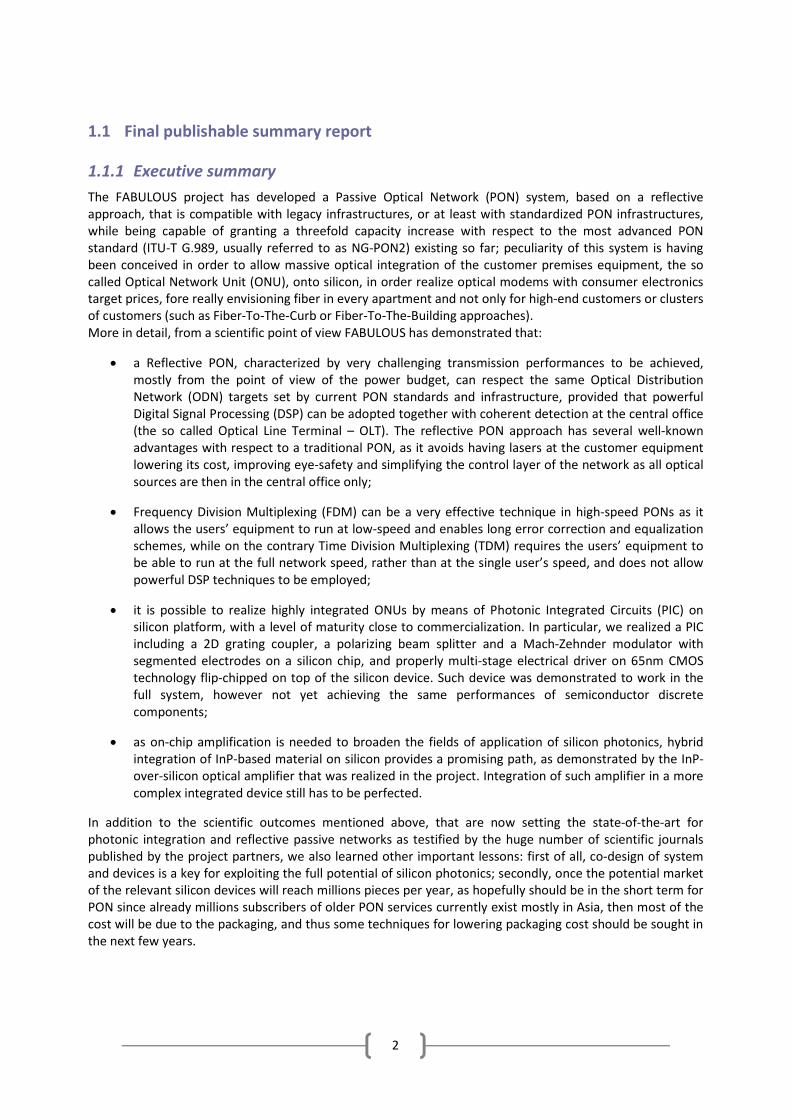
This very wide experimental phase led us to demonstrate, with the off-line processing approach, the most important system result of the whole project, a real proof-of-concept of a self-coherent reflective PON capable of transmitting 1 Gbps to 32 users (for an aggregate capacity per wavelength of 32 Gbps) with an ODN loss greater than 31 dB3; this result is very important as 31 dB is one of the most common ODN loss classes standardized by ITU-T, referred to as Class N2, while sticking with a launched power of +9 dBm. The FDM/FDMA PON concept allows the capacity to be reattributed dynamically to respond to the customer demand which understandably varies over time depending on the services requested, hours of day and night, etc… Indeed, when a customer requests a transmission capacity (e.g. in order to download a film from his remote data storage), the system will identify an available frequency channel from the 32 possible channels and associate that frequency channel to that customer for the duration of the data exchange. During that time, the transmission is performed at the maximum available speed until completion in order to free the frequency channel for another request or another customer. As already mentioned, in our experiment, we emulated a worst case situation in which all ONUs see the worst case ODN loss. Anyway, on realistic PONs, users typically see different losses4, so the quality of the transmission channel is dependent upon the physical parameters of the user requesting capacity. As the (de)modulation is performed in DSP, it is possible to implement various levels of QAM modulation coding (from e.g. QPSK to 128-QAM) which will lead to different transmission capacity per RF channel. For instance, we can range from 500 Mbps in QPSK to 1.75 Gbps in 128-QAM over the same electrical bandwidth we used in the previous experiment to deliver 16-QAM at 1 Gbps, while other values can be obtained also varying the electrical bandwidth per channel. For each transmission to a specific user, the QAM modulation level can be adapted to achieve the maximum transmission speed and hence the minimum time occupation of that channel. The traffic towards (or from) different users sharing the same RF channel can be, for instance, multiplexed also in the time domain. Using a proper model to infer the performance of the FDM/FDMA PON over a broader range of user losses, we showed for instance that a standard class N2 PON with an average user loss of 21.4 dB should be able to transport 48 Gbps in US (64-QAM for each user) and 56 Gbps in the DS (128-QAM per user). Sticking back to the experimental validation, we then assessed the performances of the FABULOUS architecture varying modulation format and electrical bandwidth, still using the same setup and optical parameters (link length, launch power, etc.). It is important to point out that no hardware modification was necessary to make these adaptations, that only requested intervention on the DSP and on the electrical signal generation (to be performed on FPGA or ASIC platform in a final version). The following table reports the results of these experiments, where we assumed that every user employs the same electrical bandwidth. In a more general case in which every user could also adopt a different bandwidth, that is a possibility foreseen by FDM approaches, such values provide only a rough estimation, since in that case the interference at the electrical level can be quite variable depending on the overall spectrum shape. As an approximate indication, we estimated that, a user experiencing for example an attenuation greater than 40 dB can still be connected to the network at 250 Mbps using BPSK modulation with a bandwidth of 330 MHz or at 100 Mbps using QPSK modulation with a bandwidth of 66 MHz. On the contrary, users experiencing a lower attenuation can increase their bit-rate; for instance, in case all users are below 23 dB of attenuation, the network could grant an aggregate bit-rate close to 50 Gbps using 64-QAM. Full results are reported in the following table:
3 “Optimization of Reflective FDMA-PON Architecture to Achieve 32 Gb/s Per Upstream Wavelength Over 31 dB ODN Loss”, Journal of Lightwave Technology Vol. 33 Issue 2. 4 “Versatile customers, do we have FTTH solutions?”, in Proc. European Conference on Optical Communication, Cannes, France, Sep. 21-25, 2014, Paper TH261.

11
Modulation format
Electrical bandwidth per channel Net bit-rate per user Maximum ODN
loss 64-QAM 660 MHz 3 Gbps 23.0 dB 64-QAM 1320 MHz 6 Gbps 23.0 dB 16-QAM 330 MHz 1 Gbps 31.0 dB 16-QAM 1650 MHz 5 Gbps 30.5 dB 16-QAM 3300 MHz 10 Gbps 28.0 dB
QPSK 66 MHz 100 Mbps 41.0 dB QPSK 330 MHz 500 Mbps 38.0 dB QPSK 1650 MHz 2.5 Gbps 34.5 dB QPSK 3300 MHz 5 Gbps 32.5 dB BPSK 330 MHz 250 Mbps 40.5 dB OOK 6250 MHz 10 Gbps 38.5 dB
It is worth noting that, if every user requires 100 Mbps operation, then the resulting power budget is able to support the 40 Km of fiber and at least a 1:128 splitter (even 256, depending on the fiber attenuation the operators use to take into account for metropolitan installations); 256 users cannot be supported by our setup due to the electrical bandwidth of the LiNbO3 modulator we employed, however it is not difficult to find suitable ones on market. As a further comparison with NG-PON2, where super-users such as mobile operators would need a dedicated wavelength for front or back-hauling, we can observe that with these performances a user demanding great speed could coexist on the same wavelength with other users: in principle, the bandwidth we have considered for our experiments could allow for example one user using about 6 GHz to reach very high bit-rates, and leaving about additional 4 GHz for any type of the other users reported in the previous table (e.g. 63 additional users at 100 Mbps, yielding a total of 64 ONUs). We also like to mention that 64-QAM operation with 330 MHz is not possible due to phase-noise affecting the coherent detection, linked to the laser linewidth (< 100 KHz with the ECL unit used in this setup), and for the same reason we did not perform any campaign employing 128-QAM. When thinking of possible improvement in the FABULOUS architecture, it can be in general observed that employing a modulator with a greater bandwidth with respect to the custom unit we used could bring a twofold benefit: from one side, it could allow a bit-rate per user increase, from the other it could allow to use only the more robust modulation formats without decreasing the bit-rate but granting an increase in the power budget and thus in the possible splitting ratio, as can be seen in the following table obtained by numerical simulation using other modulator electrical bandwidths than the reference (11 GHz) used in the experiments. This upgrade would only involve the optical modulator: the FABULOUS architecture is then definitely scalable.
Modulator bandwidth
Number of ONUs per λ
Net Bit-rate per ONU and modulation format
Total upstream net Bit-rate per λ
Maximum ODN loss
11 GHz (reference) 32 1 Gbps (16-QAM) 32 Gbps 31.4 dB
22 GHz 32 2 Gbps (16-QAM) 64 Gbps 29.3 dB 22 GHz 32 2,5Gbps (32-QAM) 80 Gbps 25.1 dB 22 GHz 64 1 Gbps (16-QAM) 64 Gbps 30.1 dB 33 GHz 32 3 Gbps (16-QAM) 96 Gbps 28.1 dB 33 GHz 32 2.25 Gbps (8-QAM) 72 Gbps 32.0 dB 33 GHz 64 1,5Gbps (16-QAM) 96 Gbps 28.7 dB 33 GHz 64 1,1Gbps (8-QAM) 72 Gbps 33.0 dB
As the ONU is conceived to host optical tunable filters as well for WDM operation, we tested also a 4 wavelength scenario, that is the most evolved for G.989, and as expected no penalty on the ODN loss with

12
respect to the single wavelength case was found. We tested a high-capacity scenario, targeting 4 wavelengths at 32 Gbps each for a total of 128 Gbps, and the results are the following:
Number of ONUs Bit-rate per ONU Maximum ODN loss Theoretical splitter
insertion loss Optical margin
32 4 Gbps 27 dB 15 dB 12 dB 64 2 Gbps 28 dB 18 dB 10 dB
128 1 Gbps 31 dB (Class N2) 21 dB 10 dB A possible alternative is lowering the per-wavelength bit-rate to 10 Gbps, for a total of 40 Gbps, with then the same exact target performance of G.989, for a long-reach/high-splitting-ratio scenario, achieving the following performances:
Number of ONUs Bit-rate per ONU Maximum ODN loss Theoretical splitter
insertion loss Optical margin
128 375 Mbps 37 dB (Class E2) 21 dB 16 dB 256 187.5 Mbps 38 dB (Class E2) 24 dB 14 dB 512 93.75 Mbps 39 dB (Class E2) 27 dB 12 dB
The performances of a 4-wavelenght FABULOUS PON are summarized in the following figure envisioning a tree with two levels of splitting.
Figure 11: the FABULOUS PON with 4 wavelengths and two levels of splitting.
In the end, the FABULOUS system has proven to grant high-performance, be versatile and scalable; all these features are possible also because of the adoption of DSP, that as previously mentioned, is not easy to be implemented in TDM. It is then important to demonstrate as well the feasibility of the implementation of such DSP for real-time transmission and not in off-line only, so we proceeded to implement the full DSP on FPGA platforms, adjusting the software to consider the limitation such platforms have with respect to PCs (for example: finite math implementation instead of floating point, equalizer implemented as a 4:1 down-sampling filter, no real-time equalizer coefficients update, etc.); for what we consider to be the main experiment, that is the one using 16-QAM for reaching 1 Gbps per user, the ODN curves that we obtained in real-time were exactly the same obtained with the off-line processing with the only difference due to the fact that in rea-time we stopped to a pre-FEC BER of 10-4 as we employed a less powerful FEC not having at our resource the code of the better one.

13
Realizing a chip with the software was not in the scope of the project and anyway not in our possibilities, however we have been able to analyze the feasibility of an ASIC realization for replacing the FPGA (not to be used in commercial devices for consumer electronics). For performing this task, we obtained detailed information on DSP complexity from our experience on the FPGA-based real-time DSP demonstrator that we are currently developing inside the FABULOUS project.
Figure 12: the real-time operating ONU, with discrete optical components and FPGA boards.
Figure 13: the real-time operating ONU, with FPGA boards.
Focusing on the DS channel, for example purposes, the ONU receiver has to perform the following steps to convert the received optical signal to Ethernet data for the user: after the optoelectronic front end, the electrical signal is filtered and demodulated with an I/Q demodulator (to select the wanted FDMA channel). The two baseband I/Q components are sampled with a two channel A/D Converter (ADC) and enters the DSP domain, were the full FABULOUS physical layer and the Ethernet interface should be implemented. For mass production purposes, it is fundamental to include as many as these functionalities as possible in a single companion ASIC. In the following, we estimate the Silicon Area required for implementing the DSP, the Ethernet PHY and the converters. For the DS receiver section, the ONU chip should include:
a two channel 600 MHz Analog to Digital Converter (ADC);
an adaptive low-pass down-sampling filter, to reduce noise and interferences from adjacent subcarriers. After careful optimization simulation, this filter is implemented as a FIR filter with 32 complex taps;
the CPE, whose area is estimated on the bases of the off-line implementation;
a differential decoder;
a FEC decoder based on ITU G.975 I.4 EFEC, with area estimation based on FEC datasheets of the FPGA supplier.
For the US section, our analysis considered three main blocks:
a FEC encoder using a 20.5% overhead. Such code is composed by a Reed Solomon RS(781,765) outer code and a concatenated QC-LDPC code as inner code. The resulting area occupation of both FEC encoders is negligible with respect to DSP area occupation;
a SRRC up-sampling filter, made of 128 complex taps;
a dual 600 MSps Digital to Analog Converter (DAC).

14
It is worth pointing out that the complexity of the US FEC resides mostly at the OLT, for the FEC decoding phase, where computational complexity is less of an issue compared to the ONU side since the overall cost can be shared by all users. Considering a 65 nm process (optimized for power and for analog components) for the ASIC migration, our estimation leads to a more than reasonable 7 mm2 required area. Considering the size of the chip and a standard low-power 65 nm CMOS process, the static power consumption of such ASIC should be negligible; for what concerns dynamic power consumption, taking into account the operating speed of 300 MHz, a 1 V power supply and standard CMOS gate capacitance, it should be below 4.2 W. The FABULOUS DSP is then effective and realizable on ASIC for mass production.
Development of the integrated ONU
The target characteristics set by the FABULOUS system experts for the characteristics of the integrated ONU in order to achieve the same performances granted by discrete components is resumed in the following table:
R-MZM parameter Specification
Operational wavelength band 1550 nm Input PBS insertion loss 3 dB on both output ports
Input PBS polarization extinction ratio 30 dB should be sufficient Tunable optical filter operation band 1530 nm – 1570 nm Tunable optical filter channel spacing 100 GHz
Tunable optical filter bandwidth @ -20 dB < 100 GHz Tunable optical filter insertion loss < 1 dB
Tunable optical filter spectral uniformity of insertion loss < 1 dB Tunable optical filter suppression of adjacent channels > 30 dB
Tunable optical filter suppression of non-adjacent channels > 40 dB
Tunable optical filter in-band amplitude ripple < 0,5 dB SOA gain Selectable from 10 dB to 20 dB
SOA noise figure 3-7 dB MZM insertion loss < 5 dB
MZM electrical 3 dB bandwidth including drivers > 8 GHz
Electrical driver requirements At least 20% of MZM Vπ with total harmonic distortion better than 20 dB
Of course that has mostly to be considered as a wish list to drive the PIC development rather than a real specification achievable by a research project.
Figure 14: example of wafer-mapping with 22 sites for measurement

15
The full ONU PIC was not in the scope of the project, requiring too long development time, however demonstration of all the building blocks plus a preliminary ONU, as proof of the feasibility of the concept, has been achieved. The main blocks described in the following, prior to providing results about a partially integrated ONU, are the 2D grating coupler, the tunable filter, the modulator, the SOA and the electrical driver. Validation of the stand-alone building blocks is not straightforward, as test structures need to be put in place especially for the blocks to be realized on silicon (couplers, filters, modulators); some measurement have also been done on wafer (Fig. 14), also for validating the process integrity between the production steps. Overall performances are strictly connected to waveguide and process characteristics (guide size, etch depth, etc.), and in the following we will report only about the best results obtained without entering to much into process details. One of the project target was the design of a 2D grating coupler providing a total coupling-efficiency (CE) better than -4dB at 1550nm, while remaining compatible with the materials and fabrication process-flow of the project. In addition, the coupler should provide a 1 dB bandwidth of 30 nm and have input-polarization insensitivity comparable to established experimental values (-0.4dB). As the footprint of the 2D grating is negligible with respect to the overall device footprint, homogenous gratings (not focusing) were considered followed by a taper section. The main constraints to the coupler design are the fixed Silicon Oxide Insulator SOI-layer thickness of 220 nm and the bottom-oxide layer (BOX) thickness of 2000 nm. The top-oxide is assumed to fully fill the holes of the grating coupler.
Figure 15: (a) Schematic of light from a fibre source (with an angle-of-incidence of 10°) coupling into 2D-grating coupler. (b) and (c) The light is directed to the coupler region, through an index-matching layer, using total-internal-reflection from a polished fibre facet. The inset of shows the three variables (E = etch-depth, R = hole-radius, and P = grating-pitch) used to optimize the coupler response at 1550nm. The material cross-section, consisting of a top-oxide layer (TOX), a patterned silicon-on-oxide layer (SOI), the buried-oxide layer (BOX), and the silicon substrate (SUB), is also shown. The coupler was designed and optimized using fully 3D-FDTD calculations with Lumerical software. This appears to be the first time fully 3D calculations have been applied to 2D-grating coupler optimization5.
5 “Broad parameter optimization of polarization-diversity 2D grating couplers for silicon photonics”, Optics Express Vol. 21 Issue 18

16
Two grating generations were designed and then realized in few sample chips, with 4 different test structures on every chip, to determine the best results and to be able to measure all characteristics. The second generation is characterized by an increased footprint from 10 μm × 10 μm (first generation) to 12 μm × 12 μm, as it is found out that this change allows to increase the coupling efficiency by better collecting the 10.4 μm mean-field diameter of the input fibre-mode, while simultaneously relaxing the alignment tolerances, and it still remains negligible compared to the footprint of ancillary structures, such as the taper-waveguide, alignment patterns, etc., results coming from the first generation are then not being reported. The measurement campaign returned the following results:
Parameter Measured value Note
Coupling efficiency -3,74 dB @ 1560 nm Optical -3 dB bandwidth 44 nm
Polarization extinction ratio 30,1 dB It was expected to determine that when the angle of incidence (AOI) is reduced, the central wavelength red-shifts, while it blue-shifts when the AOI is increased.
Figure 16: example of test structure.
Figure 17: central wavelength as a function of the angle of incidence.
The performances of the 2D grating coupler are then quite in line with the specifications. Moving to another building block, first step for designing the tunable filters was defining the suitable structures. The specification on the FSR requires the exploitation of micro-resonators with a radius smaller than 10 m; such a value automatically implies the use of strip waveguides, both with standard cross-section (e.g. 500 × 220 nm) and with high aspect ratio (e.g. 800 × 100 nm). Two different cavity structures have been tested: rings or racetracks. Studying the transfer functions, cascades of two or three resonators have been identified as the best trade-off between the achievement of the filter requirements in terms of band and flatness, ant the overall loss.
Figure 18: the tested structures (left) 2 and 3 rings, (middle) 2 and 3 rings curved coupling, (right) 2 and 3 racetracks.

17
Two generations and many lots of the versions of the devices, different non only in terms of structure but also in terms of waveguide characteristics, were realized, with heaters used for wavelength control.
Figure 19: triple racetrack resonator structure with heaters. A wide amount of data has been collected, allowing to draw the following conclusions:
the size of the heater is obviously important, and the best tuning characteristics have been achieved with thinner heaters, independently from the resonating structure chosen, while on the contrary wider heaters can support higher injected current values;
in terms of insertion loss, ring structures performance is significantly better than that of the racetrack counterparts, and in double-ring filters, insertion losses lower than 1 dB, as requested by the initial specifications provided, have been obtained;
while adjacent-channel suppression is found to be sufficient in almost all of the analysed structures, the -3 dB bandwidth seems more critical. In order to obtain a -3 dB bandwidth larger than 40 GHz and a more square-shape filter transfer function, the triple resonator filter may appear as a better solution, but it introduces higher losses and requires a higher wavelength-tuning power consumption with respect to the double-ring configuration.
The R-MZM is nothing else than a MZM closed in loop by means of polarizing beam splitter. The essential elements for providing modulation are an High-Speed Phase Modulation section (HSPM), a Multi-Mode Interferometer (MMI) and a Phase Tuning section.
Figure 20: principle scheme of the R-MZM.

18
The HSPM sections are based on the depletion of PN-silicon junctions formed in the optical. It is critical to achieve the targeted doping concentration at the center of the optical mode. Under-doping rapidly yields to very low modulation efficiencies (corresponding to high Vπ·Lπ) with nearly constant losses, while over-doping rapidly yields to high losses with nearly constant modulation efficiencies. Several iterations and production runs were then performed in order to find the best compromise. In parallel to the driver design (described later in this section), an electrical model of the HSPM was realize, to evaluate the parameters of the electrodes to achieve a perfect match with the driver requirements (such as targeting an overall capacitance of 300 fF/mm).
Figure 21: cross-section view of the HSPM with RF electrodes. The electrode electrical model is based on per-unit-length parameters including magnetic effects (resistance R and inductance L) and electric effects (capacitance C and conductance G) and they are solved in small signal at -2 V using specific electromagnetic software. Fig. 22 summarizes the four frequency-dependent R, L, C and G parameters versus the width of the electrode.
Figure 22: per-unit-length R, L, C and G frequency-dependent parameters for the 10, 30 and 50um-wide electrode The electrode width has been chosen so as to have the lowest capacitance value, as the resistance, itself, does not have a big impact on the electronic driver. In addition, the parasitic capacitance of the electro/optic
19
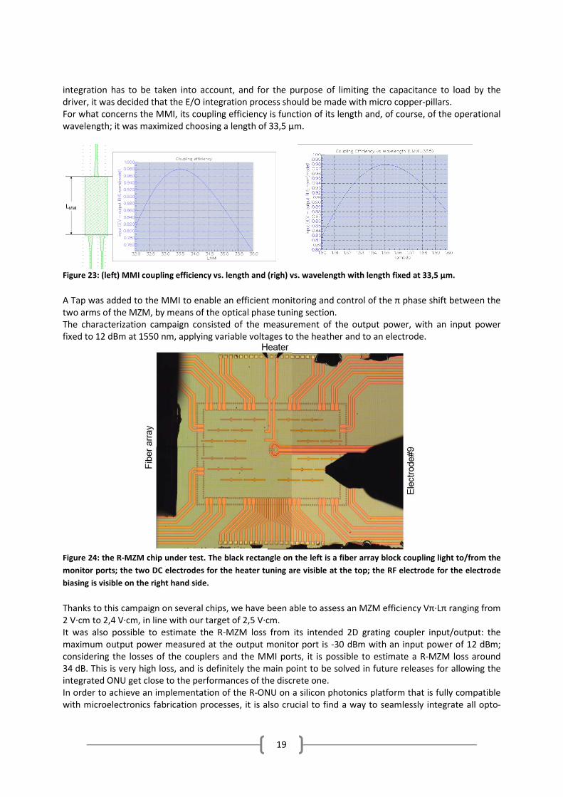
integration has to be taken into account, and for the purpose of limiting the capacitance to load by the driver, it was decided that the E/O integration process should be made with micro copper-pillars. For what concerns the MMI, its coupling efficiency is function of its length and, of course, of the operational wavelength; it was maximized choosing a length of 33,5 μm.
Figure 23: (left) MMI coupling efficiency vs. length and (righ) vs. wavelength with length fixed at 33,5 μm. A Tap was added to the MMI to enable an efficient monitoring and control of the π phase shift between the two arms of the MZM, by means of the optical phase tuning section. The characterization campaign consisted of the measurement of the output power, with an input power fixed to 12 dBm at 1550 nm, applying variable voltages to the heather and to an electrode.
Figure 24: the R-MZM chip under test. The black rectangle on the left is a fiber array block coupling light to/from the monitor ports; the two DC electrodes for the heater tuning are visible at the top; the RF electrode for the electrode biasing is visible on the right hand side. Thanks to this campaign on several chips, we have been able to assess an MZM efficiency Vπ·Lπ ranging from 2 V·cm to 2,4 V·cm, in line with our target of 2,5 V·cm. It was also possible to estimate the R-MZM loss from its intended 2D grating coupler input/output: the maximum output power measured at the output monitor port is -30 dBm with an input power of 12 dBm; considering the losses of the couplers and the MMI ports, it is possible to estimate a R-MZM loss around 34 dB. This is very high loss, and is definitely the main point to be solved in future releases for allowing the integrated ONU get close to the performances of the discrete one. In order to achieve an implementation of the R-ONU on a silicon photonics platform that is fully compatible with microelectronics fabrication processes, it is also crucial to find a way to seamlessly integrate all opto-

20
electronic building blocks. This is particularly challenging for the SOA, since it cannot be directly fabricated from the standard materials used in a silicon platform. An additional gain material has to be introduced without disturbing the process flow of other components and without impairing their performance. The route chosen within the FABULOUS project is the hybrid integration of InP-based material on SOI through wafer bonding. After the fabrication of all waveguides on SOI, the SOI wafer is planarized, and a III-V wafer is bonded on top of it. Then, the SOA material is processed such that it can amplify the optical mode present in the silicon photonics circuitry.
Figure 25: (top) Schematic view of the active region of a hybrid SOA, including taper structure; (bottom) cross-sections of the waveguides at different locations along the device, including field plots of the corresponding modes.
Figure 26: (a) Cross-sectional SEM picture of a hybrid waveguide with white lines added to make the silicon waveguide visible; (b) schematic cross-section.
The upper part of Fig. 25 shows the SOI and III-V waveguides in yellow and purple, respectively. The tapering in the waveguides causes the effective refractive indices to vary. The lower part of the figure shows the cross-sectional field distributions at three specific locations along the device. A mode that is dominantly confined to the SOI (left) can be transformed into a mode dominantly confined to the III-V material (right) when the effective refractive indices of the two modes match (center). The length of the taper structure in the current configuration is 150 μm. Computed coupling efficiencies are around 95% - 97% (using the commercial software FIMMWAVE of Photon Design). We believe that the majority of the residual energy goes into higher-order modes or is diffracted away from the waveguides, and very little will be reflected back into the fundamental mode of the waveguide. The fabrication of the SOI part is identical to the process flow of all other waveguide devices. The first step is the formation of passive rib waveguides by partially etching the guiding silicon layer. The remaining silicon layer in the etched areas has a thickness of 220 nm. To planarize the surface of the SOI wafer, a silica layer is deposited and then reduced by chemical-mechanical polishing. A uniform and smooth surface is crucial for the bonding of the active III-V wafer. The material used for bonding are 2’’ InP wafers that consist of a p-InGaAs contact layer, a p-InP cladding layer, 6 InGaAsP quantum wells surrounded by two InGaAsP separate confinement heterostructure layers, and an n-InP layer. After wafer bonding and InP substrate removal, dry etching is used to etch through the InGaAs layer and partly etch the InP p-doped waveguide cladding layer. The InP etching is completed by chemical selective etching. The MQW layer is etched by CH4:H2 RIE. Fig. 26 (a) shows a scanning electron microscope (SEM) picture of a III-V waveguide on top of a silicon waveguide, (b) shows the schematic cross-section. During the course of the project several version of the SOA were realized and packaged for testing; the following results refer to a unit having a gain section 1200 μm long and grating couplers for vertical (10° tilt) output coupling. Amplified stimulated emission (ASE) was measured with a drive current of 50 mA, at different temperature levels. Spectra are smooth and do not contain any parasitic lasing peaks, while ASE power level is still remarkable at 70°.

21
Figure 27: ASE spectrum at 50 mA drive current vs. temperature
Figure 28: Internal gain vs. drive current.
Internal gain was measured feeding the SOA with a 1560 nm wavelength using different bias currents and operational temperatures, with the setup causing a 7 dB grating coupler loss on both sided. A promising gain up to 23 dB was obtained at 40°C and 70 mA, with a saturation power between 3 dBm and 6 dBm. In Fig. 29 it is reported the output spectrum at 20°C with a bias current of 54 mA using three different input signals: 1540 nm, 1550 nm and 1560 nm, with input power levels of -35 dBm and -2 dBm. Is is possible to observe the saturation of the SOA at high input signal level with a decreased ASE power level.
Figure 29: output spectrum feeding the SOA with three different wavelengths. It is important to mention that all values seen in pictures suffer or the coupling losses for the stand-alone component measurement setup, that have been subtracted to evaluate the internal gain. Noise Figure (NF) was computed to range from 7 dB to 10 dB. The SOA has then proven to be a very interesting sub-product of the project, that can have interest for several other applications. The electronic driver (EIC) has been designed in a standard 65nm CMOS technology. It makes use of a multistage architecture, in order to provide the required voltage levels along the whole modulator structure without suffering from the unavoidable propagation attenuation featured by integrated transmission lines. Besides the straightforward technical challenges set by the required performances, the EIC had to be designed to consider the fact it had to be flip-chipped on top of the PIC, increasing the number of constraints. Each driver stage is designed to generate at the output a differential signal with 1.6V peak-to-peak amplitude, starting from a 340mV peak-to-peak differential signal at the input of the active delay chain. The output of each driver stage is AC coupled to the HSPM electrodes using an integrated MIM capacitor,

22
realizing a low frequency pole at ~3MHz. Each HSPM is differentially driven. The reverse bias voltage of each HSPM electrode is provided by two dedicated supply, one per electrode: reverse voltages in the range of 1.5V (e.g. V1=0.5V, V2=2V) can be safely used, without risks for the MIM capacitor. Two symmetric drivers have been realized for co-contra modulation, one per MZM arm. On each MZM arm, 12 differential driver stages (one every 500um) based on CML differential pairs with inductive peaking have been used. The delay matching between optical and electrical domains has been ensured at the center of each 500um-long section, making use of programmable active delay matching between 1mm-long adjacent MZM sections and of programmable passive delay matching within each 1mm-long MZM section. In order to verify the standalone electrical performance of the driver, a dedicated version for electrical testing has been integrated. This version includes a whole 6 delay elements chain (each element setting the delay between 1mm-long HSPM segments), the passive delay lines setting the delay between 500-um long segments, and the 4 the output driver stages receiving the signal from the first and last active delay elements (driver 1 and 2 from the first delay element, driver 11 and 12 from the last delay element). Since this version is supposed to be electrically probe tested, a lower gain is expected compared to the electro-optical version, due to the 100ohm differential load added at the output, in parallel to the integrated capacitance that mimics the load of each modulator stage.
Figure 30: EIC version for probe testing
Figure 31: transfer function of the drive in the probe-testing version.
The measured performances were as follows:
Parameter Measured value Note
Input matching < -12 dB up to over 30 GHz 100 Ὠ differential Driver DC gain (small signal) 10 dB On 100 Ὠ differential load
Driver -3dB bandwidth (small signal) 8 GHz to 10,3 GHz On 100 Ὠ differential load Driver DC gain (340 mVppd input) 4,5 dB to 8,2 dB
Output THD (340 mVppd input) < -17 dB
Active delay 20 ps to 28 ps @ 3 GHz 22 ps to 26 ps @ 8 GHz
Passive delay 8 ps Tunable in the E/O version At least in the version for probe-testing, the EIC has proven good match with the specifications. Realizing a partially integrated ONU with the R-MZM and the electrical driver flip-chipped on top required a few production lots of the SiP device and several steps to find the perfect flip-chipping process. The third lot of the R-MZM was the one providing the best optical performances, thanks a newly applied “optical access”

23
processing step with respect to the other lots, where an extra etching-step is applied, to remove the metallization processing-layers over the grating-couplers. To work with this lot offering improved optical performance, a new wire-bonding technique was required. A procedure with high contacting pressure, more aggressive ultra-sonic bonding, and hotter temperatures was used; somewhat surprisingly, no issues were encountered with the flip-chip and solder-reflow bonding of the driver to SiP chip. We speculate that the “no clean” flux used in the solder-reflow process is sufficient to displace or dissolve any contaminants on the copper-pillar-bump contact-pads.
Figure 32: Photograph of a photonic sub-assembly in the FABULOUS project, formed by the flip-chip integration of a PIC and driver Electronic-IC, with microscope image of the DC bond-pads
Figure 33: Fibre-to-Fibre transmission through the optical-shunt on a PIC from the third fabrication lot at CEA-Leti and detail on the grating couplers of different lots.
The test-setup for this partially integrated ONU was an exact transposition of the FDMA-PON transmission link, and the Error Vector Magnitude (EVM) was evaluated with off-line processing, being an important parameter for evaluating multilevel phase and quadrature modulation formats. In Fig. 34 such parameter is measured as a function of the frequency (which is allocated to the ONU) as the light polarization is randomly rotated over 100 states on the way to the ONU, in order to demonstrate the insensitivity to input polarizations. In Fig. 35, the same parameter is measured, given an operating frequency of 3 GHz, as a function of the input power.
Figure 34: Measured EVM (in dB) as a function of the user carrier frequency for both QPSK and 16-QAM signals over 100 states of polarization.
Figure 35: Median measured EVM against input power over 100 states of polarization.
1 2 3 4 5 6 7 8-18
-16
-14
-12
-10
-8
-6
fRF, GHz
EVM
, dB
Median Measured EVM over 100 states of polarization
Measured EVM (PIN= 7.5dBm, Lfiber= 0km)EVM for 2.e-3 BER with QPSK modulationEVM for 2.e-3 BER with 16-QAM modulation
2 3 4 5 6 7-18
-16
-14
-12
-10
-8
-6
PIN, dBm
EVM
, dB
Median Measured EVM over 100 states of polarizationfRF = 3GHz, PC=7.5dBm
Lfiber= 0kmLfiber= 10kmEVM for 2.e-3 BER with QPSK modEVM for 2.e-3 BER with 16-QAM mod

24
Based on these results, the partially integrated ONU relying on the third lot of R-MZM PIC was chosen to be inserted in the full system demonstrator. Attempts have been made to realize another version of the integrated ONU, using a Travelling Wave MZM instead of the segmented version, not needing the electrical driver and thus providing the space for bonding the SOAs: at the current state, no interesting result has been achieved, and some additional work needs to be carried out to improve the bonding and reworking process to avoid damaging the full PIC, as it has happened so far. The consortium is continuing this activity even after the end of the project as it is considered very promising and a fundamental step towards exploitation.
Inserting the PIC in the full system
The final FABULOUS experiment has been conducted realizing an ONU with one of the PIC previously described. In particular the device is composed by:
a silicon chip with a PBS and a segmented MZM, chosen to overcome the trade-offs of traditional travelling wave electrodes modulators. Each arm is segmented into 12 phase modulation sections with length of 500 μm each. Considering one single section, no propagation effects have to be taken into account and a simple lumped circuit model can be used. Besides, the required voltage levels along the whole modulator-arm-electrodes can be guaranteed without suffering from the propagation attenuation featured by integrated transmission lines. For the R-MZM reported here, only 6 out of 12 modulation sections were made active (i.e. L =3 mm). The reason for having limited the number of active doped sections is to limit the R-MZM losses. At the same time, this limits the signal strength. The R-MZM round trip losses are therefore estimated to be Loss ~17.5 dB.
an electrical driver EIC was fabricated on STMicroelectronics 65 nm CMOS technology. On each MZM arm, 12 differential driving stages are used, based on Current Mode Logic differential pairs with inductive peaking. The driving stages for each pair of adjacent 500 μm-phase-modulation-sections can be independently switched ON/OFF. The delay matching between the optical and electrical waves is ensured by making use of active delay matching between 1 mm-long MZM sections, and of passive delay matching within each pair of 500μm-modulation-sections. The active delay chain has been designed as a cascade of 6 active delay elements, each featuring a programmable delay (set to 24.5 ps). The nominal differential signal at the input of the active delay chain at f =3 GHz is 340 mVpp. Each driving stage is designed to generate at the output a 1.6 Vpp differential signal which is AC coupled to the phase-modulation-section-electrodes using an integrated MIM capacitor, and achieving a low frequency pole at 3 MHz. This EIC driver is flip-chip mounted on the Si-PIC using 20 μm diameter (40 μm pitch) copper pillars which were deposited on the EIC wafer. These copper pillars are capped with a SnAgCu eutectic solder layer. The corresponding bond pads on the Si-PIC consist of Al with a Ti/Ni/Au Under Bump Metallization (UBM).
test PCBs, consisting of three layers with a Rogers-4350B interposer for wire-bonding to the PIC, and containing MSMP-connectors for the RF signals, with surface-mounted electrical components to handle the DC signals. The EIC/PIC assembly is attached to the PCB using Au wire-bonding, together with an Al heat-spreader and a Thermo Electric Cooler (TEC). An 8-channel fibre-array is aligned and bonded to the grating-couplers on the Si-PIC. Fibre-to-PIC alignment is achieved using active optical feedback through 1D shunt GCs (Errore. L'origine riferimento non è stata trovata.). The fibre-to-fibre transmission is -11 dB, indicating a coupling insertion loss of -5.5 dB for each grating coupler.
In the following figure it is possible to see the PIC with the EIC flip-chipped on top, a detail of the fiber array coupled to the PIC and the test board used for system experiments.

25
Figure 36: Top left: silicon R-MZM with electrical driver flip-chipped on top, mounted on the test-board. Top right: fiber array coupled to the PIC. Bottom: the full test board.
A preliminary set of experiments on this board has been carried out with the post processing approach to characterize the PIC+EIC as stand-alone device, without any fiber but with VOA only. In the following figures some of the best constellations measured are reported: a QPSK and a 16-QAM with EVM=12%. Although these results are very promising, 16-QAM seems then not suitable for transmission with this prototype of the device.
Figure 37: QPSK constellation with EVM=12%
Figure 38: 16-QAM constellation with EVM=12%
As this device does not include the hybrid SOA, external optical amplification is needed for system test in the full network setup, and is provided by a discrete SOA. The setup for this test is shown in the following figure for the real-time experiments, however some results coming from full system off-line measurements are reported as well. In this case, the ODN is composed by 25 Km of optical fiber, to introduce dispersion, and a variable optical attenuator to span over a wider range of ODN-loss values. The required commercial SOA is inserted before the test-board and is then used bidirectionally: not the best working condition, thus adding

26
additional impairment. An IQ modulator is used to generate the modulating signals feeding the driver, starting from the baseband intensity-modulated sequences generated by the FPGA.
Figure 39: setup of the system experiment with the photonic circuit, with FPGAs for real-time transmission. Off-line characterization is made using a AWG at the ONU and a RTO at the OLT.
The full portable ONU for live demos is shown in the following picture:
Figure 40: the portable ONU using the integrated R-MZM in its test-board. It also includes FPGAs, clock distribution boards, voltage distribution boards, SOA diver, IQ modulator.
As previously mentioned, this R-MZM unit has proven not to be suitable yet for 16-QAM transmission, so we made the system campaign using QPSK modulation with a bandwidth of 330 MHz per user, yielding a net user bit-rate of 500 Mbps. With the 25 Km fiber and with the VOA set to 0, the EVM=12% obtained in back-

27
to-back condition is confirmed, granting no errors over more than 1 million symbols acquired. Acting on the VOA for spanning different attenuation values, an ODN loss of 24 dB is achieved considering the best FEC mentioned in the previous paragraphs; this value is far from the 31 dB target, but it was expected given the high insertion loss of the R-MZM, as previously mentioned in this section.
Figure 41: Top left: received constellation. Top right: constellation after equalization. Bottom left: constellation after equalization and carrier-phase estimation. Bottom right: normalized Power Spectral Density.
Figure 42: BER vs. ODN loss. Considering a FEC capable of correcting up to 10-2, the achievable loss is about 24 dB including 25 Km of optical fiber.
A long-term error count has been performed using a sub-optimal FEC, capable of correcting up to about 10-4, achieving uninterrupted transmission for 48 hours, demonstrating the good stability of the system. In conclusion, the insertion of the integrated ONU in the system has not brought new results with respect to what discussed in the previous sections, but has demonstrated that the FABULOUS PIC is feasible and functional, even if still far from the performances that discrete components available so far, and that the FABULOUS architecture is performing and stable, and the DSP as well is reasonably realizable on commercial FPGA platforms and ASICs. Given the higher than expected insertion loss of the integrated R-MZM, we are confident that newer versions will allow getting closer to the results achieved with discrete components.
1.1.4 Potential Impact, Main Dissemination Activities, Exploitation
Potential Impact
FABULOUS clearly targets broadband deployment in a Broadband-For-All policy, considering Fiber-to-the-Home (FTTH) or Fiber-to-the-Building (FTTB) + LAN services, as optical fiber the most future-proof transmission medium for avoiding new networks to become inadequate too soon. The advantages of a massive broadband deployment are now universally accepted, and being optical fibers capabilities virtually unlimited, they are able to easily overcome copper, that has already come up to its fundamental physical limits, and mobile networks, that start experiencing scarcity of available spectrum. Do we really need the huge bandwidth fibers can provide? Maybe not today, but historically, as internet connection speeds have increased, new technologies and services have emerged: let’s think about what has happened, for example, to the quality of video-streaming services for residential customers in the recent years, being TV or vide-surveillance or conferencing services; in the end history teaches that if we have bandwidth, we will find the way to fill it, and operators as well have found that when their customers get access to more bandwidth, they use it! A virtuous circle can be created, as availability of broadband will
0 0.1 0.2 0.3-30
-20
-10
0
Frequency [GHz]
Normalized PSD [dB/Hz]
Sampled Demod Output (2 SpS)
-2 0 2-2
-1
0
1
2Equalized Signal (Blind Equalizer)
-2 0 2-2
-1
0
1
2
Signal after CPE
-2 0 2-2
-1
0
1
2
20 21 22 23 24 2510-5
10-4
10-3
10-2
10-1
100
ODNLOSS [dB]BE
R
FEC threshold

28
enable new services, and the presence of new services will increase broadband demand. The empirical “Nielsen’s Law of Internet Bandwidth” states that a high-end user’s connection speed grows by 50% every years, doubling every 21 months, and as bit-rate requirements increase, technology needs to remain one step ahead. The first straightforward comment that can be made, is that FTTH/B creates direct job opportunities in the installation phase: this would seem trivial, but is not of secondary importance if we consider the household penetration of FTTH/B services in Europe at end of Sept. 2015: excluding Russia, all European bigger countries have a penetration lower that 12%, with Germany just above 1%; this means that there still is an incredible amount of work to be done, with a large employment potential, to which has to be added the potential creation of new ICT-related jobs. Isn’t this an opportunity, in a continent that still has troubles exiting the recession?
Figure 43: rankings of household penetration of fiber (FTTH and FTTB+LAN) services in Europe at sept. 2015, considering economies with at least 200000 households. Source: FTTH Council Europe, February 2016. The development of a fast network has also many sustainability implications, enabling teleworking, e-health, remote medical assistance, e-government, reducing for example traffic and pollution. Moreover, the excess bandwidth provided by fiber networks could easily host smart meters data, without needing dedicated networks for the smart grids. To wrap up, it is interesting to mention that the Organisation for Economic Cooperation and Development (OECD) states that the cost of national FTTH networks would be justified by 10 years of cost savings of between 0.5% and 1.5% over 10 years in each of the electricity, transport, energy, and health-care sectors resulting directly from broadband deployment. The impact of FTTH/B deployment is then obvious and very meaningful, very deeply analyzed by consultants, policy makers, the EU commission, etc. But where does FABULOUS stand in all this? Of course FABULOUS is not enabling this process, but together with other projects and activities can definitely contributing in speeding it up, as it has demonstrated that:
Splitter based PON, provided that the correct technology is chosen, can already today grant high capacities for the access network, to the private homes as well, and are scalable without the need to impact on the existing infrastructure;

29
Silicon photonics is not far from being a mature technology for allowing performing optical devices with target prices for broadband optical cards typical of the consumer electronic market. It could be argued that most of the cost of PON deployment is in the infrastructure, and that is definitely true, but as backwards compatibility with existing PON is granted, lowering the cost of the equipment is meaningful as well.
The role of standards in telecommunications equipment is of primary importance, and FABULOUS as a potential impact on standardization actions as well. As mentioned in the “Project context and objectives” section, there still are some open technological issues for mass production of G.989 equipment, in particular related to the unavailability of low cost tunable lasers for the ONU, could slow-down G.989 deployment, to the point that some alternatives are currently being sought, in particular for increasing the aggregate capacity on a single wavelength rather than increasing the number of wavelengths. The main challenges of increasing the serial bitrate beyond 10 Gbps are decreased chromatic dispersion tolerance, increased bandwidth requirements of the optical and electrical components and the resulting reduced power budget and fiber reach, together with an higher overall system cost. To address these challenges, the FSAN is now investigating alternative low complexity modulation formats that require less bandwidth and/or are more tolerant to chromatic dispersion, targeting inline bitrates of 25 Gbps and 40 Gbps. Considering Intensity Modulated Direct Detection (IM-DD) modulation schemes for upgrading the serial bitrate at the lowest cost, NRZ, Quaternary Pulse Amplitude Modulation (PAM-4), Electrical DuoBinary (EDB) and Optical DuoBinary (ODB) are the direct detection candidates that have been lately studied for achieving serial bitrates beyond 10 Gbps for use in high rate PON. Following the current path of the standardization bodies, and in order to reuse components, technologies and knowledge from legacy PONs, the future of optical networks will most probably continue to rely on TDM and WDM technologies, but the OFDM (Orthogonal Frequency Division Multiplexing) and FDM (Frequency Division Multiplexing) PONs could also bring solutions to provide higher bit rates. There will be required colorless technologies providing very high bit rates (100G). Potential technological candidates already exist, resulting of intensive research studies and the proposal and results about FDM PONs brought by FABULOUS is definitely one of them. Results coming from FABULOUS could actually have an impact of more general nature for the silicon photonics community and related devices manufacturers as well. It is in general perceived that the next few years will be of paramount importance for coming to a “go/no go” answer on the debate on the adoption of silicon devices in optics; let’s consider the market of data-centers, the so called optical interconnect. There currently are about 500.000 data-centers in the world, each of them having thousands of optical interfaces; the number of interfaces unceasingly continues to grow, as all internet traffic passes through these data-centers, and most of the traffic is anyway within the data-center! If we again consider the Nielsen’s law about internet traffic growth, we can have an idea of the demand of components for optical interconnect: the potential market for silicon here is huge and cannot be missed; however, the technology is not yet fully mature. The SOA demonstrated by III-VLab is a fundamental building block for allowing silicon become dominant in this market, in order to counteract to silicon devices insertion loss and to enable photonic integrated circuits performing more complex functions. To this end, the wire-bonding of the SOA on the silicon modulator in FABULOUS has not been fully successful, but encouraging results have been achieved showing the path towards an efficient integration process, to the point that III-VLab, as explained later, foresees commercialization starting from 2020. The impact on European industries as components and equipment suppliers to data-centers, hard to be estimated in numbers, would for sure be huge.
Dissemination Activities
As the scientific objectives of FABULOUS were well beyond the state-of-the-art at the time of the project start, an obvious focus on pure scientific dissemination has heavily been put, also thanks to the presence of universities and research centers; results have been outstanding, as more than 10 journals with peer-review process and impact factor have been published within this 45-months period, and tens of talks at scientific conferences were given. It is worth nothing that the results relevance was so widely accepted by the scientific community, that about half of the journal papers were of invited nature. In some cases, the

30
participation at scientific conferences was not only limited to paper presentations, but coupled to the presence at the associated exhibitions and with live demos: this happened OFC/NFOEC 2013, ECOC 2014, EUCNC 2014 and FOTONICA 2015. As silicon photonics is a very hot topic in this recent years from the industrial point of view as well, the FABULOUS coordinator has been invited to give invited talks a couple events in which renowned scientists from all over the world are invited to give keynote speeches on the state-of-the-art and on vision on technology for the purpose of industries and operators: in particular he has been invited at the first edition the PIC International and at the 18th edition of the Next-Generation Optical Networks, the first one being oriented to industries in general and the second one being oriented to telecom operators in particular. However, to the ends of FABULOUS, the most important industry-oriented event of showcase has been the presentation given at an FSAN meeting in October 2015, being FSAN the initiative that suggested G.989 to ITU-T: this can be considered at the same time a dissemination and an exploitation action, as hopefully will bring opportunities for FABULOUS in new releases of PON standards.
Figure 44: presenting the FABULOUS approach to photonic integration at PIC 2016.
Figure 45: FABULOUS roll-up at the III-VLAB booth at OFC/NFOEC 2013.
The presence of universities in the consortium gave FABULOUS the possibility to be presented at students as well, with presentations from the coordinator to the students of the University of Pavia in two editions of PhD seminars and at the students of Politecnico di Torino at the launching day of the Turin Students OSA Chapter. FABULOUS also tried to address the wider general public, so that the FABULOUS coordinators managed to be interviewed by important Italian newspapers, such as La Repubblica and Il Sole 24 Ore, and a feature appeared on The Parliament Magazine. Last but not least, besides the project website, a periodic newsletter was realized in 4 issues and electronically sent to a recipient of about 700 stakeholders.
Exploitation
Both the architectural concept and the technological results of FABULOUS are expected to have importance for the medium term and not only immediately after the end of the project, for a few main reasons. First of all, EU has set the following broadband deployment targets for EU citizens:
ensuring access to all Europeans to internet speeds of above 30 Mbps by 2020;
31
ensuring that at least 50% of European households subscribe to internet connections of above 100 Mbps.
These targets are still very far to come and, very differently from Japan and South Corea, but for sure massive PON deployment is a key for reaching them. In addition, Silicon Photonics is still a relatively young technology with respect to semiconductor, but some form of optical integration seems mandatory for reaching at least 50% of households; as a consequence, exploitation of our results will need to be pursued for many years to come, and the consortium is accordingly committed. The main exploitation action foreseen by the FABULOUS consortium is related to the full architecture and its original purposes of a PON capable of tens of Gbps over X-GPON ODN: even if G.989 has been standardized during the course of the project, its performances are still lower than the FABULOUS ones and thus the original purpose still makes sense for future PON generations. This action is being carried out, mostly thanks partner ORANGE, through the FSAN initiative and, as previously mentioned, has already started presenting FABULOUS at an FSAN meeting in Atlanta in October 2015. It is worth mentioning that one of the main problems that drove the project concept, in particular the difficulty of realizing low cost tunable lasers on a 50 GHz or 100 GHz, is still very actual and apparently some rethinking about G.989 is going-on, as increasing the bit-rate per wavelength appears more feasible than increasing the number of wavelengths: definitely an opportunity, if not for the FABULOUS PIC, at least for the FABULOUS architecture, that will be pursued by ORANGE still after the end of the project, as standardization is a long process. This definitely improves the preliminary sensation about standardization that was reported in the Intermediate plan for use and dissemination released in April 2014. Besides the PON application, the effectiveness of the architecture could also be of interest for the field of Passive Optical LAN (POL), that is the use of optical technologies for local area networking, and as testified by NOKIA on Lightwave Magazine6, it is going to be the next frontier for business buildings cabling for reducing installation and maintenance cost, as well as energetic impact, while providing a performance increase that copper cannot grant; the FABULOUS partners are already working to liaise with industrial actors in this field. STMicroelectronics has confirmed its intention to make business on their silicon photonics fab, targeting applications requiring millions pieces per year; for the short term, PON doesn’t seem an application field capable of granting such numbers, but it will when further investments on fiber infrastructures will be made, such as the one that has recently been launched in Italy by Enel Open Fiber. For the short term, the most promising communications scenario for silicon appears to be Optical Interconnect, that has the advantage not to be subject to massive standardization. Also sub-products of FABULOUS have an exploitation potential. For example, III-V Lab developed hybrid III-V semiconductor optical amplifiers (SOAs) on silicon, and also the integration of the SOAs with silicon modulators. The standalone SOAs, as well as the SOAs integrated in the final demonstrators, exhibit the state of art performance (internal gain > 15 dB, and output power level > 10 dBm). It is the intention of III-V Lab to make industrial exploitation of the photonic integrated circuits on silicon incorporating the SOAs for optical communication applications. The achievements of Fabulous project on SOAs constitute a new milestone towards such a purpose. However, further research is still necessary in order to push the SOA performance, in particular, the output power level. Industrial exploitation of the hybrid III-V/Si technology is expected to begin around 2020, targeting in particular application for short reach (< 2 km) and medium reach (< 40 km) communication applications. Similar directions could be pursued for the R-MZM designed by CEA-Leti, that is does not necessarily needs FDMA to be employed, or in a version without reflectivity feature for application in very short reach environment such as the Optical Interconnect, and the same applies, for example, to the design of optical filters, that could be also widely reused in other fields such as sensing.
6 “Why now may be the time to rethink your LAN strategy”, Lightwave Magazine online, 1st July 2016, http://www.lightwaveonline.com/articles/2016/07/why-now-may-be-the-time-to-rethink-your-lan-strategy.html

32
Much knowledge has been generated in terms of algorithms as well, to the point of real-time implementation on FPGA platforms, and for example the algorithms for self-coherent receivers in the FDMA environment have potential application for future front-hauling applications, and can definitely become useful background for generating projects in the next EU calls about 5G. Exploitable foreground of different nature is related to processes that could be offered as services; for example, the "no clean" flux solder re-flow process for flip-chip integration, developed for FABULOUS by Tyndall, will be offered to the wider European Photonics community through the EuroPractice / ePIXfab access programmes: http://www.europractice-ic.com/SiPhotonics_technology_description.php The Photonics Packaging Group at Tyndall supports academic and spin-out users of the Si-Photonics multi-project wafer (MPW) runs of EuroPractice by developing packaging design rules (PDRs) and offering low-cost generic packages that provide electrical, optical, and thermal access to the MPW fabricated Si-PICs. These PDRs have been developed into software templates allowing users to more easily design SI-PICs that conform to packaging standards and best-practices. The Photonics Packaging Group is continuously working to expand the catalogue of generic packaging techniques it can offer to EuroPractice. Tyndall is working to add a flip-chip integration process to users, based on the "no clean" flux solder re-flow process developed and implemented for the FABULOUS project, and expect it to be ready by the end of 2016. Adding this technique to EuroPractice will remove the existing high-cost barrier of developing and testing high-speed Si-PICs with integrated drivers, helping to promote innovation and invention in European researchers and SMEs.
1.1.5 Project website and logo
Project contact
Silvio Abrate – Project Coordinator Head of Applied Photonics Istituto Superiore Mario Boella (ISMB) via P.C. Boggio 61, 10138 Torino (Italy) e-mail: [email protected] office: +39 011 2276302
Fabulous logo and website
The FABULOUS website, www.fabulous-project.eu, has been used as a key channel to disseminate the overall project and all relevant results achieved. It has been regularly updated during the whole project duration. The FABULOUS logo is used in all materials produced within the project:

33
Figure 46: the FABULOUS logo.
Other consortium contacts
Roberto Gaudino Politecnico di Torino – Dipartimento di Elettronica e Telecomunicazioni [email protected] Benoit Charbonnier CEA-Leti [email protected] Enrico Temporiti STMicroelectronics [email protected] Guido Giuliani University of Pavia [email protected] Peter O’Brien Tyndall National Institute [email protected] Guang-Hua Duan III-V Lab [email protected] Fabienne Saliou
