fabrication of nitrogen-containing coatings in reed ... · journal of surface investigation: x-ray,...
TRANSCRIPT
1106
ISSN 1027-4510, Journal of Surface Investigation: X-ray, Synchrotron and Neutron Techniques, 2016, Vol. 10, No. 5, pp. 1106–1118. © Pleiades Publishing, Ltd., 2016.
Fabrication of Nitrogen-Containing Coatings in Reed Switchesby Pulsed Ion-Plasma Treatment1
I. A. Zeltsera, V. S. Gurovb, N. B. Rybinb, A. Tolstogouzovb, c, *, D. J. Fud, and Pravin Kumare
aRyazan Metal Ceramics Instrumentation Plant Joint Stock Company (RMCIP JSC),Novaya Str. 51 V, 390027 Ryazan, Russian Federation
bRyazan State Radio Engineering University (RSREU), Gagarin Str. 59/1, 390005 Ryazan, Russian FederationcCentre for Physics and Technological Research (CeFITec), Dept. de Física da Faculdade de Ciências e Tecnologia (FCT),
Universidade Nova de Lisboa, 2829-516 Caparica, PortugaldSchool of Physics & Technology, Wuhan University, 430072 Wuhan, China
eInter University Accelerator Centre (IUAC), Aruna Asaf Ali Marg, 110067 New Delhi, India*e-mail: [email protected]
Received March 14, 2016
Abstract—We focus on the detailed characterization of the coatings produced by pulsed ion-plasma treatmenton contact surfaces of permalloy (iron-nickel) blades directly in nitrogen-filled reed switches. The measure-ments of electrical resistance, breakdown voltage and return factor of reed switches were carried out in situprior to and after ion-plasma treatment, and the morphology and elemental (chemical) composition of thecoatings were monitored ex situ by means of scanning electron microscopy and energy dispersive X-raymicroanalysis. The main processes occurring on the contact surfaces in the course of ion-plasma treatmentwere discussed in the frame of anomalous glow and arc discharges theories by Mesyats. It was shown that ion-plasma treatment allows fabrication of erosion- and corrosion-resistant nitrogenated iron-nickel coatingswith the electrical resistance of 0.1 Ohm. In the optimal symmetrical mode with the processing time of ca. 7min the nitrogen concentration in the coatings was estimated of 20 at %. Higher and lower nitrogen contentand the presence of oxygen in the coatings showed negative influence on the electrical resistance, whichdetermines the quality of reed switches. Prototype models of the reed switches with nitrogenated coatings suc-cessfully passed switchgear reliability tests and demonstrated the competitive capacity as regards the standardreed switches with electroplating coatings based on the noble metals.
Keywords: arc discharge, energy dispersive X-ray microanalysis, ion-plasma treatment, nitrogenated coat-ings, reed switch, scanning electron microscopyDOI: 10.1134/S1027451016050190
1. INTRODUCTION
Reed switch (RS) is a compact electromechanicalcommutator of millimeter dimension composed oftwo ferromagnetic electrodes (blades or contacts)placed in nitrogen-filled or evacuated glass bulb.Under an influence of the external magnetic field, theblades pull together, and the switch closes. From thelate thirties, reed switches are widely used in differentswitchgear including military equipment, home elec-tronics, etc. At present time, the annual RS globalmarket exceeds billion items.
A high-quality reed switch is able performing 107–108 switchgear cycles, and during this its electricalresistance should be within the limit of 0.1 Ohm.However, electric discharges occurring in the courseof switching increase the resistance and decrease the
running time. To prevent such degradation, nonmag-netic protective coatings are deposited on the contactsurface of blades. For that, electroplating of noblemetals (gold, palladium, ruthenium, rhodium, etc.) iscommonly applicable. However, this widespread tech-nique has several disadvantages negatively affectingthe RS quality, surrounding environment and healthof the service personnel [1]. Besides, it is not cost-effective since the production of every thousand reedswitches requires ca. 0.15 grams of expensive noblemetals.
As an alternative approach, we proposed to usepulsed ion-plasma treatment (PIPT), both ion-plasma nitriding [1–3] and ion-plasma deposition [4–6], for fabrication of the protective nitrogen-contain-ing coatings on the contact surface of permalloy (iron-nickel) blades directly in the sealed reed switches. Inthat case, a reed switch is considered as a simple diodesystem, where the blades act as electrodes (cathode1 The article is published in the original.
JOURNAL OF SURFACE INVESTIGATION: X-RAY, SYNCHROTRON AND NEUTRON TECHNIQUES Vol. 10 No. 5 2016
FABRICATION OF NITROGEN-CONTAINING COATINGS 1107
and anode, target and substrate), and the glass bulbfilled by nitrogen serves as a working chamber.Depending on PIPT regime, mainly on the duration τof voltage pulses applied to the open contacts, nitrideand oxy-nitride iron and nickel coatings of differentstructure and composition were produced. Usingsputter depth profiling by a time-of-flight secondaryion mass spectrometer TOF. SIMS-5, the thickness ofthese coatings was estimated in the range of 20–25 nmfor ion-plasma nitriding (τ = 2 µs) [3] and within 320–380 nm for ion-plasma deposition (τ = 20 µs) [5].
It was shown [1–6] that the developed technique isenvironment-friendly, more resource saving and cost-effective as compared with electroplating. PIPTensures required corrosion and erosion resistance ofblades and decreases the number of foreign particleson their surfaces, which are typical contaminants forelectroplating. However, the relatively high nitrogenpressure in a bulb (ca. 40 kPa) and the short distancebetween contacts (ca. 30 µm) promote the initiation ofarc discharges into the inter-electrode gap that, inturn, can have significant and unpredictable impacton the quality of reed switches. For example, the pres-ence of superposed craters of 1 µm in diameter withfritted breastworks of ca. 100 nm in height was revealedon the surface of contacts by scanning electronmicroscopy (SEM) [6]. Moreover, PIPT regime testedin [6] has demonstrated rather low efficiency since theprocessing time was ca. 30 min.
In this work, we provide a detailed morphologicaland elemental (chemical) description of the coatingsPIPT-produced on the contact surface of reedswitches. These measurements were coupled with thetesting of the electrical resistance, breakdown voltageand other electrophysical characteristics of reedswitches. Our ultimate purpose is an advanced study ofphysical processes occurring during pulsed ion-plasma treatment of reed switches and based on thefindings, the improving the efficiency of the coatingsfabrication.
2. MATERIALS AND METHODS
We studied the prototype models MKA-14701(Fig. 1) manufactured at RMCIP JSC (Ryazan, Rus-sian Federation) on the basis of commercially pro-duced reed switches MKA-14103 [4]. The main differ-ence of the prototype model as against standard RS isan absence of the gold-ruthenium electrodepositedcoatings on the contact surface of blades. Instead ofthose, nitrogen-containing iron and nickel coatingswere fabricated directly in reed switches using PIPTtechnique.
The blades were pressed of vacuum-melt permalloy(Ni 52 wt %, Fe 48 wt %) wires by Dilaton™,degreased and annealed in hydrogen atmosphere.When sealing the reed switch, the bulb was filled withdry pure (99.99%) nitrogen under the pressure withinthe range of (33–40) kPa.
The gap between parallel blades was 30 µm and theoverlapping (contact or working) region was of 400 µmin length and 680 µm in width. Ion-plasma treatmentwas carried out by means of high voltage pulses withthe duration of 20 µs and frequency of 1 kHz. Theform of the pulses was nearly rectangular, and they fol-lowed in groups (packets). Each individual group con-sisted of 5 single-polarity pulses.
Two ion-plasma treatment regimes, called PIPT-1and PIPT-2, with the different pulse amplitude A, theduration of the single treatment Tt and the pausebetween this treatment Tp were tested (Table 1). Sincereed switch production is a large-scale manufacturing,PIPT-2 regime looks preferable than PIPT-1 due tolower pulse amplitude and duration of the operatingcycle (treatment plus pause), which results in energyconservation and higher productivity.
The number of the operating cycles N reached 30and 40 for PIPT-1 and PIPT-2, respectively. In all, westudied 15 reed switches (S1-S15 samples) produced insymmetric and asymmetric modes. In both modes,one of the blades was always grounded. In symmetricmode (S1–S9 samples), the polarity of pulses, appliedto the other blade, was changed with the frequency of50 Hz, and in asymmetric mode (S10–S15 samples)the pulses polarity stayed invariable. It means that insymmetric mode each blade served by turns as cathodeand as anode, and in asymmetric mode the role ofblades became invariable.
The switchgear reliability tests and the measure-ments of electrophysical characteristics – electricalresistance R, breakdown voltage U, and the return fac-tor2 K, were carried out using special-purpose equip-ment and methods described elsewhere [1, 2, 4, 6].The reliability tests and electrophysical measurementswere made in situ, i.e. without mechanical destroyingof reed switches.
2 The return factor is estimated as a ratio of the release and oper-ating ampere-turns.
Fig. 1. External view of a reed switch MKA-1407.
Table 1. Characteristics of the pulsed ion-plasma treatmentregimes
PIPT regime A, kV Tt, s Tp, s Sample
IPT-1 2 30 30 S14, S15IPT-2 1.65 10 10 S1–S13
1108
JOURNAL OF SURFACE INVESTIGATION: X-RAY, SYNCHROTRON AND NEUTRON TECHNIQUES Vol. 10 No. 5 2016
ZELTSER et al.
The morphology and uniformity of the coatingsproduced were determined ex situ by a JEOL JSM-6610LV equipped with an energy dispersive X-raymicroanalyzer INCA X-MAX by Oxford Instrumentfor quantification of elemental (chemical) composi-tion of the samples. Prior to these measurements, glassbulbs were mechanically destroyed, and RS bladeswere extracted outside. No special cleaning or treat-ments of the blades were performed, except theremoving of residual small glass pieces from the con-tact surfaces by jet of pure nitrogen.
3. RESULTS3.1. Electrophysical Measurements
Ion-plasma treatment of the contact surfaces ofblades, both in symmetric and asymmetric modes, isinitiated by means of anomalous glow discharge(AGD). However, after a few operating cycles, arc dis-charge comes up to take the AGD’s place [1, 2].
In PIPT-1 regime, the AGD voltage and currentwere 280 V and 250 mA, respectively. Then, after theinitiation of arc discharge, the discharge voltage wasdramatically decreased to 12–20 V, and, on the con-trary, the discharge current increased and reached to280 mA. In PIPT-2 regime, the discharge current washigher—460 and 530 mA for anomalous glow and arcdischarges, respectively.
The electrophysical characteristics of reed switchesprior to and after ion-plasma treatment are presentedin Table 2. Mainly, we studied the samples after PIPT-2
since this regime is more efficient than PIPT-1 fromthe industrial point of view.
Initially, the breakdown voltage U0 of all sampleswas in the range of 280–290 V, and after PIPT its valuecalled Ut decreased to 200 V. Figure 2 shows thedependence of the normalized drop of breakdownvoltage ∆U = (U0 – Ut)/U0 versus the number of oper-ating cycles. For all regimes, ∆U exhibits an evidentincrease, and its final value reaches to 25–30% higherthan that of the initial value. During PIPT, the partialpressure of nitrogen in a RS bulb decreases sincenitrogen molecules and atoms participate in the for-mation of nitrogenated coatings on the contact sur-faces. The decrease of N2 pressure, occurring in theright part of the Paschen curve, causes decreasing ofthe breakdown voltage, and this drop becomes greaterwith an increase of the processing time. At the sametime, the nitrogen concentration in the coating and itsthickness increases. The return factor also increases. Itwas known [1, 4] that the K-value tends to increasewith an increasing of the concentration of paramag-netic compounds in the coatings as well as with anincreasing of the coating’s thickness. It is very likelythat the rise of the return factor could be caused by theformation of NinN compounds (n = 2, 3), which possessparamagnetic properties [7].
As regards the electrical resistance of reed switches,the best value was found to be 0.095 Ohm after 20operating cycles (sample S7, PITP-2, symmetricmode). However, for the other samples (see Table 2)
Table 2. Electrophysical characteristics of the reed switches before and after ion-plasma treatment
Sample Regime Mode NBefore/after ion-plasma treatment
U, V R, Ohm K
S1
PIPT-2
Symmetric
2 280/280 0.16/0.11 0.34/0.37
S2 4 290/270 0.17/0.10 0.34/0.37
S3 8 280/270 0.14/0.14 0.37/0.53
S4 10 290/260 0.14/0.10 0.35/0.45
S5 14 270/240 0.16/0.105 0.36/0.51
S6 18 280/230 0.15/0.11 0.37/0.53
S7 20 280/210 0.18/0.095 0.34/0.48
S8 30 290/210 0.16/0.11 0.34/0.58
S9 40 280/210 0.17/0.14 0.37/0.51
S10
Asymmetric
10 275/245 0.19/0.25 0.36/0.47
S11 20 290/220 0.16/0.21 0.34/0.57
S12 30 280/210 0.23/0.20 0.34/0.53
S13 40 290/200 0.16/0.32 0.37/0.60
S14PIPT-1
30 300/220 0.21/0.24 0.37/0.58
S15 30 295/200 0.22/0.25 0.36/0.54

JOURNAL OF SURFACE INVESTIGATION: X-RAY, SYNCHROTRON AND NEUTRON TECHNIQUES Vol. 10 No. 5 2016
FABRICATION OF NITROGEN-CONTAINING COATINGS 1109
the R-value remained practically invariable afterPIPT, within the range of 0.14–0.23 Ohm. It shouldbe noted that the processing time of ion-plasma treat-ment of the S7 sample was only 6.7 min, in 4.5 timeslower than in [6] by PITP-1 in symmetric mode.
The switchgear reliability tests showed that the pro-totype reed switches MKA-14701 produced in PITP-1and PIPT-2 regimes with the number of operatingcycles 30 and 20, respectively, are not inferior to thestandard devices in the respect of the running time andswitching power.
3.2. Scanning Electron Microscopy and Energy Dispersive X-ray Microanalysis
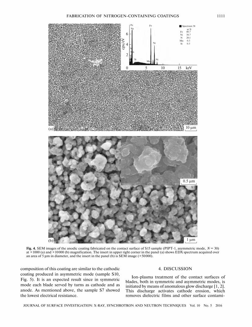
SEM images and energy dispersive X-ray (EDX)spectra measured for anodic and cathodic coatings onthe working surface of S15 sample are presented inFigs. 3 and 4. These coatings were fabricated in PIPT-1regime (N = 30) using asymmetric mode, i.e. thefunctions of blades during ion-plasma treatment werefixed.
The morphology of the cathodic coating is shownin Fig. 3. The superposed craters of 1–4 µm in diam-eter with fritted breastworks of ca. 100 nm in heightand 1 µm in width are seen on the surface. These cra-ters were caused by the action of mobile cathode spotsof 2d type arc discharge [8–10]. Since each cathode spotconsists of several cells one can see small craters of ca.70–100 nm in diameter on the walls of large craters andbreastwork’s surfaces. Similar large and small craterswere observed in [6] after PIPT-1 in symmetric mode.
The anodic coating (Fig. 4) radically differs fromthe cathodic one. It exhibits columnar structure com-
posed of the single columns (pillars) growing perpen-dicularly to the surface and contacting each other. Themost part of the columns are 300–500 nm in diameter.Each column consists of globules, of ca. 70 nm indiameter. Its external form resembles a bunch ofgrapes (insert in Fig. 4b). The globules of similar sizesand shapes are seen on the surface of cathodic coatings(insert in Fig. 3b). Such globules are called the dripcathodic spots [11, 12]. It is very likely that they repre-sent the solid drops of metals, which were molten byarc discharges and were not reached to the anode sur-face.
The nitrogen concentration in the cathodic (EDXspectrum in Fig. 3a) and anodic (EDX spectrum inFig. 4a) coatings was approximately the same, withinthe range of 20–23 at %. The presence of oxygen wasrevealed in anodic coatings. These data are compara-ble with those obtained in [6] after PIPT-1 in symmet-ric mode. It confirms the formation of nitrogenatedcoatings of the contact surfaces of blades.
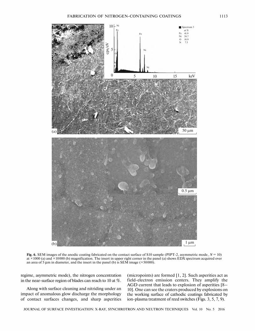
SEM images and EDX spectra measured foranodic and cathodic coatings fabricated in PIPT-2regime using asymmetric mode are shown in Figs. 5and 6 for S10 sample (N = 10) and in Figs. 7 and 8 forS13 sample (N = 40). The morphological features ofthe cathodic and anodic coatings are similar for bothsamples, and in general are similar to those shown inFigs. 3 and 4 for S15 sample discussed above. Anincrease of the processing time resulted in the rise ofthe nitrogen concentration, from 10 to 30–35 at % forthe number of operating cycles ranged from 2 to 40. Atthat, the nitrogen content at the bottom of craters wasfound to be half as much as compared with its value onthe breastwork’s surfaces. The oxygen concentrationwas ca. 5–10 at %, wjich did not change with the pro-cessing time.
For the cathodic coatings, the total quantity of cra-ters, as well as the number of craters with relativelylarge diameters, increased with an increase of N(Figs. 5 and 7). After 10 operating cycles, the surface ofthe sample S10 has become inhomogeneous (Fig. 5),with many small craters, having their diameters lessthan 1 µm. The larger craters, of 5 µm in diameter, arelocalized to the separate groups (Fig. 5a). It is verylikely that the small craters represent the traces ofcathode spots of 1st type arc discharge, and the largerones are caused by arc discharge of 2d type [10]. Pro-longed treatment stimulates the formation of the cra-ters by 2d type arc discharge (sample S13, Fig. 7). Thestructure of these craters is complex – small craters of0.5–1 µm in diameter located at the bottoms and onthe breastwork’s surfaces. Besides, tiny craters (70–100 nm in diameter) created by the cells of cathodespots are observed inside the small craters (Fig. 7b).
For anodic coatings, the concentration of globulesincreased with an increase of N (Figs. 6 and 8). Themorphology of anodic coatings has become similar to
Fig. 2. The normalized drop of breakdown voltage ∆U =(U0 – Ut)/U0, where U0 and Ut are the breakdown voltageprior to and after ion-plasma treatment, respectively, ver-sus the number of operating cycles for different PIPTregimes.
30 35 4025N20151050
5
10
15
20
25
30
35ΔU
/U0,
%
PIPT-2/Sym/S1−S9PIPT-2/ASym/S10−S13PIPT-1/ASym/S14PIPT-1/ASym/S15

1110
JOURNAL OF SURFACE INVESTIGATION: X-RAY, SYNCHROTRON AND NEUTRON TECHNIQUES Vol. 10 No. 5 2016
ZELTSER et al.
that observed for the sample S10 (Fig. 4), but onlyafter N = 40 (Fig. 8). The estimated minimal globule’sdiameter was 70 nm (insert in Fig. 8b) that is the sameas in case of the sample S10 (insert in Fig. 4b).
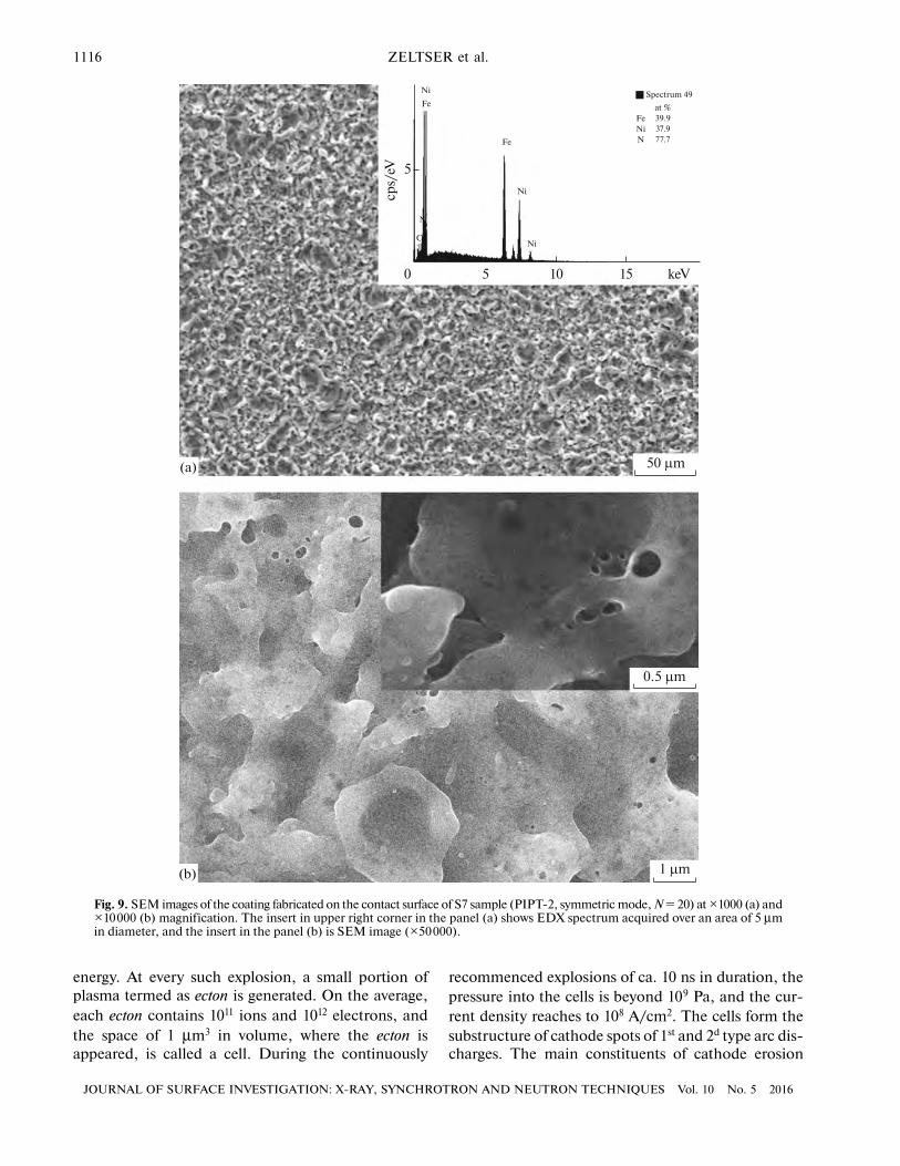
Figure 9 shows SEM images and EDX spectrummeasured for the coating fabricated on the contactsurface of the sample S7 (N = 20) in symmetric modeof PIPT-2 regime. The morphology and elemental
Fig. 3. SEM images of the cathodic coating fabricated on the contact surface of S15 sample (PIPT-1, asymmetric mode, N = 30)at ×1000 (a) and ×10000 (b) magnification. The insert in upper right corner in the panel (a) shows EDX spectrum acquired overan area of 5 µm in diameter, and the insert in the panel (b) is SEM image (×50000).
keV
cps/
eV
151050
Fe
15
(b)
10 μm
0.5 μm
1 μm
(a)
Ni
N
Mn
C
Fe
Mn Ni
Ni
FeNiN
Mn
Spectrum 43at %
38.538.322.70.5
JOURNAL OF SURFACE INVESTIGATION: X-RAY, SYNCHROTRON AND NEUTRON TECHNIQUES Vol. 10 No. 5 2016
FABRICATION OF NITROGEN-CONTAINING COATINGS 1111
composition of this coating are similar to the cathodiccoating produced in asymmetric mode (sample S10,Fig. 5). It is an expected result since in symmetricmode each blade served by turns as cathode and asanode. As mentioned above, the sample S7 showedthe lowest electrical resistance.
4. DISCUSSION
Ion-plasma treatment of the contact surfaces ofblades, both in symmetric and asymmetric modes, isinitiated by means of anomalous glow discharge [1, 2].This discharge activates cathode erosion, whichremoves dielectric films and other surface contami-
Fig. 4. SEM images of the anodic coating fabricated on the contact surface of S15 sample (PIPT-1, asymmetric mode, N = 30)at ×1000 (a) and ×10000 (b) magnification. The insert in upper right corner in the panel (a) shows EDX spectrum acquired overan area of 5 µm in diameter, and the insert in the panel (b) is SEM image (×50000).
keV
cps/
eV
151050
6
4
2
(b)
10 μm
0.5 μm
1 μm
(a)
FeNe
NMn
C
Fe
MnNi
Ni
FeNiN
Mn
Spectrum 38at %
40.738.720.10.30.3Si
Si

1112
JOURNAL OF SURFACE INVESTIGATION: X-RAY, SYNCHROTRON AND NEUTRON TECHNIQUES Vol. 10 No. 5 2016
ZELTSER et al.
nants from blades. Sputtered iron and nickel ions andneutral species interact with each other and with gasmolecules. As a result, different nitride and oxy-nitride iron and nickel gaseous compounds are cre-ated, and the efficiency of this process increases with
an increase of the AGD current. Some part of thesecompounds is deposited on the surface of cathode,and atomic nitrogen produced by ion-induced decom-position of the deposited films diffuses into the bulk ofcathode [1, 2]. Even after two operating cycles (PIPT-2
Fig. 5. SEM images of the cathodic coating fabricated on the contact surface of S10 sample (PIPT-2, asymmetric mode, N = 10)at ×1000 (a) and ×10000 (b) magnification. The insert in upper right corner in the panel (a) shows EDX spectrum acquired overan area of 5 µm in diameter, and the insert in the panel (b) is SEM image (×50000).
keV
cps/
eV
151050
15
10
5
(b)
0.5 μm
1 μm
(a)
Fe
Ni
Ni
N
C
Fe
NiNi
FeN
Spectrum 5
at %39.038.422.6
0.5 μm0.5 μm0.5 μm
50 μm
JOURNAL OF SURFACE INVESTIGATION: X-RAY, SYNCHROTRON AND NEUTRON TECHNIQUES Vol. 10 No. 5 2016
FABRICATION OF NITROGEN-CONTAINING COATINGS 1113
regime, asymmetric mode), the nitrogen concentrationin the near-surface region of blades can reach to 10 at %.
Along with surface cleaning and nitriding under animpact of anomalous glow discharge the morphologyof contact surfaces changes, and sharp asperities
(micropoints) are formed [1, 2]. Such asperities act asfield-electron emission centers. They amplify theAGD current that leads to explosion of asperities [8–10]. One can see the craters produced by explosions onthe working surface of cathodic coatings fabricated byion-plasma treatment of reed switches (Figs. 3, 5, 7, 9).
Fig. 6. SEM images of the anodic coating fabricated on the contact surface of S10 sample (PIPT-2, asymmetric mode, N = 10)at ×1000 (a) and ×10000 (b) magnification. The insert in upper right corner in the panel (a) shows EDX spectrum acquired overan area of 5 µm in diameter, and the insert in the panel (b) is SEM image (×50000).
keV151050
10
5
(b)
0.5 μm
1 μm
(a)
Fe
Ni
NC
Fe
O
Ni
Ni
FeNiON
Spectrum 3at %41.939.710.97.5
cps/
eV
50 μm

1114
JOURNAL OF SURFACE INVESTIGATION: X-RAY, SYNCHROTRON AND NEUTRON TECHNIQUES Vol. 10 No. 5 2016
ZELTSER et al.
Fig. 5a illustrates the transition from anomalousglow discharge to arc discharge after 10 operatingcycles in PIPT-2 regime. Microareas without evidenterosion and with small craters produced by cathodespots of 1st type arc discharge are seen in this figure.Such small craters are typical of cathodes partly cov-
ered by dielectric films [11]. In that case, the value ofspecific erosion does not exceed 10–6 g/C. Large cra-ters, which also observed in Fig. 5a, are produced bycathode spots of 2d type arc discharge. These cratersare typical for clean and degassed surfaces with thespecific erosion of 10–4 g/C. According to the EDX
Fig. 7. SEM images of the cathodic coating fabricated on the contact surface of S13 sample (PIPT-2, asymmetric mode, N = 40)at ×1000 (a) and ×10000 (b) magnification. The insert in upper right corner in the panel (a) shows EDX spectrum acquired overan area of 5 µm in diameter, and the insert in the panel (b) is SEM image (×50000).
keV154050
5
10
15
(b)
0.5 μm
1 μm
(a)
C
Fe
Fe
Ni
Ni
Ni
Ni
FeNiN
Spectrum 29at %34.534.131.3
cps/
eV
50 μm

JOURNAL OF SURFACE INVESTIGATION: X-RAY, SYNCHROTRON AND NEUTRON TECHNIQUES Vol. 10 No. 5 2016
FABRICATION OF NITROGEN-CONTAINING COATINGS 1115
data shown in the insert in Fig. 5a, an average nitrogenconcentration in these microareas was within 10 at %.
The main processes, occurring on the contact sur-face of reed switches under an impact of arc discharge(N > 10), are discussed in the frame of the arc dis-
charge theory developed by Mesyats [8–12]. Briefly,we present the basic aspects of this theory. It wasshown [8–12] that in the course of arc discharge theperiodic electrical explosions of liquid metals areoccurring in the places with high local density of
Fig. 8. SEM images of the anodic coating fabricated on the contact surface of S13 sample (PIPT-2, asymmetric mode, N = 40)at ×1000 (a) and ×10000 (b) magnification. The insert in upper right corner in the panel (a) shows EDX spectrum acquired overan area of 5 µm in diameter, and the insert in the panel (b) is SEM image (×50000).
keV151050
0
5
10
(b)
0.5 μm
1 μm
(a)
Fe
Ni
N
C
Fe
O
Ni
Ni
Fe NeNO
Spectrum 33at %32.530.629.37.5
cps/
eV
50 μm
1116
JOURNAL OF SURFACE INVESTIGATION: X-RAY, SYNCHROTRON AND NEUTRON TECHNIQUES Vol. 10 No. 5 2016
ZELTSER et al.
energy. At every such explosion, a small portion ofplasma termed as ecton is generated. On the average,each ecton contains 1011 ions and 1012 electrons, andthe space of 1 µm3 in volume, where the ecton isappeared, is called a cell. During the continuously
recommenced explosions of ca. 10 ns in duration, thepressure into the cells is beyond 109 Pa, and the cur-rent density reaches to 108 A/cm2. The cells form thesubstructure of cathode spots of 1st and 2d type arc dis-charges. The main constituents of cathode erosion
Fig. 9. SEM images of the coating fabricated on the contact surface of S7 sample (PIPT-2, symmetric mode, N = 20) at ×1000 (a) and×10000 (b) magnification. The insert in upper right corner in the panel (a) shows EDX spectrum acquired over an area of 5 µmin diameter, and the insert in the panel (b) is SEM image (×50000).
keV151050
5
(b)
0.5 μm
1 μm
(a)
Ni
N
C
Fe
Fe
Ni
Ni
FeNiN
Spectrum 49at %39.937.977.7
cps/
eV
50 μm
JOURNAL OF SURFACE INVESTIGATION: X-RAY, SYNCHROTRON AND NEUTRON TECHNIQUES Vol. 10 No. 5 2016
FABRICATION OF NITROGEN-CONTAINING COATINGS 1117
products under an influence of such spots are differention species, neutral microparticles, and drops of liquidmetals. The percentage of neutral particles is small,only 1% of the material eroded. The ion current con-sists of singly and multiply charged (with the multi-plicity up to four) positive ions possessing the energyup to 100 eV [11]. It was shown [11, 12] that the arcingoccurs on the surface of liquid metals, and an averagemass of liquid metal jets is equal to the total mass ofions in ecton.
As regards ion-plasma treatment of reed switches(Figs. 3–9), the size of cells on the surface of cathodicand anodic coatings was within the range of 70–100 nm.Further, the size of the cell was found to be indepen-dent of the processing time, the current value andmode of arc discharge. At the same time, the numberof cells in cathode spot is determined by the dischargecurrent since an increase of this current is accompa-nied by the rise of quantity of the simultaneously func-tioning ectons [12]. Consequently, higher arc dischargecurrent in PITP-2 as against PITP-1 intensifies thecathode erosion, increases the number of cells and,finally, results in higher rate of the coating production.
There are some specific features of arc dischargesoccurring in the nitrogen atmosphere with the pres-sure of 40 kPa. Metallic plasma jets interact with nitro-gen, and this interaction stimulates various plasma-chemical reactions such as dissociation, ionization,and electron excitation of atomic and molecular nitro-gen. These reactions promote the formation of nitro-genated coatings on the contact surface of reedswitches. It is known [13] that molecular nitrogen arerather chemically inert, and only after activation to N,N*, N+, and it reacts with surface materials.Due to higher nitrogen pressure in a RS bulb, theprobability of two-particle interaction is high enoughthat is also stimulates different chemical reactions [14]and promotes chaotization of plasma.
Thus, under an influence of cathode spots of arcdischarge the mass transfer from cathode to anode isperformed by means of different ions and nitride-con-taining metallic drops. At the same time, variousplasma-chemical reactions occur on the surface ofcathode and anode and in the inter-electrode gap.That also stimulates generation of nitride-containingcompounds in the bulk and on the contact surfaces ofreed switches. The reactive force, which appears dueto the spread of high-velocity plasma jets, puts pres-sure on liquid metals produced under an impact ofcathode spots. It results not only in the splashing ofliquid metals in the form of drops and jets, but in addi-tional nitriding of cathode. Besides, implantation ofnitrogen ions with the energy of 50–100 eV contributesin the formation of nitride layers.
Fast heating of metals by means of cathode spotstogether with rapid annealing of the bulk of cathodeafter the displacement of these spots harden the near-surface layers. At the same time, localization of cath-
2*N , 2N ,+
ode spots on asperities leads to their melting, explo-sion and smoothing of cathode surface.
With an increase in the number of operating cyclesin PIPT-2 regime, the nitrogen concentration in thecoatings also increases (inserts in Figs. 5a–8a), up to30 at %. Simultaneously, the electrical resistance ofreed switches decreases and becomes minimal for S7sample (PIPT-2, symmetric mode, N = 20). Thenitrogen concentration in this sample is about of 20 at %(insert in Fig. 9a). However, further increasing of theprocessing time raises the electrical resistance (Table 2).It is very likely that at N > 20, the relationship betweenthe nitrogen concentration, number and size of thecraters, on the one hand, and the actual contact sur-face of blades, on the other hand, ceases to be optimalbecause of a decrease of their working square owing toincrease the crater sizes.
The electrical resistance of reed switches after ion-plasma treatment in asymmetric mode is beyond thepermissible level of 0.1 Ohm, both in PIPT-1 andPIPT-2 regimes (Table 2). In our opinion, this failureis associated with the presence of oxygen in anodiccoatings because EDX analysis revealed the oxygencontent within 8–10 at %, irrespectively to the numberof operating cycles (inserts in Figs. 6a, 8a).
5. CONCLUSIONSThe results of the present study provide the detailed
characterization of the coatings on the contact sur-faces of permalloy blades after pulsed ion-plasmatreatment in symmetric and asymmetric modedirectly in the nitrogen-filled reed switches. The mea-surements of the electrical resistance, breakdown volt-age and return factor of reed switches were carried outin situ prior to and after ion-plasma treatment, and themorphology and elemental (chemical) composition ofthe nitrogen-containing coatings fabricated in differ-ent PIPT regimes were monitored ex situ by meansSEM and EDX.
The main processes occurring on the contact sur-faces in the course of ion-plasma treatment were dis-cussed in the frame of anomalous glow and arc dis-charges theories. It was shown that PIPT allows fabri-cation of erosion- and corrosion-resistantnitrogenated iron-nickel coatings with the electricalresistance of 0.1 Ohm. PIPT-2 regime in symmetricmode with 20 operating cycles (the processing time ofca. 7 min) was found to be an optimal. In this regime,the nitrogen concentration in the coatings was esti-mated at the level of 20 at %. Higher and lower nitro-gen content and the presence of oxygen in the coat-ings, which was revealed after the treatment in asym-metric mode, showed negative influence on the valueof electrical resistance, i.e. on the quality of reedswitches.
Prototype models of the reed switches with PIPT-produced coatings successfully passed switchgear reli-
1118
JOURNAL OF SURFACE INVESTIGATION: X-RAY, SYNCHROTRON AND NEUTRON TECHNIQUES Vol. 10 No. 5 2016
ZELTSER et al.
ability tests and demonstrated the competitive capac-ity as regards the standard reed switches with electro-plating coatings on the basis of noble metals.
ACKNOWLEDGMENTS
This work was partly supported by the RyazanMetal Ceramics Instrumentation Plant Joint StockCompany. We acknowledge the Portuguese NationalFunding Agency FCT-MEC through the CEFITECresearch grant UID/FIS/00068/2013 and the projectPTDC/CTM-ENE/2514/2012.
REFERENCES1. S. M. Karabanov, I. A. Zeltser, R. M. Maizels, et al., J.
Phys.: Conf. Ser. 291, 012020 (2011). doi 10.1088/1742-6596/291/1/012020
2. K. A. Arushanov, I. A. Zeltser, S. M. Karabanov, et al.,Coatings 2, 8 (2012). doi 10.3390/coatings2010008
3. A. B. Tolstoguzov, M. N. Drozdov, I. A. Zeltser, et al.,J. Anal. Chem. 69, 1245 (2014).
4. I. A. Zeltser, S. M. Karabanov, R. M. Maizels, et al., J.Phys.: Conf. Ser. 345, 012003 (2012). doi10.1088/1742-6596/345/1/012003
5. K. A. Arushanov, M. N. Drozdov, S.M. Karabanov,et al., Appl. Surf. Sci. 265, 642 (2013).
6. I. A. Zeltser, R.M. Maizels, E.N. Moos,, et al., Elek-tron. Prom-st’, No. 3, 13 (2013).
7. D. Vempaire, F. Fettar, L. Ortega, et al., J. Appl. Phys.106, 073911 (2009).
8. G. A. Mesyats, Herald Russ. Acad. Sci. 84, 242 (2014).doi 10.1134/S1019331614040017
9. G. A. Mesyats, M. B. Bochkarev, A. A. Petrov, et al.,Appl. Phys. Lett. 104, 184101 (2014).
10. G. A. Mesyats, Cathode Phenomena in a Vacuum Dis-charge: the Breakdown, the Spark, and the Arc (Nauka,Moscow, 2000).
11. G. A. Mesyats and S. A. Barengol’ts, Phys.–Usp. 45, 1001(2002). doi 10.1070/PU2002v045n10ABEH001247
12. G. A. Mesyats and S. A. Barengol’ts, JETP Lett. 75,257 (2002). doi 10.1134/1.1481458
13. I. I. Aksenov and D. S. Aksyonov, East Eur. J. Phys. 1,22 (2014).
14. G. O. Knezer, Sov. Phys. Usp. 11, 931 (1932).