exploring of third-order cascaded multi-bit delta- sigma ... · exploring of third-order cascaded...
TRANSCRIPT

92 ECTI TRANSACTIONS ON ELECTRICAL ENG., ELECTRONICS, AND COMMUNICATIONS VOL.9, NO.1 February 2011
Exploring of Third-Order Cascaded Multi-bitDelta- Sigma Modulator with Interstage
Feedback Paths
Sarayut Amornwongpeeti1 ,
Mongkol Ekpanyapong 2 , and Chumnarn Punyasai3 , Non-members
ABSTRACT
The emergence of mixed-signal integrated circuitresults in the tremendous increase in the numbersof high performance data converters with the trendtoward high resolution and large bandwidth. Delta-Sigma modulator, employing oversampling technique,provides high output precision by shaping the in-bandquantization noise to the out-of-band. This paper ex-plores characteristics of Thirdorder cascaded multi-bit Delta-Sigma modulator with interstage feedbackpaths using behavioural simulation. Comparisons be-tween mathematical models with behavioural modelsare demonstrated for theoretical analysis. Simulationmodels with various non-ideal sources of Delta-Sigmamodulator are presented. A comparative analysis ofnon-ideal effects including sampling jitter noise, in-tegrator noise, integrator nonidealities, and capacitormismatch on a cascaded architecture with interstagefeedback paths of a Thirdorder multi-bit Delta-Sigmamodulator are also discussed.
Keywords: Delta-Sigma Modulator, Non-idealities,Simulation Model, Interstage, Feedback Paths
1. INTRODUCTION
Delta-Sigma modulator exploits an oversamplingtechnique and digital signal filtering to achieve highresolution of digital output bits. The resolution ofDelta- Sigma modulator generally can be increasedby adding the order of the modulator or its samplingfrequency.
A cascaded (Multi-stAge noise SHaping: MASH)modulator typically uses stable lower-order modula-tor, such as first and second-order modulator, to forma highorder modulator. By employing a cascadedmodulator, it can mitigate instability problems.
Manuscript received on July 28, 2010 ; revised on , .This paper is extended from the paper presented in ECTI-
CON 2010.1,2 The authors are with Department of Microelectron-
ics and Embedded System, Asian Institute of Technol-ogy, Thailand, E-mail: [email protected] [email protected]
3 The author is with Thai Microelectronics Center(TMEC), National Electronics and Computer Tech-nology Center (NECTEC), Thailand,, E-mail: [email protected]
The use of internal multi-bit quantizer increasesthe signal-to-noise ratio (SNR) of modulator and low-ers the required oversampling ratio for given reso-lutions. However, the major drawback of cascadedmulti-bit modulator is that the capacitor mismatchin a multi-bit DAC results in the DAC nonlinear-ity problem. In typical VLSI fabrication technologyprocess, the smallest capacitor mismatch that can beachieved is on the order of 0.1-0.5% [1]. The errorfrom nonlinearity of DAC still remains unshaped atthe output of each modulator stage and causes thedeterioration of modulators performance.
Most analog non-idealities in cascaded multi-bitmodulator consist of coefficient mismatches, integra-tor leakages, and DAC nonlinearity. Among those, intheory, the most deterioration performance of mod-ulator is the DAC nonlinearity errors [2]. To mini-mize the DAC nonlinearity problems, four major ap-proaches [1] have been proposed: Element trimmingapproaches, Dynamic element matching techniques,Digital correction techniques, and Innovative archi-tectures.
Innovative architectures have been widely pro-posed in many research works to solve the DAC non-linearity problems. The techniques can be groupedinto: dualquantizer architecture [3,4], multiple dual-quantizer architecture with interstage scaling [5], andmulti-bit structure with extra feedback paths [6,7].Because dualquantizer architecture techniques canonly increase the modulators order by one, the high-est noise-shaping function is limited to third-order.The more complex circuit design and large die areamake multiple dualquantizer architecture techniquesless attractive. Therefore, this paper focuses onmulti-bit structure with extra feedback paths.
Because a cascaded multi-bit modulator employsa multi-bit DAC in the loop, capacitor mismatch in amultibit DAC causes the DAC nonlinearity problem.An architecture that improves the performance dete-rioration caused by the DAC nonlinearity in a cas-caded multi-bit Delta-Sigma modulator is presentedin [6] and shall be referred to as the modified archi-tecture in this paper. The modified architecture withthe extra feedback paths in each internal stage cantotally cancel the DAC nonlinearity errors of the fi-nal stage. In addition, the modified architecture also
Exploring of Third-Order Cascaded Multi-bit Delta- Sigma Modulator with Interstage Feedback Paths 93
increases one order of noiseshaping function for DACerror of other internal stages compared to a conven-tional cascaded (MASH) architecture. As a result,comparing results between the modified architectureand a conventional MASH architecture, improvementof SNR of the modified topology has been observed.
For general structure of Delta-Sigma modulator,analog non-idealities that affect on the modulatorperformance can be classified into four categories [8]:sampling jitter noise, integrator noise (kT/C ther-mal noise, amplifier thermal noise), integrator non-idealities (amplifier finite DC gain, amplifier slew-rate, and amplifier bandwidth), and capacitor mis-match.
Referring to [8-11], a second-order modulator isused to demonstrate effects of non-idealities as anexample. A low-pass second-order modulator and aband-pass sixthorder single-loop modulator are an-alyzed in [12]. However, cascaded architectures aremore sensitive to capacitor mismatch than simple sec-ond order modulators [11]. In this paper, a compre-hensive study on the effects of non-idealities on botha conventional and the modified architectures is alsopresented. All four categories of circuit non-idealitiesincluding sampling jitter noise, integrator noise, in-tegrator non-idealities, and capacitor mismatch areexamined on both architectures.
The outline of this paper is organized as follows.The introduction is briefly discussed in Section 1. InSection 2, the concept of cascaded architectures withinterstage feedback paths, which prevents the perfor-mance degradation by the DAC nonlinearity errors, isdescribed. Details of behavioural simulation model ofDelta-Sigma modulators in MATLAB Simulink toolare presented in Section 3. In Section 4, discussionsof simulation results in both effects of DAC nonlin-earity errors and other various circuit non-idealitiesare covered. Finally, conclusions and summary tableare given in Section 5.
2. THE CONCEPT OF CASCADED AR-CHITECTURES WITH INTERSTAGEFEEDBACK PATHS
Previously, concepts of a conventional Third-ordercascaded (1-1-1) multi-bit Delta-Sigma modulatorand a cascaded architecture with interstage feedbackpaths have been proposed in [13] and [6], respectively.In this section, mathematical analysis of both a con-ventional modulator and a cascaded architecture withinterstage feedback paths are discussed comparativelyin details.
2.1 A Conventional Cascaded Architecture
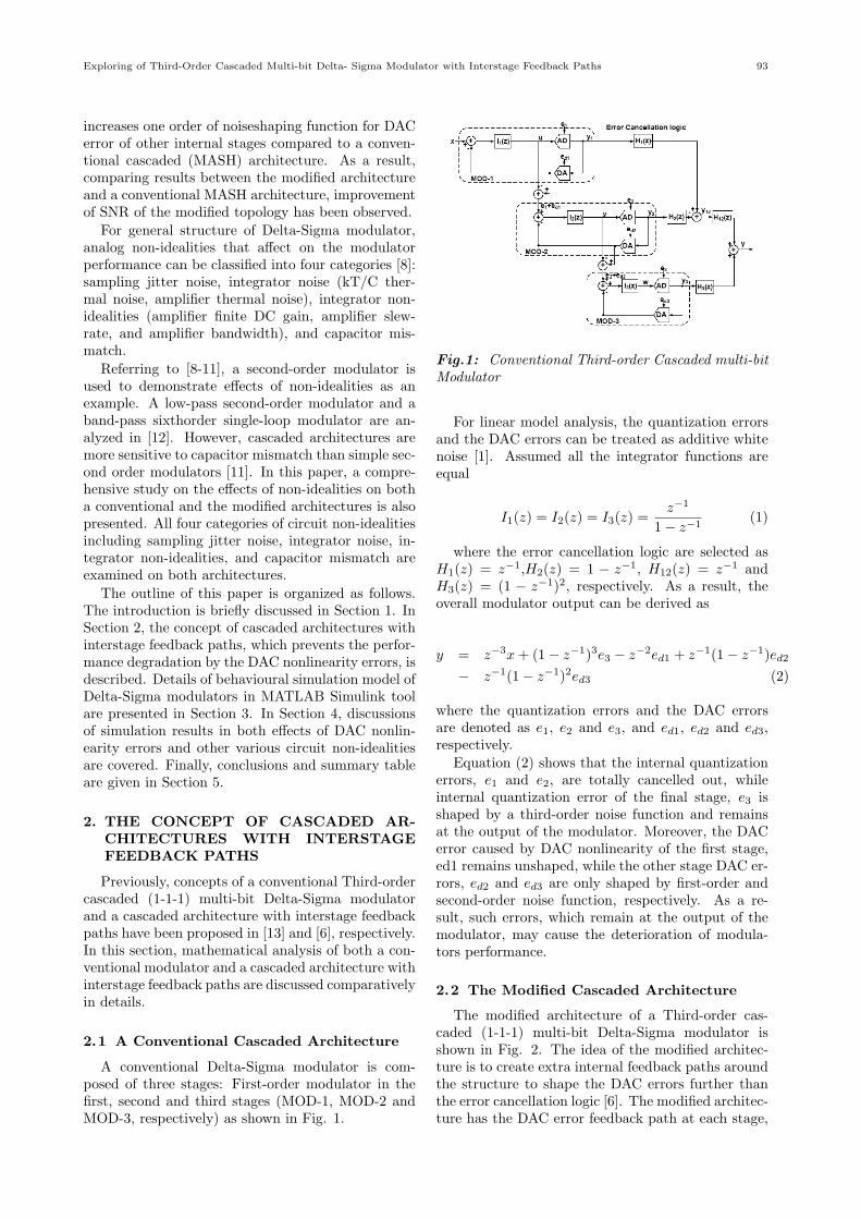
A conventional Delta-Sigma modulator is com-posed of three stages: First-order modulator in thefirst, second and third stages (MOD-1, MOD-2 andMOD-3, respectively) as shown in Fig. 1.
Fig.1: Conventional Third-order Cascaded multi-bitModulator
For linear model analysis, the quantization errorsand the DAC errors can be treated as additive whitenoise [1]. Assumed all the integrator functions areequal
I1(z) = I2(z) = I3(z) =z−1
1− z−1(1)
where the error cancellation logic are selected asH1(z) = z−1,H2(z) = 1 − z−1, H12(z) = z−1 andH3(z) = (1 − z−1)2, respectively. As a result, theoverall modulator output can be derived as
y = z−3x + (1− z−1)3e3 − z−2ed1 + z−1(1− z−1)ed2
− z−1(1− z−1)2ed3 (2)
where the quantization errors and the DAC errorsare denoted as e1, e2 and e3, and ed1, ed2 and ed3,respectively.
Equation (2) shows that the internal quantizationerrors, e1 and e2, are totally cancelled out, whileinternal quantization error of the final stage, e3 isshaped by a third-order noise function and remainsat the output of the modulator. Moreover, the DACerror caused by DAC nonlinearity of the first stage,ed1 remains unshaped, while the other stage DAC er-rors, ed2 and ed3 are only shaped by first-order andsecond-order noise function, respectively. As a re-sult, such errors, which remain at the output of themodulator, may cause the deterioration of modula-tors performance.
2.2 The Modified Cascaded Architecture
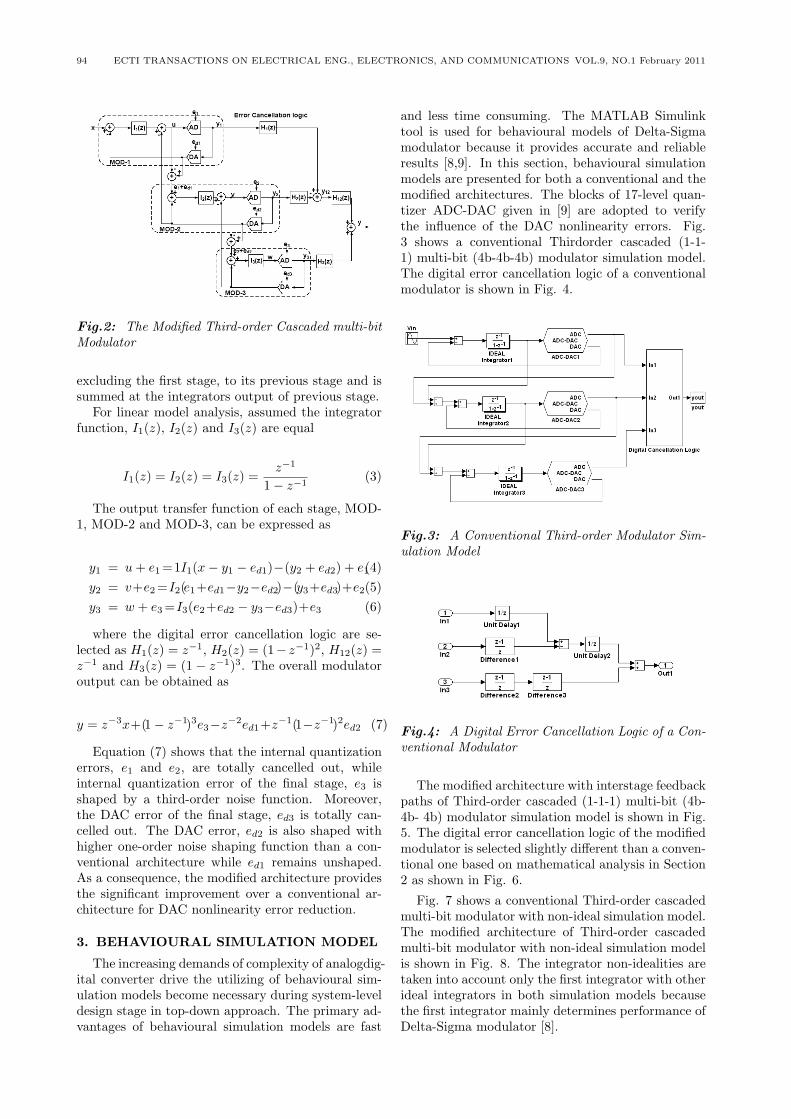
The modified architecture of a Third-order cas-caded (1-1-1) multi-bit Delta-Sigma modulator isshown in Fig. 2. The idea of the modified architec-ture is to create extra internal feedback paths aroundthe structure to shape the DAC errors further thanthe error cancellation logic [6]. The modified architec-ture has the DAC error feedback path at each stage,
94 ECTI TRANSACTIONS ON ELECTRICAL ENG., ELECTRONICS, AND COMMUNICATIONS VOL.9, NO.1 February 2011
Fig.2: The Modified Third-order Cascaded multi-bitModulator
excluding the first stage, to its previous stage and issummed at the integrators output of previous stage.
For linear model analysis, assumed the integratorfunction, I1(z), I2(z) and I3(z) are equal
I1(z) = I2(z) = I3(z) =z−1
1− z−1(3)
The output transfer function of each stage, MOD-1, MOD-2 and MOD-3, can be expressed as
y1 = u + e1 =1I1(x− y1 − ed1)−(y2 + ed2) + e1(4)y2 = v+e2 =I2(e1+ed1−y2−ed2)−(y3+ed3)+e2(5)y3 = w + e3 =I3(e2+ed2 − y3−ed3)+e3 (6)
where the digital error cancellation logic are se-lected as H1(z) = z−1, H2(z) = (1− z−1)2, H12(z) =z−1 and H3(z) = (1 − z−1)3. The overall modulatoroutput can be obtained as
y = z−3x+(1− z−1)3e3−z−2ed1+z−1(1−z−1)2ed2 (7)
Equation (7) shows that the internal quantizationerrors, e1 and e2, are totally cancelled out, whileinternal quantization error of the final stage, e3 isshaped by a third-order noise function. Moreover,the DAC error of the final stage, ed3 is totally can-celled out. The DAC error, ed2 is also shaped withhigher one-order noise shaping function than a con-ventional architecture while ed1 remains unshaped.As a consequence, the modified architecture providesthe significant improvement over a conventional ar-chitecture for DAC nonlinearity error reduction.
3. BEHAVIOURAL SIMULATION MODEL
The increasing demands of complexity of analogdig-ital converter drive the utilizing of behavioural sim-ulation models become necessary during system-leveldesign stage in top-down approach. The primary ad-vantages of behavioural simulation models are fast
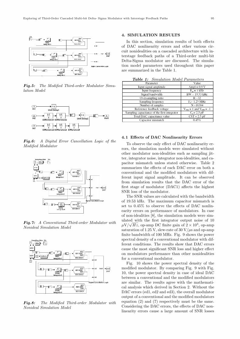
and less time consuming. The MATLAB Simulinktool is used for behavioural models of Delta-Sigmamodulator because it provides accurate and reliableresults [8,9]. In this section, behavioural simulationmodels are presented for both a conventional and themodified architectures. The blocks of 17-level quan-tizer ADC-DAC given in [9] are adopted to verifythe influence of the DAC nonlinearity errors. Fig.3 shows a conventional Thirdorder cascaded (1-1-1) multi-bit (4b-4b-4b) modulator simulation model.The digital error cancellation logic of a conventionalmodulator is shown in Fig. 4.
Fig.3: A Conventional Third-order Modulator Sim-ulation Model
Fig.4: A Digital Error Cancellation Logic of a Con-ventional Modulator
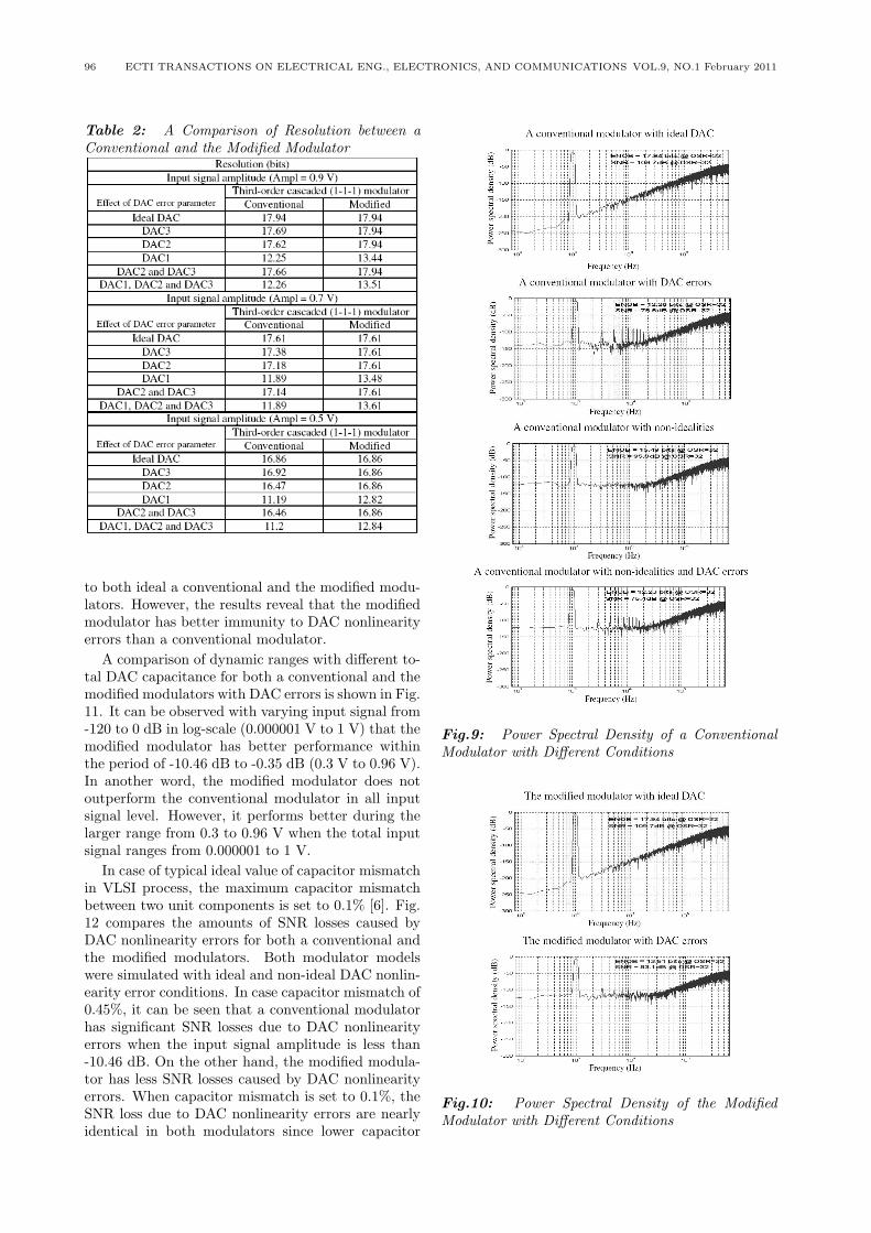
The modified architecture with interstage feedbackpaths of Third-order cascaded (1-1-1) multi-bit (4b-4b- 4b) modulator simulation model is shown in Fig.5. The digital error cancellation logic of the modifiedmodulator is selected slightly different than a conven-tional one based on mathematical analysis in Section2 as shown in Fig. 6.
Fig. 7 shows a conventional Third-order cascadedmulti-bit modulator with non-ideal simulation model.The modified architecture of Third-order cascadedmulti-bit modulator with non-ideal simulation modelis shown in Fig. 8. The integrator non-idealities aretaken into account only the first integrator with otherideal integrators in both simulation models becausethe first integrator mainly determines performance ofDelta-Sigma modulator [8].
Exploring of Third-Order Cascaded Multi-bit Delta- Sigma Modulator with Interstage Feedback Paths 95
Fig.5: The Modified Third-order Modulator Simu-lation Model
Fig.6: A Digital Error Cancellation Logic of theModified Modulator
Fig.7: A Conventional Third-order Modulator withNonideal Simulation Model
Fig.8: The Modified Third-order Modulator withNonideal Simulation Model
4. SIMULATION RESULTS
In this section, simulation results of both effectsof DAC nonlinearity errors and other various cir-cuit nonidealities on a cascaded architecture with in-terstage feedback paths of a Third-order multi-bitDelta-Sigma modulator are discussed. The simula-tion model parameters used throughout this paperare summarized in the Table 1.
Table 1: Simulation Model Parameters
4.1 Effects of DAC Nonlinearity Errors
To observe the only effect of DAC nonlinearity er-rors, the simulation models were simulated withoutother modulator non-idealities such as sampling jit-ter, integrator noise, integrator non-idealities, and ca-pacitor mismatch unless stated otherwise. Table 2summarizes the effects of each DAC error on both aconventional and the modified modulators with dif-ferent input signal amplitude. It can be observedfrom simulation results that the DAC error of thefirst stage of modulator (DAC1) affects the highestSNR loss of the modulator.
The SNR values are calculated with the bandwidthof 19.53 kHz. The maximum capacitor mismatch isset to 0.45% to observe the effects of DAC nonlin-earity errors on performance of modulators. In caseof non-idealities [8], the simulation models were sim-ulated with the first integrator output noise of 10µV/
√Hz, op-amp DC finite gain of 2× 10³, op-amp
saturation of 1.25 V, slew-rate of 30 V/µs and op-ampfinite bandwidth of 100 MHz. Fig. 9 shows the powerspectral density of a conventional modulator with dif-ferent conditions. The results show that DAC errorscause the most significant SNR loss and higher effecton modulators performance than other nonidealitiesfor a conventional modulator.
Fig. 10 shows the power spectral density of themodified modulator. By comparing Fig. 9 with Fig.10, the power spectral density in case of ideal DACbetween a conventional and the modified modulatorsare similar. The results agree with the mathemati-cal analysis which derived in Section 2. Without theDAC errors (ed1, ed2 and ed3), the overall modulatoroutput of a conventional and the modified modulatorsequation (2) and (7) respectively must be the same.Considering the DAC errors, the effects of DAC non-linearity errors cause a large amount of SNR losses
96 ECTI TRANSACTIONS ON ELECTRICAL ENG., ELECTRONICS, AND COMMUNICATIONS VOL.9, NO.1 February 2011
Table 2: A Comparison of Resolution between aConventional and the Modified Modulator
to both ideal a conventional and the modified modu-lators. However, the results reveal that the modifiedmodulator has better immunity to DAC nonlinearityerrors than a conventional modulator.
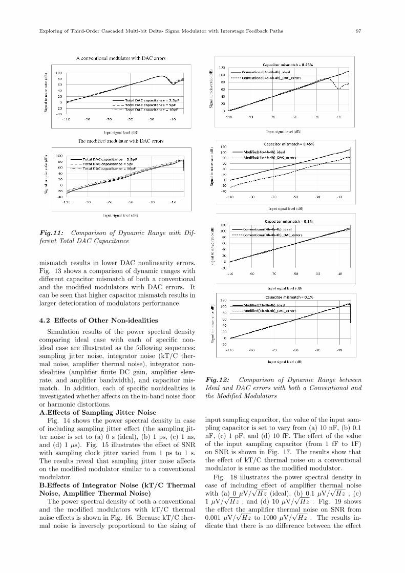
A comparison of dynamic ranges with different to-tal DAC capacitance for both a conventional and themodified modulators with DAC errors is shown in Fig.11. It can be observed with varying input signal from-120 to 0 dB in log-scale (0.000001 V to 1 V) that themodified modulator has better performance withinthe period of -10.46 dB to -0.35 dB (0.3 V to 0.96 V).In another word, the modified modulator does notoutperform the conventional modulator in all inputsignal level. However, it performs better during thelarger range from 0.3 to 0.96 V when the total inputsignal ranges from 0.000001 to 1 V.
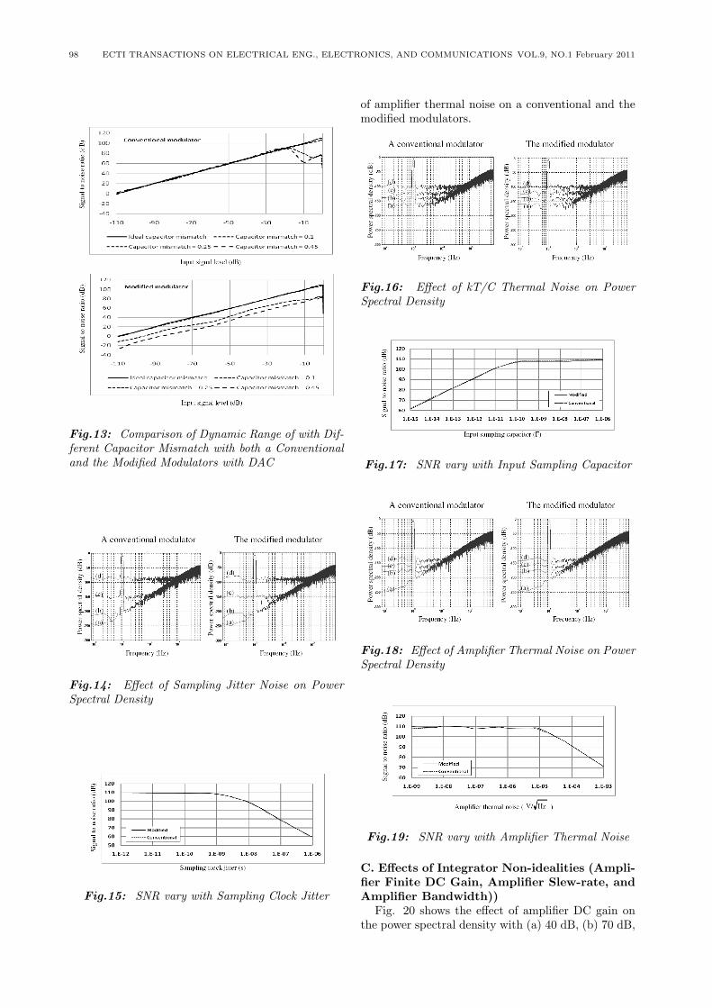
In case of typical ideal value of capacitor mismatchin VLSI process, the maximum capacitor mismatchbetween two unit components is set to 0.1% [6]. Fig.12 compares the amounts of SNR losses caused byDAC nonlinearity errors for both a conventional andthe modified modulators. Both modulator modelswere simulated with ideal and non-ideal DAC nonlin-earity error conditions. In case capacitor mismatch of0.45%, it can be seen that a conventional modulatorhas significant SNR losses due to DAC nonlinearityerrors when the input signal amplitude is less than-10.46 dB. On the other hand, the modified modula-tor has less SNR losses caused by DAC nonlinearityerrors. When capacitor mismatch is set to 0.1%, theSNR loss due to DAC nonlinearity errors are nearlyidentical in both modulators since lower capacitor
Fig.9: Power Spectral Density of a ConventionalModulator with Different Conditions
Fig.10: Power Spectral Density of the ModifiedModulator with Different Conditions
Exploring of Third-Order Cascaded Multi-bit Delta- Sigma Modulator with Interstage Feedback Paths 97
Fig.11: Comparison of Dynamic Range with Dif-ferent Total DAC Capacitance
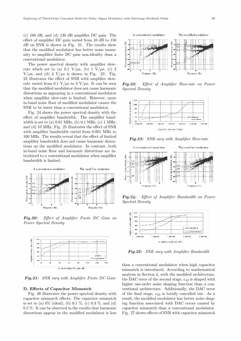
mismatch results in lower DAC nonlinearity errors.Fig. 13 shows a comparison of dynamic ranges withdifferent capacitor mismatch of both a conventionaland the modified modulators with DAC errors. Itcan be seen that higher capacitor mismatch results inlarger deterioration of modulators performance.
4.2 Effects of Other Non-idealities
Simulation results of the power spectral densitycomparing ideal case with each of specific non-ideal case are illustrated as the following sequences:sampling jitter noise, integrator noise (kT/C ther-mal noise, amplifier thermal noise), integrator non-idealities (amplifier finite DC gain, amplifier slew-rate, and amplifier bandwidth), and capacitor mis-match. In addition, each of specific nonidealities isinvestigated whether affects on the in-band noise flooror harmonic distortions.A.Effects of Sampling Jitter Noise
Fig. 14 shows the power spectral density in caseof including sampling jitter effect (the sampling jit-ter noise is set to (a) 0 s (ideal), (b) 1 ps, (c) 1 ns,and (d) 1 µs). Fig. 15 illustrates the effect of SNRwith sampling clock jitter varied from 1 ps to 1 s.The results reveal that sampling jitter noise affectson the modified modulator similar to a conventionalmodulator.B.Effects of Integrator Noise (kT/C ThermalNoise, Amplifier Thermal Noise)
The power spectral density of both a conventionaland the modified modulators with kT/C thermalnoise effects is shown in Fig. 16. Because kT/C ther-mal noise is inversely proportional to the sizing of
Fig.12: Comparison of Dynamic Range betweenIdeal and DAC errors with both a Conventional andthe Modified Modulators
input sampling capacitor, the value of the input sam-pling capacitor is set to vary from (a) 10 nF, (b) 0.1nF, (c) 1 pF, and (d) 10 fF. The effect of the valueof the input sampling capacitor (from 1 fF to 1F)on SNR is shown in Fig. 17. The results show thatthe effect of kT/C thermal noise on a conventionalmodulator is same as the modified modulator.
Fig. 18 illustrates the power spectral density incase of including effect of amplifier thermal noisewith (a) 0 µV/
√Hz (ideal), (b) 0.1 µV/
√Hz , (c)
1 µV/√
Hz , and (d) 10 µV/√
Hz . Fig. 19 showsthe effect the amplifier thermal noise on SNR from0.001 µV/
√Hz to 1000 µV/
√Hz . The results in-
dicate that there is no difference between the effect
98 ECTI TRANSACTIONS ON ELECTRICAL ENG., ELECTRONICS, AND COMMUNICATIONS VOL.9, NO.1 February 2011
Fig.13: Comparison of Dynamic Range of with Dif-ferent Capacitor Mismatch with both a Conventionaland the Modified Modulators with DAC
Fig.14: Effect of Sampling Jitter Noise on PowerSpectral Density
Fig.15: SNR vary with Sampling Clock Jitter
of amplifier thermal noise on a conventional and themodified modulators.
Fig.16: Effect of kT/C Thermal Noise on PowerSpectral Density
Fig.17: SNR vary with Input Sampling Capacitor
Fig.18: Effect of Amplifier Thermal Noise on PowerSpectral Density
Fig.19: SNR vary with Amplifier Thermal Noise
C. Effects of Integrator Non-idealities (Ampli-fier Finite DC Gain, Amplifier Slew-rate, andAmplifier Bandwidth))
Fig. 20 shows the effect of amplifier DC gain onthe power spectral density with (a) 40 dB, (b) 70 dB,
Exploring of Third-Order Cascaded Multi-bit Delta- Sigma Modulator with Interstage Feedback Paths 99
(c) 100 dB, and (d) 130 dB amplifier DC gain. Theeffect of amplifier DC gain varied from 10 dB to 150dB on SNR is shown in Fig. 21. The results showthat the modified modulator has better noise immu-nity to amplifier finite DC gain non-ideality than aconventional modulator.
The power spectral density with amplifier slew-rate which set to (a) 0.1 V/µs, (b) 1 V/µs, (c) 2V/µs, and (d) 3 V/µs is shown in Fig. 22. Fig.23 illustrates the effect of SNR with amplifier slew-rate varied from 0.1 V/µs to 3 V/µs. It can be seenthat the modified modulator does not cause harmonicdistortions as appearing in a conventional modulatorwhen amplifier slew-rate is limited. However, morein-band noise floor of modified modulator causes theSNR to be lower than a conventional modulator.
Fig. 24 shows the power spectral density with theeffect of amplifier bandwidth. The amplifier band-width is set to (a) 0.01 MHz, (b) 0.1 MHz, (c) 1 MHz,and (d) 10 MHz. Fig. 25 illustrates the effect of SNRwith amplifier bandwidth varied from 0.001 MHz to100 MHz. The results reveal that the effect of limitedamplifier bandwidth does not cause harmonic distor-tions on the modified modulator. In contrast, bothin-band noise floor and harmonic distortions are in-troduced to a conventional modulator when amplifierbandwidth is limited.
Fig.20: Effect of Amplifier Finite DC Gain onPower Spectral Density
Fig.21: SNR vary with Amplifier Finite DC Gain
D. Effects of Capacitor MismatchFig. 26 illustrates the power spectral density with
capacitor mismatch effects. The capacitor mismatchis set to (a) 0% (ideal), (b) 0.1 %, (c) 0.3 %, and (d)0.5 %. It can be observed in the results that harmonicdistortions appear in the modified modulator is less
Fig.22: Effect of Amplifier Slew-rate on PowerSpectral Density
Fig.23: SNR vary with Amplifier Slew-rate
Fig.24: Effect of Amplifier Bandwidth on PowerSpectral Density
Fig.25: SNR vary with Amplifier Bandwidth
than a conventional modulator when high capacitormismatch is introduced. According to mathematicalanalysis in Section 2, with the modified architecture,the DAC error of the second stage, ed2 is shaped withhigher one-order noise shaping function than a con-ventional architecture. Additionally, the DAC errorof the final stage, ed3 is totally cancelled out. As aresult, the modified modulator has better noise shap-ing function associated with DAC errors caused bycapacitor mismatch than a conventional modulator.Fig. 27 shows effects of SNR with capacitor mismatch
100 ECTI TRANSACTIONS ON ELECTRICAL ENG., ELECTRONICS, AND COMMUNICATIONS VOL.9, NO.1 February 2011
varied from 0% to 0.5% (typical standard VLSI pro-cess). The result shows that the modified modula-tor has better SNR than a conventional modulator.In other words, the modified modulator has betterimmunity to DAC nonlinearity errors than a conven-tional modulator when including effects of DAC er-rors caused by capacitor mismatch.
Fig.26: Effect of Capacitor Mismatch on PowerSpectral Density
Fig.27: SNR vary with Capacitor Mismatch
5. CONCLUSION
A study of non-ideal effects on special architec-ture allow us to design carefully regarding this con-cerns and precisely estimate specifications of particu-lar modulator basic building blocks at the early stageof design without deteriorated performance of mod-ulator caused by nonidealities. In this paper, wehave investigated characteristic of Third-order cas-caded (1-1-1) multi-bit (4b-4b-4b) Delta-Sigma mod-ulator with interstage feedback paths in behaviouralsimulation model. The concept of DAC nonlinearityerror reduction technique for a third-order cascadedmulti-bit Delta-Sigma modulator is presented. Be-havioural simulations have been also performed forDAC errors as well as other analog non-idealities inboth ideal and non-ideal cases.
Initially, analysis effects of DAC nonlinearity er-rors caused large degradation of modulator perfor-mance are studied. DAC nonlinearity problems ineach stage of a conventional and the modified mod-ulators have been analyzed. Behavioural simulationresults show that, among modulator non-idealities,the most deterioration of modulators performance iscaused by DAC nonlinearity errors. Moreover, theresults reveal that the DAC error caused by the first
stage of the cascaded modulator affects the highestSNR loss of the modulator. The effect of both totalDAC capacitance and capacitor mismatch parame-ters to dynamic range of modulators has also beenanalyzed.
Finally, we demonstrate a comprehensive analy-sis of other analog non-ideal effects whether on thein-band noise floor or harmonic distortions of third-order cascaded modulator with interstage feedbackpaths. Table 3 summarizes the effects (the in-bandnoise floor and harmonic distortions) of each of spe-cific non-idealities on both modulator architectures.It can be concluded from simulation results that non-ideal effects of amplifier DC finite gain, slew-rate, andbandwidth cause different inband noise floor and har-monic distortion results on both a conventional andthe modified modulators.
Table 3: Summary of Non-ideal Effects
6. ACKNOWLEDGEMENT
This work was partially supported and funded byTGIST (Thailand graduate institute of science andtechnology), NSTDA (National Science and Technol-ogy Development Agency), with contact No. TGIST01-52- 068.
References
[1] R. L. Carley, R. Schreier and G. C. Temes,“Delta- Sigma ADCs with multibit internal con-verters,” Delta- Sigma Data Converters: The-ory, Design, and Simulation, IEEE Press NewYork, NY, 1997.
[2] J. C. Candy, “An overview of basic concepts,”Delta- Sigma Data Converters: Theory, Design,and Simulation, IEEE Press New York, NY,1997.
[3] T. C. Leslie and B. Singh, “An improved sigma-delta modulator architecture,” IEEE Interna-tional Symposium on Circuits and Systems (IS-CAS), Vol.1, pp.372-375, 1990.
[4] S. Lindfors and K. Halonen, “Two-step quantiza-tion in multibit ∆Σ modulators,” IEEE Transac-tions on Circuits and Systems II, Vol.48, pp.171-176, 2001.

Exploring of Third-Order Cascaded Multi-bit Delta- Sigma Modulator with Interstage Feedback Paths 101
[5] M. C. Ramesh and K. S. Chao, “Pipelined sigma-delta modulators with interstage scaling,” 42ndMidwest Symposium on Circuits and Systems(MWSCAS), vol. 1, pp. 39-42, 1999.
[6] C. H. Su and K. S. Chao, “A fourth-ordercascaded sigma-delta modulator with DAC er-ror cancellation technique,” The 2002 45thMidwest Symposium on Circuits and Systems(MWSCAS-2002), Vol.1, pp.132- 135, 2002.
[7] L. Fang and K. S. Chao, “A multi-bit sigma-delta modulator with interstage feedback,” Pro-ceedings of the 1998 IEEE International Sym-posium on Circuits and Systems (ISCAS 98),Vol.1, pp.583-586, 1998.
[8] S. Brigati et al, “Modeling sigma-delta modu-lator non-idealities in Simulink,” Proceedings ofthe 1999 IEEE International Symposium on Cir-cuits and Systems (ISCAS 99), Vol.2, pp.384-387, 1999.
[9] A. Fornasari, P. Malcovati and F. Maloberti,“Improved modeling of sigma-delta modulatornonidealities in Simulink,” IEEE InternationalSymposium on Circuits and Systems (ISCAS2005), Vol.6, pp.5982-5985, 2005.
[10] H. Zare-Hoseini, I. Kale and O. Shoaei, “Mod-eling of switched-capacitor delta-sigma modula-tors in simulink,” IEEE Transactions on Instru-mentation and Measurement, Vol.54, pp.1646-1654, 2005.
[11] W. Koe and J. Zhang, “Understanding the effectof circuit non-idealities on sigma-delta modula-tor,” Proceedings of the 2002 IEEE InternationalWorkshop on Behavioral Modeling and Simula-tion (BMAS 2002), pp.94-101, 2002
[12] P. Malcovati et al., “Behavioral modelingof switched-capacitor sigma-delta modulators,”IEEE Transactions on Circuits and Systems I,Vol.50, pp.352-364, 2003.
[13] Y. Matsuya et al., “A 16-bit oversampling A-to-D conversion technology using triple integrationnoise shaping,” IEEE Journal of Solid-State Cir-cuits, Vol. 22, pp.921-929, 1987.
[14] M. Rebeschini, “The design of cascaded ∆ΣADCs,” Delta-Sigma Data Converters: Theory,Design, and Simulation, IEEE Press New York,NY, 1997.
Sarayut Amornwongpeeti recievedhis B.Eng. degree in Electrical Engi-neering from King Mongkuts Instituteof Technology Lardkrabang, Bangkok,Thailand, and his M.Eng. degree inMicroelectronics from Asian Institute ofTechnology, Pathumtani, Thailand in2007, and 2010, respectively. From2009 to 2010, he was a research studentat Thailand IC design and InnovationLaboratory (TIDI), National Electron-
ics and Computer Technology Center (NECTEC).
Mongkol Ekpanyapong is an Assis-tant Professor at the department of Mi-croelectronics and Embedded Systems,Asian Institute of Technology. He re-ceived his B.Eng. degree from Chula-longkorn Univerisity, Thailand in 1997,his M.Eng. degree from Asian Insti-tute of Technology, Thailand in 2000, hisM.Sc., and his Ph.D. from Georgia In-stitute of Technology, USA, in 2003, and2006 respectively. From 2006 to 2009, he
was a Senior Computer Architect at Intel Corporation, USA,Core 2 Architecture design team. His research focus is in thearea of VLSI design, physical design automation, microarchi-tecture, compiler, GPGPU, and Embedded Systems.
Chumnarn Punyasai (M10) was bornin Yasothon, Thailand on May 19, 1967.He received a B.SC. degree with secondclass honor in Physics from Khon KaenUniversity, Thailand and an MS degreein Computer Engineering from Univer-sity of Southwestern Louisiana, USA in1989 and 1992 respectively. He has beenworking as a researcher at National Elec-tronics and Computer Technology Cen-ter (NECTEC) since 1993. He has in-
volved several IC design R&D and educational programs atNECTEC. His interests include low power and mixed signalVLSI design, FPGA design, logic synthesis and test. Cur-rently, He also teaches a VLSI design related course at AsianInstitute of Technology, and Bangkok University, Thailand.