exploring microdischarges for portable sensing...
TRANSCRIPT

REVIEW
Exploring microdischarges for portable sensing applications
Y. B. Gianchandani & S. A. Wright & C. K. Eun &
C. G. Wilson & B. Mitra
Received: 30 May 2009 /Revised: 20 July 2009 /Accepted: 23 July 2009 /Published online: 12 August 2009# Springer-Verlag 2009
Abstract This paper describes the use of microdischargesas transducing elements in sensors and detectors. Chemicaland physical sensing of gases, chemical sensing of liquids,and radiation detection are described. These applicationsare explored from the perspective of their use in portablemicrosystems, with emphasis on compactness, powerconsumption, the ability to operate at or near atmosphericpressure (to reduce pumping challenges), and the ability tooperate in an air ambient (to reduce the need for reservoirsof carrier gases). Manufacturing methods and performanceresults are described for selected examples.
Keywords Plasma . Discharge . Chemical . Radiation .
Pressure
Introduction
In the past decade, microplasmas, or more generallymicrodischarges, have been investigated for their funda-
mental properties, and have been explored for uses insensing applications. The intent, in most cases, is toincorporate microdischarge-based devices into portable,battery-powered analytical systems. Such systems alsooffer the potential benefits of requiring smaller samples,requiring smaller reagent volumes, requiring low power,and being less expensive to manufacture. Microdischarges,in such systems, can be used directly as transducers thatproduce electrical signals, or as a means of fractionating,ionizing, and exciting species, which are then analyzed byanother component.
One promising application area for microdischarge-baseddevices is chemical sensing. Recent years have witnessed anincreasing interest in miniaturized and portable systems forgas sensing, with applications ranging from environmentalmonitoring to homeland security. The emission spectrum of adischarge arises from spontaneous emission due to relaxationof excited chemical species to their ground states. A singleobservation can provide information regarding the composi-tion of the ambient gas mixture. With modifications, emissionspectroscopy of microdischarges can be extended to liquid-phase ambients.
There are other promising application areas for micro-discharges as well. Conventionally, gas discharges havebeen used in the detection of radiation, as in Geigercounters and proportional counters. Miniaturized versionsof these detectors utilize microdischarges. Recent work hasalso explored microdischarge-based pressure sensors forhigh-temperature environments: the relatively high electronand ion temperatures in microdischarges are less affectedby the ambient temperature than are the transducingmaterials of most other sensors.
Microdischarges are similar to conventional dischargesat larger scales in many ways, but have some importantdistinctions. As the distance between electrodes is de-
Y. B. Gianchandani (*) : S. A. Wright : C. K. EunCenter for Wireless Integrated Microsystems,University of Michigan,EECS Building, 1301 Beal Ave,Ann Arbor, MI 48109-2122, USAe-mail: [email protected]
C. G. WilsonInstitute for Micromanufacturing,Louisiana Tech University,911 Hergot Avenue,Ruston, LA 71272, USA
B. MitraDepartment of Electrical Engineering and Computer Engineering,Rutgers University, 94 Brett Road,Piscataway, NJ 08854-8058, USA
Anal Bioanal Chem (2009) 395:559–575DOI 10.1007/s00216-009-3011-6

creased, the pressure at which lower currents and stabledischarges exist is increased, up to and exceeding atmo-spheric pressure. Additionally, the relatively large ratio ofsurface area to discharge volume can make wall interactionsmore prominent. In DC-powered microdischarges, with theionization dominated by secondary electrons, the glowregion is proximal to the cathode and may overlap the high-field region. Another consequence of miniaturization is thatvery high power densities can be achieved withoutrequiring high power: whereas conventional plasmas mayoperate at 10–500 mW/cm2, microdischarges can beoperated at 1–10 W/cm2. Electron temperatures can be alsorelatively high, reaching 5–6 eV in microdischarges withsmall percentages of very high energy beam electrons. Thedistinctions between conventional and microscale dis-charges are reviewed in [1].
This paper explores how microdischarges can be used asa transduction element in different domains. “Gas-phasesensing” describes gas-phase sensing of chemical species andpressure; a brief review of different types of microdischargesis also included. “Liquid-phase sensing” describesmicrodischarge-based transducers for liquid-phase applica-tions. “Radiation detection” describes microdischarges in thecontext of radiation detection. (Microdischarges used fordisplay, surface treatment, destruction of gas pollutants,propulsion, in situ etching and deposition, sterilization, dentalapplications, and microwelding are beyond the scope of thispaper.) All microdischarge-based transducers that arereviewed have some features with submillimeter dimensions,and are typically microfabricated. To the extent possible, allapplications are explored from the perspective of micro-systems, with emphasis on compactness and power con-sumption; the ability to operate at or near atmosphericpressure (to reduce pumping challenges); and the ability tooperate in an air ambient (to reduce the need for a reservoir ofcarrier fluid).
Gas-phase sensing
Microdischarge-based gas-phase sensing has been performedthrough optical emission spectroscopy (as noted previously),or by other means such as mass or ion-mobility spectrometry.In contrast with conventional gas sensors, which depend onthe absorption of selected analytes, microdischarge-basedtransducers are typically amenable to rapid and concurrentsensing of multiple species, and are less sensitive to thefabrication process and operating temperatures [2, 3].
A variety of DC- and RF-powered microdischarges havebeen explored in gas-phase microdischarge-based trans-ducers, and have been reviewed in several papers [2–7].RF-powered transducers utilize a dielectric layer betweenthe electrodes and the plasma region, which prevents
sputtering of the electrodes by bombarding positive ionsto increase the electrode lifetime and minimize spectralinterference. Additionally, RF-powered microdischarges donot heat the electrodes to the same extent as DC-poweredmicrodischarges. DC-powered transducers require lessexternal hardware for operation, such as a simpler powersource. The lifetime of DC-powered transducers can beextended by utilizing pulsed discharge operation.
DC glow discharges in inert gases at atmosphericpressure have been used for optical emission spectroscopy,and have been attached at the ends of gas chromatographs(GCs) for decades [8]. GCs are one of the most powerfulanalytical instruments available today for the separation andidentification of mixtures of gases. After separation,sensing or detection can be performed by a variety ofmeans, ranging from mass spectrometry to simple thermalflow sensors. Recent efforts to miniaturize GCs [9, 10]present opportunities for integration with microdischarge-based transducers. An early paper describes a microplasmamass spectrometer coupled to a GC for halogen detection[11]. A review paper detailing the use of microdischarge-based transducers with GCs has also been published [12].
Several different varieties of microdischarges have beenused to determine gas composition and pressure. Theseinclude the miniature inductively coupled plasma (ICP),microwave-induced plasma (MIP), capacitively coupledplasma (CCP), dielectric barrier discharge (DBD), micro-hollow cathode discharge (MHCD), planar DC microplasma,pulsed microarc, three-electrode microdischarge, arc-glowhybrid microdischarge, and multicathode pulsed DC micro-discharge. A brief explanation of each follows.
Inductively coupled plasmas
ICPs are used in laboratory-scale devices for atomicemission spectroscopy. They require large volumes, largeamounts of argon, water cooling, and have high powerrequirements of 1–2 kW. They typically generate plasmas atatmospheric pressure within a quartz tube with a helical coilwound around the tube providing energy at frequencies of10–60 MHz. To allow for portable sensing in the field,several research groups have developed miniature ICPgenerators and have attached them to both Fabry-Perotinterferometers and atomic emission spectrometers. ICPsdiffer from CCPs. The electric field in CCPs is parallel tothe electrodes and accelerates ions from the plasma into thechamber walls, which heat and sputter the chamber. Theelectric field in ICPs is perpendicular to the electrodes, andthus does not accelerate the ions into the chamber walls andallows more power for ionization and excitation.
Miniaturized ICP (mICP) devices were developed byHopwood’s group [13]. The devices were microfabricatedwith planar load coils, with coil diameters of 5, 10, and
560 Y.B. Gianchandani et al.

15 mm, to provide the inductive field. The devices operatedat pressures between 0.1 and 10 Torr, and the optimumfrequency for plasma generation was found to be 460 MHz.The electron temperature in the mICPs was found to bebetween 3 and 9 eV. These devices were modified to operateat 450 MHz in both argon and air [14]. They required 1.5 Wfor initiation, although they could be sustained with 350 mW.The mICPs were later operated in argon with increasedplasma power and a silicon photodiode emission detector[15]. The limit of detection for SO2 was 190 ppb using the469.5 nm sulfur emission line with 3.5 W of input power.The most intense emissions existed adjacent to the planarcoil beyond the plasma sheath, and this region wasspecifically observed to obtain the detection limit. Thedetection limit was later improved to 45 ppb in an argonenvironment and a model was developed to calculate theargon density, electron temperature, and SO2 excitation rate[16]. However, the transducer still required a reduced-pressure environment.
Microwave-induced plasmas
Microwave-induced plasmas operating with frequencies inthe gigahertz range have been used in optical emissionspectrometry for decades and have recently undergoneminiaturization. These plasmas exhibit lower gas temper-atures than ICPs as the energy delivered to gas atoms andions is lower than the energy delivered to electrons at thesehigh frequencies.
Broekaert’s group [17] reported microwave-inducedmicroplasmas created in a dielectric channel with an externalelectrode at atmospheric pressure. Two quartz plates, 1 mm×30 mm×90 mm, were bonded together creating a channelbetween them with dimensions of 0.9 mm×1 mm×90 mm.The microstrip electrode consisted of a small strip over thegas channel and was electroplated onto the structure. A 2.45-GHz microwave signal was applied with an input power of10–40 W. Atomic emission spectroscopy was used with amonochromator to detect gaseous species and the 253.7 nmmercury emission line was used to obtain a detection limit of0.05 µg/l [18]. A modified structure used sapphire substrates30 mm in length and a helium ambient with an input powerof 5–30 W. The transducer was used to break downhalogenated hydrocarbons and detected HCCl3 through the912.1 nm chlorine emission line [19]. The configuration wasfurther modified in a smaller device creating a microplasmajet, which extended 2 mm from the channel for enhanceddetection [20]. With use of 30 W and an argon ambient, adetection limit of 0.01 µg/l was obtained using the 253.7 nmmercury emission line. However, an air cooler was used withthis device. The channel was later reduced to have a 600 µmin diameter, and sulfur was detected at 0.1 µg/l [21]. Thesedevices utilized external sources for microplasma ignition.
A coaxial structure was used to create a microwavemicroplasma jet, which extended 4 mm from the end of thecoaxial line at atmospheric pressure [22]. The microplasmawas created with a 2.45 GHz source and could be maintainedwith 2 W of power, after it had been initiated with around10 W. The device operated in both argon and helium for over30 h. It was used as a microdischarge-based transducer and the912.1 nm chlorine emission line was used to detect HCCl3,producing a detection limit of 66 ppb.
Iza and Hopwood [23] developed a microwave split-ringresonator plasma source for spectroscopic applications thatoperated at pressures from 50 mTorr to atmosphericpressure in argon and air. The initial resonator had a gapin which the microplasma was formed of 500 µm, aresonant frequency of 900 MHz, and a quality factor Q=355. A modified resonator had a gap of 25 µm, a resonantfrequency of 895 MHz, and obtained a quality factor Q=142 [24–26]. At the resonant frequency, a voltage drop of390 V was created across the 25-µm gap. This was highenough to initiate a microplasma at atmospheric pressure,indicating a self-igniting microplasma. The resonators con-sumed 3 Wof power at atmospheric pressure, and operated atthis pressure continuously for 50 h without significantelectrode erosion. Carbon deposition was the noticeableresult. The device achieved a detection limit of 200 ppb forSO2 in argon at a reduced pressure of 2.5 Torr [25].
Capacitively coupled microplasmas
Capacitively coupled microplasmas have two dielectric layersin contact with the plasma and typically utilize the traditional13.56-MHz excitation frequency. They benefit from longlifetimes as the dielectric layers separate the plasma from theexternal electrodes, which typically have a simple geometry.Capacitively coupled microplasmas have been operated inhelium at atmospheric pressure, which eliminates the need forvacuum components but still requires an external gas source.
A capacitively coupled transducer was developed forabsorption and emission analysis by Liang and Blades [27]and was later miniaturized in a fused-silica chip foratmospheric pressure operation [28]. The chip createdmicroplasmas in a channel, confined by two quartzsubstrates. This channel was formed in the bottomsubstrate, 200–500 µm deep and 10 mm long, and the topsubstrate served as a lid. A pair of electrodes was used, oneon the outer surface of each quartz substrate, forming acapacitively coupled discharge in the channel betweenthem. Helium was used as the carrier gas, and the dischargewas sustained with the application of 5–25 W of power at13.56 MHz. When gas flowed through the channel withsufficient velocity, a microplasma jet was formed and it wasanalyzed using emission spectroscopy. Spectral measure-ments indicated the presence of OH, NH, N2, N2
+, and
Exploring microdischarges for portable sensing applications 561
helium. Yoshiki and Horike [29] reported a similar device,with the addition of an on-chip matching network tomaximize power transfer. This group later reported capac-itively coupled microplasmas in ceramic tubes and in combelectrode configurations, as well as a capacitively coupleddischarge variation that they described as “ICP-type” [30].
A so-called stabilized capacitively coupled 27 MHzmicroplasma was created in helium at atmospheric pressureby Gross et al. [31]. The device used a silica tube with a0.75-mm outer diameter and a 0.53-mm inner diameter asthe dielectric, which was surrounded by two annularelectrodes. Liquid cooling was used to prevent overheatingand melting. The microdischarge-based transducer andaccompanying spectrometer was attached to a GC. Seven-teen different compounds were analyzed by examining theH2, O2, N2, argon, and CO2 emission lines.
Dielectric barrier discharges
DBDs are similar to capacitively coupled microplasmas asthey have at least one dielectric layer in contact with thedischarge, as opposed to an electrode. However, they operateat much lower frequencies, from a few hertz to severalmegahertz, usually in the kilohertz range. Typically, the poweris applied by a square, sinusoidal, or pulsed high-voltagewaveform. DBDs are highly transient, low-temperature,nonequilibrium discharges, formed from electrons of highmean energy and exist over a broad range of pressures [32,33]. DBDs differ from other microscale high-frequencydischarges in that they accumulate charge on the dielectriclayer, known as memory voltage formation, which decreasesthe breakdown voltage of the gas. This effect is not seen atfrequencies higher than those at which DBDs operate.Additionally, DBDs do not sputter the discharge electrodes,as the electrodes are covered by a dielectric layer. Thedischarges are traditionally created in helium and argonenvironments, and are employed in flat-panel plasma dis-plays, in the treatment of surfaces, as mercury-free radiationsources, in plasma chemistry, and in excimer lamps.
Two different configurations are used in DBDs. The“volume discharge” configuration consists of two parallelelectrodes separated by the gas medium and a dielectriclayer, and the discharge is created in the gas medium. Incontrast, the “surface discharge” configuration has anelectrode on one side of a dielectric layer and a metallicfeature on the reverse side of the dielectric, and thedischarge is created around this feature. Both variationscan operate at atmospheric pressure and consist of arclikedischarge pulses that are approximately 10 ns in duration.
Cylindrical DBDs (C-DBDs) are created in a variation ofthe DBD configuration. They are formed in cylindricaldielectric alumina or silica tubes with electrodes wrappedaround the tubes. This essentially uses two dielectric layers
between the electrodes and confines the discharges betweenthe electrodes along the tube length. These discharges are usedas UV and VUV emission sources in pure argon, argon-N2,and argon-air mixtures at pressures up to 500 Torr [34].
Niemax’s group [35–37] reported low-pressure DBDs inhelium and argon and used them with diode laser atomicabsorption spectrometry for the detection of halogens innoble gas mixtures. The discharges consumed 0.5–1 W ofpower at frequencies of 5–20 kHz, at pressures of 4–120 Torr. Collinear beams of light from semiconductordiode lasers were passed through the DBDs, and weremeasured individually with photodiodes. This DBD con-figuration was used with a GC to detect halogenated andsulfured hydrocarbons through the elements fluorine,chlorine, bromine, iodine, and sulfur [38]. However, theuse of absorption spectrometry necessitated low operatingpressures and an inert ambient, which is challenging toprovide in the context of portable applications.
Another application of DBDs was atomizing hydride-forming elements for their detection using an atomicabsorption spectrometer as demonstrated by Zhu et al.DBD-based devices were used to detect arsenic [39],selenium, antimony, and tin at atmospheric pressure withan argon carrier gas [40]. A sine-wave voltage of 3.5–4 kVwas used at a frequency of 20.3 kHz. Selenium, antimony, andtin had detection limits of 0.6, 13, and 10.6 µg/l, respectively.A new DBD atomizer was designed for use in atomicfluorescence spectrometry and was placed between a hollowcathode lamp and a photomultiplier tube detector [41, 42].The device had a cylindrical configuration consisting of twoconcentric quartz tubes. The discharge was created in thecenter tube and a shield gas was contained in the outer tube.The detection limits for arsenic, selenium, tin, and lead were0.04, 0.08, 0.11, and 0.27 µg/l, respectively.
A C-DBD capable of functioning at atmosphericpressure was developed as a microdischarge-based devicefor vapor sensing by Guchardi and Hauser [43]. A fused-silica capillary was used as the dielectric layer and twocylindrical electrodes separated from each other by 12 mmalong the length of the capillary were used to capacitivelycouple energy into the tube. An AC voltage was used at afrequency of 20 kHz and 20 kV for a total of 8 W of power.Helium and argon were used as carrier gases and opticalemissions were recorded with an external spectrometer fordetection. Atomic emissions were examined andmetal mercuryvapor was detected with a detection limit of 200 ppb.Additionally, CO2, CH4, and ethanol vapors were detectedusing the 385.2 nm emission line, attributed to carbon, and thedetection limits were found to be 90, 30, and 33 ppb,respectively. The device was operated for over 1 monthwithout renewing the capillary tubing. This C-DBD was laterused with an optical emission detector and coupled to a GC todetect inorganic [44] and organic [45, 46] compounds.
562 Y.B. Gianchandani et al.

Another C-DBD design was utilized as an ionizationsource for an ion-mobility spectrometer at atmosphericpressure by Michels et al. [47]. Although the structure ofthis device was similar to that of the last one (i.e., having adielectric capillary surrounded by two ring electrodes), itdiffered in that a microplasma jet was created by flowing ahelium buffer gas through the capillary. The electrodes werespaced 12 mm apart and the closer of the two was 2 mmfrom the microplasma jet end of the capillary tube. Avoltage of 5.5 kV was applied at a frequency of 33 kHz.Coupling the microdischarge to an ion-mobility spectrom-eter resulted in a detection limit of 55 ppb of 2-heptanone,and a minimum detection limit of 5 ppb.
Microhollow cathode discharges
Microdischarges created in cylindrical hollow cathodegeometries, such as the circular metal-insulator-metalsandwich structure, are referred to as microhollow cathodedischarges (MHCDs) [48]. In these structures, the dis-charges are spatially confined within the perforationthrough the structure, typically 10–500 µm in diameter.The two metal layers serve as separate anode and cathodeelectrodes, and the insulating layer thickness defines thedischarge gap spacing. They operate at low and atmospher-ic pressures and can be formed using DC and AC voltages.MHCDs have high ionization efficiency, and the mecha-nisms of ionization include pendulum motion of electronsin the cathode perforation, secondary electron emissionfrom the cathode, and Penning ionization. Traditionally, theterm “hollow cathode” refers to a mode of operation inwhich the sustaining voltage drops as the current increases(i.e., the hollow cathode mode), but MHCDs commonlyoperate as normal or abnormal glow discharges. As a result,MHCDs have also been referred to as microstructureelectrode discharges [36] and microdischarges [49].
Schoenbach et al. [50, 51] originally used the spectraproduced as excimer light sources, designed to emit light atcertain frequencies. In addition to the use of these devicesin chemical sensors and light sources, research on MHCDswas motivated by uses in applications including instantlyactivated reflectors and absorbers for electromagneticradiation in industrial applications, surface treatments,thin-film depositions, remediation and detoxification ofgaseous pollutions, and gas lasers [48, 51].
A microdischarge-based transducer was created usingMHCDs by Miclea et al. [36], which used DC voltages andhelium and argon ambients at atmospheric pressure todetect chlorine and fluorine. The device used more than2 W of power. An external spectrometer was used to detectemissions. The device had 30-µm-thick platinum electrodeswith Al2O3 as an insulator. The perforation through thesandwich structure had a diameter of 100 µm and the
electrodes were spaced 200 µm apart. CCl2F2 and CHClF2were decomposed and detected with a detection limit of20 ppb for chlorine and fluorine using the 912.1 nmchlorine emission line or the 739.9 nm fluorine emissionline. The devices were able to operate for more than 1 weekin helium using a ceramic insulator and electrodes madefrom materials with low sputtering rates such as platinumand tungsten. This device was later used to detect ferroceneusing the 371.9 and 344.1 nm emission lines of iron, with adetection limit of 500 ppb [52]. This device, with slightlydifferent dimensions, was used with a GC [7, 12]. MHCDswere investigated between 40 Torr and atmospheric pressureto determine the gas temperature and electron density usingabsorption and emission spectroscopy [52]. An atmosphericpressure helium MHCD jet was also developed as a miniatureion source for mass spectrometry by Miclea et al. [53].
A subsequent effort by Eden’s group [54, 55] utilizedMHCDs for display applications. Arrays of microplasmaswere fabricated with apertures of 80 µm×380 µm usingceramic tape as the insulating layer between electrodes.Xenon was excited between 45 and 480 nm to produce blueemissions, indicating the potential for applications inchemical sensing.
Planar DC microplasmas
Planar DC microdischarges are created above thin-filmelectrodes, typically patterned on a dielectric layer or glasssubstrate. The planar microdischarges are similar toMHCDs, but differ in that they are not confined in acircular cavity. Rather, they expand between electrodes; theexpansion depends on the applied voltage and pressure.This also allows for multiple path lengths that aresimultaneously available between electrodes. This makesthe discharge gap a variable and permits a low breakdownvoltage to be sustained, even as the pressure changes fromthe value that favors the minimum electrode spacing asdiscussed in [56, 57]. However, the microdischarges havebeen confined in chambers and channels when necessary.These microdischarges are commonly created using DCbiases at pressures as high as 1 atm. Devices utilizingplanar microdischarges can be fabricated using traditionalIC microfabrication techniques on two-dimensional chips,making them attractive from a fabrication standpoint.
One of the first reported microdischarge-based trans-ducers was developed by Manz’s group [58] and utilizedplanar DC microplasmas in helium contained within achamber. An external spectrometer was used for detection.The planar electrodes were patterned from chromium andgold deposited on a flat glass chip. Chambers of variousgeometric dimensions and volumes, from 50 to 450 nl,were created by wet etching a cavity in one chip andbonding it to the second chip, which supported the
Exploring microdischarges for portable sensing applications 563

electrodes. Microplasmas were created between 50 and150 Torr, with an ideal pressure of 130 Torr in the 50-nlchamber. The microplasmas required 6 kV for ignition.Approximately 50 mW of power was dissipated in theplasma, with additional power dissipated in the 90-MΩballast resistor. With use of this device, methane wasdetected with a detection limit of 600 ppm by observing theCH diatomic emission band with a head at 431.3 nm.Enhanced operation was reported in a subsequent effort[59], detecting 50 ppm of methane in a helium background.In a separate effort, the device was coupled to a GC [60].
A DC microdischarge-based transducer was modifiedfrom the planar topography when it was fabricated byinserting two coaxial tungsten wire electrodes (50-mmdiameter, 2-mm separation) into an 8-cm length of 250 mminner diameter fused-silica capillary. The tungsten wireswere secured by sleeves of Teflon tubing fit tightly over thecapillary and wires [61]. This wire electrode design wasthen utilized to create four pairs of tungsten wire electrodeswith tips 2 mm apart on a micofabricated chip (25 mm×15 mm). Gas flowed through an etched channel in whichthe microplasmas were generated. Chlorine was detected ata detection limit of 8×10⁻¹⁰g/s using the 479.5 nmemission line. The minimum utilized power was 260 mW.
Manz’s group [62] also reported two planar DC micro-plasmas on a single chip, the first serving as an injector to aGC and the second as part of a sensor utilizing opticalemissions following the columns. Samples of CHCl3 andCH2Cl2 were introduced with background helium into thefirst injector microplasma, which was sustained exceptduring brief intervals. In this way, it continually ionized andfragmented the molecules in the original sample. The levelof fragmentation was controlled by the plasma parameters,such as electron energy, ion energy, and current density.This control allowed modulation of the flux of gas in thestream. When the plasma was briefly interrupted, itintroduced a “plug” of unmodified sample into the system.Plugs between 5 and 50 ml were sent though the system,modulating the sample introduced into the columns. Aftersamples had been separated in the columns, they wereionized and excited by the second microplasma device,coupled to a spectrometer. The detection limits for CHCl3and CH2Cl2 were approximately 1 µg/l. Two versions of themicroplasma-based devices were fabricated; one usedplanar electrodes on a chip and a second used wireelectrodes in a capillary as previously discussed. The devicelifetime was limited by surface and electrode contamination.
Pulsed microarcs
Much of the work in microdischarge-based transducers hasfocused on steady-state plasmas as discussed already.Pulsed powering of microdischarges is attractive for two
reasons: (1) power savings and (2) the possible utility oftransient spectra. Pulsed microarcs are particularly attractivebecause they are high-temperature discharges and have a veryintense glow, with spectral emission from UV to infrared.
Pulsed microarcs were used in a microdischarge-basedtransducer, which operated at atmospheric pressure in air[63]. The microdischarges were created between two planarelectroplated copper electrodes on a Pyrex substrate. Thetemporal evolution of the spectra was examined to reducethe effects of broadband background emissions, and resolveclosely spaced emission lines. Figure 1a shows a typicalbaseline measurement obtained from microarcs in an airambient. For this measurement, the optical sampling durationencompassed the entire duration of the glow. The spectrumcomprised bands corresponding to emission from atmosphericgases, superimposed on a broadband background. The reasonfor the broadband emission is not well understood, but is mostlikely a combination of blackbody emission [64] andrecombination spectra from long-lived metastable species ofnitrogen. This unpredictable broadband emission madedetection of emission lines from analytes difficult.
There are further complexities that can arise from anumber of sources. The large number of closely spacedrotational lines may not be adequately resolved by a modestspectrometer that is available with a portable instrument,and may manifest themselves as a continuum-like emission.The high operating temperature and pressure of thesemicrodischarges potentially cause the closely spaced linesto broaden and overlap further. Doppler broadening, whichis a result of random thermal motion of the emitting species,can increase dramatically at the elevated temperatures.Collision broadening, which is a result of interruption of lightemission due to collisions, is also elevated in the high plasmadensity and elevated pressures that are found in the core of thearc. The combined impact of these complexities reduces therelative magnitude of targeted emission lines despite strongemission intensity from the microdischarge as a whole.
The typical temporal evolution of the spectrum is shownin Fig. 1b. The spectral emission is sampled in 2.1-ms-longwindows of time at various delays from the termination ofthe microdischarge. The dominant line spectra decayrapidly compared with the wider background. If the goalis to detect dominant peaks, then samples that are short induration and are taken with no delay provide a high ratio ofsignal-to-background spectral peak intensity when com-pared with longer samples (10 ms).
The afterglow contributes more of the background andless of line spectra. To the extent that the continuousbroadband emission is correlated in time, and is notrandom, its impact can be reduced by correlated doublesampling, i.e., observing the difference between two spectrataken at different times in a single afterglow period. Time-resolved spectroscopy thus provides the tool for real-time
564 Y.B. Gianchandani et al.

subtraction of the background to some extent. As shown inFig. 1b, the afterglow spectra for t=7 ms and later werepredominantly continuous emissions. To examine thebenefits of correlated double sampling, the spectral emis-sions from t=7–9 ms and t=12–14 ms were subtracted fromthe t=0 spectrum. (It is important to note that the spectrawere not scaled before subtraction as that would multiplythe random noise.) Figure 1c shows the resulting spectrum,which had more discernible peaks, particularly in the 500–600-nm and 650–750-nm ranges. This permitted, forexample, the identification of peaks for C2 (Swan bands,516.5 nm), which were otherwise less evident.
Three-electrode microdischarges
Additional power savings can be achieved by the use ofmultielectrode configurations. These schemes also offer ameans of controlling discharge energy, and thereby tailoringthe emission spectra.
A three-electrode (flashFET) microdischarge device wasreported by Mitra and Gianchandani [63]. The flashFET(Fig. 2) utilized pulsed discharges and had two importantstructural differences from the previously described planartwo-electrode DC structures: (1) it used a strategicallylocated high-impedance electrode with a fixed bias and (2)one of the two low-impedance electrodes was capacitivelypowered to limit the discharge energy. In analogy with afield-effect transistor (FET), the high-impedance electrodewas labeled the gate, the capacitively driven electrode wasanodically biased and was labeled the drain, and the third
electrode was cathodically biased and labeled the source.The drain was located next to the source, with a typicalspacing of 200 µm, and the gate was further away, spaced450 µm from the source.
To operate the device, the gate electrode was held at ahigh potential, but a large series impedance was used toensure the current it supplied remained negligible. Thedrain electrode was allowed to charge up to the floatingvoltage potential, which was intermediate between the gateand source potentials. The energy stored in the drain-source
(a) (b)
(c)
Fig. 1 a Spectrum of the micro-discharge in air. b Time-resolved spectra of air. c Whenthe continuous emission is sub-tracted from the spectrum att=0, the resolution of theemission lines is enhanced
Fig. 2 The three-electrode flashFET, showing the electrode configu-ration, the glass cover, and the discharge circuit
Exploring microdischarges for portable sensing applications 565

capacitor was discharged by applying a small voltage pulseto the drain, which caused the potential to rise above thebreakdown threshold. This approach consumed as much as100 times less energy than a similar two-electrode micro-discharge. This was due to its ability to deliver anextremely small amount of power to the discharge, a degreeof control that was not possible with two-electrode devices.For example, a planar two-electrode device with a 200-µmdischarge gap required 0.47 mJ over a duration of 6.5 ms,whereas a three-electrode device with a 200-µm drain-source spacing and a 450-µm gate-source spacing required2.5 µJ over a duration of 200 µs, when operated atatmospheric pressure [63].
In preliminary tests, the monolithic three-electrodedevice was used to detect carbon in organic vapors usingthe 388.1 nm CN emission line. The line intensity wasnormalized to the nitrogen emission line (391.4 nm).Concentrations of 50 ppm were detected.
Arc-glow hybrid microdischarges
Further control of emission spectra can be achieved byusing arc-glow hybrids, which are not conventionallyemployed in steady-state operation. The arclike dischargesare driven by thermionic emissions, whereas the glowlikedischarges are driven by secondary emission with a glowlocalized to the cathode surface (Fig. 3). In arc-glowhybrids, a localized cathode glow and a filamentarydischarge originating from a cathode spot exist together
[65]. The current waveform shows a steady component(corresponding to the glow discharge) with superimposedtransient spikes that have arclike characteristics. The natureof the discharges is controlled by the circuit that powers theelectrodes: a current-limiting resistor (typically between1 kΩ and 1 MΩ) and a capacitor (which may be as small asa parasitic 2 pF) are used to provide the necessary hybridbehavior.
Arc-glow hybrids can provide a means of tailoring thespectral emissions from discharges. In Fig. 3, for example,it is evident that whereas long wavelengths dominate thespectral emission from the arclike discharges and shortwavelengths are more prominent in glow discharges, thehybrids can have both properties. A handheld systemreported in [65] utilized arc-glow hybrid microdischargesbetween two or three planar copper electrodes. The systemincluded a holder for microchips on which the dischargeelectrodes were located; chips that were suitable for both gas-phase and liquid-phase samples could be accommodated. Acustom circuit provided pulses of controlled delay andduration for the microdischarges and the synchronized dataacquisition. A miniature spectrometer was used to capture theoptical signals and to transfer the data to a wireless-enabledPDA. The system was powered by rechargeable 3.6-V Li-ionbatteries, which made it portable. It was able to detect 17 ppmof acetone vapor in air at atmospheric pressure, without anypreconcentration of vapors. The 388.6 nm CN emission linewas used for detection and a response curve was measured foracetone vapor.
Fig. 3 Comparison of microdischarges: images and emission spectra of arclike discharges, glow discharges, and arc-glow hybrid discharges
566 Y.B. Gianchandani et al.

Multicathode pulsed DC microdischarges and applicationsto pressure sensing
Microdischarge-based pressure sensors using pulsed DCmicrodischarges between multiple cathodes have beenreported. They offer a direct electrical readout with a widetemperature range, and with greater scalability and robust-ness than conventional approaches. Devices utilizing pulsedmicrodischarges were well suited for high-temperatureoperation as the electrons had average thermal energiesexceeding 2 eV (23,200 K) [66] away from the cathode,and higher energies proximal to it. This allowed themicrodischarges to remain relatively unaffected by theambient temperatures; the devices may operate above1,000 °C and potentially down to cryogenic temperatures.
Pressure sensors suitable for high-temperature operationhave uses in numerous industrial segments, including gasturbine engines, coal boilers, furnaces, and oil/gas explora-tion. A variety of microscale pressure sensing solutionshave been explored, including Fabry-Perot and other opticaltechniques [67–69]. Diaphragm-type piezoresistive pressuresensors made from silicon carbide [70], sapphire [71], andeven silicon [72] are capable of operating at temperatures ashigh as 800 °C.
The microdischarge-based pressure sensors measured thechange in spatial current distribution with pressure [73]. Asgas pressure increased, the mean free path of ionizedmolecules was reduced, and this changed the fractionalcurrent, (I1 − I2)/(I1+I2), between two cathodes that were atdifferent distances from the anode. At low pressures, thecurrent favored the farthest cathodes, whereas at highpressures the opposite occurred. These sensors were differentfrom ion gauges, which were not effective at atmosphericpressure because the small mean free path of the ions, 20–65 nm, made thermionic emissions difficult to detect [74].
The sensor structure consisted of several metal foilelectrodes stacked within a cavity that served as a micro-discharge chamber in a quartz chip (Fig. 4). A single disk-shaped anode served as the bottom of the chamber, thecenter electrodes were torus-shaped, and the top cathodewas disk-shaped. To accommodate the wide range ofoperating temperatures, an arrangement that accommodatedthe expansion mismatch between the electrodes andsubstrate was necessary. The electrodes were lithographi-cally patterned and etched from stainless steel foil, used forits robustness and oxidation resistance at high temperatures,by photochemical machining or spray etching [75].Trenches of specified depths and a through-hole in thecenter were cut into the planar quartz substrate. Bothmechanical and wet-etch processes could be used for thispurpose. The electrodes were then assembled into thetrenches, with the circular anode at the bottom and thering-shaped cathode spaced above it. Ceramic epoxy held
the electrode leads and support arms in place, withoutadhering to the stainless steel. This allowed the leads andsupports to expand separately from the quartz chip and theceramic epoxy without buckling. A planar version of thisdevice was also reported [73].
Figure 5 illustrates the differential current output from atypical sensor. The anode-cathode spacing in these sensorswas set to produce measurable results up to 1,000 °C, forpressures between 10 and 2,000 Torr. Pulses were applied at arate of 2–40 Hz to the sensors with voltages between 700 and1,000 V, producing current pulses of 40–100-ns duration. Thepulses consumed between 168 μJ and 6 mJ each.
The concept of determining pressure through dischargecharacteristics can also be expanded to different discharge-based devices, including spark plugs. Although thesedevices only have a single cathode, the characteristics ofthe discharges themselves and their pressure relationshipcan be utilized. Microdischarges were also used to controlpressure in microsystem packages between thin-film titani-um electrodes [76]. These effectively sputtered the elec-trode material, which bonded to nitrogen, oxygen, and othertitanium-reactive gases within the package. By removal ofthe gases from the environment, the pressure inside thepackage was reduced by up to 168 Torr.
Liquid-phase sensing
Microdischarges have been applied to liquid-phase chem-ical sensing primarily in the context of testing water for
Fig. 4 a Sensor with electrodes above a quartz chip, illustratingplacement, and the microdischarge chamber during operation. bPhotograph of a sensor on a penny
Exploring microdischarges for portable sensing applications 567

inorganic impurities. With the mounting challenges ofsupplying potable water to the growing population of theworld, low-cost and portable microsystems can be envi-sioned for point-of-use analysis.
The conventional way to measure inorganic impurities inwater was with an ICP spectroscopy system, which wasrelatively large and expensive. Although there were effortsto miniaturize ICP spectroscopy systems, these have not yetbeen applied to liquid-phase sensing. Electronic optionsinclude FET devices with ion-sensitive gate materials toanalyze certain ionic species such as in [77]; these are notdiscussed in this review. Devices that ionized the sampleand measured either the spectra or the mass transportcharacteristics promised the highest sensitivity and selec-tivity; several efforts were made to miniaturize these. Amicromachined four pole electrostatic lens mass spectrom-eter and an RF ion-mobility spectrometer were developed[78, 79]. A few research groups developed systems thatutilized microdischarge spectroscopy to analyze waterimpurities, and one review of this work is by Karanassios[2]. Several other plasma-based efforts are reviewed in thefollowing section.
Spectroscopic microdevices for water chemistry analysis
A device reported by Jenkins and Manz [80] utilized aplanar glass chip for sample containment with an attachedperistaltic pump for water sample analysis. A wire-basedplatinum anode, which reduced wear and allowed anoderepositioning, potentially allowed for long discharge timecycles. The device utilized 1–5 W of power. It was operatedin an argon ambient, which reduced the background signalsresulting from nitrogen and molecular oxygen constituents
in air. Copper was detected in a 0.1 M CuSO4 solution, butstability concerns were cited.
A similar strategy was followed in a device made byCserfalvi and Mezei [81], creating an electrolyte cathodeglow discharge (ELCAD). The ELCAD used a capillary tubewith an electrolyte conductor at the cathode, and a pointedstainless steel rod as the anode. This allowed physicalcontrol of the anode–cathode spacing. The device alsoallowed for control of the flow rate of the liquid under test,which extended lifetimes and increased discharge stability.The device used 82 W of power at atmospheric pressurein air. Concentration detection limits of 14–34 ppb wererealized for cadmium, zinc, copper, lead, and nickel.
Another glow discharge device was reported which usedliquid as the cathode with an open air discharge [82]. Thislarger-scale device enabled detection of a wide variety ofcontaminants, including copper, iron, manganese, nickel, andlead in the 10–30 µg/l range, making the system a potentiallyviable component for drinking water monitoring.
Atmospheric pressure microplasma devices (MPDs)were reported by Karanassios’ group [83, 84]. Thesedevices were capable of analyzing liquid and powderedsolid analytes. A new method of detection was used byintroducing a coupled electrothermal, mini in-torch vapor-ization (mini-ITV) “dry” sample-introduction system to thelow-power planar microplasma devices. AC-poweredmicrodischarges were ignited on the patterned MPDs,which appreciably extended the electrode lifetimes, andthe delivered liquid solutions were effectively dried on-chip. The resultant ability to integrate the optical signalover extended discharge periods allowed detection ofimpurities in the low-picogram to nanogram range. Thisincluded 2 pg for potassium, and 25 ng for lead. Mini-ITValso enabled measurement of analyte emission from micro-samples of powdered solids as slurries.
A liquid sampling-atmospheric pressure glow discharge(LS-APGD) transducer for optical emission spectroscopywas developed by Davis and Marcus [85]. This deviceagain utilized a liquid solution as an electrode. The deliveryof the impurities was performed by local heating andvolatilization, so the liquid could be either the anode or thecathode [86]. The use of heating to deliver impuritiesrequired higher currents (approximately 80 mA) than inother systems. However, the atmospheric discharge, whichoperated at these higher powers, was found to be morestable than other discharges. Analysis of the I–V curves ofthe discharge showed operation in the abnormal plasmaregime. This regime traditionally offered higher currentstability and also ionization by plasma heating. Analyticalresponse curves for mercury, magnesium, sodium, and leadwere demonstrated to have good linearity, with preliminarylimits of detection determined to be in the range 1.1–2.0 ppm for 5-µL sample volumes.
-0.2
0
0.2
0.4
0.6
0.8
1
0 500 1000 1500 2000Pressure (Torr)
Bulk Foil Sensor 50 µm spacing 1 mm dia. 125 µm thick S
enso
r O
utpu
t (I 1 -
I 2) / (
I 1 +
I 2)
1000oC
400oC200oC23oC
Fig. 5 Sensor output as a function of pressure with electrodes spaced50 µm apart, 1 mm in diameter, and 125 µm thick. Each data point isthe average of 100 measurements. Empirical curves for differenttemperature are indicated by solid lines
568 Y.B. Gianchandani et al.

A liquid electrode spectral emission chip (LEd-SpEC)was developed that miniaturized a significant number ofcomponents [87]. The LEd-SpEC concept utilized a pulsedDC microarc in air, at atmospheric pressure (Fig. 6). Thedevice utilized a wet cathode, from which the water andimpurities were sputtered into the glow discharge region.The liquid sample was delivered from an on-chip reservoirto the discharge region along a polymer-covered channelthat had an embedded thin-film metal lead to provide thebiasing. (Alternatively, the cathode could have been aporous material that wicked the water sample from thereservoir [65].) The liquid sample required a cathodic biasfor operation. The use of a liquid-covered cathode alsoeliminated the problem of electrode wear. An optical fibermounted proximate to the discharge delivered the opticalsignal to a pager-sized spectrometer, connected to a data-acquisition computer. To enable multiple water samples tobe tested simultaneously, it was possible to integrate thedispersion optics of the spectrometer directly on themicrodischarge device, so that a simple digital image couldbe used to perform the analysis [88].
To compensate for potential variations in the powerdensity of the microdischarges, it was appropriate to use adifferential sensing approach. One option was to use theemission intensity ratio of the target impurity to that of asignature nitrogen emission line from the air ambient.Another option was to use an internal chemical referencethat was added to the test sample [89].
The basic LEd-SpEC device was fabricated on a glasssubstrate using a four-mask process. The first photo maskdefined an etch pattern in the glass wafer, which created thewater reservoir and delivery channel. The second maskpatterned the thin-film platinum electrodes. Platinum waschosen for its lack of reactivity. The third mask provided a
photoresist mold for a 30-μm-thick layer of electroplatedcopper, which was used as a sacrificial layer to produce themicrofluidic channels. A 9-μm-thick layer of polyimidewas then deposited on the structure, followed by analuminum/titanium sputtered layer, which was lithograph-ically patterned to serve as a hard mask for the dry etch ofthe polyimide. A hydrophobic coating was applied aroundthe perimeter of the exposed liquid electrode, to preventinadvertent transport of water along the surface that mightbe caused by the electrode bias.
LEd-SpEC devices and several variants detected lead,chromium, aluminum, and sodium. Figure 7 shows aspectrum obtained with a 5-ppm sample of lead in asolution containing nitric acid, which reduced the pH to3.2. The characteristic emission lines at 280 and 405 nmwere evident. Samples of chromium and aluminum atsimilar concentrations were also detected. Sodium had anextremely large spectral intensity at 589 nm, and was usedfor exploring the dynamic range of the device. The ratio ofintensities for the sodium emission line to the 358 nmnitrogen emission line ranged from 0.24 for 10 ppmsodium, to 3.2 for 1,000 ppm sodium. This resulted in alog-linear response curve over several orders of magnitude,as the spectral intensity of the nitrogen emission lineremained relatively constant. The LEd-SpEC device wasalso shown to be reusable: after sodium samples had beenmeasured and the device had been cleaned with deionizedwater, no residual spectral signals were detected.
Moving forward, strategies need to be developed forfurther increasing sensitivity. As is typical with othermicroscale chemical sensors, some extent of preconcentrationmay be implemented for the sample. A lower-pH test sample,achieved by adding small quantities of nitric acid, mayimprove the detection limits. In preliminary tests it wasobserved that decreasing the pH of the test sample increasedthe intensity of the metal contaminants’ emission lines relativeto the nitrogen emission line. For example, for a 10-ppm-sodium sample, the ratio of sodium to nitrogen spectralintensities varied from 0.24 when the pH was 6, to 4.8 with apH of 1.3. Similar increases of sensitivity were seen for 100-ppm-sodium samples. With the use of an appropriatepreconcentration method, it can be expected that the detectionlimits of microdischarge-based transducers, such as LEd-SpEC, can easily be improved to 10–100-ppb levels.
Additional applications of microdischarges employingliquid electrodes
Since microdischarges at aqueous cathodes provide emis-sion spectra that are characteristic of their dissolvedinorganic impurities, the possibility of using the micro-discharges as optical sources for fluorescent detection ofbiochemicals exists [90].
Fig. 6 The liquid electrode spectral emission chip. The test sample iscathodically biased and resides in a reservoir that leads to themicrodischarge region through a channel. The anode can be a thin-film metal feature or another liquid sample; it does not affect theemission spectrum
Exploring microdischarges for portable sensing applications 569

A schematic of one possible configuration is shown inFig. 8. The microdischarge was ignited across an air gapbetween a metal anode and a liquid reservoir containing asaturated salt solution, which served as the cathode. Theions in the cathode were sputtered into the glow region ofthe discharge and emitted a characteristic glow. Unwantedwavelengths were rejected by an optical filter that separatedthe microdischarge from the fluorescent sample. A dichroiccolor filter was chosen as the integrated bandpass filterowing to its low sensitivity to the light incident angle andits robustness. The sample was located in a reservoir orchannel that could be part of a micro-total analysis system.The filtered emission from the discharge pulse followedoptical path I (Fig. 8a), and stimulated fluorescence in thesample reservoir, which was detected along optical path II.These paths were orthogonal to minimize the signal feed-through from the microdischarge to the spectrometer.
The stacked device was fabricated by bonding theindividual glass layers. A strip of metal foil was used as theanode for its superior wear-resistant properties. The dischargegap in this case was 400 µm. The biochemical reservoir wasaligned with its center in line with the discharge gap tomaximize the amount of light coupled from the discharge tothe reservoir. This could be much smaller and could be a partof an overall microfluidic system. A photograph of theassembled device is shown in Fig. 8b.
For demonstration of the device as a fluorescenceexcitation source for biochemical sensing, calf thymusDNA samples labeled by SYBR green dye (MolecularProbes) were used. The liquid cathode was 20% w/v BaCl2.The emission spectrum of barium provided 454 and 493 nmemission lines, corresponding to 25 and 97% excitationefficiency for this dye, respectively [91]. In the unfilteredspectrum, a number of emission lines characteristic tonitrogen and other atmospheric gases were also observed.The unwanted wavelengths were eliminated by the band-pass filter (350–500 nm). The two primary barium emissionlines passed through the filter, excited the dye-labeledDNA, and induced fluorescence. This fluorescence (over
510–600 nm) was additionally filtered by a high-pass (morethan 500 nm) optical filter, to reduce noise, before beingimaged.
In a second series of experiments L-tryptophan was usedas the sample. Unlike the SYBR dye tagged DNA,tryptophan had a very weak intrinsic fluorescence andrequired deep UV light for excitation and detection. Asaturated Pb(NO3)2 solution was used to provide anemission (Fig. 9a) peak near 280 nm, which was charac-teristic of lead, and closely matched the excitation peak fortryptophan. The spectrum of the water sample wassubtracted from that obtained with the tryptophan sample.Averaging over ±15 wavelengths using triangular weightedaveraging reduced the random noise in the spectra. Thecharacteristic broad peak of tryptophan fluorescence wasdetected between 300 and 450 nm (Fig. 9b).
Radiation detection
At the macroscale, gas-discharge-based detectors (e.g.,Geiger counters) for detecting radiation are often favoredfor field use [92]. Known to be robust and relatively simpleto use, these devices can operate over a large temperature
Fig. 8 a Exploded schematic of the optical source, the associatedcontrol circuit, and detector arrangement. Short arrows indicate thestacking order for the microchip, whereas long arrows indicate thetwo orthogonal optical paths, as noted. The chip is held verticallyduring operation. b Photograph of an assembled device
Fig. 7 Spectral emission from the liquid electrode spectral emission chipdevice while testing a water sample containing 5 ppm lead
570 Y.B. Gianchandani et al.

range and measure a wide range of radiation species andenergies. Typically, gas-based radiation detectors utilize agas volume that is under an applied electric field. Ionizingradiation (e.g., a beta particle) interacts with the gas atomsand creates charged particles. These particles are accelerat-ed by the applied field, leading to electron multiplication(and depending on the degree of the field, in certain casesan avalanche breakdown) that produces a current pulse.One of the advantages of operating at higher appliedelectric fields (e.g., Geiger-Müller region) is the largeinherent signal amplification via electron multiplicationthat occurs. This reduces the need for additional electronicssuch as amplifiers.
Gas-based detectors can be used to detect most radiationspecies. Beta particles interact directly with the gas atoms,which trigger current pulses. Gamma radiation is notdetected directly by the gas atoms as the low density ofthe gas provides a low probability of interaction. Conven-tional Geiger counters detect gamma radiation by takingadvantage of the photoelectric effect. Gamma rays, i.e.,high-energy photons, bombard the metal encapsulation(e.g., a Geiger-Müller tube) of the sensing gas, producingphotoelectrons within the tube that trigger avalanchecurrent pulses. The use of metals to convert gamma raysinto photoelectrons is well established [93–96]. Other gas-
based detectors use high-pressure, high-Z (i.e., heaviergases such as Kr and Xe) fill-gases [97] to interact with thegamma rays.
For gas-based neutron detection, the ionization mecha-nism cannot be applied since neutrons have no electricalcharge. However, gas-based detectors can be adapted forneutrons by incorporating nuclides with large neutron crosssections (e.g., 3He, 10B, and 235U) in high-pressure (1–10-atm) environments [92, 98, 99]. These nuclides react withthe neutrons to create charged particles (e.g., protons andalpha particles), which can trigger electron avalanches inthe fill-gas. The major source of background noise is high-energy photons, which can register similar energies and aredifficult to differentiate from the neutrons.
Gas-based radiation detectors with submillimeter featuresizes have been under investigation for some time. In thelate 1960s, Charpak et al. [100] used gas avalanchedetectors to achieve position localization of chargedparticles using an array of very thin, closely spaced wireelectrodes. The multiwire proportional chamber was able toachieve submillimeter accuracies over detection areasexceeding a square meter, with fast recovery times andvery high count rates.
Advancements in lithographic manufacturing technolo-gies have played a key role in the development ofmicrofabricated gas-based radiation detectors. Planar con-figurations have provided an increase in structural stability,as well as greater uniformity in detector performance. Theseconfigurations tended to operate in a lower-field region, atthe cost of signal amplification, to avoid spurious dis-charges that could potentially damage the electrode struc-tures. One of the first micropatterned detectors involved amicrostrip electrode structure with alternating thin metalstrips for the anode and cathode (typically, 10 and 100 µm,respectively) laid on an insulating support [101, 102]. Sincethen, several other detector structures have been developed,including the MICROMEGAS [103]. It used a small-gap(50–100-µm-wide), parallel-plate design where theradiation-induced electrons were pulled through a densewire micromesh structure (cathode) located between theplates, leading to signal multiplication and finally collectionat the anode strip. The micro-CAT [104] used a metalelectrode plane (cathode) with a fine mesh grid of machinedholes. Localized electron multiplication occurred throughthe hole structure and the electrons were accelerated towardan anode plane. It was coupled to a 2D resistive readoutsystem. The gas electron multiplier (GEM) [105] wasessentially a thin insulating foil (about 50-µm-thick Kaptonfoil) that was metallized on both sides and perforated withholes. Similar to the micro-CAT, the electrons were pulledthrough the holes by the electric field and were thencascaded either through another GEM structure for furthermultiplication or to a 2D resistive readout system. With a
(a)
(b)
Fig. 9 a Filtered spectrum of the microdischarge source, withsaturated (5g/10 ml) Pb(NO3)2 solution as the cathode, showingstrong 280 nm lead emission lines. b Observed fluorescence emissionspectrum from tryptophan
Exploring microdischarges for portable sensing applications 571

focus on high spatial resolution, each device was targeted forposition-sensing applications, such as medical imaging andnuclear particle tracking [105, 106], and was not necessarilytargeted for environmental or security applications.
Presently, there is interest in designs intended for environ-mental monitoring and homeland security applications. Inthese contexts, wireless signaling is sometimes important.Individually, microfabricated detectors could be used inapplications for which the weight or space is at a premium,e.g., micro air vehicles. As elements of a network, thedetectors may facilitate reconfigurable deployment in publicspaces (e.g., football stadiums, amusement parks, andshopping malls), or in dangerous and inaccessible environ-ments (e.g., contaminated or remote areas) [107, 108].
Under appropriate conditions, the microdischarges canconcomitantly produce a wireless signal. Gas-based dis-charges were employed for wireless communication in themid-1890s using Marconi’s spark gap transmitters [109].The discharge gaps were relatively large (on the order ofcentimeters), achieving transmission distances on the orderof kilometers. In 1901, Bose utilized these dischargeswithin waveguides to generate microwaves. More activityon this topic has been reported [110].
A microfabricated beta-particle detector with inherentwireless signaling capability was recently described [111].The device structure consisted of a square chamber with acentral cathode and a peripheral anode (Fig. 10a). Incontrast with most conventional Geiger counters, thischamber was at atmospheric pressure. The region proximalto the cathode had a weak electric field and was called thedrift region, whereas that adjacent to the anode was thehigh-field region, where the avalanche occurred. Theresulting microdischarge transmitted a wideband electro-magnetic signal that was detected using commercial AM/FM receivers [112, 113].
This type of microdischarge-based detector was fabri-cated from a glass-silicon-glass stack, using a simple two-mask process. The first mask defined a boron diffusionpattern on the silicon wafer; boron doping served as an etchstop in a subsequent etch. The second mask was used onthe backside of the silicon wafer, and defined the removalof a protective oxide layer to reveal the region that was wet-etched for the gas cavity. The side walls of the cavity wereformed by the tapered <111> silicon crystal planes thatsurrounded the perimeter [114]. Glass wafers were bondedto the silicon wafer to form the top and bottom of thecavity, with the option to perforate the glass to facilitatelead transfer [115–117].
A microfabricated device with wireless signaling forgamma detection was reported [118]. Its structure consistedof a glass substrate with electroplated copper electrodes andassembled on top of it a micromachined conversion layerpatterned from bulk metal (Fig. 10b). When gamma
radiation interacted with the metal conversion layer(MCL), photoelectrons were emitted and ionized thesurrounding gas, triggering avalanche current pulses andRF signaling. For lower gamma ray energies, the photo-electric effect dominates, and one photoelectron is generat-ed per incident gamma ray. At higher gamma ray energies(above 1 MeV), Compton scattering dominates, whichresults in multiple photoelectrons being generated in themetal layer per gamma ray. Higher-density metals (e.g.,
Fig. 10 a Microfabricated beta detector. The structure utilizesdissolved silicon bonded to glass as the anode-cathode configuration.Beta radiation passing through the drift region creates liberatedelectrons, which are accelerated in the amplification region and createan electron cascade. b Microfabricated gamma detector. Cross sectionof a gamma detector with a patterned bulk metal conversion layer. Asgamma radiation interacts with the metal conversion layer, thegenerated photoelectrons ionize the surrounding gas between theelectrodes, initiating a gas discharge and current pulse
572 Y.B. Gianchandani et al.
platinum-rhodium) are desirable for the MCL because oftheir higher interaction probabilities. Also, photon inter-actions in the MCL increases with metal thickness, but theresulting photoelectrons have a higher probability ofreabsorption back into the metal layer, instead of ejection.Hence, the photoelectron mean free range should becomparable to the MCL thickness. If the surface areaexposed to the fill-gas is increased, the reabsorptionprobability of the photoelectrons decreases [94, 95].Trenches and grooves etched into the MCL can help inthis respect, and can be defined by microelectrodischargemachining [119]. This type of simple structure can befabricated by bonding a glass substrate with planar thin-film metal electrodes to the MCL, separated by aninsulating layer.
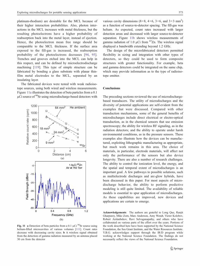
The fabricated devices were tested with weak radioiso-tope sources, using both wired and wireless measurements.Figure 11a illustrates the detection of beta particles from a 0.1µCi source of 90Sr using microdischarge-based detectors with
various cavity dimensions (8×8, 4×6, 3×6, and 3×3 mm2)as a function of source-to-detector spacing. The fill-gas washelium. As expected, count rates increased with largerdetection areas and decreased with larger source-to-detectorseparation. Figure 11b shows wireless measurements ofgamma radiation of 1.0 µCi from 65Zn. The wireless signaldisplayed a bandwidth extending beyond 1.2 GHz.
The design of the microfabricated detectors permittedflexibility in sizing and integration with other types ofdetectors, so they could be used to form compositestructures with greater functionality. For example, betaand gamma detectors could be integrated on the same chip,which may provide information as to the type of radioiso-tope emitter.
Conclusions
The preceding sections reviewed the use of microdischarge-based transducers. The utility of microdischarges and thediversity of potential applications are self-evident from theexamples that were discussed. Compared with othertransduction mechanisms, some of the general benefits ofmicrodischarges include direct electrical or electro-opticaltransduction, as in the chemical sensors that use emissionspectroscopy; the ability for wireless RF signaling, as in theradiation detectors; and the ability to operate under harshenvironmental conditions, as in the pressure sensors. Theseexamples also illustrate how the devices can be manufac-tured, exploiting lithographic manufacturing as appropriate,but much work remains in this area. The choice ofmaterials, in particular, electrode materials, will affect notonly the performance of the sensors but also devicelongevity. There are also a number of research challenges.The ability to control the ionization level, the energy, andthe spatial and temporal extent of microdischarges is animportant goal. A few pathways to possible solutions, suchas multielectrode discharges and arc-glow hybrids, havebeen discussed in this paper. For most aspects of micro-discharge behavior, the ability to perform predictivemodeling is still quite limited. The availability of reliablemodels is essential to spur application of microdischarges.As these capabilities are improved, new devices andapplications are certain to emerge.
Acknowledgements The authors are grateful to Long Que, RanjitGharpurey, Mike Zorn, Marc Anderson, Amy Wendt, Victor Kolobov,Robert Arslanbekov, Ravi Selvaganapathy, and others who havecollaborated on various parts of the effort over the years. Portions ofthe work described here have been supported by the National ScienceFoundation, the Sea Grant Institute, and the Water Resources Institute.Y.B.G. acknowledges support through the IR/D program whileworking at the National Science Foundation. The findings do notnecessarily reflect the views of the National Science Foundation.
(a)
(b)
Fig. 11 a Detection of beta particles from a 0.1 μCi 90Sr source usinghelium-filled microcavities of various volumes [111]. Count ratesdecrease with decreasing cavity sizes. b A wireless signal obtainedfrom the detection of gamma radiation measured by an antenna placed30 cm from the detector
Exploring microdischarges for portable sensing applications 573
References
1. Foest R, Schmidt M, Becker K (2006) Int J Mass Spectrom248:87–102
2. Karanassios V (2004) Spectrochim Acta Part B 59:909–9283. Miclea M, Franzke J (2007) Plasma Chem Plasma Process
27:205–2244. Broekaert J (2002) Anal Bioanal Chem 374:182–1875. Franzke J, Kunze K, Milcea M, Niemax K (2003) J Anal At
Spectrom 18:802–8076. Broekaert J, Siemens V (2004) Anal Bioanal Chem 380:185–1897. Franzke J, Miclea M (2006) Appl Spectrosc 60:80a–90a8. Braman R, Dynako A (1968) Anal Chem 40:95–1069. Lambertus G, Elstro A, Sensenig K, Potkay J, Agah M, Scheuering
S, Wise K, Dorman F, Sacks R (2004) Anal Chem 76:2629–263710. Agah M, Lambertus G, Sacks R, Wise K (2006) J Micro-
electromech Syst 15:1371–137811. Brede C, Lundanes E, Greibrokk T, Pedersen-Bjergaard S (1998)
J High Resol Chromatogr 21:633–63912. Miclea M, Okruss M, Kunze K, Ahlman N, Franzke J (2007)
Anal Bioanal Chem 388:1565–157213. Yin Y, Messier J, Hopwood J (1999) IEEE Trans Plasma Sci
27:1516–152414. Hopwood J (2000) J Microelectromech Syst 9:309–31315. MinayevaO, Hopwood J (2002) J Anal At Spectrom 17:1103–110716. Minayeva O, Hopwood J (2003) J Anal At Spectrom 18:856–86317. Engel U, Bilgic A, Haase O, Voges E, Broekaert J (2000) Plasma
Sources Sci Technol 9:1–418. Engel U, Bilgiç A, Haase O, Voges E, Broekaert J (2000) Anal
Chem 72:193–19719. Bilgiç A, Voges E, Engel U, Broekaert J (2000) J Anal At
Spectrom 15:579–55820. Schermer S, Bings N, Bilgic A, Stonies R, Voges E, Broekaert J
(2003) Spectrochim Acta Part B 58:1585–159621. Broekaert J, Siemens V (2005) IEEE Trans Plasma Sci 32:560–56122. Stonies R, Schermer S, Voges E, Broekaert J (2004) Plasma
Sources Sci Technol 13:604–61123. Iza F, Hopwood J (2003) IEEE Trans Plasma Sci 31:782–78724. Iza F, Hopwood J (2004) IEEE Trans Plasma Sci 32:498–50425. Hopwood J, Iza F (2004) J Anal At Spectrom 19:1145–115026. Hopwood J, Iza F, Coy S, Fenner B (2005) J Phys D 38:1698–170327. Liang D, Blades M (1988) Anal Chem 60:27–3128. Bass A, Chevalier C, Blades M (2001) J Anal At Spectrom
16:919–92129. Yoshiki H, Horike Y (2001) Jpn J Appl Phys 2 40:L350–L36230. Taniguchi K, Fukusawa T, Yoshiki H, Horiike Y (2003) Jpn J
Appl Phys 1 42:6584–658931. Gross R, Platzer B, Leitner E, Schalk A, Sinabell H, Zach H,
Knapi G (1992) Spectrochim Acta Part B 47:95–10632. Gibalov V, Pietsch G (2000) J Phys D 33:2618–263633. Becker K, Kogelschatz U, Schoenbach K, Barker R (2004) Non-
equilibrium air plasmas at atmospheric pressure. Institute ofPhysics, Bristol
34. Masoud N, Martus K, Becker K (2005) J Phys D 38:1674–167335. Miclea M, Kunze K, Musa G, Franzke J, Niemax K (2001)
Spectrochim Acta Part B 56:37–4336. Miclea M, Kunze K, Franzke J, Niemax K (2002) Spectrochim
Acta Part B 57:1585–159237. Kunze K, Miclea M, Musa G, Franzke J, Vadla C, Niemax K
(2002) Spectrochim Acta Part B 57:137–14638. Kunze K, Miclea M, Franzke J, Niemax K (2003) Spectrochim
Acta Part B 58:1435–144339. Zhu Z, Zhang S, Lv Y, Zhang X (2006) Anal Chem 78:865–87240. Zhu Z, Zhang S, Xue J, Zhang X (2006) Spectrochim Acta Part
B 61:916–921
41. Zhu Z, Liu J, Zhang S, Na X, Zhang X (2008) Anal Chim Acta607:136–141
42. Zhu Z, Liu J, Zhang S, Na X, Zhang X (2008) Spectrochim ActaPart B 63:431–436
43. Guchardi R, Hauser P (2003) J Anal At Spectrom 18:1056–105944. Guchardi R, Hauser P (2004) J Chromatogr A 1033:333–33845. Guchardi R, Hauser P (2004) Analyst 129:347–35146. Guchardi R, Hauser P (2004) J Anal At Spectrom 19:945–94947. Michels A, Tombrink S, Vautz W, Miclea M, Franzke J (2007)
Spectrochim Acta Part B 62:1208–121548. Stark R, Schoenbach K (1999) J Appl Phys 85:2075–208049. Frame J, Wheeler D, De Temple T, Eden J (1997) Appl Phys Lett
71:1165–116750. Schoenbach K, El-Habachi A, Moselhy M, Shi W, Stark R
(2000) Phys Plasmas 7:2186–219151. Moselhy M, Petzenhauser I, Frank K, Schoenbach K (2003) J
Phys D 36:2922–292752. Miclea M, Kunze K, Heitmann U, Florek S, Franzke J, Niemax
K (2005) J Phys D 38:1709–171553. Miclea M, Kunze K, Franzke J, Niemax K (2004) J Anal At
Spectrom 19:990–99454. Park S, Chen J, Wagner C, Ostrom N, Liu C, Eden J (2002)
IEEE J Sel Top Quantum Electron 8:139–14755. Eden J, Park S, Ostrom N, McCain S, Wagner C, Vojak B, Chen
J, Liu C, von Allmen P, Zenhausern F, Sadler D, Jensen C,Wilcox D, Ewing J (2003) J Phys D 36:2869–2977
56. Longwitz R, Van Lintel H, Renaud P (2003) J Vac Sci Technol B21:1570–1573
57. Wilson C, Gianchandani Y, Wendt A (2003) J MicroelectromechSyst 12:835–839
58. Eijkel J, Stoeri H, Manz A (1999) Anal Chem 71:2600–260659. Eijkel J, Stoeri H, Manz A (2000) J Anal At Spectrom 15:297–30060. Eijkel J, Stoeri H, Manz A (2000) Anal Chem 72:2547–255261. Bessoth F, Naji O, Eijkel J, Manz A (2002) J Anal At Spectrom
17:794–79962. Naji O, Manz A (2004) Lab Chip 4:431–43763. Mitra B, Gianchandani Y (2008) IEEE Sens J 8:1445–145464. Morris J, Krey R, Garrison R (1969) Phys Rev 180:167–18365. Mitra B, Levey B, Gianchandani Y (2008) IEEE Trans Plasma
Sci 36:1913–192466. Kushner M (2005) J Phys D 38:1633–164367. Abeysinghe D, Dasgupta S, Jackson H, Boyd J (2002) J
Micromech Microeng 12:229–23568. Fielder R, Stingson-Bagby K, Palmer M (2004) In: Proceedings
of SPIE, fiber optic sensor technology and applications III,Philadelphia, pp 60–69
69. Li T, Wang Z, Wang Q, Wei X, Xu B, Hao W, Meng F, Dong S(2007) In: Proceedings of SPIE, sensors for harsh environmentsIII, Boston, pp 1–7
70. Ned A, Okojie R, Kurtz A (1998) In: Proceedings of theinternational high temperature electronics conference, Albuquer-que, pp 257–260
71. Fricke S, Friedberg A, Ziemann T, Rose E, Muller G, TelitschkinD, Ziegenhagen S, Seidel H, Schmidt U (2006) In: Proceedingsof micro-nano-technology aerospace applications, Toulouse
72. Guo S, Eriksen H, Childress K, Fink A, Hoffman M (2008)Proceedings of the IEEE international conference on microelectro mechanical systems, Tucson, pp 892–895
73. Wright S, Gianchandani Y (2009) J Microelectromech Syst18:736–743
74. Edelmann C (1990) Vacuum 41:2006–200875. Allen D (2003) Proc Inst Mech Eng B 217:643–65076. Wright S, Gianchandani Y (2007) J Vac Sci Technol B 25:1711–
172077. Yoon J, Lee D, Nam H, Cha G, Strong T, Brown R (1999) J
Electroanal Chem 464:135–142
574 Y.B. Gianchandani et al.

78. Taylor S, Srigengan B, Gibson J, Tindall D, Syms R, Tate T,Ahmad M (2000) In: Proceedings of SPIE, chemical andbiological sensing, Orlando, pp 187–193
79. Miller R, Nazarov E, Eiceman G, King A (2001) Sens ActuatorsA. 91:301–312
80. Jenkins G, Manz A (2002) J Micromechanics Microengineering12:N19–N22
81. Cserfalvi T, Mezei P (2003) J Anal At Spectrom 18:596–60282. Kim H, Lee J, Kim M, Cserfalvi T, Mezei P (2000) Spectrochim
Acta Part B 55:823–83183. Johnson K, Wilp W, Karanassios V (2001) In: Proceedings of
SPIE, Boston, pp 347–35284. Karanassios V, Johnson K, Smith A (2007) Anal Bioanal Chem
388:1595–160485. Davis W, Marcus R (2001) J Anal At Spectrom 16:931–93786. Marcus R, Davis W (2001) Anal Chem 73:2903–291087. Wilson C, Gianchandani Y (2002) IEEE Trans Electron Devices
49:2317–232288. Que L, Wilson C, Gianchandani Y (2005) J Microelectromech
Syst 14:185–19189. Zorn M, Wilson C, Gianchandani Y, Anderson M (2004) IEEE
Sens Lett 2:179–18590. Mitra B, Wilson C, Que L, Selvaganapathy P, Gianchandani Y
(2006) Lab Chip 6:60–6591. Haugland R (1996) Handbook of fluorescence probes and
research chemicals. Molecular Probes, Eugene92. Knoll G (2000) Radiation detection and measurement. Wiley,
New York93. Hirschfelder J, Magee J, Hull M (1948) Phys Rev 73:852–86294. Shimoni U, Sheinfux B, Seidman A, Grinberg J, Avrahami Z
(1974) Nucl Instrum Methods 117:599–60395. Shafrir B, Seidman A (1975) Nucl Instrum Methods 129:177–18696. Nakamura M (1983) J Appl Phys 54:3141–314997. Kiff S, He Z, Tepper G (2005) IEEE Trans Nucl Sci 52:2932–293998. van Vuure T, van Eijk C, Fraga F, Hollander R, Margato L
(2001) IEEE Trans Nucl Sci 48:1092–109499. Veloso J, Amaro F, dos Santos J, Mir J, Derbyshire G,
Stephenson R, Rhodes N, Schooneveld E (2004) IEEE TransNucl Sci 51:2104–2109
100. Charpak G, Bouclier R, Bressani T, Favier J, Zupancic C (1968)Nucl Instrum Methods 62:262–268
101. Oed A (1988) Nucl Instrum Methods Phys Res A 263:351–359102. Francke T, Vladimir P (2003) In: Proceedings INFN ELOISA-
TRON project workshop, Erice, pp 158–179103. Charpak G, Derre J, Giomataris Y, Rebourgeard P (2002) Nucl
Instrum Methods Phys Res A 478:26–36104. Sarvestani A, Besch H, Junk M, MeiBner W, Pavel N, Sauer N,
Stiehler R, Walenta A, Menk R (1998) Nucl Instrum MethodsPhys Res A 419:444–451
105. Sauli F (2001) Nucl Instrum Meth Phys Res A 461:47–54106. Breskin A (2000) Nucl Instrum Methods Phys Res A 454:26–39107. Kyker R, Berry N, Stark D, Nachtigal N, Kershaw C (2004)
Proceedings of SPIE, digital wireless communications VI,Orlando, pp 293–304
108. Nemzek R, Dreicer J, Torney D, Warnock T (2004) IEEE TransNucl Sci 51:1693–1700
109. Brittain J (2004) Proc IEEE 92:1501–1504110. Heaton A, Reeves J (1974) In: International conference on gas
discharges, London, pp 73–77111. Eun C, Gianchandani Y (2008) J Micromechanics Microengin-
eering 18:095007112. Eun C, Gharpurey R, Gianchandani Y (2006) In: Proceedings of
the IEEE international conference micro electro mechanicalsystems, Istanbul, pp 570–573
113. Eun C, Gharpurey R, Gianchandani Y (2006) In: Proceedings ofsolid-state sensors, actuators, microsystems workshop, HiltonHead, pp 236–239
114. Petersen K (1982) Proc IEEE 70:420–457115. Belloy E, Sayah A, Gijs M (2000) Sens Actuators A 86:231–237116. West J, Jadhav A (2007) J Micromechanics Microengineering
17:403–409117. Zheng Z, Cheng W, Huang F, Yan B (2007) J Micromechanics
Microengineering 17:960–966118. Eun C, Gianchandani Y (2008) In: Proceedings of solid-state
sensors, actuators, microsystems workshop, Hilton Head, pp308–311
119. Richardson M, Gianchandani Y (2008) J MicromechanicsMicroengineering 18:015002
Exploring microdischarges for portable sensing applications 575