experiment 5. elementary gate networks
TRANSCRIPT

Experiment 5: Elementary Gate Networks by Fatih Mehmet Özçelik and Barış Bayram © 2015 All Rights Reserved. (e-mail: [email protected])
Page 1 of 11
EXPERIMENT 5. ELEMENTARY GATE NETWORKS I. Introduction
1) Objectives
In this experiment, you will get familiar with some of commonly used elementary gate
networks. In particular, multiplexer, comparator and some code converters will be
investigated and some use-cases will be studied. Throughout this experiment, logic
gate networks will be implemented by using both discrete components and Quartus II
development environment.
2) Background
2.a) Multiplexers
A multiplexer is a combinational circuit controlled by selectors, which selects and
directs one of several input lines to its output. Conventionally and ideally, a multiplexer
is a combination of m groups of n input signals per group and 𝑘 select lines, where
n=2k. However, there might be less inputs per groups than 2𝑘 . A generic block diagram
of an m-input n-bit multiplexer is given in Fig. 1.
Fig. 1: Block diagram of an m-input n-bit multiplexer

EE 314 Digital Electronics Laboratory Page 2 of 11
Based on select inputs 𝑆0 𝑆1 … 𝑆𝑘−1, output pins are controlled, e.g., if all select bits are configured as "0", output becomes 𝐼01 𝐼01 …𝐼(𝑚−1)1. As an example consider the 3-input
2x1multiplexer given in Fig. 2. In this configuration, 𝑰𝒂(𝑰𝒂𝟏𝑰𝒂𝟐), 𝑰𝒃(𝑰𝒃𝟏𝑰𝒃𝟐), 𝑰𝒄(𝑰𝒄𝟏𝑰𝒄𝟐) are the input groups, 𝒁𝟏,𝒁𝟐,𝒁𝟑 are outputs. Depending on the state of select input, 𝑺𝟏, output 𝒁𝒊, becomes equal to either 𝑰𝒊𝟏or 𝑰𝒊𝟐, where 𝒊 ∈ {𝒂,𝒃,c}. Additionally, enable pin 𝑬 is an active-low control signal, where output 𝒁𝟏 𝒁𝟐 𝒁𝟑 = 𝟎 when 𝑬=1.
Fig. 2: 3-input 2-to-1 (2x1) multiplexer
2.b) Comparators
In digital design, comparators are used for magnitude comparison, where two n-bit
numbers are inputs of the circuit. Comparators determine whether a given n-bit
number is equal to, greater or less than the second number. Conventionally, a
comparator circuit has 3 outputs corresponding to the equal, less and greater cases. As
there are 3 possible output cases, an alternative approach could be the indication of
these 3 cases by 2-bits. In Table-1, truth table of a 2-bit comparator with 2 outputs is
given. In this truth table, two 2-bit numbers, i.e., A and B, are compared by means of
their magnitude and the output is 10, 01 and 11 when A>B, A<B and A=B, respectively.

EE 314 Digital Electronics Laboratory Page 3 of 11
A B Z
A1 A0 B1 B0 Z1 Z0
0 0 0 0 1 1
0 0 0 1 0 1
0 0 1 0 0 1
0 0 1 1 0 1
0 1 0 0 1 0
0 1 0 1 1 1
0 1 1 0 0 1
0 1 1 1 0 1
1 0 0 0 1 0
1 0 0 1 1 0
1 0 1 0 1 1
1 0 1 1 0 1
1 1 0 0 1 0
1 1 0 1 1 0
1 1 1 0 1 0
1 1 1 1 1 1
Table-1: Truth table of an alternative 2-bit magnitude comparator
2.c) Code Converters
Although binary codes are widely used, in some applications other coding systems are
preferred. In rotary encoders, which track angular position changes, gray coding is in
use. The gray code has the property that a codeword in the code sequence differ by
only one bit compared to its predecessor and successor codewords. Table-2 gives the
truth table of a 4-bit binary to gray code converter.
Binary Gray
Decimal B3 B2 B1 B0 G3 G2 G1 G0
0 0 0 0 0 0 0 0 0
1 0 0 0 1 0 0 0 1
2 0 0 1 0 0 0 1 1
3 0 0 1 1 0 0 1 0
4 0 1 0 0 0 1 1 0
5 0 1 0 1 0 1 1 1
6 0 1 1 0 0 1 0 1
7 0 1 1 1 0 1 0 0
8 1 0 0 0 1 1 0 0
9 1 0 0 1 1 1 0 1
10 1 0 1 0 1 1 1 1
11 1 0 1 1 1 1 1 0
12 1 1 0 0 1 0 1 0
13 1 1 0 1 1 0 1 1
14 1 1 1 0 1 0 0 1
15 1 1 1 1 1 0 0 0
Table-2: Truth table of a 4-bit binary to gray code converter

EE 314 Digital Electronics Laboratory Page 4 of 11
II. Preliminary Work
1) Read section 4.8 - 4.11 of your course book, "Digital Design" (M. Morris Mano,
Prentice Hall) and revise manuals of experiments 1, 3 and 4 to remember FPGA
programming and hierarchical design processes.
2) Consider the logic circuit given below. It is known that this circuit is a 16-to-1
multiplexer. What should 𝐹(𝑄1,𝑄2, 𝑆3) block be?
Inputs: 𝑨𝟎𝑨𝟏…𝑨𝟏𝟓
Select Signals: 𝑺𝟑𝑺𝟐𝑺𝟏𝑺𝟎
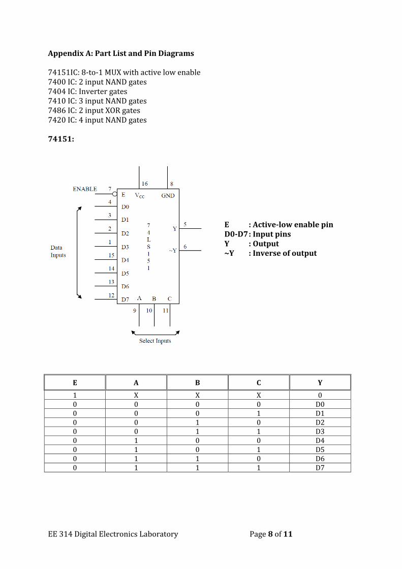
3) Design a 16-to-1 multiplexer using 74151 ICs and NAND gates. Refer to
Appendix A, for pin diagram and truth table of 74151.
4) Keeping the hierarchical design in mind, design another 16-to-1 multiplexer
using only 4-input, 3-input, 2-input NAND gates and inverters. After designing sub-
blocks on gate level, you can use block demonstrations.
5) Design a comparator circuit to compare two 4-bit numbers. As shown in Table-
1, your design should have 2 outputs, which takes the values 10, 01 and 11 for A>B,
A<B and A=B cases, respectively. This design will be implemented in Quartus II
development environment and you are not allowed to use any complex block. You
are allowed to use only NAND, NOR, XOR and INVERTER gates in your design.
6) Using the truth table given in Table-2, design a logic circuit, which converts a 4-
bit binary code to gray when select input is 1, whereas it converts gray code to
binary when the select input is 0.

EE 314 Digital Electronics Laboratory Page 5 of 11
III. Experimental Work
1) Construct the 16-bit multiplexer that you have designed in preliminary work Part-3
on the protoboard. Afterwards, test and verify that your design works as expected.
2) Draw the circuit that you have designed in preliminary work Part-4 using Quartus
II development tools. You are expected to build a hierarchical design, where final
16-to-1 multiplexer is formed by 4-to-1 multiplexer blocks. First simulate the
circuit and then implement it on FPGA board. It would be wise to use buses for
select inputs. Make sure both your simulation and implementation results are
consistent with the expectations. During development and implementation process
if you need help, you can refer to manuals of experiments 1, 3 and 4.
Important Note 1: A 16-to-1 MUX has 4 select and 16 input pins. De1-SoC board,
on the other hand, contains only 10 slide switches that we use as input elements.
Fortunately, we have also two 2x20 General Purpose Input/Output (GPIO) pins as
shown in Fig. 3. Each GPIO port contains 36 user pins directly connected to the
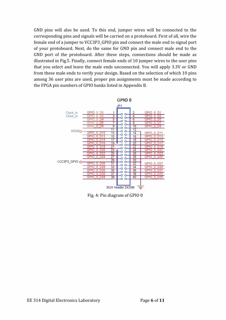
FPGA, DC 5V, DC 3.3V and two GND pins, as depicted in Fig. 4.
Fig.3 : GPIO Pins
In this part of the experiment, we will use 10 of these user pins to provide
remaining 10 inputs. As the I/O standard of the user pins is 3.3V, VCC3P3_GPIO and
EE 314 Digital Electronics Laboratory Page 6 of 11
GND pins will also be used. To this end, jumper wires will be connected to the
corresponding pins and signals will be carried on a protoboard. First of all, wire the
female end of a jumper to VCC3P3_GPIO pin and connect the male end to signal port
of your protoboard. Next, do the same for GND pin and connect male end to the
GND port of the protoboard. After these steps, connections should be made as
illustrated in Fig.5. Finally, connect female ends of 10 jumper wires to the user pins
that you select and leave the male ends unconnected. You will apply 3.3V or GND
from these male ends to verify your design. Based on the selection of which 10 pins
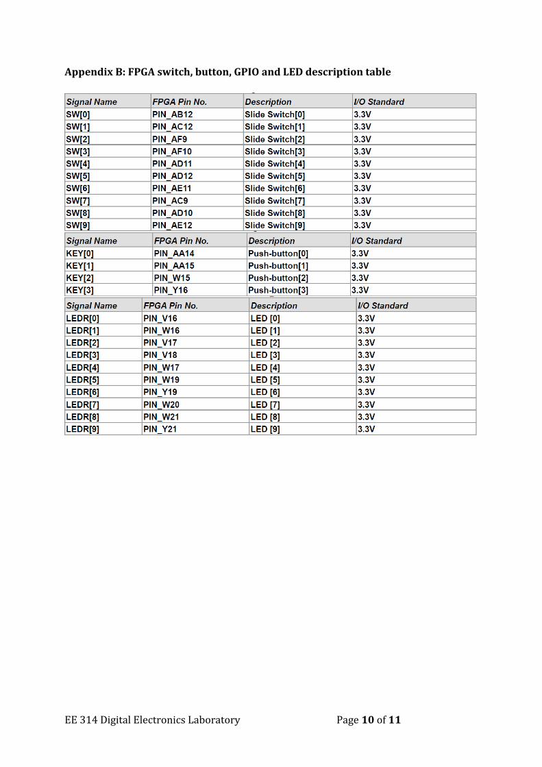
among 36 user pins are used, proper pin assignments must be made according to
the FPGA pin numbers of GPIO banks listed in Appendix B.
Fig. 4: Pin diagram of GPIO 0

EE 314 Digital Electronics Laboratory Page 7 of 11
Fig. 5: Wiring signal and gnd pins to a protobard
Important Note 2: In the previous experiment during hierarchical design steps,
you have created a new project for each low-level design block. It is also possible to
build symbol files within a single project. To do so, first create a new project and a
new schematic file. Make sure "Add file to current project" checkbox is selected.
Name the schematic same as the project name. Next, create another project file and
make sure it is also added to the current project. Draw your low-level design and
save it. Don't forget to give a proper name, i.e., a convenient name describing
functionality of the sub-block which is different than the project name. Finally,
create a new symbol from the schematic (File > Create/Update > Create Symbol
Files for Current File). Now, you can use the symbol block within the top-level
schematic file of your project, i.e. project_name.bdf.
3) Draw the comparator circuit that you have designed in preliminary work Part-5
using Quartus II schematic editor. Verify your design using simulation and then
program the FPGA and perform final tests on hardware. In this step, you are
required to use buses for inputs representing each 4-bit number.
4) Draw the binary to gray and gray to binary code converter circuits that you have
designed in preliminary work Part-6 using Quartus II schematic editor. Verify your
design using simulation and then program the FPGA and perform final tests on
hardware.
EE 314 Digital Electronics Laboratory Page 8 of 11
Appendix A: Part List and Pin Diagrams 74151IC: 8-to-1 MUX with active low enable 7400 IC: 2 input NAND gates 7404 IC: Inverter gates 7410 IC: 3 input NAND gates 7486 IC: 2 input XOR gates 7420 IC: 4 input NAND gates 74151:
E : Active-low enable pin D0-D7 : Input pins Y : Output ~Y : Inverse of output
E A B C Y
1 X X X 0 0 0 0 0 D0 0 0 0 1 D1 0 0 1 0 D2 0 0 1 1 D3 0 1 0 0 D4 0 1 0 1 D5 0 1 1 0 D6 0 1 1 1 D7

EE 314 Digital Electronics Laboratory Page 9 of 11
7400: 7486:
7404: 7420:
7410:
EE 314 Digital Electronics Laboratory Page 10 of 11
Appendix B: FPGA switch, button, GPIO and LED description table

EE 314 Digital Electronics Laboratory Page 11 of 11