experiences in pv
TRANSCRIPT

1
Department of Energy Physics:
Experiences in PV
Alexander K. Fedotov [email protected]
https://www.researchgate.net/profile/Alexander_Fedotov
https://www.researchgate.net/profile/Alexander_Mazanik
https://www.researchgate.net/profile/Mikhail_Tivanov
Belarusian State University Faculty of Physics
Department of Energy Physics
_____________________________________________________________

2
Multi-crystalline silicon
[1] Grain boundary structure and electrical activity in shaped silicon / A. Fedotov, B. Evtody, L. Fionova, Yu. Iliashuk, E. Katz, L. Poljak // Journal of Crystal Growth. – 1990. – Vol. 104. – P. 186–190; [2] Electrical activity of grain boundaries in shaped grown silicon/ A. Fedotov, B. Evtody, L. Fionova, Yu. Iliashuk, E. Katz, L. Poljak // Physica Status Solidi (A). – 1990. – Vol. 119. – P. 523-534; [3] Carrier transport in heavily doped polycrystalline silicon layers after annealing by a scanning laser beam / A.K. Fedotov, M.I. Tarasik, A.M. Yanchenko // Applied Surface Science. – 1995. – Vol. 84. – P. 379-382; [4] Transformation of electrical activity of extended defects in silicon polycrystals under annealing and hydrogen plasma treatment / A. Fedotov, N. Drozdov, E. Katz, Yu. Ilyashuk, A. Mazanik, A. Ulyashin // Physica status solidi (a). – 1999. – Vol. 171. – P. 353–363; [5] Modification of electrical activity of grain boundaries in EFG silicon under influence of hydrogen plasma / A. Fedotov, A. Mazanik, E. Katz // Interface science. – 2001. – Vol. 9. – P. 169–173; [6] Electrical activity of grain boundaries in silicon bicrystals and its modification by hydrogen plasma treatment / A. Fedotov, A. Mazanik, A. Ulyashin // Solar Energy Materials and Solar Cells. – 2002. – Vol. 72. – P. 589–595; [7] Influence of low-energy ion-beam treatment by hydrogen on electrical activity of grain boundaries in polycrystalline silicon / A. Saad, A. Mazanik, A. Fedotov, J. Partyka, P. Węgierek, P. Żukovski // Vacuum. – 2005. – Vol. 78. – P. 269-272.
0 100 200 300
1
3
5
7
3
1
No
rma
lize
d G
B c
on
ductivity
4
2
Hydrogenation time, min

3
Cu(In,Ga)(S,Se)2
[1] Photosensitivity of the structures on the Cu(In,Ga)(S,Se)2 films obtained by thermal treatment in the S and Se vapors / V.Yu. Rud’, M.S. Tivanov, Yu.V. Rud’, V.F. Gremenok, E.P. Zaretskaya, V.B. Zalesskii, T.R. Leonova, P.I. Romanov // Semiconductors. – 2007. – Vol. 41. – P. 1173 – 1177; [2] Cadmium-free thin-film Cu(In,Ga)Se2/(In2S3) heterophotoelements: fabrication and properties / V.B. Zalesskii, V.Yu. Rud’, V.F. Gremenok, Yu.V. Rud’, T.R. Leonova, A.V. Kravchenko, E.P. Zaretskaya, M.S. Tivanov // Semiconductors. – 2007. – Vol. 41. – P. 973 – 978; [3] Investigation of defects in Cu(In,Ga)(S,Se)2 films using the photocurrent decay technique / A. Saad, A. Odrinski, M. Tivanov, N. Drozdov, A. Fedotov, V. Gremenok, A. Mazanik, A. Patryn, V. Zalesski, E. Zaretskaya // Journal of Materials Science: Materials in Electronics. – 2008. – Vol. 19. – P. 371 – 374.
0,7 0,9 1,1 1,3 1,5 0,7 0,9 1,1 1,3 1,5 0,7 0,9 1,1 1,3 1,5
1
2
3
4
5
6
0
100
200
300
400
Eg, эВ Eg, эВ Eg, эВ(α
·hν)
2, (1
03·эВ·см
-1)2
1,0 мкм

4
AIIBVI semiconductors
[1] Modification of electrical properties of CdSxSe1-x films by hard irradiation and nanostructuring / A.M. Saad, A.K. Fedotov, A.V. Mazanik, M.I. Tarasik, A.M. Yanchenko, A.S. Posedko, L.Y. Survilo, Yu.V. Trofimov, N.F. Kurilovich // Thin Solid Films. – 2005. – Vol. 487. – P. 202 – 204; [2] Optical and photoelectrical properties of CdSxSe1-x films produced by screen-printing technology / M. Tivanov, E. Ostretsov, N. Drozdov, L. Survilo, A. Fedotov, Yu. Trofimov, A. Mazanik // Physica status solidi (b). – 2007. – Vol. 244, No 5. – P. 1694 – 1699; [3] Electrical, photoelectrical, and photoelectrochemical properties of electrodeposited CdTe films subjected to high-energy irradiation / A.K. Fedotov, A.A. Ronassi, Vo Thi Tuiet Vi, A.V. Mazanik, O.V. Korolik, S.M. Rabchynski, G.A. Ragoisha, E.A. Streltsov // Thin Solid Films. – 2011. – Vol. 519. – P. 7149 – 7152.
20 30 40 50 60 700
1000
2000
3000
4000
5000
6000
CdTe CdTe
Ni
Ni
Cd
Te
Ni
CdTe
Inte
nsity, arb
. units
2
CdTe
(b)

5
Nanostructured semiconductors,
composite materials for PV
[1] Photoelectrochemical and Raman characterization of In2O3 mesoporous films sensitized by CdS nanoparticles / N.V. Malashchonak, S.K. Poznyak, E.A. Streltsov, A.I. Kulak, O.V. Korolik, A.V. Mazanik // Beilstein Journal of Nanotechnology. – 2013. – Vol. 4. – P. 255 – 261; [2] Photoelectrochemical and Raman Characterization of Nanocrystalline CdS Grown on ZnO by Successive Ionic Layer Adsorption and Reaction Method / A.V. Kozitskiy, O.L. Stroyuk, S.Ya. Kuchmiy, A.V. Mazanik, S.K. Poznyak, Е.А. Streltsov, A.I. Kulak, O.V. Korolik, V.M. Dzhagan // Thin Solid Films. – 2014. – Vol. 562. – P. 56 – 62; [3] Band-gap and sub-band-gap photoelectrochemical processes at nanocrystalline CdS grown on ZnO by successive ionic layer adsorption and reaction method / M.V. Malashchonak, E.A. Streltsov, A.V. Mazanik, A.I. Kulak, S.K. Poznyak, O.L. Stroyuk, S.Ya. Kuchmiy, P.I. Gaiduk // Thin Solid Films. – 2015. – Vol. 589. – P. 145–152; [4] SnO2 / Reduced Graphene Oxide Composite Films for Electrochemical Applications / E.A. Bondarenko, A.V. Mazanik, Е.А. Streltsov, A.I. Kulak, O.V. Korolik // Materials Science and Engineering B. – 2015, DOI: 10.1016/j.mseb.2015.10.002; [6] Photocurrent switching effect on platelet-like BiOI electrodes: influence of redox system, light wavelength and thermal treatment / M.E. Kazyrevich, М.V. Malashchonak, A.V. Mazanik, E.A. Streltsov, A.I. Kulak, C. Bhattacharya // Electrochimica Acta (submitted).
Investigated objects: - Wide band-gap oxides sensitized by AIIBVI nanoparticles;
- Wide band-gap oxide / reduced graphene oxide
nanocomposites;
- BiOI layered semiconductors;

6
Carbon materials
[1] Micro Raman investigation of graphene synthesized by atmospheric pressure CVD on copper foil from decane / I.V. Komissarov, N.G. Kovalchuk, E.A. Kolesov, M.S. Tivanov, O.V. Korolik, A.V. Mazanik, Yu.P. Shaman, A.S. Basaev, V.A. Labunov, S.L. Prischepa, N.I. Kargin, R.V. Ryzhuk, S.A. Shostachenko // Physics Procedia. – 2015. – Vol. 72. – P. 450–454; [2] The significant G peak temperature shift in Raman spectra of graphene on copper / M.S. Tivanov, A.G. Praneuski, E.A. Kolesov, O.V. Korolik, A.M. Saad, I.V. Komissarov, N.G. Kovalchuk // Physica Status Solidi B (submitted); [3] Raman spectra of graphene synthesized by chemical vapor deposition on copper foil using decane as precursor / M.S. Tivanov, E.A. Kolesov, O.V. Korolik, N.G. Kovalchuk, I.V. Komissarov, V.A. Labunov // Journal of Nanoscience and Nanotechnology (submitted).
0 50 100 150 200 250 300
1604
1608
1612
1616
1620
G peak position
Linear approximation
Ram
an s
hif
t, c
m-1
Temperature, K
Slope Gcm
-1/K

7
SC modelling and parameter calculations
[1] Determination of solar cell parameters from its current-voltage and spectral characteristics / M. Tivanov, A. Patryn, N. Drozdov, A. Fedotov, A. Mazanik // Solar Energy Materials & Solar Cells. – 2005. – Vol. 87. – P. 457–465; [2] Солнечные элементы на основе полупроводниковых материалов / В.Ф. Гременок, М.С. Тиванов, В.Б. Залесский. – Минск: Издательский центр БГУ, 2007. – 222 с; [3] Effect of absorbing layer thickness on efficiency of solar cells based on Cu(In,Ga)(S,Se)2
/ M. Tivanov, L. Astashenok, A. Fedotov // Electrical Review. - 2012. - Vol. 88, № 7a. - P. 321 - 323; [4] Determination of Cu(In,Ga)(S,Se)2-solar cell parameters from quantum efficiency spectra / M. Tivanov, A. Moskalev, A. Patryn // Electrical Review. - 2015. - Vol. 91, № 9. - P. 188 – 190.

8
Calculation of solar cell parameters and operational characteristics

9
Our equipment for testing of materials and structures
Confocal spectrometer «Nanofinder-HE»
for micro-Raman and micro-PL
measurements down to 20 K
Spatial resolution 200200500 nm3
Measuring system for electric
characterization of materials and
devices in AC/DC modes at 2-300 K
and magetic fields up to 8 T
Belarusian State University Faculty of Physics
Department of Energy Physics
_____________________________________________________________

10
Belarusian State University Faculty of Physics
Department of Energy Physics
_____________________________________________________________
Development of equipment
for solar cell testing
I-V characteristics
Spectral characteristics
Lateral homogeneity (photo response
and temperature distribution)

11
Possible participation in StableNextSol COST Action
We propose to use confocal micro-Raman/Pl spectrometer for spatial-resolved investigation of solar cell photodegradation. From this point of view, laser beam can be used:
(i) as a source of optical radiation with smoothly controlled
power density, which is able to cause SC photodegradation;
(ii) for local analysis of modification in structure of the region
subjected to high energy optical impact using Raman/PL
spectra with locality 200200500 nm;
(iii) for local measurement of SC parameters (short circuit
current, open circuit voltage, etc.) before and after high energy
optical impact.

12
Alexander K. Fedotov [email protected]
Thank you for
attention
Belarusian State University Faculty of Physics
Department of Energy Physics
_____________________________________________________________
13
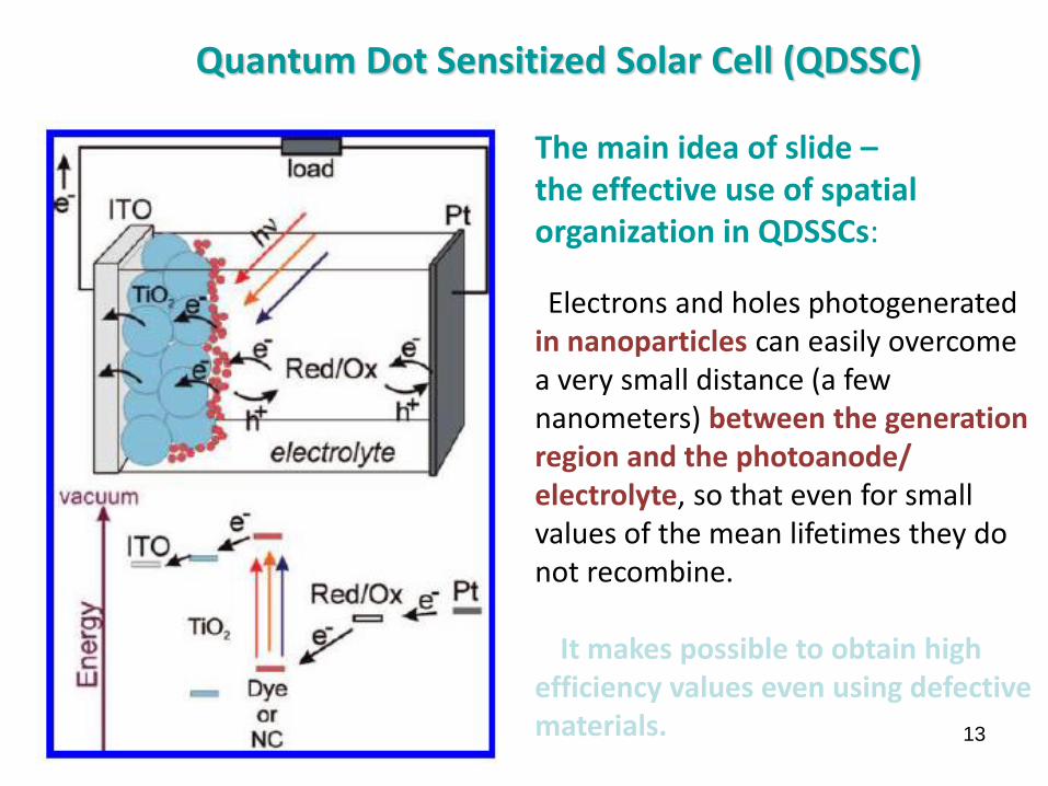
Quantum Dot Sensitized Solar Cell (QDSSC)
Electrons and holes photogenerated in nanoparticles can easily overcome a very small distance (a few nanometers) between the generation region and the photoanode/ electrolyte, so that even for small values of the mean lifetimes they do not recombine.
It makes possible to obtain high
efficiency values even using defective materials.
The main idea of slide – the effective use of spatial organization in QDSSCs:

14
Quantum Dot Sensitized Solar Cell (QDSSC)
• Possibility to control spectral range of photosensitivity varying QDs’ size;
• QDs can be synthesized using cheap wet chemistry methods;
• Spatial organization of QDSSCs allows to reach high photosensitivity using highly defective absorber materials
Main Advantages:

15
Photoanode materials: In2O3 mesoporous films (a), arrays of TiO2 nanotubes (b),
mesoporous ZnO micro-platelets (c)
The BET specific surface area is equal to 119±8 m2/g for In2O3 and 105±12 m2/g for ZnO. The specific surface area estimated from SEM results for the TiO2 nanotube array is about 10 m2/g.
(b) (a) (c)

16
The main idea of this slide - photoanode must have a high specific surface area, so it could be joined with a lot of
nanoparticles and ensure the effective absorption of light
The BET specific surface area is equal to 119±8 m2/g for In2O3 and 105±12 m2/g for ZnO. The specific surface area estimated from SEM
results for the TiO2 nanotube array is about 10 m2/g
(b) (a) (c)

17 17
Photocurrent spectra of CdS/ZnO films confirm that we really can achieve high values of the quantum
efficiency of the photoelectric conversion
Spectral dependences of External Quantum Efficiency Y presented in the coordinates Y – λ (a) and (Y∙hn)2 – hn (b) for different electrodes: ZnO (1) and
ZnO/CdS (2-6) at SILAR cycle number N = 5 (2), 10 (3), 20 (4), 60 (5) and 200 (6)
350 400 450 500 550 6000,0
0,2
0,4
0,6
0,8
1,0
Exte
rnal Q
uantu
m E
ffic
iency Y
Wavelength , nm
1
2
3 45
6
2,2 2,4 2,6 2,8 3,0 3,2 3,40
1
2
3
4
5
(Yhn)2
hn, eV
12
36
45

18
ZnO: indirect electrochemical deposition (growth of
Zn5(OH)8Cl2 with subsequent heat treatment leading
to ZnO formation);
In2O3: deposition of indium hydroxide colloidal solution
with a subsequent heat treatment ;
TiO2: anodization of metallic titanium
CdS nanoparticles: SILAR technique – sequential
immersion of substrate in Cd(NO3)2 alcohol solution,
rinsing in distilled water, immersion in Na2S aqueous
solution and the subsequent washing in distilled
water.
The cycle is repeated 5 - 300 times.
Methods of synthesis:

19
Max power:
20 mW (for 532 nm)
8 mW (for 473 nm)
2 mW (for 355 nm)
The attenuation coefficient - from 1E-6 to 1.
Belarusian State University Faculty of Physics
Department of Energy Physics
_____________________________________________________________