evaluation of optically illuminated mosfet characteristics...
TRANSCRIPT

International Journal of VLSI design & Communication Systems (VLSICS) Vol.4, No.2, April 2013
DOI : 10.5121/vlsic.2013.4202 11
EVALUATION OF OPTICALLY ILLUMINATED MOSFET
CHARACTERISTICS BY TCAD SIMULATION
Prerana Jain1 and Mishra B.K
2
1SKVM’s NMIMS,Vile Parle(W),Mumbai,India
[email protected] 2Principal, Thakur College of Engg and Technology, Mumbai
ABSTRACT
In this paper we report effect of optical illumination on Silicon MOSFET. The MOSFET has been studied in
respect of current voltage, transconductance admittance and scattering parameters. Gain analysis of the
Silicon MOSFET is done in dark and under optical illumination. The device is fabricated using ATHENA™
process simulator and the device simulation is performed using ATLAS™ from SILVACO international.
The simulation results indicate potential of MOSFET as optically sensitive structure which can be used
for increase in data transmission/reception rates, reduction of interconnect delays, elimination of clock
skew, or as a photodetector for optoelectronic applications at low and radio frequency.
KEYWORDS
AC, DC, MOSFET, Optical Illumination, RF, Simulation.
1. INTRODUCTION
Silicon CMOS technology has matured into the nanometre regime. The feasibility of RF CMOS
circuit integration has clearly been demonstrated due to reduction in gate length [1]. This
continued transistor miniaturization is the key for sustained performance improvement. But this
aggressive scaling is also associated number of higher order effects which significantly affect the
device operations. The design of RF CMOS circuits in practical systems is a real challenge due to
the strong constraints on power consumption and noise. This leaves very little margin for
design[2]. This necessitates advances in materials, device structures and other alternatives to gain
better control over the device characteristics. In spite of superior performance of compound
semiconductors, the cost issue in silicon and conventional CMOS technology devices dominates
the market place[3][4]. One of the alternatives is use of optical port to enhance the device
characteristic. Optoelectronic and CMOS integration offers all the advantages like immunity to
electromagnetic interference, better reliability etc [5]. Properties of Silicon offer possibility of
integration on the same chip. Electronic circuits, photonic circuits and micromechanical structures
can be fabricated at low cost and high reproducibility using Silicon technologies[6][7]. Silicon
detectors are also appropriate for the visible and near infrared spectral range[8]. Several
photodetector structures like photoconductors, PIN diodes and avalanche photo diodes(APD) are
available. Photoconductors and PIN diodes have no internal gain and require high are power. The
APD’s offer high gain but suffer from high amplification noise problem. Transistor photo-
detectors offer advantage of gain in comparison with diode detector structures and hence a
MOSFET under illuminated condition is considered for analysis [9].
In a device, the I-V characteristics are important at DC while Scattering (S) parameters and
admittance (Y) parameters are important at high frequency. Y and S parameters are small signal
parameters by definition and high frequency behaviour of the device is determined around a bias

International Journal of VLSI design & Communication Systems (VLSICS) Vol.4, No.2, April 2013
12
point over its operational bandwidth[10]. The S parameters are also important as they are used to
determine signal power gain and various figures of merit[11] .
Technology computer-aided design (TCAD) software is powerful tool and is widely used to
study, optimize and predict the behaviour of devices. Characterization of devices under effects of
various electrical, thermal and optical conditions is also possible [12].This paper presents analysis
of MOSFET for DC and AC under small signal condition for frequency range of 1 GHz to 10
GHz. The gain and feedback considerations are of prime importance while dealing with active
devices and hence power gain issues and their graphical displays are the starting point of analysis
and design of high frequency amplifiers. To meet this requirement the transducer gain, available
power gain, operating power gain, unilateral power gain and maximum stable power gain are
evaluated for dark and under optical radiation. Current gain analysis of the device is also
presented. Simulations are done for MOSFET under dark and optically illuminated condition. All
the calculations presented in this work have been obtained using ATLAS from SILVACO®
international unless stated otherwise. The results indicate the prospective of the device as
promising candidate for optoelectronic applications at low as well at RF frequency.
The paper is structured as follows. Section –II presents MOSFET formation in TCAD, the device
parameters, models and the methodology used for simulation under dark condition. Section III
considers MOSFET under illuminated conditions. Section IV is devoted for results and discussion
arising out of simulations.
2. THEORY
The schematic of the structure under consideration is a lightly doped drain (LDD) N channel–
MOSFET as shown in figure-1.
Figure 1. Schematic of LDD MOSFET
The conventional structure of MOSFET needs to be modified at RF to achieve the requirement of
figures of merit like low noise figure, transit frequency fT and maximum frequency of oscillation
fmax. Several modifications in the typical bulk structure have been proposed for MOSFET at RF
[4]. One of the structure is a multifinger MOSFET, which is modelled and analysed by Jain et
al.[13][14][15]. Another proposed device structures considered for present analysis is standard
LDD MOSFET.
This structure is fabricated using ATHENA which provides capability of numerical, physically-
based, two-dimensional simulation of semiconductor processing. The fabrication process in
ATHENA started with selection of wafer and completed with metallization for electrodes for a
standard LDD MOS process [16].The parameters for the device were estimated by use of
EXTRACT command. The outcome of the fabrication process simulation is the device structure
as indicated in Figure 2 and Figure 3. Figure 2 is a NMOSFET structure with materials and
junctions simulated in ATHENA. Figure 3 is the structure with net doping profile of the
NMOSFET.

International Journal of VLSI design & Communication Systems (VLSICS) Vol.4, No.2, April 2013
13
Figure 2. MOSFET structure with materials and junctions in TCAD
Figure 3.MOSFET structure with net doping profile.
The NMOSFET simulated uses a p type substrate of concentration of 1 x 10¹⁷ atoms/cm3 with an
ion implanted profile. The surface concentration under the channel is 3.74188 x 10¹⁶ atoms/cm3.
The gate oxide is 10nm thick deposited by dry oxidation process. The fabricated junction depth
achieved is about 0.17µm. The source and drain structures have been processed to achieve LDD
structure. The drain and source regions have peak concentration of 5.36 x 10²⁰ atoms/cm3 and the
lightly doped region has concentration of 2 x 10¹⁷
atoms /cm3. The gate is made of n doped
polysilicon while the source and drain electrodes are of Aluminium. The gate length of the device
is 0.36µm. The long channel threshold voltage of the fabricated structure extracted is 0.6V. The

International Journal of VLSI design & Communication Systems (VLSICS) Vol.4, No.2, April 2013
14
device fabrication is done using two dimensional simulator, and hence the device width is 1µm
unless specified. Atlas is two and three dimensional physically based device simulator. Simulation in ATLAS
requires appropriate mesh definition. It has been demonstrated that inappropriate mesh spacing
often affects accuracy of simulation. The mesh structure of MOSFET is presented in figure 3.
Lateral spacing in the channel under the gate and source drain region is small. Similarly very
small vertical mesh spacing is selected in the channel under the gate for optimized simulation
considering speed and accuracy of simulation.
Figure 4. Mesh structure of MOSFET
The numerical simulation of MOSFET is carried out using MOS models in the ATLAS. MOS
parameter enables Shockley-Read-Hall (SRH), Fermi Statistics (FERMI), and the Lombardi
Mobility model (CVT) for transverse field dependence. The CVT model sets a general purpose
mobility model to include concentration, temperature, parallel field and transverse field effects.
The SRH model accounts for recombination effects, and uses fixed minority carrier lifetimes.
The contact statement is used to define gate electrode which is n doped poly silicon for which the
simulator assumes work function of 4.7 eV.For accurate simulation of MOS devices the interface
charge at the oxide, must be considered. This is done by setting the QF parameters for the
INTERFACE statement to a value of 3x10¹⁰ /cm2 [17]
Several numerical methods are available and can be used for calculating the solutions to
semiconductor device[18]. In the ATLAS tool a method or combination of methods is selected
depending on the equations to be solved. For the MOS structure the trend is to simulate only
majority carriers to improve speed of simulation. But this is not advised when the simulation
involves small signal ac analysis or when recombination effects are to be considered. To calculate
electrical parameters, the simulator makes use drift diffusion formulation discretized over a multi-
dimensional numerical mesh[19]. The isothermal drift diffusion model requires the solution of
three decoupled equations for potential, electron concentration, and hole concentration.

International Journal of VLSI design & Communication Systems (VLSICS) Vol.4, No.2, April 2013
15
This solution was achieved by use of Gummel Newton iteration scheme. This method initially
performs a GUMMEL iteration to obtain an improved initial guess for the NEWTON solution
scheme. This is slow but reliable way of obtaining solutions for any device[20]. For device
analysis under any applied bias, first initial solution must be performed with zero bias for initial
guess to determine potential and carrier concentrations from the doping profile. The simulator
solves the three basic equations using drift diffusion model evaluating for potential, electron
concentration and hole concentration with appropriate assumptions and calculates the drain
current[21]. The drain current under dark condition was evaluated by ramping the bias in small initial steps.
The ATLAS tool calculates the drain current under varying gate bias and drain bias, but the
transconductances cannot be obtained directly. TONYPLOT™ is used which is a graphical post
processing tool for use with all SILVACO simulators. The transconductances are obtained
graphically using TONYPLOT functions from the plot of drain current with respect to gate and
drain voltages by taking derivatives as per (1). The gate transconductance gm and the drain
conductance gds are given by
(1A)
(1B)
The ac analysis is performed to determine small signal characteristics of the device. Instead of
extracting a small-signal model from measurements, the complete small-signal model of the
intrinsic device is derived from physically-based simulations. Several advantages can be achieved
by use of this methodology. Errors resulting from measurements and extraction of extrinsic
component are decoupled; Non Quasi Static (NQS) effects are included by default resulting in a
good description of the electrical performance, even at frequencies beyond transition frequency
fT. Parameter extraction between any two ports of the device is easily feasible which is difficult
otherwise [22].
The ATLAS tool supports calculation of various AC parameters like Hybrid (H), Admittance(Y),
Impedance (Z), Scattering(S) etc. The gain analysis can also be done as a part of small signal
analysis. AC sinusoidal small-signal analysis should be performed after solving for a DC
condition. The full Newton method must be used for this analysis. Frequency range of interest,
device width and the method for ac analysis has to be selected. A direct parameter is included
which is robust for all range of frequencies. The gate terminal is selected as input port where ac
bias will be applied, while drain terminal is selected as output port indicating that device works in
common source configuration.
Design of high frequency circuits is often done with help of Y parameters. The device simulator
does not make a distinction between the intrinsic and parasitic parts of the device. The Y
parameters are simulated using the (2) for each DC bias condition as in[11].
jkjkjk cjgy ω+=− (2)
The yjk parameters are obtained by applying a small-signal voltage at the kth terminal and detecting
current at the jth terminal while all other terminals are AC grounded with following relationship
constVVV
Igg DS
GB
DSmmg =
∂
∂== ,
constVVV
Igg DG
DB
DSdsmd =
∂
∂== ,

International Journal of VLSI design & Communication Systems (VLSICS) Vol.4, No.2, April 2013
16
k
j
jkv
iy = (3)
Admittance or impedance parameters require short circuit or open circuit condition for
measurement, which is difficult to achieve at high frequency where lead inductance and parasitic
capacitances dominate the measurement. [13].Scattering or S parameters are alternative to
admittance or impedance parameters for characterization at high frequency. S parameters are
relatively simple to measure, conceptually simple, analytically convenient and capable of
providing a great insight into measurement or design problem. The S parameters can be obtained
from Y parameters using Y to S conversion for the desired characteristics impedance as in[23,24].
The expressions for gain and unilateral figure of merit are obtained from S parameters and
reflection coefficients. The source(ГS), load(ГL), input(Гin) and output(Гout) reflection coefficients
have same definitions as in [23].
The transducer power gain GT, quantifies the gain of the amplifier placed between source and
load.
(4A)
An often employed approximation for the transducer power gain is the so-called unilateral power
gain, GTU, which neglects the feedback effect of the amplifier (S12 = 0). It is often used as a basis
to develop approximate designs for an amplifier and its input and output matching networks.
(4B) The available power gain GA for load side matching (TL, = Tout) is defined as
(4C)
The operating power gain is the ratio of the power delivered to the load to the power supplied to
the amplifier.
(4E)
The current gain h21 of a small-signal common-source amplifier stage is defined as
11
212
1
1 21
Y
Y 0
I
I=== Vh
(4F) The calculation of current gain h21 is important as it can be used to evaluate frequency ft .
Transition frequency ft also known as unity gain frequency and is one of the figure of merit for
RF operation and indicates the frequency at which current gain h21 equals one.
3. MOSFET UNDER ILLUMINATION
When light falls on the surface of a semiconductor material, photons whose energy is in greater
than that of the band-gap energy of the semiconductor material, are absorbed. This absorption
excites an electron to jump into the conduction band and as a result a hole is left in the valence
band. These promoted electrons and valence band holes behave as free particles and travel under
intrinsic or externally-applied electric field. This continuous separation of electron-hole pairs due
212212211
2221
2
)1)(1(
)1()1(
SLLS
SL
T
SSSS
S G
ΓΓ−Γ−Γ−
Γ−Γ−=
211
222
2221
2
11
)1()1(
SL
SL
TU
SS
SG
Γ−Γ−
Γ−Γ−=
211
2
2221
11(
)1(
Sout
S
A
S
SG
Γ−Γ−
Γ−=

International Journal of VLSI design & Communication Systems (VLSICS) Vol.4, No.2, April 2013
17
to the absorption of photons enhances the conductivity. This photocurrent is directly proportional
to the intensity of the incident light.
The schematic of MOSFET under illumination is as shown in figure 5. The Aluminium electrodes
block the incident light, but the light can be absorbed at the edge of the gate electrodes. This
modifies the depletion region width of the drain(YdD) and source(YdS) region and hence the
depletion region width at gate(YdG). Silicon is sensitive to UV, visible and near-infrared regions
i.e. from around 200 nm to 1100 nm of wavelength. The peak response can be modified to suit
specific applications using special antireflection coatings and filters [9]In the present work no
such modification has been done.
Figure 5. Schematic of MOSFET under illumination.
The ATLAS framework includes LUMINOUS which is optoelectronic simulator. LUMINOUS is
a general purpose ray trace and light absorption program which calculates optical intensity
profiles within the semiconductor device, and converts these profiles into photo generation rates.
This unique coupling of tools allows simulation of electronic responses to optical signals for a
broad range of optical detectors. For the simulation purpose an optical source originates 0.5um
above the device, perpendicular to the front surface of the device is considered. The wavelength
of the source is 830nm with intensity of 0.25 mW/cm2 assumed to be incident over the MOSFET.
Presently, it has been found extensively that lot of systems for home–networking and chip–to–
chip interconnect make use of wavelength less than 850nm and hence is chosen for
simulation.[8]
The SRH, CONMOB, AUGER and FLDMOB models activated for simulation. The effect of the
transmission coefficients, reflection coefficients, along with the integrated loss due to absorption
over the ray path is considered for each ray. This computation due to the cumulative effect is
saved for each ray. The generation associated with each grid point can be calculated by
integration of the generation rate formula as in equation (5). The calculation for the generation
rate is then performed over the area of intersection between the ray and the polygon associated
with the grid point.
yehc
PG αα
λη −=
*
0 (5)
Where
P* contains the combined effects of loss due to absorption, reflections and transmissions.
ηo represents number of carrier pairs generated per photon and is measure of internal quantum
efficiency
y is a relative distance for the ray.
h is Planck’s constant
International Journal of VLSI design & Communication Systems (VLSICS) Vol.4, No.2, April 2013
18
λ is the wavelength.
c is the speed of light.
α is the absorption coefficient.
The simulator calculates source photo current IS and available photocurrent IA. The source photo
current can be considered as a measure of the rate of photons incident on the device expressed as
a current density and is given by(6).
tn
s Whc
BqI
λ= (6)
The available photocurrent can be thought of as a measure of the rate of photo absorption in the
device expressed as a current density. This is less than the source photocurrent. The losses are due
to reflection and transmission of light out of the device structure.
∑ ∫=
−=R
i
iN
i
y
x
iiRn
A dyePWhc
BqI
1 01
ααλ
(7)
Where
Bn is the intensity in beam number n,
λ is the source wavelength,
h is Planck's constant,
c is the speed of light,
Wt is the width of the beam including the effects of clipping,
NR is the sum is taken over the number of rays traced,
WR is the width associated with the ray,
Yi, is the integral is taken over the length, associated with the ray,
Pi accounts for the attenuation
αi is the absorption coefficient in the material that the ray is traversing,
To account for the diffraction or coherent effects beam propagation method is used.The total
current under illumination is the addition of dark current and the current due the carriers
generated due to photons.
4. RESULTS AND DISCUSSION
The device under consideration is a Silicon N-MOSFET with a LDD structure. The gate length is
0.36 µm and the width is 1µm for DC analysis. The drain current is calculated by varying gate
and drain voltage in small steps, one at a time, since the equations are solved by numerical
methods. The simulation has been performed for the device in dark condition and also under
optical illumination for incident wavelength of 830nm and beam intensity of 0.25 mW/cm2.
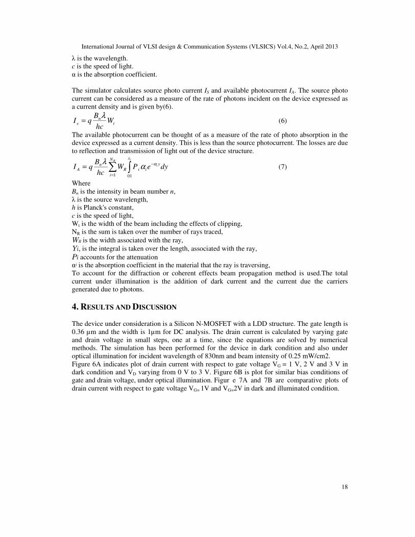
Figure 6A indicates plot of drain current with respect to gate voltage VG = 1 V, 2 V and 3 V in
dark condition and VD varying from 0 V to 3 V. Figure 6B is plot for similar bias conditions of
gate and drain voltage, under optical illumination. Figur e 7A and 7B are comparative plots of
drain current with respect to gate voltage VG= 1V and VG=2V in dark and illuminated condition.
International Journal of VLSI design & Communication Systems (VLSICS) Vol.4, No.2, April 2013
19
Figure 6 Figure 6.2
Figure 6A:Drain current Vs Drain voltage for VG=1V, 2V and 3V in dark condition
Figure 6B: Drain current Vs Drain voltage for VG=1V, 2V and 3V under optical illumination.
Figure 7(A) Figure 7(B)
Figure 7A: Drain current Vs Drain voltage for VG= 1V in dark & under optical illumination.
Figure 7B: Drain current Vs Drain voltage for VG= 2V in dark & under optical illumination.
It can be seen that there is appreciable increase in drain current under optical illumination for
varying gate voltage VG as compared to dark condition. This is because incident radiation results
in excess electron hole pair generation in the depletion region. Because of this, photo
voltage(VOP) is developed modifying the effective gate bias to VG+VOP. This higher effective
gate bias enhances the device conductivity and hence the drain current increases.
Figure 8A and Figure 8B are plots of drain current with respect to varying gate voltage VG from 0
V to 3 V with VD=0.1 V and 1 V in dark and under optical radiation. Again here similar effect is
observed that drain current increases under light. Conventionally drain current-gate voltage
characteristics are used to evaluate threshold voltage. It can be seen that the effective threshold
voltage reduces under influence of optical radiation confirming that photovoltage develops across
the gate. The effect of optical radiation is more pronounced with increasing drain bias from 0.1 V
to 1 V for constant gate voltage because the depletion width of the MOSFET is affected by drain
bias.

International Journal of VLSI design & Communication Systems (VLSICS) Vol.4, No.2, April 2013
20
Figure 8(A) Figure 8(B)
Figure 8A: Drain current Vs Gate voltage for VD= 0.1 V in dark & under optical illumination.
Figure 8B: Drain current Vs Gate voltage for VD= 1 V in dark & under optical illumination
Figure 9(A) Figure 9(B)
Figure 9A. Drain Conductance Vs Drain voltage for VG=1V in dark & under illumination.
Figure 9B. Drain Conductance Vs Drain voltage for VG= 2V in dark & under illumination.
Figure 9A and Figure 9B are plots of drain conductance under varying voltage with VG of 1 V
and 2 V.The graphs signify that drain conductance is almost constant with increasing drain
voltage. The output conductance is proportional to the drain current, and since drain current is
almost constant in saturation region of MOSFET at higher drain voltage, output conductance also
becomes independent with increasing drain bias. It can be seen that drain conductance remains
constant in dark as well as with photon flux radiation. Thus this verifies that optical flux modifies
the effective gate bias than drain bias.
Figure 10A and Figure 10B are plots of gate transconductances at fixed drain voltage of 0.1 V
and 1 V with varying gate voltage. The drain current is very small till the device enters inversion
as indicated in Figure 8 Due to this the change in device gate transconductances is seen at higher
gate voltage as seen in Figure 10. The transconductances curve reaches a peak and then remains
almost constant. This is due to influence of VGS on effective mobility. The nature of plots of
transconductance are not similar for VD= 0.1V and 1V. This is because the device is in linear
region for VD=0.1V and is in saturation for VD=1V. The transconductance is one of the very
important factors considered in circuit design as it decides transit frequency. Thus the optically
modulated device can be used to as an additional control for the device operation.
International Journal of VLSI design & Communication Systems (VLSICS) Vol.4, No.2, April 2013
21
Figure 10(A) Figure 10(B)
Figure 10A: Transconductance Vs Gate voltage for VD=0.1V in dark & under illumination.
Figure 10B: Transconductance Vs Gate voltage for VD= 1V in dark & under illumination.
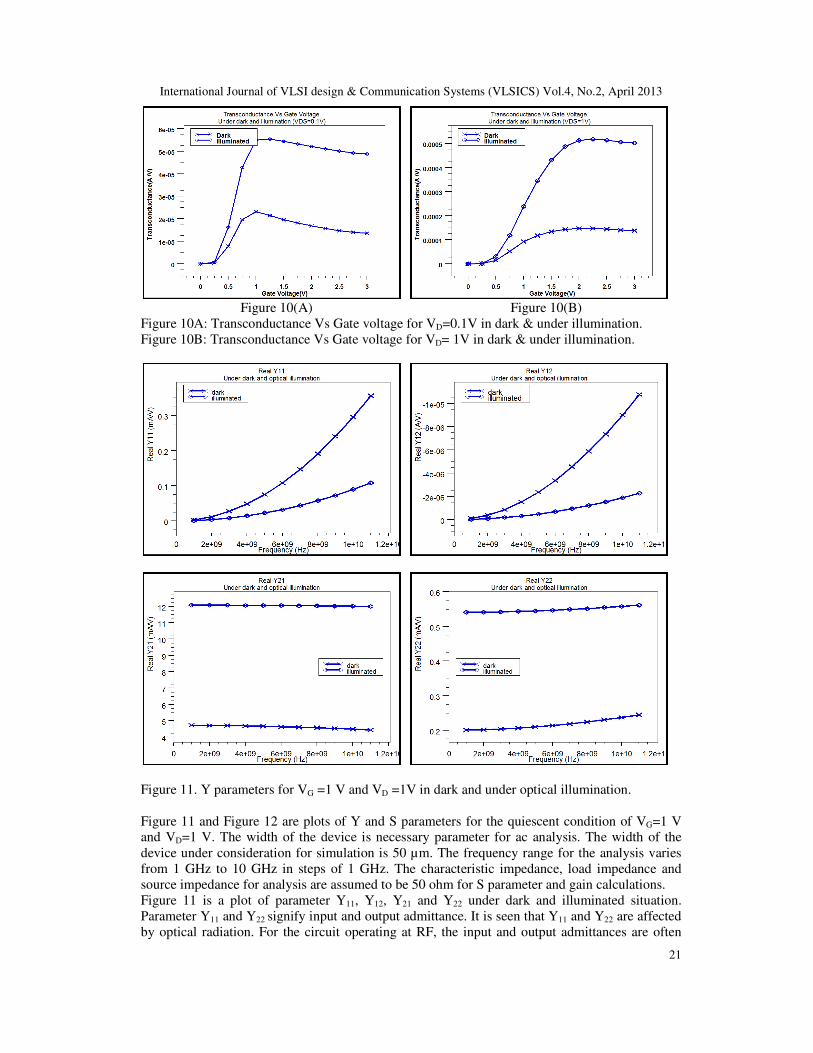
Figure 11. Y parameters for VG =1 V and VD =1V in dark and under optical illumination.
Figure 11 and Figure 12 are plots of Y and S parameters for the quiescent condition of VG=1 V
and VD=1 V. The width of the device is necessary parameter for ac analysis. The width of the
device under consideration for simulation is 50 µm. The frequency range for the analysis varies
from 1 GHz to 10 GHz in steps of 1 GHz. The characteristic impedance, load impedance and
source impedance for analysis are assumed to be 50 ohm for S parameter and gain calculations. Figure 11 is a plot of parameter Y11, Y12, Y21 and Y22 under dark and illuminated situation.
Parameter Y11 and Y22 signify input and output admittance. It is seen that Y11 and Y22 are affected
by optical radiation. For the circuit operating at RF, the input and output admittances are often

International Journal of VLSI design & Communication Systems (VLSICS) Vol.4, No.2, April 2013
22
terminated at characteristics admittance by use of matching network, hence the effect on
impedance can be treated as insignificant. The parameter Y21 signifies device forward gain or
transconductance which is one of the most important parameter. The comparative plot of
parameter Y21 in dark and illuminated condition signifies that illumination enhances the
transconductance of the device, making it more suitable for RF operation. On other hand the plot
for parameter Y12 indicates that reverse gain decreases.
Figure 12: S parameters for VG and VD of 1V in dark and under optical illumination
Figure 12 is a plot of parameter S11, S12, S21 and S22 under dark and illuminated situation. S and Y
parameters for the device are inter-convertible and hence similar effect is observed for S
parameters. The S11 and S22 are related with input and output impedances and reflect similar effect
as that of Y11 and Y22. Parameter S21 which is associated with forward gain of the device increases
with light impeachment. It can be seen that device transconductance in DC or AC always
improves with optical radiation and this is reflected in parameter S21.
Figure 13 are plots of available power gain, maximum stable power gain, maximum transducer
power gain and unilateral power gain for frequency of 1 GHz to 10 GHz in dark and under optical
illumination. The plots show that there is increase in gain under optical illumination for the
frequency range under consideration. The rise of gain is consistent even with rise in frequency.
The rise in gain is seen as the forward gain S21 of the device increases, while reverse gain is
almost unaffected by optical illumination, contributing to enhancement of power gain for the
device under illuminated condition.

International Journal of VLSI design & Communication Systems (VLSICS) Vol.4, No.2, April 2013
23
Figure 13: Power gain for VG and VD of 1V in dark and under optical illumination
Figure 14A Figure 14B
Figure 14A and 14B: Current gain for VG and VD of 1V in dark and under illumination
Figure 14A is plot of current gain for frequency of 1 GHz to 10 GHz in dark and under optical
illumination. The optically illuminated MOSFET shows advancement in the current gain of the
device, thus indicating improvement in the transition frequency of the device. Figure 14B is the
plot of current gain for frequency of 1 GHz to 40 GHz in dark and under optical illumination, to
locate transition frequency ft. The transition frequency is the frequency at which current gain is
equal to one in magnitude or 0 dB. Using interpolation technique and extract command, the
transition frequency in dark condition is found to be 13.65GHz and under optical radiation is
36.480 GHz. The substantial rise in transition frequency can be contributed to increase in drain
current and hence improvement in transconductance. Thus significant improvement seen in

International Journal of VLSI design & Communication Systems (VLSICS) Vol.4, No.2, April 2013
24
transition frequency proves that optical radiation of the NMOSFET aids in rise of figure of merit
at RF.
5. CONCLUSIONS
The optical response of lightly doped drain N-channel Silicon MOSFET has been studied using
SILVACO TCAD software. The simulation been carried out using appropriate models and
suitable numerical methods for dark condition and under optical radiation. The effect of optical
illumination has been studied for dc and ac characteristics. The increase of drain current,
conductances and transconductances of the optically illuminated device is contributed to
modulation of channel conductivity due to incident photon flux.
RF performance of the device for frequency range of 1 GHz to 10 GHz is also investigated. The
variations of admittance and scattering parameters indicate that the device capacitances are
sensitive to light. This can property can be used to design optical mixers and oscillators. The
improvement in transconductance and the forward current gain signify that device can be used as
an optically controlled amplifier with low noise at RF. The effect on power gain and the transit
frequency of the device has also been studied. The simulation results indicate prominent
improvement in transit frequency and the boost in power gain of the device.
The increase in drain current, enhancement of ac and dc transconductances and the boost of
power gain at RF suggest that the device is a promising candidate for optoelectronic applications
at DC and RF. The present device structure is suitable for wavelength upto 1100 nm.
Modification of device structure is likely to extend the range of incident wavelength to 1500 nm
making it suitable for long haul communication.
ACKNOWLEDGEMENTS
The authors would like to thank Department of Electronics, North Maharashtra University,
Jalgaon, for providing usage of TCAD software by SILVACO international.
REFERENCES
[1] M.Jamal deen and Tor A. Fjeldly, "Preface," in CMOS RF Modelling,Characteruzation and
Applications,Selected Topics in Electronic Systems, M.Jamal deen and Tor A. Fjeldly, Eds.
Singapore: World Scientific Publishing Co.Pte Ltd, 2001, vol. 24, ch. Preface.
[2] Y. Cheng, "MOSFET Modelling for RF IC Design," International Journal of High Speed Electronics
and Systems, vol. 11, no. 4, pp. 1007-1084, 2001.
[3] H.Zimmerman, Silicon Photodetectors and Receivers, H.Zimmerman, Ed.: Springer, 2000.
[4] Juin J. Liou and Frank Schwierz, "RF MOSFET: Recent Advances, Current status, and Future
trends," Solid-State Electronics, vol. 47, pp. 1881–1895, May (2003).
[5] Jasprit Singh, Semiconductor Optoelectronics.: McGraw-Hill Inc, 1995.
[6] Dana Cristea, "Silicon Opto-FET for Photonic Integrated Circuits," in EDMO 2001, Vienna, 2001,
pp. 273-279.
[7] J.D. SCHAUB et al., "Lateral PIN photodiodes for high-speed silicon optical receivers," IEEE,
Industrial Research Highlights 2002.
[8] Chu-Hsuan Lin and Chee Wee Liu, "Review Metal-Insulator-Semiconductor Photodetectors,"
Sensors, vol. 10, pp. 8797-8826;, September 2010.
[9] Abid Kamran, "Gated Lateral Silicn P-I-N junction photodiodes," University of Glasgow, PhD thesis
2011.
[10] Jaejune Janguse, "Small Signal Modelling of RF CMOS," Stanford University, PhD Thesis 2004.
[11] Prerana Jain, Mishra B.K., and Gayatri Phade, "Power Gain Analysis of Optically Illuminated
MOSFET," International Journal Of Computer Applications, vol. 51, no. 16, pp. 50-54, August 2012.
International Journal of VLSI design & Communication Systems (VLSICS) Vol.4, No.2, April 2013
25
[12] G.A.Amstrong and C.K.Maiti, TCAD Design for Si,SiGe and GaAs Integrated Circuits. London,
U.K.: IET, 2007.
[13] Jain Prerana and Mishra B.K., "An Invesigation of DC characteristics in Multifinger Optically
Illuminated MOSFET," International Jornal of Computer Applications, vol. 61, no. 2, pp. 12-17,
January 2013.
[14] Jain Prerana and Mishra B.K., "CV Investigation in Optically Illuminated MOSFET," International
Journal of Engineering Research and Applications, vol. 47, pp. 1881-1885, Nov-Dec 2012.
[15] Prerana Jain, Mishra B.K., and Phade Gayatri, "AC performance of Optically Controlled MOSFET,"
in SCEECS, Bhopal, 2012.
[16] "Athena USER manual," 2010.
[17] "ATLAS User Manual," 2010.
[18] Christopher M. Snowden, Semiconductor Device Modelling, 1st ed. Oxford, Great Britain: Springer
Veralag, 1989.
[19] Bert Kerr, Carl L. Axness, Jason C. Verley, Charles E. Hembree, and Eric R. Keiter, "A new time-
dependent analytic model for radiation induced photocurrent in finite 1D epitaxial diodes," Sandia
National Labrotaries, 2012.
[20] X. Li, W. Wu, H. Wang, A. Jha, R. van Langevelde, G.D.J. Smit, A.J. Scholten G. Gildenblat, "PSP:
An Advanced Surface-Potential-Based MOSFET Model for Circuit Simulation," IEEE Trans.
Electron Dev, vol. 53, no. 9, pp. 1979–1993, 2006.
[21] D. Vasileska, D. Mamaluy, H. R. Khan, K. Raleva, and S. M. Goodnick, "Semiconductor Device
Modeling," Journal of Computational and Theoretical Nanoscience, vol. 5, pp. 1-32, 2008.
[22] Jörgen Olsson, "SILICON RF-DEVICES," Top Amplifier Research Groups in a European Team,
Sweden, Tutorial 2004.
[23] Reinhold Ludwig, RF Circuit Design,Theory and Applications. New Jersey: Prentice Hall, 2000.
[24] Prerana Jain, B.K. Mishra, and Phade G., "S parameters of Optically Illuminated MOSFET," in
International Conference on Advancements in Engineering and Management(ICAEM), Hyderabad,
2012.
Authors
Dr.B.K.Mishra was born in 5th
June 1966,in Bihar He completed his B.E. in Electronics
Engg in 1988 and M.E. in Electronics and Communication Engg in 1992. He was
awarded PhD degree from Birla Institute of Technology in 1998. He has 23years of
teaching experience. His present research interest focuses on device and structures
working at microwave frequencies and optical sensors. He is presently working as
Principal at Thakur College of Engineering and Technology, Kandiwali, Mumbai..
Prerana Jain born on 30th Nov 1969, completed her graduation in Electronics and
Telecommunication in 1991 from Pune University. She completed her Mtech in VLSI
Technology from North Maharashtra University in 2007 and has work experience of 20
years in industry and teaching. Presently she is pursuing PhD under guidance of
Dr.B.K.Mishra. Her research area is semiconductor device modelliing for optoelectronic
applications. She is presently working as Asst Prof in North Maharashtra university,
Jalgaon.