evaluation of iec 61175 for semantic interpretation in ...789016/fulltext01.pdf · degree project...
TRANSCRIPT

Degree project in
Evaluation of IEC 61175 for semanticinterpretation in OPAL-RT referencedistribution network and Jess-OPC
CLIPTON CHOWDHURY
Stockholm, Sweden 2014
XR-EE-ICS 2015:002
ICSMaster thesis

Evaluation of IEC 61175 for semantic interpretation inOPAL-RT reference distribution network and Jess-OPC
environment
byc© Clipton Chowdhury
A thesis submitted to theSchool of Electrical Engineering
in partial fulfilment of therequirements for the degree of
Master of Science in Electric Power Engineering
Department of Industrial and Control SystemKTH
15 October 2014

Abstract
In the past few decades the electric power system has seen tremendous growth in termstechnology such as integration of DG and advanced power electronics devices. Such devel-opments mainly include renewable energy, increased use of HVDC transmission, state ofthe art communication systems and adaptation of information modeling standards appliedto power systems. In this thesis work a RBTS distribution grid network model has beenimplemented in OPAL-RT to integrate automation and ICT with more devices. These mo-tivate use of standardization like IEC 61850 and IEC 61175. This network model is usedfor verification of earlier developed monitoring and control methods at the ICS department.The verification setup involves interfacing of the network models in OPAL-RT with Jessrule engine via OPC. The focus of this master project work is evaluation of the use of IEC61175 for consistent signal naming in the network model. It is done through detailed signalmodeling in the Simulink model for use in the real time simulation and implementation ofa graphical user interface to show all the signals along with their measured value in a treeview. Second part of the work focuses on utilization of the signal modeling in high-levelapplications. The applications can utilize the consistent signal naming done by using IEC61175 to implement a semantic reasoning model for interpretation of the signals and therebyimprove the monitoring and control functions. An interface has been implemented to gen-erate an XML file of the mapped signals along with the last measured value for the parserimplemented in Java. After parsing the XML file all the data is used for the Jess rule engineto fire the particular rule in a specific situation. Some rules are implemented for monitoringthe system voltage and for finding out the signals associated with distributed generationunit to calculate their actual generation in the network. In this project an ontology basedapproach is also performed in JADE to get a clear idea of integration of information sources.Results of the work show that proper signal designation in a network according the standardIEC 61175 can potentially help reduce the complexity and improve reliability of operations.
ii

Abstrakt
Under de senaste decennierna ökade elkraftsystemet ökade enormt i tekniska termersom integration av DG och avancerade ström i elektroniska enheter. En sådan utveck-ling innefattar främst förnybar energi, ökad användning av HVDC-överföring, toppmodernakommunikationssystem och anpassning av informationsmodelleringskraven för kraftsystem.I detta examensarbete har ett RBTS distributionsnätet nätverksmodell genomförts i OPAL-RT för att integrera automation och IT med fler enheter. Dessa motiverar användningenav standardiseringen som IEC 61850 och IEC 61175. Denna nätverksmodell används förverifiering av tidigare utvecklade processer och kontrollmetoder vid ICS avdelningen. In-stallationsveriferingen innebär gränssnitt för nätverksmodeller i OPAL-RT med "Jess ruleengine" via OPC. Fokus i detta examensarbete är utvärdering av användningen av IEC 61175för en konsekvent namngivning av signalen i nätverksmodellen. Det görs genom noggrannsignalmodellering i Simulink-modellen för användning i realtidssimulering och genomförandeav ett grafiskt användargränssnitt för att visa alla signaler tillsammans med mätvärdet i enträdvy. Andra delen del av arbetet har varit fokuserar Utnyttjande av signal modelleringi hög nivå applikationer att fokusera utnyttjandet av signalmodelleringen görs med hjälpav IEC 61175 att genomföra en semantisk resonemang modell för tolkning av signalernaoch därmed förbättra övervakningen och kontrollfunktioner. Ett gränssnitt har genomförtsför att skapa en XML-fil av de kartlagda signalerna tillsammans med det senast uppmättavärdet för tolken genomfört i Java. Efter tolka XML-filen alla data används för "Jess ruleengine" att avfyra särskild regel i en specifik situation. Vissa regler tillämpas för övervakn-ing av systemspänning och för att ta reda på de signaler som förknippas med distribueradgenereings enheter för att beräkna deras faktiska produktion i nätet. Projekt är ontologinbaserad på metoder upprätt i JADE för att få en klar uppfattning om ntegreringen av infor-mationskällorna. Resultatet av arbetet visar att korrekt beteckning av signalen i ett nätverkenligt standarden IEC 61175 kan hjälpa potentiellt förenkla och förbättra tillförlitligheten iverksamheten.
iii

Acknowledgements
First and foremost, I would like to express my sincere gratitude to my supervisors Dr. Ar-shad Saleem, PostDoc research fellow at the Department of Industrial Information and Com-munication System (ICS) ,Royal Institute of Technology(KTH) and Nicholas Honeth,PHDstudent at ICS,The Royal Institute of Technology(KTH), who have supported me through-out my thesis with their patience and knowledge. Their guidance helped me in all the timeof research and writing of this thesis.I could not have imagined having better supervisorsand mentors for my Master thesis.
Beside my supervisors, I would also like to thank my, professor Lars Nordström for hissupervision during project work of substation automation courses and afterwards in mythesis work as well by serving as my committee members even at hardship. I also want tothank him for letting my defense be an enjoyable moment, and for his brilliant commentsand suggestions, thanks to him.
My sincere thanks also goes to my corridor mates in Kungshamra 51, specially MiguelRamos Carretero and Victor Guerrero Corbi who have supported me all the time, and forall the fun we have had during my stay in Sweden.
I thank my fellow labmates in KTH ; Farhad Friezadeh, Shaiyek Taslim Buland, Chai-taniyay Arivind Deshpande for their support , kindness and useful advice all the time.
Last but not the least, I would like thank my family for supporting me throughout mylife.
iv
Contents
Abstract ii
Abstract iii
Acknowledgements iv
List of Tables vii
List of Figures viii
Acronyms x
1 Introduction 11.1 Scope and Aim of Project . . . . . . . . . . . . . . . . . . . . . . . . . . . . . 21.2 Methodology Adopted for the Project . . . . . . . . . . . . . . . . . . . . . . 21.3 Contribution to the Society . . . . . . . . . . . . . . . . . . . . . . . . . . . . 4
2 Literature Reviews 52.1 The Communication Standard IEC 61850 . . . . . . . . . . . . . . . . . . . . 5
2.1.1 Scope and Outline of IEC 61850 . . . . . . . . . . . . . . . . . . . . . 62.1.2 Logical Nodes . . . . . . . . . . . . . . . . . . . . . . . . . . . . . . . . 82.1.3 Benefits of IEC 61850 . . . . . . . . . . . . . . . . . . . . . . . . . . . 8
2.2 Rule Based System . . . . . . . . . . . . . . . . . . . . . . . . . . . . . . . . . 92.3 Real Time Simulation of Power System . . . . . . . . . . . . . . . . . . . . . . 102.4 Structure of Wind Solar Distributed Power System . . . . . . . . . . . . . . . 112.5 The Standard IEC 61175 . . . . . . . . . . . . . . . . . . . . . . . . . . . . . 12
2.5.1 Structure of IEC 61175 . . . . . . . . . . . . . . . . . . . . . . . . . . 122.5.2 General Concepts of Signal Designation . . . . . . . . . . . . . . . . . 12
v
2.5.3 Grouping of Signals . . . . . . . . . . . . . . . . . . . . . . . . . . . . 19
3 The Reference Network 203.1 Introduction . . . . . . . . . . . . . . . . . . . . . . . . . . . . . . . . . . . . . 203.2 IEEE RBTS Bus 4 Distribution System . . . . . . . . . . . . . . . . . . . . . 20
4 Implementation 234.1 Introduction . . . . . . . . . . . . . . . . . . . . . . . . . . . . . . . . . . . . . 234.2 Implementation Phases . . . . . . . . . . . . . . . . . . . . . . . . . . . . . . . 244.3 Network Modelling . . . . . . . . . . . . . . . . . . . . . . . . . . . . . . . . . 25
4.3.1 Implementation of the RBTS Bus 4 Network . . . . . . . . . . . . . . 254.3.2 Distributed Generation Profile . . . . . . . . . . . . . . . . . . . . . . 254.3.3 Estimated consumer and Load Profile . . . . . . . . . . . . . . . . . . 274.3.4 Network Modelling for RT-LAB Simulator . . . . . . . . . . . . . . . . 28
4.3.4.1 Separating into Subsystem . . . . . . . . . . . . . . . . . . . 284.3.4.2 opComm Block . . . . . . . . . . . . . . . . . . . . . . . . . . 284.3.4.3 Step Size . . . . . . . . . . . . . . . . . . . . . . . . . . . . . 29
4.4 Signal Modelling . . . . . . . . . . . . . . . . . . . . . . . . . . . . . . . . . . 294.4.1 Naming of Substation . . . . . . . . . . . . . . . . . . . . . . . . . . . 29
4.4.1.1 Naming of Substation elements . . . . . . . . . . . . . . . . . 304.4.2 Naming of Power Transformer . . . . . . . . . . . . . . . . . . . . . . . 304.4.3 Naming of DG Units . . . . . . . . . . . . . . . . . . . . . . . . . . . . 314.4.4 Naming of signals in Reference Network . . . . . . . . . . . . . . . . . 31
4.5 Implementation of Signal Parser in Java . . . . . . . . . . . . . . . . . . . . . 334.6 Implementation of Rules in Jess . . . . . . . . . . . . . . . . . . . . . . . . . . 344.7 JADE Ontology Development . . . . . . . . . . . . . . . . . . . . . . . . . . . 36
5 Signals Mapping and Tree View 385.1 Interfacing with RT-Lab.OPC Server . . . . . . . . . . . . . . . . . . . . . . . 385.2 Signals mapped in OPC server . . . . . . . . . . . . . . . . . . . . . . . . . . 395.3 Python OpalApi . . . . . . . . . . . . . . . . . . . . . . . . . . . . . . . . . . 405.4 Application of Implemented Rules . . . . . . . . . . . . . . . . . . . . . . . . 415.5 Visualization Tool . . . . . . . . . . . . . . . . . . . . . . . . . . . . . . . . . 42
6 Conclusion and Future works 446.1 Conclusion . . . . . . . . . . . . . . . . . . . . . . . . . . . . . . . . . . . . . . 446.2 Future Recommendations . . . . . . . . . . . . . . . . . . . . . . . . . . . . . 45
A Appendix 49
B Appendix 54
vi

List of Tables
2.1 Structure of The IEC 61850 Standard . . . . . . . . . . . . . . . . . . . . . . 72.2 Letter Codes for signal class . . . . . . . . . . . . . . . . . . . . . . . . . . . . 13
4.1 Structure of this chapter . . . . . . . . . . . . . . . . . . . . . . . . . . . . . . 234.2 List of the penetrated DER in RBTS model . . . . . . . . . . . . . . . . . . . 254.3 Customer Data . . . . . . . . . . . . . . . . . . . . . . . . . . . . . . . . . . . 274.4 Load Distribution Data[7] . . . . . . . . . . . . . . . . . . . . . . . . . . . . . 28
vii

List of Figures
1.1 Steps of Methodology . . . . . . . . . . . . . . . . . . . . . . . . . . . . . . . 4
2.1 Substation Automation with IEC 61850 . . . . . . . . . . . . . . . . . . . . . 62.2 Structure of an IEC 61850 logical Node . . . . . . . . . . . . . . . . . . . . . 82.3 The architecture of a typical rule based system. . . . . . . . . . . . . . . . . . 102.4 Wind-Solar Distributed Power System . . . . . . . . . . . . . . . . . . . . . . 112.5 Relation between Controlling and reporting signal . . . . . . . . . . . . . . . . 132.6 Signal Designation Structure . . . . . . . . . . . . . . . . . . . . . . . . . . . 142.7 Structure of the signal name . . . . . . . . . . . . . . . . . . . . . . . . . . . . 152.8 Signal connection identifier . . . . . . . . . . . . . . . . . . . . . . . . . . . . 152.9 Single line diagram of a substation with signal designation according to IEC
61175 . . . . . . . . . . . . . . . . . . . . . . . . . . . . . . . . . . . . . . . . 172.10 A bay of the substation mentioned in figure 2.9 . . . . . . . . . . . . . . . . . 18
3.1 The RBTS used for different type of reliability studies. . . . . . . . . . . . . . 213.2 Distribution Network for RBTS Bus 4 . . . . . . . . . . . . . . . . . . . . . . 22
4.1 Steps of Implementation . . . . . . . . . . . . . . . . . . . . . . . . . . . . . . 244.2 Distribution network for RBTS bus 4 modelled with DGs. . . . . . . . . . . . 264.3 opComm Block. . . . . . . . . . . . . . . . . . . . . . . . . . . . . . . . . . . . 294.4 Illustration of ’clock number’ notation. . . . . . . . . . . . . . . . . . . . . . . 314.5 Signal Naming in RBTS Network . . . . . . . . . . . . . . . . . . . . . . . . . 324.6 Signal parser algorithm in java. . . . . . . . . . . . . . . . . . . . . . . . . . . 344.7 Structure of IEC 61175 Ontology . . . . . . . . . . . . . . . . . . . . . . . . . 37
5.1 RT-Lab.OPC server Layout. . . . . . . . . . . . . . . . . . . . . . . . . . . . . 395.2 Part of Mapped Signals in OPC Server . . . . . . . . . . . . . . . . . . . . . . 395.3 API algorithm . . . . . . . . . . . . . . . . . . . . . . . . . . . . . . . . . . . . 40
viii

5.4 Rule fired when voltage level exceeded. . . . . . . . . . . . . . . . . . . . . . . 415.5 Rule fired when voltage value is acceptable. . . . . . . . . . . . . . . . . . . . 415.6 Calculation of Total Generation. . . . . . . . . . . . . . . . . . . . . . . . . . 425.7 Structure of The Tree . . . . . . . . . . . . . . . . . . . . . . . . . . . . . . . 425.8 Structure of The GUI . . . . . . . . . . . . . . . . . . . . . . . . . . . . . . . 435.9 Node Explanation . . . . . . . . . . . . . . . . . . . . . . . . . . . . . . . . . 43
ix

List of Acronyms
IEC International Electrotecnial Commission
Jess Java Expert System Shell
SCL Substation Configuration description Language
IED Intelligent Electronic Devices
HMI Human Machine Interface
GUI Graphical User Interface
DER Distributed Energy Resources
API Application Programming Interface
LN Logical Nodes
DG Distributed Generation
SI Semantic Interpretation
x
1Introduction
Electricity grids are getting smarter day by day and the use of distributed generation (DG) isincreasing simultaneously [24]. Smart grid integrates the conventional electrical power gridwith communication and information technologies. Such integration improves the efficiencyand the availability of the power system while monitoring, controlling and managing thedemands of customers. It also enable the integration of more renewable energies to the powersystem. Nowadays is has become common in the power system to use renewable energy basedDG. The drivers behind the integration of DG into current system are limiting the emissionsof green house gas, to avoid the construction of huge generating units and transmissioncircuits, to enhance energy security by assortment of energy resources, to develop a costeffective way to improve power quality and reliability etc. Beside all the sound prospectsthere are some technical challenges also involved to increased penetration of DG such asvoltage rise effect, power quality, protection and stability. The key determinant for addingmore DG to the rural distribution networks is voltage rise effect that limits the amountof additional DG capacity. Advance monitoring and control of the distribution system isimperative to overcome all these challenges. ICTs have a major role to play in increasingthe efficiency, as well as managing and controlling the power grid. The idea of smart gridis a huge complex network associated with lots of devices and entities connected with eachother. The concept of Smart Grid is a modern and most efficient technology in powersystem automation process. In automation system millions of signal passes from one pointto another via different paths. It is very necessary to identify the each signal separately forfurther use.
In this project a reference distribution grid network model is used for studying thesignals. The network model shall be used for verification of earlier developed monitoring(/and control) methods at the department of Industrial and Control System, KTH. Theverification set up involves interfacing of the network models in a real time simulator(OPAL-RT) with Jess("is a rule engine for the Java platform. To use it, you specify logic in the
1

form of rules using one of two formats: the Jess rule language or XML") 1 via OPC("asoftware interface standard that allows Windows programs to communicate with industrialhardware devices") 2. This thesis work will evaluate use of IEC 61175 for consistent signalnaming in the network model and mapping to the OPC server. The agents can utilize theconsistent signal naming to implement a semantic reasoning model for interpretation of thesignals and thereby improve the monitoring (and control) functions.
1.1 Scope and Aim of Project
Having better control of the power grid will improve its reliability and efficiency and, asapplications are developed for end user.The purpose of this master thesis in industrial andcontrol system is,
• Doing detailed signal modeling using an international standard.
• To develop a benchmark network model.
• To improve the reliability of power systems operations by doing consistent signal nam-ing.
• To design a visualization tool for advance monitoring and control application.
• To develop a java/OPC based ICT platform for integration of network model andvisualization system.
• To develop a prototype rule based systems for higher level protection and controlapplication.
The thesis will not only focus on the implementation of IEC 61175 in the network model,a theoretical study will also be conducted with then purpose to answer the question:" Whatis the benefits of using IEC 61175-Designation of signals in a control system network? "
1.2 Methodology Adopted for the Project
The methodology adopted for the thesis project can be summarized by the following steps:Step 1: Literature Survey
• Selecting journals
1www.jessrules.com/jess/docs/71/2www.opcdatahub.com/WhatIsOPC.html
2

• Selecting publications using test system from the selected journals
• Analyzing the publications to find out which test system has been used, where are thesetest systems being used, who is using them and the purpose of use of test systems.
• Based on the analysis results are presented and conclusions are drawn.
• Familiarizing to the Real Time Simulator OPAL-RT software shall be used to do thereliability analysis. However, before starting a short study has been done to under-stand the working of the software.
Step 2:
• Reliability analysis for RBTS test system has been performed on the software.Selectedmodel has been modified by adding distribution generation (DG) units at differentnodal point in RBTS.
• Mapping Signals in OPC server from the RBTS network according to the IEC 61175standard.
• Implement a Python API for fetching signals into the program for parsing.
• Implement a visualization tool.
Step 3:
• Analyse the performance.
• Draw a conclusion.
3

Planning
Implementing
Analysis
Literature Reviews
Hardware and software requirments
Testing Point
Implement the project
Analyze the performrnce
Identify the conclusion
Figure 1.1: Steps of Methodology
1.3 Contribution to the Society
At the present time "Smart City" has become a buzzword. The concept of smart city isassociated with a large number of devices to build a efficient communication network. Sig-nal designation is essential to set up a effective communication between devices. It helpsto reduce cost and complexity, increase overall reliability of the system. Demand of Smartcity is increasing with time due to climate changes, resource depletion, increase in size andconcentration of population etc. The European Commission’s World Energy TechnologyOutlook-2050 (WETO) forecasts three cases of world energy out to 2050. According to theWETO forecasts total renewable will account for 21% of the total electricity production by2030 and 25% by 2050. It is expecting that solar and wind will produce half of the totalelectricity generation in renewable energy by 2050 [20]. Particularly Offshore wind genera-tion is becoming larger worldwide than hydro power production by this time period. Dueto the limited amount of fossil fuel resources power system is focusing more on penetrationof on site renewable energy generation to the grid. ICTs play a significant role to build a
4

smart electricity distribution system.It facilitate the integration sustainable energy sourcesinto electricity grid to accelerate green house gas reduction to the world’s atmosphere. Thisthesis work focuses on integration of renewable energy resources such as wind and solar gen-eration into a conventional distribution system to make the system better in a sustainable,reliable and economic way.
5
2Literature Reviews
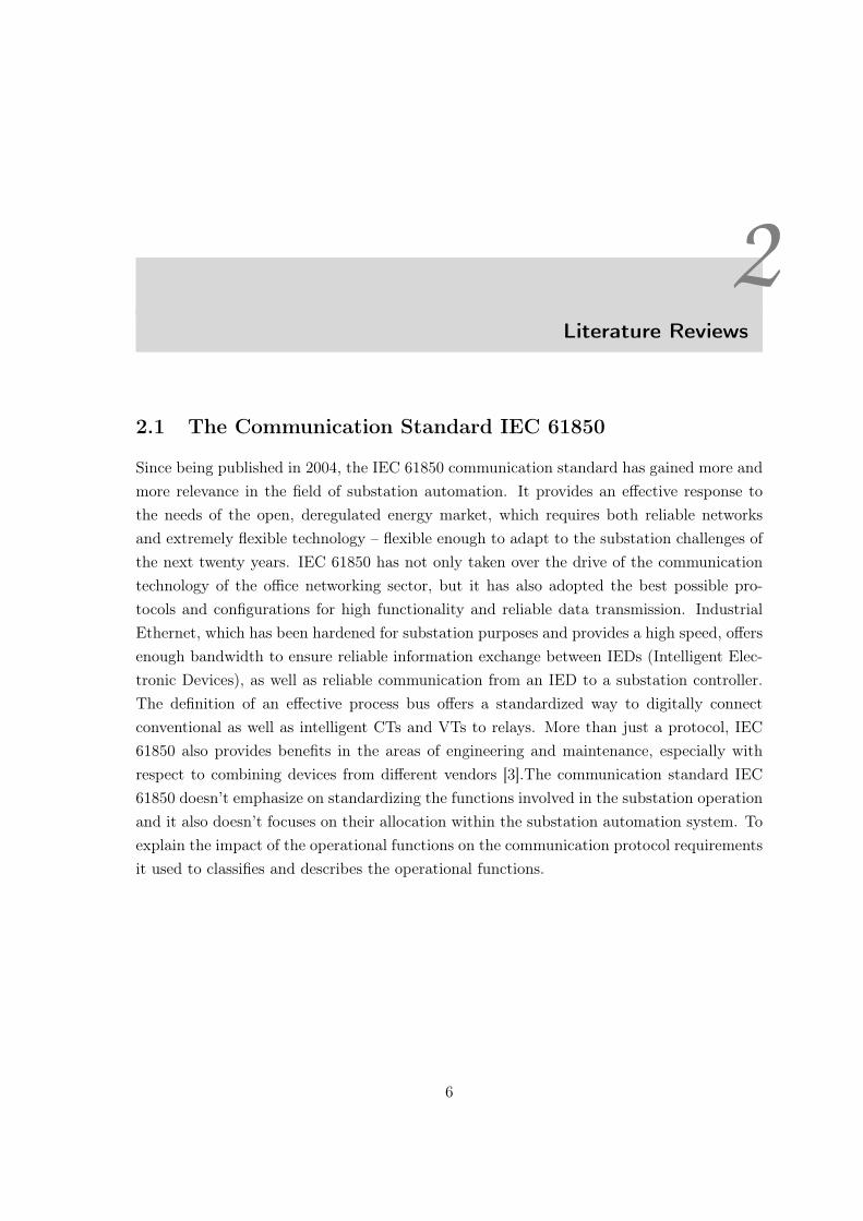
2.1 The Communication Standard IEC 61850
Since being published in 2004, the IEC 61850 communication standard has gained more andmore relevance in the field of substation automation. It provides an effective response tothe needs of the open, deregulated energy market, which requires both reliable networksand extremely flexible technology – flexible enough to adapt to the substation challenges ofthe next twenty years. IEC 61850 has not only taken over the drive of the communicationtechnology of the office networking sector, but it has also adopted the best possible pro-tocols and configurations for high functionality and reliable data transmission. IndustrialEthernet, which has been hardened for substation purposes and provides a high speed, offersenough bandwidth to ensure reliable information exchange between IEDs (Intelligent Elec-tronic Devices), as well as reliable communication from an IED to a substation controller.The definition of an effective process bus offers a standardized way to digitally connectconventional as well as intelligent CTs and VTs to relays. More than just a protocol, IEC61850 also provides benefits in the areas of engineering and maintenance, especially withrespect to combining devices from different vendors [3].The communication standard IEC61850 doesn’t emphasize on standardizing the functions involved in the substation operationand it also doesn’t focuses on their allocation within the substation automation system. Toexplain the impact of the operational functions on the communication protocol requirementsit used to classifies and describes the operational functions.
6

Figure 2.1: Substation Automation with IEC 61850[23]
2.1.1 Scope and Outline of IEC 61850
The table2.1 defines the various aspects of the substation communication network in 10major sections [2]. Parts 3, 4, and 5 of the standard describe the general and specificfunctional requirements for communications in a substation such as High-speed IED toIED communication, Networkable throughout the utility enterprise, High-availability, Multi-vendor interoperatibility, Voltage and current samples data support, configuration support,support for security etc.These requirements are then used as forcing functions to aid inthe identification of the services and data models needed, application protocol required,and the underlying transport, network, data link, and physical layers that will meet theoverall requirements. IEC 61850-6 specifies a description language for the configurationof electrical substatios related to IEDs. This language is called Substation Configurationdescription Language (SCL). It is used to describe IED configurations and communicationsystems according to IEC 61850-5 and IEC 61850-7-x. It allows the formal description of therelations between the substation automation system and the substation. At the applicationlevel, the switchyard topology itself and the relation of the switchyard structure to the SASfunctions (logical nodes) configured on the IEDs can be described. This communicationprotocol standard implements "abstracting" the definition of the data items and the services,this is the most important architectural concept of this protocol standard. It means thisstandard creates data objects and services that are independent of any underlying protocols.
7

Then "mapping" of the data objects and services to any other protocol that can meet thedata and service requirements allows by the abstract definition. Part 7.2 of the standarddescribe the definition of abstract and 7.4 define the abstraction of the logical nodes. Section7.3 describes the model of “ Common Data Classes ”, which defined common building blocksfor creating the larger data objects.
Part# Title
1 Introduction and Overview
2 Glossary of terms
3 General Requirements
4 System and Project Management
5 Communication Requirements for Functions and Device Models
6 Configuration Description Language for Communication in Electrical Substa-tions Related to IEDs
7 Basic Communication Structure for Substation and Feeder Equipment
7.1 - Principles and Models
7.2 - Abstract Communication Service Interface (ACSI)
7.3 - Common Data Classes (CDC)
7.4 - Compatible logical node classes and data classes
8 Specific Communication Service Mapping (SCSM)
8.1 - Mappings to MMS(ISO/IEC 9506 – Part 1 and Part 2) and to ISO/IEC8802-3
9 Specific Communication Service Mapping (SCSM)
9.1 - Sampled Values over Serial Unidirectional Multidrop Point-to-Point Link
9.2 - Sampled Values over ISO/IEC 8802-3
10 Conformance Testing
Table 2.1: Structure of The IEC 61850 Standard
The purpose of section 8 is to provide detailed specifications as to the mechanisms andrules required to implement the services, objects, and algorithms specified in IEC 61850-7-2,IEC 61850- 7-3, and IEC 61850-7-4 while making use of Web services and other applicationprotocols [2] .Mapping of the sampled values over serial unidirectional multidrop point-to-point to an Ethernet data frame is described in the section 9.1. IEC 61850-10 specifies stan-dard techniques for testing of conformance of client, server and sampled value devices andengineering tools, as well as specific measurement techniques to be applied when declaringperformance parameters. The use of these techniques will enhance the ability of the systemintegrator to integrate IEDs easily, operate IEDs correctly, and support the applications as
8

intended.
2.1.2 Logical Nodes
Although a server is a physical device, it is constructed with virtual data object [19].A setof logical device uses to fabricate an IEC 61850 server within an IED. Logical device is acollection of Logical nodes(LN) for performing specific function within IED. LN is a data setmentioned by IEC 61850 to define the information object of a function or device how it willbe communicated in a substation. In substation automation system LN uses for providinga unique identification of each logical device. According to the standard LNs are consideredas data producer and consumer.
Outputs
Sig
nalin
g A
dap
tion
Fixed Logic
Editable Logic
Logic
Inputs
Settings Controls
Figure 2.2: Structure of an IEC 61850 logical Node
An architecture of IEC 61850 logical node shown in figure 2.2 takes input and providean output processed by logic unit. Each logical node has two layers. The fist layer describessemantics of LN and second layer contains the logic unit which decides functionality ofthe LN. Every logic unit has both fixed and editable logic. Logics set by manufactureris referred as fixed logic e.g protection logic, which are IED and design specification forsubstation system. On the other hand, editable logic can be modified by end user to addflexibility that is lacking in LN.
2.1.3 Benefits of IEC 61850
The standard IEC 61850 has several benefits in the substation communication system [2].This is a unique standard. Design, build, install, commission and operate the power systemhas become more cost effective because of these unique characteristics of IEC 61850. This
9

communication protocol standard has developed a fundamental positive impacts on the sub-station automation system that is not possible in the time when engineers used to approachlegacy communication protocols. Some of the major benefits of IEC 61850 are stated below,
• This standard ensure high level services.
• Standardized Configuration language
• IEC 61850 devices are self describing.
• Makes the installation cost lower.
• Lower transducer cost.
• This standard are able to deliver data without re-configuring a device.
• Implement new capabilities.
2.2 Rule Based System
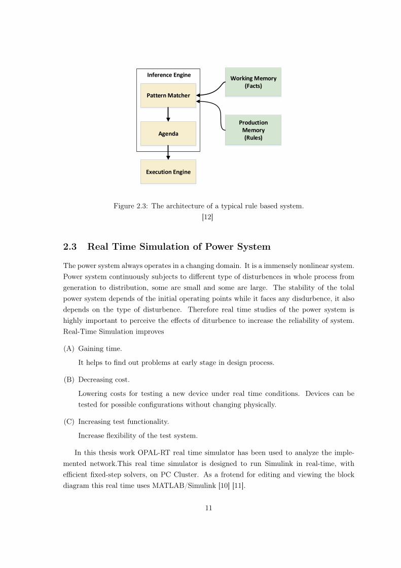
"A rule based system is a system that uses rules to drive conclusions from premises. It mustbe executed by some kind of runtime system that understands how to fill in the blanks anduse the declarative information to solve problems. Because declarative programs includeonly the important details of a solution, they can be easier to understand than proceduralprograms" [12]. Java expert system shell(Jess)has been used in this project to develop rulesfor the distribution network. Jess is a type of rule based system is made up of individualrules instead of forming a long sequence of instructions. A rule a kind of instruction that canbe executed in certain situation by the rule engine. Rule engine determine which rule shouldbe executed for any given situation or time. Figure 2.3 describes a typical architecture ofa rule based system. Where rule applies in the rule base by pattern matcher to the factscontaining in the working memory to create the agenda. The pattern matcher and agendatogether known as Interface engine. Execution engine fires the rule from agenda and refreshthe working memory to start a new cycle [12].
10
Pattern Matcher
Agenda
Execution Engine
Working Memory(Facts)
Production Memory(Rules)
Inference Engine
Figure 2.3: The architecture of a typical rule based system.[12]
2.3 Real Time Simulation of Power System
The power system always operates in a changing domain. It is a immensely nonlinear system.Power system continuously subjects to different type of disturbences in whole process fromgeneration to distribution, some are small and some are large. The stability of the tolalpower system depends of the initial operating points while it faces any disdurbence, it alsodepends on the type of disturbence. Therefore real time studies of the power system ishighly important to perceive the effects of diturbence to increase the reliability of system.Real-Time Simulation improves
(A) Gaining time.
It helps to find out problems at early stage in design process.
(B) Decreasing cost.
Lowering costs for testing a new device under real time conditions. Devices can betested for possible configurations without changing physically.
(C) Increasing test functionality.
Increase flexibility of the test system.
In this thesis work OPAL-RT real time simulator has been used to analyze the imple-mented network.This real time simulator is designed to run Simulink in real-time, withefficient fixed-step solvers, on PC Cluster. As a frotend for editing and viewing the blockdiagram this real time uses MATLAB/Simulink [10] [11].
11

2.4 Structure of Wind Solar Distributed Power System
Shortage of energy and environmental pollution leading power system towards integration ofmore and more renewable energy such as bio-energy, solar energy, wind power, wave energy,terrestrial heat energy, and hydrogen energy and so on[8]. The research of distributed powersystem with the solar and wind power are the most focused sectors. Electricity generationby wind power and solar cell are depends on the condition of weather, they do not supplythe steady electricity.
Wind Turbine
DC/DC
AC/DCG
DC/DCSolar Cell
Load
Controller
Bus
Figure 2.4: Wind-Solar Distributed Power System[8]
The output power of wind generation can be calculated by the following equation,
Pavail =12ρAv
3Cp
Where Cp is the power coefficient. The maximum value of power coefficient of any designof wind turbine is 0.59. It has been observed in different studies that for the maximum valueofCp the ration between the wind speeds and the rotor speeds of the wind turbine is constantat value 9. So it can be said that for achieving high-power efficiency at different wind speed,the rotor speed of the turbine has to adjust continuously against wind speed.
Efficiency of a solar cell measured by the ability of converting solar energy into usablepower. It can be represented by the following equation,
12
ηmax = PmaxESWSγ ×Ac
ESWSγ defines the incident radiation flux, that is the amount of sunlight that hits theearth’s surface in W/m2.
2.5 The Standard IEC 61175
The standard IEC 61175 proposed by technical committee(IEC/TC:3)of International Elec-trotecnial Commission in May 2013 [13]. In this report edition 3 of this standard has takento describe.The Rules and principals described in edition 1 and 2 proposed to be consideras part 1 by IEC/TC:3, This part describe the basic rules.The purpose of this standard isthe designation of signals in industrial systems, installations and equipment and industrialproducts. In this new edition of the standard, some references and descriptions are added todescribe how the signal designation is related to the information in the concept of numericalcommunication. The communication protocol standard IEC 61850 has been considered forthe numerical communication as an example.
2.5.1 Structure of IEC 61175
IEC 61175 standard divided into eight parts. First three parts describes scope, normativereferences, terms and definition respectively[13]. From fourth to eighth, each part is dividedinto three subsection. In the fourth part Basic principles of signal transfer, naming, signalclassification, signal name domain are described. "Designation of signals" is the Part five ofIEC 61175 standard, this part narrates the structure of the signal designation, recommendedcharacters for naming signals and forming signal designation. Part six of this standard saysabout the identification of signals in the signal connection network. This part also describethe packing of signals in signal carrier medium and grouping of signal with the purpose ofcommon presentation. When signals travel from source to destination it may pass throughmany interfaces between system and components. In part seven, it is described how toidentify signals in interfaces for data exchange in a network. Part eight is the last part ofIEC 61175 standard. The main idea of this part is the presentation of signals in HMI(HumanMachine Interface) and in documents. This part also describe the presentation of meta-data for signals. The Standard IEC 61175 also has six Annex (A to F) added with thespecification.
2.5.2 General Concepts of Signal Designation
According to the IEC 61175 standard all signals are classified into two groups with respecttheir treatment in designation[13]. One is the group of reporting signals and another one isthe group of controlling signals. These classification has done on the basis of the information
13

flow between controlled and controlling object. The controlled object also known as "MainObject". The main object is the object where the main process takes place. For example, ifa circuit breaker has to control from a control panel then the main process will held in thecircuit breaker to close/open it. So here the circuit breaker will be considered as a "MainObject".
Controlling Object Controlled Object
Controlling Signals
Reporting Signals
Figure 2.5: Relation between Controlling and reporting signal
The signal groups further split into signal classes. According to the IEC 61175 signalsare categorized into eight classes, such as Alarm signal, Command, Event signal, Indicationsignal, Power supply, Measuring signals, Setting Value and Additional Classes. Each classcan be represented by a latter code given in the specification of the standard(Shown in table2.2).The group of reporting signals contains alarm, indication, event, measuring, powersupply etc. On the other hand the group of controlling signals contains command signal,setting value signal etc.
Signal Class Code Signal ClassA Alarm SignalC CommandE Event SignalI Indication SignalL Power SupplyM Measuring SignalS Setting ValueX Additional Class
Table 2.2: Letter Codes for signal class[13].
Signal name should be unambiguous in the signal name domain[13]. It means eachsignal will have only one interpretation in the same domain. Signal domain can contains
14
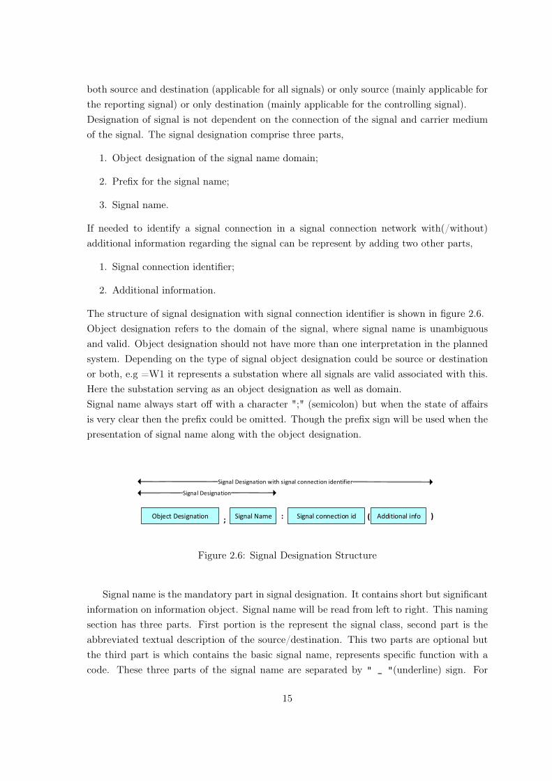
both source and destination (applicable for all signals) or only source (mainly applicable forthe reporting signal) or only destination (mainly applicable for the controlling signal).Designation of signal is not dependent on the connection of the signal and carrier mediumof the signal. The signal designation comprise three parts,
1. Object designation of the signal name domain;
2. Prefix for the signal name;
3. Signal name.
If needed to identify a signal connection in a signal connection network with(/without)additional information regarding the signal can be represent by adding two other parts,
1. Signal connection identifier;
2. Additional information.
The structure of signal designation with signal connection identifier is shown in figure 2.6.Object designation refers to the domain of the signal, where signal name is unambiguousand valid. Object designation should not have more than one interpretation in the plannedsystem. Depending on the type of signal object designation could be source or destinationor both, e.g =W1 it represents a substation where all signals are valid associated with this.Here the substation serving as an object designation as well as domain.Signal name always start off with a character ";" (semicolon) but when the state of affairsis very clear then the prefix could be omitted. Though the prefix sign will be used when thepresentation of signal name along with the object designation.
Object Designation ; Signal Name Signal connection id: ( )Additional info
Signal Designation
Signal Designation with signal connection identifier
Figure 2.6: Signal Designation Structure
Signal name is the mandatory part in signal designation. It contains short but significantinformation on information object. Signal name will be read from left to right. This namingsection has three parts. First portion is the represent the signal class, second part is theabbreviated textual description of the source/destination. This two parts are optional butthe third part is which contains the basic signal name, represents specific function with acode. These three parts of the signal name are separated by " _ "(underline) sign. For
15

example ;M_VT1_UL1 here M is the measurement class, VT1 is voltage transformer 1 andthe measurement is voltage(U) from phase one (L1).The structure of the signal name isshown in figure 2.7.
Signal Class _ Short Name Basic Signal Name_
Signal Name
Figure 2.7: Structure of the signal name
Signal connection identifier which is illustrated in figure 2.8) is separated from the signaldesignation by " : " (colon) sign. This is an optional part in signal designation. Thissection of the signal designation mainly describe at which connection point signal interfacedto object in network.
;I_CB1_Close:3
;I_CB1_Close:4
;I_CB1_Close:2 ;I_CB1_Close:1
Event Recorder
Indication Panel
Cubicle 2Cubicle
1
Circuit Breaker 1
Signal interface to object
Figure 2.8: Signal connection identifier
This is an optional part in general but must be added when signal is transferred:
• From one system to another
16

• From one component to another
• From one signal connection medium to another
• From one source to different source
If any additional information need to provide in a signal designation then that could berepresent in by putting a "(...)" sign. This additional information could be alternativelyname or other information related to the packaging of the information object for transfer-ring,Other system information i.e. protocol related parameter,data related to the signaltransmission etc.
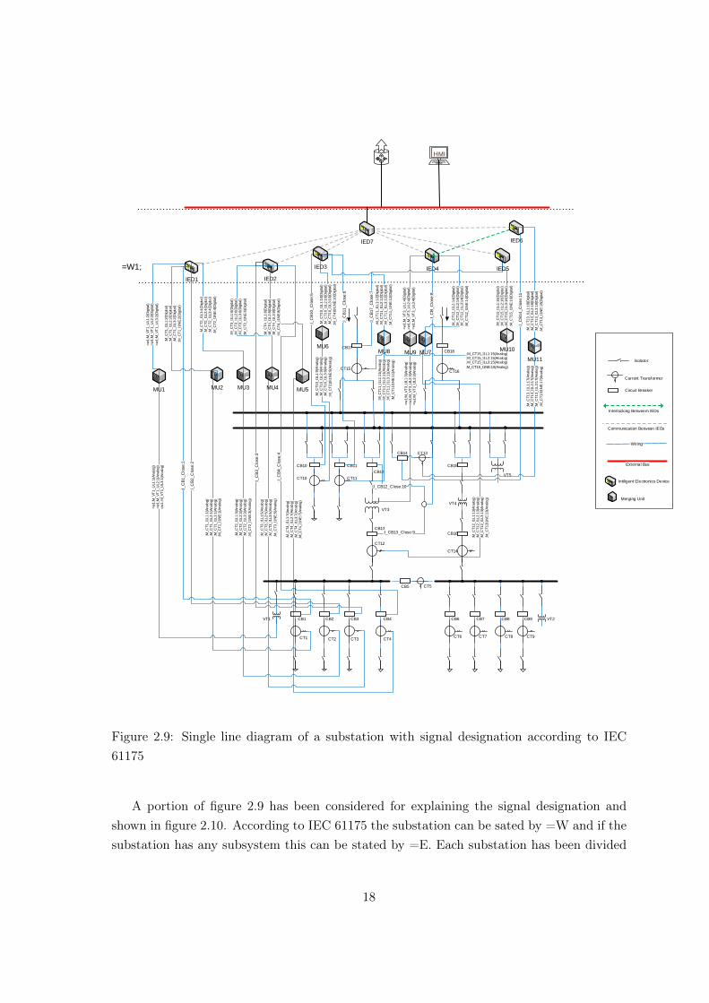
The Figure 2.9 shows a single line diagram of substation automation done according tocommunication protocol standard IEC 61850. In this diagram all connections considered asthree phases.
17
CB18
CT16
CB17
CT15
CT11
CB11
CB12
VT3
CB13
CT12
CB15
VT4
CB16
CT14
CB14 CT13
CB5 CT5
CB10
CT10
CB2
CT2
CB3
CT3
CB4
CT4
CB6
CT6
CB7
CT7
CB8
CT8
CB9
CT9
VT5
VT2
IED1
MU1
;M_C
T4_I1
L1:7
(An
alo
g)
;M_C
T4_I1
L2:7
(An
alo
g)
;M_C
T4_I1
L3:7
(An
alo
g)
;M_C
T4_I1
NE
:7(A
na
log)
IED2
Interlocking Betweem IEDs
Communication Between IEDs
Wiring
External Bus
Circuit Breaker
Current Transformer
Intiligent Electronics Device
Merging Unit
Isolator
MU2 MU3
;M_C
T2_I1
L1:3
(An
alo
g)
;M_C
T2_I1
L2:3
(An
alo
g)
;M_C
T2_I1
L3:3
(An
alo
g)
;M_C
T2_I1
NE
:3(A
na
log)
;M_C
T3_I1
L1:5
(An
alo
g)
;M_C
T3_I1
L2:5
(An
alo
g)
;M_C
T3_I1
L3:5
(An
alo
g)
;M_C
T3_I1
NE
:5(A
na
log)
MU4 MU5
;I_
CB
2_
Clo
se
:2
=w
1;M
_V
T1_U
L1:2
(Dig
ital)
=w
1;M
_V
T1_U
L2:2
(Dig
ital)
=w
1;M
_V
T1_U
L3:2
(Dig
ital)
;M_C
T2_I1
L1:4
(Dig
ital)
;M_C
T2_I1
L2:4
(Dig
ital)
;M_C
T2_I1
L3:4
(Dig
ital)
;M_C
T2_I1
NE
:4(D
igita
l)
;M_C
T3_I1
L1:6
(Dig
ital)
;M_C
T3_I1
L2:6
(Dig
ital)
;M_C
T3_I1
L3:6
(Dig
ital)
;M_C
T3_I1
NE
:6(D
igita
l)
;M_C
T4_I1
L1:8
(Dig
ital)
;M_C
T4_I1
L2:8
(Dig
ital)
;M_C
T4_I1
L3:8
(Dig
ital)
;M_C
T4_I1
NE
:8(D
igita
l)
;I_C
B3
_C
lose:3
;I_C
B4
_C
lose
:4
IED3 IED4
;M_C
T1
0_I1
L1:9
(An
alo
g)
;M_C
T1
0_I1
L2:9
(An
alo
g)
;M_C
T1
0_I1
L3:9
(An
alo
g)
;M_C
T2
10I1
NE
:9(A
na
log)
MU6
;M_C
T1
0_I1
L1:1
0(D
igita
l);M
_C
T1
0_I1
L2:1
0(D
igita
l);M
_C
T1
0_I1
L3:1
0(D
igita
l)
;M_C
T4
10I1
NE
:10(D
igita
l)
;I_
CB
10
_C
lose
:5
;M_C
T1
1_I1
L1:1
1(A
na
log)
;M_C
T1
1_I1
L2:1
1(A
na
log)
;M_C
T1
1_I1
L3:1
1(A
na
log)
;M_C
T1
1I1
NE
:11(A
na
log)
MU8
;M_C
T1
1_I1
L1:1
2(D
igita
l);M
_C
T1
1_I1
L2:1
2(D
igita
l);M
_C
T1
1_I1
L3:1
2(D
igita
l)
;M_C
T1
1_I1
NE
:12(D
igita
l)
MU9
=w
1;M
_V
T3_U
L1:3
(An
alo
g)
=w
1;M
_V
T3_U
L2:3
(An
alo
g)
=w
1;M
_V
T3_U
L3:3
(An
alo
g)
=w
1;M
_V
T3_U
L1:4
(Dig
ital)
=w
1;M
_V
T3_U
L2:4
(Dig
ital)
=w
1;M
_V
T3_U
L3:4
(Dig
ital)
;I_
CB
11
_C
lose
:6
;I_CB13_Close:9
;I_C
B_C
lose:8
;I_CB12_Close:10
;I_
CB
17
_C
lose
:7
MU10;M_CT15_I1L1:15(Analog);M_CT15_I1L2:15(Analog);M_CT15_I1L3:15(Analog)
;M_CT15_I1NE:15(Analog)
;M_C
T1
5_I1
L1:1
6(D
igita
l);M
_C
T1
5_I1
L2:1
6(D
igita
l);M
_C
T1
5_I1
L3:1
6(D
igita
l)
;M_C
T1
5_I1
NE
:16(D
igita
l)
IED5
MU7
;M_C
T1
2_I1
L1:1
3(A
na
log)
;M_C
T1
2_I1
L2:1
3(A
na
log)
;M_C
T1
2_I1
L3:1
3(A
na
log)
;M_C
T1
2I1
NE
:13(A
na
log)
;M_C
T1
2_I1
L1:1
4(D
igita
l);M
_C
T1
2_I1
L2:1
4(D
igita
l);M
_C
T1
2_I1
L3:1
4(D
igita
l)
;M_C
T1
2_I1
NE
:14(D
igita
l)
IED6
;M_C
T1
3_I1
L1:1
7(A
na
log)
;M_C
T1
3_I1
L2:1
7(A
na
log)
;M_C
T1
3_I1
L3:1
7(A
na
log)
;M_C
T1
3I1
NE
:17(A
na
log)
MU11
;M_C
T1
3_I1
L1:1
8(D
igita
l);M
_C
T1
3_I1
L2:1
8(D
igita
l);M
_C
T1
3_I1
L3:1
8(D
igita
l)
;M_C
T1
3_I1
NE
:18(D
igita
l)
;I_
CB
14
_C
lose
:11
IED7
HMI
=W1;
CB1
CT1
VT1
=w
1;M
_V
T1_U
L1:1
(An
alo
g)
=w
1;M
_V
T1_U
L2:1
(An
alo
g)
=w
1.;M
_V
T1_U
L3:1
(An
alo
g)
;M_C
T1_I1
L1:1
(An
alo
g)
;M_C
T1_I1
L2:1
(An
alo
g)
;M_C
T1_I1
L3:1
(An
alo
g)
;M_C
T1_I1
NE
:1(A
na
log)
;I_
CB
1_
Clo
se
:1
;M_C
T1_I1
L1:2
(Dig
ital)
;M_C
T1_I1
L2:2
(Dig
ital)
;M_C
T1_I1
L3:2
(Dig
ital)
;M_C
T1_I1
NE
:2(D
igita
l)
Figure 2.9: Single line diagram of a substation with signal designation according to IEC61175
A portion of figure 2.9 has been considered for explaining the signal designation andshown in figure 2.10. According to IEC 61175 the substation can be sated by =W and if thesubstation has any subsystem this can be stated by =E. Each substation has been divided
18

into several bays and the bay can be represented by =Q (If any substation contains morethan one bay then a number should be added e.g. =Q1, =Q2,...). Voltage transformer,current transformer, circuit breaker can be represented by VT, CT and CB respectively.
CB1CT1
VT1
=W1.Q1;M_VT1_UL1:1(Analog)
=W1.Q1;M_VT1_UL2:1(Analog)
=W1.Q1.;M_VT1_UL3:1(Analog)
=W1.Q1;M_CT1_I1L1:1(Analog)
=W1.Q1;M_CT1_I1L2:1(Analog)
=W1.Q1;M_CT1_I1L3:1(Analog)
=W1.Q1;M_CT1_I1NE:1(Analog)
=W1.Q1;I_CB1_Close:1
=W1.Q1;M_CT1_I1L1:2(Digital)
=W1.Q1;M_CT1_I1L2:2(Digital)
=W1.Q1;M_CT1_I1L3:2(Digital)
=W1.Q1;M_CT1_I1NE:2(Digital)MU2
MU1
=W1Q1;M_VT1_UL1:2(Digital)
=W1.Q1;M_VT1_UL2:2(Digital)
=W1.Q1;M_VT1_UL3:2(Digital)
IED1
=Q1;
HMI
=W1;
=W1.Q1.CB1;C_CB_Close:1
Figure 2.10: A bay of the substation mentioned in figure 2.9
It is not mandatory to mention the bay or subsystem in signal naming when the signal isnot changing the subsystem, . But when the signal transfer from one bay to another bay orsubsystem then the bay/subsystem’s name should be included in the signal designation. Herein this Figure 2.10 CT1 sending all current measurements(I1) from 3 phases (L1, L2, L3)and neutral earthing (NE) to IED1 via MU2 (Merging unit(MU) act as an A/D converter).The signal for this path can be can be presented by =W1.Q1;M_CT1_I1L1. If needed, circuitbreaker cab be controlled by IED. In this example it is assumed that circuit break CB1is closed. This command from IED1 to CB1 can represent by =W1.Q1.CB1;C_CB_Close:1,where =W1.Q1.CB1 is the destination domain and this signal belong to the command class C.After implementing the command circuit breaker CB1 has sent an indication signal back toIED1 about its status and it has represented in the figure 2.10 by =W1.Q1;I_CB1_Close:1
and this signal belongs to Indication class(I). All the circuit breaker operate in either closeor open state depending on the situation. All voltage measurements (U) from three phases(L1,L2,L3) of VT1 also belongs to the measurement class as CT1 could be explained inthe same way as CT1 for example voltage measurement of phase one can be represented as=W1.Q1;M_VT1_UL1. The standard IEC 61175 also has specification for wiring and buses.
19
Electric wiring related to the main process and connection of the power supply can representby "Blue" colour. Internal bus such as internal communication path in controlling deviceis represented by "Black" lines. The external bus, by which controlling device exchangedata with the other device such as HMI can be modelled with "Red" line. In external businformation object will be presented as a package for purpose and at the receiving end thatpackage will be presented as individual information object.
2.5.3 Grouping of Signals
Signals may be organized in groups for different purposes. One reason is to make thecommunication easier in the signal connection network. It can be done by transmittingsignals as a package to receiving end where it will be unpacked as individual signal includingthe same information as used in the packing. In this case a new signal will be designatedwhich will contains identified information object and has their own signal designation as apart of the package.Data object needs an identifier, which can be done by adding a commonname for the package. For example
=W4.Q3;M_CT2_I1L1:4=W4.Q3;M_CT2_I1L2:5=W4.Q3;M_CT2_I1L3:6
if these signals require packing in signal carrier medium can be represented as
=W4.Q3;M_CT2_I1 :1
Signals may be grouped also for common presentation. In this case a new signal hasto create with their with its own signal designation, which contains the information objectsfrom the grouped signals.But packaged signas cannot be identified individully at the recevingend.
20

3The Reference Network
3.1 Introduction
The distribution system works as a bridge between the utility and customers [3]. Dependingon load density and system voltage level electricity distribution network can be designed indifferent ways for different areas. To perform this thesis work a mesh distribution networkhas been selected. The mesh arrangement frequently used in HV system as interconnectingcircuits of the mesh arrangement can provide increased security of supplies to individualsubstation. While this arrangement requires more substation equipment overall, for exampleswitchgear and electrical connections, it is usually more efficient in terms of total circuitcosts. The mesh arrangement is easier to extend and has a higher utilizations of circuitswhen fully developed than a ring system, although this is can result in a higher networklosses [4].This chapter intends to provide a brief description and discussion of the selected meshdistribution network RBTS (R.Billinton Test System) bus 4.
3.2 IEEE RBTS Bus 4 Distribution System
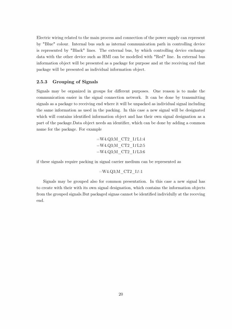
Reliability test system has been used widely over the years by researcher,as a benchmarkto develop and compare probabilistic reliability evaluation methods.One of the most usedsystem for reliability testing is RBTS [5] [6]. It was developed at University of Saskatchewanfor educational purposes and research. Figure 4.1 show the result which investigated theRBTS used for different type of reliability studies. Depending on different characteristicsof reliability analyses of power system the figure has been divided into following sectionsstated below,
(A) Reliability analysis and Planning of generation end.
(B) Reliability analysis and Planning of transmission system.
21
(C) Economics analysis of the power system and Optimization.
(D) Reliability analysis and Planning at Distribution end.
(E) Finding new techniques for reliability analysis in power system.
Figure 3.1: The RBTS used for different type of reliability studies.
It can be observed from the figure 4.1 almost 80% of the studies of reliability analysis andnew techniques finding for reliability analysis used the RBTS as reference model[5]. So itcan be said that the RBTS bus 4 distribution network is the perfect selection for performingthis thesis work.
RBTS bus 4 arrangement shown in figure 2.5 has three voltage levels 33 kV, 11 kV and400 v. It also has four ring linking bus bars around the distribution network are belongto 33 kV voltage level. Distribution network belong to 11 kV and 400 V Voltage level issupplied through 7 feeders point via six 33/11 kV transformers. It is assumed 33 kV feederside has 100% reliability. Total system has residential consumers,commercial consumers,government/institution consumers and small users. All of the small users connected to highvoltage side are directly supplied by 11 kv feeders on the other hand residential,commercialand government/institution consumers connceted to low voltage side are supplied via 11kV/425 V transformers. This RBTS bus 4 network has been designed for 4779 consumerswhich are connected to the network at 38 load points [6][7].
22

SP1-F1
F1-D1
SP1-F3
F3-D1
F2-D1
F2-D2F2-D3
F1-D3
F1-D2
F1-D4
F1-D5
F3-D3F3-D2
F3-D5
F3-D4
F7-D4
F7-D2
F7-D3
F7-D1
SP3-F7
SP3-F6
F6-D2
F4-D5
F4-D3
F4-D4
SP2-F4
F4-D2
SP2-F5
F4-D1
F6-D1
F5-D1
F5-D2
SP1-F2
F5-D4 F5-D3
F6-D3
F7-D5
L1
L2
L3
L4
L5
L6L7
L8
L9
L10
L11
L12
L13
L14
L15
L16
L17
L18
L19
L20
L21
L22
L23 L24
L25
L26
L27
L28
L29
L30
L31
L32L33
L34
L35
L36 L37
L38
33 kV
11 kV
Figure 3.2: Distribution Network for RBTS Bus 4
Without connecting the dotted lines (figure 4.2)all the feeders operated as redial feed-ers.According to the RBTS bus4 specification it is allowed to connect the dotted lines totransform the distribution network from radial to mesh and consumer to be supplied fromalternative supply points. It also has been considered all the breakers in the network areidentified and all the 11 kV feeder are either overheard lines or cables [7].
23

4Implementation
4.1 Introduction
This chapter outlines the total implementation process which includes the reference networkimplementation, Signals mapping to the RT lab OPC server, algorithm design for Signalparsing in Java and integration of Jess rule engine. Ontology development in JADE willalso be discussed in this chapter.
4.3 Network Modelling
4.3.1 Implementation of RBTS bus-4 network4.3.2 Distributed generation profile4.3.3 Estimated consumer and load profile4.3.4 Modelling for RT-Lab simulator
4.4 Signal Modelling
4.4.1 Naming of substation4.4.2 Naming of power transformer4.4.3 Naming of DG units4.4.4 Naming of signals in reference network
4.3 Implementation of signal parser in Java
4.4 Implementation of rules in Jess
4.5 Jade ontology development
Table 4.1: Structure of this chapter
24

4.2 Implementation Phases
The implementation process of this thesis work has been divided into three steps, illustratedin figure 4.1.
In fist step, reference network is modelled in real time simulator OPAL-RT and mappedall the signals to RT-lab server. In this phase all the signal named according the designationstandard IEC 61175. For signal mapping a Java Application Programming Interface hasdeveloped to get all the signals from the RBTS network to OPC server.
In second step, a Java program is developed to parse all the signals fetched from thedistribution network. This step also includes a Jess application for checking whether themeasured real time data is acceptable or not and generate an alarm and for calculating thegeneration of DG.
In third phase, Graphical user interface (GUI) is designed to have a clear view of theentire distribution system.
OPC Server
Signal Naming according to IEC 61175
This programm contains a Client
implemented in JAVA and an algorithom in
JESS rule engine.
GUI
This will show the total Distribution network in a tree
format.
Figure 4.1: Steps of Implementation
25
4.3 Network Modelling
4.3.1 Implementation of the RBTS Bus 4 Network
A smart distribution system can be planned in many ways such as applying the idea ofMicro grid to the system, distributed automation, distributed generation (DG) etc. In thisthesis work concept of DG has been applied to make the RBTS bus 4 distribution modelmore efficient. DG refers to small scale power generation at the point of consumption. Overthe past few decades penetration of DG in distribution system is increasing. Generatingpower on site has many benefits rather than generating centrally. DG reduce costs, increaseefficiency of the system, decrease interdependency and reduce complexity [8][9].As this workintended to perform on a mesh network the dotted lines are connected which is presentedin figure 4.2.
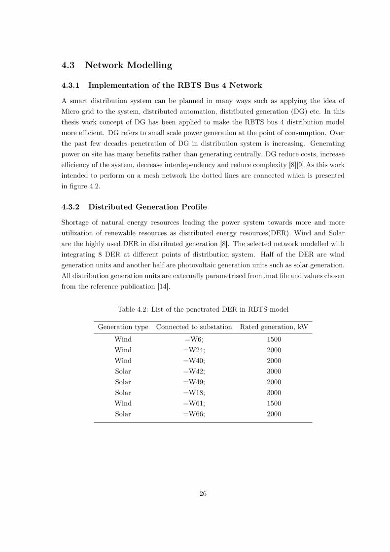
4.3.2 Distributed Generation Profile
Shortage of natural energy resources leading the power system towards more and moreutilization of renewable resources as distributed energy resources(DER). Wind and Solarare the highly used DER in distributed generation [8]. The selected network modelled withintegrating 8 DER at different points of distribution system. Half of the DER are windgeneration units and another half are photovoltaic generation units such as solar generation.All distribution generation units are externally parametrised from .mat file and values chosenfrom the reference publication [14].
Table 4.2: List of the penetrated DER in RBTS model
Generation type Connected to substation Rated generation, kW
Wind =W6; 1500Wind =W24; 2000Wind =W40; 2000Solar =W42; 3000Solar =W49; 2000Solar =W18; 3000Wind =W61; 1500Solar =W66; 2000
26

=W2;
=W21
;
=W14
; =W16
;=W
18;
=W6;
=W4;
=W8;
=W11
;
=W24
;=W
22;
=W29
;
=W27
;
=W64
;
=W59
;
=W61
;
=W58
;
SP3-
F7
SP3-
F6
=W53
;
=W42
;
=W37
;
=W40
;
SP2-
F4
=W34
;
SP2-
F5
=W33
;=W
52;
=W46
;
=W47
;
=W49
;
=W55
;
=W66
;
Dis
trib
ute
d
Gen
erat
ion
Un
it
Sub
stat
ion
Win
d G
en.
Win
d G
en.
Win
d G
en.
Win
d G
en.
Sola
r G
en.
Sola
r G
en.
Sola
r G
en.
Sola
r G
en.
=W1;
=W1;
=W1;
L11
L1
L8
L
L12
L17
L16 L2
3
L22
L27
L21
L2 L3L5
L7L6
L35
L36
L37 L3
2L3
3
L29
L38
L4
L31
L30
L28
L9
L19
L24
L15
L25
L14
L13
L18
L26
33kV
11kV
33kV
11kV
11kV
33kV
SP1-
F1SP
1-F2
SP1-
F3
L10
L20
L34
Figure 4.2: Distribution network for RBTS bus 4 modelled with DGs.
27

4.3.3 Estimated consumer and Load Profile
All the consumer and loading data chosen from the reference paper [7]. According to thereference [7], RBTS bus 4 distribution network has different type of consumer connectedat different end of bay. Total average value of load seen by the load point is 24.58 MW,due to variety between consumers and normal load level variation throughout a period. Forsystem analysis both dynamic and static loads are considered. Dynamic loads are externallyparametrised from .mat file. Customer and loading data for RBTS network presented intable4.3and in table4.4 respectively.
Table 4.3: Customer Data
[7].
Number ofload points
Load pointsCustomerType
Load level per load pointMW
Number ofcustomer
average peak15 1-4,11-13,18-21,32-35 residential 0.545 0.8869 2207 5,14,15,22,23,36,37 residential 0.500 0.8137 2007 8,10,26-30 small user 1.00 1.63 12 9,31 small user 1.50 2.445 17 6,7,16,17,24,25,38 commercial 0.415 0.6714 10
Total 24.58 40.00 4779
28

Table 4.4: Load Distribution Data[7]
Feeder Number load points feeder load , MW Number of customersaverage peak
F1 1-7 3.51 5.704 1100F2 8-9 3.5 5.705 3F3 11-17 3.465 5.631 1080
SP1 Total 10.475 17.040 2183
F4 18-25 4.01 6.518 1300F5 26-28 3.0 4.890 3
SP2 Total 7.01 11.408 1303
F6 29-31 3.5 5.705 3F7 32-38 3.595 5.847 1290
SP3 Total 7.095 11.552 1293
Bus 4 Total 24.58 40.00 4779
4.3.4 Network Modelling for RT-LAB Simulator
To implement a Simulink model for RT-LAB simulator need some modifications such asregrouping the model into calculation subsystem, placing OpComm communication block,taking step size into consideration and using delay block.
4.3.4.1 Separating into Subsystem
For using a simulink model in RT-Lab has to be grouped into console(SC_) and compu-tation subsystem(SM_ or SS_). In this simulator All connections between console andcomputation subsystems are replaced by the hardware communication links and RT-Labuses TCP/IP for communicating between these blocks.
4.3.4.2 opComm Block
OpComm block convey information to RT-Lab regarding the type and size of the signalbeing transferred from one subsystem to another.
29

Figure 4.3: opComm Block.
One opComm block has to be placed in the computation subsystem for receiving signalsasynchronously form the console block. In the model has more than one subsystem thenanother opComm block can be inserted for receiving real-time-synchronized signals fromother computation subsystems. One or more opcomm block can inserted in console blockfor receiving signals for the computation subsystem [18].
4.3.4.3 Step Size
RT-Lab real time simulation is based on discrete time steps. To provide an acceptable resultof power system analysis step size should be less or equal to 50 µs and for analysis of powerelectronics the step size can be set 100 µs.
4.4 Signal Modelling
4.4.1 Naming of Substation
Substations in RBTS bus 4 network categorized according to the voltage levels. Overall dis-tribution network classified into three groups of substation primary, secondary and tertiary.All the primary substations belong to 33 kV voltage level. Secondary substations are part of11 kv network and tertiary substations are associated with 400 V level. Entire network has3 primary substations and each substation equipped with two 33/11 kV transformer. Totalnetwork has 29 nodal points situated in 11 kV network, each of the nodal point consideredas secondary substation. Each load point deliberate as tertiary substation.
According to the standard IEC 61175 substation can be named with the = WX;. Whereprefix sign EQUAL "=" represents the substation as function aspect stated in IEC refer-ence designation standard IEC 61346-2 [15].If the system has more than one substation canbe represented by a number X. In this thesis work this number has been chosen by MAT-POWER 4.1 which is a MATLAB based power system simulation tool for solving optimalpower flow problems of transmission or distribution system. This tool is used in this projectto find out the nodal points of RBTS bus4 network. These nodal numbers are used fornumbering primary and secondary substations. For tertiary substation an arbitrary num-ber was chosen. Some examples are given, = W1; primary substation, = W4; secondary
30
substation and = W300; = W301; tertiary substation.
4.4.1.1 Naming of Substation elements
In IEC 61175 the concepts of naming the elements of a substation taken form IEC 61346.Each substation partitioned into bays. Bay can be indicated by =Q and by adding a numberafter letter. All the bays are modelled with current transformer, voltage transformer, circuitbeaker and disconnecter switch. In this project all are named according to the standard.For example current transformer CT1 , voltage transformer VT1, circuit beaker CB1 anddisconnecter switch QB1.
4.4.2 Naming of Power Transformer
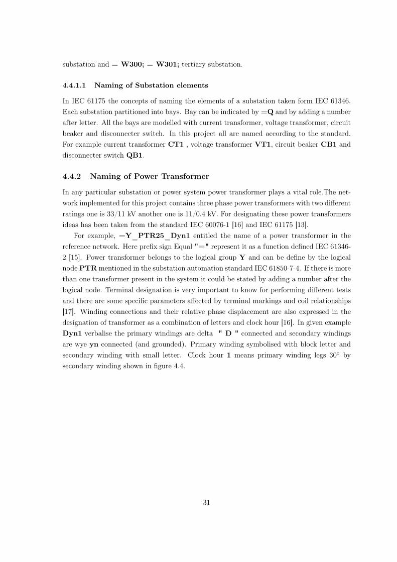
In any particular substation or power system power transformer plays a vital role.The net-work implemented for this project contains three phase power transformers with two differentratings one is 33/11 kV another one is 11/0.4 kV. For designating these power transformersideas has been taken from the standard IEC 60076-1 [16] and IEC 61175 [13].
For example, =Y_PTR25_Dyn1 entitled the name of a power transformer in thereference network. Here prefix sign Equal "=" represent it as a function defined IEC 61346-2 [15]. Power transformer belongs to the logical group Y and can be define by the logicalnode PTR mentioned in the substation automation standard IEC 61850-7-4. If there is morethan one transformer present in the system it could be stated by adding a number after thelogical node. Terminal designation is very important to know for performing different testsand there are some specific parameters affected by terminal markings and coil relationships[17]. Winding connections and their relative phase displacement are also expressed in thedesignation of transformer as a combination of letters and clock hour [16]. In given exampleDyn1 verbalise the primary windings are delta " D " connected and secondary windingsare wye yn connected (and grounded). Primary winding symbolised with block letter andsecondary winding with small letter. Clock hour 1 means primary winding legs 30◦ bysecondary winding shown in figure 4.4.
31

1 2 3
1 2 3
1
23
12
12
1
2
3
Dyn1
Figure 4.4: Illustration of ’clock number’ notation.
4.4.3 Naming of DG Units
The standard IEC 61850-7-4 is followed to name all the penetrated DG units to the RBTSbus-4 distribution network. It is already mentioned earlier entire network has eight DERand those are either solar or wind generation unit. According to the standard solar unit canbe represented by the logical group O and for wind it is W.e.g. =DER_O1 , =DER_W1 , Where DER symbolise as a Distributed energy resource.Since the network has more than one DG so it is represented by adding a number with thelogical group name.
4.4.4 Naming of signals in Reference Network
In this project only reporting signals has considered for naming. Due to the size of theimplemented network and some limitations RT-Lab simulator it was not possible to use anybreaker for performing this work. It is mentioned in OPAL-RT guide "If in one single topo-logically connected network model contains SPS switches (including circuit breakers, idealswitches, and other SPS power electronic switches but excluding Time-stamped bridges), it requires 2N cached switch pattern matrix permutations to hold the complete sets ofstate-space matrix". It is also stated any single topologically connected network can havemaximum 28 SPS switches for dynamic calculation otherwise it will be a cause of overrun.Separating the network into many subsystems was also not possible due to negligible com-munication delay in the distribution system and line length. Maximum line length for thisnetwork is 1 km. Three phase voltage and current measurement signals taken into account
32
and IEC 61175 followed for designation.
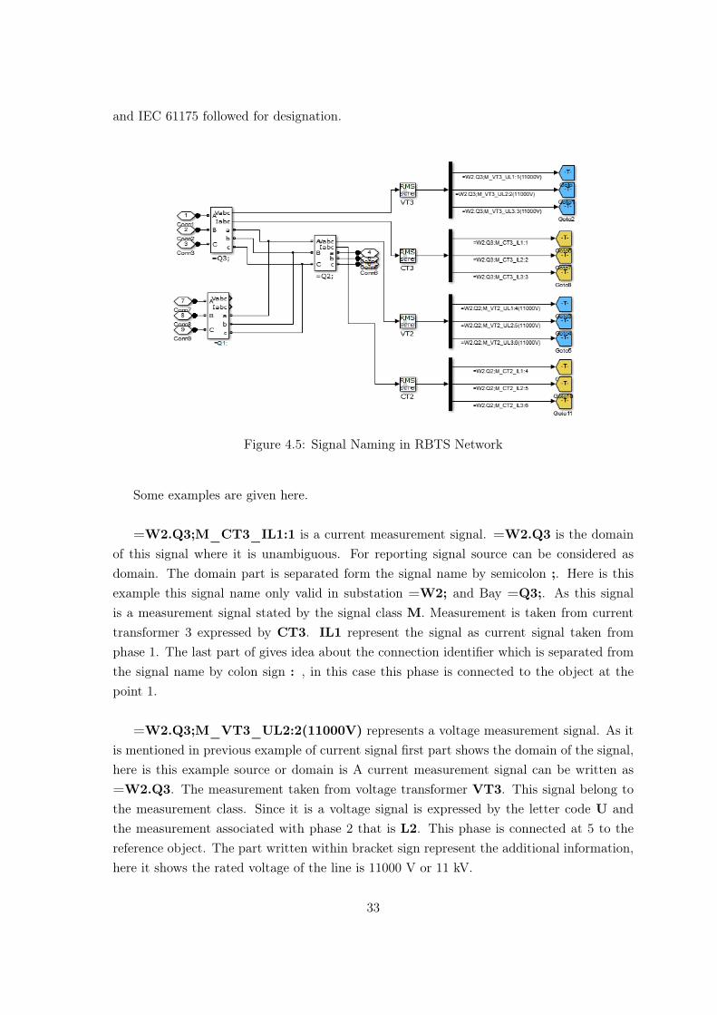
Figure 4.5: Signal Naming in RBTS Network
Some examples are given here.
=W2.Q3;M_CT3_IL1:1 is a current measurement signal. =W2.Q3 is the domainof this signal where it is unambiguous. For reporting signal source can be considered asdomain. The domain part is separated form the signal name by semicolon ;. Here is thisexample this signal name only valid in substation =W2; and Bay =Q3;. As this signalis a measurement signal stated by the signal class M. Measurement is taken from currenttransformer 3 expressed by CT3. IL1 represent the signal as current signal taken fromphase 1. The last part of gives idea about the connection identifier which is separated fromthe signal name by colon sign : , in this case this phase is connected to the object at thepoint 1.
=W2.Q3;M_VT3_UL2:2(11000V) represents a voltage measurement signal. As itis mentioned in previous example of current signal first part shows the domain of the signal,here is this example source or domain is A current measurement signal can be written as=W2.Q3. The measurement taken from voltage transformer VT3. This signal belong tothe measurement class. Since it is a voltage signal is expressed by the letter code U andthe measurement associated with phase 2 that is L2. This phase is connected at 5 to thereference object. The part written within bracket sign represent the additional information,here it shows the rated voltage of the line is 11000 V or 11 kV.
33
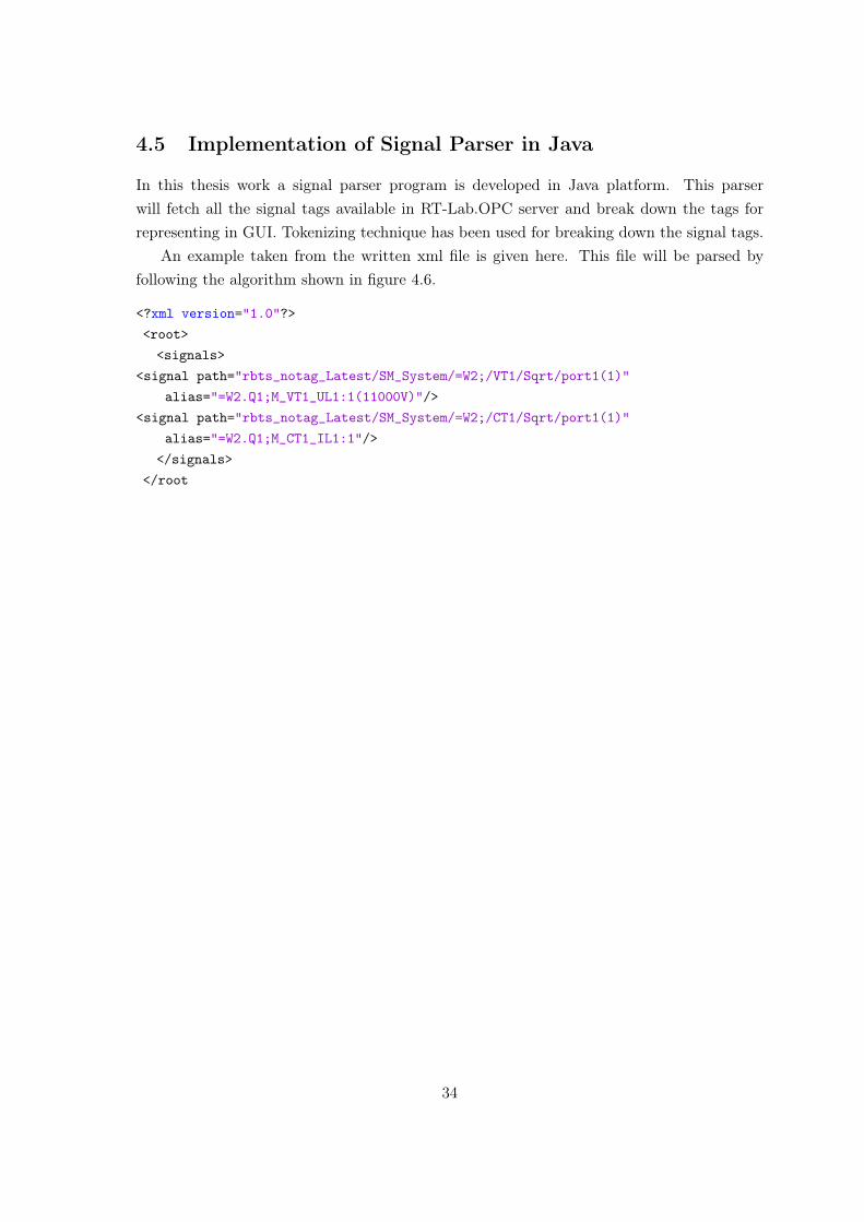
4.5 Implementation of Signal Parser in Java
In this thesis work a signal parser program is developed in Java platform. This parserwill fetch all the signal tags available in RT-Lab.OPC server and break down the tags forrepresenting in GUI. Tokenizing technique has been used for breaking down the signal tags.
An example taken from the written xml file is given here. This file will be parsed byfollowing the algorithm shown in figure 4.6.
<?xml version="1.0"?><root><signals>
<signal path="rbts_notag_Latest/SM_System/=W2;/VT1/Sqrt/port1(1)"alias="=W2.Q1;M_VT1_UL1:1(11000V)"/>
<signal path="rbts_notag_Latest/SM_System/=W2;/CT1/Sqrt/port1(1)"alias="=W2.Q1;M_CT1_IL1:1"/>
</signals></root
34
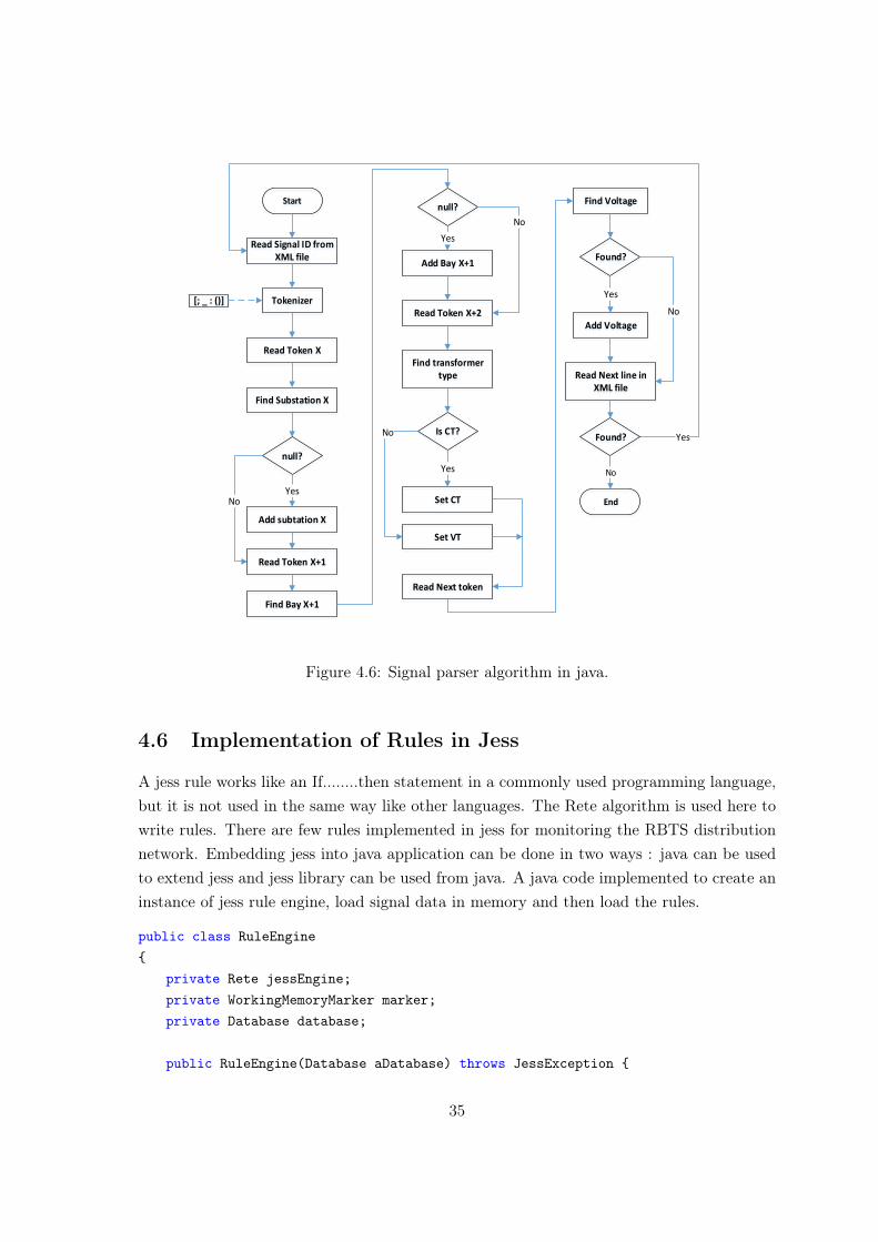
Read Signal ID from XML file
Start
Tokenizer[; _ : ()]
Read Token X
Find Substation X
null?
Add subtation X
YesNo
Read Token X+1
Find Bay X+1
null?
Add Bay X+1
Yes
Read Token X+2
No
Find transformer type
Is CT?
Set CT
Yes
Set VT
No
Read Next token
Found?
Find Voltage
Add Voltage
Yes
Read Next line in XML file
No
YesFound?
End
No
Figure 4.6: Signal parser algorithm in java.
4.6 Implementation of Rules in Jess
A jess rule works like an If........then statement in a commonly used programming language,but it is not used in the same way like other languages. The Rete algorithm is used here towrite rules. There are few rules implemented in jess for monitoring the RBTS distributionnetwork. Embedding jess into java application can be done in two ways : java can be usedto extend jess and jess library can be used from java. A java code implemented to create aninstance of jess rule engine, load signal data in memory and then load the rules.
public class RuleEngine{
private Rete jessEngine;private WorkingMemoryMarker marker;private Database database;
public RuleEngine(Database aDatabase) throws JessException {
35

// Create a Jess rule enginejessEngine = new Rete();jessEngine.reset();// Load the Jess rulesjessEngine.batch("RulesRepository.clp");// Load the signal data into working memorydatabase = aDatabase;
// Mark end of signal data for latermarker = jessEngine.mark();
}}
To work with jess in a java application at first it is needed to create a jess.Rete class,which itself a rule engine contains its own working memory, rules, agenda etc. The Database
interface is created in jess which will load all the signal tags along with their measured realtime value in working memory. It is an application specific data access wrapper. To processan ordered signal the jess engine has to follow four steps,
• Reset the engine for getting back to initial state.
• Load ordered signal data to working memory.
• Fire the appropriate rules.
• Get the result.
The rules will be used here to check the voltage fluctuation and to calculate the contri-bution of DG in the network. The file contains rules have to save as .clp file, for exampleRulesRepository.clp. Related java class has to import into .clp file for working with all thevariable mentioned there . It can be done by using deftemplate function.
(deftemplate VoltageSignal (declare (from-class VoltageSignal)))(deftemplate CurrentSignal (declare (from-class CurrentSignal)))(deftemplate DERSignal (declare (from-class DERSignal)))
After importing the java class to jess rules can be developed by using the variables de-clared in java class. In this thesis work three rules has been implemented for finding outany anomaly in the line voltage.defrule funtion is used to write rule in jess.
Rule 1: This rule is implemented for checking if the measured voltage value is withinthe acceptable range or not. Here VoltageSignal is a java class imported into jess by deftemplate
function. measuredValue and thresholdValue are two variables declared in java. measuredValue
contains all the real time measurements of voltage form RT-Lab.OPC server and thresholdValue
contains threshold values.
36

(defrule Generate-an-alarm-for-acceptable"If measured value is not greater than nominal value"?y <- (VoltageSignal {measuredValue <= thresholdValue})=>
(printout t "Acceptable measured Value" crlf ))
Rule 2: This rule can be explained in the same way as rule 1. It is designed for checkingif there is any high voltage rise in distribution network.
(defrule Generate-an-alarm-for-overload"If measured value is greater than nominal value"?x <- (VoltageSignal {measuredValue > thresholdValue})=>(printout t "Line Overloaded" crlf))
Rule 3: Actual contribution of each distributed generation unit in the network can becalculated in the following way.
(defrule generation_of_each_DG(CurrentSignal (cTNumber ?x)(measuredCurrent ?y)(cPhase ?z))(DERSignal (vTNumber ?e) (measuredVoltage ?f) (vPhase ?g) )(and (CurrentSignal {cTNumber == ?e} )
(DERSignal {vPhase == ?z}) )=>(printout t "Total Generation : " (* ?y ?f) crlf))
4.7 JADE Ontology Development
In this project an ontology has been developed in JADE based on IEC 61175 signal structureto organize information transferred between agents [22]. In communication system ontologyprovides a way to structure the information for agents to get a clear understanding of thesemantics of knowledge and agree on the terminologies. Depending on the expressivenessof an ontology different kind of components can be defined. There basic components areconcept, predicates and agent action. The structure of this ontology called IEC 61175ontology is shown in figure 4.7.
37

IEC 61175 ontology
Concepts
Predicates
AgentAction
DERSignal(meaValue, nomValue, vtPhase, vtNumber)
CurrentSignal(meaValue, ctPhase, ctNumber)
VoltageSignal(meaValue, nomValue, vtPhase, vtNumber)
isVoltageAcceptable
isVoltageBeyondThreshold
isSignalDER
generateAlarm
calculateTotalGeneration
Figure 4.7: Structure of IEC 61175 Ontology
Concepts are basically sets of expression that indicates entities with a complex slotstructure. Predicates are expressions that say about the some status in the system that canbe either true or false. The term agent action defines some special concepts that refer toactions that can be performed by the agents.
38
5Signals Mapping and Tree View
In this chapter it will be discussed the interfacing with server, signals mapping in the OPCserver, structure of python based OpalApi and the structure of GUI that has been im-plemented for this thesis work. Some details of Jade ontology will also discussed in thissection.
5.1 Interfacing with RT-Lab.OPC Server
RT-Lab.OPC server is the OPC gateway to RT-Lab simulator that accommodates commonautomation device and supervision tools with RT-Lab. It can handles huge number of sim-ulation signal and also allows real time access to any signal.
Real time signals or parameters from the distribution network implemented in RT-Labcan be mapped to RT-Lab.OPC server by an XML file. For mapping and fetching signalsfirst the network need to be loaded and executed in RT-Lab. When the model is running inOPAl-RT than select the run tab in the OPC pop up window. Then import the XML file tothe mapping file tab of RT-Lab.OPC server shown in figure 5.1. After importing the modeland xml file select the dynamic acquisition tab and the set the value one by one. Finally allthis configuration needs to save before run the RT-Lab.OPC server. RT-Lab version 10.5.9is used to follow the procedure described above. It may not be applicable for RT-Lab version10.7.
Later on for fetching signals to the server a python based Api has implemented forworking with RT-Lab version 10.7.
39
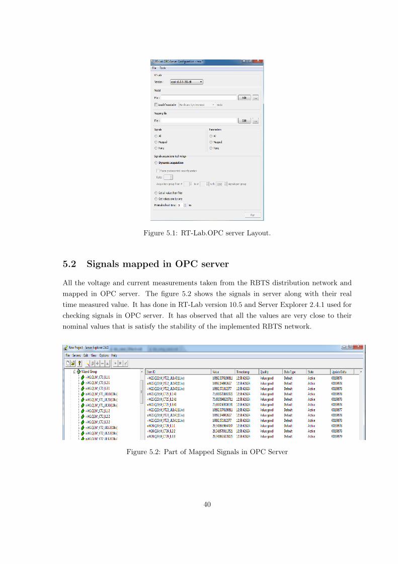
Figure 5.1: RT-Lab.OPC server Layout.
5.2 Signals mapped in OPC server
All the voltage and current measurements taken from the RBTS distribution network andmapped in OPC server. The figure 5.2 shows the signals in server along with their realtime measured value. It has done in RT-Lab version 10.5 and Server Explorer 2.4.1 used forchecking signals in OPC server. It has observed that all the values are very close to theirnominal values that is satisfy the stability of the implemented RBTS network.
Figure 5.2: Part of Mapped Signals in OPC Server
40
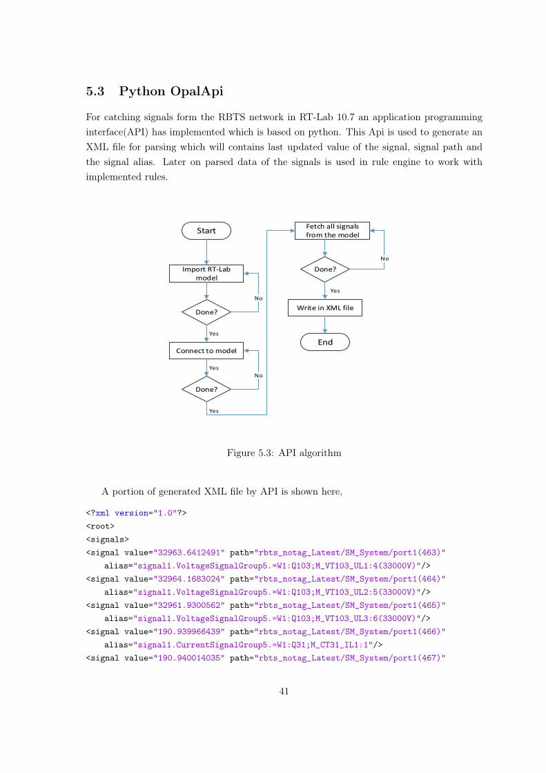
5.3 Python OpalApi
For catching signals form the RBTS network in RT-Lab 10.7 an application programminginterface(API) has implemented which is based on python. This Api is used to generate anXML file for parsing which will contains last updated value of the signal, signal path andthe signal alias. Later on parsed data of the signals is used in rule engine to work withimplemented rules.
Import RT-Lab model
Start
Done?
Connect to model
Yes
No
Fetch all signals from the model
Done?
Yes
No
Yes
Done?
Write in XML file
Yes
No
End
Figure 5.3: API algorithm
A portion of generated XML file by API is shown here,
<?xml version="1.0"?><root><signals><signal value="32963.6412491" path="rbts_notag_Latest/SM_System/port1(463)"
alias="signal1.VoltageSignalGroup5.=W1:Q103;M_VT103_UL1:4(33000V)"/><signal value="32964.1683024" path="rbts_notag_Latest/SM_System/port1(464)"
alias="signal1.VoltageSignalGroup5.=W1:Q103;M_VT103_UL2:5(33000V)"/><signal value="32961.9300562" path="rbts_notag_Latest/SM_System/port1(465)"
alias="signal1.VoltageSignalGroup5.=W1:Q103;M_VT103_UL3:6(33000V)"/><signal value="190.939966439" path="rbts_notag_Latest/SM_System/port1(466)"
alias="signal1.CurrentSignalGroup5.=W1:Q31;M_CT31_IL1:1"/><signal value="190.940014035" path="rbts_notag_Latest/SM_System/port1(467)"
41
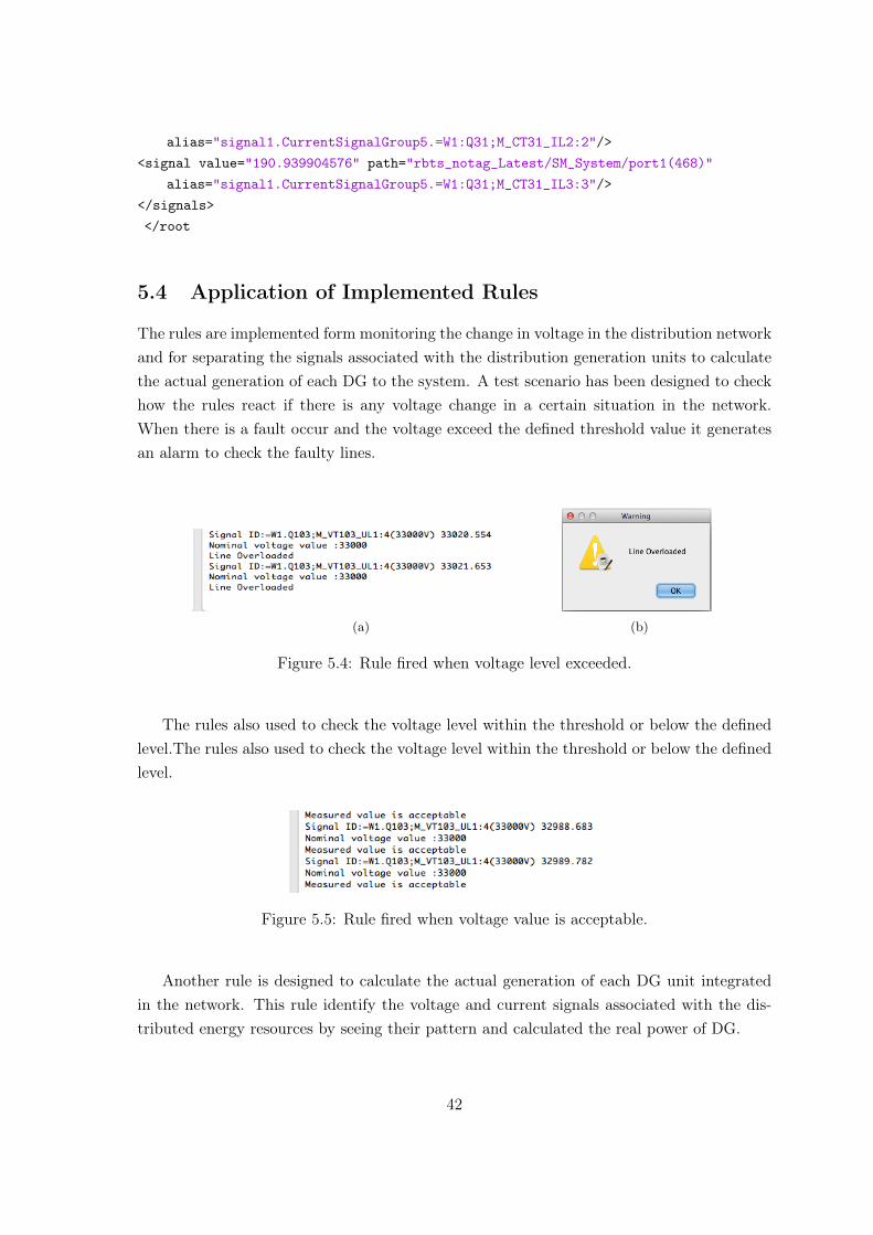
alias="signal1.CurrentSignalGroup5.=W1:Q31;M_CT31_IL2:2"/><signal value="190.939904576" path="rbts_notag_Latest/SM_System/port1(468)"
alias="signal1.CurrentSignalGroup5.=W1:Q31;M_CT31_IL3:3"/></signals></root
5.4 Application of Implemented Rules
The rules are implemented form monitoring the change in voltage in the distribution networkand for separating the signals associated with the distribution generation units to calculatethe actual generation of each DG to the system. A test scenario has been designed to checkhow the rules react if there is any voltage change in a certain situation in the network.When there is a fault occur and the voltage exceed the defined threshold value it generatesan alarm to check the faulty lines.
(a) (b)
Figure 5.4: Rule fired when voltage level exceeded.
The rules also used to check the voltage level within the threshold or below the definedlevel.The rules also used to check the voltage level within the threshold or below the definedlevel.
Figure 5.5: Rule fired when voltage value is acceptable.
Another rule is designed to calculate the actual generation of each DG unit integratedin the network. This rule identify the voltage and current signals associated with the dis-tributed energy resources by seeing their pattern and calculated the real power of DG.
42
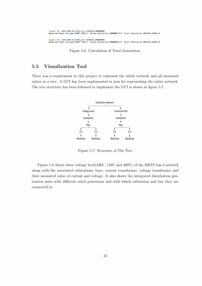
Figure 5.6: Calculation of Total Generation.
5.5 Visualization Tool
There was a requirement in this project to represent the whole network and all measuredvalues in a tree. A GUI has been implemented in java for representing the entire network.The tree structure has been followed to implement the GUI is shown in figure 5.7.
Distribution Network
Voltage levels Connected DGs
Substations
Bays
CTs VTs
MeaValue MeaValue
Substations
Bays
CTs VTs
MeaValueMeaValue
Figure 5.7: Structure of The Tree
Figure 5.8 shows three voltage level(33kV, 11kV and 400V) of the RBTS bus-4 networkalong with the associated substations, bays, current transformer, voltage transformer andtheir measured value of current and voltage. It also shows the integrated distribution gen-eration units with different rated generation and with which substation and bay they areconnected to.
43

Figure 5.8: Structure of The GUI
This structure is a graphical representation of signals along with their measured value.The section marked on figure 5.8 shows two signals which are belong to 400 V. One is voltagesignal which has a measured value 391.06953118 V and another one is current measurementof 804.61301 Amps. Both signals are valid in =W302.Q302 domain. The measurements aretaken from voltage transformer VT302 and the current transformer CT302.
Nominal Value of VoltageSubstation ID
Bay ID
Voltage Transformer ID
Measured Voltage
Current Transformer IDMeasured Current
Figure 5.9: Node Explanation
44

6Conclusion and Future works
6.1 Conclusion
Semantic interpretation (SI) of signals is the way of mapping syntactically designated sig-nals to a representation of its meaning. Semantic expressiveness of signals is required at enduser interface to deal with large amount of data involved in the communication system of anetwork [21]. SI allows multiple utterance to return same result.An IEEE Bus 4 referenceelectrical distribution network in Simulink platform had used in this master thesis projectto perform modelling of signals. The signal designation standard IEC 61175 used in thisproject to name the signals in internationally recognised way. This standard has exten-sive application in electrical system, in external communication, in the HMI, in controllingdevice with the internal numerical communication etc. Some other standard such as IEC60076-1, IEC 61850-7-4 and IEC 61346-2 were also studied for naming some components inthe network. Parse tree is the input to a semantic interpretor. For this tree generation it isneeded to generate an XML file of the all signals associated with the distribution networkalong with their measured value. Until mapping signals to the server all the works hadbeen on RT-Lab version 10.5 but later on the upgraded version 10.7 the entire process wasnot working. So to be done the analysis by thesis time frame an interface program hadimplemented on Python to fetch all signals and the output of this interface is an XML filewith the latest updated measured value of the signals. The XML file generated by the in-terface was containing more then 32000 signals so it challenging to pick up only the desiredsignals. A parser program had implemented on Java to pick up the mapped signals from theXML file and to create a database for the Jess rule engine. During this phase a GUI alsobeen implemented for representing the entire RBTS bus-4 in an organized way. During thisproject the most challenging task was integrating the Jess rule engine to the Java parserand make it work. Two approaches can be followed to do this integration, either calling Jessfunctions from Java or calling Java methods from Jess. Embedding Jess in Java applicationhad been followed to perform this thesis work. The rules were designed for monitoring the
45

changes in voltage and for calculating the actual generation of each distributed generationunits integrated into the reference network.
Form the present study it can be concluded that,
• detailed and consistent signal modeling with enable development of advanced protec-tion and control application which are crucial for realization of DG integration andSmart grid.
• Signal modeling can improve reliability of operation as well as end application.
• a visualization tool and rule based system can be helpful for advance monitoring andcontrol of the entire distribution network.
• Applying the IEC 61175 standard in any electrical network for signal designation canbe helpful to lessen the complexity of commissioning and configuring for distributioncompanies.
6.2 Future Recommendations
In future this network can be used as a prototype for working with semantic interpretation.Due to some limitations of RT-Lab that has been used during this project and the hugesize of the RBTS bus-4 network it was not possible deal with breakers and switches. Soa protection and communication system can be developed for this network by integratingmore devices. Technical documentation is another important issue for a real life substation.For documentation of signals in this reference network IEC 61082-1 can be followed.
46

References
[1] SMB Smart Grid Strategic Group (SG3),"IEC Smart Grid StandardizationRoadmap",June 2010; Edition 1.0.
[2] R. E. Mackiewicz, Member IEEE "Overview of IEC 61850 and Benefits" ,Power Engi-neering Society General Meeting, 2006 IEEE.
[3] N. Rugthaicharoencheep, T. Langtharthong "Reliability Improvement with OptimalPlacement of Distributed Generation in Distribution System"World Academy of Science,Engineering and Technology, International Journal of Electrical, Robotics, Electronicsand Communications Engineering Vol:7 No:10, 2013.
[4] E. Lakervi, E. J. Holmes "Electricity Distribution Network Design" , Institution of En-gineering and Technology; 2nd Revised edition edition, ISBN-13: 978-0863413087, page15-20.
[5] Lina Bertling, Senior Member, IEEE, Pramod Bangalore,Student Member, IEEE, LeAnh Tuan, Member, IEEE "On the use of reliability test systems:A literature survey"2011 IEEE Power and Energy Society General Meeting,July 2011, Detroit, Michigan,USA.
[6] R. Billinton, S. Kumar, N. Chowdhury, K. Chu, K. Debnath, L. Goel, E.Khan, P. Kos, G.Nourbaksh„ J. Oteng- Adjei, "A Reliability Test System For Educational Purposes-BasicData", IEEE Transactions on Power Systems, Vol. 4, No. 3, August 1989.
[7] ] R.N. Allan, R. Billinton, I. Sjarief, L. Goel, and K. S. So. A reliability test system foreducational purposes-basic distribution system data and results. Power Systems, IEEETransactions on, 6(2):813–820, 1991. ISSN 0885-8950. doi: 10.1109/59.76730.
47

[8] Kang Longyun, Zhang Yanning, Cao Binggang " Wind-Solar-Biogas Renewable EnergyDistributed Power system." Clean Electrical Power, 2009 International Conference. Pub-lisher: IEEE.
[9] M. Vaziri, Senior Member, IEEE, S. Vadhva, Member, IEEE, T. Oneal, M. Johnson"Smart Grid, Distributed Generation, and Standards." Proceedings of the IEEE PESGeneral Meeting-978-1-4577-1002-5/11 Summer 2011, July 24-28 2011. Detroit, Michi-gan, USA.
[10] J.A. Hollman, J.R. Marti, Real time network simulation with PCcluster. IEEE Trans.Power Syst. 18(2), 563-569 (2008)
[11] Suresh Mikkili, Anup Kumar Panda, Jayanthi Prattipati, "Review of Real-Time Simu-lator and the Steps Involved for of a Model from MATLAB/SIMULINK to Real-Time"21 May 2014 The Institution of Engineers (India).
[12] Ernest Friedman-Hill,"Jess in action, A rule-based system in java",by Manning Publi-cations Co 2003.
[13] IEC/TC or SC:3 " Industrial systems, installations and equipment and industrial prod-ucts - Designation of signals." IEC 61175/Ed.3, 2013.
[14] In-Su Bae and Jin-O Kim. Reliability evaluation of customers in a microgrid. Power Sys-tems, IEEE Transactions on, 23(3):14161422, Aug 2008. ISSN 0885-8950. doi: 10.1109/T-PWRS.2008.926710.
[15] IEC 61346, "Industrial systems, Installations and Equipment and Industrial Products-Structuring Principles and Reference Designations",IEC 61346-2:2000.
[16] International standard IEC 60076-1 Power Transformer, Edition 2.1, Reference numberIEC 60076-1: 1993+A1:1999(E).
[17] John A. DeDad, "The basics of transformer, Part 5", Electrical Construction and Main-tenance. www.ecmweb.com/content, visited: Sept 11, 2014.
[18] RT-LAB Version 10.2 User Guide, RTLAB-UG-102-00.
[19] ChenWei Yang, Valeriy Vyatkin, Nirmal-Kumar C Nair, Julien Chouinard, "Pro-grammable Logic for IEC 61850 Logical Nodes by means of IEC 61499",978-1-61284-972-0/11/, 2011 IEEE.
[20] Moselle, B. and Padilla, J. and Schmalensee, R. "Harnessing Renewable Energy inElectric Power Systems: Theory, Practice, Policy",isbn= 9781136522130, publisher=Taylor & Francis,2010.
48

[21] Graeme Hirst, "Simantic Interpretation and Ambiguity" , Department of ComputerScience, University of Toronto, Toronto, Canada M5S 1A4.
[22] Arshad Saleem, Student-Member, IEEE, Kai Heussen, Student-Member, IEEE, andMorten Lind,"Agent Services for Situation Aware Control of Power Systems With Dis-tributed Generation", IEEE PES GENERAL MEETING 2009.
[23] http : //www.ruggedcom.com/applications/electric − utilities/evolution/ visited on10 Oct 2014.
[24] J.A.P. Lopes, N. Hatziargyriou, J. Mutale, P. Djapic, N. Jenkins "Integrating dis-tributed generation into electric power systems: A review of drivers, challenges andopportunities", Electric Power Systems Research 77 (2007) 1189–1203.
49

AAppendix
MATPOWER Version 4.1, 14-Dec-2011 – AC Power Flow (Newton)Newton’s method power flow converged in 4 iterations.Converged in 0.08 seconds================================================================================|System Summary |================================================================================How many? How much? P (MW) Q (MVAr)——— —————- ————- ——————-Buses 68 Total Gen Capacity 100.0 -140.0 to 200.0Generators 1 On-line Capacity 100.0 -140.0 to 200.0Committed Gens 1 Generation (actual) 42.0 4.1Loads 38 Load 40.2 0.0Fixed 38 Fixed 40.2 0.0Dispatchable 0 Dispatchable -0.0 of -0.0 -0.0Shunts 0 Shunt (inj) -0.0 0.0Branches 67 Losses (Iˆ2 * Z) 1.80 4.06Transformers 0 Branch Charging (inj) - 0.0Inter-ties 0 Total Inter-tie Flow 0.0 0.0Areas 1Minimum Maximum————————- —————————————–Voltage Magnitude 0.923 p.u. @ bus 13 1.000 p.u. @ bus 1Voltage Angle -8.87 deg @ bus 13 0.00 deg @ bus 1P Losses (Iˆ2*R) - 0.15 MW @ line 1-33Q Losses (Iˆ2*X) - 0.35 MVAr @ line 1-33================================================================================|Bus Data |
50

================================================================================Bus Voltage Generation Load# Mag(pu) Ang(deg) P (MW) Q (MVAr) P (MW) Q (MVAr)——– ———— ———— ————- ————- ———— ————-1 1.000 0.000* 42.02 4.06 - -2 0.977 -2.344 - - - -3 0.975 -2.632 - - 0.89 0.004 0.957 -4.566 - - - -5 0.954 -4.941 - - 0.89 0.006 0.941 -6.465 - - - -7 0.939 -6.776 - - 0.89 0.008 0.930 -7.905 - - - -9 0.927 -8.330 - - 0.89 0.0010 0.927 -8.270 - - 0.81 0.0011 0.926 -8.465 - - - -12 0.923 -8.789 - - 0.67 0.0013 0.923 -8.867 - - 0.89 0.0014 0.974 -2.935 - - 1.63 0.0015 0.978 -2.406 - - - -16 0.964 -4.189 - - - -17 0.956 -5.216 - - 2.44 0.0018 0.959 -4.734 - - - -19 0.954 -5.469 - - 1.63 0.0020 0.976 -2.607 - - 0.89 0.0021 0.979 -2.225 - - - -22 0.966 -3.777 - - - -23 0.963 -4.146 - - 0.89 0.0024 0.952 -5.508 - - - -25 0.949 -5.888 - - 0.89 0.0026 0.950 -5.787 - - 0.81 0.0027 0.944 -6.499 - - - -28 0.941 -6.853 - - 0.81 0.0029 0.941 -6.966 - - - -30 0.939 -7.202 - - 0.67 0.0031 0.938 -7.261 - - 0.67 0.0032 0.970 -3.127 - - 0.89 0.0033 0.973 -2.764 - - - -34 0.951 -5.273 - - - -35 0.949 -5.577 - - 0.89 0.00
51

36 0.949 -5.653 - - 0.89 0.0037 0.937 -7.058 - - - -38 0.934 -7.450 - - 0.89 0.0039 0.935 -7.345 - - 0.81 0.0040 0.929 -8.079 - - - -41 0.927 -8.445 - - 0.81 0.0042 0.926 -8.562 - - - -43 0.924 -8.866 - - 0.67 0.0044 0.924 -8.805 - - 0.67 0.0045 0.977 -2.711 - - 1.63 0.0046 0.982 -2.054 - - - -47 0.974 -3.109 - - - -48 0.968 -3.822 - - 1.63 0.0049 0.968 -3.777 - - - -50 0.964 -4.317 - - 1.63 0.0051 0.976 -2.780 - - 1.63 0.0052 0.980 -2.253 - - - -53 0.965 -4.031 - - - -54 0.960 -4.712 - - 1.63 0.0055 0.956 -5.125 - - - -56 0.950 -5.958 - - 2.44 0.0057 0.975 -2.696 - - 0.89 0.0058 0.978 -2.312 - - - -59 0.964 -3.939 - - - -60 0.961 -4.334 - - 0.89 0.0061 0.950 -5.659 - - - -62 0.948 -5.964 - - 0.89 0.0063 0.947 -6.066 - - 0.89 0.0064 0.942 -6.652 - - - -65 0.940 -6.937 - - 0.81 0.0066 0.937 -7.303 - - - -67 0.935 -7.686 - - 0.81 0.0068 0.936 -7.539 - - 0.67 0.00——– ——– ——– ——–Total: 42.02 4.06 40.21 0.00================================================================================|Branch Data |================================================================================Brnch From To From Bus Injection To Bus Injection Loss (Iˆ2 * Z)
52
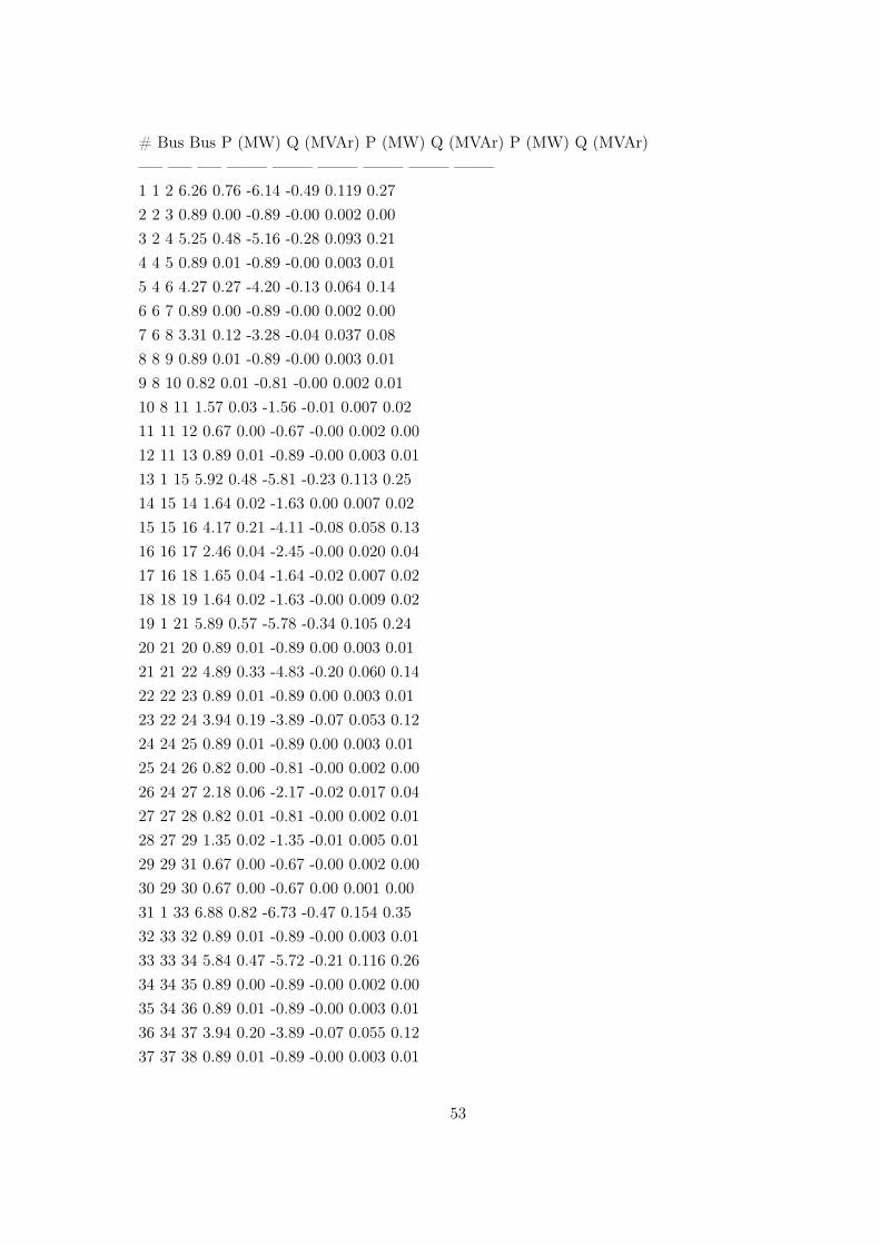
# Bus Bus P (MW) Q (MVAr) P (MW) Q (MVAr) P (MW) Q (MVAr)—– —– —– ——– ——– ——– ——– ——– ——–1 1 2 6.26 0.76 -6.14 -0.49 0.119 0.272 2 3 0.89 0.00 -0.89 -0.00 0.002 0.003 2 4 5.25 0.48 -5.16 -0.28 0.093 0.214 4 5 0.89 0.01 -0.89 -0.00 0.003 0.015 4 6 4.27 0.27 -4.20 -0.13 0.064 0.146 6 7 0.89 0.00 -0.89 -0.00 0.002 0.007 6 8 3.31 0.12 -3.28 -0.04 0.037 0.088 8 9 0.89 0.01 -0.89 -0.00 0.003 0.019 8 10 0.82 0.01 -0.81 -0.00 0.002 0.0110 8 11 1.57 0.03 -1.56 -0.01 0.007 0.0211 11 12 0.67 0.00 -0.67 -0.00 0.002 0.0012 11 13 0.89 0.01 -0.89 -0.00 0.003 0.0113 1 15 5.92 0.48 -5.81 -0.23 0.113 0.2514 15 14 1.64 0.02 -1.63 0.00 0.007 0.0215 15 16 4.17 0.21 -4.11 -0.08 0.058 0.1316 16 17 2.46 0.04 -2.45 -0.00 0.020 0.0417 16 18 1.65 0.04 -1.64 -0.02 0.007 0.0218 18 19 1.64 0.02 -1.63 -0.00 0.009 0.0219 1 21 5.89 0.57 -5.78 -0.34 0.105 0.2420 21 20 0.89 0.01 -0.89 0.00 0.003 0.0121 21 22 4.89 0.33 -4.83 -0.20 0.060 0.1422 22 23 0.89 0.01 -0.89 0.00 0.003 0.0123 22 24 3.94 0.19 -3.89 -0.07 0.053 0.1224 24 25 0.89 0.01 -0.89 0.00 0.003 0.0125 24 26 0.82 0.00 -0.81 -0.00 0.002 0.0026 24 27 2.18 0.06 -2.17 -0.02 0.017 0.0427 27 28 0.82 0.01 -0.81 -0.00 0.002 0.0128 27 29 1.35 0.02 -1.35 -0.01 0.005 0.0129 29 31 0.67 0.00 -0.67 -0.00 0.002 0.0030 29 30 0.67 0.00 -0.67 0.00 0.001 0.0031 1 33 6.88 0.82 -6.73 -0.47 0.154 0.3532 33 32 0.89 0.01 -0.89 -0.00 0.003 0.0133 33 34 5.84 0.47 -5.72 -0.21 0.116 0.2634 34 35 0.89 0.00 -0.89 -0.00 0.002 0.0035 34 36 0.89 0.01 -0.89 -0.00 0.003 0.0136 34 37 3.94 0.20 -3.89 -0.07 0.055 0.1237 37 38 0.89 0.01 -0.89 -0.00 0.003 0.01
53
38 37 39 0.82 0.00 -0.81 -0.00 0.002 0.0039 37 40 2.18 0.06 -2.17 -0.02 0.017 0.0440 40 41 0.82 0.01 -0.81 -0.00 0.002 0.0141 40 42 1.35 0.02 -1.35 -0.01 0.005 0.0142 42 43 0.67 0.00 -0.67 -0.00 0.002 0.0043 42 44 0.67 0.00 -0.67 -0.00 0.001 0.0044 1 46 5.03 0.32 -4.95 -0.14 0.081 0.1845 46 45 1.64 0.02 -1.63 0.00 0.008 0.0246 46 47 3.31 0.12 -3.28 -0.06 0.027 0.0647 47 48 1.64 0.02 -1.63 0.00 0.009 0.0248 47 49 1.65 0.03 -1.64 -0.02 0.009 0.0249 49 50 1.64 0.02 -1.63 -0.00 0.007 0.0250 1 52 5.92 0.49 -5.82 -0.25 0.106 0.2451 52 51 1.64 0.02 -1.63 0.00 0.007 0.0252 52 53 4.18 0.23 -4.12 -0.10 0.058 0.1353 53 54 1.64 0.02 -1.63 -0.00 0.009 0.0254 53 55 2.48 0.08 -2.46 -0.04 0.021 0.0555 55 56 2.46 0.04 -2.44 -0.00 0.016 0.0456 1 58 6.12 0.62 -6.01 -0.37 0.114 0.2657 58 57 0.89 0.01 -0.89 0.00 0.003 0.0158 58 59 5.12 0.36 -5.05 -0.21 0.066 0.1559 59 60 0.89 0.01 -0.89 0.00 0.003 0.0160 59 61 4.16 0.21 -4.11 -0.08 0.056 0.1361 61 62 0.89 0.00 -0.89 0.00 0.002 0.0062 61 63 0.89 0.01 -0.89 0.00 0.003 0.0163 61 64 2.33 0.07 -2.31 -0.03 0.018 0.0464 64 65 0.82 0.00 -0.81 -0.00 0.002 0.0065 64 66 1.50 0.03 -1.49 -0.01 0.008 0.0266 66 67 0.82 0.01 -0.81 -0.00 0.002 0.0167 66 68 0.67 0.00 -0.67 -0.00 0.001 0.00——– ——–Total: 1.805 4.06
54

BAppendix
XML file of Mapped Signals
<?xml version="1.0"?>
<root>
<signals>
<signal path="rbts_notag_Latest/SM_System/SS3/CT101/Sqrt/port1(1)"alias="=W1.Q101;M_CT101_IL1:10"/>
<signal path="rbts_notag_Latest/SM_System/SS3/CT101/Sqrt/port1(2)"alias="=W1.Q101;M_CT101_IL2:11"/>
<signal path="rbts_notag_Latest/SM_System/SS3/CT101/Sqrt/port1(3)"alias="=W1.Q101;M_CT101_IL3:12"/>
<signal path="rbts_notag_Latest/SM_System/SS3/VT101/Sqrt/port1(1)"alias="=W1.Q101;M_VT101_UL1:10(33000V)"/>
<signal path="rbts_notag_Latest/SM_System/SS3/VT101/Sqrt/port1(2)"alias="=W1.Q101;M_VT101_UL2:11(33000V)"/>
<signal path="rbts_notag_Latest/SM_System/SS3/VT101/Sqrt/port1(3)"alias="=W1.Q101;M_VT101_UL3:12(33000V)"/>
<signal path="rbts_notag_Latest/SM_System/SS3/CT103/Sqrt/port1(1)"alias="=W1.Q103;M_CT103_IL1:4"/>
<signal path="rbts_notag_Latest/SM_System/SS3/CT103/Sqrt/port1(2)"alias="=W1.Q103;M_CT103_IL2:5"/>
<signal path="rbts_notag_Latest/SM_System/SS3/CT103/Sqrt/port1(3)"alias="=W1.Q103;M_CT103_IL3:6"/>
<signal path="rbts_notag_Latest/SM_System/SS3/VT103/Sqrt/port1(1)"alias="=W1.Q103;M_VT103_UL1:4(33000V)"/>
55

<signal path="rbts_notag_Latest/SM_System/SS3/VT103/Sqrt/port1(2)"alias="=W1.Q103;M_VT103_UL2:5(33000V)"/>
<signal path="rbts_notag_Latest/SM_System/SS3/VT103/Sqrt/port1(3)"alias="=W1.Q103;M_VT103_UL3:6(33000V)"/>
<signal path="rbts_notag_Latest/SM_System/SS1/CT100/Sqrt/port1(1)"alias="=W1.Q100;M_CT100_IL1:1"/>
<signal path="rbts_notag_Latest/SM_System/SS1/CT100/Sqrt/port1(2)"alias="=W1.Q100;M_CT100_IL2:2"/>
<signal path="rbts_notag_Latest/SM_System/SS1/CT100/Sqrt/port1(3)"alias="=W1.Q100;M_CT100_IL3:3"/>
<signal path="rbts_notag_Latest/SM_System/SS1/VT100/Sqrt/port1(1)"alias="=W1.Q100;M_VT100_UL1:1(33000V)"/>
<signal path="rbts_notag_Latest/SM_System/SS1/VT100/Sqrt/port1(2)"alias="=W1.Q100;M_VT100_UL2:2(33000V)"/>
<signal path="rbts_notag_Latest/SM_System/SS1/VT100/Sqrt/port1(3)"alias="=W1.Q100;M_VT100_UL3:3(33000V)"/>
<signal path="rbts_notag_Latest/SM_System/SS5/CT102/Sqrt/port1(1)"alias="=W1.Q102;M_CT102_IL1:4"/>
<signal path="rbts_notag_Latest/SM_System/SS5/CT102/Sqrt/port1(2)"alias="=W1.Q102;M_CT102_IL2:5"/>
<signal path="rbts_notag_Latest/SM_System/SS5/CT102/Sqrt/port1(3)"alias="=W1.Q102;M_CT102_IL3:6"/>
<signal path="rbts_notag_Latest/SM_System/SS5/VT102/Sqrt/port1(1)"alias="=W1.Q102;M_VT102_UL1:4(33000V)"/>
<signal path="rbts_notag_Latest/SM_System/SS5/VT102/Sqrt/port1(2)"alias="=W1.Q102;M_VT102_UL2:5(33000V)"/>
<signal path="rbts_notag_Latest/SM_System/SS5/VT102/Sqrt/port1(3)"alias="=W1.Q102;M_VT102_UL3:6(33000V)"/>
<signal path="rbts_notag_Latest/SM_System/SS2/CT1/Sqrt/port1(1)"alias="=W1.Q1;M_CT1_IL1:7"/>
<signal path="rbts_notag_Latest/SM_System/SS2/CT1/Sqrt/port1(2)"alias="=W1.Q1;M_CT1_IL2:8"/>
<signal path="rbts_notag_Latest/SM_System/SS2/CT1/Sqrt/port1(3)"alias="=W1.Q1;M_CT1_IL3:9"/>
<signal path="rbts_notag_Latest/SM_System/SS2/VT1/Sqrt/port1(1)"alias="=W1.Q1;M_VT1_UL1:7(11000V)"/>
<signal path="rbts_notag_Latest/SM_System/SS2/VT1/Sqrt/port1(2)"alias="=W1.Q1;M_VT1_UL2:8(11000V)"/>
<signal path="rbts_notag_Latest/SM_System/SS2/VT1/Sqrt/port1(3)"alias="=W1.Q1;M_VT1_UL3:9(11000V)"/>
<signal path="rbts_notag_Latest/SM_System/=W2;/CT2/Sqrt/port1(1)"alias="=W2.Q2;M_CT2_IL1:4"/>
<signal path="rbts_notag_Latest/SM_System/=W2;/CT2/Sqrt/port1(2)"alias="=W2.Q2;M_CT2_IL2:5"/>
56
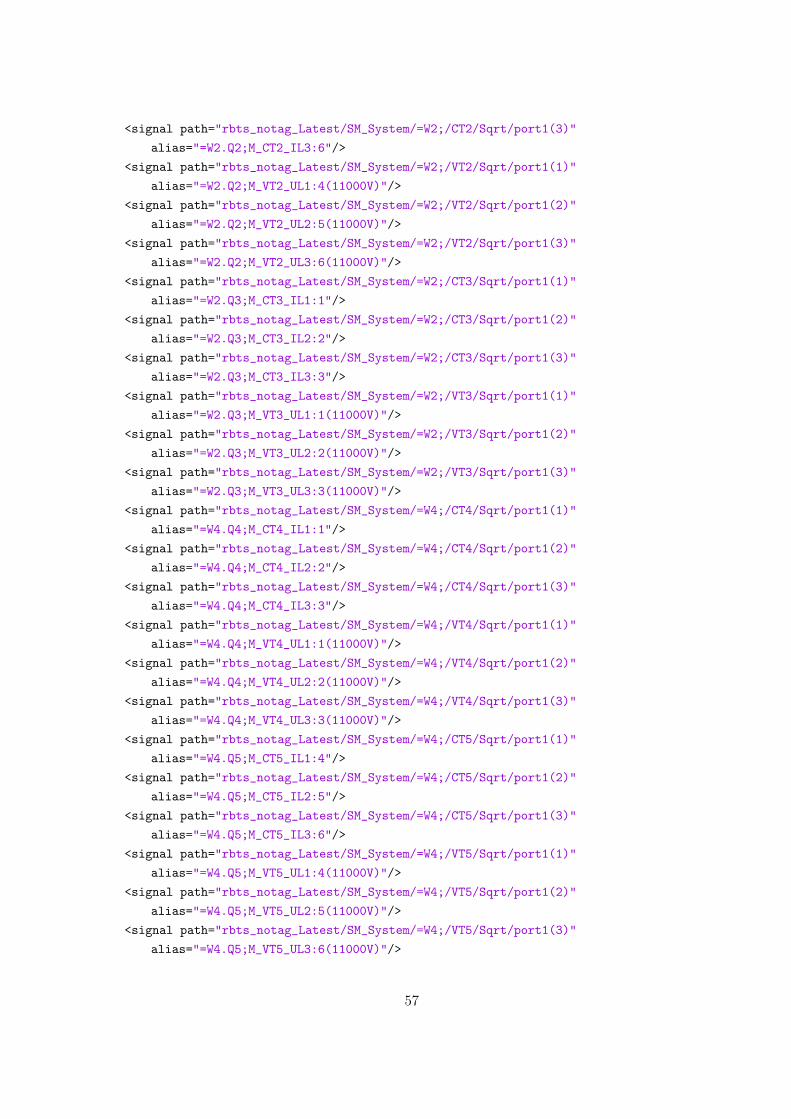
<signal path="rbts_notag_Latest/SM_System/=W2;/CT2/Sqrt/port1(3)"alias="=W2.Q2;M_CT2_IL3:6"/>
<signal path="rbts_notag_Latest/SM_System/=W2;/VT2/Sqrt/port1(1)"alias="=W2.Q2;M_VT2_UL1:4(11000V)"/>
<signal path="rbts_notag_Latest/SM_System/=W2;/VT2/Sqrt/port1(2)"alias="=W2.Q2;M_VT2_UL2:5(11000V)"/>
<signal path="rbts_notag_Latest/SM_System/=W2;/VT2/Sqrt/port1(3)"alias="=W2.Q2;M_VT2_UL3:6(11000V)"/>
<signal path="rbts_notag_Latest/SM_System/=W2;/CT3/Sqrt/port1(1)"alias="=W2.Q3;M_CT3_IL1:1"/>
<signal path="rbts_notag_Latest/SM_System/=W2;/CT3/Sqrt/port1(2)"alias="=W2.Q3;M_CT3_IL2:2"/>
<signal path="rbts_notag_Latest/SM_System/=W2;/CT3/Sqrt/port1(3)"alias="=W2.Q3;M_CT3_IL3:3"/>
<signal path="rbts_notag_Latest/SM_System/=W2;/VT3/Sqrt/port1(1)"alias="=W2.Q3;M_VT3_UL1:1(11000V)"/>
<signal path="rbts_notag_Latest/SM_System/=W2;/VT3/Sqrt/port1(2)"alias="=W2.Q3;M_VT3_UL2:2(11000V)"/>
<signal path="rbts_notag_Latest/SM_System/=W2;/VT3/Sqrt/port1(3)"alias="=W2.Q3;M_VT3_UL3:3(11000V)"/>
<signal path="rbts_notag_Latest/SM_System/=W4;/CT4/Sqrt/port1(1)"alias="=W4.Q4;M_CT4_IL1:1"/>
<signal path="rbts_notag_Latest/SM_System/=W4;/CT4/Sqrt/port1(2)"alias="=W4.Q4;M_CT4_IL2:2"/>
<signal path="rbts_notag_Latest/SM_System/=W4;/CT4/Sqrt/port1(3)"alias="=W4.Q4;M_CT4_IL3:3"/>
<signal path="rbts_notag_Latest/SM_System/=W4;/VT4/Sqrt/port1(1)"alias="=W4.Q4;M_VT4_UL1:1(11000V)"/>
<signal path="rbts_notag_Latest/SM_System/=W4;/VT4/Sqrt/port1(2)"alias="=W4.Q4;M_VT4_UL2:2(11000V)"/>
<signal path="rbts_notag_Latest/SM_System/=W4;/VT4/Sqrt/port1(3)"alias="=W4.Q4;M_VT4_UL3:3(11000V)"/>
<signal path="rbts_notag_Latest/SM_System/=W4;/CT5/Sqrt/port1(1)"alias="=W4.Q5;M_CT5_IL1:4"/>
<signal path="rbts_notag_Latest/SM_System/=W4;/CT5/Sqrt/port1(2)"alias="=W4.Q5;M_CT5_IL2:5"/>
<signal path="rbts_notag_Latest/SM_System/=W4;/CT5/Sqrt/port1(3)"alias="=W4.Q5;M_CT5_IL3:6"/>
<signal path="rbts_notag_Latest/SM_System/=W4;/VT5/Sqrt/port1(1)"alias="=W4.Q5;M_VT5_UL1:4(11000V)"/>
<signal path="rbts_notag_Latest/SM_System/=W4;/VT5/Sqrt/port1(2)"alias="=W4.Q5;M_VT5_UL2:5(11000V)"/>
<signal path="rbts_notag_Latest/SM_System/=W4;/VT5/Sqrt/port1(3)"alias="=W4.Q5;M_VT5_UL3:6(11000V)"/>
57

<signal path="rbts_notag_Latest/SM_System/=W6;/CT6/Sqrt/port1(1)"alias="=W6.Q6;M_CT6_IL1:1"/>
<signal path="rbts_notag_Latest/SM_System/=W6;/CT6/Sqrt/port1(2)"alias="=W6.Q6;M_CT6_IL2:2"/>
<signal path="rbts_notag_Latest/SM_System/=W6;/CT6/Sqrt/port1(3)"alias="=W6.Q6;M_CT6_IL3:3"/>
<signal path="rbts_notag_Latest/SM_System/=W6;/VT6/Sqrt/port1(1)"alias="=W6.Q6;M_VT6_UL1:1(11000V)"/>
<signal path="rbts_notag_Latest/SM_System/=W6;/VT6/Sqrt/port1(2)"alias="=W6.Q6;M_VT6_UL2:2(11000V)"/><signal path="rbts_notag_Latest/SM_System/=W6;/VT6/Sqrt/port1(3)"
alias="=W6.Q6;M_VT6_UL3:3(11000V)"/><signal path="rbts_notag_Latest/SM_System/=W6;/CT7/Sqrt/port1(1)"
alias="=W6.Q7;M_CT7_IL1:7"/><signal path="rbts_notag_Latest/SM_System/=W6;/CT7/Sqrt/port1(2)"
alias="=W6.Q7;M_CT7_IL2:8"/><signal path="rbts_notag_Latest/SM_System/=W6;/CT7/Sqrt/port1(3)"
alias="=W6.Q7;M_CT7_IL3:9"/><signal path="rbts_notag_Latest/SM_System/=W6;/VT7/Sqrt/port1(1)"
alias="=W6.Q7;M_VT7_UL1:7(11000V)"/><signal path="rbts_notag_Latest/SM_System/=W6;/VT7/Sqrt/port1(2)"
alias="=W6.Q7;M_VT7_UL2:8(11000V)"/><signal path="rbts_notag_Latest/SM_System/=W6;/VT7/Sqrt/port1(3)"
alias="=W6.Q7;M_VT7_UL3:9(11000V)"/><signal path="rbts_notag_Latest/SM_System/=W8;/CT8/Sqrt/port1(1)"
alias="=W8.Q8;M_CT8_IL1:1"/><signal path="rbts_notag_Latest/SM_System/=W8;/CT8/Sqrt/port1(2)"
alias="=W8.Q8;M_CT8_IL2:2"/><signal path="rbts_notag_Latest/SM_System/=W8;/CT8/Sqrt/port1(3)"
alias="=W8.Q8;M_CT8_IL3:3"/><signal path="rbts_notag_Latest/SM_System/=W8;/VT8/Sqrt/port1(1)"
alias="=W8.Q8;M_VT8_UL1:1(11000V)"/><signal path="rbts_notag_Latest/SM_System/=W8;/VT8/Sqrt/port1(2)"
alias="=W8.Q8;M_VT8_UL2:2(11000V)"/><signal path="rbts_notag_Latest/SM_System/=W8;/VT8/Sqrt/port1(3)"
alias="=W8.Q8;M_VT8_UL3:3(11000V)"/><signal path="rbts_notag_Latest/SM_System/=W8;/CT9/Sqrt/port1(1)"
alias="=W8.Q9;M_CT9_IL1:4"/><signal path="rbts_notag_Latest/SM_System/=W8;/CT9/Sqrt/port1(2)"
alias="=W8.Q9;M_CT9_IL2:5"/><signal path="rbts_notag_Latest/SM_System/=W8;/CT9/Sqrt/port1(3)"
alias="=W8.Q9;M_CT9_IL3:6"/>
58
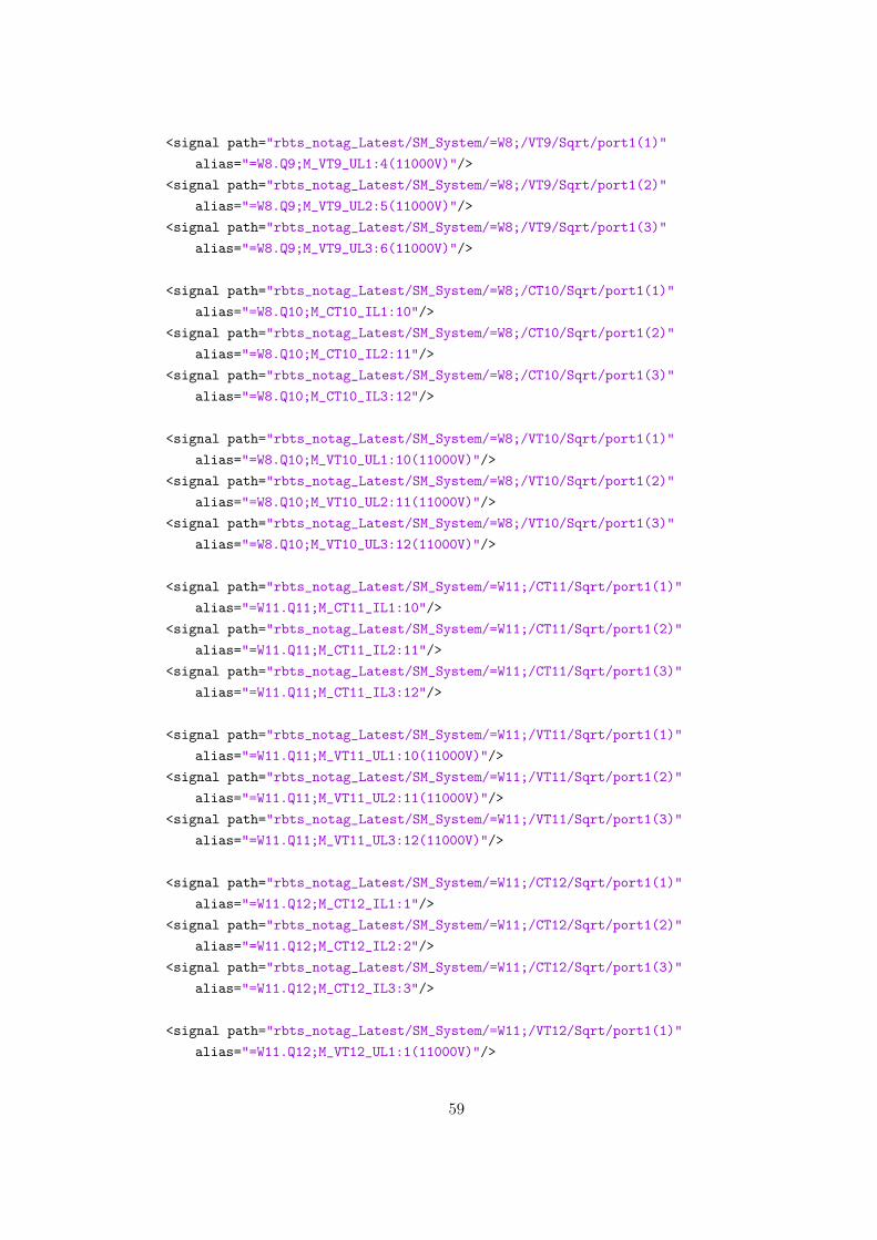
<signal path="rbts_notag_Latest/SM_System/=W8;/VT9/Sqrt/port1(1)"alias="=W8.Q9;M_VT9_UL1:4(11000V)"/>
<signal path="rbts_notag_Latest/SM_System/=W8;/VT9/Sqrt/port1(2)"alias="=W8.Q9;M_VT9_UL2:5(11000V)"/>
<signal path="rbts_notag_Latest/SM_System/=W8;/VT9/Sqrt/port1(3)"alias="=W8.Q9;M_VT9_UL3:6(11000V)"/>
<signal path="rbts_notag_Latest/SM_System/=W8;/CT10/Sqrt/port1(1)"alias="=W8.Q10;M_CT10_IL1:10"/>
<signal path="rbts_notag_Latest/SM_System/=W8;/CT10/Sqrt/port1(2)"alias="=W8.Q10;M_CT10_IL2:11"/>
<signal path="rbts_notag_Latest/SM_System/=W8;/CT10/Sqrt/port1(3)"alias="=W8.Q10;M_CT10_IL3:12"/>
<signal path="rbts_notag_Latest/SM_System/=W8;/VT10/Sqrt/port1(1)"alias="=W8.Q10;M_VT10_UL1:10(11000V)"/>
<signal path="rbts_notag_Latest/SM_System/=W8;/VT10/Sqrt/port1(2)"alias="=W8.Q10;M_VT10_UL2:11(11000V)"/>
<signal path="rbts_notag_Latest/SM_System/=W8;/VT10/Sqrt/port1(3)"alias="=W8.Q10;M_VT10_UL3:12(11000V)"/>
<signal path="rbts_notag_Latest/SM_System/=W11;/CT11/Sqrt/port1(1)"alias="=W11.Q11;M_CT11_IL1:10"/>
<signal path="rbts_notag_Latest/SM_System/=W11;/CT11/Sqrt/port1(2)"alias="=W11.Q11;M_CT11_IL2:11"/>
<signal path="rbts_notag_Latest/SM_System/=W11;/CT11/Sqrt/port1(3)"alias="=W11.Q11;M_CT11_IL3:12"/>
<signal path="rbts_notag_Latest/SM_System/=W11;/VT11/Sqrt/port1(1)"alias="=W11.Q11;M_VT11_UL1:10(11000V)"/>
<signal path="rbts_notag_Latest/SM_System/=W11;/VT11/Sqrt/port1(2)"alias="=W11.Q11;M_VT11_UL2:11(11000V)"/>
<signal path="rbts_notag_Latest/SM_System/=W11;/VT11/Sqrt/port1(3)"alias="=W11.Q11;M_VT11_UL3:12(11000V)"/>
<signal path="rbts_notag_Latest/SM_System/=W11;/CT12/Sqrt/port1(1)"alias="=W11.Q12;M_CT12_IL1:1"/>
<signal path="rbts_notag_Latest/SM_System/=W11;/CT12/Sqrt/port1(2)"alias="=W11.Q12;M_CT12_IL2:2"/>
<signal path="rbts_notag_Latest/SM_System/=W11;/CT12/Sqrt/port1(3)"alias="=W11.Q12;M_CT12_IL3:3"/>
<signal path="rbts_notag_Latest/SM_System/=W11;/VT12/Sqrt/port1(1)"alias="=W11.Q12;M_VT12_UL1:1(11000V)"/>
59
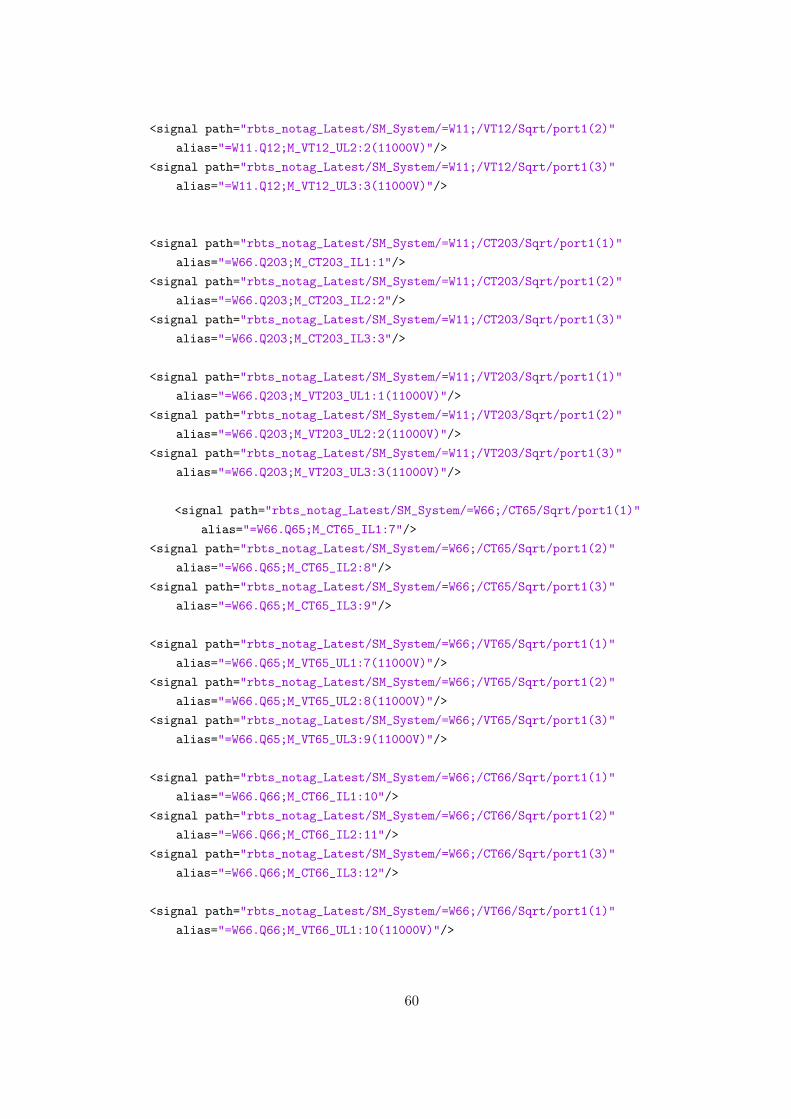
<signal path="rbts_notag_Latest/SM_System/=W11;/VT12/Sqrt/port1(2)"alias="=W11.Q12;M_VT12_UL2:2(11000V)"/>
<signal path="rbts_notag_Latest/SM_System/=W11;/VT12/Sqrt/port1(3)"alias="=W11.Q12;M_VT12_UL3:3(11000V)"/>
<signal path="rbts_notag_Latest/SM_System/=W11;/CT203/Sqrt/port1(1)"alias="=W66.Q203;M_CT203_IL1:1"/>
<signal path="rbts_notag_Latest/SM_System/=W11;/CT203/Sqrt/port1(2)"alias="=W66.Q203;M_CT203_IL2:2"/>
<signal path="rbts_notag_Latest/SM_System/=W11;/CT203/Sqrt/port1(3)"alias="=W66.Q203;M_CT203_IL3:3"/>
<signal path="rbts_notag_Latest/SM_System/=W11;/VT203/Sqrt/port1(1)"alias="=W66.Q203;M_VT203_UL1:1(11000V)"/>
<signal path="rbts_notag_Latest/SM_System/=W11;/VT203/Sqrt/port1(2)"alias="=W66.Q203;M_VT203_UL2:2(11000V)"/>
<signal path="rbts_notag_Latest/SM_System/=W11;/VT203/Sqrt/port1(3)"alias="=W66.Q203;M_VT203_UL3:3(11000V)"/>
<signal path="rbts_notag_Latest/SM_System/=W66;/CT65/Sqrt/port1(1)"alias="=W66.Q65;M_CT65_IL1:7"/>
<signal path="rbts_notag_Latest/SM_System/=W66;/CT65/Sqrt/port1(2)"alias="=W66.Q65;M_CT65_IL2:8"/>
<signal path="rbts_notag_Latest/SM_System/=W66;/CT65/Sqrt/port1(3)"alias="=W66.Q65;M_CT65_IL3:9"/>
<signal path="rbts_notag_Latest/SM_System/=W66;/VT65/Sqrt/port1(1)"alias="=W66.Q65;M_VT65_UL1:7(11000V)"/>
<signal path="rbts_notag_Latest/SM_System/=W66;/VT65/Sqrt/port1(2)"alias="=W66.Q65;M_VT65_UL2:8(11000V)"/>
<signal path="rbts_notag_Latest/SM_System/=W66;/VT65/Sqrt/port1(3)"alias="=W66.Q65;M_VT65_UL3:9(11000V)"/>
<signal path="rbts_notag_Latest/SM_System/=W66;/CT66/Sqrt/port1(1)"alias="=W66.Q66;M_CT66_IL1:10"/>
<signal path="rbts_notag_Latest/SM_System/=W66;/CT66/Sqrt/port1(2)"alias="=W66.Q66;M_CT66_IL2:11"/>
<signal path="rbts_notag_Latest/SM_System/=W66;/CT66/Sqrt/port1(3)"alias="=W66.Q66;M_CT66_IL3:12"/>
<signal path="rbts_notag_Latest/SM_System/=W66;/VT66/Sqrt/port1(1)"alias="=W66.Q66;M_VT66_UL1:10(11000V)"/>
60

<signal path="rbts_notag_Latest/SM_System/=W66;/VT66/Sqrt/port1(2)"alias="=W66.Q66;M_VT66_UL2:11(11000V)"/>
<signal path="rbts_notag_Latest/SM_System/=W66;/VT66/Sqrt/port1(3)"alias="=W66.Q66;M_VT66_UL3:12(11000V)"/>
<signal path="rbts_notag_Latest/SM_System/=W66;/CT67/Sqrt/port1(1)"alias="=W66.Q67;M_CT67_IL1:4"/>
<signal path="rbts_notag_Latest/SM_System/=W66;/CT67/Sqrt/port1(2)"alias="=W66.Q67;M_CT67_IL2:5"/>
<signal path="rbts_notag_Latest/SM_System/=W66;/CT67/Sqrt/port1(3)"alias="=W66.Q67;M_CT67_IL3:6"/>
<signal path="rbts_notag_Latest/SM_System/=W66;/VT67/Sqrt/port1(1)"alias="=W66.Q67;M_VT67_UL1:4(11000V)"/>
<signal path="rbts_notag_Latest/SM_System/=W66;/VT67/Sqrt/port1(2)"alias="=W66.Q67;M_VT67_UL2:5(11000V)"/>
<signal path="rbts_notag_Latest/SM_System/=W66;/VT67/Sqrt/port1(3)"alias="=W66.Q67;M_VT67_UL3:6(11000V)"/>
<signal path="rbts_notag_Latest/SM_System/=W64;/CT63/Sqrt/port1(1)"alias="=W64.Q63;M_CT63_IL1:1"/>
<signal path="rbts_notag_Latest/SM_System/=W64;/CT63/Sqrt/port1(2)"alias="=W64.Q63;M_CT63_IL2:2"/>
<signal path="rbts_notag_Latest/SM_System/=W64;/CT63/Sqrt/port1(3)"alias="=W64.Q63;M_CT63_IL3:3"/>
<signal path="rbts_notag_Latest/SM_System/=W64;/VT63/Sqrt/port1(1)"alias="=W64.Q63;M_VT63_UL1:1(11000V)"/>
<signal path="rbts_notag_Latest/SM_System/=W64;/VT63/Sqrt/port1(2)"alias="=W64.Q63;M_VT63_UL2:2(11000V)"/>
<signal path="rbts_notag_Latest/SM_System/=W64;/VT63/Sqrt/port1(3)"alias="=W64.Q63;M_VT63_UL3:3(11000V)"/>
<signal path="rbts_notag_Latest/SM_System/=W64;/CT64/Sqrt/port1(1)"alias="=W64.Q64;M_CT64_IL1:4"/>
<signal path="rbts_notag_Latest/SM_System/=W64;/CT64/Sqrt/port1(2)"alias="=W64.Q64;M_CT64_IL2:5"/>
<signal path="rbts_notag_Latest/SM_System/=W64;/CT64/Sqrt/port1(3)"alias="=W64.Q64;M_CT64_IL3:6"/>
<signal path="rbts_notag_Latest/SM_System/=W64;/VT64/Sqrt/port1(1)"alias="=W64.Q64;M_VT64_UL1:4(11000V)"/>
<signal path="rbts_notag_Latest/SM_System/=W64;/VT64/Sqrt/port1(2)"alias="=W64.Q64;M_VT64_UL2:5(11000V)"/>
61

<signal path="rbts_notag_Latest/SM_System/=W64;/VT64/Sqrt/port1(3)"alias="=W64.Q64;M_VT64_UL3:6(11000V)"/>
<signal path="rbts_notag_Latest/SM_System/=W61;/CT60/Sqrt/port1(1)"alias="=W61.Q60;M_CT60_IL1:13"/>
<signal path="rbts_notag_Latest/SM_System/=W61;/CT60/Sqrt/port1(2)"alias="=W61.Q60;M_CT60_IL2:14"/>
<signal path="rbts_notag_Latest/SM_System/=W61;/CT60/Sqrt/port1(3)"alias="=W61.Q60;M_CT60_IL3:15"/>
<signal path="rbts_notag_Latest/SM_System/=W61;/VT60/Sqrt/port1(1)"alias="=W61.Q60;M_VT60_UL1:13(11000V)"/>
<signal path="rbts_notag_Latest/SM_System/=W61;/VT60/Sqrt/port1(2)"alias="=W61.Q60;M_VT60_UL2:14(11000V)"/>
<signal path="rbts_notag_Latest/SM_System/=W61;/VT60/Sqrt/port1(3)"alias="=W61.Q60;M_VT60_UL3:15(11000V)"/>
<signal path="rbts_notag_Latest/SM_System/=W61;/CT61/Sqrt/port1(1)"alias="=W61.Q61;M_CT61_IL1:1"/>
<signal path="rbts_notag_Latest/SM_System/=W61;/CT61/Sqrt/port1(2)"alias="=W61.Q61;M_CT61_IL2:2"/>
<signal path="rbts_notag_Latest/SM_System/=W61;/CT61/Sqrt/port1(3)"alias="=W61.Q61;M_CT61_IL3:3"/>
<signal path="rbts_notag_Latest/SM_System/=W61;/VT61/Sqrt/port1(1)"alias="=W61.Q61;M_VT61_UL1:1(11000V)"/>
<signal path="rbts_notag_Latest/SM_System/=W61;/VT61/Sqrt/port1(2)"alias="=W61.Q61;M_VT61_UL2:2(11000V)"/>
<signal path="rbts_notag_Latest/SM_System/=W61;/VT61/Sqrt/port1(3)"alias="=W61.Q61;M_VT61_UL3:3(11000V)"/>
<signal path="rbts_notag_Latest/SM_System/=W61;/CT62/Sqrt/port1(1)"alias="=W61.Q62;M_CT62_IL1:7"/>
<signal path="rbts_notag_Latest/SM_System/=W61;/CT62/Sqrt/port1(2)"alias="=W61.Q62;M_CT62_IL2:8"/>
<signal path="rbts_notag_Latest/SM_System/=W61;/CT62/Sqrt/port1(3)"alias="=W61.Q62;M_CT62_IL3:9"/>
<signal path="rbts_notag_Latest/SM_System/=W61;/VT62/Sqrt/port1(1)"alias="=W61.Q62;M_VT62_UL1:7(11000V)"/>
<signal path="rbts_notag_Latest/SM_System/=W61;/VT62/Sqrt/port1(2)"alias="=W61.Q62;M_VT62_UL2:8(11000V)"/>
<signal path="rbts_notag_Latest/SM_System/=W61;/VT62/Sqrt/port1(3)"alias="=W61.Q62;M_VT62_UL3:9(11000V)"/>
62
<signal path="rbts_notag_Latest/SM_System/=W59;/CT58/Sqrt/port1(1)"alias="=W59.Q58;M_CT58_IL1:7"/>
<signal path="rbts_notag_Latest/SM_System/=W59;/CT58/Sqrt/port1(2)"alias="=W59.Q58;M_CT58_IL2:8"/>
<signal path="rbts_notag_Latest/SM_System/=W59;/CT58/Sqrt/port1(3)"alias="=W59.Q58;M_CT58_IL3:9"/>
<signal path="rbts_notag_Latest/SM_System/=W59;/VT58/Sqrt/port1(1)"alias="=W59.Q58;M_VT58_UL1:7(11000V)"/>
<signal path="rbts_notag_Latest/SM_System/=W59;/VT58/Sqrt/port1(2)"alias="=W59.Q58;M_VT58_UL2:8(11000V)"/>
<signal path="rbts_notag_Latest/SM_System/=W59;/VT58/Sqrt/port1(3)"alias="=W59.Q58;M_VT58_UL3:9(11000V)"/>
<signal path="rbts_notag_Latest/SM_System/=W59;/CT59/Sqrt/port1(1)"alias="=W59.Q59;M_CT59_IL1:1"/>
<signal path="rbts_notag_Latest/SM_System/=W59;/CT59/Sqrt/port1(2)"alias="=W59.Q59;M_CT59_IL2:2"/>
<signal path="rbts_notag_Latest/SM_System/=W59;/CT59/Sqrt/port1(3)"alias="=W59.Q59;M_CT59_IL3:3"/>
<signal path="rbts_notag_Latest/SM_System/=W59;/VT59/Sqrt/port1(1)"alias="=W59.Q59;M_VT59_UL1:1(11000V)"/>
<signal path="rbts_notag_Latest/SM_System/=W59;/VT59/Sqrt/port1(2)"alias="=W59.Q59;M_VT59_UL2:2(11000V)"/>
<signal path="rbts_notag_Latest/SM_System/=W59;/VT59/Sqrt/port1(3)"alias="=W59.Q59;M_VT59_UL3:3(11000V)"/>
<signal path="rbts_notag_Latest/SM_System/SS6/CT56/Sqrt/port1(1)"alias="=W1.Q56;M_CT56_IL1:1"/>
<signal path="rbts_notag_Latest/SM_System/SS6/CT56/Sqrt/port1(2)"alias="=W1.Q56;M_CT56_IL2:2"/>
<signal path="rbts_notag_Latest/SM_System/SS6/CT56/Sqrt/port1(3)"alias="=W1.Q56;M_CT56_IL3:3"/>
<signal path="rbts_notag_Latest/SM_System/SS6/VT56/Sqrt/port1(1)"alias="=W1.Q56;M_VT56_UL1:1(11000V)"/>
<signal path="rbts_notag_Latest/SM_System/SS6/VT56/Sqrt/port1(2)"alias="=W1.Q56;M_VT56_UL2:2(11000V)"/>
<signal path="rbts_notag_Latest/SM_System/SS6/VT56/Sqrt/port1(3)"alias="=W1.Q56;M_VT56_UL3:3(11000V)"/>
63
<signal path="rbts_notag_Latest/SM_System/=W58;/CT57/Sqrt/port1(1)"alias="=W58.Q57;M_CT57_IL1:7"/>
<signal path="rbts_notag_Latest/SM_System/=W58;/CT57/Sqrt/port1(2)"alias="=W58.Q57;M_CT57_IL2:8"/>
<signal path="rbts_notag_Latest/SM_System/=W58;/CT57/Sqrt/port1(3)"alias="=W58.Q57;M_CT57_IL3:9"/>
<signal path="rbts_notag_Latest/SM_System/=W58;/VT57/Sqrt/port1(1)"alias="=W58.Q57;M_VT57_UL1:7(11000V)"/>
<signal path="rbts_notag_Latest/SM_System/=W58;/VT57/Sqrt/port1(2)"alias="=W58.Q57;M_VT57_UL2:8(11000V)"/>
<signal path="rbts_notag_Latest/SM_System/=W58;/VT57/Sqrt/port1(3)"alias="=W58.Q57;M_VT57_UL3:9(11000V)"/>
<signal path="rbts_notag_Latest/SM_System/SS6/CT50/Sqrt/port1(1)"alias="=W1.Q50;M_CT50_IL1:4"/>
<signal path="rbts_notag_Latest/SM_System/SS6/CT50/Sqrt/port1(2)"alias="=W1.Q50;M_CT50_IL2:5"/>
<signal path="rbts_notag_Latest/SM_System/SS6/CT50/Sqrt/port1(3)"alias="=W1.Q50;M_CT50_IL3:6"/>
<signal path="rbts_notag_Latest/SM_System/SS6/VT50/Sqrt/port1(1)"alias="=W1.Q50;M_VT50_UL1:4(11000V)"/>
<signal path="rbts_notag_Latest/SM_System/SS6/VT50/Sqrt/port1(2)"alias="=W1.Q50;M_VT50_UL2:5(11000V)"/>
<signal path="rbts_notag_Latest/SM_System/SS6/VT50/Sqrt/port1(3)"alias="=W1.Q50;M_VT50_UL3:6(11000V)"/>
<signal path="rbts_notag_Latest/SM_System/=W52;/CT51/Sqrt/port1(1)"alias="=W52.Q51;M_CT51_IL1:1"/>
<signal path="rbts_notag_Latest/SM_System/=W52;/CT51/Sqrt/port1(2)"alias="=W52.Q51;M_CT51_IL2:2"/>
<signal path="rbts_notag_Latest/SM_System/=W52;/CT51/Sqrt/port1(3)"alias="=W52.Q51;M_CT51_IL3:3"/>
<signal path="rbts_notag_Latest/SM_System/=W52;/VT51/Sqrt/port1(1)"alias="=W52.Q51;M_VT51_UL1:1(11000V)"/>
<signal path="rbts_notag_Latest/SM_System/=W52;/VT51/Sqrt/port1(2)"alias="=W52.Q51;M_VT51_UL2:2(11000V)"/>
<signal path="rbts_notag_Latest/SM_System/=W52;/VT51/Sqrt/port1(3)"alias="=W52.Q51;M_VT51_UL3:3(11000V)"/>
<signal path="rbts_notag_Latest/SM_System/=W52;/CT52/Sqrt/port1(1)"alias="=W52.Q52;M_CT52_IL1:7"/>
64

<signal path="rbts_notag_Latest/SM_System/=W52;/CT52/Sqrt/port1(2)"alias="=W52.Q52;M_CT52_IL2:8"/>
<signal path="rbts_notag_Latest/SM_System/=W52;/CT52/Sqrt/port1(3)"alias="=W52.Q52;M_CT52_IL3:9"/>
<signal path="rbts_notag_Latest/SM_System/=W52;/VT52/Sqrt/port1(1)"alias="=W52.Q52;M_VT52_UL1:7(11000V)"/>
<signal path="rbts_notag_Latest/SM_System/=W52;/VT52/Sqrt/port1(2)"alias="=W52.Q52;M_VT52_UL2:8(11000V)"/>
<signal path="rbts_notag_Latest/SM_System/=W52;/VT52/Sqrt/port1(3)"alias="=W52.Q52;M_VT52_UL3:9(11000V)"/>
<signal path="rbts_notag_Latest/SM_System/=W53;/CT53/Sqrt/port1(1)"alias="=W53.Q53;M_CT53_IL1:7"/>
<signal path="rbts_notag_Latest/SM_System/=W53;/CT53/Sqrt/port1(2)"alias="=W53.Q53;M_CT53_IL2:8"/>
<signal path="rbts_notag_Latest/SM_System/=W53;/CT53/Sqrt/port1(3)"alias="=W53.Q53;M_CT53_IL3:9"/>
<signal path="rbts_notag_Latest/SM_System/=W53;/VT53/Sqrt/port1(1)"alias="=W53.Q53;M_VT53_UL1:7(11000V)"/>
<signal path="rbts_notag_Latest/SM_System/=W53;/VT53/Sqrt/port1(2)"alias="=W53.Q53;M_VT53_UL2:8(11000V)"/>
<signal path="rbts_notag_Latest/SM_System/=W53;/VT53/Sqrt/port1(3)"alias="=W53.Q53;M_VT53_UL3:9(11000V)"/>
<signal path="rbts_notag_Latest/SM_System/=W53;/CT54/Sqrt/port1(1)"alias="=W53.Q54;M_CT54_IL1:4"/>
<signal path="rbts_notag_Latest/SM_System/=W53;/CT54/Sqrt/port1(2)"alias="=W53.Q54;M_CT54_IL2:5"/>
<signal path="rbts_notag_Latest/SM_System/=W53;/CT54/Sqrt/port1(3)"alias="=W53.Q54;M_CT54_IL3:6"/>
<signal path="rbts_notag_Latest/SM_System/=W53;/VT54/Sqrt/port1(1)"alias="=W53.Q54;M_VT54_UL1:4(11000V)"/>
<signal path="rbts_notag_Latest/SM_System/=W53;/VT54/Sqrt/port1(2)"alias="=W53.Q54;M_VT54_UL2:5(11000V)"/>
<signal path="rbts_notag_Latest/SM_System/=W53;/VT54/Sqrt/port1(3)"alias="=W53.Q54;M_VT54_UL3:6(11000V)"/>
<signal path="rbts_notag_Latest/SM_System/=W55;/CT55/Sqrt/port1(1)"alias="=W55.Q55;M_CT55_IL1:7"/>
<signal path="rbts_notag_Latest/SM_System/=W55;/CT55/Sqrt/port1(2)"alias="=W55.Q55;M_CT55_IL2:8"/>
65
<signal path="rbts_notag_Latest/SM_System/=W55;/CT55/Sqrt/port1(3)"alias="=W55.Q55;M_CT55_IL3:9"/>
<signal path="rbts_notag_Latest/SM_System/=W55;/VT55/Sqrt/port1(1)"alias="=W55.Q55;M_VT55_UL1:7(11000V)"/>
<signal path="rbts_notag_Latest/SM_System/=W55;/VT55/Sqrt/port1(2)"alias="=W55.Q55;M_VT55_UL2:8(11000V)"/>
<signal path="rbts_notag_Latest/SM_System/=W55;/VT55/Sqrt/port1(3)"alias="=W55.Q55;M_VT55_UL3:9(11000V)"/>
<signal path="rbts_notag_Latest/SM_System/=W55;/CT201/Sqrt/port1(1)"alias="=W55.Q201;M_CT201_IL1:4"/>
<signal path="rbts_notag_Latest/SM_System/=W55;/CT201/Sqrt/port1(2)"alias="=W55.Q201;M_CT201_IL2:5"/>
<signal path="rbts_notag_Latest/SM_System/=W55;/CT201/Sqrt/port1(3)"alias="=W55.Q201;M_CT201_IL3:6"/>
<signal path="rbts_notag_Latest/SM_System/=W55;/VT201/Sqrt/port1(1)"alias="=W55.Q201;M_VT201_UL1:4(11000V)"/>
<signal path="rbts_notag_Latest/SM_System/=W55;/VT201/Sqrt/port1(2)"alias="=W55.Q201;M_VT201_UL2:5(11000V)"/>
<signal path="rbts_notag_Latest/SM_System/=W55;/VT201/Sqrt/port1(3)"alias="=W55.Q201;M_VT201_UL3:6(11000V)"/>
<signal path="rbts_notag_Latest/SM_System/=W18;/CT17/Sqrt/port1(1)"alias="=W18.Q17;M_CT17_IL1:7"/>
<signal path="rbts_notag_Latest/SM_System/=W18;/CT17/Sqrt/port1(2)"alias="=W18.Q17;M_CT17_IL2:8"/>
<signal path="rbts_notag_Latest/SM_System/=W18;/CT17/Sqrt/port1(3)"alias="=W18.Q17;M_CT17_IL3:9"/>
<signal path="rbts_notag_Latest/SM_System/=W18;/VT17/Sqrt/port1(1)"alias="=W18.Q17;M_VT17_UL1:7(11000V)"/>
<signal path="rbts_notag_Latest/SM_System/=W18;/VT17/Sqrt/port1(2)"alias="=W18.Q17;M_VT17_UL2:8(11000V)"/>
<signal path="rbts_notag_Latest/SM_System/=W18;/VT17/Sqrt/port1(3)"alias="=W18.Q17;M_VT17_UL3:9(11000V)"/>
<signal path="rbts_notag_Latest/SM_System/=W18;/CT18/Sqrt/port1(1)"alias="=W18.Q18;M_CT18_IL1:1"/>
<signal path="rbts_notag_Latest/SM_System/=W18;/CT18/Sqrt/port1(2)"alias="=W18.Q18;M_CT18_IL2:2"/>
66
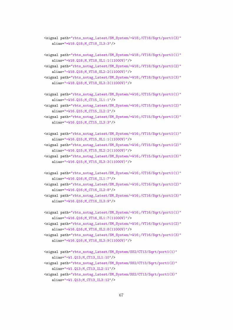
<signal path="rbts_notag_Latest/SM_System/=W18;/CT18/Sqrt/port1(3)"alias="=W18.Q18;M_CT18_IL3:3"/>
<signal path="rbts_notag_Latest/SM_System/=W18;/VT18/Sqrt/port1(1)"alias="=W18.Q18;M_VT18_UL1:1(11000V)"/>
<signal path="rbts_notag_Latest/SM_System/=W18;/VT18/Sqrt/port1(2)"alias="=W18.Q18;M_VT18_UL2:2(11000V)"/>
<signal path="rbts_notag_Latest/SM_System/=W18;/VT18/Sqrt/port1(3)"alias="=W18.Q18;M_VT18_UL3:3(11000V)"/>
<signal path="rbts_notag_Latest/SM_System/=W16;/CT15/Sqrt/port1(1)"alias="=W16.Q15;M_CT15_IL1:1"/>
<signal path="rbts_notag_Latest/SM_System/=W16;/CT15/Sqrt/port1(2)"alias="=W16.Q15;M_CT15_IL2:2"/>
<signal path="rbts_notag_Latest/SM_System/=W16;/CT15/Sqrt/port1(3)"alias="=W16.Q15;M_CT15_IL3:3"/>
<signal path="rbts_notag_Latest/SM_System/=W16;/VT15/Sqrt/port1(1)"alias="=W16.Q15;M_VT15_UL1:1(11000V)"/>
<signal path="rbts_notag_Latest/SM_System/=W16;/VT15/Sqrt/port1(2)"alias="=W16.Q15;M_VT15_UL2:2(11000V)"/>
<signal path="rbts_notag_Latest/SM_System/=W16;/VT15/Sqrt/port1(3)"alias="=W16.Q15;M_VT15_UL3:3(11000V)"/>
<signal path="rbts_notag_Latest/SM_System/=W16;/CT16/Sqrt/port1(1)"alias="=W16.Q16;M_CT16_IL1:7"/>
<signal path="rbts_notag_Latest/SM_System/=W16;/CT16/Sqrt/port1(2)"alias="=W16.Q16;M_CT16_IL2:8"/>
<signal path="rbts_notag_Latest/SM_System/=W16;/CT16/Sqrt/port1(3)"alias="=W16.Q16;M_CT16_IL3:9"/>
<signal path="rbts_notag_Latest/SM_System/=W16;/VT16/Sqrt/port1(1)"alias="=W16.Q16;M_VT16_UL1:7(11000V)"/>
<signal path="rbts_notag_Latest/SM_System/=W16;/VT16/Sqrt/port1(2)"alias="=W16.Q16;M_VT16_UL2:8(11000V)"/>
<signal path="rbts_notag_Latest/SM_System/=W16;/VT16/Sqrt/port1(3)"alias="=W16.Q16;M_VT16_UL3:9(11000V)"/>
<signal path="rbts_notag_Latest/SM_System/SS2/CT13/Sqrt/port1(1)"alias="=W1.Q13;M_CT13_IL1:10"/>
<signal path="rbts_notag_Latest/SM_System/SS2/CT13/Sqrt/port1(2)"alias="=W1.Q13;M_CT13_IL2:11"/>
<signal path="rbts_notag_Latest/SM_System/SS2/CT13/Sqrt/port1(3)"alias="=W1.Q13;M_CT13_IL3:12"/>
67

<signal path="rbts_notag_Latest/SM_System/SS2/VT13/Sqrt/port1(1)"alias="=W1.Q13;M_VT13_UL1:10(11000V)"/>
<signal path="rbts_notag_Latest/SM_System/SS2/VT13/Sqrt/port1(2)"alias="=W1.Q13;M_VT13_UL2:11(11000V)"/>
<signal path="rbts_notag_Latest/SM_System/SS2/VT13/Sqrt/port1(3)"alias="=W1.Q13;M_VT13_UL3:12(11000V)"/>
<signal path="rbts_notag_Latest/SM_System/=W15;/CT14/Sqrt/port1(1)"alias="=W15.Q14;M_CT14_IL1:7"/>
<signal path="rbts_notag_Latest/SM_System/=W15;/CT14/Sqrt/port1(2)"alias="=W15.Q14;M_CT14_IL2:8"/>
<signal path="rbts_notag_Latest/SM_System/=W15;/CT14/Sqrt/port1(3)"alias="=W15.Q14;M_CT14_IL3:9"/>
<signal path="rbts_notag_Latest/SM_System/=W15;/VT14/Sqrt/port1(1)"alias="=W15.Q14;M_VT14_UL1:7(11000V)"/>
<signal path="rbts_notag_Latest/SM_System/=W15;/VT14/Sqrt/port1(2)"alias="=W15.Q14;M_VT14_UL2:8(11000V)"/>
<signal path="rbts_notag_Latest/SM_System/=W15;/VT14/Sqrt/port1(3)"alias="=W15.Q14;M_VT14_UL3:9(11000V)"/>
<signal path="rbts_notag_Latest/SM_System/SS2/CT19/Sqrt/port1(1)"alias="=W1.Q19;M_CT19_IL1:4"/>
<signal path="rbts_notag_Latest/SM_System/SS2/CT19/Sqrt/port1(2)"alias="=W1.Q19;M_CT19_IL2:5"/>
<signal path="rbts_notag_Latest/SM_System/SS2/CT19/Sqrt/port1(3)"alias="=W1.Q19;M_CT19_IL3:6"/>
<signal path="rbts_notag_Latest/SM_System/SS2/VT19/Sqrt/port1(1)"alias="=W1.Q19;M_VT19_UL1:4(11000V)"/>
<signal path="rbts_notag_Latest/SM_System/SS2/VT19/Sqrt/port1(2)"alias="=W1.Q19;M_VT19_UL2:5(11000V)"/>
<signal path="rbts_notag_Latest/SM_System/SS2/VT19/Sqrt/port1(3)"alias="=W1.Q19;M_VT19_UL3:6(11000V)"/>
<signal path="rbts_notag_Latest/SM_System/=W21;/CT20/Sqrt/port1(1)"alias="=W21.Q20;M_CT20_IL1:7"/>
<signal path="rbts_notag_Latest/SM_System/=W21;/CT20/Sqrt/port1(2)"alias="=W21.Q20;M_CT20_IL2:8"/>
<signal path="rbts_notag_Latest/SM_System/=W21;/CT20/Sqrt/port1(3)"alias="=W21.Q20;M_CT20_IL3:9"/>
68

<signal path="rbts_notag_Latest/SM_System/=W21;/VT20/Sqrt/port1(1)"alias="=W21.Q20;M_VT20_UL1:7(11000V)"/>
<signal path="rbts_notag_Latest/SM_System/=W21;/VT20/Sqrt/port1(2)"alias="=W21.Q20;M_VT20_UL2:8(11000V)"/>
<signal path="rbts_notag_Latest/SM_System/=W21;/VT20/Sqrt/port1(3)"alias="=W21.Q20;M_VT20_UL3:9(11000V)"/>
<signal path="rbts_notag_Latest/SM_System/=W21;/CT21/Sqrt/port1(1)"alias="=W21.Q21;M_CT21_IL1:4"/>
<signal path="rbts_notag_Latest/SM_System/=W21;/CT21/Sqrt/port1(2)"alias="=W21.Q21;M_CT21_IL2:5"/>
<signal path="rbts_notag_Latest/SM_System/=W21;/CT21/Sqrt/port1(3)"alias="=W21.Q21;M_CT21_IL3:6"/>
<signal path="rbts_notag_Latest/SM_System/=W21;/VT21/Sqrt/port1(1)"alias="=W21.Q21;M_VT21_UL1:4(11000V)"/>
<signal path="rbts_notag_Latest/SM_System/=W21;/VT21/Sqrt/port1(2)"alias="=W21.Q21;M_VT21_UL2:5(11000V)"/>
<signal path="rbts_notag_Latest/SM_System/=W21;/VT21/Sqrt/port1(3)"alias="=W21.Q21;M_VT21_UL3:6(11000V)"/>
<signal path="rbts_notag_Latest/SM_System/=W22;/CT22/Sqrt/port1(1)"alias="=W22.Q22;M_CT22_IL1:1"/>
<signal path="rbts_notag_Latest/SM_System/=W22;/CT22/Sqrt/port1(2)"alias="=W22.Q22;M_CT22_IL2:2"/>
<signal path="rbts_notag_Latest/SM_System/=W22;/CT22/Sqrt/port1(3)"alias="=W22.Q22;M_CT22_IL3:3"/>
<signal path="rbts_notag_Latest/SM_System/=W22;/VT22/Sqrt/port1(1)"alias="=W22.Q22;M_VT22_UL1:1(11000V)"/>
<signal path="rbts_notag_Latest/SM_System/=W22;/VT22/Sqrt/port1(2)"alias="=W22.Q22;M_VT22_UL2:2(11000V)"/>
<signal path="rbts_notag_Latest/SM_System/=W22;/VT22/Sqrt/port1(3)"alias="=W22.Q22;M_VT22_UL3:3(11000V)"/>
<signal path="rbts_notag_Latest/SM_System/=W22;/CT23/Sqrt/port1(1)"alias="=W22.Q23;M_CT23_IL1:7"/>
<signal path="rbts_notag_Latest/SM_System/=W22;/CT23/Sqrt/port1(2)"alias="=W22.Q23;M_CT23_IL2:8"/>
<signal path="rbts_notag_Latest/SM_System/=W22;/CT23/Sqrt/port1(3)"alias="=W22.Q23;M_CT23_IL3:9"/>
<signal path="rbts_notag_Latest/SM_System/=W22;/VT23/Sqrt/port1(1)"alias="=W22.Q23;M_VT23_UL1:7(11000V)"/>
69
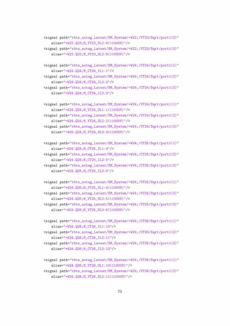
<signal path="rbts_notag_Latest/SM_System/=W22;/VT23/Sqrt/port1(2)"alias="=W22.Q23;M_VT23_UL2:8(11000V)"/>
<signal path="rbts_notag_Latest/SM_System/=W22;/VT23/Sqrt/port1(3)"alias="=W22.Q23;M_VT23_UL3:9(11000V)"/>
<signal path="rbts_notag_Latest/SM_System/=W24;/CT24/Sqrt/port1(1)"alias="=W24.Q24;M_CT24_IL1:1"/>
<signal path="rbts_notag_Latest/SM_System/=W24;/CT24/Sqrt/port1(2)"alias="=W24.Q24;M_CT24_IL2:2"/>
<signal path="rbts_notag_Latest/SM_System/=W24;/CT24/Sqrt/port1(3)"alias="=W24.Q24;M_CT24_IL3:3"/>
<signal path="rbts_notag_Latest/SM_System/=W24;/VT24/Sqrt/port1(1)"alias="=W24.Q24;M_VT24_UL1:1(11000V)"/>
<signal path="rbts_notag_Latest/SM_System/=W24;/VT24/Sqrt/port1(2)"alias="=W24.Q24;M_VT24_UL2:2(11000V)"/>
<signal path="rbts_notag_Latest/SM_System/=W24;/VT24/Sqrt/port1(3)"alias="=W24.Q24;M_VT24_UL3:3(11000V)"/>
<signal path="rbts_notag_Latest/SM_System/=W24;/CT25/Sqrt/port1(1)"alias="=W24.Q25;M_CT25_IL1:4"/>
<signal path="rbts_notag_Latest/SM_System/=W24;/CT25/Sqrt/port1(2)"alias="=W24.Q25;M_CT25_IL2:5"/>
<signal path="rbts_notag_Latest/SM_System/=W24;/CT25/Sqrt/port1(3)"alias="=W24.Q25;M_CT25_IL3:6"/>
<signal path="rbts_notag_Latest/SM_System/=W24;/VT25/Sqrt/port1(1)"alias="=W24.Q25;M_VT25_UL1:4(11000V)"/>
<signal path="rbts_notag_Latest/SM_System/=W24;/VT25/Sqrt/port1(2)"alias="=W24.Q25;M_VT25_UL2:5(11000V)"/>
<signal path="rbts_notag_Latest/SM_System/=W24;/VT25/Sqrt/port1(3)"alias="=W24.Q25;M_VT25_UL3:6(11000V)"/>
<signal path="rbts_notag_Latest/SM_System/=W24;/CT26/Sqrt/port1(1)"alias="=W24.Q26;M_CT26_IL1:10"/>
<signal path="rbts_notag_Latest/SM_System/=W24;/CT26/Sqrt/port1(2)"alias="=W24.Q26;M_CT26_IL2:11"/>
<signal path="rbts_notag_Latest/SM_System/=W24;/CT26/Sqrt/port1(3)"alias="=W24.Q26;M_CT26_IL3:12"/>
<signal path="rbts_notag_Latest/SM_System/=W24;/VT26/Sqrt/port1(1)"alias="=W24.Q26;M_VT26_UL1:10(11000V)"/>
<signal path="rbts_notag_Latest/SM_System/=W24;/VT26/Sqrt/port1(2)"alias="=W24.Q26;M_VT26_UL2:11(11000V)"/>
70

<signal path="rbts_notag_Latest/SM_System/=W24;/VT26/Sqrt/port1(3)"alias="=W24.Q26;M_VT26_UL3:12(11000V)"/>
<signal path="rbts_notag_Latest/SM_System/=W27;/CT27/Sqrt/port1(1)"alias="=W27.Q27;M_CT27_IL1:7"/>
<signal path="rbts_notag_Latest/SM_System/=W27;/CT27/Sqrt/port1(2)"alias="=W27.Q27;M_CT27_IL2:8"/>
<signal path="rbts_notag_Latest/SM_System/=W27;/CT27/Sqrt/port1(3)"alias="=W27.Q27;M_CT27_IL3:9"/>
<signal path="rbts_notag_Latest/SM_System/=W27;/VT27/Sqrt/port1(1)"alias="=W27.Q27;M_VT27_UL1:7(11000V)"/>
<signal path="rbts_notag_Latest/SM_System/=W27;/VT27/Sqrt/port1(2)"alias="=W27.Q27;M_VT27_UL2:8(11000V)"/>
<signal path="rbts_notag_Latest/SM_System/=W27;/VT27/Sqrt/port1(3)"alias="=W27.Q27;M_VT27_UL3:9(11000V)"/>
<signal path="rbts_notag_Latest/SM_System/=W27;/CT28/Sqrt/port1(1)"alias="=W27.Q28;M_CT28_IL1:1"/>
<signal path="rbts_notag_Latest/SM_System/=W27;/CT28/Sqrt/port1(2)"alias="=W27.Q28;M_CT28_IL2:2"/>
<signal path="rbts_notag_Latest/SM_System/=W27;/CT28/Sqrt/port1(3)"alias="=W27.Q28;M_CT28_IL3:3"/>
<signal path="rbts_notag_Latest/SM_System/=W27;/VT28/Sqrt/port1(1)"alias="=W27.Q28;M_VT28_UL1:1(11000V)"/>
<signal path="rbts_notag_Latest/SM_System/=W27;/VT28/Sqrt/port1(2)"alias="=W27.Q28;M_VT28_UL2:2(11000V)"/>
<signal path="rbts_notag_Latest/SM_System/=W27;/VT28/Sqrt/port1(3)"alias="=W27.Q28;M_VT28_UL3:3(11000V)"/>
<signal path="rbts_notag_Latest/SM_System/=W29;/CT29/Sqrt/port1(1)"alias="=W29.Q29;M_CT29_IL1:1"/>
<signal path="rbts_notag_Latest/SM_System/=W29;/CT29/Sqrt/port1(2)"alias="=W29.Q29;M_CT29_IL2:2"/>
<signal path="rbts_notag_Latest/SM_System/=W29;/CT29/Sqrt/port1(3)"alias="=W29.Q29;M_CT29_IL3:3"/>
<signal path="rbts_notag_Latest/SM_System/=W29;/VT29/Sqrt/port1(1)"alias="=W29.Q29;M_VT29_UL1:1(11000V)"/>
<signal path="rbts_notag_Latest/SM_System/=W29;/VT29/Sqrt/port1(2)"alias="=W29.Q29;M_VT29_UL2:2(11000V)"/>
<signal path="rbts_notag_Latest/SM_System/=W29;/VT29/Sqrt/port1(3)"alias="=W29.Q29;M_VT29_UL3:3(11000V)"/>
71
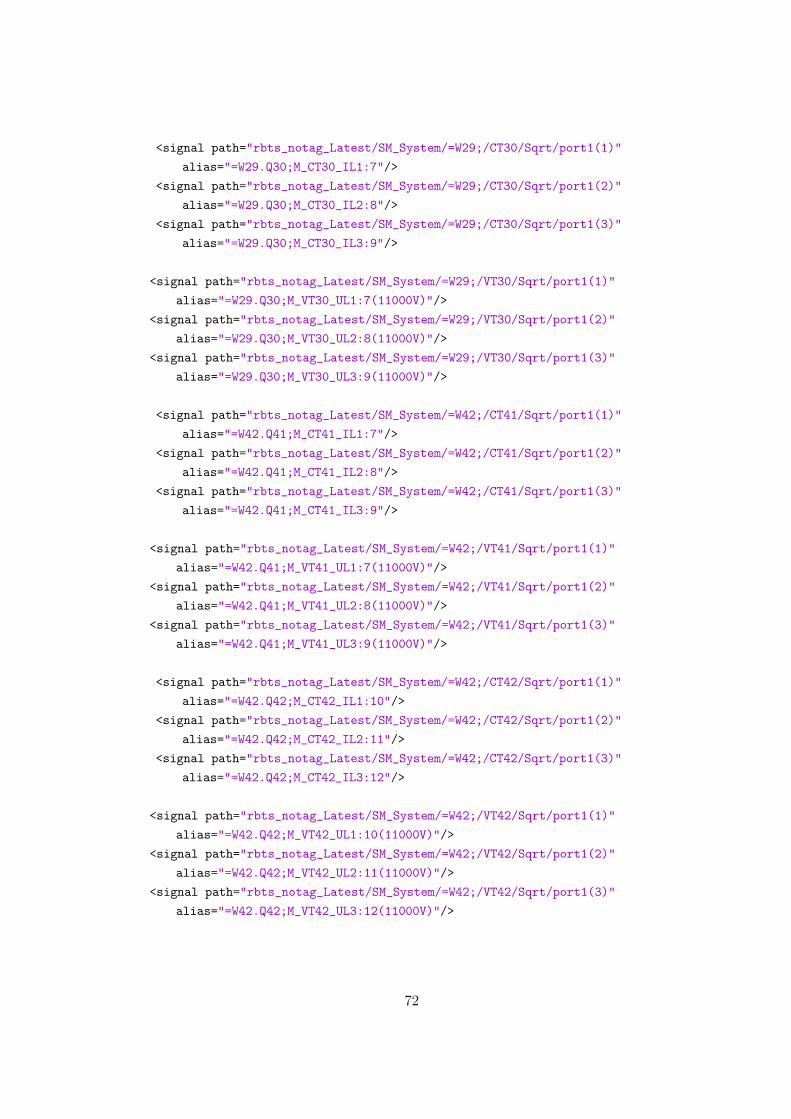
<signal path="rbts_notag_Latest/SM_System/=W29;/CT30/Sqrt/port1(1)"alias="=W29.Q30;M_CT30_IL1:7"/>
<signal path="rbts_notag_Latest/SM_System/=W29;/CT30/Sqrt/port1(2)"alias="=W29.Q30;M_CT30_IL2:8"/>
<signal path="rbts_notag_Latest/SM_System/=W29;/CT30/Sqrt/port1(3)"alias="=W29.Q30;M_CT30_IL3:9"/>
<signal path="rbts_notag_Latest/SM_System/=W29;/VT30/Sqrt/port1(1)"alias="=W29.Q30;M_VT30_UL1:7(11000V)"/>
<signal path="rbts_notag_Latest/SM_System/=W29;/VT30/Sqrt/port1(2)"alias="=W29.Q30;M_VT30_UL2:8(11000V)"/>
<signal path="rbts_notag_Latest/SM_System/=W29;/VT30/Sqrt/port1(3)"alias="=W29.Q30;M_VT30_UL3:9(11000V)"/>
<signal path="rbts_notag_Latest/SM_System/=W42;/CT41/Sqrt/port1(1)"alias="=W42.Q41;M_CT41_IL1:7"/>
<signal path="rbts_notag_Latest/SM_System/=W42;/CT41/Sqrt/port1(2)"alias="=W42.Q41;M_CT41_IL2:8"/>
<signal path="rbts_notag_Latest/SM_System/=W42;/CT41/Sqrt/port1(3)"alias="=W42.Q41;M_CT41_IL3:9"/>
<signal path="rbts_notag_Latest/SM_System/=W42;/VT41/Sqrt/port1(1)"alias="=W42.Q41;M_VT41_UL1:7(11000V)"/>
<signal path="rbts_notag_Latest/SM_System/=W42;/VT41/Sqrt/port1(2)"alias="=W42.Q41;M_VT41_UL2:8(11000V)"/>
<signal path="rbts_notag_Latest/SM_System/=W42;/VT41/Sqrt/port1(3)"alias="=W42.Q41;M_VT41_UL3:9(11000V)"/>
<signal path="rbts_notag_Latest/SM_System/=W42;/CT42/Sqrt/port1(1)"alias="=W42.Q42;M_CT42_IL1:10"/>
<signal path="rbts_notag_Latest/SM_System/=W42;/CT42/Sqrt/port1(2)"alias="=W42.Q42;M_CT42_IL2:11"/>
<signal path="rbts_notag_Latest/SM_System/=W42;/CT42/Sqrt/port1(3)"alias="=W42.Q42;M_CT42_IL3:12"/>
<signal path="rbts_notag_Latest/SM_System/=W42;/VT42/Sqrt/port1(1)"alias="=W42.Q42;M_VT42_UL1:10(11000V)"/>
<signal path="rbts_notag_Latest/SM_System/=W42;/VT42/Sqrt/port1(2)"alias="=W42.Q42;M_VT42_UL2:11(11000V)"/>
<signal path="rbts_notag_Latest/SM_System/=W42;/VT42/Sqrt/port1(3)"alias="=W42.Q42;M_VT42_UL3:12(11000V)"/>
72

<signal path="rbts_notag_Latest/SM_System/=W42;/CT43/Sqrt/port1(1)"alias="=W42.Q43;M_CT43_IL1:4"/>
<signal path="rbts_notag_Latest/SM_System/=W42;/CT43/Sqrt/port1(2)"alias="=W42.Q43;M_CT43_IL2:5"/>
<signal path="rbts_notag_Latest/SM_System/=W42;/CT43/Sqrt/port1(3)"alias="=W42.Q43;M_CT43_IL3:6"/>
<signal path="rbts_notag_Latest/SM_System/=W42;/VT43/Sqrt/port1(1)"alias="=W42.Q43;M_VT43_UL1:4(11000V)"/>
<signal path="rbts_notag_Latest/SM_System/=W42;/VT43/Sqrt/port1(2)"alias="=W42.Q43;M_VT43_UL2:5(11000V)"/>
<signal path="rbts_notag_Latest/SM_System/=W42;/VT43/Sqrt/port1(3)"alias="=W42.Q43;M_VT43_UL3:6(11000V)"/>
<signal path="rbts_notag_Latest/SM_System/=W40;/CT39/Sqrt/port1(1)"alias="=W40.Q39;M_CT39_IL1:10"/>
<signal path="rbts_notag_Latest/SM_System/=W40;/CT39/Sqrt/port1(2)"alias="=W40.Q39;M_CT39_IL2:11"/>
<signal path="rbts_notag_Latest/SM_System/=W40;/CT39/Sqrt/port1(3)"alias="=W40.Q39;M_CT39_IL3:12"/>
<signal path="rbts_notag_Latest/SM_System/=W40;/VT39/Sqrt/port1(1)"alias="=W40.Q39;M_VT39_UL1:10(11000V)"/>
<signal path="rbts_notag_Latest/SM_System/=W40;/VT39/Sqrt/port1(2)"alias="=W40.Q39;M_VT39_UL2:11(11000V)"/>
<signal path="rbts_notag_Latest/SM_System/=W40;/VT39/Sqrt/port1(3)"alias="=W40.Q39;M_VT39_UL3:12(11000V)"/>
<signal path="rbts_notag_Latest/SM_System/=W40;/CT40/Sqrt/port1(1)"alias="=W40.Q40;M_CT40_IL1:1"/>
<signal path="rbts_notag_Latest/SM_System/=W40;/CT40/Sqrt/port1(2)"alias="=W40.Q40;M_CT40_IL2:2"/>
<signal path="rbts_notag_Latest/SM_System/=W40;/CT40/Sqrt/port1(3)"alias="=W40.Q40;M_CT40_IL3:3"/>
<signal path="rbts_notag_Latest/SM_System/=W40;/VT40/Sqrt/port1(1)"alias="=W40.Q40;M_VT40_UL1:1(11000V)"/>
<signal path="rbts_notag_Latest/SM_System/=W40;/VT40/Sqrt/port1(2)"alias="=W40.Q40;M_VT40_UL2:2(11000V)"/>
<signal path="rbts_notag_Latest/SM_System/=W40;/VT40/Sqrt/port1(3)"alias="=W40.Q40;M_VT40_UL3:3(11000V)"/>
<signal path="rbts_notag_Latest/SM_System/=W37;/CT36/Sqrt/port1(1)"alias="=W37.Q36;M_CT36_IL1:4"/>
73
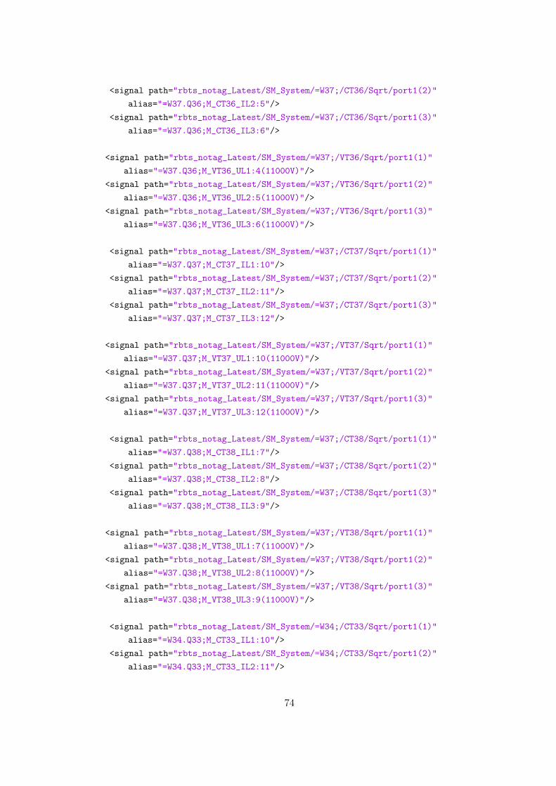
<signal path="rbts_notag_Latest/SM_System/=W37;/CT36/Sqrt/port1(2)"alias="=W37.Q36;M_CT36_IL2:5"/>
<signal path="rbts_notag_Latest/SM_System/=W37;/CT36/Sqrt/port1(3)"alias="=W37.Q36;M_CT36_IL3:6"/>
<signal path="rbts_notag_Latest/SM_System/=W37;/VT36/Sqrt/port1(1)"alias="=W37.Q36;M_VT36_UL1:4(11000V)"/>
<signal path="rbts_notag_Latest/SM_System/=W37;/VT36/Sqrt/port1(2)"alias="=W37.Q36;M_VT36_UL2:5(11000V)"/>
<signal path="rbts_notag_Latest/SM_System/=W37;/VT36/Sqrt/port1(3)"alias="=W37.Q36;M_VT36_UL3:6(11000V)"/>
<signal path="rbts_notag_Latest/SM_System/=W37;/CT37/Sqrt/port1(1)"alias="=W37.Q37;M_CT37_IL1:10"/>
<signal path="rbts_notag_Latest/SM_System/=W37;/CT37/Sqrt/port1(2)"alias="=W37.Q37;M_CT37_IL2:11"/>
<signal path="rbts_notag_Latest/SM_System/=W37;/CT37/Sqrt/port1(3)"alias="=W37.Q37;M_CT37_IL3:12"/>
<signal path="rbts_notag_Latest/SM_System/=W37;/VT37/Sqrt/port1(1)"alias="=W37.Q37;M_VT37_UL1:10(11000V)"/>
<signal path="rbts_notag_Latest/SM_System/=W37;/VT37/Sqrt/port1(2)"alias="=W37.Q37;M_VT37_UL2:11(11000V)"/>
<signal path="rbts_notag_Latest/SM_System/=W37;/VT37/Sqrt/port1(3)"alias="=W37.Q37;M_VT37_UL3:12(11000V)"/>
<signal path="rbts_notag_Latest/SM_System/=W37;/CT38/Sqrt/port1(1)"alias="=W37.Q38;M_CT38_IL1:7"/>
<signal path="rbts_notag_Latest/SM_System/=W37;/CT38/Sqrt/port1(2)"alias="=W37.Q38;M_CT38_IL2:8"/>
<signal path="rbts_notag_Latest/SM_System/=W37;/CT38/Sqrt/port1(3)"alias="=W37.Q38;M_CT38_IL3:9"/>
<signal path="rbts_notag_Latest/SM_System/=W37;/VT38/Sqrt/port1(1)"alias="=W37.Q38;M_VT38_UL1:7(11000V)"/>
<signal path="rbts_notag_Latest/SM_System/=W37;/VT38/Sqrt/port1(2)"alias="=W37.Q38;M_VT38_UL2:8(11000V)"/>
<signal path="rbts_notag_Latest/SM_System/=W37;/VT38/Sqrt/port1(3)"alias="=W37.Q38;M_VT38_UL3:9(11000V)"/>
<signal path="rbts_notag_Latest/SM_System/=W34;/CT33/Sqrt/port1(1)"alias="=W34.Q33;M_CT33_IL1:10"/>
<signal path="rbts_notag_Latest/SM_System/=W34;/CT33/Sqrt/port1(2)"alias="=W34.Q33;M_CT33_IL2:11"/>
74

<signal path="rbts_notag_Latest/SM_System/=W34;/CT33/Sqrt/port1(3)"alias="=W34.Q33;M_CT33_IL3:12"/>
<signal path="rbts_notag_Latest/SM_System/=W34;/VT33/Sqrt/port1(1)"alias="=W34.Q33;M_VT33_UL1:10(11000V)"/>
<signal path="rbts_notag_Latest/SM_System/=W34;/VT33/Sqrt/port1(2)"alias="=W34.Q33;M_VT33_UL2:11(11000V)"/>
<signal path="rbts_notag_Latest/SM_System/=W34;/VT33/Sqrt/port1(3)"alias="=W34.Q33;M_VT33_UL3:12(11000V)"/>
<signal path="rbts_notag_Latest/SM_System/=W34;/CT34/Sqrt/port1(1)"alias="=W34.Q34;M_CT34_IL1:4"/>
<signal path="rbts_notag_Latest/SM_System/=W34;/CT34/Sqrt/port1(2)"alias="=W34.Q34;M_CT34_IL2:5"/>
<signal path="rbts_notag_Latest/SM_System/=W34;/CT34/Sqrt/port1(3)"alias="=W34.Q34;M_CT34_IL3:6"/>
<signal path="rbts_notag_Latest/SM_System/=W34;/VT34/Sqrt/port1(1)"alias="=W34.Q34;M_VT34_UL1:4(11000V)"/>
<signal path="rbts_notag_Latest/SM_System/=W34;/VT34/Sqrt/port1(2)"alias="=W34.Q34;M_VT34_UL2:5(11000V)"/>
<signal path="rbts_notag_Latest/SM_System/=W34;/VT34/Sqrt/port1(3)"alias="=W34.Q34;M_VT34_UL3:6(11000V)"/>
<signal path="rbts_notag_Latest/SM_System/=W34;/CT35/Sqrt/port1(1)"alias="=W34.Q35;M_CT35_IL1:1"/>
<signal path="rbts_notag_Latest/SM_System/=W34;/CT35/Sqrt/port1(2)"alias="=W34.Q35;M_CT35_IL2:2"/>
<signal path="rbts_notag_Latest/SM_System/=W34;/CT35/Sqrt/port1(3)"alias="=W34.Q35;M_CT35_IL3:3"/>
<signal path="rbts_notag_Latest/SM_System/=W34;/VT35/Sqrt/port1(1)"alias="=W34.Q35;M_VT35_UL1:1(11000V)"/>
<signal path="rbts_notag_Latest/SM_System/=W34;/VT35/Sqrt/port1(2)"alias="=W34.Q35;M_VT35_UL2:2(11000V)"/>
<signal path="rbts_notag_Latest/SM_System/=W34;/VT35/Sqrt/port1(3)"alias="=W34.Q35;M_VT35_UL3:3(11000V)"/>
<signal path="rbts_notag_Latest/SM_System/SS4/CT31/Sqrt/port1(1)"alias="=W1.Q31;M_CT31_IL1:1"/>
<signal path="rbts_notag_Latest/SM_System/SS4/CT31/Sqrt/port1(2)"alias="=W1.Q31;M_CT31_IL2:2"/>
<signal path="rbts_notag_Latest/SM_System/SS4/CT31/Sqrt/port1(3)"alias="=W1.Q31;M_CT31_IL3:3"/>
75
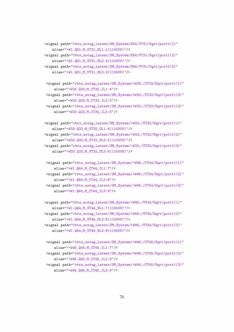
<signal path="rbts_notag_Latest/SM_System/SS4/VT31/Sqrt/port1(1)"alias="=W1.Q31;M_VT31_UL1:1(11000V)"/>
<signal path="rbts_notag_Latest/SM_System/SS4/VT31/Sqrt/port1(2)"alias="=W1.Q31;M_VT31_UL2:2(11000V)"/>
<signal path="rbts_notag_Latest/SM_System/SS4/VT31/Sqrt/port1(3)"alias="=W1.Q31;M_VT31_UL3:3(11000V)"/>
<signal path="rbts_notag_Latest/SM_System/=W33;/CT32/Sqrt/port1(1)"alias="=W33.Q32;M_CT32_IL1:4"/>
<signal path="rbts_notag_Latest/SM_System/=W33;/CT32/Sqrt/port1(2)"alias="=W33.Q32;M_CT32_IL2:5"/>
<signal path="rbts_notag_Latest/SM_System/=W33;/CT32/Sqrt/port1(3)"alias="=W33.Q32;M_CT32_IL3:6"/>
<signal path="rbts_notag_Latest/SM_System/=W33;/VT32/Sqrt/port1(1)"alias="=W33.Q32;M_VT32_UL1:4(11000V)"/>
<signal path="rbts_notag_Latest/SM_System/=W33;/VT32/Sqrt/port1(2)"alias="=W33.Q32;M_VT32_UL2:5(11000V)"/>
<signal path="rbts_notag_Latest/SM_System/=W33;/VT32/Sqrt/port1(3)"alias="=W33.Q32;M_VT32_UL3:6(11000V)"/>
<signal path="rbts_notag_Latest/SM_System/=W46;/CT44/Sqrt/port1(1)"alias="=W1.Q44;M_CT44_IL1:7"/>
<signal path="rbts_notag_Latest/SM_System/=W46;/CT44/Sqrt/port1(2)"alias="=W1.Q44;M_CT44_IL2:8"/>
<signal path="rbts_notag_Latest/SM_System/=W46;/CT44/Sqrt/port1(3)"alias="=W1.Q44;M_CT44_IL3:9"/>
<signal path="rbts_notag_Latest/SM_System/=W46;/VT44/Sqrt/port1(1)"alias="=W1.Q44;M_VT44_UL1:7(11000V)"/>
<signal path="rbts_notag_Latest/SM_System/=W46;/VT44/Sqrt/port1(2)"alias="=W1.Q44;M_VT44_UL2:8(11000V)"/>
<signal path="rbts_notag_Latest/SM_System/=W46;/VT44/Sqrt/port1(3)"alias="=W1.Q44;M_VT44_UL3:9(11000V)"/>
<signal path="rbts_notag_Latest/SM_System/=W46;/CT45/Sqrt/port1(1)"alias="=W46.Q45;M_CT45_IL1:7"/>
<signal path="rbts_notag_Latest/SM_System/=W46;/CT45/Sqrt/port1(2)"alias="=W46.Q45;M_CT45_IL2:8"/>
<signal path="rbts_notag_Latest/SM_System/=W46;/CT45/Sqrt/port1(3)"alias="=W46.Q45;M_CT45_IL3:9"/>
76
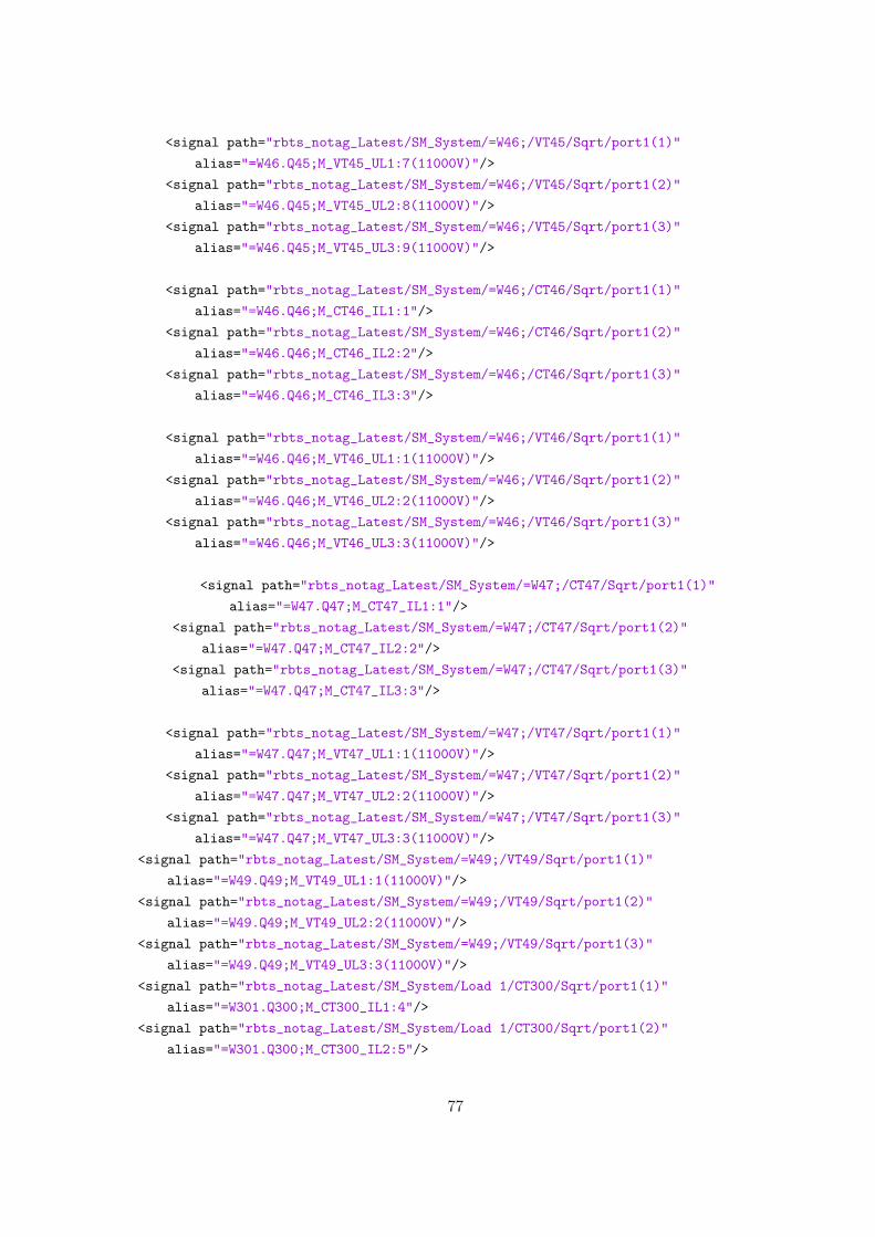
<signal path="rbts_notag_Latest/SM_System/=W46;/VT45/Sqrt/port1(1)"alias="=W46.Q45;M_VT45_UL1:7(11000V)"/>
<signal path="rbts_notag_Latest/SM_System/=W46;/VT45/Sqrt/port1(2)"alias="=W46.Q45;M_VT45_UL2:8(11000V)"/>
<signal path="rbts_notag_Latest/SM_System/=W46;/VT45/Sqrt/port1(3)"alias="=W46.Q45;M_VT45_UL3:9(11000V)"/>
<signal path="rbts_notag_Latest/SM_System/=W46;/CT46/Sqrt/port1(1)"alias="=W46.Q46;M_CT46_IL1:1"/>
<signal path="rbts_notag_Latest/SM_System/=W46;/CT46/Sqrt/port1(2)"alias="=W46.Q46;M_CT46_IL2:2"/>
<signal path="rbts_notag_Latest/SM_System/=W46;/CT46/Sqrt/port1(3)"alias="=W46.Q46;M_CT46_IL3:3"/>
<signal path="rbts_notag_Latest/SM_System/=W46;/VT46/Sqrt/port1(1)"alias="=W46.Q46;M_VT46_UL1:1(11000V)"/>
<signal path="rbts_notag_Latest/SM_System/=W46;/VT46/Sqrt/port1(2)"alias="=W46.Q46;M_VT46_UL2:2(11000V)"/>
<signal path="rbts_notag_Latest/SM_System/=W46;/VT46/Sqrt/port1(3)"alias="=W46.Q46;M_VT46_UL3:3(11000V)"/>
<signal path="rbts_notag_Latest/SM_System/=W47;/CT47/Sqrt/port1(1)"alias="=W47.Q47;M_CT47_IL1:1"/>
<signal path="rbts_notag_Latest/SM_System/=W47;/CT47/Sqrt/port1(2)"alias="=W47.Q47;M_CT47_IL2:2"/>
<signal path="rbts_notag_Latest/SM_System/=W47;/CT47/Sqrt/port1(3)"alias="=W47.Q47;M_CT47_IL3:3"/>
<signal path="rbts_notag_Latest/SM_System/=W47;/VT47/Sqrt/port1(1)"alias="=W47.Q47;M_VT47_UL1:1(11000V)"/>
<signal path="rbts_notag_Latest/SM_System/=W47;/VT47/Sqrt/port1(2)"alias="=W47.Q47;M_VT47_UL2:2(11000V)"/>
<signal path="rbts_notag_Latest/SM_System/=W47;/VT47/Sqrt/port1(3)"alias="=W47.Q47;M_VT47_UL3:3(11000V)"/>
<signal path="rbts_notag_Latest/SM_System/=W49;/VT49/Sqrt/port1(1)"alias="=W49.Q49;M_VT49_UL1:1(11000V)"/>
<signal path="rbts_notag_Latest/SM_System/=W49;/VT49/Sqrt/port1(2)"alias="=W49.Q49;M_VT49_UL2:2(11000V)"/>
<signal path="rbts_notag_Latest/SM_System/=W49;/VT49/Sqrt/port1(3)"alias="=W49.Q49;M_VT49_UL3:3(11000V)"/>
<signal path="rbts_notag_Latest/SM_System/Load 1/CT300/Sqrt/port1(1)"alias="=W301.Q300;M_CT300_IL1:4"/>
<signal path="rbts_notag_Latest/SM_System/Load 1/CT300/Sqrt/port1(2)"alias="=W301.Q300;M_CT300_IL2:5"/>
77
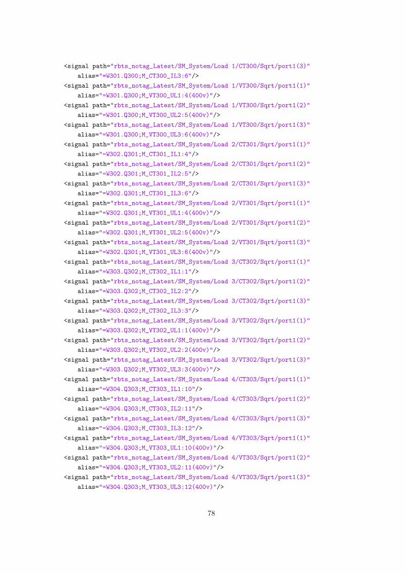
<signal path="rbts_notag_Latest/SM_System/Load 1/CT300/Sqrt/port1(3)"alias="=W301.Q300;M_CT300_IL3:6"/>
<signal path="rbts_notag_Latest/SM_System/Load 1/VT300/Sqrt/port1(1)"alias="=W301.Q300;M_VT300_UL1:4(400v)"/>
<signal path="rbts_notag_Latest/SM_System/Load 1/VT300/Sqrt/port1(2)"alias="=W301.Q300;M_VT300_UL2:5(400v)"/>
<signal path="rbts_notag_Latest/SM_System/Load 1/VT300/Sqrt/port1(3)"alias="=W301.Q300;M_VT300_UL3:6(400v)"/>
<signal path="rbts_notag_Latest/SM_System/Load 2/CT301/Sqrt/port1(1)"alias="=W302.Q301;M_CT301_IL1:4"/>
<signal path="rbts_notag_Latest/SM_System/Load 2/CT301/Sqrt/port1(2)"alias="=W302.Q301;M_CT301_IL2:5"/>
<signal path="rbts_notag_Latest/SM_System/Load 2/CT301/Sqrt/port1(3)"alias="=W302.Q301;M_CT301_IL3:6"/>
<signal path="rbts_notag_Latest/SM_System/Load 2/VT301/Sqrt/port1(1)"alias="=W302.Q301;M_VT301_UL1:4(400v)"/>
<signal path="rbts_notag_Latest/SM_System/Load 2/VT301/Sqrt/port1(2)"alias="=W302.Q301;M_VT301_UL2:5(400v)"/>
<signal path="rbts_notag_Latest/SM_System/Load 2/VT301/Sqrt/port1(3)"alias="=W302.Q301;M_VT301_UL3:6(400v)"/>
<signal path="rbts_notag_Latest/SM_System/Load 3/CT302/Sqrt/port1(1)"alias="=W303.Q302;M_CT302_IL1:1"/>
<signal path="rbts_notag_Latest/SM_System/Load 3/CT302/Sqrt/port1(2)"alias="=W303.Q302;M_CT302_IL2:2"/>
<signal path="rbts_notag_Latest/SM_System/Load 3/CT302/Sqrt/port1(3)"alias="=W303.Q302;M_CT302_IL3:3"/>
<signal path="rbts_notag_Latest/SM_System/Load 3/VT302/Sqrt/port1(1)"alias="=W303.Q302;M_VT302_UL1:1(400v)"/>
<signal path="rbts_notag_Latest/SM_System/Load 3/VT302/Sqrt/port1(2)"alias="=W303.Q302;M_VT302_UL2:2(400v)"/>
<signal path="rbts_notag_Latest/SM_System/Load 3/VT302/Sqrt/port1(3)"alias="=W303.Q302;M_VT302_UL3:3(400v)"/>
<signal path="rbts_notag_Latest/SM_System/Load 4/CT303/Sqrt/port1(1)"alias="=W304.Q303;M_CT303_IL1:10"/>
<signal path="rbts_notag_Latest/SM_System/Load 4/CT303/Sqrt/port1(2)"alias="=W304.Q303;M_CT303_IL2:11"/>
<signal path="rbts_notag_Latest/SM_System/Load 4/CT303/Sqrt/port1(3)"alias="=W304.Q303;M_CT303_IL3:12"/>
<signal path="rbts_notag_Latest/SM_System/Load 4/VT303/Sqrt/port1(1)"alias="=W304.Q303;M_VT303_UL1:10(400v)"/>
<signal path="rbts_notag_Latest/SM_System/Load 4/VT303/Sqrt/port1(2)"alias="=W304.Q303;M_VT303_UL2:11(400v)"/>
<signal path="rbts_notag_Latest/SM_System/Load 4/VT303/Sqrt/port1(3)"alias="=W304.Q303;M_VT303_UL3:12(400v)"/>
78

<signal path="rbts_notag_Latest/SM_System/=W6;/CT407/Sqrt/port1(1)"alias="=W6.Q407;M_CT407_IL1:10"/>
<signal path="rbts_notag_Latest/SM_System/=W6;/CT407/Sqrt/port1(2)"alias="=W6.Q407;M_CT407_IL2:11"/>
<signal path="rbts_notag_Latest/SM_System/=W6;/CT407/Sqrt/port1(3)"alias="=W6.Q407;M_CT407_IL3:12"/>
<signal path="rbts_notag_Latest/SM_System/=W6;/VT407/Sqrt/port1(1)"alias="=W6.Q407;M_VT407_UL1:10(WGEN_1500000W)"/>
<signal path="rbts_notag_Latest/SM_System/=W6;/VT407/Sqrt/port1(2)"alias="=W6.Q407;M_VT407_UL2:11(WGEN_1500000W)"/>
<signal path="rbts_notag_Latest/SM_System/=W6;/VT407/Sqrt/port1(3)"alias="=W6.Q407;M_VT407_UL3:12(WGEN_1500000W)"/><signal path="rbts_notag_Latest/SM_System/=W40;/CT402/Sqrt/port1(1)"
alias="=W40.Q402;M_CT402_IL1:7"/><signal path="rbts_notag_Latest/SM_System/=W40;/CT402/Sqrt/port1(2)"
alias="=W40.Q402;M_CT402_IL2:8"/><signal path="rbts_notag_Latest/SM_System/=W40;/CT402/Sqrt/port1(3)"
alias="=W40.Q402;M_CT402_IL3:9"/><signal path="rbts_notag_Latest/SM_System/=W40;/VT402/Sqrt/port1(1)"
alias="=W40.Q402;M_VT402_UL1:7(WGEN_2000000W)"/><signal path="rbts_notag_Latest/SM_System/=W40;/VT402/Sqrt/port1(2)"
alias="=W40.Q402;M_VT402_UL2:8(WGEN_2000000W)"/><signal path="rbts_notag_Latest/SM_System/=W40;/VT402/Sqrt/port1(3)"
alias="=W40.Q402;M_VT402_UL3:9(WGEN_2000000W)"/><signal path="rbts_notag_Latest/SM_System/=W24;/CT401/Sqrt/port1(1)"
alias="=W24.Q401;M_CT401_IL1:13"/><signal path="rbts_notag_Latest/SM_System/=W24;/CT401/Sqrt/port1(2)"
alias="=W24.Q401;M_CT401_IL2:14"/><signal path="rbts_notag_Latest/SM_System/=W24;/CT401/Sqrt/port1(3)"
alias="=W24.Q401;M_CT401_IL3:15"/><signal path="rbts_notag_Latest/SM_System/=W24;/VT401/Sqrt/port1(1)"
alias="=W24.Q401;M_VT401_UL1:13(WGEN_2000000W)"/><signal path="rbts_notag_Latest/SM_System/=W24;/VT401/Sqrt/port1(2)"
alias="=W24.Q401;M_VT401_UL2:14(WGEN_2000000W)"/><signal path="rbts_notag_Latest/SM_System/=W24;/VT401/Sqrt/port1(3)"
alias="=W24.Q401;M_VT401_UL3:15(WGEN_2000000W)"/><signal path="rbts_notag_Latest/SM_System/=W61;/CT406/Sqrt/port1(1)"
alias="=W61.Q406;M_CT406_IL1:4"/><signal path="rbts_notag_Latest/SM_System/=W61;/CT406/Sqrt/port1(2)"
alias="=W61.Q406;M_CT406_IL2:5"/><signal path="rbts_notag_Latest/SM_System/=W61;/CT406/Sqrt/port1(3)"
alias="=W61.Q406;M_CT406_IL3:6"/><signal path="rbts_notag_Latest/SM_System/=W61;/VT406/Sqrt/port1(1)"
alias="=W61.Q406;M_VT406_UL1:4(WGEN_1500000W)"/>
79
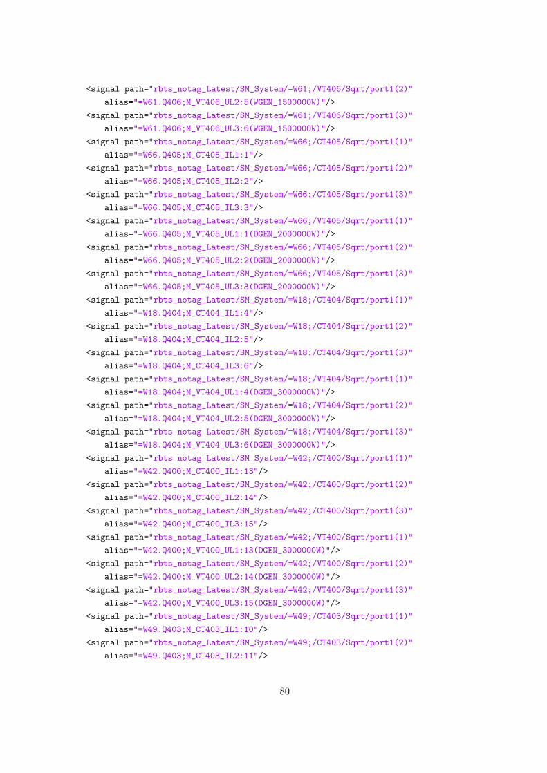
<signal path="rbts_notag_Latest/SM_System/=W61;/VT406/Sqrt/port1(2)"alias="=W61.Q406;M_VT406_UL2:5(WGEN_1500000W)"/>
<signal path="rbts_notag_Latest/SM_System/=W61;/VT406/Sqrt/port1(3)"alias="=W61.Q406;M_VT406_UL3:6(WGEN_1500000W)"/>
<signal path="rbts_notag_Latest/SM_System/=W66;/CT405/Sqrt/port1(1)"alias="=W66.Q405;M_CT405_IL1:1"/>
<signal path="rbts_notag_Latest/SM_System/=W66;/CT405/Sqrt/port1(2)"alias="=W66.Q405;M_CT405_IL2:2"/>
<signal path="rbts_notag_Latest/SM_System/=W66;/CT405/Sqrt/port1(3)"alias="=W66.Q405;M_CT405_IL3:3"/>
<signal path="rbts_notag_Latest/SM_System/=W66;/VT405/Sqrt/port1(1)"alias="=W66.Q405;M_VT405_UL1:1(DGEN_2000000W)"/>
<signal path="rbts_notag_Latest/SM_System/=W66;/VT405/Sqrt/port1(2)"alias="=W66.Q405;M_VT405_UL2:2(DGEN_2000000W)"/>
<signal path="rbts_notag_Latest/SM_System/=W66;/VT405/Sqrt/port1(3)"alias="=W66.Q405;M_VT405_UL3:3(DGEN_2000000W)"/>
<signal path="rbts_notag_Latest/SM_System/=W18;/CT404/Sqrt/port1(1)"alias="=W18.Q404;M_CT404_IL1:4"/>
<signal path="rbts_notag_Latest/SM_System/=W18;/CT404/Sqrt/port1(2)"alias="=W18.Q404;M_CT404_IL2:5"/>
<signal path="rbts_notag_Latest/SM_System/=W18;/CT404/Sqrt/port1(3)"alias="=W18.Q404;M_CT404_IL3:6"/>
<signal path="rbts_notag_Latest/SM_System/=W18;/VT404/Sqrt/port1(1)"alias="=W18.Q404;M_VT404_UL1:4(DGEN_3000000W)"/>
<signal path="rbts_notag_Latest/SM_System/=W18;/VT404/Sqrt/port1(2)"alias="=W18.Q404;M_VT404_UL2:5(DGEN_3000000W)"/>
<signal path="rbts_notag_Latest/SM_System/=W18;/VT404/Sqrt/port1(3)"alias="=W18.Q404;M_VT404_UL3:6(DGEN_3000000W)"/>
<signal path="rbts_notag_Latest/SM_System/=W42;/CT400/Sqrt/port1(1)"alias="=W42.Q400;M_CT400_IL1:13"/>
<signal path="rbts_notag_Latest/SM_System/=W42;/CT400/Sqrt/port1(2)"alias="=W42.Q400;M_CT400_IL2:14"/>
<signal path="rbts_notag_Latest/SM_System/=W42;/CT400/Sqrt/port1(3)"alias="=W42.Q400;M_CT400_IL3:15"/>
<signal path="rbts_notag_Latest/SM_System/=W42;/VT400/Sqrt/port1(1)"alias="=W42.Q400;M_VT400_UL1:13(DGEN_3000000W)"/>
<signal path="rbts_notag_Latest/SM_System/=W42;/VT400/Sqrt/port1(2)"alias="=W42.Q400;M_VT400_UL2:14(DGEN_3000000W)"/>
<signal path="rbts_notag_Latest/SM_System/=W42;/VT400/Sqrt/port1(3)"alias="=W42.Q400;M_VT400_UL3:15(DGEN_3000000W)"/>
<signal path="rbts_notag_Latest/SM_System/=W49;/CT403/Sqrt/port1(1)"alias="=W49.Q403;M_CT403_IL1:10"/>
<signal path="rbts_notag_Latest/SM_System/=W49;/CT403/Sqrt/port1(2)"alias="=W49.Q403;M_CT403_IL2:11"/>
80

<signal path="rbts_notag_Latest/SM_System/=W49;/CT403/Sqrt/port1(3)"alias="=W49.Q403;M_CT403_IL3:12"/>
<signal path="rbts_notag_Latest/SM_System/=W49;/VT403/Sqrt/port1(1)"alias="=W49.Q403;M_VT403_UL1:10(DGEN_2000000W)"/><signal path="rbts_notag_Latest/SM_System/=W49;/VT403/Sqrt/port1(2)"
alias="=W49.Q403;M_VT403_UL2:11(DGEN_2000000W)"/><signal path="rbts_notag_Latest/SM_System/=W49;/VT403/Sqrt/port1(3)"
alias="=W49.Q403;M_VT403_UL3:12(DGEN_2000000W)"/>
</signals>
</root>
81