eval6470h, eval6470pd, eval6472h and … · user manual eval6470h, eval6470pd, eval6472h and...
TRANSCRIPT

April 2015 DocID025471 Rev 2 1/41
41
UM1688User manual
EVAL6470H, EVAL6470PD, EVAL6472H and EVAL6472PD: fullyintegrated microstepping motor drivers
Introduction
The EVAL6470H, EVAL6470PD, EVAL6472H and EVAL6472PD are four demonstration boards based on the L6470 and L6472 devices implementing a complete stepper motor driver solution. They are designed for operate with a supply voltage ranging from 8 V to 45 V and can drive up to 3 Ar.m.s. for each phase.
In combination with the STEVAL-PCC009V2 demonstration board and the SPINFamily evaluation tool, the boards provide a complete and easy to use evaluation environment allowing the user to investigate all the features of the L6470 and L6472 devices. Both the boards support the daisy chain configuration making them suitable for the evaluation of the devices in multi motor applications.
www.st.com
Contents UM1688
2/41 DocID025471 Rev 2
Contents
1 Boards description . . . . . . . . . . . . . . . . . . . . . . . . . . . . . . . . . . . . . . . . . . 5
1.1 EVAL6470H . . . . . . . . . . . . . . . . . . . . . . . . . . . . . . . . . . . . . . . . . . . . . . . . 5
EVAL6470H - thermal data . . . . . . . . . . . . . . . . . . . . . . . . . . . . . . . . . . . . . . . . . . 12
1.2 EVAL6470PD . . . . . . . . . . . . . . . . . . . . . . . . . . . . . . . . . . . . . . . . . . . . . . 12
EVAL6470PD - thermal data. . . . . . . . . . . . . . . . . . . . . . . . . . . . . . . . . . . . . . . . . 20
1.3 EVAL6472H . . . . . . . . . . . . . . . . . . . . . . . . . . . . . . . . . . . . . . . . . . . . . . . 21
EVAL6472H - thermal data . . . . . . . . . . . . . . . . . . . . . . . . . . . . . . . . . . . . . . . . . . 28
1.4 EVAL6472PD . . . . . . . . . . . . . . . . . . . . . . . . . . . . . . . . . . . . . . . . . . . . . . 28
EVAL6472PD - thermal data. . . . . . . . . . . . . . . . . . . . . . . . . . . . . . . . . . . . . . . . . 34
2 Evaluation environment setup . . . . . . . . . . . . . . . . . . . . . . . . . . . . . . . . 35
3 Device configuration . . . . . . . . . . . . . . . . . . . . . . . . . . . . . . . . . . . . . . . . 36
3.1 Voltage mode driving (EVAL6470H/PD) . . . . . . . . . . . . . . . . . . . . . . . . . . 36
3.2 Advanced current control (EVAL6472H/PD) . . . . . . . . . . . . . . . . . . . . . . 37
3.3 Overcurrent and stall detection thresholds . . . . . . . . . . . . . . . . . . . . . . . . 37
3.4 Speed profile . . . . . . . . . . . . . . . . . . . . . . . . . . . . . . . . . . . . . . . . . . . . . . 37
4 How to change the supply configuration of the board . . . . . . . . . . . . 39
5 Daisy chaining . . . . . . . . . . . . . . . . . . . . . . . . . . . . . . . . . . . . . . . . . . . . . 40
6 Revision history . . . . . . . . . . . . . . . . . . . . . . . . . . . . . . . . . . . . . . . . . . . 40

DocID025471 Rev 2 3/41
UM1688 List of tables
41
List of tables
Table 1. EVAL6470H - specifications . . . . . . . . . . . . . . . . . . . . . . . . . . . . . . . . . . . . . . . . . . . . . . . . . 5Table 2. EVAL6470H - jumpers and connectors description . . . . . . . . . . . . . . . . . . . . . . . . . . . . . . . 6Table 3. EVAL6470H - master SPI connector pinout (J10) . . . . . . . . . . . . . . . . . . . . . . . . . . . . . . . . 6Table 4. EVAL6470H - slave SPI connector pinout (J11) . . . . . . . . . . . . . . . . . . . . . . . . . . . . . . . . . . 7Table 5. EVAL6470H - bill of material. . . . . . . . . . . . . . . . . . . . . . . . . . . . . . . . . . . . . . . . . . . . . . . . . 9Table 6. EVAL6470PD - specifications. . . . . . . . . . . . . . . . . . . . . . . . . . . . . . . . . . . . . . . . . . . . . . . 12Table 7. EVAL6470PD - jumper and connector description . . . . . . . . . . . . . . . . . . . . . . . . . . . . . . . 14Table 8. EVAL6470PD - master SPI connector pinout (J10) . . . . . . . . . . . . . . . . . . . . . . . . . . . . . . 14Table 9. EVAL6470PD - slave SPI connector pinout (J11) . . . . . . . . . . . . . . . . . . . . . . . . . . . . . . . 15Table 10. EVAL6470PD - bill of material . . . . . . . . . . . . . . . . . . . . . . . . . . . . . . . . . . . . . . . . . . . . . . 17Table 11. EVAL6472H - specifications . . . . . . . . . . . . . . . . . . . . . . . . . . . . . . . . . . . . . . . . . . . . . . . . 21Table 12. EVAL6472H - jumpers and connectors description . . . . . . . . . . . . . . . . . . . . . . . . . . . . . . 22Table 13. EVAL6472H - master SPI connector pinout (J10) . . . . . . . . . . . . . . . . . . . . . . . . . . . . . . . 22Table 14. EVAL6472H - slave SPI connector pinout (J11) . . . . . . . . . . . . . . . . . . . . . . . . . . . . . . . . . 23Table 15. EVAL6472H - bill of material. . . . . . . . . . . . . . . . . . . . . . . . . . . . . . . . . . . . . . . . . . . . . . . . 25Table 16. EVAL6472PD - specifications. . . . . . . . . . . . . . . . . . . . . . . . . . . . . . . . . . . . . . . . . . . . . . . 28Table 17. EVAL6472PD - jumper and connector description . . . . . . . . . . . . . . . . . . . . . . . . . . . . . . . 29Table 18. EVAL6472PD - master SPI connector pinout (J10) . . . . . . . . . . . . . . . . . . . . . . . . . . . . . . 30Table 19. EVAL6472PD - slave SPI connector pinout (J11) . . . . . . . . . . . . . . . . . . . . . . . . . . . . . . . 30Table 20. EVAL6472PD - bill of material . . . . . . . . . . . . . . . . . . . . . . . . . . . . . . . . . . . . . . . . . . . . . . 32Table 21. Device supply configurations . . . . . . . . . . . . . . . . . . . . . . . . . . . . . . . . . . . . . . . . . . . . . . . 39Table 22. Document revision history . . . . . . . . . . . . . . . . . . . . . . . . . . . . . . . . . . . . . . . . . . . . . . . . . 40

List of figures UM1688
4/41 DocID025471 Rev 2
List of figures
Figure 1. EVAL6470H - jumpers and connectors location . . . . . . . . . . . . . . . . . . . . . . . . . . . . . . . . . . 5Figure 2. EVAL6470H - schematic. . . . . . . . . . . . . . . . . . . . . . . . . . . . . . . . . . . . . . . . . . . . . . . . . . . . 8Figure 3. EVAL6470H - layout (top layer) . . . . . . . . . . . . . . . . . . . . . . . . . . . . . . . . . . . . . . . . . . . . . 10Figure 4. EVAL6470H - layout (inner layer 2) . . . . . . . . . . . . . . . . . . . . . . . . . . . . . . . . . . . . . . . . . . 10Figure 5. EVAL6470H - layout (inner layer 3) . . . . . . . . . . . . . . . . . . . . . . . . . . . . . . . . . . . . . . . . . . 11Figure 6. EVAL6470H - layout (bottom layer) . . . . . . . . . . . . . . . . . . . . . . . . . . . . . . . . . . . . . . . . . . 11Figure 7. EVAL6470H - thermal impedance graph . . . . . . . . . . . . . . . . . . . . . . . . . . . . . . . . . . . . . . 12Figure 8. EVAL6470PD - jumper and connector location . . . . . . . . . . . . . . . . . . . . . . . . . . . . . . . . . 13Figure 9. EVAL6470PD - schematic . . . . . . . . . . . . . . . . . . . . . . . . . . . . . . . . . . . . . . . . . . . . . . . . . 16Figure 10. EVAL6470PD - layout (top layer) . . . . . . . . . . . . . . . . . . . . . . . . . . . . . . . . . . . . . . . . . . . . 18Figure 11. EVAL6470PD - layout (inner layer 2) . . . . . . . . . . . . . . . . . . . . . . . . . . . . . . . . . . . . . . . . . 18Figure 12. EVAL6470PD - layout (inner layer 3) . . . . . . . . . . . . . . . . . . . . . . . . . . . . . . . . . . . . . . . . . 19Figure 13. EVAL6470PD - layout (bottom layer . . . . . . . . . . . . . . . . . . . . . . . . . . . . . . . . . . . . . . . . . . 19Figure 14. EVAL6470PD - thermal impedance graph . . . . . . . . . . . . . . . . . . . . . . . . . . . . . . . . . . . . . 20Figure 15. EVAL6472H - jumpers and connectors location . . . . . . . . . . . . . . . . . . . . . . . . . . . . . . . . . 21Figure 16. EVAL6472H - schematic. . . . . . . . . . . . . . . . . . . . . . . . . . . . . . . . . . . . . . . . . . . . . . . . . . . 24Figure 17. EVAL6472H - layout (top layer) . . . . . . . . . . . . . . . . . . . . . . . . . . . . . . . . . . . . . . . . . . . . . 26Figure 18. EVAL6472H - layout (inner layer2) . . . . . . . . . . . . . . . . . . . . . . . . . . . . . . . . . . . . . . . . . . . 26Figure 19. EVAL6472H - layout (inner layer3) . . . . . . . . . . . . . . . . . . . . . . . . . . . . . . . . . . . . . . . . . . . 27Figure 20. EVAL6472H - layout (bottom layer3) . . . . . . . . . . . . . . . . . . . . . . . . . . . . . . . . . . . . . . . . . 27Figure 21. EVAL6472H - thermal impedance graph . . . . . . . . . . . . . . . . . . . . . . . . . . . . . . . . . . . . . . 28Figure 22. EVAL6472PD - jumper and connector location . . . . . . . . . . . . . . . . . . . . . . . . . . . . . . . . . 29Figure 23. EVAL6472PD - schematic . . . . . . . . . . . . . . . . . . . . . . . . . . . . . . . . . . . . . . . . . . . . . . . . . 31Figure 24. EVAL6472PD - layout (inner layer2). . . . . . . . . . . . . . . . . . . . . . . . . . . . . . . . . . . . . . . . . . 33Figure 25. EVAL6472PD - layout (inner layer3). . . . . . . . . . . . . . . . . . . . . . . . . . . . . . . . . . . . . . . . . . 33Figure 26. EVAL6472PD - layout (bottom layer3) . . . . . . . . . . . . . . . . . . . . . . . . . . . . . . . . . . . . . . . . 34Figure 27. EVAL6472PD - thermal impedance graph . . . . . . . . . . . . . . . . . . . . . . . . . . . . . . . . . . . . . 34

DocID025471 Rev 2 5/41
UM1688 Boards description
41
1 Boards description
1.1 EVAL6470H
Figure 1. EVAL6470H - jumpers and connectors location
Table 1. EVAL6470H - specifications
Parameter Value
Supply voltage (VS) 8 to 45 V
Maximum output current (each phase) 3 Ar.m.s.
Logic supply voltage (VREG)Externally supplied: 3.3 V, internally supplied: 3 V
(typ.)
Logic interface voltage (VDD)Externally supplied: 3.3 V or 5 V, internally
supplied: VREG
Low level logic inputs voltage 0 V
High level logic input voltage VDD(1)
1. All logic inputs are 5 V tolerant.
Operating temperature -25 to +125 °C
L6470H thermal resistance junction to ambient 21 °C/W (typ.)

Boards description UM1688
6/41 DocID025471 Rev 2
Table 2. EVAL6470H - jumpers and connectors description
Name Type Function
J1 Power supply Motor supply voltage
J5 Power output Bridge A outputs
J6 Power output Bridge B outputs
J2 SPI connector Master SPI
J3 SPI connector Slave SPI
J4 NM connector OSCIN and OSCOUT pins
J7 NM connector External switch input
TP1 (VS) Test point Motor supply voltage test point
TP4 (VDD) Test point Logic interface supply voltage test point
TP5 (VREG) Test point Logic supply voltage/L6470 internal regulator test point
TP6 (GND) Test point Ground test point
TP2 (STCK) Test point Step-clock input test point
TP3 (STBY/RES) Test point Standby/reset input test point
TP7 (FLAG) Test point FLAG output test point
TP8 (BUSY/SYNC) Test point BUSY/SYNC output test point
Table 3. EVAL6470H - master SPI connector pinout (J10)
Pin number Type Description
1 Open drain output L6470 BUSY/SYNC output
2 Open drain output L6470 FLAG output
3 Ground Ground
4 Supply EXT_VDD (can be used as external logic power supply)
5 Digital outputSPI master IN slave OUT signal (connected to L6470 SDO
output through daisy-chain termination jumper JP2)
6 Digital input SPI serial clock signal (connected to L6470 CK input)
7 Digital inputSPI master OUT slave IN signal (connected to L6470 SDI
input)
8 Digital input SPI slave select signal (connected to L6470 CS input)
9 Digital input L6470 step-clock input
10 Digital input L6470 STBY/RST input

DocID025471 Rev 2 7/41
UM1688 Boards description
41
Table 4. EVAL6470H - slave SPI connector pinout (J11)
Pin number Type Description
1 Open drain output L6470 BUSY/SYNC output
2 Open drain output L6470 FLAG output
3 Ground Ground
4 Supply EXT_VDD (can be used as external logic power supply)
5 Digital output SPI master IN slave OUT signal (connected to pin 5 of J10)
6 Digital input SPI serial clock signal (connected to L6470 CK input)
7 Digital inputSPI master OUT slave IN signal (connected to L6470 SDO
output)
8 Digital input SPI slave select signal (connected to L6470 CS input)
9 Digital input L6470 step-clock input
10 Digital input L6470 STBY/RST input

Boards description UM1688
8/41 DocID025471 Rev 2
Figure 2. EVAL6470H - schematic

DocID025471 Rev 2 9/41
UM1688 Boards description
41
Table 5. EVAL6470H - bill of material
Item Quantity Reference Value Package
1 1 C1 220 nF/16 V CAPC-0603
2 2 C2,C4 100 nF/6.3 V CAPC-0603
3 1 C3 10 µF/6.3 V CAPC-3216
4 1 C5 47 µF/6.3 V CAPC-3216
5 1 C6 10 nF/50 V CAPC-0603
6 4 C7, C8, C15, C16 100 nF/50 V CAPC-0603
7 1 C9A 100 µF/63 V CAPE-R8H12-P35
8 1 C9 100 µF/63 V CAPES-R10HXX
9 3 C10, C11, C12 100 pF/6.3 V CAPC-0603
10 1 C13 3.3 nF/6.3 V CAPC-0603
11 1 C14 10 nF/6.3 V CAPC-0603
12 1 DL1 LED diode (red) LEDC-0805
13 1 DL2 LED diode (amber) LEDC-0805
14 1 D1 BAV99 SOT23
15 1 D2 BZX585-B3V6(1) SOD523
16 1 JP1 Jumper - OPEN JP2SO
17 2 JP2, JP3 Jumper - CLOSED JP2SO
18 3 J1, J5, J6 Screw connector 2 poles MORSV-508-2P
19 2 J2,J3Pol. IDC male header vertical 10
polesCON-FLAT-5X2-180M
20 2 J4,J7 N.M. STRIP254P-M-2
21 1 R1 31.6 k RESC-0603
22 1 R2 200 kTRIMM-100X50X110-
64W
23 1 R3 8.2 k RESC-0603
24 3 R4, R5, R6 39 k RESC-0603
25 2 R7, R9 470 RESC-0603
26 1 R8 100 RESC-0603
27 8TP1, TP2, TP3, TP4, TP5,
TP6, TP7, TP8Test point TH
28 1 U1 L6470 HTSSOP28

Boards description UM1688
10/41 DocID025471 Rev 2
Figure 3. EVAL6470H - layout (top layer)
Figure 4. EVAL6470H - layout (inner layer 2)

DocID025471 Rev 2 11/41
UM1688 Boards description
41
Figure 6. EVAL6470H - layout (bottom layer)
Figure 5. EVAL6470H - layout (inner layer 3)

Boards description UM1688
12/41 DocID025471 Rev 2
EVAL6470H - thermal data
Figure 7. EVAL6470H - thermal impedance graph
1.2 EVAL6470PD
20
25
15
10
5
01 10 100 1000
Time(seconds)
Zth(
°C/W
)
Zth
AM11339v1
Table 6. EVAL6470PD - specifications
Parameter Value
Supply voltage (VS) 8 to 45 V
Maximum output current (each phase) 3 Ar.m.s.
Logic supply voltage (VREG) Externally supplied: 3.3 V internally supplied: 3 V typical
Logic interface voltage (VDD) Externally supplied: 3.3 V or 5 V internally supplied: VREG
Low level logic input voltage 0 V
High level logic input voltage VDD(1)
Operating temperature -25 to +125 °C
L6470PD thermal resistance junction to ambient 12 °C/W typical
1. All logic inputs are 5 V tolerant.

DocID025471 Rev 2 13/41
UM1688 Boards description
41
Figure 8. EVAL6470PD - jumper and connector location
AM11330v1

Boards description UM1688
14/41 DocID025471 Rev 2
Table 7. EVAL6470PD - jumper and connector description
Name Type Function
M1 Power supply Motor supply voltage
M2 Power output Bridge A outputs
M3 Power output Bridge B outputs
CN1 SPI connector Master SPI
CN2 SPI connector Slave SPI
CN3 NM connector OSCIN and OSCOUT pins
CN4 NM connector External switch input
TP1 (VS) Test point Motor supply voltage test point
TP2 (VDD) Test point Logic interface supply voltage test point
TP3 (VREG) Test point Logic supply voltage/L6470 internal regulator test point
TP5 (GND) Test point Ground test point
TP6 (GND) Test point Ground test point
TP8 (STCK) Test point Step-clock input test point
TP9 (STBY/RES) Test point Standby/reset input test point
TP10 (FLAG) Test point FLAG output test point
TP11 (BUSY/SYNC) Test point BUSY/SYNC output test point
Table 8. EVAL6470PD - master SPI connector pinout (J10)
Pin number Type Description
1 Open drain output L6470 BUSY/SYNC output
2 Open drain output L6470 FLAG output
3 Ground Ground
4 Supply EXT_VDD (can be used as external logic power supply)
5 Digital outputSPI master IN slave OUT signal (connected to the L6470 SDO
output through the daisy chain termination jumper JP2)
6 Digital input SPI serial clock signal (connected to L6470 CK input)
7 Digital input SPI master OUT slave IN signal (connected to L6470 SDI input)
8 Digital input SPI slave select signal (connected to L6470 CS input)
9 Digital input L6470 step-clock input
10 Digital input L6470 STBY/RST input

DocID025471 Rev 2 15/41
UM1688 Boards description
41
Table 9. EVAL6470PD - slave SPI connector pinout (J11)
Pin number Type Description
1 Open drain output L6470 BUSY/SYNC output
2 Open drain output L6470 FLAG output
3 Ground Ground
4 Supply EXT_VDD (can be used as external logic power supply)
5 Digital output SPI master IN slave OUT signal (connected to pin 5 of J10)
6 Digital input SPI serial clock signal (connected to L6470 CK input)
7 Digital input SPI master OUT slave IN signal (connected to L6470 SDO output)
8 Digital input SPI slave select signal (connected to L6470 CS input)
9 Digital input L6470 step-clock input
10 Digital input L6470 STBY/RST input

Boards description UM1688
16/41 DocID025471 Rev 2
Figure 9. EVAL6470PD - schematic
1A 2A
SW
1B 2B
OS
CIN
OS
CO
UT
App
licat
ion
refe
renc
e
VS
GN
D
GERVDDV
SP
I_IN
SP
I_O
UT
YSUBGAL F
OP
TIO
N
YBT SKC TS
VS
GN
DG
ND
SW
MIS
OS
DI
CK
nCS
FLA
GB
US
Y
ST
CK
ST
BY
_RE
SE
T
MIS
OS
DO
CK
nCS
FLA
GB
US
Y
SD
OM
ISO
BU
SY
SD
IC
KnC
S
SW
ST
CK
AD
CIN
SD
O
FLA
GB
US
Y
FLA
GS
TB
Y_R
ES
ET
ST
CK
ST
BY
_RE
SE
T
VS
VS
EX
T_V
DD
EX
T_V
DD
EX
T_V
DD
VD
D
VR
EG
VR
EG
VD
D
VR
EG
VD
D
VD
D
VD
DV
DD
VS
VS
TP
1
1
C1510
0nF
/50V
CN
3N
.M.
12
CN
11
23
45
67
89
10
C9
100p
F/6
.3V
R4
39K
M2
1 2
C3
10nF
/50V
+C
1
100u
F/6
3VJP3
U1
L647
0
VDD24
VREG9
OS
CIN
10
OS
CO
UT
11
CP13
VBOOT14
AD
CIN
8
VSA4
VSA5
VSB15
VSB16 PGND
1
OU
T1A
2
OU
T2A
35
OU
T1B
17
OU
T2B
20
AGND12
SW
7
DGND
28
BU
SY
_SY
NC
29F
LAG
31
SD
O25
SD
I27
CK
26C
S30
ST
BY
_RE
S6
ST
CK
32
OU
T1A
3
OU
T1B
18
OU
T2B
21
OU
T2A
36
VSB22
VSB23
VSA
33
VSA34
PGND19
E_PAD
37
TP
6
1
C13
10nF
/6.3
V
TP
11
1
TP
10
1
C11
1nF
/6.3
V
R6
470
C8
220n
F/1
6V
R8
10K
C2
100n
F/5
0V
C6
100n
F/6
.3V
TP
21
CN
4 N.M
.1 2D
L1
21
TR
120
0k
13
2
C16 10
0nF
/50V
DL2
21
M3
12
R3
39K
R1
31K
6
C12
3.3n
F/6
.3V
TP
9
1
TP
31
D2
BZ
X58
5-B
3V6
+C
1A10
0uF
/63V
R5
39K
C5
47uF
/6.3
V
CN
21
23
45
67
89
10
R7
470
TP
5
1
M1
1 2
C4
100n
F/6
.3V
TP
8
1
JP2
C10
100p
F/6
.3V
D1
BA
V99
12
3
C14
100n
F/5
0V
R2
8K
2
C7
10uF
/6.3
V
JP1
AM12921v1

DocID025471 Rev 2 17/41
UM1688 Boards description
41
Table 10. EVAL6470PD - bill of material
Index Quantity Reference Value Package
1 1 CN1Pol. IDC male header vertical 10 poles
(black)CON-FLAT-5X2-180M
2 1 CN2Pol. IDC male header vertical 10 poles
(gray)CON-FLAT-5X2-180M
3 2 CN3, CN4 N. M. STRIP254P-M-2
4 1 C1A 100 µF/63 V (option) CAPE-R10HXX-P5
5 1 C1 100 µF/63 V CAPES-R10HXX
6 4 C2, C14, C15, C1 100 nF/50 V CAPC-0603
7 1 C3 10 nF/50 V CAPC-0603
8 2 C4, C6 100 nF/6.3 V CAPC-0603
9 1 C5 47 µF/6.3 V CAPC-1206
10 1 C7 10 µF/6.3 V CAPC-0805
11 1 C8 220 nF/16 V CAPC-0603
12 2 C9, C10 100 pF/6.3 V CAPC-0603
13 1 C11 1 nF/6.3 V CAPC-0603
14 1 C12 3.3 nF/6.3 V CAPC-0603
15 1 C13 10 nF/6.3 V CAPC-0603
16 1 DL1 LED red LEDC-0805
17 1 DL2 LED amber LEDC-0805
18 1 D1 BAV99 SOT23
19 1 D2 BZX585-B3V6 SOD523
20 1 JP1 Jumper OPEN JP2SO
21 2 JP2, JP3 Jumper CLOSED JP2SO
22 3 M1, M2, M3 Screw connector 2 poles MORSV-508-2P
23 1 R1 31.6 k RESC-0603
24 1 R2 8.2 k RESC-0603
25 3 R3, R4, R5 39 k RESC-0603
26 2 R6, R7 470 k RESC-0603
27 1 R8 10 k RESC-0603
28 9TP1, TP2, TP3, TP5, TP6,
TP8, TP9, TP10, TP11TPTH-RING-1MM TH
29 1 TR1 200 k TRIMM-100x50x110-64W
30 1 U1 L6470 PowerSO36

Boards description UM1688
18/41 DocID025471 Rev 2
Figure 11. EVAL6470PD - layout (inner layer 2)
Figure 10. EVAL6470PD - layout (top layer)
AM12923v1
AM12924v1

DocID025471 Rev 2 19/41
UM1688 Boards description
41
Figure 12. EVAL6470PD - layout (inner layer 3)
Figure 13. EVAL6470PD - layout (bottom layer
AM12925v1
AM12926v1

Boards description UM1688
20/41 DocID025471 Rev 2
EVAL6470PD - thermal data
Figure 14. EVAL6470PD - thermal impedance graph
0
2
4
6
8
10
1 10 100 1000 10000
Time (seconds)
Zth
Z
th(°
C/W
)
12
AM11337v1

DocID025471 Rev 2 21/41
UM1688 Boards description
41
1.3 EVAL6472H
Figure 15. EVAL6472H - jumpers and connectors location
Table 11. EVAL6472H - specifications
Parameter Value
Supply voltage (VS) 8 to 45 V
Maximum output current (each phase) 3 Ar.m.s.
Logic supply voltage (VREG)Externally supplied: 3.3 V
Internally supplied: 3 V typical
Logic interface voltage (VDD)Externally supplied: 3.3 V or 5 V
Internally supplied: VREG
Low level logic input voltage 0 V
High level logic input voltage VDD(1)
1. All logic inputs are 5 V tolerant.
Operating temperature -25 to +125 °C
L6472H thermal resistance junction to ambient 21 °C/W typical
Phase A connector
Power supply connector(8 V - 45 V)
Master SPIconnector
BUSY LED(Amber)
FLAG LED(Red)
Motor supply voltagecompensation
partitioning regulation(ADCIN input)
External switch connector(SW input)
JP1: VDD supply frommaster SPI connector
JP2: VDD to VREG connection
OSCIN/OSCOUT connector
JP3: Daisy chain termination
Phase B connector
Slave SPIconnector
Application referencearea
AM10289V1

Boards description UM1688
22/41 DocID025471 Rev 2
Table 12. EVAL6472H - jumpers and connectors description
Name Type Function
M1 Power supply Motor supply voltage
M2 Power output Bridge A outputs
M3 Power output Bridge B outputs
CN1 SPI connector Master SPI
CN2 SPI connector Slave SPI
CN3 NM connector OSCIN and OSCOUT pins
CN4 NM connector External switch input
TP1 (VS) Test point Motor supply voltage test point
TP2 (VDD) Test point Logic interface supply voltage test point
TP3 (VREG) Test point Logic supply voltage/L6470 internal regulator test point
TP5 (GND) Test point Ground test point
TP6 (GND) Test point Ground test point
TP8 (STCK) Test point Step-clock input test point
TP9 (STBY/RES) Test point Standby/reset input test point
TP10 (FLAG) Test point FLAG output test point
TP11 (BUSY/SYNC) Test point BUSY/SYNC output test point
Table 13. EVAL6472H - master SPI connector pinout (J10)
Pin number Type Description
1 Open drain output L6472 BUSY output
2 Open drain output L6472 FLAG output
3 Ground Ground
4 Supply EXT_VDD (can be used as external logic power supply)
5 Digital outputSPI master IN slave OUT signal (connected to L6472 SDO
output through daisy chain termination jumper JP2)
6 Digital input SPI serial clock signal (connected to L6472 CK input)
7 Digital inputSPI master OUT slave IN signal (connected to L6472 SDI
input)
8 Digital input SPI slave select signal (connected to L6472 CS input)
9 Digital input L6472 step-clock input
10 Digital input L6472 standby/reset input
DocID025471 Rev 2 23/41
UM1688 Boards description
41
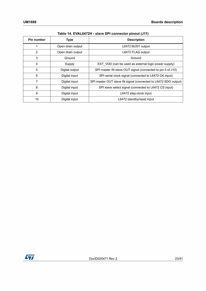
Table 14. EVAL6472H - slave SPI connector pinout (J11)
Pin number Type Description
1 Open drain output L6472 BUSY output
2 Open drain output L6472 FLAG output
3 Ground Ground
4 Supply EXT_VDD (can be used as external logic power supply)
5 Digital output SPI master IN slave OUT signal (connected to pin 5 of J10)
6 Digital input SPI serial clock signal (connected to L6472 CK input)
7 Digital input SPI master OUT slave IN signal (connected to L6472 SDO output)
8 Digital input SPI slave select signal (connected to L6472 CS input)
9 Digital input L6472 step-clock input
10 Digital input L6472 standby/reset input

Boards description UM1688
24/41 DocID025471 Rev 2
Figure 16. EVAL6472H - schematic
1A 2A
SW
1B 2B
OSCI
NOS
COUT
App
licat
ion
refe
renc
e
VS
GN
D
OPTION
SE
R/
YB
TS
KC
TS
TU
O_
IP
SN
I_
IP
S
YS
UB
GA
LF
GNDVDD
VREG
VS
SW
MISO
SDI
CKnCS
FLAG
BUSY
STCK
STBY_RESET
MISO
SDO
CKnCS
FLAG
BUSY
SDO
MISO
BUSY
SDI
CKnCS
SWADCIN
SDO
BUSY
FLAG
FLAG
STBY_RESET
STCK
STCK
STBY_RESET
VS
VS
EXT_VDD
EXT_VDD
EXT_VDD
VDD
VREG
VREG
VDD
VREG
VDD
VS
VDD
VDD
VDD
VS
VS
J6MORSV-508-2P
12
J4 NM
12
C10100pF/6V3
J21
23
45
67
89
10
J1
MORSV-508-2P
1 2
TP1 1
DL2 YELLOW
21
C610nF/50V
D1
BAV99
12
3
JP3
DL1 RED
21
C1
220nF/16V
C15
100nF/50V
R9
470
C12100pF/6V3
TP7 1
TP8 1
C1410nF/6V3
U1
L6472
VDD17VREG6
OSCIN
7
OSCOUT
8
CP10
VBOOT11
ADCIN
5
VSA2VSA26VSB12VSB16
PGND13
PGND27
OUT1A
1
OUT2A
28
OUT1B
14
OUT2B
15
AGND9
SW
4
DGND21
BUSY_SYNC
22FLAG
24
SDO
18SDI
20CK
19CS
23
STBY_RES
3STCK
25
EPAD29
TP4 1C
4100nF/6V3
+C547uF/6V3
C8
100nF/50V
R8100
R2200K
13
2
+C310uF/6V3
R131k6
R539k
R7
470
+C9A100uF/63V
J5 MORSV-508-2P
1 2
TP31
C133.3nF/6V3
D2
BZX585-B3V6
TP5 1
C7
100nF/50V
R639k
TP6 1
J31
23
45
67
89
10
C16
100nF/50V
C11100pF/6V3
JP2
TP21
C2
100nF/6V3
R439k
J7 NM
1 2
R38k2
+C9
100uF/63V
JP1
AM10295V1

DocID025471 Rev 2 25/41
UM1688 Boards description
41
Table 15. EVAL6472H - bill of material
Index Quantity Reference Value Package
1 1 C1 220 nF/16 V CAPC-0603
2 2 C2, C4 100 nF/6.3 V CAPC-0603
3 1 C3 10 µF/6.3 V CAPC-3216
4 1 C5 47 µF/6.3 V CAPC-3216
5 1 C6 10 nF/50 V CAPC-0603
6 4 C7, C8, C15, C16 100 nF/50 V CAPC-0603
7 1 C9A 100 µF/6.3 V (option) CAPE-R10HXX-P5
8 1 C9 100 µF/6.3 V CAPES-R10HXX
9 3 C10, C11, C12 100 pF/6.3 V CAPC-0603
10 1 C13 3.3 nF/6.3 V CAPC-0603
11 1 C14 10 nF/6.3 V CAPC-0603
12 1 DL1 LED diode (red) LEDC-0805
13 1 DL2 LED diode (amber) LEDC-0805
14 1 D1 BAV99 SOT23
15 1 D2 BZX585-B3V6 SOD323
16 1 JP1 Jumper - open JP2SO
17 2 JP2, JP3 Jumper - closed JP2SO
18 3 J1, J5, J6 Screw connector 2 poles MORSV-508-2P
19 2 J2,J3Pol. IDC male header vertical 10
polesCON-FLAT-5X2-180M
20 2 J4, J7 NM STRIP254P-M-2
21 1 R1 31.6 k RESC-0603
22 1 R2 200 k TRIMM-100X50X110-64W
23 1 R3 8.2 k RESC-0603
24 3 R4, R5, R6 39 k RESC-0603
25 2 R7, R9 470 RESC-0603
26 1 R8 100 RESC-0603
27 7TP1, TP2, TP3, TP4,
TP5, TP7, TP8TPTH-ring-1 mm red TH
28 1 TP6 TPTH-ring-1 mm black TH
29 1 U1 L6472 HTSSOP28

Boards description UM1688
26/41 DocID025471 Rev 2
Figure 17. EVAL6472H - layout (top layer)
Figure 18. EVAL6472H - layout (inner layer2)
AM10290V1
AM10291V1

DocID025471 Rev 2 27/41
UM1688 Boards description
41
Figure 19. EVAL6472H - layout (inner layer3)
Figure 20. EVAL6472H - layout (bottom layer3)
AM10292V1
AM10293V1

Boards description UM1688
28/41 DocID025471 Rev 2
EVAL6472H - thermal data
Figure 21. EVAL6472H - thermal impedance graph
1.4 EVAL6472PD
1 10 100 1000
Time (sec)
0
5
10
15
20
25Z
th (
°C/W
)
AM10294V1
Table 16. EVAL6472PD - specifications
Parameter Value
Supply voltage (VS) 8 to 45 V
Maximum output current (each phase) 3 Ar.m.s.
Logic supply voltage (VREG)Externally supplied: 3.3 V
Internally supplied: 3 V typical
Logic interface voltage (VDD)Externally supplied: 3.3 V or 5 V
Internally supplied: VREG
Low level logic input voltage 0 V
High level logic input voltage VDD(1)
1. All logic inputs are 5 V tolerant.
Operating temperature -25 to +125 °C
L6472PD thermal resistance junction to ambient 12 °C/W typical

DocID025471 Rev 2 29/41
UM1688 Boards description
41
Figure 22. EVAL6472PD - jumper and connector location
Table 17. EVAL6472PD - jumper and connector description
Name Type Function
M1 Power supply Motor supply voltage
M2 Power output Bridge A outputs
M3 Power output Bridge B outputs
CN1 SPI connector Master SPI
CN2 SPI connector Slave SPI
CN3 NM connector OSCIN and OSCOUT pins
CN4 NM connector External switch input
TP1 (VS) Test point Motor supply voltage test point
TP2 (VDD) Test point Logic interface supply voltage test point
TP3 (VREG) Test point Logic supply voltage/L6472 internal regulator test point
TP5 (GND) Test point Ground test point
TP6 (GND) Test point Ground test point
TP8 (STCK) Test point Step-clock input test point
TP9 (STBY/RES) Test point Standby/reset input test point
TP10 (FLAG) Test point FLAG output test point
TP11 (BUSY/SYNC) Test point BUSY/SYNC output test point
Phase A connector
Power supply connector(8 V - 45 V)
Master SPIconnector
BUSY LED(Amber)
FLAG LED(Red)
ADCIN input
External switch connector(SW input)
JP1: VDD supply frommaster SPI connector
JP2: VDD to VREG connection
OSCIN/OSCOUT connector
JP3: Daisy chain termination
Phase B connector
Slave SPIconnector
Application referencearea
AM14850v1

Boards description UM1688
30/41 DocID025471 Rev 2
Table 18. EVAL6472PD - master SPI connector pinout (J10)
Pin number Type Description
1 Open drain output L6472 BUSY output
2 Open drain output L6472 FLAG output
3 Ground Ground
4 Supply EXT_VDD (can be used as external logic power supply)
5 Digital outputSPI master IN slave OUT signal (connected to L6472 SDO output
through daisy chain termination jumper JP2)
6 Digital input SPI serial clock signal (connected to L6472 CK input)
7 Digital input SPI master OUT slave IN signal (connected to L6472 SDI input)
8 Digital input SPI slave select signal (connected to L6472 CS input)
9 Digital input L6472 step-clock input
10 Digital input L6472 standby/reset input
Table 19. EVAL6472PD - slave SPI connector pinout (J11)
Pin number Type Description
1 Open drain output L6472 BUSY output
2 Open drain output L6472 FLAG output
3 Ground Ground
4 Supply EXT_VDD (can be used as external logic power supply)
5 Digital output SPI master IN slave OUT signal (connected to pin 5 of J10)
6 Digital input SPI serial clock signal (connected to L6472 CK input)
7 Digital input SPI master OUT slave IN signal (connected to L6472 SDO output)
8 Digital input SPI slave select signal (connected to L6472 CS input)
9 Digital input L6472 step-clock input
10 Digital input L6472 standby/reset input
DocID025471 Rev 2 31/41
UM1688 Boards description
41
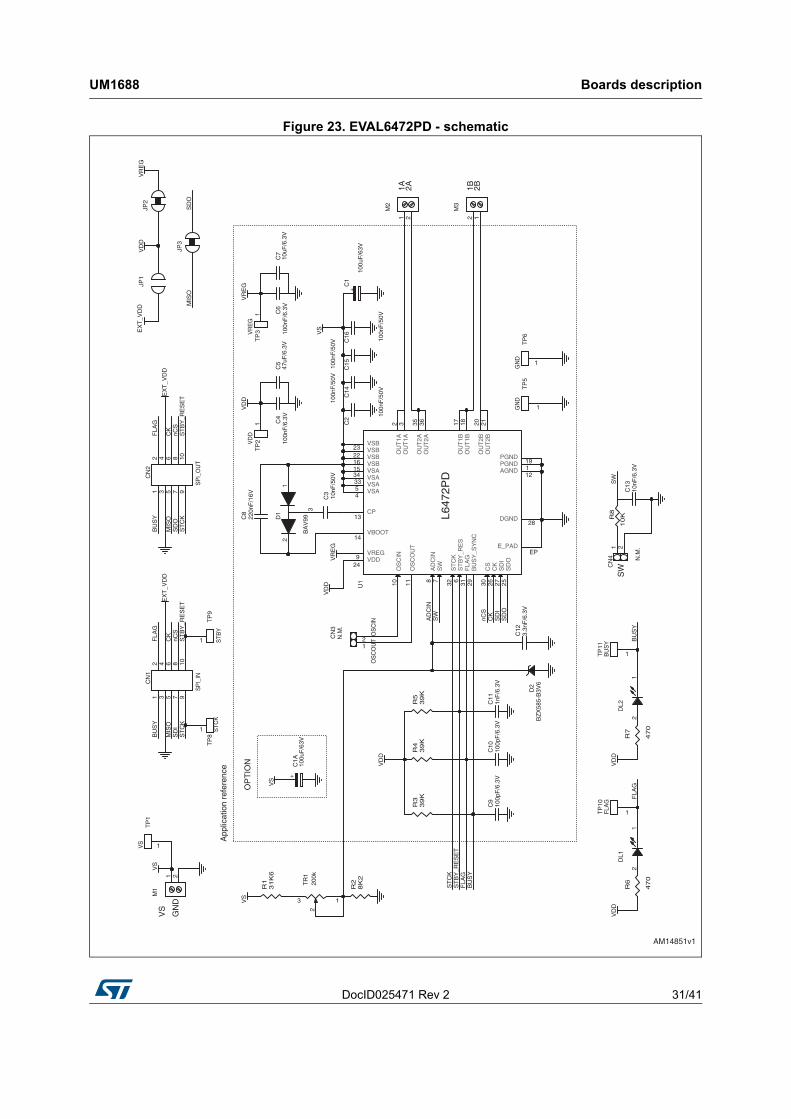
Figure 23. EVAL6472PD - schematic
1A 2A
SW
1B 2B
OS
CIN
OS
CO
UT
App
licat
ion
refe
renc
e
VS
GN
D
VD
DV
RE
G
SP
I_IN
SP
I_O
UT
FLA
GB
US
Y
OP
TIO
N
STC
KS
TBY
VS
GN
DG
ND
SW
MIS
OS
DI
CK
nCS
FLA
GB
US
Y
ST
CK
ST
BY
_RE
SE
T
MIS
OS
DO
CK
nCS
FLA
GB
US
Y
SD
OM
ISO
BU
SY
SD
IC
KnC
S
SW
ST
CK
AD
CIN
SD
O
FLA
GB
US
Y
FLA
GS
TB
Y_R
ES
ET
ST
CK
ST
BY
_RE
SE
T
VS
VS
EX
T_V
DD
EX
T_V
DD
EX
T_V
DD
VD
D
VR
EG
VR
EG
VD
D
VR
EG
VD
D
VD
D
VD
DV
DD
VS
VS
C5
47uF
/6.3
V
CN
21
23
45
67
89
10
TP
31
CN
4 N.M
.1 2R
8
10
K
C12
3.3n
F/6
.3V
R7
47
0
TP
9
1
C4
100n
F/6
.3V
R4
39
K
C2
100n
F/5
0V
C16 10
0nF
/50V
M2
1 2
C13
10nF
/6.3
V
TP
11
1
D1
BA
V99
12
3
TP
8
1
DL1
21
TP
10
1
JP2
TP
1
1
R3
39
K
D2
BZ
X58
5-B
3V6
TP
5
1
TR
120
0k
13
2
C1510
0nF
/50V
JP3
C7
10uF
/6.3
V+
C1A
100u
F/6
3V
C10
100p
F/6
.3V
M1
1 2
C14
100n
F/5
0V
DL2
21
R1
31
K6
R5
39
K
C3
10nF
/50V
U1
L6
47
2P
D
VDD24
VREG9
OS
CIN
10
OS
CO
UT
11
CP13
VBOOT14
AD
CIN
8
VSA4
VSA5
VSB15
VSB16 PGND
1
OU
T1A
2
OU
T2A
35
OU
T1B
17
OU
T2B
20AGND
12
SW
7
DGND28
BU
SY
_SY
NC
29F
LAG
31
SD
O25
SD
I27
CK
26C
S30
ST
BY
_RE
S6
ST
CK
32
OU
T1A
3
OU
T1B
18
OU
T2B
21
OU
T2A
36
VSB22
VSB23
VSA33
VSA34
PGND19
E_PADEP
C11
1nF
/6.3
V
JP1
CN
3N
.M.
12
CN
11
23
45
67
89
10
R6
47
0
M3
12
C6
100n
F/6
.3V
R2
8K
2
C9
100p
F/6
.3V
TP
21
TP
6
1
+C
1
100u
F/6
3V
C8
220n
F/1
6V
AM14851v1

Boards description UM1688
32/41 DocID025471 Rev 2
Table 20. EVAL6472PD - bill of material
Index Quantity Reference Value Package
1 1 CN1Pol. IDC male header vertical 10
poles (black)CON-FLAT-5X2-180M
2 1 CN2Pol. IDC male header vertical 10
poles (gray)CON-FLAT-5X2-180M
3 2 CN3, CN4 N.M STRIP254P-M-2
4 1 C1A 100 µF/63 V CAPE-R10HXX-P5
5 1 C1 100 µF/63 V CAPES-R10HXX
6 4 C2, C14, C15, C16 100 nF/50 V CAPC-0603
7 1 C3 10 nF/50 V CAPC-0603
8 2 C4, C6 100 nF/6.3 V CAPC-0603
9 1 C5 47 F/6.3 V CAPC-1206
10 1 C7 10 F/6.3 V CAPC-0805
11 1 C8 220 nF/16 V CAPC-0603
12 2 C9, C10 100 pF/6.3 V CAPC-0603
13 1 C11 1 nF/6.3 V CAPC-0603
14 1 C12 3.3 nF/6.3 V CAPC-0603
15 1 C13 10 nF/6.3 V CAPC-0603
16 1 JP1 LED red LEDC-0805
17 1 DL2 LED amber LEDC-0805
18 1 D1 BAV99 SOT23
19 1 D2 BZX585-B3V6 SOD523
20 1 JP1 Jumper OPEN JP2SO
21 2 JP2,JP3 Jumper CLOSED JP2SO
22 3 M1, M2, M3 Screw connector 2 poles MORSV-508-2P
23 1 R1 31.6 k RESC-0603
24 1 R2 8.2 k RESC-0603
25 3 R3, R4, R5 39 k RESC-0603
26 2 R6, R7 470 RESC-0603
27 1 R8 10 k RESC-0603
28 7TP1, TP2, TP3, TP8,
TP9, TP10, TP11TPTH-ring-1 mm (red) TH
29 2 TP5, TP6 TPTH-ring-1 mm (black) TH
30 1 TR1 200 k TRIMM-100x50x110-64W
31 1 U1 L6472 PowerSO36

DocID025471 Rev 2 33/41
UM1688 Boards description
41
Figure 24. EVAL6472PD - layout (inner layer2)
Figure 25. EVAL6472PD - layout (inner layer3)
AM14854v1
AM14855v1

Boards description UM1688
34/41 DocID025471 Rev 2
EVAL6472PD - thermal data
Figure 27. EVAL6472PD - thermal impedance graph
Figure 26. EVAL6472PD - layout (bottom layer3)
AM14856v1
0
2
4
6
8
10
1 10 100 1000 10000
12
AM14857v1
Time (seconds)
Zth
Zth
°C/W
DocID025471 Rev 2 35/41
UM1688 Evaluation environment setup
41
2 Evaluation environment setup
The evaluation environment is composed by:
One or more EVAL6470H\PD or EVAL6472H\PD.
One STEVAL-PCC009V2 demonstration board.
A USB cable.
A stepper motor with a small mechanical load (unloaded stepper motors suffer of strong resonance issues).
A power supply with an output voltage within the operative range of the evaluation board.
A Windows® 7 or Windows XP PC with a free USB port.
The SPINFamily evaluation tool (the last version can be downloaded from the STMicroelectronics® website).
In order to start using the evaluation environment the following steps are required:
1. Install the SPINFamily evaluation tool
2. Start the SPINFamily evaluation tool (by default it is in Start menu > All programs > STMicroelectronics > SPINFamily Evaluation Tool).
3. Select the proper device when requested by the application.
4. Plug the STEVAL-PCC009V2 demonstration board to a free USB port.
5. Wait a few seconds for board initialization.
6. Connect the SPI_IN connector (black) of the demonstration board to the 10-pin connector of the STEVAL-PCC009V2 board using the provided cable.For connecting more devices to the same board, please consult the daisy chain connection paragraph (Section 5: Daisy chaining on page 40).
7. Power-up the demonstration boards. The FLAG LED should turn on.
8. Click on the button with the USB symbol to connect the STEVAL-PCC009V2 board to the PC and initialize the evaluation environment.The application automatically identifies the number of demonstration boards connected.
9. The evaluation environment is ready.
Before start working with the demonstration board, the device must be configured according to the indications in Section 3: Device configuration.
Warning: Important - the device configuration is mandatory. The default configuration is not operative.

Device configuration UM1688
36/41 DocID025471 Rev 2
3 Device configuration
This section offers an overview of the basic configuration steps which are required for make the demonstration board operative.
Warning: Important - the device configuration is mandatory. The default configuration is not operative.
Important - before changing the device configuration verify that the device is in high impedance status (power stage is disabled).
3.1 Voltage mode driving (EVAL6470H/PD)
The configuration parameters of the voltage mode driving can be obtained through the BEMF compensation tool embedded into the SPINFamily software.
A wrong setup of these parameters could cause several issues, in particular:
The phase current decreases with the speed and the motor will stall.
The wrong voltage is applied to the motor and the system is very noisy.
The phase current reaches the overcurrent limit.
The BEMF compensation form uses the application parameters as inputs in order to evaluate the proper device setup.
The required inputs are:
Supply voltage.
Target phase current (r.m.s. value) at different motion conditions (acceleration, deceleration, constant speed and holding).
Target operating speed (maximum speed).
Motor characteristics.
The motor characteristics are: electrical constant (Ke), phase inductance and resistance. The inductance and the resistance of the phase are given in the motor datasheet. The Ke is rarely given in the specification and must be measured.
In the help section of the SPINFamily software a step by step procedure is explained. The same procedure can also be found in the application note “AN4144: Voltage mode control operation and parameter optimization” on www.st.com.
Click on the “evaluate” button to get the suggested setup for the voltage mode driving. Then click on “write” button to copy the data in the registers of the device.

DocID025471 Rev 2 37/41
UM1688 Device configuration
41
3.2 Advanced current control (EVAL6472H/PD)
The following configuration gives good results with most of motors:
Minimum ON time = 4 µs.
Minimum OFF time = 21 µs.
Max. fast decay = 10 µs.
Max. fast decay at step change = 16 µs.
Target switching time = 48 µs.
Predictive current control enabled.
The impact of the timing parameters are explained in the application note “AN4158: Peak current control with automatic decay adjustment and predictive current control: basics and setup”.
The target phase current is set through the TVAL registers. The TVAL determinates the current corresponding to the peak of the sine wave (microstepping operation).
3.3 Overcurrent and stall detection thresholds
The overcurrent protection and the stall detection (EVAL6470H\PD only) are implemented measuring the current flowing into each integrated MOSFET.
The overcurrent protection threshold should be set just above the current rating of the motor:
IOCDth > Imax,r.m.s. × √2
For example: if the maximum phase current of the motor is 2 Ar.m.s., the overcurrent protection should be set to about 3 A.
Warning: Important - it is strongly discouraged to disable the overcurrent shutdown. It may result in critical failures.
The stall detection threshold should be just above the operating peak current of the application. During the preliminary stages of evaluation, it can be set to the maximum value.
3.4 Speed profile
The max. speed parameter is the maximum speed the motor will run. By default, it is about 1000 step/s. That means, if you send a command to run at 2000 step/s, the motor speed is limited at 1000 step/s.
This is an important safety feature in the final application, but not necessarily useful to evaluate the device performances. Setting the parameter to high values (e.g. 6000 step/s) allows evaluating the maximum speed which can be achieved by the application under test through the speed tracking command (Run), but it probably limits the possibility to use positioning commands (Move, GoTo, etc.).

Device configuration UM1688
38/41 DocID025471 Rev 2
The Full-step speed parameter indicates the speed at which the system switches from microstepping to full step operation.
In voltage mode driving devices (EVAL6470H\PD), it is always recommended to operate in microstepping and not to switch to full step. Hence, this parameter should be greater than the maximum speed.

DocID025471 Rev 2 39/41
UM1688 How to change the supply configuration of the board
41
4 How to change the supply configuration of the board
The configuration of the supply voltages can be changed through the jumpers from J1 to J6 as listed in Table 21.
When VREG pin is supplied through an external voltage source, particular care must be taken in order to avoid that VS voltage falls below the VREG one (e.g. VS is floating and VREG is supplied). In this case the internal ESD diode is turned on and the device could be damaged.
Adding a low drop diode between VREG and VS protects the internal ESD diode from this event.
Table 21. Device supply configurations
Configuration JP1 JP2 Logic levels Notes
Logic supplied by the integrated voltage regulator and VDD shorted to VREG.
Open Closed3.3 V logic compliant.
Default.
Logic supplied by the integrated voltage regulator and VDD floating.
Open OpenAccording to VDD voltage.
The VDD must be supplied through the respective test point.
Logic supplied by the integrated voltage regulator and VDD supplied through the SPI connector.
Closed OpenAccording to VDD voltage.
The VDD must be supplied through the SPI connector.
Logic and VDD supplied through the SPI connector.
Closed Closed3.3 V logic compliant.
The supply voltage from the SPI connector must be 3.3 V.

Daisy chaining UM1688
40/41 DocID025471 Rev 2
5 Daisy chaining
More demonstration boards can be connected in daisy chain mode.
To drive two or more boards in daisy chain configuration:
1. Connect the STEVAL-PCC009V2 board 10-pin connector to the SPI_IN connector of the first demonstration board through the 10-pole flat cable.
2. Open the termination jumper (see Section 1.1: EVAL6470H on page 5, Section 1.2: EVAL6470PD on page 12, Section 1.3: EVAL6472H on page 21 and Section 1.4: EVAL6472PD on page 28).
3. Connect the SPI_OUT connector of the first demonstration board to the SPI_IN of the next one through the 10-pole flat cable.
4. Repeat point 2 and 3 for all the others board of the chain but the last one.
5. Check the termination jumpers of the demonstration boards: all the jumpers but the last one should be opened.
Note: Increasing the number of devices connected in chain could degrade SPI communication performances. If communication issues occur, try reducing the SPI clock speed.
6 Revision history
Table 22. Document revision history
Date Revision Changes
15-Nov-2013 1 Initial release.
16-Apr-2015 2
Updated Section : Introduction on page 1 (replaced “dSPINTM family devices” and “dSPINTM” by “L6470 and L6472 devices”).
Updated Section : Introduction on page 1 and Section 2: Evaluation environment setup on page 35 (replaced “SPIN family evaluation tool” by “SPINFamily evaluation tool”).
Removed Figure 3. EVAL6470H - layout (silk screen) from page 10, Figure 11. EVAL6470PD - layout (silk screen) from page 18, Figure 19. EVAL6472H - silkscreen from page 26, and Figure 27. EVAL6472PD - silkscreen from page 34.
Updated value in Table 5: EVAL6470H - bill of material on page 9, and packages in Table 10: EVAL6470PD - bill of material on page 17 and Table 20: EVAL6472PD - bill of material on page 32.
Minor modifications throughout document.

DocID025471 Rev 2 41/41
UM1688
41
IMPORTANT NOTICE – PLEASE READ CAREFULLY
STMicroelectronics NV and its subsidiaries (“ST”) reserve the right to make changes, corrections, enhancements, modifications, and improvements to ST products and/or to this document at any time without notice. Purchasers should obtain the latest relevant information on ST products before placing orders. ST products are sold pursuant to ST’s terms and conditions of sale in place at the time of order acknowledgement.
Purchasers are solely responsible for the choice, selection, and use of ST products and ST assumes no liability for application assistance or the design of Purchasers’ products.
No license, express or implied, to any intellectual property right is granted by ST herein.
Resale of ST products with provisions different from the information set forth herein shall void any warranty granted by ST for such product.
ST and the ST logo are trademarks of ST. All other product or service names are the property of their respective owners.
Information in this document supersedes and replaces information previously supplied in any prior versions of this document.
© 2015 STMicroelectronics – All rights reserved