etching of cubic gan by annealing in hydrogen ambient
TRANSCRIPT

Journal of Crystal Growth 189/190 (1998) 730—733
Etching of cubic GaN by annealing in hydrogen ambient
Hidenao Tanaka*, Atsushi NakadairaNTT Integrated Information and Energy Systems Laboratory, 3-9-11 Midori-cho, Musashino-shi, Tokyo 180, Japan
Abstract
Cubic GaN was annealed in different ambient gases at various temperatures from 800 to 950°C. It remained stable ininert gases, but it sublimated in hydrogen ambient. This sublimation was suppressed in H
2#NH
3and H
2#TEGa
mixtures. The sublimation rate in H2
can be controlled by changing the annealing temperature; the activation energy ofthe sublimation was estimated to be 37 kcal/mol. Observation of the anisotropic properties at the cross section of a stripeetched by this sublimation showed that (1 1 1)B surfaces were stabilized during the etching. To estimate the damageduring etching, we measured the photoluminescence from etched and rested surfaces. There was no difference in the shapeof the spectrum, and the decrease in intensity with etching was only 18% when the film thickness was reduced by15%. ( 1998 Elsevier Science B.V. All rights reserved.
PACS: 81.40.!z; 81.60.!j; 81.60.Cp; 82.65.Dp
Keywords: GaN; Cubic; Etching; Anisotropy; Sublimation; Thermal stability
1. Introduction
The wurtzite structure is a stable configurationfor group III nitrides. In addition, we can growmetastable cubic (zinc-blende structure) group IIInitrides on such substrates as GaAs, Si, 3C—SiC,and MgO, which have cubic symmetry. Cubic GaNis promising because its higher symmetry gives itseveral superior properties, such as easy cleavabil-ity for fabricating laser cavities. Although its crystal
*Corresponding author. Tel.: #81 422 59 3682; fax: #81422 59 2340; e-mail: [email protected].
quality has been improved to enable stimulatedemission by optical pumping [1], most of its phys-ical and chemical characteristics are still unclear.Determining its thermal stability is important foroptimizing its growth conditions and device pro-cesses. In this paper we report on the etching ofcubic GaN by sublimation in hydrogen ambient.
2. Experimental procedure
We grew cubic-GaN layers on (0 0 1) GaAs sub-strates by low-pressure metalorganic vapor-phaseepitaxy [2]. Triethylgallium (TEGa) and NH
3were
0022-0248/98/$19.00 ( 1998 Elsevier Science B.V. All rights reserved.PII S 0 0 2 2 - 0 2 4 8 ( 9 8 ) 0 0 2 7 4 - 7
used as source materials, and the substrate temper-ature was 950°C. The thickness of the GaN layerwas about 1.5 lm. After cleaving the cubic-GaNalong with the GaAs substrate to form a 5]5 mmsquare, we coated SiO
2all over the specimen by RF
sputtering. This SiO2
coating was important, be-cause it enabled us to reproduce the experiment.The SiO
2was patterned by photolithography, then
used as a pattern mask for thermal annealing. Tomeasure the sublimation rate, an SiO
2hole pattern
with a 1.5 mm diameter was used. To observe thecross-sectional etching pattern, a 3 lm wide linepattern was used. We annealed the specimens atvarious temperatures from 800 to 950°C using dif-ferent ambient gases: N
2, Ar, H
2, H
2#NH
3mix-
ture, and H2#TEGa mixture. The pressure in
a furnace was kept 76 Torr. In case of N2
and Ar,the gas flow rate was 4 lm. The total gas flow rate ofH
2mixture was 7 lm. After annealing, we removed
the SiO2
mask by HF solution. We then observedthe surface morphology and the cross section of thestripe pattern by scanning electron microscopy.The etching depth was measured at the edge of thepattern by a stylus instrument. We used photo-luminescence excited by a frequency-doubled Arion laser (257 nm) at room temperature to measurethe optical properties of the etched layers.
3. Results and discussion
The results of 15 min annealing at 950°C in sev-eral ambient gases are shown in Table 1. We foundno trace on the cubic GaN when annealed in inertgases, indicating that cubic GaN is stable at 950°Calthough it has a metastable configuration com-pared to hexagonal GaN. However, the cubic GaNdisappeared during annealing in H
2ambient. This
enhanced sublimation of cubic GaN by H2
is sim-ilar to that of hexagonal GaN reported by Mori-moto [3]. Apparently, the GaN#H
2changed into
Ga#NH3
and the Ga evaporated. This sublima-tion was suppressed in a mixture of gases contain-ing such reaction products as NH
3and Ga
precursor (TEGa) as shown in Table 1.The dependence of the sublimation rate on the
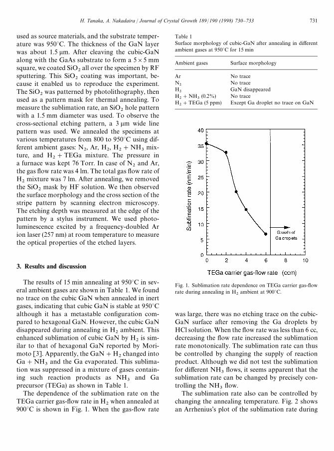
TEGa carrier gas-flow rate in H2
when annealed at900°C is shown in Fig. 1. When the gas-flow rate
Table 1Surface morphology of cubic-GaN after annealing in differentambient gases at 950°C for 15 min
Ambient gases Surface morphology
Ar No traceN
2No trace
H2
GaN disappearedH
2#NH
3(0.2%) No trace
H2#TEGa (5 ppm) Except Ga droplet no trace on GaN
Fig. 1. Sublimation rate dependence on TEGa carrier gas-flowrate during annealing in H
2ambient at 900°C.
was large, there was no etching trace on the cubic-GaN surface after removing the Ga droplets byHCl solution. When the flow rate was less than 6 cc,decreasing the flow rate increased the sublimationrate monotonically. The sublimation rate can thusbe controlled by changing the supply of reactionproduct. Although we did not test the sublimationfor different NH
3flows, it seems apparent that the
sublimation rate can be changed by precisely con-trolling the NH
3flow.
The sublimation rate also can be controlled bychanging the annealing temperature. Fig. 2 showsan Arrhenius’s plot of the sublimation rate during
H. Tanaka, A. Nakadaira / Journal of Crystal Growth 189/190 (1998) 730–733 731

Fig. 2. Sublimation rate versus reciprocal of temperature dur-ing annealing in H
2ambient.
annealing in H2
ambient. The activation energywas estimated to be 37 kcal/mol from the slope. Incomparison with hexagonal GaN, this activationenergy is similar to that of sublimation in H
2ambi-
ent (34 kcal/mol) [4] and smaller than that in a vac-uum (75 kcal/mol) [5]. The similar activationenergy indicates that the enhanced sublimation byH
2depends on the chemical reaction between the
Ga—N bond and H2.
In our experiments, although we used differentepitaxial films, the sublimation rate did not dependon the epitaxial lot number. But when we did notcoat the GaAs substrate with SiO
2, the rate was
often smaller, apparently because the Ga evapor-ated from the GaAs substrate. Therefore, the SiO
2coating is very important for reproducing the subli-mation.
Anisotropic properties are usually observedwhen the chemical reaction is the limiting factor inthe etching. Cross-sectional scanning electronmicrographs of a cubic-GaN stripe etched by subli-mation in H
2ambient are shown in Fig. 3. A mesa
shape was observed in the [1 1 0] direction, and an
Fig. 3. Cross-sectional scanning electron micrographs of cubic-GaN stripe in different directions.
inverse-mesa shape was observed in the [1 11 0]direction. These results show that the (1 1 1)B sur-face was stabilized during annealing in H
2. In the
anisotropic etching of III—V materials using chem-ical solutions, generally the (1 1 1)A surface is sta-bilized because the etching is limited by thereaction of the group-III materials. In contrast,group-V materials limit the reaction in sublimationetching in H
2. In other words, N disconnection
limits sublimation etching.To use this etching for device fabrication, dam-
age to the crystal during etching must be mini-mized. We measured the photoluminescence fromthe crystal to estimate the damage caused by subli-mation etching. As shown in Fig. 4, there was nodifference in shape in the spectra of photolumines-cence from etched and remained surfaces. There-fore, the radiative defects were very small. Thedecrease in intensity with etching was only 18%,and the film thickness was reduced by 15% byetching. The film thickness was relatively thin com-pared to the carrier diffusion length, therefore, theintensity decrease is mainly due to the difference in
732 H. Tanaka, A. Nakadaira / Journal of Crystal Growth 189/190 (1998) 730–733
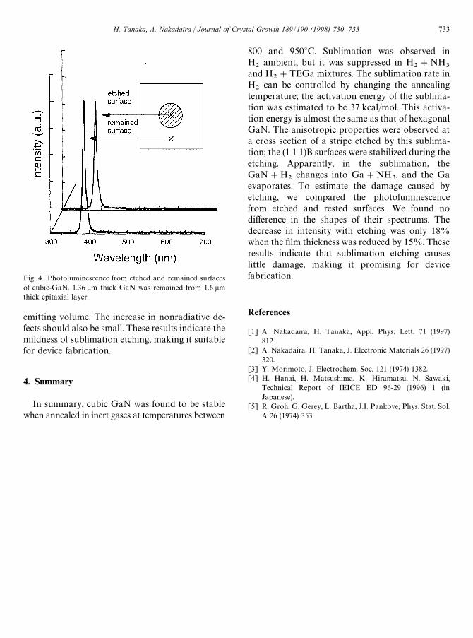
Fig. 4. Photoluminescence from etched and remained surfacesof cubic-GaN. 1.36 lm thick GaN was remained from 1.6 lmthick epitaxial layer.
emitting volume. The increase in nonradiative de-fects should also be small. These results indicate themildness of sublimation etching, making it suitablefor device fabrication.
4. Summary
In summary, cubic GaN was found to be stablewhen annealed in inert gases at temperatures between
800 and 950°C. Sublimation was observed inH
2ambient, but it was suppressed in H
2#NH
3and H
2#TEGa mixtures. The sublimation rate in
H2
can be controlled by changing the annealingtemperature; the activation energy of the sublima-tion was estimated to be 37 kcal/mol. This activa-tion energy is almost the same as that of hexagonalGaN. The anisotropic properties were observed ata cross section of a stripe etched by this sublima-tion; the (1 1 1)B surfaces were stabilized during theetching. Apparently, in the sublimation, theGaN#H
2changes into Ga#NH
3, and the Ga
evaporates. To estimate the damage caused byetching, we compared the photoluminescencefrom etched and rested surfaces. We found nodifference in the shapes of their spectrums. Thedecrease in intensity with etching was only 18%when the film thickness was reduced by 15%. Theseresults indicate that sublimation etching causeslittle damage, making it promising for devicefabrication.
References
[1] A. Nakadaira, H. Tanaka, Appl. Phys. Lett. 71 (1997)812.
[2] A. Nakadaira, H. Tanaka, J. Electronic Materials 26 (1997)320.
[3] Y. Morimoto, J. Electrochem. Soc. 121 (1974) 1382.[4] H. Hanai, H. Matsushima, K. Hiramatsu, N. Sawaki,
Technical Report of IEICE ED 96-29 (1996) 1 (inJapanese).
[5] R. Groh, G. Gerey, L. Bartha, J.I. Pankove, Phys. Stat. Sol.A 26 (1974) 353.
H. Tanaka, A. Nakadaira / Journal of Crystal Growth 189/190 (1998) 730–733 733