esd simulation with wunsch-bell based behavior modeling ... · pdf fileesd simulation with...
TRANSCRIPT
ESD Simulation with Wunsch-Bell based BehaviorModeling Methodology
Yiqun Cao (1, 2), Ulrich Glaser (1), Joost Willemen (1), Filippo Magrini (1),
Michael Mayerhofer (1), Stephan Frei (2), Matthias Stecher (1)(1) Infineon Technologies, Am Campeon1-12, D-85579, Neubiberg, Germany
tel.: +49 89 234 63936, E-mail: [email protected]
(2) Technische Universität Dortmund, Campus Nord, ET-Geb., Friedrich-Wöhler-Weg 4, D-44227, Dortmund, Germany
Abstract – Conventional modeling methods for ESD protection can be specific to device types or cannotreproduce the self-heating effect. This work proposes a straightforward modeling methodology based on theWunsch-Bell characterization method using TLP. It allows precise ESD simulation verified by measurements.
I. IntroductionTraditional simplified models of on-chip ESD devicesand structures reproduce their quasi-static I/Vcharacteristics without concerning self-heating duringESD [1, 2]. In fact, as given by the Wunsch-Belltheory, the failure levels (failure power and failureenergy) of semiconductor structures due to thermalrun-away strongly depend on the pulse width (tw) [3].The power to failure as function of pulse width hasdifferent slopes between adiabatic region andWunsch-Bell region according to the Dwyer’s work[4]. In the ESD concepts, the ESD protection elementsare designed to be firstly damaged above the ESDtarget level, and the modeling of ESD protectionelements up to the high-current density regime or upto the failure level is of prime importance. Besides thefailure levels, also the on-resistance (Ron) whichdirectly affects the transient response of the ESDprotections differs significantly because of self-heating when the ESD elements are carrying differentpulse energies with different pulse durations. In fact,the ESD requirements of the semiconductor productshave become very manifold nowadays. Due todifferent ESD standards from CDM, HBM to system-level ESD with various pulse forms one has to expectdifferent behavior of the ESD structures with respectto self-heating. Further, the robustness of ESDelements stressed by pulses which are even beyondESD range such as EOS pulses has also gainedincreasing interest [5, 6]. Hence the thermal effectsand the modification of Ron in terms of stress durationneed to be taken into account for the modeling issues.
Apart from many compact physical models which areavailable for SPICE simulation [7-11], this workintroduces a novel Wunsch-Bell based behaviormodeling methodology which basically considers theESD structure or protected I/O pin as a black-box. Asthe electro-thermal simulation or thermal equivalentcircuits often required for physics-based models arenot necessary any more in the proposed behaviormodeling method, technology parameters and devicegeometries are out of concern simplifying themodeling significantly. I/V properties as well as thefailure levels of the device of interest can be simplycharacterized with TLP in a wide pulse range. Thebehavior modeling itself is language-independent.VHDL-AMS is chosen in this work for modeling. Inprior publications, the behavior modelingmethodologies using ETABLE operator [12] or
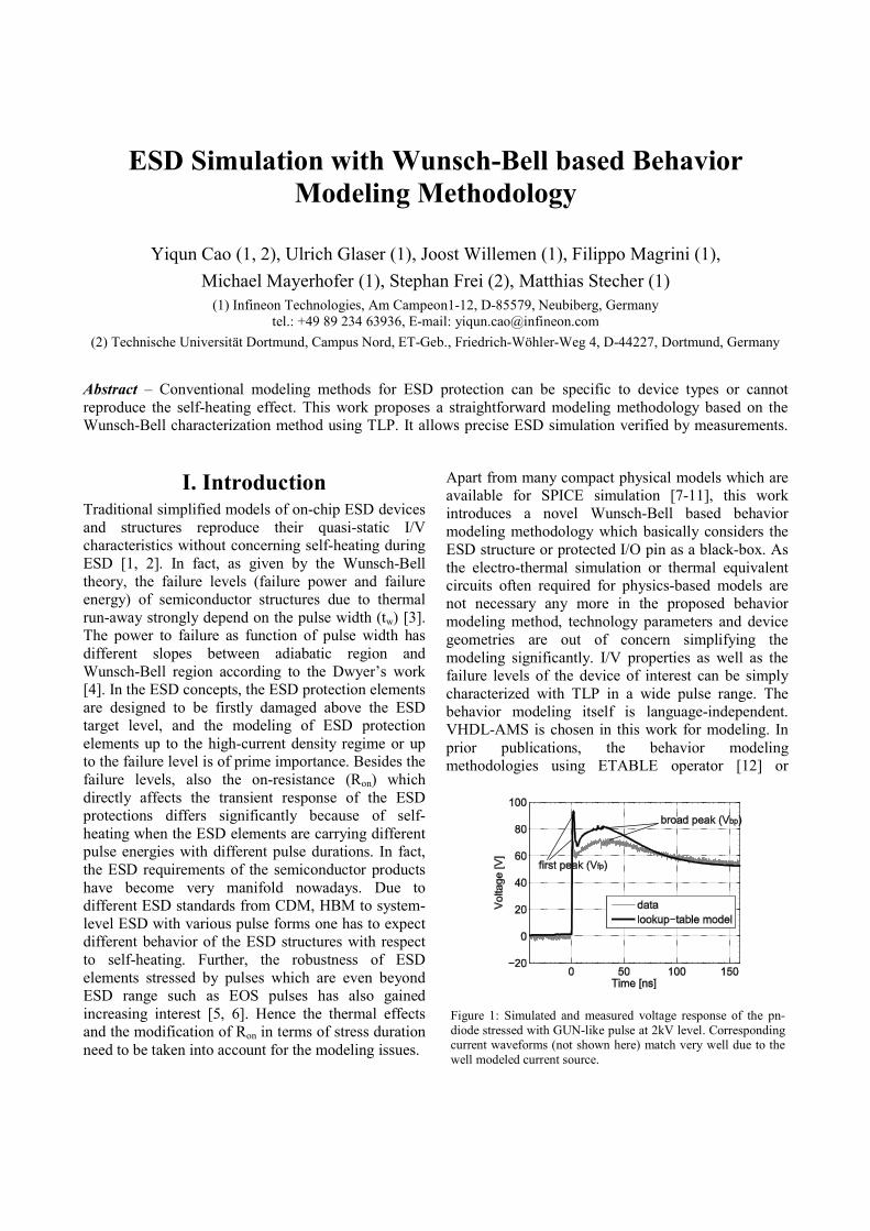
Figure 1: Simulated and measured voltage response of the pn-diode stressed with GUN-like pulse at 2kV level. Correspondingcurrent waveforms (not shown here) match very well due to thewell modeled current source.

lookup-table [13] focus mainly on the devicecharacterizations with 100ns TLP. They can have verygood usage for ESD simulation if self-heating in theprotection elements is negligible. It is however shownin [14] with 100ns TLP characteristic only, that themodel quality is not satisfying if an IEC 61000-4-2[15] system-level ESD pulse (hereafter called GUNpulse) is applied to the modeled pn-diode (Fig. 1). Forthe stress-level higher than 2kV, the deviation ofmeasurement data and model becomes even larger.
The modeling method in this work focuses on the onehand on the self-heating behavior and enables on theother hand the prediction of the robustness of theprotection structures under various ESD stresses. Thedetailed modeling methodology is described in sectionII. Since the individual physical details are notrequired, the proposed methodology can be generallyapplied to model different types of ESD devices orprotection networks. Three modeling examples forvarious types of ESD protections are introduced insection III. In addition, ESD simulation is performedin the co-design of on- and off-chip ESD protectionsto estimate their robustness in section IV. System-level ESD tests confirm the simulation results.
II. Modeling MethodologyAiming at successful ESD simulations, the model hasto reproduce the transient responses of the ESDelements at first. Based on that, the power and energydissipated in the modeled devices can be accuratelycalculated from correctly simulated voltage andcurrent waveforms. The failure or the robustness of
the ESD structure is then well predictable.
In this work, the ESD devices are characterized usingInfineon TLP equipment with tw from 5ns to 1.5μs. It aims to cover a wide pulse range from component- tosystem-level ESD requirements. Fig.2 illustratesschematically the TLP characterization for abreakdown device using different pulse widths. Thecharacterization method as well as the measurementsetup is similar as described in [10]. In Fig. 2, themodeling principle is qualitatively shown based on abreakdown ESD device with two linear on-resistancesRon, 1 and Ron, 2. In practical cases, more than two Ron
can be defined depending on the complexity of thedevice behavior and the target model accuracy. I/Vcurves derived from the different average windowscorrespond to different pulse durations tw1, tw2 and tw3.The calculated I/V point from the current and voltagetransients in Fig. 2 (a) is marked in Fig. 2 (b) for eachtw. Note that with self-heating, the voltage across thedevice increases with increasing pulse width while thecurrent decreases. Self-heating takes noticeable effectshowing tw-dependent Ron. The device modelingreflects this device behavior by using a fittingfunction Ron=f(tw) within a linear segment of the I/Vcurves. In this example, two Ron (Ron, 1 and Ron, 2) asfunctions of tw are modeled. The quality of the Ron
fitting functions relies on the numbers of tw used inthe TLP characterization.
During the simulation, Ron is modified for every timestep taking the effective pulse width into account:
ǡ௧భ ൌ ሺݐ௪ ൌ ଵݐ െ (ݐ
where t1 is the present time instant and t0 is the ESDdevice turn-on time which is detected by the model. Atime instant is considered as t0 when the currentthrough the modeled ESD element exceeds a pre-defined limit or the voltage across the modeled ESDelement reaches the trigger voltage (Vtr). Hence t0 isin general not equal to the start time of the pulsegeneration. The present voltage and current valuesV(t1) and I(t1) are self-consistently calculated by thesimulator with the appropriate Ron,t1.
Fig. 3 illustrates the principle of building thethresholds of power to failure (Pf) or energy to failure(Ef) into the model with the fitting functions Pf=f(tw)or Ef=f(tw). A power law is adequate for devices suchas pn-diodes within the Wunsch-Bell region [16]. Inthe simulation, the failure level limit at t1, Ef, t1, isgiven by the energy Ef(tw=t1-t0). The energy dissipatedin the device is calculated as
௧భܧ ൌ න (ݐ)ܫ ή(ݐ)ݐ௧ୀ௧భ
௧ୀ௧బ
Figure 2: Based on (a) TLP characterization using the averagewindows of tw1, tw2 and tw3, (b) Ron, 1 and Ron, 2 are derived fromaveraged voltage and current transients as functions of tw.
Figure 3: Ef as function of tw (b) derived from failure current andvoltage in TLP characteristics (a).
The modeled device is considered as thermallydamaged if the condition Et1<Ef(tw) is violated at time.Fig. 4 gives the simplified modeling flow where allthe fitting functions are defined by the Wunsch-Bellcharacterization. Note that by means of Wunsch-Bellcharacterization, the choice of the pulse duration isnot only limited to the Wunsch-Bell region. Thefitting function of failure power does not have tofollow the power law. In addition, for ESD structureseventually having electrical limits such as activeclamps [16], maximal allowed power (Pmax) is used asthe additional failure criterion.
III. Models of ESD Structures
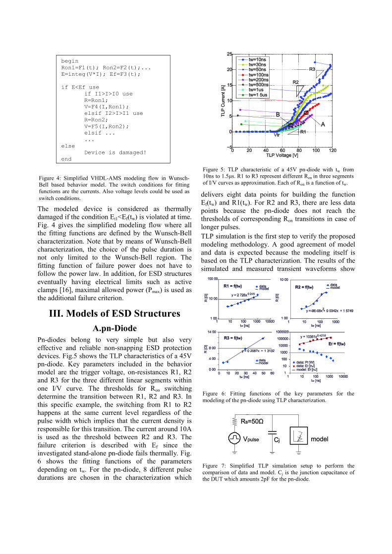
A.pn-DiodePn-diodes belong to very simple but also veryeffective and reliable non-snapping ESD protectiondevices. Fig.5 shows the TLP characteristics of a 45Vpn-diode. Key parameters included in the behaviormodel are the trigger voltage, on-resistances R1, R2and R3 for the three different linear segments withinone I/V curve. The thresholds for Ron switchingdetermine the transition between R1, R2 and R3. Inthis specific example, the switching from R1 to R2happens at the same current level regardless of thepulse width which implies that the current density isresponsible for this transition. The current around 10Ais used as the threshold between R2 and R3. Thefailure criterion is described with Ef since theinvestigated stand-alone pn-diode fails thermally. Fig.6 shows the fitting functions of the parametersdepending on tw. For the pn-diode, 8 different pulsedurations are chosen in the characterization which
delivers eight data points for building the functionEf(tw) and R1(tw). For R2 and R3, there are less datapoints because the pn-diode does not reach thethresholds of corresponding Ron transitions in case oflonger pulses.
TLP simulation is the first step to verify the proposedmodeling methodology. A good agreement of modeland data is expected because the modeling itself isbased on the TLP characterization. The results of thesimulated and measured transient waveforms show
Figure 5: TLP characteristic of a 45V pn-diode with tw from10ns to 1.5μs. R1 to R3 represent different Ron in three segmentsof I/V curves as approximation. Each of Ron is a function of tw.
Figure 6: Fitting functions of the key parameters for themodeling of the pn-diode using TLP characterization.
Figure 7: Simplified TLP simulation setup to perform thecomparison of data and model. Cj is the junction capacitance ofthe DUT which amounts 2pF for the pn-diode.
Figure 4: Simplified VHDL-AMS modeling flow in Wunsch-Bell based behavior model. The switch conditions for fittingfunctions are the currents. Also voltage levels could be used asswitch conditions.
beginRon1=F1(t); Ron2=F2(t);...E=integ(V*I); Ef=F3(t);
if E<Ef useif I1>I>I0 useR=Ron1;V=F4(I,Ron1);elsif I2>I>I1 useR=Ron2;V=F5(I,Ron2);elsif ......
elseDevice is damaged!
end

excellent agreement with a wide range of pulsedurations. Fig. 7 depicts the schematic of a verysimplified TLP setup in the simulation. Fig.8 showsexemplary the simulated transients overlapped by theexperimental results for 100ns TLP. Thecorresponding I/V pairs (“A” and “B”) are marked inFig. 5. Note the different levels of self-heating in thepn-diode in low and high current density regions. Inaddition to the waveform comparison, Fig. 9 showsthat the behavior model reproduces also the failurelevels. A 1µs TLP pulse is taken as an example. Thewaveforms of the last stress before failure and thefailing stress clearly show the correct estimation ofthe simulated failure levels. As soon as the device isconsidered as damaged, the model will switch theESD device to low impedance (e.g. 1Ω) to represent nearly a short after device failure. As a result, the
current and voltage transients will change abruptly inthe simulation and the device failure can be easilydistinguished in the simulated waveforms. Error orwarning message is certainly delivered as well.
In addition to the TLP simulation, ESD-like pulseswith non-square waveform are more practical andconvincing for the validation of the modeling method.Fig. 10 compares the failure levels of the pn-diodestressed by GUN-like pulses applying wafer-leveltests [17]. The same failure current is found insimulation and measurement. Moreover, the voltagetransients clearly show the improved reproductioncapability of the proposed modeling methodologyincluding self-heating compared to the 100ns TLPbased method in Fig. 1.
B. Active ClampStandard active clamps as a type of non-snappinghigh-voltage ESD protection circuits have gainedincreasing attention recently [16, 18]. As discussed,the Wunsch-Bell based methodology can easily beadapted to various types of protection elementswithout the deep knowledge of physical details.Nevertheless, the understanding of the devicebehavior is also essential. The main difference of theZener-triggered active clamps compared to the pn-diodes from a modeling aspect is the transient turn-onbehavior with respect to the capacitive gate coupling.The Zener-trigger defines the static trigger voltage ofthe active clamp. The DMOS transistor is designed toturn on and conduct ESD current for VDS>Vtr. The
Figure 10: Simulated and measured waveforms for the pn-diodestressed by GUN-like pulses at 6kV stress level (stress tofailure). Thermal destruction is observed both in simulation andmeasurement.
Figure 9: Comparison of Wunsch-Bell based model and TLPdata for1µs TLP regarding the failure levels of the pn-diode.
Figure 8: Comparison of Wunsch-Bell based model and TLP datawith respect to transient responses of the pn-diode for tw=100ns.“A” and “B” denote the corresponded I/V waveforms.

transistor is supposed to be off if VDS does not exceedVtr. However for VDS<Vtr the capacitive coupled gate-source voltage can still turn on the transistortransiently. After the RGSCGS discharging, thetransistor is turned off when VGS goes below thethreshold voltage of the DMOS. Fig. 11 shows theschematic of the active clamp circuitry as well as thetransient turn-on behavior illustrated with the TLPwaveforms for VDS<Vtr.
Spectre modeling approach [16] could be involved toaccurately model the parasitic capacitances and theDMOS transistor. The consideration of self-heatingunder ESD conditions would be very complicated thisway. In the contrary, the proposed behavior modelingin this work assumes that the active clamp exhibits afinite on-resistance for V<Vtr under short pulses. Thiseffectively translates the transient turn-on of the activeclamps into a tw dependent Ron. Fig. 12 shows the TLPcharacteristics of a 25V active clamp: here R1 is
defined for the segment between 0V and Vtr. Fig. 13shows the agreement of data and model for 100nsTLP with different voltage and current pairs indicatedin Fig. 12.
For the failure estimation of the active clamps, Pmax isbuilt in the model as electrical limit in addition to Ef.Simulation and measurement with GUN-like pulsesconfirms the prediction of the electrically induced
Figure 12: TLP characteristic of a 25V active clamp with tw from5ns to 1.5μs. R1 represents the transient turn-on behavior ofactive clamp where R2 and R3 represent different Ron after Vtr isreached.
Figure 13: Comparison of Wunsch-Bell based model and TLPdata with respect to transient responses of the active clamp. “A”,“B” and “C” denote the corresponded I/V waveforms.
Figure 14: Simulated and measured waveforms for the activeclamp stressed by GUN-like pulses at 3kV GUN level (stress tofailure). Electrical failure is observed both in simulation andmeasurement.
Figure 11: (a) The schematic of a Zener-triggered active clampwith gate discharge resistor RGS and gate protection ZD,GS. (b)The transient turn-on of the DMOS due to gate coupling showingtypical I/V waveforms when the stress voltage is below thedesigned Vtr.

failure and the failure level as shown in Fig. 14. Notethat the transient voltage after the device damage isnot meant to be correctly modeled. The siliconmelting in the device after damage exhibits a timedependent degradation leading to leakage increase. Inthe simulation however, the device model is simplyswitched to a 1Ω resistance to identify the failure.
C. npn-BJTModeling of snapping ESD structures oftenencounters convergence problems in simulations.However, the behavior modeling methodology can beapplied to snapping ESD elements without sufferingfrom convergence issues. An npn-BJT implemented ina power technology is used as the third modelingexample exhibiting a snapback characteristic. TheTLP characteristics with diverse pulse durations areshown in Fig. 15. Note that for tw=5ns, the holdingvoltage Vh seems to be larger than for larger tw. Thisis caused by the snapback process of the bipolartransistor which takes several nanoseconds. Thetransient snapback from the trigger voltage to theholding voltage can last longer than 5ns. The averagedvoltage is thus larger than the real Vh in the steadyclamping state. Similar to the modeling of thetransient turn-on behavior of active clamps, the virtualtw-dependence of Vh can be utilized in the modeling toreproduce the snapback process of the device. Withthis consideration, one can use the proposedmethodology to implement behavior models forsnapping ESD devices with complex turn-on and self-heating effects. Fig. 16 confirms the agreementbetween model and measurement data with respect totransient waveforms in 100ns TLP. “A” to “C”indicate again the voltage and current waveformscorresponding to the I/V points in the TLP
characteristics (Fig. 15).
For the validation of the device model in reproducingthe failure level, the same GUN-like pulse generatoras in the study of non-snapping ESD protectionelements is applied to the npn-BJT. The device failsthermally at 2.5kV according to both, simulation andmeasurement (Fig. 17).
As a conclusion for the modeling examplesdemonstrated in this section, the Wunsch-Bell based
Figure 15: TLP characteristics of the npn-BJT with tw from 5nsto 0.5μs. R1, R2 represent different Ron before and after thetriggering of the snapback. Each of Ron is a function of tw.
Figure 16: Comparison of Wunsch-Bell based model and TLPdata regarding transient responses of the npn-BJT. “A”, “B” and“C” denote the corresponding I/V waveforms.
Figure 17: Simulated and measured waveforms for the npn-BJTstressed by GUN-like pulses at 2.5kV GUN level (stress tofailure). Thermal failure is observed both in simulation and test.

behavior modeling is widely applicable for differenttypes of ESD devices and circuits. The investigatedstand-alone structures are modeled to reproduce self-heating and failure levels which are validated withexperimental data.
IV. Application
A. ESD Co-Design on PCBAs the on-chip ESD protection elements arecharacterized and described in VHDL-AMS, one ofthe most interesting applications of the models is theprediction of system-level ESD robustness. Toachieve the ESD target level of the circuit on board,the co-design of on- and off-chip protection elementsis often necessary. Capacitor, varistor, TVS-diode etcetera are commonly employed as off-chip ESDprotection elements. Accurate ESD simulationssubstantially help to select the proper off-chip devicesin the system (PCB) design in an early stage of theproject.
Combinations of diverse on-chip protection elementswith off-chip devices are simulated and measuredshowing the straightforward application of theproposed modeling methodology. In the simulationsetups, a discharge lumped element network includingparasitic RLC is used as a common ESD generator(GUN) model.
For the verification by measurements, the on-chipESD devices introduced earlier are assembled in theplastic package LQFP-64 and placed in a test socketon PCB. The ESD generator TESEQ NSG438(150pF/330Ω) is used to perform the system-level ESD tests. Fig. 18 shows a fraction of the test boardwith external devices and the IC socket. Curve traceafter each stress is used for monitoring the leakagecurrent as well as for detecting the failure level in theGUN tests.
The stand-alone active clamp fails electrically at 3kVstress level of GUN-like pulses as discussed in sectionIII. The same failure level is confirmed by real GUNtests using the ESD generator. The simulation predictsan improved total ESD robustness of about 6.5kV inconnection with a parallel 6.8nF ceramic capacitor.The on-chip active clamp will fail thermally ratherthan electrically according to the simulatedwaveforms (Fig. 19). This result is validated byapplying GUN tests where the failure occurs at 6.5kVto 7kV stress levels.
Another example of ESD co-design is implementedby using the 45V pn-diode as on-chip protection. Avaristor with typical turn-on voltage of 60V is used asthe off-chip ESD device (Fig. 20). The turn-onvoltage is a little larger than Vtr of the on-chip diode(Fig. 5). Note that the model of the varistor is simply
Figure 18: Photograph of the test PCB. Board traces, packageand socket parasitics have negligible impact on the system-levelESD robustness in this design.
Figure 19: Simulated waveforms of a 6.8nF ceramic capacitor inparallel to an on-chip 25V active clamp under GUN stress. Thecurrent distribution is shown at 6.5kV. The failing stress causedby thermal breakdown of the active clamp occurs at 7kV.
Figure 20: 100ns TLP characteristic of the varistor. The model isgenerated merely using 100ns TLP without self-heating effect.
generated using 100ns TLP curves since the self-heating of off-chip devices is usually not as importantas for the on-chip devices due to their very highenergy dissipation capability. The stand-alone diodefails at approximately 6kV GUN stress. According tothe simulation the failure level of the combined ESDprotection will increase significantly to 19kV due tothe contribution of the varistor. This is againconfirmed by test results.
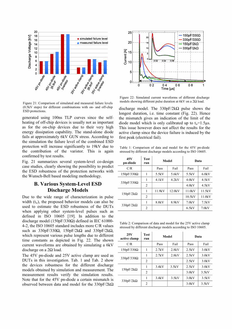
Fig. 21 summarizes several system-level co-designcase studies, clearly showing the possibility to predictthe ESD robustness of the protection networks withthe Wunsch-Bell based modeling methodology.
B. Various System-Level ESDDischarge Models
Due to the wide range of characterization in pulsewidth (tw), the proposed behavior models can also beused to estimate the ESD robustness of the DUTswhen applying other system-level pulses such asdefined in ISO 10605 [19]. In addition to thedischarge model (150pF/330Ω) defined in IEC 61000-4-2, the ISO 10605 standard includes more C/R valuessuch as 330pF/330Ω, 150pF/2kΩ and 330pF/2kΩ, which represent various pulse lengths due to differenttime constants as depicted in Fig. 22. The showncurrent waveforms are obtained by simulating a 6kVdischarge on a 2Ω load.
The 45V pn-diode and 25V active clamp are used asDUTs in this investigation. Tab. 1 and Tab. 2 showthe devices robustness for the different dischargemodels obtained by simulation and measurement. Themeasurement results verify the simulation results.Note that for the 45V pn-diode a certain mismatch isobserved between data and model for the 330pF/2kΩ
discharge model. The 330pF/2kΩ pulse shows the longest duration, i.e. time constant (Fig. 22). Hencethe mismatch gives an indication of the limit of thediode model which is only calibrated up to tw=1.5µs.This issue however does not affect the results for theactive clamp since the device failure is induced by thefirst peak (electrical fail).
Table 1: Comparison of data and model for the 45V pn-diodestressed by different discharge models according to ISO 10605.
45Vpn-diode
Testrun
Model Data
C/R Pass Fail Pass Fail
150pF/330Ω 1 5.5kV 5.6kV 5.5kV 6.0kV
330pF/330Ω 1 4.1kV 4.2kV 4.0kV 4.5kV
2 4.0kV 4.5kV
150pF/2kΩ 1 11.9kV 12.0kV 11.0kV 11.5kV
2 10.5kV 11.0kV
330pF/2kΩ 1 8.8kV 8.9kV 7.0kV 7.5kV
2 6.5kV 7.0kV
Figure 22: Simulated current waveforms of different dischargemodels showing different pulse duration at 6kV on a 2Ω load.
Table 2: Comparison of data and model for the 25V active clampstressed by different discharge models according to ISO 10605.
25Vactive clamp
Testrun
Model Data
C/R Pass Fail Pass Fail
150pF/330Ω 1 2.7kV 2.8kV 2.5kV 3.0kV
330pF/330Ω 1 2.7kV 2.8kV 2.5kV 3.0kV
2 2.5kV 3.0kV
150pF/2kΩ 1 3.4kV 3.5kV 2.5kV 3.0kV
2 3.0kV 3.5kV
330pF/2kΩ 1 3.4kV 3.5kV 3.0kV 3.5kV
2 3.0kV 3.5kV
Figure 21: Comparison of simulated and measured failure levels(0.5kV steps) for different combinations with on- and off-chipESD protections.

V. Conclusions
The presented behavior modeling method is portableand easy-to-implement. Good correlations betweensilicon measurements and simulations have beenachieved validating the methodology and the models.Details of the application examples including system-level ESD co-design and impact of different pulses onthe robustness of the ESD devices are given. Duringthe Wunsch-Bell characterization a wafer-level TLPsetup is used which minimizes parasitic effects. In thesystem-level tests, the parasitic of the used test PCB,package and socket has no significant impact on therobustness of the devices since the models are in mostcases valid according to the simulation results. Themain advantage of the proposed modelingmethodology is the behavior description based on theprofound TLP measurements. It avoids the emulationof physical parameters or circuit details which can bearbitrary complicated. The presented methodologyeasily allows generalizing the modeling method todifferent types of ESD protection elements. On theother hand, the main drawback of the proposedbehavior model is also due to the lack of the physicalbasis. The self-heating effect is obtained with thefitting function Ron=f(tw) which is derived from theTLP tests. In the reality the pulse waveforms differusually a lot from the rectangular TLP pulses.Fortunately, most of the real pulses exhibitexponential decay, where at the tale of the pulse thecurrent level is low enough so that the self-heating isnot significant anymore. The inaccuracy of the Ron
estimation in this pulse part is therefore ignorable.
Furthermore, the range of application of the behaviormodeling can be extended. In this study, the model isvalid up to 1.5µs. An extended characterization up tothe milliseconds range enables the simulation of therobustness of protected devices stressed by EOSdisturbances such as defined in ISO 7637 [20-22].Moreover, for on-chip ESD design, with the ESDwindow given by the circuits being protected,different types of protection schemes can be simulatedusing the introduced modeling method to achieve theoptimal design considering the area consumption andtarget robustness. The underestimation of the ESDdevice capability due to models without self-heating(Fig. 1) can lead to ESD overdesign and must beavoided in a cost efficient design.
AcknowledgementsThe authors gratefully thank Professor Dr. DionyzPogany for the review and excellent mentoring work.
This work was supported by the MEDEA+ project2T205 SPOT-2.
References[1] W. Li et al., “A Scalable Verilog-A ModelingMethod for ESD Protection Devices,” in Proc.EOS/ESD, 2010, pp. 1A. 1-10.
[2] M. Mayerhofer et al., “ESD Review Methodologyusing Transient Simulations on Circuit Level and itsApplication for JEDEC/ESDA HBM and IEC 61000-4-2 Pulses in Automotive Circuits,” in Proc. ESDForum e.V., 2009, pp. 129-139.
[3] D.C. Wunsch and R.R. Bell, “Determination ofThreshold Failure Levels of Semiconductor Diodesand Transistors due to Pulse Voltages,” IEEE Trans.Nuc. Sci., NS-15, pp. 244-259, 1968.
[4] V.M. Dwyer, A.J. Franklin and D.S. Campbell,“Thermal Failure in Semiconductor Devices,” Solid-State Electronics, Vol. 33, No. 5, pp. 553-560, 1990.
[5] B. Deutschmann, et al., “Robustness of ESDProtection Structures against Automotive TransientDisturbances,” in Proc. APEMC, 2010.
[6] F. Magrini et al., “Correlation between SystemLevel Robustness and TLP Results of ESD Devices,”in IEW, 2011.
[7] H. Wolf et al., “Pulsed Characterization of areverse biased pn-Junction for ESD HBMSimulation.” Microelectronics and Reliability, Vol.36, Issues 11-12, pp. 1711-1714, 1996.
[8] C. Torres et al., “Modular, Portable, and EasilySimulated ESD Protection Networks for AdvancedCMOS Technologies,” in Proc. EOS/ESD, 2001.
[9] M. Khazhinsky et al., “ESD Protection forAdvanced CMOS SOI Technologies,” in Proc.EOS/ESD, 2005.
[10] M. Stockinger et al., “Characterization andModeling of Three CMOS Diode Structures in theCDM to HBM Timeframe,” in Proc. EOS/ESD, 2006.
[11] L. Lou et al., “An Improved Compact Model ofSilicon-Controlled Rectifier (SCR) for ElectrostaticDischarge (ESD) Applications,” IEEE Transactionson Electron Devices, Vol. 55, pp. 3517-3524, 2008.
[12] F. Lafon et al., “ESD Analysis Methodology -From IC Behavior to PCB Prediction,” in Proc. EMCCompo, 2007, pp. 941-947.
[13] B. Arndt et al., “Simulation based Analysis ofESD Protection Elements on System Level,” in IEW,2010.
[14] Y. Cao et al., “A Wunsch-Bell based BehaviorModel for On-Chip ESD Devices,” in IEW, 2011.

[15] IEC International Electro-technical Commission,“Reference number IEC 61000-4-2,” ElectromagneticCompatibility (EMC) - Part 4-2: Testing andmeasurement techniques - Electrostatic dischargeimmunity test, 2001.
[16] Y. Cao et al., “A Failure Levels Study of non-snapback ESD Devices for automotive Applications,”in Proc. IRPS, 2010, pp. 458-465.
[17] Y. Cao et al., “A TLP-based Human MetalModel ESD-Generator for Device Qualificationaccording to IEC 61000-4-2,” in Proc. APEMC, 2010.
[18] M. Mergens et al., “ESD ProtectionConsiderations in Advanced High-VoltageTechnologies for Automotive,” in Proc. EOS/ESD,2006, pp. 54-63.
[19] ISO International Organization forStandardization, “Reference number ISO 10605,”
Road vehicles - Test methods for electricaldisturbances from electrostatic discharge, 2001.
[20] ISO 7637-1:2002(E) “Road vehicles –Electricaldisturbances from conduction and coupling – Part 1:Definitions and general considerations,” Secondedition 2002-03-15, www.iso.ch
[21] ISO 7637-2:2004(E) “Road vehicles –Electricaldisturbances from conduction and coupling – Part 2:Electrical transient conduction along supply linesonly,” Second edition 2004-06-15, www.iso.ch
[22] ISO 7637-3:1995(E) “Road vehicles — Electricaldisturbance by conduction and coupling — Part 3:Vehicles with nominal 12 V, 24 V or 42 V supplyvoltage - Electrical transient transmission bycapacitive and inductive coupling via lines other thansupply lines,” 2007