ep-7kxa - motherboards.org | channelproreviews | the … · 2003-01-15 · system block diagram ......
TRANSCRIPT

TRADEMARK
All products and company names are trademarks or registered
trademarks of their respective holders.
These specifications are subject to change without notice.
Manual Revision 3.0January 25, 2000
EP-7KXAEP-7KXAEP-7KXAEP-7KXAEP-7KXAA AMD K7 Slot A Processor basedA AMD K7 Slot A Processor basedA AMD K7 Slot A Processor basedA AMD K7 Slot A Processor basedA AMD K7 Slot A Processor basedmainboarmainboarmainboarmainboarmainboard (133/100MHz)d (133/100MHz)d (133/100MHz)d (133/100MHz)d (133/100MHz)SupporSupporSupporSupporSupports PC-133 SDRAM Modulets PC-133 SDRAM Modulets PC-133 SDRAM Modulets PC-133 SDRAM Modulets PC-133 SDRAM Module

EP-7KXA
Table of Contents
Section 1 IntroductionComponents Checklist........................................ 1-1
OverviewAMD K7 Processor............................................. 1-2S.E.C. Cartridge Terminology ............................. 1-3Accelerated Graphics Port.................................. 1-4Hardware Monitoring .......................................... 1-4EP-7KXA Form-Factor....................................... 1-5I/O Shield Connector.......................................... 1-6Power-On/Off (Remote)..................................... 1-6System Block Diagram........................................ 1-7
Section 2 FeaturesEP-7KXA Features.............................................. 2-1
Section 3 InstallationEP-7KXA Detailed Layout ................................. 3-2
Easy Installation ProcedureConfigure Jumpers.............................................. 3-3System Memory Configuration.......................... 3-5Installing Processor............................................ 3-7Device Connectors.............................................. 3-8External Modem Ring-in Power ON andKeyboard Power ON Function (KBPO) .............3-10STR (Suspend To RAM) Function ....................... 3-11
Section 4 Award BIOS SetupMain Menu ...................................................................... 4-1Advanced BIOS Features ................................................ 4-2Advanced Chipset Features ............................................. 4-8Integrated Peripherals..................................................... 4-11Power Management Setup ..............................................4-15PNP/PCI Configuration..................................................4-18PC Health Status .............................................................4-20Frequency/Voltage Control............................................4-21
Page

EP-7KXA
Defaults Menu.................................................................4-22Supervisor/User Password Setting.................................4-23Exit Selecting..................................................................4-24
Appendix
Appendix AMemory Map....................................................... A-1I/O Map ................................................................ A-1Timer & DMA Channels Map ............................. A-2Interrupt Map ....................................................... A-2RTC & CMOS RAM Map .................................... A-3
Appendix BPOST Codes ......................................................... A-5
Appendix CLoad Setup Defaults ............................................A-13
Appendix DGHOST 5.1 Quick User’s Guide .........................A-15

EP-7KXA
Page Left Blank

IntroductionEP-7KXA
Page 1-1
Section 1INTRODUCTION
Components Checklist
üüüüü A. (1) EP-7KXA mainboard
üüüüü B. (1) EP-7KXA user’s manual
üüüüü C. (1) Floppy ribbon cable
üüüüü D. (1) ATA-66 Hard drive ribbon cable
üüüüü E. (1) Foldable Retention Module
üüüüü F. (1) Driver and utility
A
E
B
USER’SMANUAL
EP-7KXA
For
D
C
Introduction EP-7KXA
Page 1-2
Overview
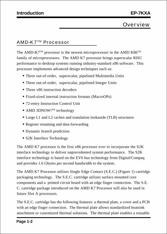
AMD-K7TM Processor
The AMD-K7TM processor is the newest microprocessor in the AMD K86TM
family of microprocessors. The AMD K7 processor brings superscalar RISCperformance to desktop systems running industry-standard x86 software. This
processor implements advanced design techniques such as:
w Three out-of-order, superscalar, pipelined Multimedia Units
w Three out-of-order, superscalar, pipelined Integer Units
w Three x86 instruction decoders
w Fixed-sized internal instruction formats (MacroOPs)
w 72-entry Instruction Control Unit
w AMD 3DNOW!TM technology
w Large L1 and L2 caches and translation lookaside (TLB) structures
w Register renaming and data-forwarding
w Dynamic branch prediction
w S2K Interface Technology
The AMD K7 processor is the first x86 processor ever to incorporate the S2Kinterface technology to deliver unprecedented system performance. The S2K
interface technology is based on the EV6 bus technology from Digital/Compaq
and provides 1.6 Gbytes per second bandwidth to the system.
The AMD K7 Processor utilizes Single Edge Contact (S.E.C.) (Figure 1) cartridge
packaging technology. The S.E.C. cartridge utilizes surface mounted core
components and a printed circuit board with an edge finger connection. The S.E.C. cartridge package introduced on the AMD K7 Processor will also be used in
future Slot A processors.
The S.E.C. cartridge has the following features: a thermal plate, a cover and a PCBwith an edge finger connection. The thermal plate allows standardized heatsink
attachment or customized thermal solutions. The thermal plate enables a reusable

IntroductionEP-7KXA
Page 1-3
heatsink to minimize fit issues for serviceability, upgradeability and replacement.
The full enclosure also protects the surface mount components. The edge fingerconnection maintains socketabilty for system configuration. The edge finger
connector is denoted as ‘Slot A connector’ in this and other documentation.
S.E.C. Cartridge Terminology
• Processor card
The green PCB (with or without components on it)
• Processor core
The CPU silicon chip on the processor card.
• CoverThe plastic cover on the opposite side from the thermal plate.
• Slot A
The slot that the S.E.C. cartridge plugs into.
• Retention mechanismFormerly ‘retention module’ the dual posts, etc. that holds the cartridge in
place.
• Thermal plate
The heatsink attachment plate.
• Heat sink supportsThe support pieces that are mounted on the mainboard to provide added
support for heatsinks.
Figure 1: AMD K7 Processor with S.E.C.C.

Introduction EP-7KXA
Page 1-4
Accelerated Graphics Port(AGP or A.G.P.)
Typically, 3D graphics rendering requires a tremendous amount of memory, and
demands ever increasing throughput speed as well. As 3D products for thepersonal computer become more and more popular, these demands will only
increase. This will cause a rise in costs for both end users and manufacturers.
Lowering these costs as well as improving performance is the primary motivationbehind AGP. By providing a massive increase in the bandwidth available between
the video card and the processor, it will assist in relieving some of these pressures
for quite sometime.
Hardware Monitoring
Hardware monitoring allows you to monitor various aspects of your systems
operations and status. The features include CPU temperature, voltage and RPM of
fan.

IntroductionEP-7KXA
Page 1-5
EP-7KXA Form-Factor
The EP-7KXA is designed with ATX form factor - the new industry standard of
chassis. ATX form factor is essentially a Baby-AT baseboard rotated 90 degreeswithin the chassis enclosure and a new mounting configuration for the power
supply. With these changes the processor is relocated away from the expansion
slots, allowing them all to hold full length add-in cards. ATX defines a doubleheight aperture to the rear of the chassis which can be used to host a wide range of
onboard I/O. Only the size and position of this aperture is defined, allowing PC
manufacturers to add new I/O features (e.g.; TV input, TV output, joystick, modem,LAN, etc.) to systems. This will help systems integrators differentiate their
products in the marketplace, and better meet your needs.
• Smaller size promotes a smaller system size.
• I/O shield does not need to be retooled in an ATX 2.01 or later. The
mainboard should be used in an ATX 2.01 (or later) compliant case.
• A smaller power supply can be used. High integration on mainboardreduces the system costs.
Full lengthslots
Expandable I/O
5 1/4"Bay
3 1/2"Bay
Figure 2: Summary of ATX chassis features
CPU located nearPower Supply
Single chassisfan for system
ATXPowerSupply
ATX power connec-tor
Floppy / IDEconnectorsclose toperipheralbays

Introduction EP-7KXA
Page 1-6
Power-On/Off (Remote)
The EP-7KXA has a single 20-pin connector for ATX power supplies. For ATXpower supplies that support the Remote On/Off feature, this should be connectedto the systems front panel for system Power On/Off button. The systems powerOn/Off button should be a momentary button that is normally open.
The EP-7KXA has been designed with “Soft Off" functions. You can turn Off thesystem from one of two sources: The first is the front panel Power On/Offbutton, and the other is the "Soft Off" function (coming from the EP-7KXA’sonboard circuit controller) that can be controlled by the operating system.Windows 95/98 will control this when the user clicks that they are ready toShutdown the system.
Figure 4: Simple ATX Power ON/OFF Controller
J 3
ATXPOWER SUPPLY
Case (chassis) PowerON/OFF button (J 3)
I/O Shield Connector
The EP-7KXA is equipped with an I/O back panel. Please use the appropriate I/Oshield (figure 3).
Figure 3: I/O back panel layout
PS/2 Mouse
PS/2KEYBOARD
USB port
COM1 COM2
parallel port
SpeakerLine_in
MIC
Joystick/Midi

IntroductionEP-7KXA
Page 1-7
Figure 5: System Block Diagram
System Block Diagram
PACPCI Bridge
and memorycontrollerVT8371
133/100MHz
133/100MHz
66MHz
4X
AMD K7Processor
VT82C686AI/O Bridge
AC97
USB 0,1 USB 2,3
AMR Slot

Introduction EP-7KXA
Page 1-8
Page Left Blank
FeaturesEP-7KXA
Page 2-1
Section 2FEATURES
EP-7KXA Features:
• EP-7KXA is based on the AMD K7 Processor operating at 500 ~ 800MHzon SlotA.
• Designed with VIA KX133 AGPset.
• Supports up to 768MB of DRAM (minimum of 8 MB) on board (pleasesee Section 3-2).
• EP-7KXA will support Error Checking and Correcting (ECC) when using
parity SDRAM memory modules. This will detect multiple bit errors andcorrect 1-bit memory errors.
• Supports (1) 16 bit ISA slots, (5) 32 bit PCI slots, (1) 4X AGP slot, (1) AMRslot and provides (2) independent high performance PCI IDE interfaces
capable of supporting PIO Mode 3/4 and Ultra DMA 33/66 devices.
The EP-7KXA supports (5) PCI Bus Master slots and a jumperless PCIINT# control scheme which reduces configuration confusion when plugging
in PCI card(s).
• Supports ATAPI (e.g. CD-ROM) devices on both Primary and SecondaryIDE interfaces.
• Designed with on chip Multi I/O: (1) floppy port, (1) parallel port (EPP,
ECP), and (2) serial ports (16550 Fast UART).Note: Japanese “Floppy 3 mode” is also supported
• Features Award Plug & Play BIOS. With Flash Memory you can always
upgrade to the current BIOS as they are released.
• EP-7KXA utilizes a Lithium battery which provides environmental
protection and longer battery life.
Features EP-7KXA
Page 2-2
• Supports the (4) Universal Serial Bus (USB) Ports. The onboardVT82C686A chip provides the means for connecting PC peripherals such
as; keyboards, joysticks, telephones, and modems.
• Built-in ATX 20-pin power supply connector.
• Software power-down when using Windows® 95/98.
• Supports ring-in feature (remote power-on through external modem,
allows system to be turned on remotely).
• Resume by Alarm - Allows your system to turn on at a preselected time.
• Power Loss Recovery - In the event of a power outtage your system will
automatically turn itself back on without user intervention.
• Supports CPU Hardware sleep and SMM (System Management Mode).
• Supports Keyboard power ON function (KBPO).
• Built-in WOL (Wake-up On Lan) Connector.
• Built-in WOM (Wake-up On Modem) Connector.
• Built-in AC97 PCI Audio.
• Supports STR (Suspend to RAM) function.

InstallationEP-7KXA
Page 3-1
Section 3INSTALLATION
Installation EP-7KXA
Page 3-2
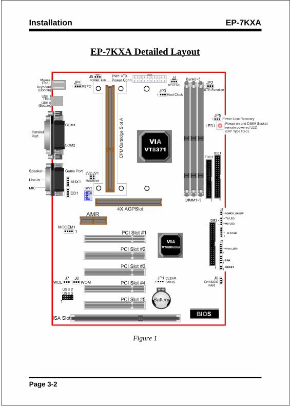
Figure 1
EP-7KXA Detailed Layout

InstallationEP-7KXA
Page 3-3
Easy Installation Procedure
Easy Installation Procedure
The following must be completed before powering on your new system:
3-1. Jumper Settings3-2. System memory Configuration3-3. Install Processor3-4. Device Connectors3-5. External Modem Ring-in Power ON and Keyboard Power ON
Functions (KBPO)3-6. Device Connectors
Section 3-1Jumper Settings
The EP-7KXA motherboard was designed with very few jumpers to make yourinstall fast and easy.
1
JP3: CPU Host Clock Selection
3PJ KCOLCUPC
2-1 zHM001
3-2 zHM331*
12
34
5
ON
SW1: CPU Vcore Voltage Selection
1WS UPCerocV1 2 3 4 5
otuA
NO NO NO V6.1
NO NO NO NO V56.1
NO NO V7.1
NO NO NO V57.1
NO NO NO V8.1
* Reserved
Installation EP-7KXA
Page 3-4
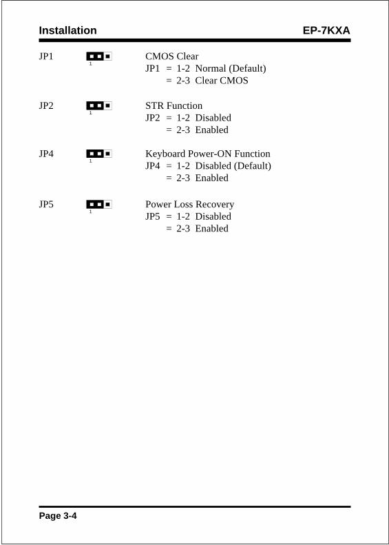
1JP1 CMOS Clear
JP1 = 1-2 Normal (Default)= 2-3 Clear CMOS
1JP5 Power Loss Recovery
JP5 = 1-2 Disabled= 2-3 Enabled
JP4 Keyboard Power-ON FunctionJP4 = 1-2 Disabled (Default)
= 2-3 Enabled
1
1JP2 STR Function
JP2 = 1-2 Disabled= 2-3 Enabled

InstallationEP-7KXA
Page 3-5
Section 3-2System Memory Configuration
Memory LayoutThe EP-7KXA supports (3) PC133 168-pin DIMMs (Dual In-line MemoryModule). The DIMMs can be either SDRAM (Synchronized DRAM) or VCSDRAM (Virtual Channel SDRAM).
• DIMM SDRAM may be 83MHz (12ns), 100MHz (10ns) or125MHz (8ns) bus speed.
• If you use both 50ns and 60ns memory you must configureyour BIOS to read 60ns.
• When using Synchronous DRAM we recommend using the4 clock variety over the 2 clock.
Figure 2 and Table 1 show several possible memory configurations.
* SDRAM only supports 8, 16, 32, 64, 128, 256MB DIMM modules.
* We recommend to use PC100 Memory Module for bus speed between 66MHzand 100MHz and PC133 Memory for bus speed over 100MHz.
* Using non-compliant memory with higher bus speed (over clocking) mayseverely compromise the integrity of the system.
DIMM 1
DIMM 2
B a n k 0 /1
B a n k 2 /3
DIMM 3 B a n k 4 /5
yromeMlatoT1MMID
)1/0knaB(2MMID
)3/2knaB(3MMID
)5/4knaB(
BM652=mumixaM
*MARDS,BM46,BM23,BM61,BM8
1XBM652,BM821enoN enoN
BM215=mumixaM
*MARDS,BM46,BM23,BM61,BM8
1XBM652,BM821
*MARDS,BM46,BM23,BM61,BM8
1XBM652,BM821enoN
BM867=mumixaM
*MARDS,BM46,BM23,BM61,BM8
1XBM652,BM821
*MARDS,BM46,BM23,BM61,BM8
1XBM652,BM821
*MARDS,BM46,BM23,BM61,BM8
1XBM652,BM821
Figure 2
Table 1
Installation EP-7KXA
Page 3-6
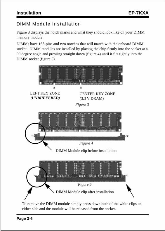
DIMM Module InstallationFigure 3 displays the notch marks and what they should look like on your DIMMmemory module.
DIMMs have 168-pins and two notches that will match with the onboard DIMMsocket. DIMM modules are installed by placing the chip firmly into the socket at a90 degree angle and pressing straight down (figure 4) until it fits tightly into theDIMM socket (figure 5).
Figure 3
Figure 5
DIMM Module clip after installation
To remove the DIMM module simply press down both of the white clips oneither side and the module will be released from the socket.
Figure 4
DIMM Module clip before installation
CENTER KEY ZONE(3.3 V DRAM)
LEFT KEY ZONE(UNBUFFERED)

InstallationEP-7KXA
Page 3-7
Section 3-3Installing Processor
The EP-7KXA uses the Single Edge Contact (SEC) slot for a AMD K7 processor
packaged in an SEC cartridge.
Please have ready the following list of components so that we may install the
processor onto the motherboard.
1. AMD K7 processor heat sink2. AMD K7 Processor
OK, now that you have all of your components ready, we can start.
First, please refer to figure 6 below, and follow the direction to lift up thefoldable AMD K7 Retention Mechanism. This pre-installed device is
designed for you to install AMD K7 CPU more easier and to avoide any
damage on the board due to overtightening the four screws.
One thing must be kept in your mind that please make sure to lift upright
the foldable parts of the Retention module to fit and install CPU properly.
Figure 6
Now we are going to install the heatsink support base piece onto the motherboard.
There is both a large and small hole so that the base will only fit in one direction.
This piece needs to be pushed into the holes firmly until it is seated.
Now we are ready to install the SEC Cartridge (AMD K7 Processor) into the
Retention Module. The SEC Cartridge is mounted by sliding the SEC Cartridge
into the Retention Module and letting it slide all the way down. Once it reachesthe bottom make sure you press firmly on SEC cartridge to firmly secure into the
Slot A Socket.

Installation EP-7KXA
Page 3-8
Section 3-4Device Connectors
Now that your motherboard is installed you are ready to connect all your connec-tions (figure 7).
Figure 7
J2,J3: Chassis Panel Connector• Power_LED, Speaker, Reset, Sleep, Turbo LED and HDD LED
J4: CPU Fan Power• A plug-in for the CPU Fan Power
J5: Power Supply Fan Monitoring• A plug-in for the Power Supply Fan Power
J6: Chassis Fan Power• A plug-in for the chassis Fan Power
J7: WOL (Wake On Lan) Connector
J8: WOM (Wake On Modem) Connector
JV1: Reserved
JV2: Reserved
IDE1: Primary IDE Connector
IDE2: Secondary IDE Connector
FDD1: Floppy Controller Connector
PW1: ATX Power Connector• 20-pin power connector
CD1: CD Audio Connector
AUX1: AUX Audio Connector
MODEM1: Telephony Connector
• Pin1(Audio_in), Pin2/Pin3(GND), Pin4(Mic-out to Modem)
PS/2 Mouse
PS/2KEYBOARD
USB port
COM1 COM2
parallel port
SpeakerLine_in
MIC
Joystic/Midi
InstallationEP-7KXA
Page 3-9
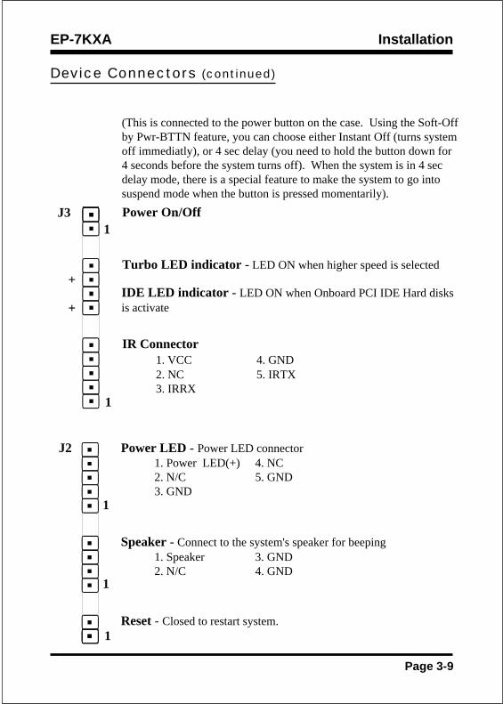
Device Connectors (continued)
(This is connected to the power button on the case. Using the Soft-Offby Pwr-BTTN feature, you can choose either Instant Off (turns systemoff immediatly), or 4 sec delay (you need to hold the button down for4 seconds before the system turns off). When the system is in 4 secdelay mode, there is a special feature to make the system to go intosuspend mode when the button is pressed momentarily).
Turbo LED indicator - LED ON when higher speed is selected
IDE LED indicator - LED ON when Onboard PCI IDE Hard disksis activate
J31
+
+
IR Connector1. VCC 4. GND2. NC 5. IRTX3. IRRX
1
Power On/Off
J2
Speaker - Connect to the system's speaker for beeping1. Speaker 3. GND2. N/C 4. GND
Reset - Closed to restart system.
Power LED - Power LED connector1. Power LED(+) 4. NC2. N/C 5. GND3. GND
1
1
1
Installation EP-7KXA
Page 3-10
Section 3-5External Modem Ring-in PowerON and Keyboard Power ONFunctions (KBPO)
On the basis of bounded functions in I/O chipset, the two serial ports are able to
support the External Modem Ring-in Power ON function. Once users connect theexternal modem to COM1 or COM2, the EP-7KXA mainboard allows users to turn
on their system through the remote and host's dial-up control.
Exclusive Keyboard Power ON Function
To innovate a unique feature to benefit users, we devoted the easiest and mostconvenient way to turn on your system based on the the ATX power supply.
How to work with it
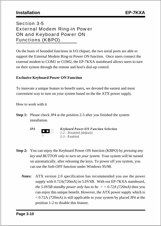
Step 1: Please check JP4 at the position 2-3 after you finished the system
installation.
Step 2: You can enjoy the Keyboard Power ON function (KBPO) by pressing any
key and BUTTON only to turn on your system. Your system will be turned
on automatically, after releasing the keys. To power off you system, youcan use the Soft-OFF function under Windows 95/98.
Notes: ATX version 2.0 specification has recommended you use the powersupply with 0.72A(720mA) in 5.0VSB. With our EP-7KXA mainboard,
the 5.0VSB standby power only has to be > = 0.72A (720mA) then you
can enjoy this unique benefit. However, the ATX power supply which is< 0.72A (720mA) is still applicable to your system by placed JP4 at the
position 1-2 to disable this feature.
JP 4 K eyboard P ow er-O N F un c tion Se lection1-2 : D isab led (defau lt)2 -3 : E n ab led

InstallationEP-7KXA
Page 3-11
3-6 STR (Suspend To RAM) Function
The EP-7KXA supports the STR power management state by maintaining the
appropriate states on the SDRAM interface signals. The power source must bekept alive to the SDRAM during STR (ACPI S3). Advanced Configuration
Power Interface (ACPI) provides more Energy Saving Features for operating
systems that support OS such as Instant ON and QuickStartTM function.
1. To enable the ACPI function and use the STR functionally to save your system
energy, you are recommended to confirm the following requirements:
a. In BIOS, please select “ ACPI function: Enable” and “ACPI Suspend Type:S3(STR)” in the Power Management Setup menu.
b. Then, please type the following before installing the Windows® 98:
{Driver}:> Setup /p j
If the Windows® 98 installed in your system without the parameters above,please do refer your manual or contact Microsoft for more detail and then
upgrade the system to support ACPI function.
c. Restart your system.
d. Getting in to the “Advanced” of the Power Management icon of Control
Panel, and selecting the “Stand By” in the Power Buttons.
2. Getting start with STR function, please click the START button and choose
Shut Down icon. Then, select the Stand By option in the Shut Down Windows
box to let system go to STR mode.
Here are the differences between STR power saving mode and Green (or
Suspend) mode:
a. It is the most advanced Power Management mode
b. It cuts all the power supplied to peripherals except to Memory - max. powersaving
Installation EP-7KXA
Page 3-12
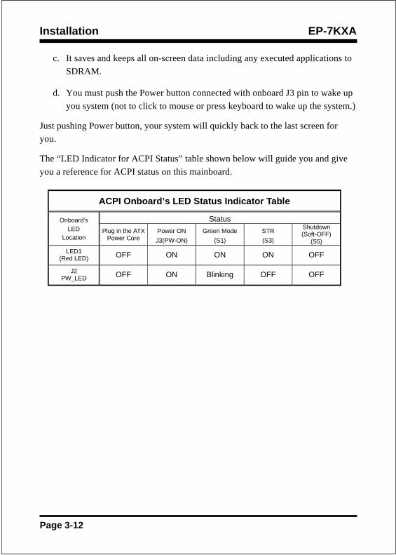
ACPI Onboard’s LED Status Indicator Table
StatusOnboard’sLED
LocationPlug in the ATX
Power CorePower ON
J3(PW-ON)
Green Mode
(S1)
STR
(S3)
Shutdown(Soft-OFF)
(S5)
LED1(Red LED) OFF ON ON ON OFF
J2PW_LED OFF ON Blinking OFF OFF
c. It saves and keeps all on-screen data including any executed applications to
SDRAM.
d. You must push the Power button connected with onboard J3 pin to wake up
you system (not to click to mouse or press keyboard to wake up the system.)
Just pushing Power button, your system will quickly back to the last screen foryou.
The “LED Indicator for ACPI Status” table shown below will guide you and give
you a reference for ACPI status on this mainboard.

BIOSEP-7KXA
Page 4-1
Section 4AWARD BIOS SETUP
Main Menu
Award’s ROM BIOS provides a built-in Setup program which allows user tomodify the basic system configuration and hardware parameters. The modifieddata will be stored in a battery-backed CMOS, so that data will be retained evenwhen the power is turned off. In general, the information saved in the CMOSRAM will stay unchanged unless there is a configuration change in the system,such as hard drive replacement or a device is added.
It is possible for the CMOS battery to fail, this will cause data loss in the CMOSonly. If this does happen you will need to reconfigure your BIOS settings.
To enter the Setup Program :
Power on the computer and press the <Del> key immediately, this will bring youinto the BIOS CMOS SETUP UTILITY.
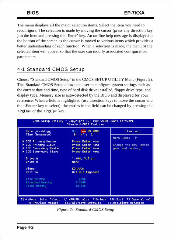
Figure 1: CMOS Setup Utility
BIOS EP-7KXA
Page 4-2
The menu displays all the major selection items. Select the item you need toreconfigure. The selection is made by moving the cursor (press any direction key) to the item and pressing the ‘Enter’ key. An on-line help message is displayed atthe bottom of the screen as the cursor is moved to various items which provides abetter understanding of each function. When a selection is made, the menu of theselected item will appear so that the user can modify associated configurationparameters.
4-1 Standard CMOS Setup
Choose “Standard CMOS Setup” in the CMOS SETUP UTILITY Menu (Figure 2).The Standard CMOS Setup allows the user to configure system settings such asthe current date and time, type of hard disk drive installed, floppy drive type, anddisplay type. Memory size is auto-detected by the BIOS and displayed for yourreference. When a field is highlighted (use direction keys to move the cursor andthe <Enter> key to select), the entries in the field can be changed by pressing the<PgDn> or the <PgUp> key.
Figure 2: Standard CMOS Setup

BIOSEP-7KXA
Page 4-3
NOTE: If the hard disk Primary Master/Slave and Secondary Master/Slave are set to Auto, then the hard disk size and model will be auto-detected.NOTE: The “Halt On:” field is used to determine when to halt the systemby the BIOS if an error occurs.NOTE: Floppy 3 Mode support is a mode used to support a special 3.5”drive used in Japan. This is a 3.5” disk that stores only 1.2 MB, thedefault setting for this is disabled.
4-2 Advanced BIOS Features
Selecting the “BIOS FEATURES SETUP” option in the CMOS SETUP UTILITYmenu allows users to change system related parameters in the displayed menu.This menu shows all of the manufacturer’s default values for the EP-7KXA.
Pressing the [F1] key will display a help message for the selected item.
Figure 3: BIOS Features Setup
BIOS EP-7KXA
Page 4-4
Virus Warning : During and after the system boots up, any attempt to write to theboot sector or partition table of the hard disk drive will halt the system and anerror message will appear.
You should then run an anti-virus program to locate the virus. Keep in mind thatthis feature protects only the boot sector, not the entire hard drive.The default value is Disabled.
Enabled: Activates automatically when the system boots up causing a warningmessage to appear when anything attempts to access the boot sector.
Disabled: No warning message will appear when anything attempts to access theboot sector.
Note:Many disk diagnostic programs that access the boot sector tablecan trigger the virus warning message. If you plan to run such aprogram, we recommend that you first disable the virus warning.
CPU Internal Cache: This controls the status of the processor’s internal cachearea. The default is Enabled.Enabled: This activates the processor’s internal cache thereby increasing
performance.Disabled: This deactivates the processor’s internal cache thereby lowering
performance.
External (L2) Cache: This controls the status of the external (L2) cache area.The default is Enabled.Enabled: This activates the motherboard’s L2 cache thereby increasing
performance.Disabled: This deactivates the motherboard’s L2 cache thereby lowering
performance.
CPU L2 Cache ECC Checking: This control if the CPU’s L2 Cache willsupport Error Checking and Correcting (ECC). The default is Disabled.Enabled: Enables ECC support for the CPU’s L2 cache. Performance will
decrease 2% ~ 4%.Disabled: Disables ECC support for the CPU’s L2 cache.
Quick Power On Self Test: This category speeds up the Power On Self Test(POST). The default is Enabled.Enabled: This setting will shorten or skip of the items checked during POST.Disabled: Normal POST.
BIOSEP-7KXA
Page 4-5
First /Second/Third/Other Boot Device: The BIOS attempts to load the operat-
ing system from the devices in the sequence selected in these items.
The choice: Floppy, LS/ZIP, HDD, SCSI, CDROM, Disabled.
Swap Floppy Drive: This will swap your physical drive letters A & B if you are
using two floppy disks. The default is Disabled.Enabled: Floppy A & B will be swapped under the O/S.
Disabled: Floppy A & B will be not swapped.
Boot Up Floppy Seek: During Power-On-Self-Test (POST), BIOS will deter-
mine if the floppy disk drive installed is 40 or 80 tracks. Only 360K type is 40
tracks while 760K, 1.2MB and 1.44MB are all 80 tracks. The default is Enabled.Enabled: The BIOS will search the floppy disk drive to determine if it is 40 or
80 tracks.
Disabled: The BIOS will not search for the type of floppy disk drive by tracknumber.
Note: BIOS can not tell the difference between 720K, 1.2MB and 1.44MBdrive types as they are all 80 tracks.
Boot Up NumLock Status: This controls the state of the NumLock key when thesystem boots. The default is On.
On: The keypad acts as a 10-key pad.
Off : The keypad acts like the cursor keys.
Gate A20 Option: This refers to the way the system addresses memory above1MB (extended memory). The default is Fast.
Normal : The A20 signal is controlled by the keyboard controller or chipset
hardware.Fast: The A20 signal is controlled by Port 92 or chipset specific method.
Typematic Rate Setting: This determines the keystrokes repeat rate.The default is Disabled.
Enabled: Allows typematic rate and typematic delay programming.
Disabled: The typematic rate and typematic delay will be controlled by thekeyboard controller in your system.
BIOS EP-7KXA
Page 4-6
Typematic Rate (Chars/Sec): This is the number of characters that will be
repeated by a keyboard press. The default is 6.6: 6 characters per second. 8: 8 characters per second.10: 10 characters per second. 12: 12 characters per second.15: 15 characters per second. 20: 20 characters per second.24: 24 characters per second. 30: 30 characters per second.
Typematic Delay (msec): This setting controls the time between the first andthe second character displayed by typematic auto-repeat. The default is 250.
250: 250 msec.500: 500 msec.750: 750 msec.1000: 1000 msec.
Security Option: This category allows you to limit access to the System andSetup, or just to Setup. The default is Setup.System: The system will not boot and the access to Setup will be denied if the
correct password is not entered at the prompt.Setup: The system will boot; but the access to Setup will be denied if the
incorrect password is not entered at the prompt.
OS Select For DRAM > 64MB: Some operating systems require specialhandling. Use this option only if your system has greater than 64MB of memory.The default is Non-OS2.OS2: Select this if you are running the OS/2 operating system with greater
than 64MB of RAM.Non-OS2: Select this for all other operating systems and configurations.
Video BIOS Shadow: This option allows video BIOS to be copied into RAM.Video Shadowing will increase the video performance of your system.The default is Enabled.Enabled: Video shadow is enabled.Disabled: Video shadow is disabled.
C8000 - CBFFF Shadow:CC000 - CFFFF Shadow:D0000 - D3FFF Shadow:D4000 - D7FFF Shadow:

BIOSEP-7KXA
Page 4-7
D8000 - DBFFF Shadow:
DC000 - DFFFF Shadow:
These categories determine whether ROMs from option cards will be copied intoRAM. This will be in 16K byte or 32K byte units, and the size will depend onchipset of the option card.
Enabled: Optional shadow is enabled.Disabled: Optional shadow is disabled.

BIOS EP-7KXA
Page 4-8
Bank 0/1, 2/3, 4/5 DRAM Timing: This value in this field is set by the systemboard manufacturer, depending on whether the board has paged DRAMs or EDO(extended data output) DRAMs.The Choice: Bank 0/1, 2/3, 4/5.
SDRAM Cycle length: This setting defines the CAS timing parameter of theSDRAM in terms of clocks. The default is 3.2: Provides faster memory performance.3: Provides better memory compatibility.
Bank Interleave: The item allows you to set how many banks of SDRAM supportin your mainboard.The Choice: 2 Bank, 4 Bank, Disabled.
4-3 Advanced Chipset Features
Choose the “CHIPSET FEATURES SETUP” in the CMOS SETUP UTILITY menuto display following menu.
Figure 4: Chipset Features Setup

BIOSEP-7KXA
Page 4-9
DRAM Page-Mode: The item will active or inactive chipset page registers.Enabled: Page-Mode Enabled.Disabled: No page registers update and non Page-Mode operation.
Memory Hole : You can reserve this memory area for the use of ISA adaptorROMs. The default is Disabled.Enabled: This field enables the main memory (15~16MB) to remap to ISA BUS.Disabled:Normal Setting. Note: If this feature is enabled you will not be able to cache this memory segment.
System BIOS Cacheable: This allows you to copy your BIOS code from slowROM to fast RAM. The default is Disabled.Enabled: The option will improve system performance. However, if any program
writes to this memory area, a system error may result.Disabled: System BIOS non-cacheable.
Video BIOS Cacheable: This option copies the video ROM BIOS to fast RAM(C0000h to C7FFFh). The default is Enabled.Enabled: Enables the Video BIOS Cacheable to speed up the VGA Performance.Disabled: Will not use the Video BIOS Cacheable function.
Video RAM Cacheable: This option allows the CPU to cache read/writes of thevideo RAM. The default is Enabled.Enabled: This option allows for faster video access.Disabled: Reduced video performance.
AGP Aperture Size: The amount of system memory that the AGP card isallowed to share. The default is 64.
4: 4MB of systems memory accessable by the AGP card.
8: 8MB of systems memory accessable by the AGP card.
16: 16MB of systems memory accessable by the AGP card.
32: 32MB of systems memory accessable by the AGP card.
64: 64MB of systems memory accessable by the AGP card.
128: 128MB of systems memory accessable by the AGP card.
256: 256MB of systems memory accessable by the AGP card.

BIOS EP-7KXA
Page 4-10
AGP-4X Mode: Chipset AGP Mode support.Options: x1 , x2 and x4.
USB Keyboard Support: This controls the activation status of an optional USBkeyboard that may be attached. The default is disabled.Enabled: Enable USB keyboard support.Disabled: Disable USB keyboard support.
OnChip Sound: Turn on/off onchip sound device.
OnChip Modem: Turn on/off onchip software modem device.
CPU to PCI Write Buffer : When enabled, up to four D words of data can bewritten to the PCI bus without interruting the CPU. When disabled, a write bufferis not used and the CPU read cycle will not be completed until the PCI bus signalsthat it is ready to receive the data.The Choice: Enabled, Disabled.
PCI Dynamic Bursting: When Enabled, data transfers on the PCI bus, wherepossible, make use of the high-performance PCI bust protocol, in which graeateramounts of data are transferred at a single command.The Choice: Enabled, Disabled.
PCI Master 0 WS Write: When Enabled, writes to the PCI bus are commandwith zero wait states.The Choice: Enabled, Disabled.
PCI Delay Transaction: The chipset has an embedded 32-bit posted write bufferto support delay transactions cycles. Select Enabled to support compliance withPCI specification version 2.1.The Choice: Enabled, Disabled.
PCI #2 Access #1 Retry: This item allows you enabled/disable the PCI #2Access #1 Retry.The Choice: Enabled, Disabled.
Memory Parity/ECC Check: If the DRAM chip in your system support Parity/ECC check, select Enabled.

BIOSEP-7KXA
Page 4-11
4-4 Integrated Peripherals
Figure 5: Integrated Peripherals
Note: If you do not use the Onboard IDE connector, then you will need toset Onboard Primary PCI IDE: Disabled and Onboard SecondaryPCI IDE: Disabled
Note: The Onboard PCI IDE cable should be equal to or less than 18inches (45 cm.).
OnChip IDE Channel0: The default value is Enabled.Enabled: Enables Onboard IDE primary port.Disabled: Disables Onboard IDE primary port.
OnChip IDE Channel1: The default is Enabled.Enabled: Enables Onboard IDE secondary port.Disabled: Disables Onboard IDE secondary port.
IDE Prefetch Mode: Enable prefetching for IDE drive interfaces that support itsfaster drive accesses. If uou are getting disk drive errors, change the setting toomit the drive interface where the errors occur. Depending on the configuration

BIOS EP-7KXA
Page 4-12
of your IDE subsystem, this field may not appear, and it does not appear when theInternal PCI/IDE field, above, is Disabled.The Choice: Enabled, Disabled.
Primary Master PIO: The default is Auto.Auto: BIOS will automatically detect the Onboard Primary Master PCI IDE
HDD Accessing mode.Mode 0~4: Manually set the IDE Programmed interrupt mode.
Primary Slave PIO: The default is Auto.Auto: BIOS will automatically detect the Onboard Primary Slave PCI IDE
HDD Accessing mode.Mode 0~4: Manually set the IDE Programmed interrupt mode.
Secondary Master PIO: The default is Auto.Auto: BIOS will automatically detect the Onboard Secondary Master PCI
IDE HDD Accessing mode.Mode 0~4: Manually set the IDE Programmed interrupt mode.
Secondary Slave PIO: The default is Auto.Auto: BIOS will automatically detect the Onboard Secondary Slave PCI
IDE HDD Accessing mode.Mode 0~4: Manually set the IDE Programmed interrupt mode.
Primary Master UDMA : This allows you to select the mode of operation forthe hard drive. The default is Auto.Auto: The computer will select the optimal setting.Disabled: The hard drive will run in normal mode.
Primary Slave UDMA: This allows you to select the mode of operation for thehard drive. The default is Auto.Auto: The computer will select the optimal setting.Disabled: The hard drive will run in normal mode.
Secondary Master UDMA: This allows you to select the mode of operation forthe hard drive. The default is Auto.Auto: The computer will select the optimal setting.Disabled: The hard drive will run in normal mode.

BIOSEP-7KXA
Page 4-13
Secondary Slave UDMA: This allows you to select the mode of operation forthe hard drive. The default is Auto.Auto: The computer will select the optimal setting.Disabled: The hard drive will run in normal mode.
Init Display First: If two video cards are used (1 AGP and 1 PCI) this specifieswhich one will be the primary display adapter. The default is PCI Slot.PCI Slots: PCI video card will be primary adapter.AGP: AGP video card will be primary adapter.
IDE HDD Block Mode: IDE Block Mode allows the controller to access blocksof sectors rather than a single sector at a time. The default is Enabled.Enabled: Enabled IDE HDD Block Mode. Provides higher HDD transfer rates.Disabled: Disable IDE HDD Block Mode.
Onboard FDD Controller : This controls the state of the onboard floppycontroller. The default value is Enabled.Enabled: Enable the Onboard VIA686A Chips’s floppy drive interface controller.Disabled: Disable the Onboard VIA686A Chip’s floppy drive interface controller.
Onboard Serial Port 1: This field allows the user to configure the 1st serialport. The default is Auto.
AUTO : Enable Onboard Serial port 1 and address is Auto adjusted.
COM1: Enable Onboard Serial port 1 and address is 3F8H/IRQ4.
COM2: Enable Onboard Serial port 1 and address is 2F8H/IRQ3.
COM3: Enable Onboard Serial port 1 and address is 3E8H/IRQ4.
COM4: Enable Onboard Serial port 1 and address is 2E8H/IRQ3.
Disabled: Disable Onboard SMC CHIP’s Serial port 1.
Onboard Serial Port 2: This field allows the user to configure the 2nd serial port.The default is Auto.
AUTO : Enable Onboard Serial port 2 and address is Auto adjusted.
COM1: Enable Onboard Serial port 2 and address is Auto.
COM2: Enable Onboard Serial port 2 and address is 2F8H/IRQ3.
COM3: Enable Onboard Serial port 2 and address is 3E8H/IRQ4.
COM4: Enable Onboard Serial port 2 and address is 2E8H/IRQ3.
Disabled: Disable Onboard SMC CHIP’s Serial port 2.

BIOS EP-7KXA
Page 4-14
UART 2 Mode: This item allows you to determine which Infra Red (IR) functionof onboard I/O chip.The Choice: Standard, ASKIR, HPSIR.
Onboard Parallel port: This field allows the user to configure the LPT port.The default is 378H / IRQ7.378H: Enable Onboard LPT port and address is 378H and IRQ7.278H: Enable Onboard LPT port and address is 278H and IRQ5.3BCH: Enable Onboard LPT port and address is 3BCH and IRQ7.Disabled: Disable Onboard Winbond Chip’s LPT port.
Onboard Parallel Port Mode: This field allows the user to select the parallelport mode.The default is Normal.Normal: Standard mode. IBM PC/AT Compatible bidirectional parallel port.EPP: Enhanced Parallel Port mode.ECP: Extended Capabilities Port mode.EPP+ECP: ECP Mode & EPP Mode.
Onboard Legacy Audio: Legacy Audio enabled/disabled.
Sound Blaster: Sound Blaster compatible device enabled/disabled.
SB I/O Base Address: Sound Blaster I/O resource selection.
SB IRQ Select: Legacy audio device IRQ selection.
SB DMA Select: Sound Blaster DMA channel selection.
MPU-401: MPU-401 function enabled/disabled.
MPU-401 I/O Address: Built-in MPU-401 compatible MIDI I/O port selection:300-303H310-313H320-323H330-333H (default)
Game Port (200-207H): Built-in joystick port support disabled/enabled(default).

BIOSEP-7KXA
Page 4-15
4-5 Power Management Setup
Choose the “POWER MANAGEMENT SETUP” in the CMOS SETUP UTILITY todisplay the following screen. This menu allows the user to modify the powermanagement parameters and IRQ signals. In general, these parameters should notbe changed unless it’s absolutely necessary.
Figure 6: Power Management Setup
ACPI Function : This option allows you to select ACPI Function.The default is Enabled.Enabled: Support ACPI function for new O.SDisabled: No Support ACPI function.
You can only change the content of Doze Mode, Standby Mode, and SuspendMode when the Power Management is set to ‘User Define’.
Power Management: Use this to select your Power Management selection.The default is User define.
Disabled: The system operates in NORMAL conditions (Non-GREEN), andthe Power Management function is disabled.
Max. saving: Maximum power savings. Inactivity period is 1 minute in each mode.

BIOS EP-7KXA
Page 4-16
Min. saving: Minimum power savings. Inactivity period is 1 hour in each mode.
User define: Allows user to define PM Timers parameters to control powersaving mode.
ACPI Suspend Type: This item allows you to select S1(POS) or S3(STR) function.The choice: S1(POS), S3(STR).
PM controlled APM : This option shows weather or not you want the PowerManagement to be controlled the Advanced Power Management (APM).The default is Yes.Yes: APM controls your PMNo: APM does not control your PM
Video Off Option: Tells you what time frame that the video will be disabledunder current power management settings. The default is Standby.Standby: Video powers off after time shown in standby mode setting.Doze: Video powers off after time shown in doze mode setting.Suspend: Video powers off after time shown in suspend mode setting.N/A: Video power off not controlled by power management.
Video Off Method: This option allows you to select how the video will bedisabled by the power management. The default is V/H Sync + Blank
V/H Sync + Blank: System turns off vertical and horizontal synchronizationports and writes blanks to the video buffer.
DPMS: Select this option if your monitor supports the DisplayPower Management Signaling (DPMS) standard of theVideo Electronics Standards Association (VESA). Use thesoftware supplied for your video subsystem to select videopower management values.
Blank Screen: System only writes blanks to the video buffer.
MODEM Use IRQ: Name the interrupt request (IRQ) line assigned to themodem (if any) on your system. Activity of the selected IRQ always awakens thesystem. Default is IRQ 3.N/A: No IRQ is used. 3: IRQ 34: IRQ 4 5: IRQ 57: IRQ 7 9: IRQ 910: IRQ 10 11: IRQ 11

BIOSEP-7KXA
Page 4-17
Soft-Off by PWRBTN: Use this to select your soft-off function.The default is Delay 4 sec.Instant Off : Turns off the system instantly.
Delay 4 Second : Turns off the system after a 4 second delay. If momentarypress of button, the system will go into Suspend Mode. Pressthe power botton again to take system out of Suspend Mode.
State After Power Failure: This field lets you determine the state that your PCreturns to after a power failure. If set to Off, the PC will not boot after a powerfailure, if set to On, the PC will restart after a power failure.
CPU FAN In Suspend: This option is used to set if the CPU fans will turn offduring suspend mode. The default is Off.On: The system will turn off the CPU fans during suspend mode.Off: The system will not turn off the CPU fan during suspend mode.
VGA: When set to On (default), any event occurring at a VGA port will awaken asystem which has been powered down.
LPT & COM: When set to On (default), any event occurring at a COM(serial)/LPT (printer) port will awaken a system which has been powered down.
HDD & FDD : When set to On (default), any event occurring at a hard or floppydrive port will awaken a system which has been powered down.
PCI Card : When set to On (default), any event occurring to the DMA controllerwill awaken a system which has been powered down.
Modem Ring Resume: When set to Enabled, any event occurring to the ModemRing will awaken a system which has been powered down.
RTC Alarm Resume: When set to Enable rtc alarm resume, you could set thedate (of month) and timer (hh:mm:ss), any event occurring at will awaken asystem which has been powered down.
Primary INTR : When set to On (default), any event occurring at will awaken asystem which has been powered down.
BIOS EP-7KXA
Page 4-18
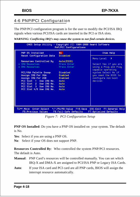
4-6 PNP/PCI Configuration
The PNP/PCI configuration program is for the user to modify the PCI/ISA IRQsignals when various PCI/ISA cards are inserted in the PCI or ISA slots.
WARNING: Conflicting IRQ’s may cause the system to not find certain devices.
Figure 7: PCI Configuration Setup
PNP OS Installed: Do you have a PNP OS installed on your system. The defaultis No.
Yes: Select if you are using a PNP OS.No: Select if your OS does not support PNP.
Resources Controlled By: Who controlled the system PNP/PCI resources.The default is Auto.
Manual: PNP Card’s resources will be controlled manually. You can set whichIRQ-X and DMA-X are assigned to PCI/ISA PNP or Legacy ISA Cards.
Auto: If your ISA card and PCI card are all PNP cards, BIOS will assign theinterrupt resource automatically.
BIOSEP-7KXA
Page 4-19
Reset Configuration Data: This setting allows you to clear ESCD data.The default is DisabledDisabled: Normal Setting.Enabled: If you have plugged in some Legacy cards to the system and they were
recorded into ESCD (Extended System Configuration Data), you canset this field to Enabled in order to clear ESCD.
PCI/VGA Palette Snoop: Leave this field at Disabled.The choice: Enabled, Disabled.
Slot 1 to Slot 5 Use IRQ No: These settings allow the user to specify what IRQwill be assigned to PCI devices in the chosen slot. Options available: Auto,3,4,5,7,9,10,11,12,14 & 15. The defaults are Auto.
BIOS EP-7KXA
Page 4-20
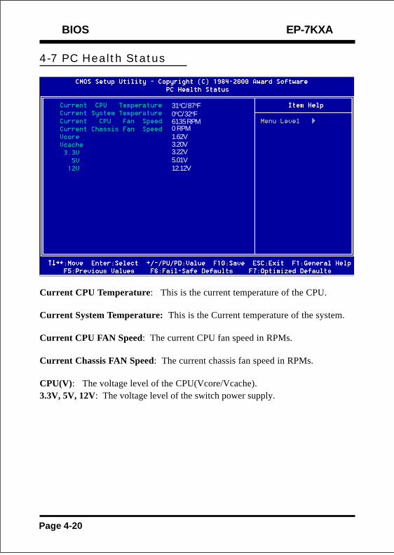
4-7 PC Health Status
Current CPU Temperature: This is the current temperature of the CPU.
Current System Temperature: This is the Current temperature of the system.
Current CPU FAN Speed: The current CPU fan speed in RPMs.
Current Chassis FAN Speed: The current chassis fan speed in RPMs.
CPU(V): The voltage level of the CPU(Vcore/Vcache).3.3V, 5V, 12V: The voltage level of the switch power supply.
31oC/87oF0oC/32oF6135 RPM0 RPM1.62V3.20V3.22V5.01V12.12V

BIOSEP-7KXA
Page 4-21
4-8 Frequency/Voltage Control
Auto Detect DIMM/PCI Clk : When enabled the motherboard will automaticallydisable the clock source for a DIMM socket which does not have a module in it.Same applies for PCI slots. The default is Enabled.
Enabled: Enables this option.Disabled: Disables this option.
CPU Host Clock (CPU/PCI): Allows the external clock to be modifieddepending upon what FSB has been selected. Should not be used to clock proces-sor faster than it was designed for. The default is Default.
100/133 Spread Spectrum : The default is Enabled.Enabled: Enables this option.Disabled: Disables this option.
DRAM Clock : The item will synchronize/asynchronize DRAM operation clock.Host Clock: DRAM has same working clock with CPU host bus.2/3 Host: DRAM running with lower operation clock.
BIOS EP-7KXA
Page 4-22
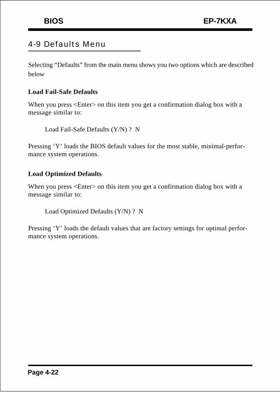
4-9 Defaults Menu
Selecting “Defaults” from the main menu shows you two options which are described
below
Load Fail-Safe Defaults
When you press <Enter> on this item you get a confirmation dialog box with amessage similar to:
Load Fail-Safe Defaults (Y/N) ? N
Pressing ‘Y’ loads the BIOS default values for the most stable, minimal-perfor-mance system operations.
Load Optimized Defaults
When you press <Enter> on this item you get a confirmation dialog box with amessage similar to:
Load Optimized Defaults (Y/N) ? N
Pressing ‘Y’ loads the default values that are factory settings for optimal perfor-mance system operations.

BIOSEP-7KXA
Page 4-23
4-10 Supervisor/User Password Setting
You can set either supervisor or user password, or both of then. The differences
between are:
supervisor password : can enter and change the options of the setup menus.user password : just can only enter but do not have the right to change the
options of the setup menus. When you select this function, the following message
will appear at the center of the screen to assist you in creating a password.
ENTER PASSWORD:
Type the password, up to eight characters in length, and press <Enter>. The pass-
word typed now will clear any previously entered password from CMOS memory.
You will be asked to confirm the password. Type the password again and press<Enter>. You may also press <Esc> to abort the selection and not enter a password.
To disable a password, just press <Enter> when you are prompted to enter the
password. A message will confirm the password will be disabled. Once the pass-word is disabled, the system will boot and you can enter Setup freely.
PASSWORD DISABLED.
When a password has been enabled, you will be prompted to enter it every time you
try to enter Setup. This prevents an unauthorized person from changing any part ofyour system configuration.
Additionally, when a password is enabled, you can also require the BIOS to request
a password every time your system is rebooted. This would prevent unauthorizeduse of your computer.
You determine when the password is required within the BIOS Features Setup Menu
and its Security option (see Section 3). If the Security option is set to “System”, thepassword will be required both at boot and at entry to Setup. If set to “Setup”,
prompting only occurs when trying to enter Setup.
BIOS EP-7KXA
Page 4-24
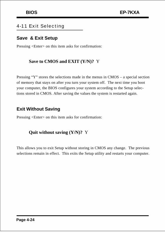
4-11 Exit Selecting
Save & Exit Setup
Pressing <Enter> on this item asks for confirmation:
Save to CMOS and EXIT (Y/N)? Y
Pressing “Y” stores the selections made in the menus in CMOS – a special section
of memory that stays on after you turn your system off. The next time you bootyour computer, the BIOS configures your system according to the Setup selec-
tions stored in CMOS. After saving the values the system is restarted again.
Exit Without Saving
Pressing <Enter> on this item asks for confirmation:
Quit without saving (Y/N)? Y
This allows you to exit Setup without storing in CMOS any change. The previous
selections remain in effect. This exits the Setup utility and restarts your computer.

Appendix
A-1
EP-7KXA
Appendix A
A-1 MEMORY MAPAddress Range Size Description[00000-7FFFF] 512K Conventional memory[80000-9FBFF] 127K Extended Conventional memory[9FC00-9FFFF] 1K Extended BIOS data area if PS/2 mouse is
installed[A0000-C7FFF] 160K Available for Hi DOS memory[C8000-DFFFF] 96K Available for Hi DOS memory and adapter
ROMs[E0000-EEFFF] 60K Available for UMB[EF000-EFFFF] 4K Video service routine for Monochrome &
CGA adaptor[F0000-F7FFF] 32K BIOS CMOS setup utility[F8000-FCFFF] 20K BIOS runtime service routine (2)[FD000-FDFFF] 4K Plug and Play ESCD data area[FE000-FFFFF] 8K BIOS runtime service routine (1)
A-2 I/O MAP[000-01F] DMA controller.(Master)[020-021] INTERRUPT CONTROLLER.(Master)[022-023] CHIPSET control registers. I/O ports.[040-05F] TIMER control registers.[060-06F] KEYBOARD interface controller.(8042)[070-07F] RTC ports & CMOS I/O ports.[080-09F] DMA register.[0A0-0BF] INTERRUPT controller.(Slave)[0C0-0DF] DMA controller.(Slave)[0F0-0FF] MATH COPROCESSOR.[1F0-1F8 ] HARD DISK controller.[278-27F] PARALLEL port 2.[2B0-2DF] GRAPHICS adapter controller.

Appendix EP-7KXA
A-2
[2F8-2FF] SERIAL port 2.[360-36F] NETWORK ports.[378-37F] PARALLEL port 1.[3B0-3BF] MONOCHROME & PARALLEL port adapter.[3C0-3CF] EGA adapter.[3D0-3DF] CGA adapter.[3F0-3F7] FLOPPY DISK controller.[3F8-3FF] SERIAL port 1.
A-3 TIMER & DMA CHANNELS MAPTIMER MAP:TIMER Channel 0 System timer interrupt.TIMER Channel 1 DRAM REFRESH request.TIMER Channel 2 SPEAKER tone generator.DMA CHANNELS:DMA Channel 0 Available.DMA Channel 1 Onboard ECP (Option).DMA Channel 2 FLOPPY DISK (SMC CHIP).DMA Channel 3 Onboard ECP (default).DMA Channel 4 Cascade for DMA controller 1.DMA Channel 5 Available.DMA Channel 6 Available.DMA Channel 7 Available
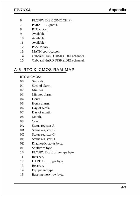
A-4 INTERRUPT MAPNMI :Parity check error.IRQ (H/W):0 System TIMER interrupt from TIMER 0.1 KEYBOARD output buffer full.2 Cascade for IRQ 8-15.3 SERIAL port 2.4 SERIAL port 1.5 PARALLEL port 2.
Appendix
A-3
EP-7KXA
6 FLOPPY DISK (SMC CHIP).7 PARALLEL port 1.8 RTC clock.9 Available.10 Available.11 Available.12 PS/2 Mouse.13 MATH coprocessor.14 Onboard HARD DISK (IDE1) channel.15 Onboard HARD DISK (IDE1) channel.
A-5 RTC & CMOS RAM MAPRTC & CMOS:00 Seconds.01 Second alarm.02 Minutes.03 Minutes alarm.04 Hours.05 Hours alarm.06 Day of week.07 Day of month.08 Month.09 Year.0A Status register A.0B Status register B.0C Status register C.0D Status register D.0E Diagnostic status byte.0F Shutdown byte.10 FLOPPY DISK drive type byte.11 Reserve.12 HARD DISK type byte.13 Reserve.14 Equipment type.15 Base memory low byte.

Appendix EP-7KXA
A-4
16 Base memory high byte.17 Extension memory low byte.18 Extension memory high byte.19-2d2E-2F30 Reserved for extension memory low byte.31 Reserved for extension memory high byte.32 DATE CENTURY byte.33 INFORMATION FLAG.34-3F Reserve.40-7F Reserved for CHIPSET SETTING DATA.

Appendix
A-5
EP-7KXA
Appendix B
B-1 POST CODES
For BIOS 6.0 Code
POST (hex) DESCRIPTIONCFh Test CMOS R/W functionality.C0h Early chipset initialization:
- Disable shadow RAM- Disable L2 cache (socket 7 or below)- Program basic chipset registers
C1h Detect memory- Auto-detection of DRAM size, type and ECC.- Auto-detection of L2 cache (socket 7 or below)
C3h Expand compressed BIOS code to DRAM C5h Call chipset hook to copy BIOS back to E000 & F000
shadow RAM. 0h1 Expand the Xgroup codes locating in physical address
1000:0 02h Reserved 03h Initial Superio_Early_Init switch. 04h Reserved 05h 1. Blank out screen
2. Clear CMOS error flag 06h Reserved 07h 1. Clear 8042 interface
2. Initialize 8042 self-test 08h 1. Test special keyboard controller for Winbond 977
series Super I/O chips.2. Enable keyboard interface.
09h Reserved 0Ah 1. Disable PS/2 mouse interface (optional).
2. Auto detect ports for keyboard & mouse followed bya port & interface swap (optional).

Appendix EP-7KXA
A-6
3. Reset keyboard for Winbond 977 series Super I/Ochips.
0Ch Reserved0Dh Reserved0Eh Test F000h segment shadow to see whether it is R/W-
able or not. If test fails, keep beeping the speaker.0Fh Reserved10h Auto detect flash type to load appropriate flash R/W
codes into the run time area in F000 for ESCD & DMIsupport.
11h Reserved12h Use walking 1’s algorithm to check out interface in
CMOS circuitry. Also set real-time clock power status,and then check for override.
13h Reserved14h Program chipset default values into chipset. Chipset
default values are MODBINable by OEM customers.15h Reserved16h Initial Early_Init_Onboard_Generator switch.17h Reserved18h Detect CPU information including brand, SMI type
(Cyrix or Intel) and CPU level (586 or 686).19h Reserved1Ah Reserved1Bh Initial interrupts vector table. If no special specified, all
H/W interrupts are directed to PURIOUS_INT_HDLR& S/W interrupts to SPURIOUS_soft_HDLR.
1Ch Reserved1Dh Initial EARLY_PM_INIT switch.1Eh Reserved1Fh Load keyboard matrix (notebook platform)20h Reserved21h HPM initialization (notebook platform)22h Reserved23h 1. Check validity of RTC value: e.g. a value of 5Ah is an
invalid value for RTC minute.2. Load CMOS settings into BIOS stack. If CMOS
checksum fails, use default value instead.
Appendix
A-7
EP-7KXA
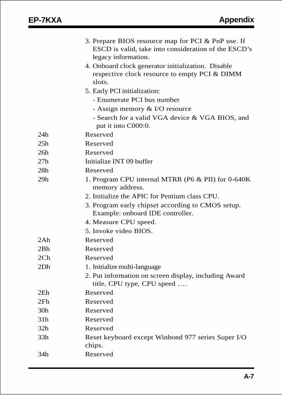
3. Prepare BIOS resource map for PCI & PnP use. IfESCD is valid, take into consideration of the ESCD’slegacy information.
4. Onboard clock generator initialization. Disablerespective clock resource to empty PCI & DIMMslots.
5. Early PCI initialization:- Enumerate PCI bus number- Assign memory & I/O resource- Search for a valid VGA device & VGA BIOS, and put it into C000:0.
24h Reserved25h Reserved26h Reserved27h Initialize INT 09 buffer28h Reserved29h 1. Program CPU internal MTRR (P6 & PII) for 0-640K
memory address.2. Initialize the APIC for Pentium class CPU.3. Program early chipset according to CMOS setup.
Example: onboard IDE controller.4. Measure CPU speed.5. Invoke video BIOS.
2Ah Reserved2Bh Reserved2Ch Reserved2Dh 1. Initialize multi-language
2. Put information on screen display, including Awardtitle, CPU type, CPU speed ….
2Eh Reserved2Fh Reserved30h Reserved31h Reserved32h Reserved33h Reset keyboard except Winbond 977 series Super I/O
chips.34h Reserved

Appendix EP-7KXA
A-8
35h Reserved36h Reserved37h Reserved38h Reserved39h Reserved3Ah Reserved3Bh Reserved3Ch Test 82543Dh Reserved3Eh Test 8259 interrupt mask bits for channel 1.3Fh Reserved40h Test 8259 interrupt mask bits for channel 2.41h Reserved42h Reserved43h Test 8259 functionality.44h Reserved45h Reserved46h Reserved47h Initialize EISA slot48h Reserved49h 1. Calculate total memory by testing the last double
word of each 64K page.2. Program write allocation for AMD K5 CPU.
4Ah Reserved4Bh Reserved4Ch Reserved4Dh Reserved4Eh 1. Program MTRR of M1 CPU
2. Initialize L2 cache for P6 class CPU & program CPUwith proper cacheable range.
3. Initialize the APIC for P6 class CPU.4. On MP platform, adjust the cacheable range to
smaller one in case the cacheable ranges betweeneach CPU are not identical.
4Fh Reserved50h Initialize USB51h Reserved

Appendix
A-9
EP-7KXA
52h Test all memory (clear all extended memory to 0)53h Reserved54h Reserved55h Display number of processors (multi-processor
platform)56h Reserved57h 1. Display PnP logo
2. Early ISA PnP initialization- Assign CSN to every ISA PnP device.
58h Reserved59h Initialize the combined Trend Anti-Virus code.5Ah Reserved5Bh (Optional Feature) Show message for entering
AWDFLASH.EXE from FDD (optional)5Ch Reserved5Dh 1. Initialize Init_Onboard_Super_IO switch.
2. Initialize Init_Onbaord_AUDIO switch.5Eh Reserved5Fh Reserved60h Okay to enter Setup utility; i.e. not until this POST stage
can users enter the CMOS setup utility.61h Reserved62h Reserved63h Reserved64h Reserved65h Initialize PS/2 Mouse66h Reserved67h Prepare memory size information for function call:
INT 15h ax=E820h68h Reserved69h Turn on L2 cache6Ah Reserved6Bh Program chipset registers according to items described
in Setup & Auto-configuration table.6Ch Reserved6Dh 1. Assign resources to all ISA PnP devices.

Appendix EP-7KXA
A-10
2. Auto assign ports to onboard COM ports if thecorresponding item in Setup is set to “AUTO”.
6Eh Reserved6Fh 1. Initialize floppy controller
2. Set up floppy related fields in 40:hardware.70h Reserved71h Reserved72h Reserved73h (Optional Feature) Enter AWDFLASH.EXE if :
- AWDFLASH is found in floppy drive.- ALT+F2 is pressed
74h Reserved75h Detect & install all IDE devices: HDD, LS120, ZIP,
CDROM…..76h Reserved77h Detect serial ports & parallel ports.78h Reserved79h Reserved7Ah Detect & install co-processor7Bh Reserved7Ch Reserved7Dh Reserved7Eh Reserved7Fh 1. Switch back to text mode if full screen logo is
supported.- If errors occur, report errors & wait for keys- If no errors occur or F1 key is pressed to continue: wClear EPA or customization logo.
80h Reserved81h Reserved82h 1. Call chipset power management hook.
2. Recover the text fond used by EPA logo (not for fullscreen logo)
3. If password is set, ask for password.83h Save all data in stack back to CMOS84h Initialize ISA PnP boot devices

Appendix
A-11
EP-7KXA
85h 1. USB final Initialization2. NET PC: Build SYSID structure3. Switch screen back to text mode4. Set up ACPI table at top of memory.5. Invoke ISA adapter ROMs6. Assign IRQs to PCI devices7. Initialize APM8. Clear noise of IRQs.
86h Reserved87h Reserved88h Reserved89h Reserved90h Reserved91h Reserved92h Reserved93h Read HDD boot sector information for Trend Anti-Virus
code94h 1. Enable L2 cache
2. Program boot up speed3. Chipset final initialization.4. Power management final initialization5. Clear screen & display summary table6. Program K6 write allocation7. Program P6 class write combining
95h 1. Program daylight saving2. Update keyboard LED & typematic rate
96h 1. Build MP table2. Build & update ESCD3. Set CMOS century to 20h or 19h4. Load CMOS time into DOS timer tick5. Build MSIRQ routing table.
FFh Boot attempt (INT 19h)

Appendix EP-7KXA
A-12
Page Left Blank
Appendix
A-13
EP-7KXA
CMOS Setup Utility - Copyright ( C ) 1984-1998
Standard CMOS Feature
Advanced BIOS Feature
Advanced Chipset Feature
Integrated Peripherals
Power Management Setup
PnP/PCI Configurations
PC Health Status
Frequency/Voltage Control
Load Fail-Safe Defaults
Load Optimized Defaults
Set Supervisor Password
Set User Password
Save & Exit Setup
Exit Without Saving
Esc : Quit ¯ ¬ ® : Select Item
F10 : Save & Exit Setup
Time, Date, Hard Disk Type….
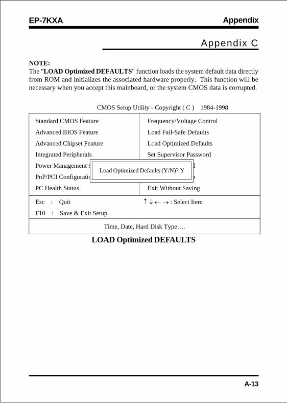
Appendix C
NOTE:The "LOAD Optimized DEFAULTS " function loads the system default data directlyfrom ROM and initializes the associated hardware properly. This function will benecessary when you accept this mainboard, or the system CMOS data is corrupted.
LOAD Optimized DEFAULTS
Load Optimized Defaults (Y/N)? Y

Appendix EP-7KXA
A-14
Page Left Blank

AppendixEP-7KXA
A-15
Appendix D
D-1 GHOST 5.1 Quick User’s Guide
Installation is very easy. You only need to copy the Ghost5 folder orGhost.exe to your hard disk.The current market version is for single Client, so the LPT and NetBiosportions will not be explained further.
Description of MenusGhost clones and backs up Disk and Partition.
In which Disk indicates hard disk optionsPartition indicates partition optionsCheck indicates check options
Disk

Appendix EP-7KXA
A-16
Disk To Disk (Disk Cloning)1. Select the location of the Source drive.2. Select the location of the Destination drive.
3. When cloning a disk or restoring the backup, set the required partitionsize as shown in the following figure.
There are 3 hard disk functions:1. Disk To Disk (disk cloning)2. Disk To Image (disk backup)3. Disk From Image (restore backup)
Important!
1. To use this function, the system must have at least 2 disks. Press theTab key to move the cursor.
2. When restoring to a destination disk, all data in that disk will becompletely destroyed.

AppendixEP-7KXA
A-17
4. Click OK to display the following confirmation screen. Select Yes tostart.
Disk To Image (Disk Backup)
1. Select the location of the Source drive.
2. Select the location for storing the backup file.

Appendix EP-7KXA
A-18
Disk From Image (Restore Backup)
1. Select the Restore file.
2. Select the Destination drive of the disk to be restored.
3. Click OK to display the following confirmation screen. Select Yes tostart.
AppendixEP-7KXA
A-19
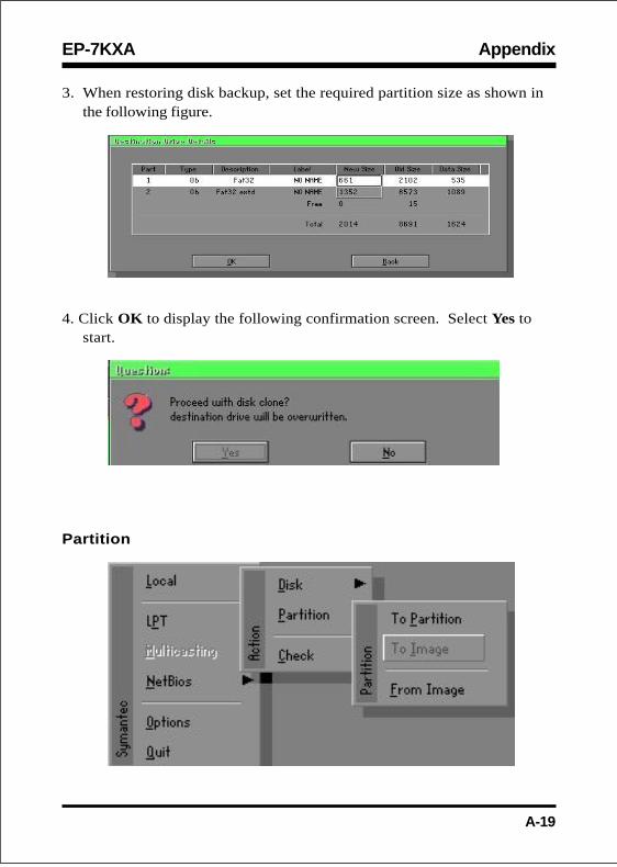
3. When restoring disk backup, set the required partition size as shown inthe following figure.
4. Click OK to display the following confirmation screen. Select Yes tostart.
Partition
Appendix EP-7KXA
A-20
2. Select the first partition to be backed up. This is usually where theoperating system and programs are stored.
There are 3 partition functions:
1. Partition To Partition (partition cloning)
2. Partition To Image (partition backup)
3. Partition From Image (restore partition)
Partition To Partition (Partition Cloning)
The basic unit for partition cloning is a partition. Refer to disk cloning forthe operation method.
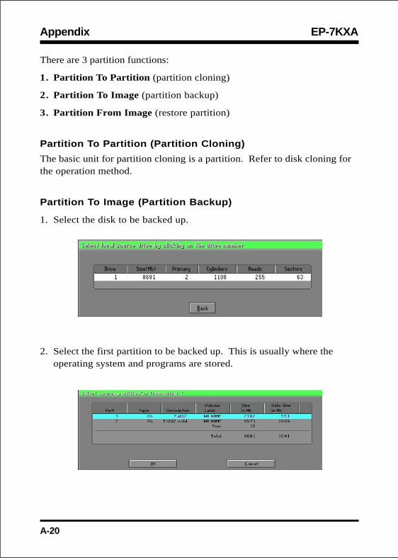
Partition To Image (Partition Backup)
1. Select the disk to be backed up.

AppendixEP-7KXA
A-21
3. Select the path and file name for storing the backup file.
4. Is the file compressed? There are 3 options:
(1) No: do not compress data during backup
(2) Fast: Small volume compression
(3) High: high ratio compression. File can be compressed to its minimum,but this requires longer execution time.
5. During confirmation, select Yes to start performing backup.
Appendix EP-7KXA
A-22
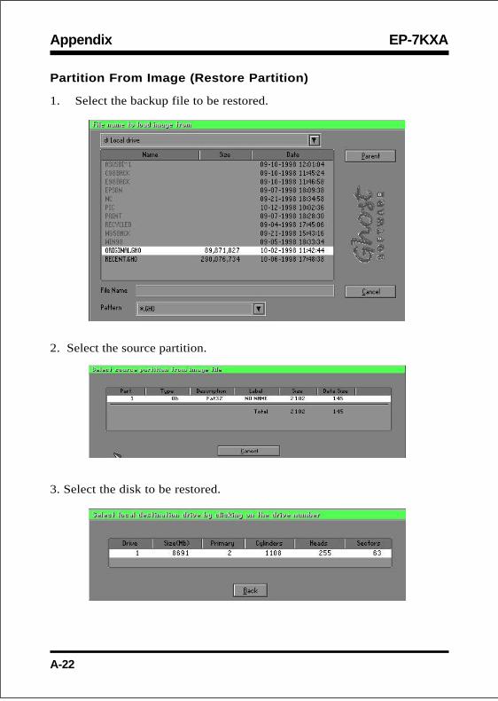
Partition From Image (Restore Partition)
1. Select the backup file to be restored.
2. Select the source partition.
3. Select the disk to be restored.

AppendixEP-7KXA
A-23
4. Select the partition to be restored.
5. Select Yes to start restoring.
Check
This function checks the hard disk or backup file for backup orrestoration error due to FAT or track error.