enhancement of bandwidth of rectangular patch antenna ... · microwave integrated circuits...
TRANSCRIPT

International Journal of Engineering Sciences & Emerging Technologies, Oct. 2012.
ISSN: 2231 – 6604 Volume 3, Issue 2, pp: 1-12 ©IJESET
1
ENHANCEMENT OF BANDWIDTH OF RECTANGULAR PATCH
ANTENNA USING TWO SQUARE SLOTS TECHNIQUES
Patil V. P.
Smt. Indira Gandhi college of Engineering, New Mumbai, INDIA [email protected]
ABSTRACT
The research in wireless communication has spurred the development of extra ordinary range of antennas, each
with its own advantage and limitations. There are many applications where space is at premium, and where
there is an urgent need for an antenna with the flexibility to efficiently combine the capabilities of multiple
antennas. In fact rapidly developing market in personal communication systems (PCS), mobile satellite
communications, direct broadband television (DBS) wireless local area networks (WLANs) suggest that demand
for Microstrip antennas and array will increase even further. Conventional Microstrip patch antennas has some
drawbacks of low efficiency, narrow bandwidth (3-6%) of the central frequency, its bandwidth is limited to a
few percent which is not enough for most of the wireless communication systems nowadays. In this paper one of
the efficient methods used for the enhancement of patch antenna bandwidth is the loading of rectangular
microstrip patch antenna with two square slots across its side surface. This type of Microstrip patch antenna
meets the requirement of operation for wireless applications. The proposed configuration is simulated and
analyzed using GENESYS software package. The VSWR, input impedance‚ and S11 performance are used for
the analysis of the different configurations. The simulated results for square slots antenna structure give
bandwidth of 311 MHZ. Feed point on the patch that gives a good match of 50 ohm. The results of the
fabricated microstrip antenna give the bandwidth of 286 MHz.
KEYWORDS
Rectangular microstrips patch antenna, Bandwidth enhancement, square, slot, Genesys.
I. INTRODUCTION
A MICROSTRIP ANTENNA (MSA) in its simplest form consists of a radiating patch on one side of
a dielectric substrate and a ground plane on the other side. The top view and side views of a
rectangular MSA (RMSA) are shown in Figure-1and 2.

International Journal of Engineering Sciences & Emerging Technologies, Oct. 2012.
ISSN: 2231 – 6604 Volume 3, Issue 2, pp: 1-12 ©IJESET
2
Figure-1: The top view of a rectangular MSA (RMSA). Figure-2: side view of patch antenna
However, other shapes, such as the square, circular, triangular, semicircular, sectoral, and annular ring
shapes are also used. Microstrip antennas are popular for their attractive features such as low profile,
low weight, low cost, ease of fabrication and integration with RF devices. The major disadvantages of
Microstrip antennas are lower gain and very narrow bandwidth [1, 2, 3]. Microstrip patch antenna
consists of a dielectric substrate, with a ground plane on the other side. Due to its advantages such as
low weight , low profile planar configuration, low fabrication costs and capability to integrate with
microwave integrated circuits technology, the microstrip patch antenna is very well suited for
applications such as wireless communications system, cellular phones, pagers, Radar systems and
satellite communications systems [4,5,6]. Several designs have been investigated and reported to
decrease the size of the antenna [7, 14] and to improve the bandwidth of the antenna [8, 9, 15].
Handset antenna has been reported with wide bandwidth [10]. Half U-slot patch antenna with shorting
wall reported in [11] with 28% impedance bandwidth.
In this paper, broadband patch antenna with two square slots across its side surface is proposed. This
type of Microstrip patch antenna meets the requirement of operation for wireless applications. The
proposed configuration is simulated and analyzed using GENESYS software package [30]. The
VSWR, input impedance‚ and S11 performance are used for the analysis of the different
configurations. The paper is divided as: section 2 presents the brief literature survey about microstrip
antenna and bandwidth enhancement techniques are explained in section 3. The structure and
dimensions of the proposed antenna is presented in section 4 followed by the result of the simulated
antenna in section 5. Finally, section 6 provides the conclusion. Results are based on an antenna
simulation software package GENESYS.
II. BRIEF LITERATURE SURVEY
The microstrip antenna concept dates back about 26 years to work in the U.S.A. by Deschamps [12]
and in France by Gutton and Baissinot [13]. Shortly thereafter, Lewin investigated radiation from
stripline discontinuities. Additional studies were undertaken in the late 1960’s by Kaloi, who studied
basic rectangular and square configurations. However, other than the original Deschamps report, work
was not reported in the literature until the early 1970’s, when a conducting strip radiator separated
from a ground plane by a dielectric substrate was described by Byron. This half wavelength wide and
several wavelength long strip was fed by coaxial connections at periodic intervals along both radiating
edges, and was used as an array for Project Camel. Shortly thereafter, a microstrip element was
patented by Munson [14] and data on basic rectangular and circular microstrip patches were published
by Howell. Weinschel developed several microstrip geometries for use with cylindrical S band arrays
on rockets. Sanford showed that the microstrip element could be used in conformal array designs for
L band communication from KC-135 aircraft to the ATS-6 satellite. Additional work on basic
microstrip patch elements was reported in 1975 by Garvin et al, Howell, Weinschel and Janes and
Wilson. The early work by Munson on the development of microstrip antennas for use as low profile

International Journal of Engineering Sciences & Emerging Technologies, Oct. 2012.
ISSN: 2231 – 6604 Volume 3, Issue 2, pp: 1-12 ©IJESET
3
flush mounted antennas on rockets and missiles showed that this was a practical concept for use in
many antenna system problems and thereby gave birth to the new antenna industry.
There are some other technique for enhancement of bandwidth of antennas is the multiple layers
which consisting of two or more metallic patches supported by one or more dielectric layers. There
are two techniques for multi-band MPA using multiple layers. Firstly the dichroic technique with
frequency band separation of 10:1 [17]. Secondly the stacking technique which uses two or three
substrates providing two or more metallic patches within the same aperture area with frequency
bandwidth of 5.6% for the stacked circular disc [18] or up to 13% with four rectangular patches [19]
or up to 33% with strip-slot-foam-inverted patch antenna [20]. Size, weight, feed fabrication, and high
coupling between stacked patches are the main disadvantages of the stacked antennas [21].Joshi and
Lohokare [22] highlighted Microstrip Patch Antenna Loaded with Magnetoinductive Waveguide.
Chen and Zhang [23] described Bandwidth enhancement of a microstrip-linefed printed wide-slot
antenna with a fractal shaped slot. A novel monopole antenna with a self-similar slot for wideband
applications [25] is designd by Song and Zhang. In[24] Kim and Junghas explained about Bandwidth
enhancement of CPW fed tapered slot antenna with multi-transformation characteristics. Kalteh [26]
has enhancd bandwidth for A Microstrip-fed UWB Circular slot antenna. In [27][28] [29] bandwidth
enhancement is presented for UWB applications.
III. TECHNIQUES OF BANDWIDTH ENHANCEMENT FOR MSA
MSA in its regular shape cannot yield multi-octave BW because of its resonant nature. Some
modification of the MSA configuration is required to obtain an octave BW. If a rectangular patch
without the substrate and ground plane is fed at the edge by a coaxial feed with a perpendicular
ground plane, then the patch will have an effective dielectric constant equal to 1 with large h. Both of
these factors yield broad BW. This modified configuration can be thought of as a planar rectangular
monopole antenna. Other configurations such as triangular, hexagonal, circular, and elliptical
monopoles also yield broad BW [12, 15]. An elliptical monopole with an ellipticity of 1.1 yields BW
of 1:11 for VSWR ≤ 2 . The most serious limitation of the MSA is its narrow BW.
3.1 Definition of BW
The BW could be defined in terms of its VSWR or input impedance variation with frequency or in
terms of radiation parameters. For the circularly polarized antenna, BW is defined in terms of the
axial ratio (AR).Therefore, before describing the various methods for increasing the BW, the various
definitions of the BW are described.
The VSWR or impedance BW of the MSA is defined as the frequency range over which it is matched
with that of the feed line within specified limits. The BW of the MSA is inversely proportional to its
quality factor Q and is given by
BW = VSWR1Q√VSWR
(1)
The BW is usually specified as frequency range over which VSWR is less than 2 (which corresponds
to a return loss of 9.5 dB or 11% reflected power). Sometimes for stringent applications, the VSWR
requirement is specified to be less than 1.5 (which corresponds to a return loss of 14 dB or 4%
reflected power). Conversion of BW from one VSWR level to another can be accomplished by
12
=112121
(2)
where BW1 and BW2 correspond to VSWR1 and VSWR2, respectively.
The expressions for approximately calculating the percentage BW of the RMSA in terms of patch
dimensions and substrate parameters is given by
%BW=
0√ (3)
Where
A=180 for
0√ ≤ 0.045, A = 200 for 0.045 ≤
0√ ≤ 0.075, A = 220 for
0√ ≥ 0.075
And W and L are the width and length of the RMSA. With an increase in W, BW increases.

International Journal of Engineering Sciences & Emerging Technologies, Oct. 2012.
ISSN: 2231 – 6604 Volume 3, Issue 2, pp: 1-12 ©IJESET
4
Another simplified relation for quick calculation of BW (in megahertz) for VSWR = 2 of the MSA
operating at frequency f in gigahertz, with h expressed in centimeters, is given by- ≅ 50ℎ2 The BW can also be defined in terms of the antenna’s radiation parameters. It is defined as the
frequency range over which radiation parameters such as the gain, half-power beam width (HPBW),
and side lobe levels are within the specified minimum and maximum limits. This definition is more
complete as it also takes care of the input impedance mismatch, which also contributes to change in
the gain.
The above definitions for BW are mainly for a linearly polarized MSA. For a circularly polarized
MSA, the BW is generally limited by its AR. This BW is the frequency range over which AR is less
than a maximum limit (e.g., 3 or 6 dB).
The main techniques used to increase the BW are presented briefly in the following sections.
3.2 Modified Shape Patches
The regular MSA configurations, such as rectangular and circular patches have been modified to
rectangular ring and circular ring, to enhance the BW. The larger BW is because of a reduction in the
quality factor Q of the patch resonator, which is due to less energy stored beneath the patch and higher
radiation. When a U-shaped slot is cut inside the rectangular patch, it gives a BW of approximately
40% for VSWR. Similar results are obtained when a U-slot is cut inside a circular or a triangular
MSA.
3.4 Planar Multi-resonator Configurations
The planar stagger–tuned coupled multiple resonators yield wide BW in the same way as in the case
of multistage tuned circuits. Several configurations are available yielding BW of 5–25%.
Various parasitic patches like narrow strips, shorted quarter-wavelength rectangular patches, and
rectangular resonator patches have been gap-coupled to the central-fed rectangular patch .These
planar multi-resonator configurations yield broad BW but have the following disadvantages:
IV. They are of large size, which makes them unsuitable as an array element.
V. There is variation in the radiation pattern over the impedance BW.
3.5 Multilayer Configurations
In the multilayer configuration, two or more patches on different layers of the dielectric substrate are
stacked on each other. Based on the coupling mechanism, these configurations are categorized as
electromagnetically coupled or aperture-coupled MSA.
Various direct-coupled multi-resonators are:
(a) RMSAs direct-coupled along radiating edges,
(b) RMSAs direct-coupled along non-radiating edges,
(c) Direct-coupled RMSAs.
3.6 Electromagnetically Coupled MSAs
In the electromagnetically coupled MSA, one or more patches at the different dielectric layers are
electromagnetically coupled to the feed line located at the bottom dielectric layer.
Alternatively, one of the patches is fed by a coaxial probe and the other patch is electromagnetically
coupled. Either the bottom or top patch is fed with a coaxial probe. The patches can be fabricated on
different substrates, and accordingly the patch dimensions are to be optimized so that the resonance
frequencies of the patches are close to each other to yield broad BW.
3.7 Stacked Multi-resonator MSAs
The planar and stacked multi-resonator techniques are combined to further increase the BW and gain.
A probe-fed single rectangular or circular patch located on the bottom layer has been used to excite
multiple rectangular or circular patches on the top layer, respectively. Besides increasing the BW,
these configurations also provide an increase in gain as well.
3.8 Effect of Feeding Techniques on bandwidth

International Journal of Engineering Sciences & Emerging Technologies, Oct. 2012.
ISSN: 2231 – 6604 Volume 3, Issue 2, pp: 1-12 ©IJESET
5
Microstrip antennas are fed by a variety of methods that are broadly classified into two main
categories-Contacting and Non-contacting.
In the contacting method, the RF power is fed directly to the radiating patch using a connecting
element such as a microstrip line. In the non-contacting method, electromagnetic field coupling is
done to transfer power between the micro strip line and the radiating patch.
The four most popular feed techniques used are:-The microstrip line, Coaxial probe (both contacting
schemes), Aperture coupling, Proximity coupling (both non-contacting schemes).
The following table indicates effect of Feeding Techniques on bandwidth which shows that proximity
coupled feed gives highest bandwidth.[16]
Table 1: Effect of Feeding Techniques on bandwidth.
Characteristics Microstrip Line Feed Coaxial Feed Aperture Coupled Feed Proximity Coupled Feed
Bandwidth 2-5% 2-5% 2-5% 13%
IV. PROPOSED DESIGN METHODOLOGY TO ENHANCE BANDWIDTH
Microstrip patch antennas are the most common form of printed antennas. They are popular for their
low profile geometry, light weight and low cost. These antennas have many advantages when
compared to conventional antennas and hence have been used in a wide variety of applications
ranging from mobile communication to satellite, aircraft and other applications.
Similarly, the different structures shapes of slots in MSA have attracted much attention in the recent
years in the microwave community for its unique properties. These structures are periodic in nature
that forbids the propagation of all electromagnetic surface waves within a particular frequency band –
called the bandgap – thus permitting additional control of the behavior of electromagnetic waves other
than conventional guiding and/or filtering structures. Various compact structures have been proposed
and studied on antenna systems. Radiation efficiency and directivity of antennas have been improved
using such structures.
4.1 Problem to be solved: Low Bandwidth of Patch Antenna In spite of the many advantages that patch antennas have in comparison to conventional antennas,
they suffer from certain disadvantages. The major drawback of such antennas is the narrow
bandwidth. In this paper, the narrow bandwidth problem of a patch antenna is tackled and solved. A
reference antenna is taken and efforts are made to improve its bandwidth by etching the feed line
connecting the patch using two square slots type patterns across side surface of rectangular microstrip
patch antenna. This is shown in fig.
4.2 Choice of Substrate
Choosing a substrate is as crucial as the design itself. The substrate itself is part of the antenna and
contributes significantly to its radiative properties. Many different factors are considered in choosing
a substrate such as dielectric constant, thickness, stiffness as well as loss tangent. The dielectric
constant should be as low as possible to encourage fringing and hence radiation. A thicker substrate
should also be chosen since it increases the impedance bandwidth. However, using a thick substrate
would incur a loss in accuracy since most microstrip antenna models use a thin substrate
approximation in the analysis. Substrates which are lossy at higher frequencies should not be used for
obvious reasons. The choice of a stiff or soft board basically depends on the application at hand. In
this paper air is selected as the dielectric material having dielectric constant as 1.
4.3 Input Impedance Matching
Impedance matching is critical in microstrip antennas since the bandwidth of the antenna depends
upon it. Besides this, a poor match results in lower efficiency also. Line fed rectangular patches may
be fed from the radiating or the non-radiating edge.
To find an impedance match along the non-radiating edge we may use the Transmission Line Model.
The input impedance along the non-radiating edge is lowest at the centre since two equally high
impedances at the two ends are transformed into a low value at the centre and connected in parallel.
Matching along the edge is also symmetrical about the mid-point of the length.
International Journal of Engineering Sciences & Emerging Technologies, Oct. 2012.
ISSN: 2231 – 6604 Volume 3, Issue 2, pp: 1-12 ©IJESET
6
4.3 Use of simulation software
In this work Genesys simulation software [30] is used for design, analysis and testing the results.
Some of the Key Features of Genesys are:
Genesys Core environment is a full-featured design environment with schematic, linear simulation,
optimization, statistical, layout, and data display capabilities. Additional capabilities can then be
extended to include RF system architecture, circuit synthesis, nonlinear circuit and 3D planer
electromagnetic simulation.
Genesys Synthesis creates high-performance circuits, accelerates routine design tasks from hours to
minutes, and enables fast make-or-buy decisions on common components. Synthesis modules for
filters, matching networks, oscillators, mixers, transmission lines, equalizers, PLL and signal control
can be added to the Genesys Core or other Genesys bundles.
Genesys Simulation offers additional RF/Microwave analysis capabilities for system architecture &
frequency planning, nonlinear circuits in the time- and frequency-domain, and planar 3D
electromagnetic (EM) characteristics. The powerful data display and processing includes MATLAB-
compatible equations and engineering math language.
V. DESIGN AND ANALYSIS
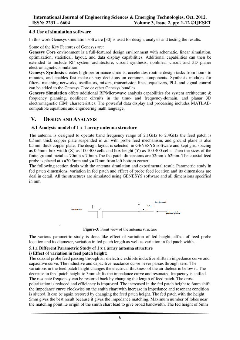
5.1 Analysis model of 1 x 1 array antenna structure
The antenna is designed to operate band frequency range of 2.1GHz to 2.4GHz the feed patch is
0.5mm thick copper plate suspended in air with probe feed mechanism, and ground plane is also
0.5mm thick copper plate. The design layout is selected in GENESYS software and kept grid spacing
as 0.5mm, box width (X) as 100-400 cells and box height (Y) as 100-400 cells. Then the sizes of the
finite ground metal as 70mm x 70mm.The fed patch dimensions are 52mm x 62mm. The coaxial feed
probe is placed at x=20.5mm and y=17mm from left bottom corner.
The following section deals with the antenna simulation and experimental result. Parametric study in
fed patch dimensions, variation in fed patch and effect of probe feed location and its dimensions are
deal in detail. All the structures are simulated using GENESYS software and all dimensions specified
in mm.
. Figure-3: Front view of the antenna structure
The various parametric study is done like effect of variation of fed height, effect of feed probe
location and its diameter, variation in fed patch length as well as variation in fed patch width.
5.1.1 Different Parametric Study of 1 x 1 array antenna structure
i) Effect of variation in feed patch height: The coaxial probe feed passing through air dielectric exhibits inductive shifts in impedance curve and
capacitive curve. The inductive and capacitive reactance curve never passes through zero. The
variations in the feed patch height changes the electrical thickness of the air dielectric below it. The
decrease in feed patch height to 3mm shifts the impedance curve and resonated frequency is shifted.
The resonate frequency can be restored back by changing the length of feed patch. The cross
polarization is reduced and efficiency is improved. The increased in the fed patch height to 6mm shift
the impedance curve clockwise on the smith chart with increase in impedance and resonant condition
is altered. It can be again restored by changing the feed patch height. The fed patch with the height
5mm gives the best result because it gives the impedance matching. Maximum number of lobes near
the matching point i.e origin of the smith chart lead to give broad bandwidth. The fed height of 5mm

International Journal of Engineering Sciences & Emerging Technologies, Oct. 2012.
ISSN: 2231 – 6604 Volume 3, Issue 2, pp: 1-12 ©IJESET
7
gives maximum lobs near matching point.
Figure-4: Impedance Variations v/s different feed patch height. Figure-5: variation in feed probe
ii) Effect of feed probe location: The coaxial probe feed it effect the antenna characteristics it can be seen that by changing the position
of the feed probe we can achieve the impedance matching for the antenna. Variation of the probe
location along the X and Y axis varies the lobes of the on the smith chart which is shown below.
Here it has been observed that the feed position of probe at X as 22mm and Y as 15.5mm is not gives
perfect impedance matching. The position of feed position of probe at X as 20.5mm and Y as 17mm
we get perfect impedance matching as it passes through the origin of the smith chart i.e matching
point.
iii) Effect of variation in feed patch length: For a patch antenna, the length is determining factor in deciding resonant condition in fundamental
operating mode. The rectangular patch resonates in its fundamental TM10 mode, where there is no
variation along the width and field is constant while there is half wavelength variation along the
length. The sinusoidal variation cancels in broadside direction and the radiation is only accomplished
by the field along the width. The resonant frequency is detuned when the length of the feed patch is
varied. When the feed patch length is 60mm, the bandwidth we get is 18MHz is observed.
When we increase the length of the feed patch to 62mm we got the bandwidth as 114MHz for return
loss -9.54dB. These differences of bandwidth are shown below graph.
iv) Effect of variation feed patch width:
For rectangular fed patch to resonate at 2.4 GHz, air dielectric. The theoretical calculated width is
62mm. It is seen that for the width of the 50 mm, the return loss is less than the width of 52mm and
approximately same bandwidth is obtained. It does not affect the resonant frequency of the antenna.
The graph shows the variation of width by trial and error method it is concluded that,the theoretical
width and practical width both are different.
Figure-6 : Return loss v/s frequency for change in Figure-7: Comparison plots of return loss for
feed patch length. different widths of feed patch
5.1.2 Final simulated results of 1 x 1 reference antenna

International Journal of Engineering Sciences & Emerging Technologies, Oct. 2012.
ISSN: 2231 – 6604 Volume 3, Issue 2, pp: 1-12 ©IJESET
8
Figure-8: Return Loss Figure-9: VSWR
For reference antenna bandwidth obtained is as 109MHz.
5.2 Modified structure of Microstrip Antenna: The following are the various structural changes done in the modified MSAs
Figure-10: Feed patch Figur-11: View of final structure
5.2.1 Parametric study for the modified Microstrip Antenna: i) Effect of feed probe position: By changing the position of the feed probe location we can see the
variations in the impedance on smith chart. It also varies the return loss of the antenna which affect
the bandwidth of the antenna.
ii) Effect of notch size:
The notch or shape which cuts in the patch affects the antenna parameter. Here we cut the square at
both the radiating edge of the feed patch. The graph below shows the variation in return loss as well
as variation in the impedance of the antenna. Here we consider two type of square shape of 6mm x
6mm and 12mm x 12 mm. It is find that bandwidth is more in the structure having the notch of the
6mm x 6mm rather than the 12mm x 12mm and it also shows that the impedance matching is perfect
for the notch of 6mm x 6mm rather than 12mm x 12mm.
Figure-12: Impedance variation v/s different feed Figure-13: return loss variation v/s different feed location
patch location.

International Journal of Engineering Sciences & Emerging Technologies, Oct. 2012.
ISSN: 2231 – 6604 Volume 3, Issue 2, pp: 1-12 ©IJESET
9
Figure-14 : Return Loss v/s different notch size Figure-15 : Impedance variation V/s different
notch size
5.2.3 Simulated results of modified Microstrip Antenna:
Frequency Figure-16: Return Loss Figure-17: VSWR
Figure-18: Impedance at resonance Figure-19: Antenna Hardware
Frequency
Bandwidth obtained after simulation= 311.845Mhz In this antenna lower and upper conducting layers’ material is copper metal of thickness 0.5mm. The
size of ground metal is 70mm x 70mm and the size of feed patch is 62mm x 52mm. The coaxial feed
is used for that purpose SMA connector of diameter 2mm is used. This connector is connected at
(20.5mm,17mm) from the left bottom corner of the feed patch.
5.3 Results of fabricated Modified Patch Antenna
The proposed antenna is fabricated for the designed dimensions and its results are tested by using
spectrum analyzer. The fig shows the results for return loss, impedance. and it is seen that the results
of simulated antenna structure and fabricated structure are almost similar .

International Journal of Engineering Sciences & Emerging Technologies, Oct. 2012.
ISSN: 2231 – 6604 Volume 3, Issue 2, pp: 1-12 ©IJESET
10
Figure-20: Measurement Of Return Loss Figure-21: Impedance Measurement Impedance
Measurement is done for Return Loss ( -37.28dB at 2.205 GHz) and Impedance Measurement (50Ω at
2.205GHz).Bandwidth obtained on spectrum analyses at -9.54dB: BW= (2.383-2.102) GHz = 286MHz
5.4 Comparison of Simulated and Fabricated Results
The table 2 shows the comparative results for return loss, impedance. VSWR and bandwidth and it is
seen that the results of simulated antenna structure and fabricated structure are almost similar. The
impedance bandwidth of the designed antenna is 109 MHZ .Whereas the impedance bandwidth of the
antenna with two square slots across side surface of rectangular patch antenna is 311.84 MHZ. That
means, the bandwidth enhancement is approximately (202 MHZ) higher than that of original case
(patch without slot, Bandwidth 109 MHZ). The return loss of simulated antenna is -27 db whereas that
of fabricated antenna is -37.28 db. The impedance at resonance for both simulated and fabricated
antenna is found same i.e. 50 ohms.
Table 2: performance comparison of Simulated and Fabricated Result of micro-strip patch antenna
Type of Structure used Result Of Simulated Antenna structure By Genesys Software
Results of Fabricated Antenna structure
Fabricated Modified
Antenna
-37.28 50 286MHz
VI. CONCLUSION In this paper the rectangular patch Antenna with (50) ohm coaxial feed has been designed. A small
broadband antenna has been introduced and bandwidth is enhanced by inserting two square slots on
side surface of rectangular patch antenna The impedance bandwidth of the designed antenna is 109
MHZ .Whereas the impedance bandwidth of the antenna with two square slots across side surface of
rectangular patch antenna is 311.84 MHZ. That means, the bandwidth enhancement is approximately
(202 MHZ) higher than that of original case (patch without slot, Bandwidth 109 MHZ). The improved
antenna characteristic is satisfactory for most of the wireless system.
REFERENCES
[1] Thomas A. Milligan. 2nd Ed. Modern antenna design. pp. 318-354.
[2] A.K Bhattacharjee, S.R Bhadra, D.R. Pooddar and S.K. Chowdhury. 1989. Equivalence of impedance and
radiation properties of square and circular microstrip patches antennas. IEE Proc. 136 (Pt, H, no. 4): 338-342.
Return Loss(Db) Impedance At
Resonance
VSWR
Bandwidth
Reference Antenna
-27dB 50 1.05 109MHz
Modified Antenna -40dB 50 1.00 311.845MHz

International Journal of Engineering Sciences & Emerging Technologies, Oct. 2012.
ISSN: 2231 – 6604 Volume 3, Issue 2, pp: 1-12 ©IJESET
11
[3] R. G. Voughan. 1988. Two-port higher mode circular microstrip antennas. IEEE, Trans. Antennas Propagat.
36(3): 309-321.
[4] W.L. Stutzman and G.A. Thiele, Antenna Theory and Design, 2nd ed. New York: Wiley, 1998
[5] C.A. Balanis, Antenna Theory, 2nd ed. New York: John Wiley & Sons, Inc., 1997.
[6] H. F. AbuTarboush, H. S. Al-Raweshidy, “A Connected E-Shape and U-Shape Dual-Band Patch Antenna
for Different Wireless Applications”, the Second International EURASIP Workshop on RFID Technology, July,
2008.
[7] Nashaat DM, Elsadek H. Miniturized E-shaped dual band PIFA on FR4 substrates. Radio Science
Conference, 2006 NRSC 2006 Proceedings of the Twenty Third National. 2006;0:1-6.
[8] Fujimoto T. Wideband stacked square microstrip antenna with shorting plates. IEICE Trans B:
Communications. 2008 May 1;E91-B(5):1669-72. Authorized licensed use limited to: Brunel University.
Downloaded on November 29, 2009 at 15:04 from IEEE Xplore. Restrictions apply.
[9] Lin S-, Row J-. Bandwidth enhancement for dual-frequency microstrip antenna with conical radiation.
Electronics Letters. 2008;44(1):2-3.
[10] Anguera J, Cabedo A, Picher C, Sanz I, Ribo M, Puente C. Multiband handset antennas by means of
groundplane modification. Antennas and Propagation International Symposium, 2007 IEEE. 2007:1253-6.
[11] Mak CL, Chair R, Lee KF, Luk KM, Kishk AA. Half U-slot patch antenna with shorting wall. Electronics
Letters. 2003;39(25):1779-80.
[12] G. A.Deschamps, “Microstrip microwave antennas”, presented at the 3rd
USAF Symp. On antennas, 1953.
[13] H. Gutton and G. Baissinot, “Flat aerial for ultra high frequencies”, French patent No. 703113, 1955.
[14] R. E. Munson, “Single slot cavity antennas assembly”, U.S. patent No. 3713 162, January 23, 1973.
[15] Reference data for radio engineers, 5th
ed. Indianapolis, IN: Howard W. Sams, Oct. 1968, Ch-22, pp 25-27.
[16] K.P. Ray and G. Kumar, “Broadband Microstrip Antennas”, Archtech House, ISBN: 1-58053-244-6, 2003.
[17]. James, J. R. and G. Andrasic, “Super dichroic microstrip antenna arrays,” Proc. IEEE, 135 H, 304–312,
1988.
[18] Long, S. A. and M. D. Walton, “A dual frequency stacked circular disc antenna,” IEEE Trans. Ant. Prop.,
Vol. AP-27, No. 2, 270– 273, 1979.
[19]. Legay, H. and L. Shafai, “New stacked microstrip antenna with large bandwidth and high gain,” IEE Proc.
Micro. Ant. Prop., Vol. 141, No. 3, 99–204, 1994.
[20]16. Zurcher, J. F. and F. E. Gardiol, Broad-band Patch Antennas, Artech House, Inc., London, 1995.
[21]. Long, S. A. and M. D. Walton, “Mutual coupling between stacked square microstrip antennas fed on their
diagonal,” IEEE Trans. Ant. Prop., Vol. 39, No. 7, 1049–1051, 1991.
[22] J. G. Joshi, S. S. Pattnaik, S. Devi and M. R. Lohokare, “Microstrip Patch Antenna Loaded with
Magnetoinductive Waveguide,” Proceedings of 12th National Symposium on Antennas and Propagation,
Cochin, 6-10 December 2010, pp. 101-105.
[23] Chen, W. L., G. M. Wang, and C. X. Zhang, “Bandwidth enhancement of a microstrip-linefed printed wide-
slot antenna with a fractalshaped slot” IEEE Transactions on Antennas Propagation, Vol. 57, No. 7, 21762179,
2009.
[24] Song, K., Y.-Z. Yin, and L. Zhang, “A novel monopole antenna with a self-similar slot for wideband
applications” Microwave and Optical Technology Letters, Vol. 52, No. 1, 9597, 2010.
[25] Kim, H. and C.-W. Jung, “Bandwidth enhancement of CPW fed tapered slot antenna with multi-
transformation characteristics” Electronics Letters, Vol. 46, No. 15,
10501051, 2010.
[26] A.A.Kalteh, R.Fallahi, and M.G.Roozbahani, “A novel Microstrip-fed UWB Circular slot antenna with 5-
Ghz Band-notch characteristics” IEEE International Conference on Ultral-wideband (ICUWB2008), vol.1,
2008, pp.117-120.

International Journal of Engineering Sciences & Emerging Technologies, Oct. 2012.
ISSN: 2231 – 6604 Volume 3, Issue 2, pp: 1-12 ©IJESET
12
[27] M.Ojaroudi, G.Ghanbari, N.Ojaroudi, C.Ghobadi, “Small square monopole antenna for UWB applications
with Variable frequency band-notch function”, IEEE Antennas and Wireless Propagation Letters, vol.8, 2009.
[28] H.w.Liu, C.H.Ku, T.S.Wang, C.F.Yang, “Compact monopole antenna with bandnotched characteristic for
UWB applications”, IEEE Antennas and Wireless Propagation Letters, vol. 9, 2010.
[29] B.Ahamadi, R.F.Dana, “A miniaturized monopole antenna for ultra-wideband applications with band-
notch filter”, IET Microwave antennas Propagations, vol.3, 2009, pp.1224-123.
[30] An antenna simulation software package GENESYS by Agilent and its tutorial available at
www.home.agilent.com
AUTHOR PATIL V.P. is currently working as a faculty member in Electronics and
Telecommunication Engineering department in Smt. Indira Gandhi college of Engineering.
New Mumbai. He is graduate in B.E. and post graduate in M.TECH (ELECTRONICS
DESIGN AND TECHNOLOGY).He is having 25 years of experience in teaching and
administrations in Engineering colleges. His area of research is in computer
communication networking and microwave engineering.