enhanced thermoelectric performance of half heusler and ... nisn half heusler alloys, 0.25%, 0.5%...
TRANSCRIPT

I
Enhanced thermoelectric performance of Half Heusler and Silicon Germanium via
nanostructuring
Di Wu
B.S., University of Science and Technology of China, P.R.China
A Dissertation presented to the Graduate Faculty
of the University of Virginia in Candidacy for the Degree of
Doctor of Philosophy
Department of Physics
University of Virginia
August 2013
______________________________
______________________________
______________________________
______________________________
II
Abstract
Nanostructured Half Heusler alloys MNiSn, MCoSb (M=Hf, Zr and Ti) and SiGe
nanocomposites were synthesized with high energy vibrational ball mill, followed by spark
plasma sintering (SPS) consolidation. The thermoelectric properties were measured from room
temperature to 1100K, the dependence of thermoelectric properties on consolidation parameters
and microstructures were investigated. A differential effective medium (DEM) model was also
developed to evaluate the lattice thermal conductivity in heterogeneous two-phase systems.
In the case of N-type Hf0.75Zr0.25NiSn Half Heusler alloys, 0.25%, 0.5% and 1% V were
doped into Hf site; up to 40% thermopower enhancements were observed from 300K to 600K,
meanwhile, no obviously change of electrical conductivities were detected, indicating that the
enhancement of thermopower came from localized density of states (DOS) enhancement at the
Fermi level. The enhancement of thermopower enhancement was discussed within Mott
expression and this conclusion was further supported by low temperature specific heat
measurements, which clearly showed the DOS at the Fermi level was increased by 88% after 1%
V was doped into Hf site. Nanostructuring technique was also performed to achieve better ZT
performance. N-type Hf0.6Zr0.4NiSn0.995Sb0.005 nanocomposites were synthesized via mechanical
alloys and SPS consolidation, thermopower got enhanced and lattice thermal conductivity was
suppressed, compared with the corresponding bulk form; furthermore, 10% Hf atoms being
replaced by Ti atoms was proved to further reduce the lattice thermal conductivity, eventually

III
leading to a dimensionless figure of merit ZT as high as 1.0 at 823K. Second-phase ZrO2
nanoparticles being introduced into P-type Hf0.3Zr0.7CoSn0.3Sb0.7 matrix was also proved to
effectively increase photon scattering intensity and result in an enhanced figure of merit ZT=0.85
at 1050K.
In the case of SiGe nanocomposites, the dependence of thermoelectric properties on SPS
consolidation parameters was investigated, it was concluded that sufficient sintering temperature
and holding time were necessary to obtain nonporous nanocomposites. It was also found that
severe grain growth took place during SPS consolidation, probably due to the relatively small
mismatching potentials at the boundaries of coherent nanocrystals. Second-phase nanoinclusions
and core-shell structures were proved to effectively impede the grain growth; moreover, the
incoherent interfaces introduced by nanoinclusions also increased phonon scattering intensity
and brought energy filtering effect, resulting in reduction in lattice thermal conductivity and
enhancement in thermopower. ZT~1.2 at 1123K was achieved in nanostructured N-type
Si80Ge20P2 , while ZT~0.75 at 1123K was achieved in P-type counterpart Si80Ge20P2.
At the end, to evaluate the lattice thermal conductivity in a heterogeneous two-phase system,
the differential effective medium (DEM) model was developed based on conventional average T-
matrix approximation (ATA). The advantage of DEM over ATA is that DEM not only expands
the applicability of effective medium approach from small volume factions to the whole range of
volume fraction from 0 to 1, but also inherently includes the multiple scattering which dominates
at high volume factions but wasn’t well considered in ATA with single particle scattering
approximation. A revised effective scattering cross section, together with the grain size
dispersion, demonstrated a further reduction in lattice thermal conductivity.
IV
Table of contents
Abstract………………………………………………………………………………………II
Table of contents……………………………………………………………………………..IV
List of figures………………………………………………………………………………VIII
List of tables………………………………………………………………………………..XIII
1. Background of thermoelectricity…………………………………………………………..1
1-1. Discovery of thermoelectric effects…………………………………………………..1
1-2. Figure of merit ZT and efficiency of thermoelectrics………………………………..8
1-3. Semiconductors as optimal thermoelectric materials…………………………........14
1-4. State-of-the-art TE materials………………………………………………………..17
1-5. Motivation…………………………………………………………………………..22
2. Sample synthesis and characterization……………………………………………………25
2-1. Sample synthesis……………………………………………………………………25
2-1-1. Arc melting……………………………………………………………………..25
2-1-2. Annealing…………………………………………………………………... .....26
2-1-3. Introduction melting……………………………………………………………27
2-1-4. Solid state reaction……………………………………………………………..27

V
2-1-5. Melting spinning……………………………………………………………….29
2-1-6. Ball milling……………………………………………………………………..30
2-1-7. Spark plasma sintering…………………………………………………………31
2-1-8. Sample preparation for SEM…………………………………………………..33
2-1-9. Sample preparation for TEM…………………………………………………..34
2-2. Sample characterization…………………………………………………………….35
2-2-1. X-Ray Diffraction……………………………………………………………..35
2-2-2. Atomic Force Microscopy…………………………………………………….36
2-2-3. “homemade” high temperature probe……………………………………..….37
2-2-4. ZEM-3…………………………………………………………………………40
2-2-5. Thermal conductivity………………………………………………………….41
2-2-6. Hall effect……………………………………………………………………...43
3. Thermoelectric properties improvement on Half Heusler alloys via nanostructuring …...45
3-1. Introduction of Half Heusler (HH)…………………………………………………46
3-2. Resonant states……………………………………………………………………..48
3-2-1. Background…………………………………………………………………...48
3-2-2. Experiments…………………………………………………………………..50
3-2-3. Discussion…………………………………………………………………….52
3-2-4. Conclusions of resonant states……………………………………………….58
3-3. Nanostructuring……………………………………………………………………59
3-3-1. Exploring for proper ball mill vessel…………………………………………60
3-4. Efforts on thermopower enhancement via energy filtering…………………..….62
3-4-1. Monolithic N-type HH nanocomposite……………………………………....66
3-4-2. Nanoparticles embedded P-type bulk HH…………………………………....71
3-5. Reduction on thermal conductivity………………………………………………..77

VI
3-5-1. Monolithic nanocomposite…………………………………………………...78
3-5-2. Nanoparticles embedded in bulk……………………………………………..79
3-6. Mass fluctuation effect on lattice thermal conductivity…………………………..81
3-7. Conclusions………………………………………………………………………..84
4. Nanostructured Silicon Germanide as prospective thermoelectrics……………………....86
4-1. Sample synthesis…………………………………………………………………..87
4-2. Grain size vs. BM time…………………………………………………………….88
4-3. Porosity vs. sintering temperature…………………………………………………89
4-4. Grain growth in SPS consolidation process……………………………………….91
4-5. Heterogeneous nanophase…………………………………………………………97
4-6. Core-shell structure……………………………………………………………….102
4-7. Conclusions and future work………………………………………………….111
5. Effective Medium Theory (EMT)………………………………………………………..113
5-1. Average T-matrix Approximation (ATA) and Coherent Potential Approximation (CPA)
……………………………………………………………….114
5-1-1 ATA…………………………………………………………………………..114
5-1-2 CPA…………………………………………………………………………..116
5-2. Differential Effective Medium (DEM) approach………………………………...117
5-3. Comparison of DEM and ATA…………………………………………………..120
5-4. DEM with inherently implemented multiple scattering………………………….127
5-5. Effective scattering cross-section………………………………………………...135
5-5-1. Scattering cross-section……………………………………………………...136
5-5-2. Grain size dispersion………………………………………………………...138
5-5-3. Validation of effective scattering cross section treatment in DEM………….141
5-5-4. Comparison with PbS-PbSe nanocomposite…………………………………143

VII
5-5-5. Prediction on ZrNi2Sn/ZrNiSn Full Heusler-Half Heusler nanocomposite.....146
5-5-6. Conclusions…………………………………………………….……………..148
5-6. Summary and future work of DEM approach………………………………………149
6. Conclusions………………………………………………….…………………………….151
7. Acknowledgements…………………………………………….………………………….154
Reference……………………………………………………………….…………………….155
VIII
List of figures
Figure 1-1 The Seebeck effect………………………………………………………………….2
Figure 1-2 The Peltier effect……………………………………………………………………3
Figure 1-3 The Thomson effect………………………………………………………………...6
Figure 1-4 A typical thermoelectric module…………………………………………………....8
Figure 1-5 The dependence of normalized efficiency of TE engine on figure of merit ZT…13
Figure 1-6 The dependence of TE properties on carrier concentrations……………………….15
Figure 1-7 State-of-the-art N-type bulk TE materials …………………………………………18
Figure 1-8 State-of-the-art P-type bulk TE materials ………………………………………….18
Figure 1-9 A typical energy path in gasoline fueled internal combustion engine vehicle……...23
Figure 2-1 A schematic “homemade” high temperature thermoelectric probe ………….37
Figure 2-2 ZEM-3 system made by ULVAC-RIKO Inc……………………………………….40
Figure 3-1 Crystal structure of MNiSn (M=Hf, Zr, Ti) Half Heusler………………………….46
Figure 3-2 Localized resonant states over a narrow energy range ER at Fermi level………….49
Figure 3-3 (a) Powder XRD scan (b) SEM image of surface micrograph and (c) EDS line scan of
(Hf0.75Zr0.25)0.99V0.01NiSn along the yellow arrow in (b)……………………………………….51
Figure 3-4 Thermopower in the range of (a) 300K to 1100K (b) 300K to 700K, and (c) electrical
resistivity (d) power factor for V doped HH (Hf0.75Zr0.25)1-xVxNiSn, with x=0% (open square),
0.24% (gray circle), 0.63% (gray triangle) and 0.78% (black pentagon)………….….52
Figure 3-5 Plots of 2kBIn(ρ) vs. 1/T, with slopes representing width of band gaps. From top to
bottom, the plots are: 0.63% (dark grey triangle), 0.24% (light grey circle), 0.78% (black
pentagon) and 0% (open square) V- doped Hf0.75Zr0.25NiSn separately………………………53

IX
Figure 3-6 The dependence of carrier concentration n, carrier mobility μ, Seebeck coefficient S
and carrier effective mass m* on V doping level in intrinsic Hf0.75Zr0.25NiSn alloys.…….......56
Figure 3-7 The dependence of heat capacity Cp on temperature at temperatures ranging from
1.8K to 5.0K in V doped Hf0.75Zr0.25NiSn alloys, the inset shows that dependence of the Seebeck
coefficient at room temperature and density of state at the Fermi level on V doping level.
…………………………………………………………………………………………………58
Figure 3-8 X-Ray Diffraction patterns of as-cast Half Heusler Hf0.6Zr0.4NiSn0.995Sb0.005 (black)
and corresponding powders that were ball milled in normal iron vial set (blue) and that in ZrO2
vial set (red) respectively.……………………………………………………………………..62
Figure 3-9 The preferential scattering mechanism of charge carriers in conduction band through
grain boundary of barrier height εb …………………………………………………………….65
Figure 3-10 X-Ray Diffraction patterns of (a) N-type Hf0.6Zr0.4NiSn1-xSbx (x=0.005, 0.02) and (b)
P-type Hf0.3Zr0.7CoSn0.3Sb0.7 with ZrO2 impurities……………………………………………67
Figure 3-11 (a)(b) SEM scanning, (c)(d) TEM scanning and (e) Selected Area Diffraction pattern
on 15hrs Ball Milled N-type Hf0.6Zr0.4NiSn0.995Sb0.005 alloy…………………………………..68
Figure 3-12 Measured electrical resistivity (Ohm*m) and thermopower S (V/K) of N-type Half
Heusler Hf0.6Zr0.4NiSn0.995Sb0.005 which was SPS at 1000 after 15 hours’ BM (red square), the
comparison with its analogue composite without BM was presented in black square…….70
Figure 3-13 Power factor S2T/ρ dependent on temperature in monolithic nanostructured
Hf0.6Zr0.4NiSn0.995Sb0.005………………………………………………………………………70
Figure 3-14 (a) Microstructure of P-type HH Hf0.3Zr0.7CoSn0.3Sb0.7 under TEM, and selected area
diffraction as well as EDS at (b) grain area B (c) matrix area E……………………………….73
Figure 3-15 (a)(b) SEM scanning of fractured P-type Hf0.3Zr0.7CoSn0.3Sb0.7, and (c) Energy
Dispersive Spectroscopy line scan across the path shown in (b)……………………………....74
Figure 3-16 (a) Thermopower S (μV/K) and (b) Electrical resistivity ρ (μΩ*cm) of P-type
Hf0.3Zr0.7CoSn0.3Sb0.7 with 0% (black square), 1% (blue triangle) and 2% (red star) ZrO2
nanoparticles……………………………………………………………………………………75
Figure 3-17 Seebeck coefficient and electrical resistivity of nominal 1%, 2% and 4% ZrO2
dispersed P-type HH Hf0.3Zr0.7CoSn0.3Sb0.7……………………………………………………..76
Figure 3-18 (a)Total thermal conductivity (solid lines) and lattice thermal conductivity (solid
squares) (b) figure of merit ZT of N-type HH Hf0.6Zr0.4NiSn0.995Sb0.005 with 0hr (black), 10hrs
(blue) and 15hrs (red) Ball Milling time .………………...……………………………………...79

X
Figure 3-19 Lattice thermal conductivity of P-type HH Hf0.3Zr0.7CoSn0.3Sb0.7 bulk (grey) and
corresponding nanocomposistes with 1% (blue), 2% (black) and 4% (red) ZrO2 nanoparticles.80
Figure 3-20 The dependence of figure of merit ZT on temperature in 1%, 2% and 4% ZrO2
dispersed Hf0.3Zr0.7CoSn0.3Sb0.7………………………………………………………………..81
Figure 3-21 Lattice thermal conductivity of Hf0.6Zr0.4NiSn0.995Sb0.005 with 0%, 10%, and 20% Hf
atoms replaced by smaller Ti atoms……………………………………………………………83
Figure 3-22 Figure of merit ZT achieved of Half Heusler alloys (a) N-type: ZT=1.0 at 850K in
monolithic Ti0.1Hf0.5Zr0.4NiSn0.995Sb0.005 (b) P-type: ZT=0.85 at 1050K in 2% ZrO2 nanoparticles
dispersed Hf0.3Zr0.7CoSn0.3Sb0.7.. ……………………………………………………………...85
Figure 4-1 TEM images of nanoscaled aggregates under different magnifications for Si80Ge20P2
ball milled 5 hours……………………………………………………………………………….89
Figure 4-2 TEM images of nanoscale aggregates under different magnifications for Si80Ge20P2
ball milled 15 hours……………………………………………………………………………...89
Figure 4-3 Electrical resistivity (a), Seebeck coefficient (b) and Power Factor (c) of Si80Ge20P2
sintered at 900 , 1000 and 1100 separately……………………………………………...91
Figure 4-4 XRD pattern of SGP-T1-05 and SGP-T1-15, the inset shows corresponding peaks at
(111)……………………………………………………………………………………………..92
Figure 4-5 Lattice thermal conductivity of SGP-T1-05 and SGP-T1-15………………………..93
Figure 4-6 XRD pattern of Si80Ge20P2 nanopowders (black) after 15 hours BM and its solidified
bulk (blue) analogue, the inset provides enlarge comparison of diffraction peaks at (111)…….94
Figure 4-7 Grains of SPS consolidated Si80Ge20P2 with 5 hours BM time under JOEL 2000FX
showing the huge majority grains in (a)(b), and HRTEM Titan showing the existence of small
minority grains in (c)(d)………………………………………………………………………….95
Figure 4-8 Comparison of lattice thermal conductivity and ZT between our samples with
significant grain growth (black squares) and Boston College without grain growth (black curve)
……………………………………………………………………………………….…………96
Figure 4-9 Si80Ge20P2 nanocomposites with 15 hours ball mill time examined under JEOL
2000FX…………………………………………………………………………………………..97
Figure 4-10 TEM image of Yttria Stabilized Zirconia (YSZ) nanopowders………………..98
XI
Figure 4-11 TEM images of SPS condensed Si80Ge20P2 nanocomposites (BM for 5hours) with 0%
YSZ (a)(b), 5% YSZ (c)(d) and 10%YSZ (e)(f) nanoparticles…….………………………...99
Figure 4-12 EDS scanning over light smaller and dense light grains for 5% YSZ dispersed
Si80Ge20P2, indicating the fact that light grains are YSZ, dense grains Si80Ge20P2…………….101
Figure 4-13 Thermal conductivity, power factor and figure of merit of 0%, 2%, 5% and 10%
YSZ nanoparticles dispersed Si80Ge20P2………………………………………………..102
Figure 4-14 A enlarged band gap Eg of a quantum dot due to size effect, compared with its bulk
counterpart and single molecule with LUMO-HOMO gap…………………………………….104
Figure 4-15 Core-shell structures of 3 different types classified by the relative position of
conduction and valence band of the core and the shell, with blue and red blocks represent core
and shell band structures individually………………………………………………..……..…105
Figure 4-16 (a)The Type I CdSe/CdS core/shell structure and (b) the Type II CdSe/CdTe core-
shell structure…………………………………………………………………………………...106
Figure 4-17 The pseudo core (red circle)/shell (green circle) structure of Si80Ge20B1.7/YSZ
nanocomposite…………………………………………………………………………… .107
Figure 4-18 Comparison of thermoelectric properties for Si80Ge20B1.7/SiO2(blue square) and
Si80Ge20B1.7/TiO2 (red square) core-shell structures with sole Si80Ge20B1.7 nanocomposite (black
square)………………………………………………………………………………………108
Figure 4-19 Conduction and valence band edges alignment of SiGe core and SiO2/TiO2/YSZ
shell……………. ………………………………………………………………………………109
Figure 4-20 Figure of merit ZT in Si80Ge20B1.7/SiO2 and Si80Ge20B1.7/TiO2………………...…110
Figure 5-1 Configuration of adding dϕ of second phase in DEM regime…………………….118
Figure 5-2 Dependence of lattice thermal conductivity κph in YSZ/CoSb3 nanoparticle/matrix
system on volume fraction ϕ at 300K, with DEM (solid lines) and ATA (dash lines) calculations;
the grain size of YSZ nanoparticles are set to be 50, 20, 20, 5 nm separately.……………….123
Figure 5-3 Dependence of lattice thermal conductivity κph in CoSb3/CoSb3 nanoparticle/matrix
system on volume fraction ϕ at 300K, with DEM (solid lines) and ATA (dash lines) calculations;
the grain size of YSZ nanoparticles are set to be 50, 20, 20, 5 nm separately.……………….124

XII
Figure 5-4 Lattice thermal conductivity dependence on interface density Φ, in YSZ/CoSb3
naoncomposite, for grain size is equal to 50,20,10 and 5 nm separately…………………126
Figure 5-5 Independent-particle scattering in low volume fractions vs. multiple scattering in high
volume fractions……………………………………………………………………………….127
Figure 5-6 Comparison between multiple scattering and independent-particle scattering
3ϕ/2.……………………………………………………………………………………… .129
Figure 5-7 DEM Calculated lattice thermal conductivity k*(ϕ)DEM with F(ϕ) in Eqn (5-16)-
multiple scattering and F(ϕ)=3ϕ/2-independent particle scattering in core-shell structure of
Si/ZrO2 at grain size d=50, 20, 10 and 5 nm.……………………………………………..132
Figure 5-8 DEM Calculated lattice thermal conductivity k*(ϕ)DEM with F(ϕ) in Eqn (5-16)-
multiple scattering and F(ϕ)=3ϕ/2-independent particle scattering in core-shell structure of
Si80Ge20/YSZ at grain size d=50, 20, 10 and 5 nm.……………………………………….133
Figure 5-9 Lattice thermal conductivity κph of Si/Ge nanocomposite dependence on Si
nanoparticles’ volume fraction ϕ at 300K, with an average grain size of d0=10nm. DEM
simulations with different grain size dispersions (blue-fixed grain size d=d0, green-standard
deviation of 0.289d0 and red-standard deviation of 0.577d0) are compared with Nan’s EMA
(triangles), Minnich’s EMA (black solid line) and Jeng’s MC simulation (asterisks)………143
Figure 5-10 Lattice thermal conductivity κph of PbS/PbSe nanocomposite dependence on PbS
nanoparticles’ volume fraction ϕ at 300K, the comparisons are performed among experimental
data (black asterisks), KD theory for solid solutions (black line) and DEM simulations with grain
size distribution function F5(x) (red line)………………………………………………….145
Figure 5-11 Figure 5-11 Dependence of lattice thermal conductivity κph of ZrNi2Sn/ZrNiSn
nanocomposite on ZrNi2Sn nano phase’s volume fraction ϕ at 300K. Two series of plots are
presented corresponding to average grain size d0=5 nm and 10 nm individually, DEM
simulations for different grain size dispersions are distinguished by colors (blue-fixed grain size,
green-standard deviation of 0.289d0 and red-standard deviation of 0.577d0).…………….147

XIII
List of tables
Table 1-1 Thermoelectric properties of nanostructured materials at optimal operation
temperatures, values in the parentheses correspond to their normal bulk types……………….19
Table 3-1 Thermoelectric properties of V-doped Hf0.75Zr0.25NiSn…………………………….55
Table 5-1 The parameters used in nanocomposite calculations for DEM and ATA………......122
Table 5-2 Parameter used in the core-shell systems of Si/ZrO2 and Si80Ge20/YSZ, at T =
1100K. ……………………………………………………………………………………...131
Table 5-3 Spherical nanoparticles size dispersion functions dependence effective scattering cross
section for ErAs/In0.53Ga0.47As nanocomposite with d0=10nm. ………………………………139
Table 5-4 - Parameters of different composites used in this work, at room temperature T=300K
………………………………………………………………………………………………....142
1
1. Background of thermoelectricity
Thermoelectricity is a bidirectional process that can be understood as follows: the temperature
difference across a piece of material produces a potential difference or, vice versa, an electrical potential
difference applied on the material produces a temperature difference. The materials capable of
conducting heat-electricity energy conversion are thus named thermoelectric materials or
thermoelectrics. Thermoelectric materials can be utilized to build thermoelectric generators or
thermoelectric coolers, depending on whether the process is heat-electricity conversion or the reverse.
1-1 Discovery of thermoelectric effects
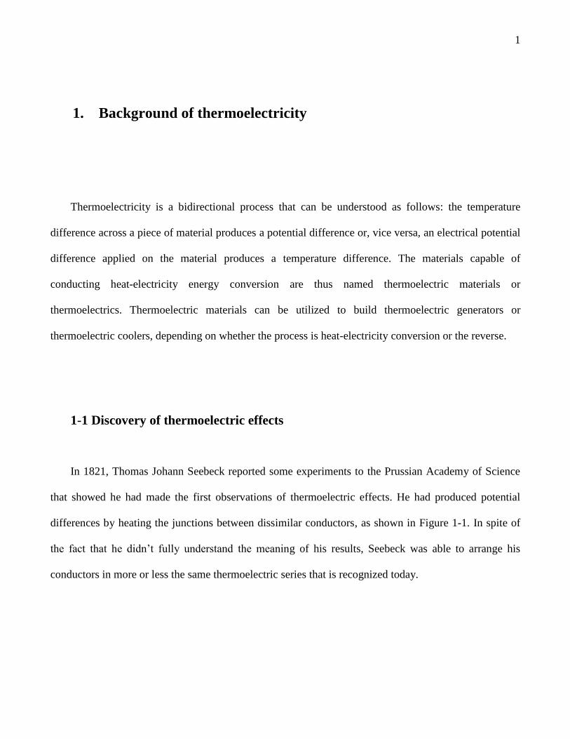
In 1821, Thomas Johann Seebeck reported some experiments to the Prussian Academy of Science
that showed he had made the first observations of thermoelectric effects. He had produced potential
differences by heating the junctions between dissimilar conductors, as shown in Figure 1-1. In spite of
the fact that he didn’t fully understand the meaning of his results, Seebeck was able to arrange his
conductors in more or less the same thermoelectric series that is recognized today.

2
Figure 1-1 The Seebeck effect.
Thirteen years later, in 1834, Jean Charles Athanase Peltier, a French watchmaker, published some
results that showed that he had discovered a second thermoelectric effect. Specifically, when a current
was passed through a junction between two different conductors, heat was absorbed or generated
depending on the direction of the current, as shown as Figure 1-2. This effect is superimposed upon, but
quite distinct from, the Joule resistance, heating effect of which usually associates with the passage of an
electric current. Like Seebeck, Peltier did not understand the true significance of his result.
Independently, in 1838, Lenz demonstrated that water could be frozen at a Bi-Sb junction by the passage
of a current; when the current was reversed, the ice could be melted.

3
Figure 1-2 The Peltier effect.
As we now know, the Seebeck effect can be explained in terms of charge-carrier diffusion: an
applied temperature gradient causes an overall charge carrier diffusion from the hot side to the cold side,
and the net current flow (if any) leads to a voltage gradient across hot and cold endings. This can be
described in a simple formula:
∫ ( )
(1-1)
Where ΔV, ΔT are the electric potential and temperature difference across the junction, and S
(Seebeck coefficient or thermopower) measures the magnitude of the induced thermoelectric voltage in
response to a temperature difference across that material or the entropy per charge carrier in the
material.[1]

4
Accordingly, the Peltier effect can be formulated as:
( ) (1-2)
Where πab is the Peltier coefficient for the thermocouple composed of materials a and b, I is the
current flow in this Peltier circuit, and is the rate of heat dissipation or absorption (depending on the
direction of current flow) at the junction. The Peltier coefficient represents how much heat the current is
carrying per unit charge through a given material. Since the current must be continuous across a junction,
the associated heat flow will develop a discontinuity if πa and πb are different. Depending on the
direction of the current, heat must accumulate or dissipate at the junction due to a non-zero divergence
that occurs there; this divergence is physically due to the carriers attempting to return to the equilibrium
before the current was applied by transferring energy from one connector to another.
It is necessary to distinguish the Peltier effect from Joule heating, which is known to be caused by
interactions between moving charge carriers and atomic ions that make up the body of a conductor.
Charged carriers in an electric circuit are accelerated by an electric field but give up some of their
kinetic energies due to inelastic collisions with ions; in turn, the energy gained by these ions manifests
as vibration and leads to an increase in the temperature in the conductor. Joule heating is descripted by
Joule’s first law, . Due to its quadratic dependence on current I, Joule heating always behaves in
the form of heat dissipation, unlike the Peltier effect, which depends on I linearly and can dissipate or
absorb heat depending on the direction of the current flow.

5
After analyzing both the Seebeck and the Peltier effect, Lord Kelvin realized that a relation should
exist between them; thus, he proceeded to derive this relation from thermodynamic arguments. This led
him to the conclusion that a third thermoelectric effect must exist. This effect, now called the Thomson
effect, is a heating or cooling effect in a homogeneous conductor when an electric current passes in the
direction of a temperature gradient (Figure 1-3). The Thomson coefficient γ is defined by:
(1-3)
When a current with density J is passing through a homogeneous conductor, the heat production
per unit volume is as follows:
(1-4)
Where ρ is the electrical resistivity, and
is the temperature gradient along the conductor. The first
term represents nothing but Joule heating, while the second term refers to Thomson heating, which can
change sign if the direction of J is reversed.

6
Figure 1-3 The Thomson Effect.
From the aspect of energy conservation, the heat generated must be equal to the electrical energy
consumed. If J is sufficiently small, Joule heating which quadratically depends on J can be ignored. In
light of all three thermoelectric effects, the Kelvin relations can be derived as follows:[2]
(1-5)
(1-6)
Kelvin relations not only tie the three thermoelectric phenomena together, but also have other useful
applications. For instance, absolute Seebeck coefficient can be calculated by integration over T in Eqn
(1-6), provided Thomson heat is measurable:
7
( ) ( ) ∫
(1-7)
Where S(0)=0, representing the zero Seebeck coefficient at absolute zero temperature according to
the third law of thermodynamics.[3] Alternately, one can calculate S by comparing with a known
superconductor whose S is also equal to 0,[4] or with any material with a well-known Seebeck
coefficient. A more rigorous approach to derive Kelvin relations can be conducted based on modern
solid state physics.[2], [5]
Despite the fact that thermoelectric effects have been known for such a long time, until recently the
only devices based upon them and widely employed are thermocouples for temperature measurement
and thermopiles for radiant energy detection; both applications utilize the Seebeck effect (i.e., energy
conversion from heat to electricity). The basic theories of thermoelectric generators and refrigerators
were first derived by Altenkirch as early as in 1909[6] and 1911[7] respectively. He showed that, for
both applications, materials were required to be of high Seebeck coefficients, high electrical
conductivities to minimize Joule heating, and low thermal conductivities to reduce heat loss during
transportation. However, simply knowing the favorable properties was quite a different matter from
obtaining materials embodying them; thus, as long as metallic thermocouples were employed, no real
progress had actually been made for a long time. Thermoelectric generators and refrigerators with
reasonable efficiencies have become possible only since semiconductors have been adopted; the
advantage of semiconductors over metals will be discussed later in chapter 1-3.

8
1-2 Figure of merit ZT and efficiency of thermoelectrics
As mentioned in chapter 1-1, thermoelectric effects can be utilized for both electricity generation
and refrigeration. Presented here is a general method to evaluate the energy conversion efficiency of a
thermoelectric module. Figure 1-4 shows a thermocouple composed of two branches/legs (N and P types)
of thermoelectric pieces; one end of the thermocouple is attached to a high temperature sink (Th) while
the other end is attached to a low temperature sink (Tc); the cross-sections of the N- and P- type legs are
An and Ap, respectively, and the length in z direction is referred as L in both legs without losing
generality.
Figure 1-4 A typical thermoelectric module.
9
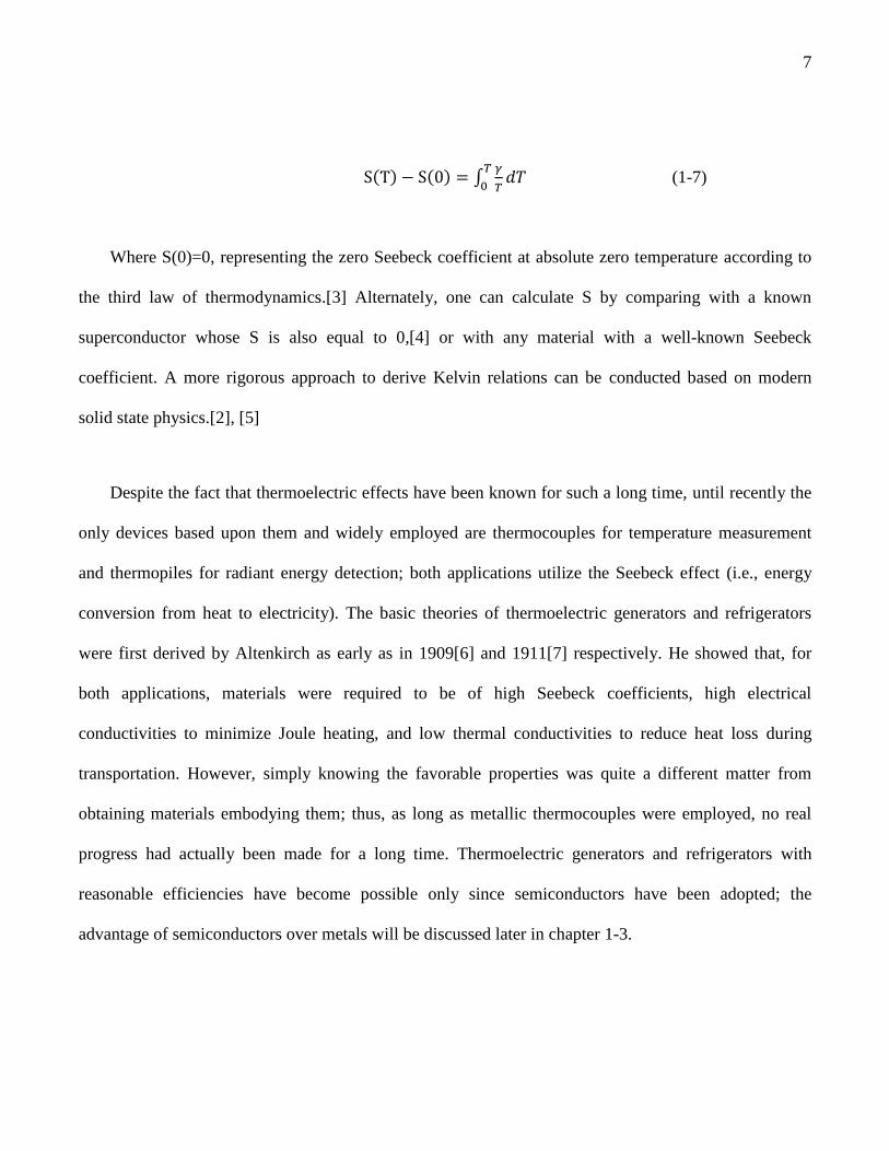
The rate of heat generation/dissipation across each branch is the sum of the Peltier heating in Eqn
(1-2) and the heat conduction term due to temperature gradient dT/dz, explicitly expressed as:
{
(1-8)
With Kelvin relation Eqn (1-5), Eqn (1-8) can then be rewritten as:
{
(1-9)
Where λp and λn represent corresponding thermal conductivities for P and N type branches
respectively. Since current I flows all the way through the module, the Joule heating cannot be neglected;
actually half of the overall Joule heating finds its way to each N-P junction. Here, taking the cold end for
instance, the rate of cooling is composed of the Peltier cooling in both N-type and P-type legs as in Eqn
(1-9), as well as the halved total Joule heating at N-P junction. This can be explicitly stated as:
( )
(1-10)
Where and can be substituted with Eqn (1-9), with boundary condition T(z=0)=Tc,
T(z=L)=Th, Eqn (1-10) can be rewritten as:
( ) ( )
(1-11)

10
Where thermal conductance and electrical resistance are:
{
(1-12)
Thus far, the effective power used to cool the cold sink has been calculated; what follows will be
the total power supplied. Through the whole circuit, part of the potential difference applied to the
module is employed in overcoming the electrical resistances, while the rest is used to balance the
Seebeck voltage resulting from the temperature difference between the junctions. Thus, the external
power supplied W shall be:
( )( ) (1-13)
Based on Eqn (1-11) and Eqn (1-13), the efficiency of this module shall be:
( ) (
)( )
( )( ) (1-14)
The efficiency η as shown depends on the thermoelectric and geometric properties of the two legs,
the temperature difference between two sinks, and the current flow I. As argued by Altenkirch,[6] η
reaches a maximal value when the dimensions of the two legs satisfy the following rule:
(
)
(1-15)

11
Then:
( ) ((
) (
) )
( )
( )
( ) ( ) (1-16)
At this point, it is time to find the optimal IR to maximize efficiency η. IR depends on the electrical
resistance ratio of external loads and the two legs. Letting
( ) , one can find:
( ) ( )
√ (1-17)
Where TM=(Th+Tc)/2, and
((
) (
) ) (1-18)
Z refers to the figure of merit for a certain material or a thermoelectric junction. It should be noted
that, when referring to a thermoelectric material other than a thermocouple or junction, the figure
of merit Z can be rewritten as:
(1-19)

12
Where the thermal conductivity λ consists of electrical (λe) and phonon (lattice) contribution (λl). In
most materials, electrical contribution λe is directly related to the electrical resistivity according to the
Wiedemann-Franz relation:
(1-20)
L0 is the Lorentz number, which is approximately 2.45 x 10⁻⁸
WΩ/K2 for metals and degenerated
semiconductors. Meanwhile, the lattice part is:
(1-21)
C is the specific heat, vs is the sound velocity and lph is the phonon mean free path. Above Debye
temperature, both C and vs are approximately independent of temperature.
Figure of merit Z depends on three parameters – S, σ and λ, all of which are dependent on
temperature and interrelated; thus, it is difficult to optimize all three parameters simultaneously to reach
a maximal Z. In the following chapters, trials of decoupling the interrelation will be introduced as
effective means to improve Z.
Finally, substitute (IR)opt into Eqn (1-16), the relationship between device efficiency η and figure of
merit Z can then be reached:[8]

13
√
√
(1-22)
It is clear that the efficiency η is simply a multiplication of ideal Carnot engine efficiency by a Z
dependent factor (<1); as Z approaches infinity, η draws near to the performance of the ideal
thermodynamic machine.
Presented in Figure 1-5 is the dependence of normalized efficiency ηTE/ηCarnot of an TE engine on
dimensionless figure of merit ZT; not until ZT reaches 3.0~4.0 can the TE engine perform around 50%
as efficiently as the Carnot Engine, which is the typical efficiency of a conventional engine widely used
nowadays. In all of the state-of-the-art TE materials known so far, only the ZT of PbTe series
[9],[10]
,[11] and Bi2Te3 series [12]
,[13] have been reported to be above 1.5, resulting an approximately
35% normalized efficiency.
Figure 1-5 The dependence of normalized efficiency of TE engine on figure of merit ZT.

14
1-3 Semiconductors as optimal thermoelectric materials
As discussed in last section, the efficiency of a TE device is determined mainly by the figure of
merit Z, which is defined as S2σ/λ; hence, an ideal TE material would possess the properties of high
Seebeck coefficient, high electrical conductivity, and low thermal conductivity in the temperature range
of interest. However, these optimal conditions cannot all be met simultaneously, as the enhancement of
one property will always contradict one or both of the others’ benefits. Metals, for example, have half
full conduction bands, no band gaps between conduction and valence bands; these features make metals
ideal charge conductors; unfortunately, metals are also good heat conductors with tremendous thermal
conductivity λ. In addition, in a typical metal, there is no obvious difference in concentration or mobility
between N-type electrons and P-type holes; thus, the heat difference induced currents by N and P type
carriers contradict each other, leading to a very low Seebeck coefficient if any. On the contrary, un-
doped semiconductors and insulators have ideal high Seebeck coefficents and low heat conductivity;
however, they are really poor electrical conductors, due to their extremely low carrier concentrations. As
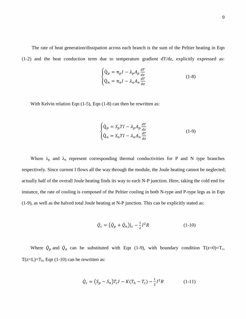
shown in Figure 1-6, the best TE materials are semiconductors doped to certain carrier concentrations,
typically 1019
~1021
/cm3 [14], depending on the operating temperature.
15
Figure 1-6 The dependence of TE properties on carrier concentrations.
For most semiconductors that are not heavily doped, the carrier concentrations are not high enough
to form highly degenerated energy states; at this point, it is convenient to treat them in a non-degenerate
regime with the single band approximation.[15] Also, it should be noted that most good TE materials are
not metallic, rendering it reasonable for us to consider only the majority carrier, either N-type electron or
P-type hole, without worrying about dipolar effects.
Within the single band model, the Seebeck coefficient of a non-degenerate semiconductor is:[15]
16
(
) (1-23)
Where η=EF/kBT is the reduced Fermi energy, and r represents carriers’ scattering mechanism
which is defined as:
(1-24)
Here, τe is the energy dependent relaxation time, τ0 is the carrier’s relaxation time in complete
acoustic lattice scattering case, and E is the carrier energy. The most important scattering in typical
semiconductors are ionized impurity scattering with r=2 and acoustic lattice scattering with r=0.
Assuming the electrical thermal conductivity λe<<λl (the lattice thermal conductivity) in a broad-
band semiconductor, the optimal figure of merit Z can be reached [14] when carrier concentration
satisfies:
( ) (1-25)
Where N(EF) is carrier’s density of state at Fermi level EF.
To evaluate the optimal carrier concentration in non-degenerate semiconductors, some simplified
calculations can be performed: (1) Assuming the carrier’s effective mass m* me, corresponding to
acoustic lattice scattering with r=0 at T=300K, Eqn (1-25) yields nopt ~ 3x10¹⁹
/cm3; while for ionized
impurity scattering with r=2, Eqn (1-25) yields nopt~2x10²⁰
/cm3 at the same temperature. (2) At a higher

17
temperature (e.g., 1273K), however, N(EF) varies with temperature as ~T1.5
, acoustic lattice scattering
with r=0 gives nopt~2x10²⁰
/cm,3 and ionized impurity scattering with r=2 gives nopt~2x10
21/cm.
3
Although the prerequisite of non-degenerate assumption is no longer satisfied at such high carrier
concentrations, the calculations above still provides a simple and straightforward idea what magnitudes
of carrier concentrations are needed to optimize ZT.
The non-degenerate treatment is based on classical free electron theory, which assumes the free
electron gas distributes around the lattice ions and follows the Maxwell-Boltzmann statistics. This
theory has been successfully applied to explain Ohm’s law and have obtained the right order of the
magnitude in electrical resistivity. Nevertheless, the failure for this non-degenerate model to explain
electrical thermal conductivity and other transport properties eventually leads to the development of
degenerate Fermi-Dirac statistics, yielding a dimensionless parameter β, which increases monotonically
with ZT :[16]
(
) (
)
( )
(1-26)
Where μ is carrier mobility, κl the lattice thermal conductivity, m* carrier’s effective mass. The
dependence of ZT on μ, κl and m* strongly suggests materials like “phonon-glass electron-crystal” (low
lattice thermal conductivity κl, high carrier mobility μ) as ideal TE materials.
1-4 State-of- the-art TE materials

18
Figure 1-7 State-of-the-art N-type thermoelectric materials.
Figure 1-8 State-of-the-art P-type thermoelectric materials.

19
In Figure 1-7 and Figure 1-8, the dimensionless figure of merit ZT of both N-type and P-type state-
of-the-art bulk thermoelectric materials are presented. To fabricate thermoelectric devices, different TE
materials are utilized at different operating temperatures in order to achieve decent energy conversion
performance over a wide temperature range.
In the past decade, nanostructure engineering has been introduced to fabricate TE materials and has
then become one of most effective methods to enhance the TE properties. Many traditional state-of-the-
art TE materials with nanostructured features have been reported to achieve significant ZT
improvements in comparison with their bulk forms.[12], [17], [18] Nanostructures introduced into bulk
TE materials not only serve as phonon-particle scattering centers but are also capable of inducing the so-
called energy filtering effect,[19],[20] both of which help to decouple the firmly interrelated thermal and
electrical transport properties, eventually making it possible to suppress the lattice thermal conductivity
and enhance the power factor (PF=S2/ρ) simultaneously. Table 1-1 shows direct comparisons of ZT and
thermal conductivities between nanostructured TE materials and their traditional bulk counterparts.
Table 1-1 Thermoelectric properties of nanostructured materials at optimal operation temperatures,
values in the parentheses correspond to their conventional bulk types.

20
composites carrier type
thermal
conductivity(W/m/K)
ZT Ref.
Si80Ge20Bx ( ) 0.95(0.5) at 800-900 [21]
Si80Ge20P2 ( ) 1.3(0.93) at 900 [17]
(Bi,Sb)2Te3 ( ) 1.4(1.0) at 100 [12]
(Bi,Sb)2Te3 ( ) 1.3(1.0) at 75-100 [22]
(Bi,Sb)2(Te,Se)3 0.7-0.9 at RT [23]
Bi2(Te,Se)3 0.5 at RT [24]
Co4Sb12 ( ) 0.05 at RT [25]
Yb0.35Co4Sb12 1.2 at 550 [24]
(Ni0.09Co0.91)4Sb12 0.75 at RT [26]
Mg2Si0.4Sn0.6 0.13 at 653K [27]
Mg2Si0.6Ge0.4 0.21 at 610K [28]

21
Hf0.6Zr0.4NiSn0.995Sb0.005 ( ) 1.0(0.8) at 850K -
Hf0.6Zr0.4NiSn0.99Sb0.01 4.4(5.8) 1.0(0.75) at 600 [29]
Hf0.5Zr0.5CoSn0.2Sb0.8 3.25(4.85) 0.8(0.5) at 700 [18]
2atm%ZrO2+Hf0.3Zr0.7CoSn0.3Sb0.7 3.3(3.6) 0.8(0.65) at 700 [30]
As discussed in chapter 1-3, a good candidate for thermoelectric applications should have a low
lattice thermal conductivity, a high carrier mobility, and a large carrier effective mass. Normally, a
broad-band semiconductor own a high Seebeck coefficient at high temperatures, complex unit cell and
heavy atoms always assure low lattice thermal conductivities. Meanwhile, the candidate has to be
susceptible to proper carrier doping to reach the optimal carrier concentration. Moreover, a highly
symmetric lattice structure indicates a greater degeneracy of energy states and thus helps to improve the
Seebeck coefficient.
Other than thermoelectric performance, to be qualified in device fabrication and future commercial
promotion, a thermoelectric candidate also has to be:
(1) Thermally stable at the operating temperatures, which limits the applications of Sb-rich
skutterudites.

22
(2) Non-toxic, unlike arsenides, tellurides and selenides.
(3) Susceptible to both N-type and P-type doping, with comparable thermoelectric performance.
(4) Low-cost.
Half Heusler alloys and Silicon Gemernides, as will be discussed in later chapters, are decent
candidates that satisfy most of the requirements mentioned above.
1-5 Motivation
As the conflict between the growing demands for energy and the limited reserves of non-renewable
fossil fuels (e.g., oil, natural gas, coal) has grown more severe over the years, meanwhile, the
environmental impact of global climate change due to the combustion of fossil fuels is becoming
increasingly alarming, therefore, research into alternative and renewable energy has become a key
priority. One way to improve the sustainability of electricity bases is by recycling waste heat with
thermoelectric generators. Many kinds of heat are wasted in our everyday life, among them, wasted heat
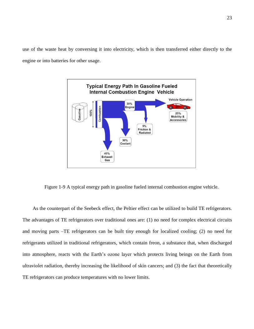
from automobiles is especially representative, as shown in Figure 1-9. It is surprising that only 25% of
the energy from fuel goes into the useful portion as vehicle’s kinetic energy, while around 75% is
discharged as waste heat, either by heating up coolant or through exhaust gas. TE generators can make
23
use of the waste heat by conversing it into electricity, which is then transferred either directly to the
engine or into batteries for other usage.
Figure 1-9 A typical energy path in gasoline fueled internal combustion engine vehicle.
As the counterpart of the Seebeck effect, the Peltier effect can be utilized to build TE refrigerators.
The advantages of TE refrigerators over traditional ones are: (1) no need for complex electrical circuits
and moving parts –TE refrigerators can be built tiny enough for localized cooling; (2) no need for
refrigerants utilized in traditional refrigerators, which contain freon, a substance that, when discharged
into atmosphere, reacts with the Earth’s ozone layer which protects living beings on the Earth from
ultraviolet radiation, thereby increasing the likelihood of skin cancers; and (3) the fact that theoretically
TE refrigerators can produce temperatures with no lower limits.

24
To date, the most effective TE devices can generate electric power or absorb heat at 10% of the
Carnot efficiency, whereas traditional refrigerators generally operate between 30% and 90% of the
Carnot efficiency for most consumer appliances and large-scale industrial machinery respectively. The
substantial drawback of this lack of efficiency has limited the world market for thermoelectric devices to
about $80-160 million annually, notwithstanding their low cost and high reliability.[31] Today, most of
these devices are used to cool laser diodes or are sold as novelty consumer appliances. Despite the
somewhat disappointing performance of current thermoelectric technologies, in general the efficiency of
these TE devices has no known limit short of the Carnot efficiency,[14] which warrants further research
in this field.

25
2. Sample synthesis and characterization
2-1 Sample synthesis
2-1-1 Arc melting
Arc melting is a widely used method to synthesize bulk composites with high melting points. High
purity element pieces are melted together under argon atmosphere into button-shaped bulk ingots by
induced high power electric arc. Most of the elements used in our alloy synthesis are ordered from Alfa
Aesar and Sigma Aldrich; normally, a purity of 99.5% or higher is required to minimize impurities. The
arc melting chamber is pumped down to 30 mTorr, and backfilled with argon to ambient pressure; the
argon is used to provide a protecting atmosphere during arc melting process. A water-cooled thoriated
tungsten electrode is typically used for high voltage arcing generation. During the melting process, a
piece of Zirconium is first melted to exhaust residual oxygen before intended compositions are to be
alloyed. It should be noted that the raw ingot obtained after first melt needs to be flipped and melted a
couple of more times to allow for thorough alloying and to minimize inhomogeneity.
Two noteworthy techniques to arc melt Half Heusler alloys are as follows:
(1) Sb(antimony) is a metalloid with a low sublimation point. To count for the sublimation/loss of
Sb during arc melting, additional 5% antimony is strongly suggested when synthesizing Sb rich alloys
XCoSb(X=Hf,Zr,Ti). This method is proven to be necessary to obtain the intended composites.

26
(2)A tiny amount of Sb is typically added into XNiSn (X=Hf, Zr, Ti) as an N-type dopant; however,
due to the low sublimation point of Sb element, any slight Sb loss during melting would lead to a
significant deviation of carrier concentration from nominate composite. One technique to solve this
problem is to make a Sn-Sb precursor with a MAPP gas torch, since the Sn-Sb solid solution has a much
higher sublimation point than Sb. To do so, Sn and Sb pieces with a 10:1 atomic ratio are loaded into a
quartz tube, which is then evacuated down to 10 mTorr with a two-phase pumping system (a roughing
pump plus a diffusion pump). Sn-Sb pieces are then sealed in the quartz tube with a Hydrogen-Oxygen
torch. Thereafter, a MAPP gas torch is used to melt Sn and Sb together homogenously. It is worth
pointing out that MAPP gas is used due to its mild flame temperature, which is incapable of melting
quartz but high enough to melt Sn and Sb.
2-1-2 Annealing
Arc melted ingots are water-cooled from above 2000 down to room temperature in around 10
seconds, this fast cooling process normally results in residual stresses, inhomogeneity, impurity phases
and crystal defects, all of which can significantly affect TE materials’ performance; hence, post
annealing is necessary to obtain a TE ingot that is homogenous and has a stable TE performance for
extended time at elevated temperatures. To prepare for annealing, a TE ingot is wrapped with a piece of
tantalum foil and loaded into a piece of quartz tube. The quartz tube is then evacuated down to 10 mTorr
and sealed with a Hydrogen-Oxygen torch. The sealed quartz tube is then heat treated in a high
temperature furnace following a specific recipe. Taking a N-type Half Heusler alloy for example, the
sealed quartz tube normally sits at 900 for one day to obtain homogeneity, and then at 800 for 7 to

27
10 days for phase stabilization. The quartz tube is then quenched in water to retain the sample’s high
temperature phase.
2-1-3 Induction melting
Metallic alloys can also be synthesized through induction melting by induced Eddy currents; for
materials that are too resistive to generate Eddy currents, conductive graphite crucibles are normally
used for assistance. With the metallic sample or subsidiary graphite crucible being seat in the middle of
a piece of copper coils, a high frequency AC then runs through the copper coils, inducing an high
frequency alternating electric-magnetic field, which then induces an alternating electric field in either
the sample or the graphite crucible; the electric filed induced Eddy current is very powerful that the
sample can be heated up and melted within seconds. Induction melting is specifically useful to melt
powder pellets or elemental pieces with low melting points, which otherwise are hard to be synthesized
via direct arc melting.
2-1-4 Solid State Reaction
Neither arc melting nor induction melting is able to perform an alloying process with temperature
precisely controlled. Dissimilarly, solid state reaction (SSR) (sometimes called solventless reaction or
dry media reaction) which is a chemical reaction in the absence of a solvent, is occasionally used to
synthesize composites with low melting points or whose reaction processes need to be well controlled to
avoid dangerous situations like explosions. For instance, Fe3P can be synthesized using the following
recipe:

28
(1) Stoichiometric Fe and red phosphorous powders are weighed out and ball mixed in a stainless
steel vessel for 40 min to allow sufficient mixing.
(2) The powder mixture is compressed into a cylindrical pellet with an arbor press.
(3) The compressed pellet is then loaded into a piece of quartz tube.
(4) The quartz tube is evacuated with a two-phase pumping system down to 10 mTorr and sealed
with a Hydrogen-Oxygen torch.
(5) Finally, the quartz tube is heat treated in a relatively slow and cautious way as following:
Stays at 100 for 1 hour
Stays at 150 for 1 hour
Stays at 200 overnight and one day to allow sufficient reaction of P with Fe
Stays at 250 for 2 hours
Stays at 300 for 2 hours
Stays at 350 overnight

29
Stays at 400 for 2 hours
Stays at 500 , 600 , 700 , 800 for 1 hour each
Finally stays at 900 overnight
(6) The quartz tube is cooled in air slowly down to room temperature. Goggles are strictly required
when the cooled quartz tube is broken, in order to avoid possible explosion due to the outgassing during
heat treat process.
2-1-5 Melt spinning
Melt spinning is a technique used to perform rapid cooling in order to obtain amorphous or near
amorphous microstructures. A thin stream of melted liquid solution is dripped onto the surface of a
rapidly rotating water-cooled copper wheel, resulting in fast solidification. The cooling rate that can be
achieved by melt-spinning is between 104~10
7 K/s. Although it is hard to obtained amorphous TE
materials with this method, ribbons with nano-scaled features were still achievable for Half Heusler,[32]
Bi2Te3[33] and Si-Ge[34].
Fractures of homogenously arc melted alloy are loaded into a piece of quartz tube, whose bottom
end has been fused into a 0.5mm diameter hole. The quartz tube is then placed right through the center
of water-cooled copper coils, and several millimeters above the water-cooled copper wheel. Next, the
rotating rate of the copper wheel (typically 3000 rps or round/s) is carefully adjusted, with an AC current
30
running through the copper coils, the alloy fractures are liquefied and injected out of the quartz tube onto
the copper wheel for fast consolidation. The obtained ribbons with nano-sized grains can thus be
compressed into bulk form using Spark Plasma Sintering (SPS) or Hot Press (HP) method.
2-1-6 Ball Milling
In addition to melt spinning, ball milling-a powerful mechanical grinding and alloying technique -is
also widely used to obtain nano-sized powders. The materials of ball milling vessels and grinding balls
have to be carefully chosen to avoid mutual contaminations with TE alloys. Surfactants are also widely
used to avoid over-alloying. There are experience rules that the mass ratio of balls to samples has to be
between 6:1 and 8:1, and that the quantity ratio of ball size of 0.25” to that of 0.125” has to be between
1:2 and 1:4, depending on sample compositions.
To start, 10 grams of hand ground Half Heusler raw powders or element powders of Si and Ge, as
well as grinding balls, are loaded into a pre-cleaned stainless steel vessel; two of these balls are 0.25” in
diameter, while the rest four are 0.125” in diameter. The sealed vessel is then fixed in position in the
SPEX Dual ball miller 8000D, which is seated in an aluminum box. The aluminum box is then
evacuated and backfilled with argon to provide a protecting atmosphere during the ball milling process.
Ball milling process usually takes 5 to 10 hours, and the size of obtained particles fall in the range from
20nm to 50nm. The nanopowders can then be consolidated into bulk form with Spark Plasma Sintering
(SPS) or Hot Press (HP) technique. Significant grain growth may happen during the SPS or HP process.

31
SPS is believed to have less grain growth in the sense that the heating/cooling rate of SPS is much faster
than its competitor HP.
2-1-7 Spark Plasma Sintering
Spark Plasma Sintering (SPS), also known as field assisted sintering technique (FAST)[35] or
pulsed electrical current sintering (PECS), is a powerful sintering technique. The main characteristic of
SPS is that the pulsed DC current (typically over 500 A) is directly passing through the graphite die as
well as the compacted powder layer; therefore, the heat is generated internally, in contrast to
conventional hot pressing (HP), where the heat is transported into the intended powder layer from
external hot sink. This internal heating mechanism facilitates a very high heating or cooling rate (up to
1000 K/min); hence, the sintering process is generally very fast (within a few minutes). The rapid
heating speed ensures that SPS has the potential to densify the nano-sized powders while avoid the
significant grain growth which accompanies standard densification routes. While the term “spark plasma
sintering” is commonly used, this term is misleading, since neither a spark nor any plasma is present in
the SPS process.[35] It has been experimentally verified that densification is facilitated by the use of a
tremendous direct current.
Model 10-4 SPS, a Thermal Technology LLC product, is composed of three main parts: a DC
power supply, a hydraulic compressing system and an operation chamber. Fine powders are loaded into
a graphite die of 2cm in diameter and sandwiched by a pair of graphite punches. Thin graphite foils are
placed between the graphite punches and the compacted powder layer, as well as between the graphite

32
die and the compacted powder layer, so as to avoid mutual contamination between sample and die. The
graphite die is then wrapped by a few layers of graphite fur, in order to minimize heat loss during the
heating process so as to maximize the heating rate. The “coated” graphite die is then sandwiched
between two graphite blocks before being inserted into upper and lower stainless steel rams which are
driven by the hydraulic pump. The temperature of the upper and lower rams can be read from the
attached thermal couples. It should be noted that the temperature of either of the rams should not exceed
650 for safety reasons; thus, the system is programmed so that once either ram reaches this
temperature limit, the whole program will be aborted and the power supply will be cut off immediately.
The temperature of the compacted powder layer can be monitored by two independent systems: if the
max operation temperature is below 1000 , a third thermal couple is attached with the lower punch;
otherwise, an infrared pyrometer is adopted to read corresponding temperatures.
The compressing chamber is evacuated to or below a setting pressure of 20 mTorr and then
backfilled with an inert gas like argon or helium. This backfilling process will be automatically stopped
once the pressure in the chamber exceeds the atmosphere pressure. The hydraulic pump-driven rams and
the operation chamber are water-cooled during the whole SPS process, and an automatic warning system
is also implemented in the water-cooling system. The SPS process (temperature, pressure and holding
time) can be pre-programmed using a software program called iTools. The recommended maximal
heating rate is 300 K/min, and the ramp rate of pressure is 60 MPa/min. The maximal weight provided
by the hydraulic pump is around 10 tons, for a die with inner diameter of 20 mm, the corresponding
maximal pressure shall be around 300 MPa. Once the pre-set program is turned on, corresponding SPS
parameters can then be read from a software program called SpecView. When the SPS process is done,

33
allow around 30 minutes for the graphite die and the rams to be water cooled down to room temperature.
Normally, the sample obtained is covered by the protecting graphite foils, thus, successive polishing
must be performed before the sample can be characterized.
2-1-8 Sample preparation for SEM
Samples in both powder and bulk form can be examined under SEM. For powders, 2 to 3 mg
powders are evenly spread on one side of a piece of double-side adhesive, with the other side sticking to
an aluminum supporting platform ready for SEM scan. For bulk samples, two options are provided. If
morphology of the cross section is to be studied, one may simply crack the bulk into smaller pieces and
select one piece with a relatively flat cross section. Or, if grain boundaries and impurity grains are of
more interest, fine polishing and surface etching are thus necessary. In this case, the bulk sample is
polished with SiC sandpapers in mesh sizes of 300, 800, 1200 and 4000 successively, until the surface
becomes mirror-smooth; finer polishing is then performed on a polishing fur with corresponding
polishing additives ( turbid liquids containing micron-sized Al2C3 particles). Next, the sample is cleaned
in an ultrasonic vibrator to “shake off” residual Al2C3 and SiC particles. After being cleaned, the sample
needs to be etched with proper etchant to reveal the surface grains; for HH alloys, the etchant is
composed of 4 parts 100% acetic acid, 4 parts 70% nitric acid, and 2 parts 50% hydrofluoric acid. This
etchant is applied to the polished surface of the sample, which is then exposed to air for 15 seconds to
allow for a sufficient chemical reaction before the surface being cleaned with distilled water.

34
2-1-9 Sample preparation for TEM
(1) Powders
Powders of approximately 2 to 3 mg are mixed into 100ml alcohol; the turbid liquid is then stirred
for 5 minutes to allow for thorough mixing. A veco center reference grid (copper) with 400+ mesh (a
TED PELLA product) is then dipped into the turbid liquid for 5 seconds; afterwards, the grid is covered
by a piece of wax paper and allow air dry.
(2) Bulk samples
Polishing: A piece of bulk sample about 5mm x 5mm in size is polished using the method
described in section 2-1-8 to a thickness around 150μm.
Dimpling: The sample is stuck on to a TED PELLA designed Cu aperture grid with a 2mm
diameter inner hole; it is necessary to tailor the size of the sample so as not to exceed the outer edge of
the Cu grid. The Model 200 Fischione Instruments Dimpling Grinder is used to thin the sample to the
point that the thinnest part is eventually in the range of 20 to 30μm.
Ion milling: The sample, with its Cu grid base, is fixed on a rotating support platform in the ion
mill chamber, which is then evacuated to 10-4
Torr. One should adjust the left emission gun to 10 on
top of the sample and the right emission gun to 10 below the sample to maximize the ion mill rate.
After charging, argon atoms are ionized and accelerated in the electrical field before they bombard onto

35
the rotating sample. This ion mill process is continued until a hole appears at the center of the dimpled
sample. Adjust the both left and right guns to 4 , and perform another 15 minutes ion mill to make the
edge around the hole thinner. TEM examination will be focused on the edge around the hole, because
only this region is thin enough for the transmission of electrons.
2-2 Sample characterization
2-2-1 X-Ray Diffraction
Powder X-Ray Diffraction (XRD) can be used to identify crystalline phases and to trace the changes
on lattice constant due to doping level. A piece of alloy is smashed with a hammer and hand ground into
micron-sized powders with mortar and pestle. Obtained powders are then spread on top of a piece of
single crystal substrate, which is utilized to minimize the background signals. Diffracted beam adopts a
Ni beta-filter and a 0.04rad soller slit. Usually, the scanning range is from diffraction angle 2θ =20 to
2θ=80 , although this may be adjusted if necessary. The diffraction patterns obtained are then compared
with the database to identify the crystal structures, and possible composites.
It worth nothing that XRD peaks can also be utilized to estimate crystallite size, which will be
introduced in detail in chapter 4.
36
2-2-2 Atomic Force Microscopy
Atomic force microscopy (AFM), also called dynamic force microscopy (DFM), is a scanning
probe microscopy of very high resolution. Its main component is a piezoelectric feedback loop, which is
used to keep a constant tip-sample interaction, the interaction signal in return can be used to adjust the
height of the tip above the sample surface. A Nanosurf easyScan dynamic force microscopy is used for
surface scanning of well-polished and etched samples and for grain-size determination by a silicon
cantilever that is 228μm in length. This DFM can be operated in three modes:
(1) Static force mode
A laser beam deflection system with an 830nm characteristic wavelength and an 0.4mW operation
power is used to measure the bending of the cantilever. The deflected laser is then gathered by array of
photodiodes for imaging.
(2) Dynamic force mode
The cantilever is oscillated at a pre-set amplitude and at a frequency near its resonance by a piezo
element. Any change on the tip-sample forces will alter the resonance frequency of the cantilever,
thereby inversely altering the oscillating amplitude, which is measured by the laser deflection system.
(3) Phase contrast mode

37
This mode is essentially an enforced dynamic force mode. In addition to the oscillation amplitude,
the oscillation phase of the cantilever is also monitored, providing information regarding the relative
stiffness of the sample surface under the tip; hence, this mode is used primarily to detect possible
nanosized minor phases in the main matrix.
The scan area of AFM can be as large as 10μm by 10μm, and the characteristic features as small as
20~30nm can be resolved.
2-2-3 “Homemade” high temperature probe
The Seebeck coefficient and electrical resistivity can be measured simultaneously using a
homemade HT probe up to 1100K, the probe’s schematic structure is sketched in Figure 2-1.
Figure 2-1 A schematic “homemade” high temperature thermoelectric probe.
38
A sample to be measured is cut into a rectangular piece of 10mm x 4mm x 4mm before being
inserted between two silver blocks. External pressures are then applied on both sides to make sure that
the sample tightly sticks against the silver blocks so as to provide reliable thermal and electrical contacts.
In a typical resistance measurement loop, constant DC current I (10-3
A) runs into one silver block,
through the sample, and out from the other silver block. Voltage ΔV, across a pre-measured distance
along the sample, is measured. Resistivity can then be derived from this well-known four-point
resistance measurement method, which was first proposed by Lord Kelvin in 1861:
(2-1)
Where ρ is the electrical resistivity, l is the distance between the two voltage leads, S is sample’s
cross section. In a typical Seebeck coefficient measurement loop, a heater strip is used to heat up the hot
sink, temperature Th of hot end is then read by thermocouple 1, while Tc of the cold end is read by
thermocouple 2. The Seebeck voltage ΔVs, induced by the temperature difference ΔT=Th-Tc, is read by
the DC current leads. Note that ΔVs also receives a contribution from the silver blocks; to calcuate the
net Seebeck coefficient of the sample, one has to subtract the thermopower of silver-SAg from total
Seebeck Vs/ T, SAg is given by an experience formula as:
SAg = 0.97153 - 0.0018878T + 1.3617E-5 T2
- 4.7322E-9 T3 (2-2)
Other than the data acquisition probe described above, the measuring circuit also contains a
Keithley 220 precision current source, a Keithley 2182 nanovoltmeter, a Keithley 7001 control system

39
and an Agilent E3642A DC power supply. This system of data acquisition and analysis circuit was
programmed by S. R. Culp via Labview, as outlined in his PhD thesis.[36]
Despite this HT probe’s moderate performance, the drawbacks listed below make it necessary to
find a replacement.
(1) Both the DC current supply loop and the temperature acquisition loop are wired with silver
strings of 0.25mm in diameter, which are extremely brittle in light of the possibility of external force
and high temperature “baking” during the measuring process.
(2) Two tiny Ni-Cr wires are attached to the sample as voltage leads via silver paint, however, this
sort of attachment is unstable and always cause loose electric contacts during measurements.
(3) The probe necessitates frequent refurbishment to get rid of residual contaminants which may
lead to short circuits.
(4) It is hard to obtain a steady state temperature at which the Seebeck coefficient can be measured,
since the heating unit of the whole probe and the heater strip attached with the hot sink are controlled
independently.
40
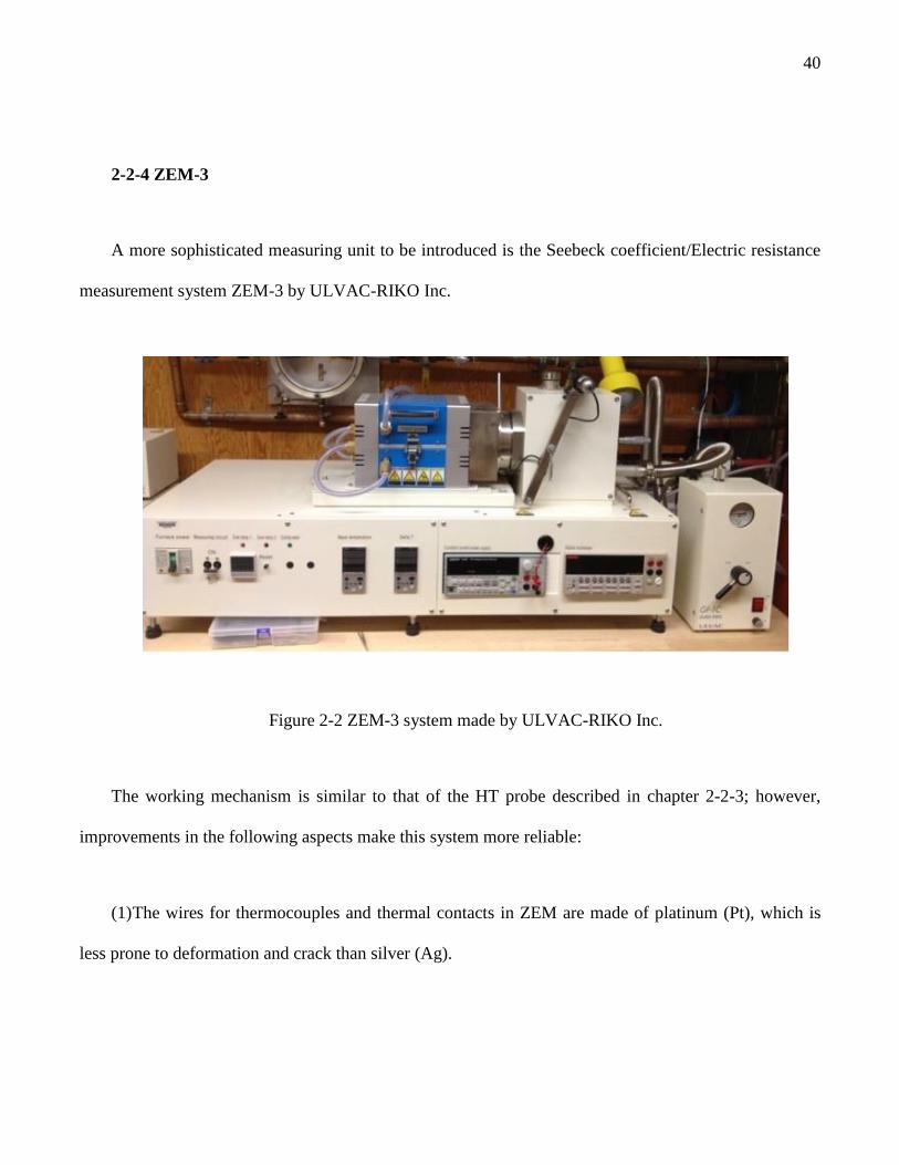
2-2-4 ZEM-3
A more sophisticated measuring unit to be introduced is the Seebeck coefficient/Electric resistance
measurement system ZEM-3 by ULVAC-RIKO Inc.
Figure 2-2 ZEM-3 system made by ULVAC-RIKO Inc.
The working mechanism is similar to that of the HT probe described in chapter 2-2-3; however,
improvements in the following aspects make this system more reliable:
(1) The wires for thermocouples and thermal contacts in ZEM are made of platinum (Pt), which is
less prone to deformation and crack than silver (Ag).
41
(2) The operation chamber holding the probe can be evacuated to 10 mTorr in a couple of minutes
and backfilled with protecting gas, thus refurbishment is no longer necessary; it also has a built-in relief
valve for safety reasons.
(3) Thermal and electrical contacts are ensured by both vertical and horizontal external pressure.
(4) The heating unit of the chamber coordinates well with the heater strip attached with the hot sink,
ensuring a steady state temperature at any measuring point.
2-2-5 Thermal conductivity
The pulse or laser flash method to determine thermal conductivity was first described by Parker et
al.[37] in 1961; since its inception, approximately more than 75% of all thermal diffusivity results
published in the primary scientific literature[38] after the 1970s have been obtained using this single
technique. A Netzsch LFA 457 MicroFlash system is used to perform laser flash thermal conductivity
measurements. One surface of a disc-shaped sample (dimensions 1/2” x 1/2” x 1/10”) is irradiated by a
short (less than 1ms) laser pulse. The resultant temperature T on the opposite surface is recorded; the
thermal diffusivity δ can then be computed from T vs. time data:
(2-4)
42
Where L is the diameter of the disc-shaped sample, and t1/2 is the time taken for the temperature on
the rear surface to reduce to half its maximum value. This technique relies on the fulfillment of
relatively stringent boundary conditions,[16] namely:
(1) The pulse of energy is uniformly absorbed in a small depth at the surface x=0,
(2) The heat pulse dissipation time is of negligible duration, and
(3) The measurement time is sufficiently short so that no loss of heat occurs from the sample.
As long as thermal diffusivity is determined, the thermal conductivity can be calculated via:
λ = Cp ρ (2-4)
Mass density ρ is measured via classical Archimedes method, and specific heat Cp is measured by a
Netzsch LFA Differential Scanning Calorimeter (DSC). The DSC technique was developed by Watson
and O’Neill in 1962 and introduced commercially at the 1963 Pittsburgh Conference on Analytical
Chemistry and Applied Spectroscopy. The first adiabatic differential scanning calorimeter usable in
biochemistry was developed by Privalov and Monaselidze in 1964.[39] During a measurement,
intended sample and reference material of equal weight are maintained at nearly the same temperature
throughout the experiment. The temperature program for a DSC analysis is designed such that the
sample holder’s temperature increases linearly as a function of time. Since the reference material has a
well-defined heat capacity over the range of temperatures to be scanned, provided the difference in
43
required heat to maintain the intended and reference samples at the same temperature, one can then
determine the intended sample’s heat capacity.
2-2-6 Hall Effect
Hall effect was discovered by Edwin Hall in 1879. The process can be described as follows: when a
current is passing through a conductor in a perpendicular magnetic field, the charge carriers constituting
the current will accumulate in the direction transverse to both the direction of the current flow and the
direction of the applied magnetic field, due to the Lorentz force; the process eventually will arrive at
equilibrium when the induced electric field due to carriers’ accumulation can completely balance the
effect of the Lorentz force. This induced electric field is named the Hall voltage VH, and the ratio of Hall
voltage to the product of the current density and the magnetic field is called Hall coefficient. The Hall
coefficient is a characteristic property of the conductor, which reveals carrier’s type and density as
follows:
(2-5)
Where t is the thickness of the conductor in the direction of magnetic field.
A VersaLab, 3 Tesla, Cryogen-free Vibrating Sample Magnetometer (VSM) is used to conduct the
Hall effect measurement. This VSM has a sensitivity of 10-6
emu/rt-Hz, a characteristic maximal
magnetic field up to 3 Tesla, and an operating temperature ranging from 50 to 400K. In our case, a

44
carefully polished rectangular sample is mounted on a sample holder, the electrical joints of which are
then wired with two ends and two perpendicular sides of the sample, forming a typical four-point
resistance measuring circuit. The electrical connections between wires and leads are soldered by Indium.
The magnetic field is applied in the direction perpendicular to the sample holder. The electrical leads on
the two ends of the sample are used as current supply and the other two on the sides are used to record
the induced Hall voltage. In a typical measuring loop, current flow I is kept constant, as the magnetic
field varies, corresponding Hall resistances rH=VH/I are automatically recorded. For non-magnetic
materials, the outcome is a linear dependence of Hall resistance rH on the applied magnetic field B; the
slope is then expressed as L=rH/B=VH/IB=-1/net. With carrier density n=-1/etL being calculated, the
carrier mobility is then derived as follows:
(2-6)
45
3. Thermoelectric properties improvement on Half Heusler alloys via
nanostructuring
Half Heusler (HH) alloys of MNiSn and MCoSb (M=Hf, Zr, Ti) types are well-studied TE materials
with decent performances at high temperatures ranging from 700K to 1100K;[40],[41] in addition, they
are low-cost and non-toxic. The thermoelectric performance of Half Heusler alloys is mainly limited by
their comparably high thermal conductivity. This chapter will focus on how to improve the thermopower
and reduce the lattice thermal conductivity. Through introducing localized impurity states, the density of
states (DOS) of host at the Fermi level can be significantly increased over a narrow range, forming so-
called resonant states, which can greatly enhance the Seebeck coefficient according to the Mahan-Sofo
theory.[42] Mechanical alloying/ball milling is adopted to implement nanostructured features into state-
of-the-art bulk HH, not only leading to a reduction in thermal conductivity by the much more intense
interface scattering at grain boundaries, but also resulting in low energy carriers that are detrimental to
thermopower being trapped at grain boundaries, eventually an improvement in the Seebeck coefficient.
The work in this chapter has been published in by J. W. Simonson, D. Wu et al. in Phys. Rev. B 83
(2011) 235211 and by S. J. Poon and D. Wu et al. in Journal of Materials Research 26 (2011) 22.

46
3-1 Introduction of Half Heusler (HH) alloys
The crystal structure of HH alloys is a face centered cubic (FCC). For example, in MNiSn, the
transition metal M (M=Hf,Zr,Ti) atoms and Sn atoms form a rock salt (NaCl) frame, with four Ni atoms
filling half of the eight quadrants, as shown in Figure 3-1. This is also the origin of the term “Half
Heusler”, compared with “Full Heusler” in which all eight quadrants are occupied.
Figure 3-1 Crystal structure of MNiSn (M=Hf, Zr, Ti) Half Heusler phase.
Undoped intrinsic Half Heusler alloys express semiconducting properties, as their valence electron
count (VEC) is equal to 8 or 18, and the band gap for typical MNiSn/MCoSb (M=Hf, Zr, Ti) lies in the
range of 0.5~0.8 eV. The origin of the band gap in Half Heusler is still unclear; calculations via first
principles show that it either comes from the combination effect of M-3d – Sn-4p strong hybridization

47
and Ni-3d orbitals indirectly mediating the interaction between the M-dxy orbitals and hybridized M-3d –
Sn-4p[43], [44] or comes from the d-d repulsion between Ni-3d orbitals and strongly hybridized M-3d –
Sn-4p.[45] In either case, the conduction band edge is predominated by M-3d character, while the
valence band edge is predominated by Ni-3d orbitals.
Although high Seebeck coefficients were observed in intrinsic MNiSn/MCoSb,[45], [46], [47] the
relatively low electrical conductivities result in insufficient Power Factors (PF=S2σ) for any actual
applications. The Power Factors of intrinsic Half Heusler alloys can be greatly improved by proper
doping on the Sn/Sb site, as has been shown in many works.[36], [40], [41] Further enhancement in the
Seebeck coefficient can be achieved with band structure engineering – specifically, increasing the local
density of states (DOS) at the Fermi level by introducing localized impurities to the matrix material.
Additionally, low energy carriers are found to be detrimental to thermopower, as discussed theoretically
and experimentally by Shakouri et al.,[48] their finding further indicates that preferentially scattering
low energy carriers via energy barriers can result in an enhanced Seebeck coefficient.
It has also been well presented that the thermal conductivity can be reduced by over 50% through
introducing isoelectronic elements, specifically Hf1-x-yZrxTiyN(N=Ni,Co)S(S=Sn,Sb),[49], [50] without
compromising the Power Factor.[41][51] The dramatic reduction of thermal conductivity is attributed to
mass fluctuation effect/point defect scattering-phonon transport is impeded by the strain field fluctuation.
A widely used model to evaluate point defect scattering is the Klemens-Drabble theory.[50], [52]
Moreover, nanostructuring techniques have also shown great promise of achieving high ZT[18], [32],
[53], [54], [55], [56] by significantly reducing thermal conductivity; in some cases, they can result in
48
Power Factor PF(=S2σ) enhancement.[9], [13] The mechanism of nanostructuring is understandable in
the sense that interfaces intensity among embedded nanoparticles and matrix materials is significantly
increased, these interfaces act as both thermal barriers and scattering centers of acoustic phonons,[14],
[15], [16] as well as energy filterers for charge carriers, resulting in the reduction of thermal
conductivity and the enhancement of thermopower.[32], [57]
3-2 Resonant states
3-2-1 Background
In most semiconductors, the addition of doping atoms results in extra impurity states in the band
gap. When these states are close to valence (conduction) band edges, the holes (electrons) in the
impurity states will tend to be thermally activated into the valence (conduction) band and thereby lead to
an increase of carrier concentration. There is also an exception to this mechanism; specifically, when the
impurity states introduced by dopants lie in the valence or conduction band edge, a localized increase of
density of states over a narrow energy range may be formed due to the strong hybridization between the
impurity states and matrix band, forming so-called resonant states, as shown in Figure 3-2. The theory of
localization of DOS was well studied in the GaAs1-xNx system by Wu et al.[58] and in the ZnSe1-xOx
system by Lee et al.[59] A remarkable increase in the Seebeck coefficient, and therefore ZT, was also
observed in a state-of-the-art PbTe system with 2% Tl doping on the Pb site by Heremans et al.[9]

49
Figure 3-2 Localized resonant states over a narrow energy range ER at Fermi level.
The mechanism of enhancement of the Seebeck coefficient by localized DOS increase at the Fermi
level can be expressed using the Mott expression[60] as follows:
( ( ))
|
{
( )
|
( )
|
} (3-1)
With the differential electrical conductivity σ expressed as:
( ) ( ) ( ) (3-2)

50
Where carrier concentration n(E)=g(E)f(E) is the product of DOS g(E) and Fermi distribution
function f(E) at E, μ(E) is the energy dependent carrier mobility. From Eqn (3-1), an enhanced Seebeck
coefficient can be expected, if the Fermi level lies where DOS g(E) (and therefore n(E)) is experiencing
a steep change.
3-2-2 Experiments
Polycrystalline Half Heusler alloys of nominal compositions (Hf0.75Zr0.25)1-xVxNiSn with x=0%,
0.25%, 0.5% and 1.0% were arc melted 3~4 times to allow for homogeneity, and the mass losses during
arc melting processes were strictly controlled under 0.5%. The purities of the commercially available
elements Hf, Zr, V, Ni and Sn are 99.7%, 99.95%, 99.7%, 99.98% and 99.99%, respectively. The as-
casted ingots were then sealed in quartz tubes under vacuum for post-annealing, the details of which
were described in chapter 2-1-2. The post-annealing recipe is at 900 for 1 day, and 800 for 7 days.
Post-annealing was performed in order to allow for strain release and crystal growth via thorough
diffusion. The existence of the Half Heusler phase was then identified by XRD diffraction, and
homogeneity was verified via Energy Dispersive Spectroscopy (EDS) line scan (Figure 3-3) over a well-
polished sample, as presented in our published work.[61]

51
Figure 3-3 (a) Powder XRD scan (b) SEM image of surface micrograph and (c) EDS line scan of
(Hf0.75Zr0.25)0.99V0.01NiSn along the yellow arrow in (b).
The actual chemical compositions of V doped HH alloys were determined by EPMA (Electron
Probe Microanalyzer) with 50 ppm detection limit. The atomic percentages of V were found to be 0.24%,
0.63% and 0.78%, somewhat deviating from the nominal 0.25%, 0.50% and 1.0%; nevertheless, the
increasing trend of V content in (Hf0.75Zr0.25)1-xVxNiSn was still retained.
Thermopower and electrical resistivity from RT (300K) to 1083K were measured with a home-built
high temperature thermoelectric probe. It can be seen from Figure 3-4 that the electrical resistivity
remained constant upon V doping from 0% to 0.78%, whereas thermopower was found to be enhanced
as the V content increased from 0% to 0.63% in the temperature range from 300K to 700K. In particular,

52
the 0.63% V-doped sample achieved a maximal RT thermopower of -260μV/K, compared with undoped
one of -196μV/K.
Figure 3-4 Thermopower in the range of (a) 300K to 1100K (b) 300K to 700K, and (c) electrical
resistivity (d) power factor for V doped HH (Hf0.75Zr0.25)1-xVxNiSn, with x=0% (open square), 0.24%
(gray circle), 0.63% (gray triangle) and 0.78% (black pentagon).
3-2-3 Discussions
The enhancement of thermopower S indicates that V atoms were not doped into the band gap as
normal donors, instead, they introduced a local increase of density of states near or within the band gap,

53
where Fermi level lies. The enhancement effect on S diminished at higher temperatures (over 600K), the
reason can be attributed to the promotion of electrons further into the conduction band, away from the
local enhancement feature of DOS; on the other hand, this phenomenon implicitly discloses that the
locally increased DOS feature spreads only across a narrow energy range, around 50 meV. This range is
estimated as 2kB T=2*0.0256 eV~50 meV, which is very small compared with either the theoretical
band gap of 0.5 eV or the experimental effective bandgap of 0.23 eV of ZrNiSn.[62]
No obvious changes in band gap width were found in this series of V- doped Hf0.75Zr0.25NiSn
samples, unlike chalcogenide systems, which showed a systematic decrease in band gap width
coinciding with the incorporation of resonant states into the matrix density of states near the Fermi level.
Presented in Figure 3-5 are plots of 2kBIn(ρ) vs. 1/T for V- doped Half Heusler samples, at the
temperature range from 900K to 1030K; the slopes of corresponding linear fitted lines represent the
width of band gaps. The band gap widths, which can be found in Table 3-1, agree very well with the
reported experimental value of 0.23 eV.

54
Figure 3-5 Plots of 2kBIn(ρ) vs. 1/T, with slopes representing width of band gaps. From top to
bottom, the plots are: 0.63% (dark grey triangle), 0.24% (light grey circle), 0.78% (black pentagon) and
0% (open square) V- doped Hf0.75Zr0.25NiSn separately.
An explanation of the somewhat unexpected small change of band gap width in V doped
Hf0.75Zr0.25NiSn alloys can be stated as follows: ab-initio calculations[63] suggest a non-zero density of
states due to the existence of antisite disorder in the band gap even in undoped ZrNiSn, these stable
energy states then hybridize with the unstable localized V 3d-orbitals, forming a localized resonance
which can hold certain quantity of electrons, preventing the Fermi level moving up to the conduction
band edge until these resonant states are overfilled by electrons coming from other dopants.[64], [65]
A single parabolic band model[66] was adopted for following discussions; within this model, it is
assumed that longitudinal acoustic scattering (r=0) dominates:
{
(( ) ( )
( ) ( ) )
( ) ∫
( )
(
)
(
)
(3-3)
Where S is the Seebeck coefficient, r is the scattering mechanism factor, η*=E/η0 is reduced Fermi
energy, Fr is the r-th Fermi integral, n is the carrier density and m* is carrier’s effective mass. A
numerical approach is utilized to find out the reduced Fermi energy from the Seebeck coefficient at

55
room temperature, together with carrier concentration n which can be derived from the Hall effect;
effective carrier mass m* was then obtained. Corresponding values are listed in Table 3-1.
Table 3-1 Thermoelectric properties of V-doped Hf0.75Zr0.25NiSn.
It can be seen that, although the carrier concentration n decreases as V doping level increases, there
is little change in the electrical resistivity ρ, as shown in Figure 3-4; that is because the reduction in n is
compensated by carrier mobility enhancement. The unexpected carrier concentration reduction due to V
doping strongly indicates that the doped V atoms do not exist as normal donors in the band gap, instead,
they hybridize with matrix states and result in an resonance of DOS. The enhancement of the Seebeck
coefficient can also be understood in terms of Mott expression shown in Eqn (3-1):
( ( ))
|
{
( )
|
( )
|
} (3-1)
Vanadium doping supplements the number of valence electrons of the whole system, thereby
increases the carrier energy E. In this case, the dependence of n(E) and μ(E) on carrier energy E can then
be interpreted via dependence on vanadium doping level. It can be seen from Figure 3-6 that the slope of
carrier concentration n vs. V doping level (%V) remains negative from 0% to 0.78%; however, the
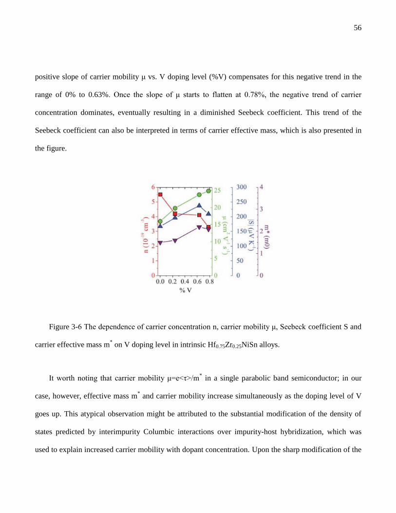
56
positive slope of carrier mobility μ vs. V doping level (%V) compensates for this negative trend in the
range of 0% to 0.63%. Once the slope of μ starts to flatten at 0.78%, the negative trend of carrier
concentration dominates, eventually resulting in a diminished Seebeck coefficient. This trend of the
Seebeck coefficient can also be interpreted in terms of carrier effective mass, which is also presented in
the figure.
Figure 3-6 The dependence of carrier concentration n, carrier mobility μ, Seebeck coefficient S and
carrier effective mass m* on V doping level in intrinsic Hf0.75Zr0.25NiSn alloys.
It worth noting that carrier mobility μ=e<τ>/m* in a single parabolic band semiconductor; in our
case, however, effective mass m* and carrier mobility increase simultaneously as the doping level of V
goes up. This atypical observation might be attributed to the substantial modification of the density of
states predicted by interimpurity Columbic interactions over impurity-host hybridization, which was
used to explain increased carrier mobility with dopant concentration. Upon the sharp modification of the
57
band structure, the calculated effective mass based on the simple parabolic band model thus appears
questionable. In light of this development, heat capacity measurements were performed to provide a
direction view of density of states increase at Fermi level.
Heat capacity measurements were performed on V-doped Hf0.75Zr0.25NiSn alloys. At temperatures
far below Debye temperature and Fermi temperature, the heat capacity of a solid can be expressed as a
combination of electrical and phonon contributions:
(3-4)
The electrical contribution is proportional to temperature T, while the phonon contribution is
proportional to T3. The Sommerfeld constant γ is used to derive the density of states at the Fermi level
N(EF) via the formula as:
( ) (3-5)
With the intercept of Cp/T vs. T plots being determined, N(EF) can then be figured out.
The Cp/T dependence on T2 is shown in Figure 3-7, and corresponding density of states at the Fermi
level at absolute zero temperature for different doping levels are listed in Table 1. A 23% increase in
density of states at the Fermi level was observed when vanadium’s doping level increased from 0% to
0.63%,. The Debye term of the heat capacity, given by the slope β, has almost no variation, which

58
indicates that there is little change in the phonon spectrum due to the introduction of impurity vanadium
atoms.
Figure 3-7 The dependence of heat capacity Cp on temperature at temperatures ranging from 1.8K
to 5.0K in V doped Hf0.75Zr0.25NiSn alloys, the inset shows that dependence of the Seebeck coefficient at
room temperature and density of state at the Fermi level on V doping level.
3-2-4 Conclusions of resonant states
Enhancement of the Seebeck coefficient was observed for V-doped intrinsic semiconductor
Hf0.75Zr0.25NiSn in the temperature range from 300K to 600K. The enhancement was attributed to the
localized density of states at Fermi level due to the resonance of introduced Vanadium’s d-orbitals with
matrix’s conduction band edge. This conclusion was analyzed in a single-band model via effective mass

59
calculation and then qualitatively explained using the Mott expression. Finally, low-temperature heat
capacity measurement was utilized to experimentally verify the existence of DOS increase near the
Fermi level.
3-3 Nanostructuring
Nanostructuring refers to various techniques used to construct nanostructured features in
conventional materials. Enhancement of thermoelectric properties can be achieved in nanostructured
form in means which are otherwise not possible in corresponding bulk form.[12], [67], [68] Hick and
Dresselhaus[69] were the first to propose to use lower dimensional structures to selectively modify
materials’ properties; they showed in their work that, by utilizing zero-, one- and two- dimensional
structures, one could obtain remarkable improvement in electronic properties. Theoretical work also
showed significant reductions in lattice thermal conductivity via nanostructuring in lower dimensional
nanostructures,[70] which was soon experimentally proved.[71], [72], [73], [74] Later on, a very low
thermal conductivity was reported in a three dimensional nanocomposite - ErAs nanoparticles embedded
In0.53Ga0.47As,[75] and enhanced Seebeck coefficients were also achieved in three dimensional
nanostructures.[76], [77]
Due to the relatively complex fabrication process and extremely low yield, lower dimensional
thermoelectric nanostructures are less favored to be applied in TE devices than their three dimensional
60
counterparts. Mechanical alloying (MA), melt spinning (MS), hydrothermal method and other methods
are employed to obtain three dimensional nanostructured thermoelectric materials. In our case, the MA
method, or also called ball milling (BM) was adopted.
3-3-1 Exploration in finding proper BM vessel
Mechanical alloying (MA) is a solid-state powder processing technique involving repeated cold
welding, fracturing, and re-welding of powder particles in a high-energy ball mill. It was originally
developed to produce oxide-dispersion strengthened (ODS) nickel- and iron- based super alloys for
applications in the aerospace industry. MA has now been shown to be capable of synthesizing a variety
of equilibrium and non-equilibrium alloy phases starting from blended elemental or pre-alloyed powders.
Mechanical alloying is akin to metal powder processing, where metals may be mixed to produce super
alloys. Mechanical alloying normally occurs in three steps. First, materials are alloyed in a ball mill and
ground to a fine powder. A hot pressing (HP) or Spark Plasma Sintering (SPS) process is then applied to
simultaneously compress and sinter the powder. A final heat treatment stage helps to remove residual
stresses produced during any cold compaction that may have been used.
Oxidizations, incomplete alloying, and contamination from BM vessels always cause remarkable
differences in thermoelectric properties, which are usually detrimental to figure of merit ZT; therefore,
well-selected BM vessels, reasonable BM time and an inert BM environment are key components
needed to obtain clean, fine and well-alloyed nanopowders.

61
Our first trial uses a hardened steel grinding vial set from SpexSamplePrep. The cylindrical vial is
2.25” in diameter and 3” in height (5.7 cm x 7.62 cm), with a volume of 65 mL. It also includes a screw-
on cap and two 0.5” (12.7 mm) and four 0.25” (6.35 mm) steel balls, these grinding balls as well as the
vessel are made of type 52-100 steel. Unfortunately, Fe contaminations were detected after five hours
BM, and the condition was even worsened with longer BM times. Our earlier research[44] found that
even a tiny bit of Fe content can lead to a fatal detriment to thermopower S. The reason is that Fe atoms
exist as P-type dopants upon replacing Ni atoms, while Zr(Hf)NiSn itself is an N-type semiconductor;
therefore, the Seebeck coefficient is harmed by the contradictory effect.
The next trial uses the 45 mL zirconia ceramic grinding vial set. The vial is 2.5” in diameter and
2.69”in height (6.35 cm by 6.8 cm). This zirconia set also includes a slip-on cap, and two zirconia balls
of 0.5” (12.7 mm) and the other two of 0.25” (6.4 mm). Although the hardness of ZrO2 is high (Mohs
8.5), contamination was still detected after only 5 hours of BM. The zirconia (ZrO2) impurity into HH
content resulted in significantly reduced electrical conductivity.
The most satisfactory vial set is made of 440C hardened stainless steel. This is a high-carbon high-
chromium stainless steel, capable of developing high hardness and high mechanical properties by
conventional heat treating methods. The 440C steel exhibits remarkable corrosion resistance in the
hardened condition. It has excellent resistance to wear and abrasion and is magnetic in all conditions. It
develops the highest hardness of the stainless steels. No obvious coarsened surface was found either on
the inner wall or on the grinding balls of this 440C stainless steel set, nor was contamination in intended
Half Heusler powders detected, even after 15 hours of continuous BM.

62
X-ray patterns in Figure 3-8 provide the evidences of contaminations when N-type
Hf0.6Zr0.4NiSn0.995Sb0.005 were ball milled in normal hardened steel vial set and in ZrO2 vial set. FeSn2
and ZrO2 contaminations were found in obtained nanopowders respectively.
Figure 3-8 X-Ray Diffraction patterns of as-cast Half Heusler Hf0.6Zr0.4NiSn0.995Sb0.005 (black) and
corresponding powders that were ball milled in normal iron vial set (blue) and that in ZrO2 vial set (red)
respectively.
3-4 Efforts on thermopower improvement via energy filtering

63
Low energy charge carriers are believed to be detrimental to the Seebeck coefficient S, thus S
could be enhanced if these low energy carriers can be selectively scattered. This concept of S
enhancement based on elimination of lower energy charge carriers can be expressed explicitly as:[5]
∫
( )(
( )
) (3-6)
Where e is the charge of an electron, ε is the energy of a carrier, μ is the chemical potential, σ(ε) is
the differential electrical conductivity and f0(ε) the Fermi distribution function. Moyzhes and
Nemchinsky[78] suggested that the contribution to thermopower from a carrier whose energy is lower
than its chemical potential is opposite to that of a carrier whose energy is higher than the chemical
potential; thus, the overall thermopower is reduced due to the contrary contribution. Therefore, if
transport of low energy carriers can be selectively eliminated by potential barriers, then thermopower S
(and hence the dimensionless figure of merit ZT) can be greatly improved. Next, we will estimate the
optimal barrier height in order to maximize figure of merit Z.
Considering degenerate semiconductors, the electronic part of figure of merit Z can be expressed as:
(3-7)
Where L0 (~2 WΩK-2
) is the Lorentz number. The electrical conductivity can be written as:
∫ ( )( ( )
) (3-8)

64
Now, considering a virtual change of differential electrical conductivity due to potential barrier
σ(ε) σ(ε)+ σ(ε), the change of figure of merit Z will then be:[79]
( ( ) ( )) ( ( )) ∫
( )
(3-9)
Thus the derivative of Z over σ(ε):
(
)(
( )
) (3-10)
Combining Eqn (3-9) with Eqn (3-10), the relative change in the figure of merit is then:
∫ (
) (
( )
)
( ) (3-11)
As shown in Figure 3-9, in a classic regime, carriers of energies lower than the potential barrier εb
are impeded by the barrier, while carriers whose energies are higher than εb would penetrate the
potential barrier unaffected; in other words, electrical conductivity in this classic regime is:
( ) { ( )
(3-12)

65
Figure 3-9 The preferential scattering mechanism of charge carriers in conduction band through
grain boundary of barrier height εb.
If we substitute σ(ε) of Eqn (3-12) into Eqn (3-11), we will find:
∫ (
) (
( )
)
( ) (3-13)
Only charge carriers with energy ε satisfying:
(3-14)
66
will bring a positive change in figure of merit; hence, in order to maximize Z, Eqn (3-14) shall hold
true for all ε<εb; this requirement can always be satisfied only if:
(3-15)
It can be seen from this equation that the elimination of lower energy charge carriers by the
appropriate potential barrier will always lead to enhancement in Z as long as εb>0.
More rigorous treatments on the effect of potential barriers on electrical transport and thermal
transport have been well discussed. Impressive enhancement in the power factor[19], [78], [80], [81],
[82], together with reduced thermal conductivity,[83] were achieved, resulting in a very promising
figure of merit applicable in building TE generators and coolers.
Although precise control of the height and width of potential barriers may be achieved via lower
dimensional nanostructuring, due to the relatively complex technique and extremely low yields,
researches are mostly focused on three-dimensional nanocomposites.
3-4-1 Monolithic N-type HH nanocomposite
To prepare N-type Half Heusler Hf0.6Zr0.4NiSn0.995Sb0.005, high purity (>99.95%) Hf, Zr, Ni, Sn and
Sb elemental pieces were arc melted three times under an argon atmosphere to ensure homogeneity. The
obtained ingot was then pulverized using mortar and pestle before being moved to a BM vessel for 15
hours’ mechanical alloying. The BM process was conducted under a protecting atmosphere of argon.
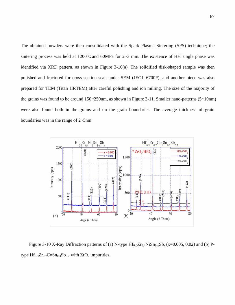
67
The obtained powders were then consolidated with the Spark Plasma Sintering (SPS) technique; the
sintering process was held at 1200 and 60MPa for 2~3 min. The existence of HH single phase was
identified via XRD pattern, as shown in Figure 3-10(a). The solidified disk-shaped sample was then
polished and fractured for cross section scan under SEM (JEOL 6700F), and another piece was also
prepared for TEM (Titan HRTEM) after careful polishing and ion milling. The size of the majority of
the grains was found to be around 150~250nm, as shown in Figure 3-11. Smaller nano-patterns (5~10nm)
were also found both in the grains and on the grain boundaries. The average thickness of grain
boundaries was in the range of 2~5nm.
Figure 3-10 X-Ray Diffraction patterns of (a) N-type Hf0.6Zr0.4NiSn1-xSbx (x=0.005, 0.02) and (b) P-
type Hf0.3Zr0.7CoSn0.3Sb0.7 with ZrO2 impurities.
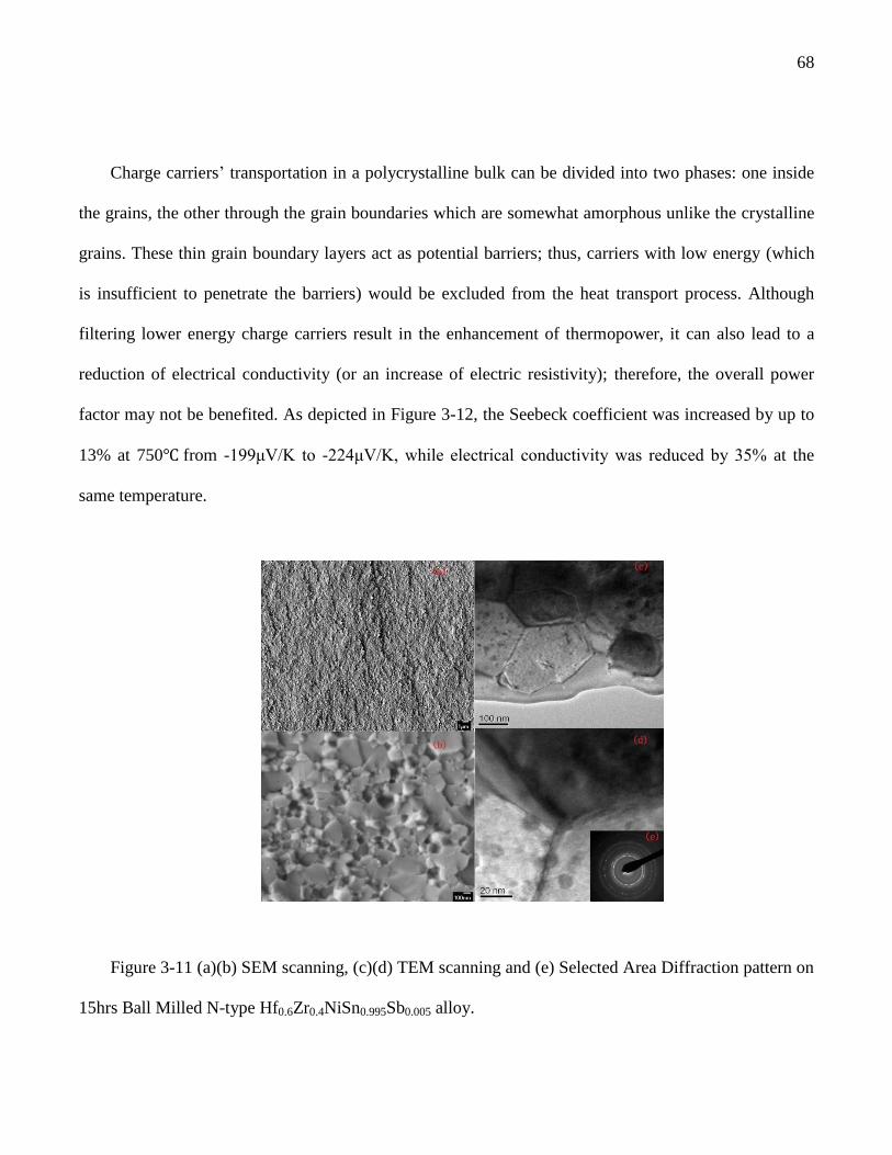
68
Charge carriers’ transportation in a polycrystalline bulk can be divided into two phases: one inside
the grains, the other through the grain boundaries which are somewhat amorphous unlike the crystalline
grains. These thin grain boundary layers act as potential barriers; thus, carriers with low energy (which
is insufficient to penetrate the barriers) would be excluded from the heat transport process. Although
filtering lower energy charge carriers result in the enhancement of thermopower, it can also lead to a
reduction of electrical conductivity (or an increase of electric resistivity); therefore, the overall power
factor may not be benefited. As depicted in Figure 3-12, the Seebeck coefficient was increased by up to
13% at 750 from -199μV/K to -224μV/K, while electrical conductivity was reduced by 35% at the
same temperature.
Figure 3-11 (a)(b) SEM scanning, (c)(d) TEM scanning and (e) Selected Area Diffraction pattern on
15hrs Ball Milled N-type Hf0.6Zr0.4NiSn0.995Sb0.005 alloy.

69
Without considering the reduction in thermal conductivity, an overall 15% reduction in Power
Factor S2T/ρ was obtained as shown in Figure 3-13, mainly due to the significantly reduced carrier
concentration by potential barrier scattering. A simple model can be utilized to demonstrate the
reduction of total electrical conductivity across potential barriers (grain boundaries):[81]
(3-16)
Where “total” represents the overall carrier transportation, “grain” represents carrier transportation
inside grains, and “gb” represents transportation through grain boundaries. L is the length scale. Within
classical regime, low energy charge carriers (ε < barrier height εb) will be confined within grains and
thus do not contribute to electrical conductivity. In the case of σgb(ε)=σgrain(ε) for ε >= εb, and
Lgrain+Lgb=Ltotal, from Eqn (3-16):
∫ ( ) ( ) ∫ ( ) ( ) ∫ ( ) ( )
(3-17)
This simplified calculation reveals the fact that the overall electrical conductivity is always reduced
as long as low energy carriers are filtered by potential barriers.

70
Figure 3-12 Measured electrical resistivity (Ohm*m) and thermopower S (V/K) of N-type Half
Heusler Hf0.6Zr0.4NiSn0.995Sb0.005 which was SPSed at 1000 after 15 hours BM (red square), compared
with the properties of its bulk counterpart (black square).
Figure 3-13 Power factor S2T/ρ dependent on temperature in monolithic nanostructured
Hf0.6Zr0.4NiSn0.995Sb0.005.
71
Neophytou et al.[81] have made use of similar treatment in Si nanowires system and suggested
that the reduction of electrical conductivity due to barrier potential scattering would not diminish until
the Fermi level was increased high enough for the carriers to be thermionically emitted over the
potential barriers, and enhanced Fermi level can be achieved via heavier doping. Although increasing
the doping level normally leads to a reduction in thermopower S, the combined effect of energy filtering
and increased carrier concentration would still get to an optimal point where the overall power factor
(PF=S2σT) can be enhanced. In the N-type HH system, increasing the Sb doping level from 0.5% to
1%~2%, while keeping grain size and grain boundary thickness constant, may be an effective means to
achieve overall enhancement of the Power Factor. Too high a doping level will not result in further
enhancement of the TE properties. On one hand, increasing the doping level eventually leads to enlarged
bipolar effect detrimental to thermopower S; on the other hand, according to the Wiedemann-Franz law,
electrical thermal conductivity κe=L0σT would increase as σ goes up, resulting in an overall higher
thermal conductivity.
Beside the dependence of thermoelectric properties on barrier height, the dependence of
thermopower on the density of potential barriers was also discussed by Nishio and Hirano.[79]
3-4-2 Nanoparticles embedded in P-type bulk HH
In addition to monolithic nanostructures, nanocomposites constructed by implementing
nanoparticles into bulk materials externally or nanocomposites with in-situ formed secondary phases are

72
also commonly used. The embedded nanoparticles not only serve as scattering centers of phonons and
charge carriers, but are also able to suppress the grain growth of matrix materials.
In this section, ZrO2 nanoparticles (grain size ~80nm) dispersed P-type HH Hf0.3Zr0.7CoSn0.3Sb0.7
nanocomposites were synthesized. First, bulk ingots of Hf0.3Zr0.7CoSn0.3Sb0.7 were fabricated from
elemental pieces in an argon atmosphere using the arc melting technique; the obtained ingots were then
pulverized and hand ground to micron size with mortar and pestle. Next, commercially available high
purity ZrO2 nanopowders were added into micron-sized HH powders and hand ground for 10 minutes to
allow for homogeneous mixing; another 15 minutes of BM was also applied to further disperse these
ZrO2 nanopowders into matrix materials. The mixed powders were eventually consolidated with Spark
Plasma Sintering, with sintering temperature of 1200 and pressure of 60MPa.
The existence of the oxide phase was identified via XRD peaks shown in Figure 3-10b. Scanning
electron microscope (SEM, JEOL 6700F) and transmission electron microscope (TEM, JEOL 2000FX)
were also employed to study their morphologies and microstructures. Energy dispersive spectroscopy
(EDS) line scan further confirmed the existence of the oxide particles as well the homogeneity of
samples.
In Figure 3-10(b), the existence of an impurity oxide phase can be identified, however, the exact
composite is still pending, due to the similar crystal structure and lattice constant of HfO2 and ZrO2; thus,
further scanning under TEM and SEM is necessary.

73
Figure 3-14 (a) Microstructure of P-type HH Hf0.3Zr0.7CoSn0.3Sb0.7 under TEM, and selected area
diffraction as well as corresponding EDS at (b) nanoparticle B (c) matrix area E.
Presented in Figure 3-14(a) are TEM images of Hf0.3Zr0.7CoSn0.3Sb0.7 bulk which was dispersed
with 2 vol.% ZrO2 nanoparticles. Nanograins of 50 to 80 nm in size can be found at the boundaries of
HH grains, meanwhile, nanoparticles as large as 200-300 nm in size were also detected. Select area
diffraction patterns as well as energy dispersive spectroscopy at spots B (nanoparticle) and E (main
matrix), as shown in Figures 3-14(b) and 3-14(c), further confirmed that these nanoparticles were indeed
oxides and they had different crystal structures than the matrix.
The morphological structure of the same nanocomposite were studied under SEM and shown in
Figures 3-15(a) and 3-15(b). The typical grain size of host material was in the range of 5-25μm, while
that of nanoinclusions fell between 80 and 250 nm. The ZrO2 coagulations (~250nm) were probably due

74
to insufficient mixing during BM. The EDS patterns shown in Figure 3-15(c) indicate that the
composition of the nanoinclusions is mainly HfO2, since the contents of Hf and O always peak
synchronously whenever the line scan crosses a nanoparticle.
Figure 3-15 (a)(b) SEM scanning of fractured P-type HH Hf0.3Zr0.7CoSn0.3Sb0.7, and (c) energy
dispersive spectroscopy line scan along the path shown in (b).
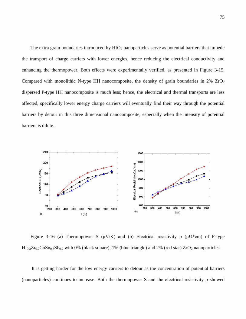
75
The extra grain boundaries introduced by HfO2 nanoparticles serve as potential barriers that impede
the transport of charge carriers with lower energies, hence reducing the electrical conductivity and
enhancing the thermopower. Both effects were experimentally verified, as presented in Figure 3-15.
Compared with monolithic N-type HH nanocomposite, the density of grain boundaries in 2% ZrO2
dispersed P-type HH nanocomposite is much less; hence, the electrical and thermal transports are less
affected, specifically lower energy charge carriers will eventually find their way through the potential
barriers by detour in this three dimensional nanocomposite, especially when the intensity of potential
barriers is dilute.
Figure 3-16 (a) Thermopower S (μV/K) and (b) Electrical resistivity ρ (μΩ*cm) of P-type
Hf0.3Zr0.7CoSn0.3Sb0.7 with 0% (black square), 1% (blue triangle) and 2% (red star) ZrO2 nanoparticles.
It is getting harder for the low energy carriers to detour as the concentration of potential barriers
(nanoparticles) continues to increase. Both the thermopower S and the electrical resistivity ρ showed
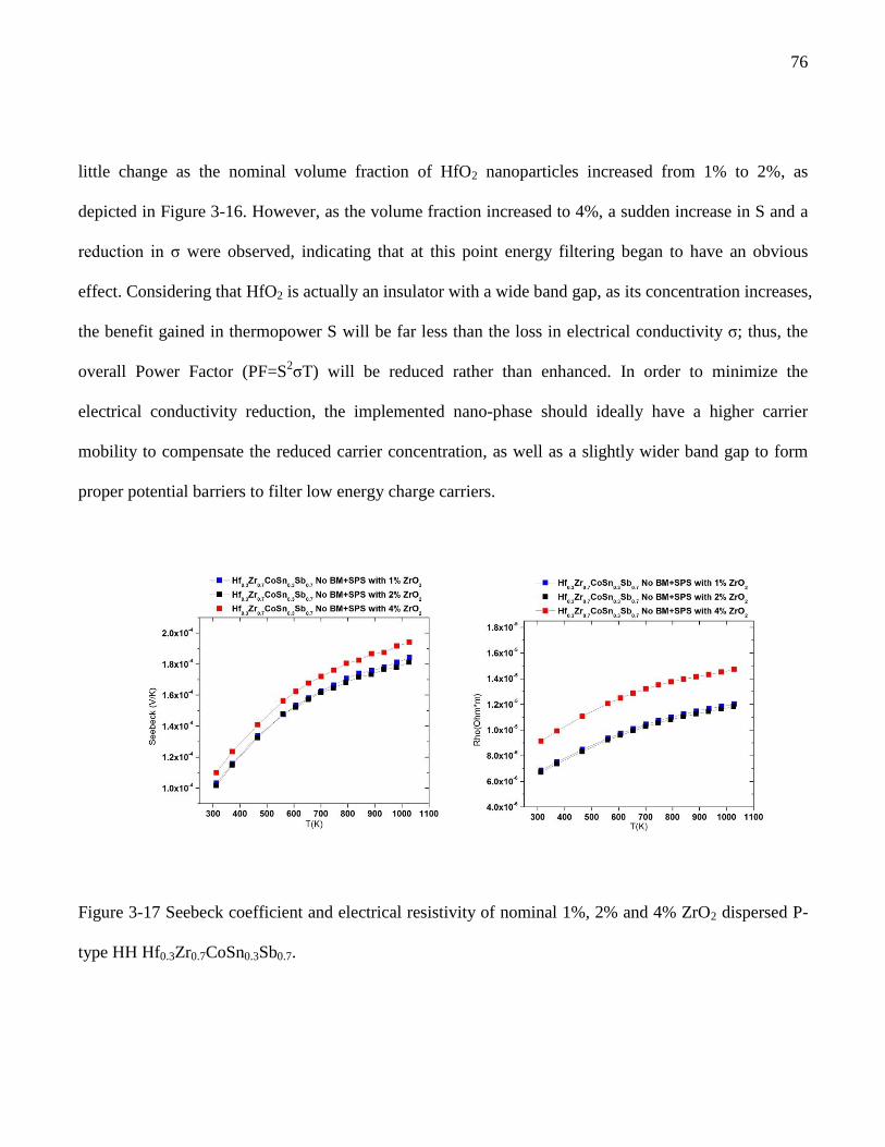
76
little change as the nominal volume fraction of HfO2 nanoparticles increased from 1% to 2%, as
depicted in Figure 3-16. However, as the volume fraction increased to 4%, a sudden increase in S and a
reduction in σ were observed, indicating that at this point energy filtering began to have an obvious
effect. Considering that HfO2 is actually an insulator with a wide band gap, as its concentration increases,
the benefit gained in thermopower S will be far less than the loss in electrical conductivity σ; thus, the
overall Power Factor (PF=S2σT) will be reduced rather than enhanced. In order to minimize the
electrical conductivity reduction, the implemented nano-phase should ideally have a higher carrier
mobility to compensate the reduced carrier concentration, as well as a slightly wider band gap to form
proper potential barriers to filter low energy charge carriers.
Figure 3-17 Seebeck coefficient and electrical resistivity of nominal 1%, 2% and 4% ZrO2 dispersed P-
type HH Hf0.3Zr0.7CoSn0.3Sb0.7.

77
3-5 Reduction of thermal conductivity
The introduction of nano-scale features not only affects the charge carriers’ transport, resulting in
changes in thermopower and electrical conductivity, but also provides extra phonon scattering centers,
leading to a reduction in the lattice thermal conductivity. According to Callaway[57] and Peacor et
al.[84], lattice thermal conductivity can be expressed as:
(
) ∫
( )
⁄
(3-18)
Where x is the reduced phonon frequency x=ħω/kBT, and τph is the relaxation time, which consists
of three components and can be expressed with Matthiessen’s rule:
⁄ ⁄ (3-19)
τI-1
(~ω4) represents impurity scattering due to mass fluctuation (density/strain), the second term τU
-1
(~ω2) is Umklapp scattering involving multiple-phonon interactions, and the last term (~ω
0) stands for
phonon’s grain boundary scattering with group velocity vs and grain size d. Parameter A and parameter
B are constant for a certain composite. For a polycrystalline bulk sample with grain size ~10-5
m, the
third term is estimated to be 103m/s/10
-5m=10
8s
-1, it can be seen that grain boundary scattering term is
almost constant at all temperatures. At temperatures far below the Debye temperature, boundary
scattering and impurity scattering dominate, while the temperature is around or above Debye
temperature, the grain boundary scattering no longer plays that important a role in obstructing phonon
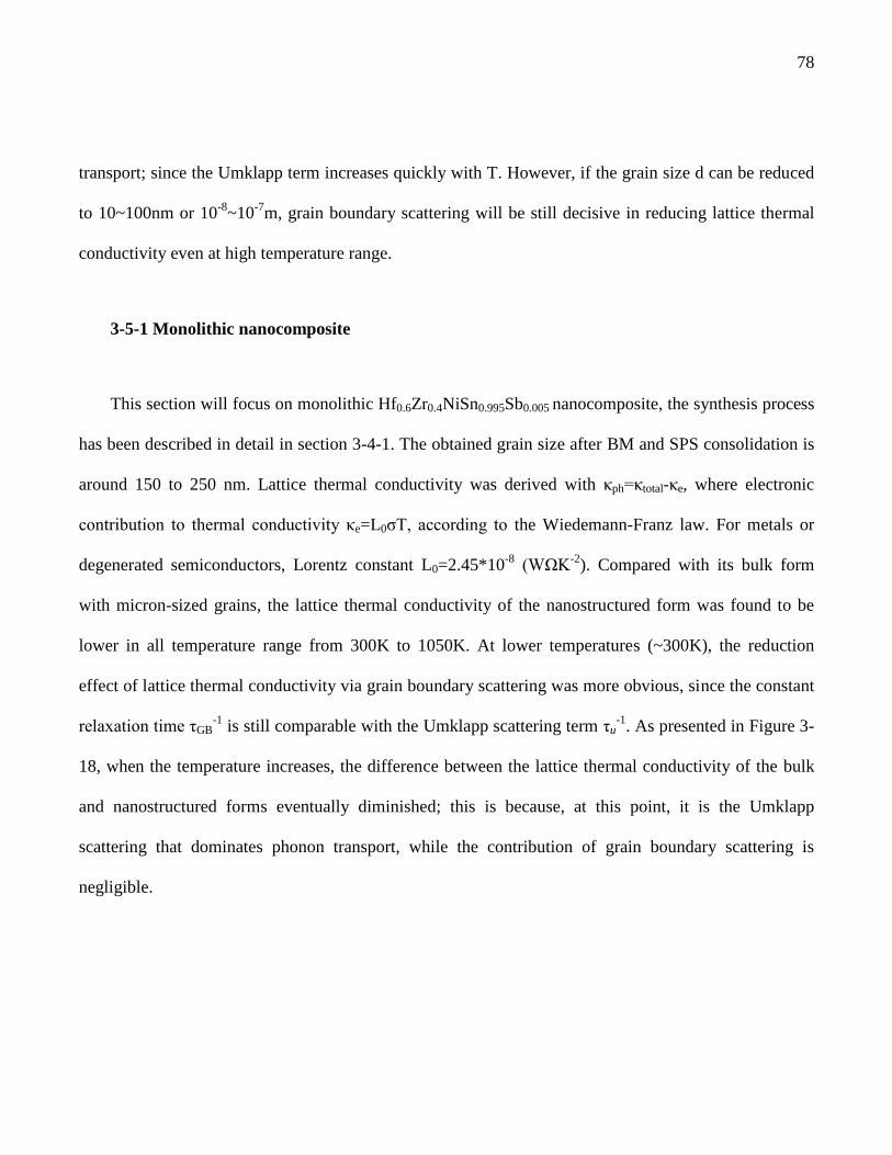
78
transport; since the Umklapp term increases quickly with T. However, if the grain size d can be reduced
to 10~100nm or 10-8
~10-7
m, grain boundary scattering will be still decisive in reducing lattice thermal
conductivity even at high temperature range.
3-5-1 Monolithic nanocomposite
This section will focus on monolithic Hf0.6Zr0.4NiSn0.995Sb0.005 nanocomposite, the synthesis process
has been described in detail in section 3-4-1. The obtained grain size after BM and SPS consolidation is
around 150 to 250 nm. Lattice thermal conductivity was derived with κph=κtotal-κe, where electronic
contribution to thermal conductivity κe=L0σT, according to the Wiedemann-Franz law. For metals or
degenerated semiconductors, Lorentz constant L0=2.45*10-8
(WΩK-2
). Compared with its bulk form
with micron-sized grains, the lattice thermal conductivity of the nanostructured form was found to be
lower in all temperature range from 300K to 1050K. At lower temperatures (~300K), the reduction
effect of lattice thermal conductivity via grain boundary scattering was more obvious, since the constant
relaxation time τGB-1
is still comparable with the Umklapp scattering term τu-1
. As presented in Figure 3-
18, when the temperature increases, the difference between the lattice thermal conductivity of the bulk
and nanostructured forms eventually diminished; this is because, at this point, it is the Umklapp
scattering that dominates phonon transport, while the contribution of grain boundary scattering is
negligible.
79
Figure 3-18 (a)Total thermal conductivity (solid lines) and lattice thermal conductivity (solid
squares) (b) figure of merit ZT of N-type HH Hf0.6Zr0.4NiSn0.995Sb0.005 with 0hr (black), 10hrs (blue) and
15hrs (red) Ball Milling time.
3-5-2 Nanoparticles embedded in bulk
ZrO2 nanoparticles of 1%, 2% and 4% nominal volume fractions were dispersed into P-type HH
Hf0.3Zr0.7CoSn0.3Sb0.7 bulk, as described in section 3-4-2. It was found, as shown in Figure 3-15(b) and
Figure 3-14(a), that most of the HfO2 (due to Zr-Hf exchange with host material) nanoparticles (~80nm)
lay at matrix grain boundaries. No obvious reduction in lattice thermal conductivity was observed upon
ZrO2 nanoparticle dispersion, except for the nominal 2% ZrO2 dispersed nanocomposite. According to
the experimental results,[85], [86] even a small volume percentage of nanoparticles would cause a
considerable reduction in lattice thermal conductivity. In our case, as shown in Figure 3-19, the

80
unconspicuous change in lattice thermal conductivity is either because the embedded HfO2 nanoparticles
have aggregated into larger micron-sized precipitates or because the nanopowders were not thoroughly
dispersed into matrix; in either event, the role of added nanoparticles as phonon scattering centers was
weakened.
Figure 3-19 Lattice thermal conductivity of P-type HH Hf0.3Zr0.7CoSn0.3Sb0.7 bulk (grey) and
corresponding nanocomposistes with 1% (blue), 2% (black) and 4% (red) ZrO2 nanoparticles.
Although further increase of ZrO2 content might result in lower lattice thermal conductivity, it is
nevertheless the case, as discussed in section 3-4-2, that too large a ZrO2 volume fraction would lead to
an extremely high electrical resistivity, which is unlikely to be compensated by the possible
enhancement gained by thermopower and reduction grained in thermal conductivity. Actually, 2% ZrO2

81
was found to be the optimal volume fraction, which eventually leads to an overall improvement in figure
of merit ZT, as can be seen in Figure 3-20.
Figure 3-20 The dependence of figure of merit ZT on temperature in 1%, 2% and 4% ZrO2
dispersed Hf0.3Zr0.7CoSn0.3Sb0.7.
3-6 Mass Fluctuation Effect on Lattice Thermal Conductivity
To analyze the mass fluctuation effect, one should recall the impurity scattering term of relaxation
time as expressed in Eqn (3-19), τI-1
=Aω4. According to Callaway[57] and Klemens,[87] the
composition dependent constant A can be expressed as:

82
∑ ( )
(3-20)
Where V0 is the volume per atom, Mi is the mass of atom i, fi is the fraction of atoms with mass Mi,
and M is the average atom mass. This effective medium approach, was also adopted by Mingo et al.[88]
to evaluate parameter A in a two-phase heterogeneous system, in which case, A is expressed as:
( )
(3-21)
Regardless of the expression of A, a maximal τI-1
=Aω4
shall be achieved at certain ratio of
constituents, this maximum of τI-1
corresponds to the lowest lattice thermal conductivity that can be
obtained solely by mass fluctuation.
In N-type Half Heusler Hf0.6Zr0.4NiSn0.995Sb0.005, Hf atoms can be replaced by Zr or Ti atoms within
the same group in periodic table. The mass difference between Hf and Ti is the largest, therefore, the
mass fluctuation parameter A shall be increased if some heaviest Hf atoms are to be replaced by the
lightest Ti atoms, in this way, a reduced lattice thermal conductivity can be expected. Experiments have
been performed on Hf0.6Zr0.4NiSn0.995Sb0.005; upon 10% and 20% Hf being replaced by Ti atoms, the
lattice thermal conductivity was reduced consistently at all temperatures ranging from 300K to 1050K.
The different behaviors between lattice thermal conductivity reduction caused by grain boundary
scattering as shown in Figure 3-18 and that caused by mass fluctuation as shown in Figure 3-21 can be
ascribed to their different frequency dependences; while τGB-1
stays constant as temperature increases,τI-1
increases with the fourth power of phonon frequency ω. At high temperatures, most phonons are

83
populated close to the Brillouin zone boundary (the high frequency region), thus, the contribution of
mass fluctuation τI-1
increases; while the contribution of grain boundary scattering τGB-1
stays constant.
Considering the dominating Umklamp scattering is increasing as temperature goes up, the relative
contribution of mass fluctuation to phonon scattering may stay unchanged, while the relative
contribution of grain boundary scattering will significantly decrease. Although a lower lattice thermal
conductivity has been achieved upon replacing a certain percentage of Hf atoms with lighter Ti atoms,
severe degradation in thermopower results in an reduction in power factor, eventually leading to an
overall lower dimensionless figure of merit ZT at high Ti doping levels. It was found that only when 10%
Hf atoms were replaced by Ti atoms, was a higher overall ZT observed, as shown in Figure 3-22.
Figure 3-21 Lattice thermal conductivity and power factor of nanostructured Hf0.6Zr0.4NiSn0.995Sb0.005
with 0% (black), 10% (white), and 20% (blue) Hf atoms replaced by smaller Ti atoms.
84
3-7 Conclusions
Vanadium doped Half Heusler Hf0.75Zr0.25NiSn alloys were fabricated with the arc melting
technique. Enhancement of the Seebeck coefficients were observed from 300K to 600K, which was
explained by the localized increase of Density of States (DOS) at the Fermi level due to the state
resonance of impurity orbits and matrix band edges. Evidence of the density of states increase at the
Fermi level EF was eventually exhibited by low temperature specific heat measurements.
Nanostructured N-type Hf0.6Zr0.4NiSn0.995Sb0.005 and P-type Hf0.3Zr0.7CoSn0.3Sb0.7 Half Heusler
alloys were synthesized with arc melting, mechanic alloying and SPS consolidation. While N-type
Hf0.6Zr0.4NiSn0.995Sb0.005 was a monolithic nanostructure with grain size around 150 to 250 nm, P-type
Hf0.3Zr0.7CoSn0.3Sb0.7 bulk was implemented with inert ZrO2 nanoparticles, which mostly stayed at
matrix grain boundaries and evidenced by EDS line scan and SEM. A remarkable increase in the density
of grain boundaries was generated upon introducing these nanostructured features. The effect of low
energy charge carriers being selectively scattered by additional grain boundaries on thermopower S and
electrical conductivity σ was then discussed in both monolithic N-type and ZrO2 dispersed P-type
nanostructured Half Heusler alloys. The increased density of grain boundaries in nanostructured alloys
also prompted a significant decrease in lattice thermal conductivity due to the additional phonon grain
boundary scattering. A phenomenological effective medium method will be introduced to quantitatively
calculate the reduction in lattice thermal conductivity of various nanostructures in Chapter 5.

85
Finally, the mass fluctuation effect was applied to further reduce the lattice thermal conductivity.
The mechanism was discussed using the Callaway model. A consistently lower lattice thermal
conductivity was observed in N-type Hf0.6Zr0.4NiSn0.995Sb0.005 upon 10% and 20% Hf atoms being
replaced by lighter Ti atoms.
Overall, the highest dimensionless figure of merit of ZT=1.0 for N-type HH was achieved at 850K
in monolithic nanocomposite Ti0.1Hf0.5Zr0.4NiSn0.995Sb0.005 as the result of combining nanostructuring
and mass fluctuation, while ZT=0.85 for P-type HH was achieved at 1050K in 2% ZrO2 dispersed
Hf0.3Zr0.7CoSn0.3Sb0.7 solely via nanostructuring technique, as shown in Figure 3-22.
Figure 3-22 Figure of merit ZT achieved of Half Heusler alloys (a) N-type: ZT=1.0 at 850K in
monolithic Ti0.1Hf0.5Zr0.4NiSn0.995Sb0.005 (b) P-type: ZT=0.85 at 1050K in 2% ZrO2 nanoparticles
dispersed Hf0.3Zr0.7CoSn0.3Sb0.7.

86
4. Nanostuctured silicon germanide as prospective thermoelectrics
Silicon germanide (Si1-xGex, x=0~1) is one of the most widely studied and applied thermoelectric
materials for power generation at high temperatures above 800 . It has been used in Radioisotope
Thermoelectric Generators (RTGs) powering NASA space crafts since 1976.[16] Besides thermoelectric
performance, SiGe alloys also have many merits including high mechanical strength, high melting point,
low vapor pressure, and excellent resistance to oxidization; therefore, they are of great interest for
industrial waste heat recovery, the auto industry and solar thermopower plants.
The milestone of dimensionless figure of merit ZT for n-type bulk Si1-xGex is P-doped Si80Ge20 with
ZT~1;[16] for p-type bulk, it is B-doped Si80Ge20 with ZT~0.5.[89] The obvious lower ZT of p-type
Si80Ge20 can be largely attributed to the comparably lower carrier mobility of holes than that of electrons
in its n-type analogue. It was not until recently, when nanostructuring techniques were introduced to
thermoelectrics fabrication, that significant higher ZTs were reported for SiGe with n-type ZT~1.3, p-
type~0.95 by the Boston College group.[17], [21] The improvement is primarily the result of dramatic
reduction in lattice thermal conductivity in nanostructured form due to the much more intense phonon
interface scattering than in bulk form. However, the fabrication processes have rarely been discussed in
detail, and, as we will present in this chapter, the TE properties are very sensitive to the consolidation
parameters (sintering temperature, pressure and holding time); thus, only an optimized synthesis process
will lead to the optimal figure of merit ZT, whereas a deviation in fabrication process might cause

87
severely degraded TE properties. Novel core-shell structures were also fabricated using the wet method
by collaborator Nanosonic Inc., and the dramatic reduction in lattice thermal conductivity was observed.
4-1 Synthesis of samples
A fine powder mixture of Silicon (100mesh), Gemernium (200mesh) and Phosphorous or Boron
(50mesh) of 5~10 grams was loaded into a 440C stainless steel vial, together with two 0.5” and four
0.25” 440C ultra hard stainless steel balls. The process was performed in a glove box at argon
atmosphere. The vial was then sealed and positioned in a SPEX 8000D vibrational mixer, which was
then seated in a sealed aluminum box filled with argon. The BM processes were paused for half an hour
every three hours to avoid overheating. Dodecane was also introduced to reduce the cold welding
between loaded powders and the vial’s inner wall. The obtained nanopowders were removed from the
grinding vials in the glove box after the BM process was complete. At this point, the powders should be
either stored for future use in an inert atmosphere to avoid oxidization or consolidated immediately with
Spark Plasma Sintering technique. SPS temperature and holding time were varied to study the
dependence of TE properties on condensing parameters, while sintering pressure was kept constant at
60MPa.

88
4-2 Grain size vs. BM time
To investigate the effect of BM time on obtained grain size, n-type Si80Ge20P2 nanopowders were
prepared under the same grinding conditions, using vibrational BM for both 5 hours and 15 hours
separately. The obtained nanopowders were then examined under TEM. The size of the nanoparticles
after five hours of ball milling varied from 30nm to 300nm, as shown in Figure 4-1(a). In Figure 4-1(b),
under a higher magnification it was found that the large nanoparticles were actually aggregates of finer
crystalline grains of 10nm~30nm. Figure 4-1(c) provides a better image of the fine grains composing the
larger aggregates. The inset is the selected area electron diffraction pattern (SAED) on a dark large grain,
which confirmed that the dark grains were aggregates of smaller multicrystalline grains. Nanoparticles,
after 15 hours of ball milling, showed little difference in grain size from those that were ball milled for
only 5 hours, as shown in Figure 4-2; similar aggregates of finer grains were also found.
The disability of extending ball milling time to further reduce grain size could be attributed to the
size of the grinding balls, which may have been comparably too large (0.5” x 2 + 0.25” x 4); or the high
energy vibration ball mill process is so effective that the pulverizing limit has been reached within 5
hours. Now that BM limit can be reached in 5 hours, to avoid possible contamination in a long term ball
milling process and to further reduce the grain size, 5 hours BM time and smaller grinding balls are thus
suggested in the future work.

89
Figure 4-1 TEM images of nanoscaled aggregates in Si80Ge20P2 nanopowders which were ball milled 15
hours.
Figure 4-2 TEM images of nanoscaled aggregates in Si80Ge20P2 nanopowders which were ball milled 15
hours.
4-3 Porosity vs. sintering temperature

90
To investigate the effect of sintering temperature on the microstructure of consolidated samples,
Si80Ge20P2 nanopowders that have been ball milled for 15 hours were then SPS compressed at 900 ,
1000 and 1100 , separately, with the same pressure (60MPa) and holding time. Mass densities were
measured using the Archimedes method and found to be 2.89 g/cc, 2.94g/cc and 3.03g/cc respectively.
In comparison with the theoretical density of 2.98g/cc, samples condensed at 900 and 1000 showed
somewhat porous features. The porosity is evidenced by the relatively high electrical resistivity, since
charge carriers tend to be significantly scattered by the introduced vacancies and thick grain boundaries
due to porosity, resulting in very low carrier conductivity. As presented in Figure 4-3(a), the electrical
resistivity of the sample condensed at 900 was almost doubled, while that of the sample SPS at
1000 was found to have increased only by 50%, compared with the fully condensed sample SPS at
1100 . The corresponding Seebeck coefficients, shown in Figure 4-3(b), also showed a systematic
increasing trend as condensation temperature increased from 900 to 1100 , indicating a decreased
porosity. As discussed in Chapter 3, low energy charge carriers are detrimental to thermopower, thus if
these carriers were strongly scattered by the vacancies and grain boundaries in a porous sample, the
overall thermopower was then enhanced. However, the benefit gained from the enhanced thermopower
S was not enough to compensate for the loss in electrical conductivity; in the end, power factor S2σ/T
was reduced due to porosity, as seen in Figure 4-3(c).

91
Figure 4-3 Electrical resistivity (a), Seebeck coefficient (b) and Power Factor (c) of Si80Ge20P2
sintered at 900 (black), 1000 (blue) and 1100 (red) separately.
4-4 Grain growth in SPS consolidation process
In this section, the grain growth during SPS is investigated. Nanopowders obtained from 5 hours
BM and 15 hours BM were consolidated with SPS, at the same heating rate of 200 /min, sintering
temperature of 1100 , pressure of 60MPa and holding time of 6 min. For convenience, the two
samples were named SGP-T1-05 and SGP-T1-15 respectively. The mass densities, measured using the
Archimedes method, were found to be 3.00 g/cc and 2.99 g/cc, respectively; both values were close to
the theoretical value of 2.98 g/cc, indicating full condensations. No impurity phases were found in either
sample, according to the XRD scanning, as shown in Figure 4-4, and the diffraction peaks were
somewhat shifted due to Si-Ge alloying, compared with these of a Si single crystal.

92
The average size D of crystalline grains in consolidated samples can be estimated with Scherrer’s
method as:[90]
(4-1)
Where K is the Scherrer constant, a shape factor which approximates 0.89 (ratio of full width at half
maximum (FWHM) and the integrated breath), λ is the incident wavelength of X-Ray (~0.154nm for
Cu-Kα source), w is the FWHM of a peak at 2θ, and θ is the incident angle with diffraction plane. The
average grain sizes of SGP-T1-05 and SGP-T1-15 were calculated to be 54.0 nm and 50.6 nm,
respectively. The small difference in grain size between disk sample ball milled for 5 hours and the one
for 15 hours was also reflected in their close lattice thermal conductivities, as shown in Figure 4-5.
Figure 4-4 XRD pattern of SGP-T1-05 and SGP-T1-15, the inset shows corresponding peaks at (111).

93
Significant grain growth was disclosed by comparing the grain size in consolidated samples with
that in corresponding nanopowders. According to Sherrer’s equantion, wider diffraction peaks
correspond to smaller crystalline grains, and vice versa; as the grain size increases, diffraction peaks
become sharper. XRD patterns of Si80Ge20P2 nanopowders (15 hours BM) and the consolidated
counterpart are presented in Figure 4-6. A significant grain growth during the consolidation process is
indicated by the remarkable reduction in corresponding peak’s width in condensed sample.
Figure 4-5 Lattice thermal conductivity of SGP-T1-05 and SGP-T1-15.
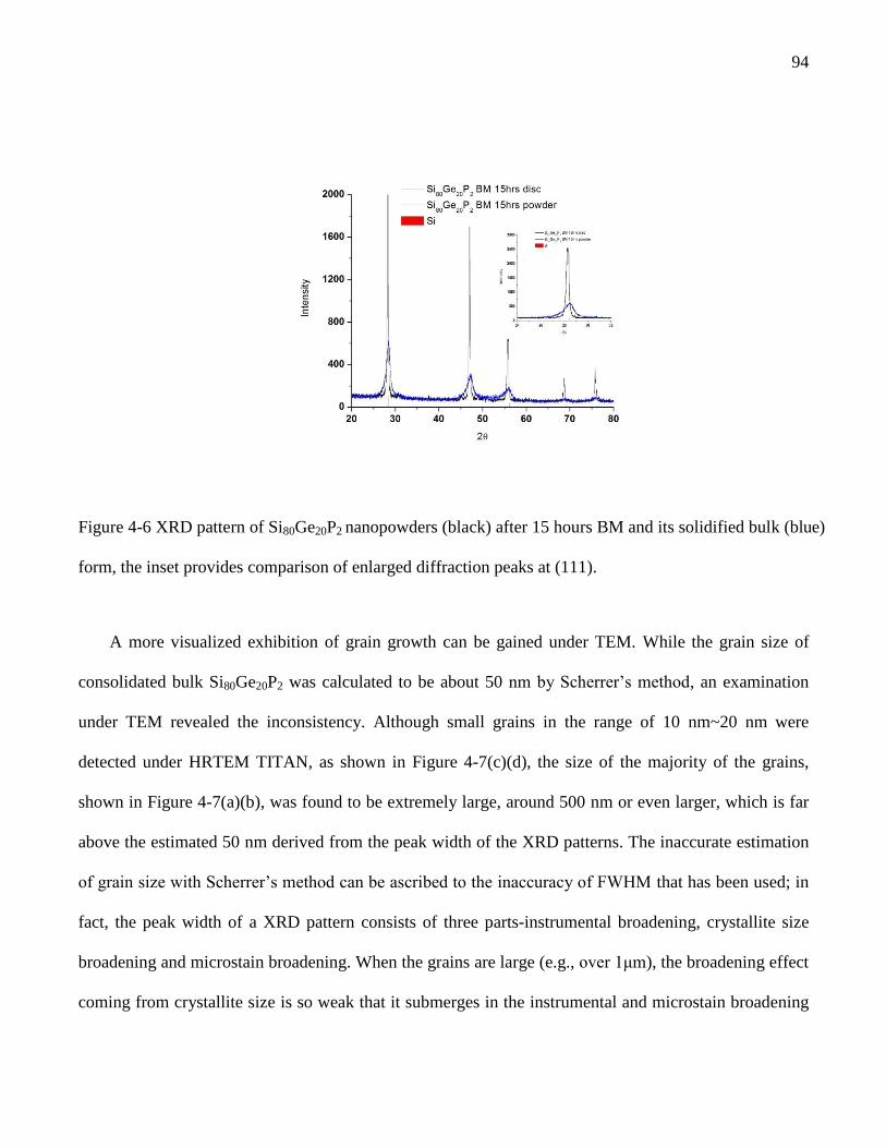
94
Figure 4-6 XRD pattern of Si80Ge20P2 nanopowders (black) after 15 hours BM and its solidified bulk (blue)
form, the inset provides comparison of enlarged diffraction peaks at (111).
A more visualized exhibition of grain growth can be gained under TEM. While the grain size of
consolidated bulk Si80Ge20P2 was calculated to be about 50 nm by Scherrer’s method, an examination
under TEM revealed the inconsistency. Although small grains in the range of 10 nm~20 nm were
detected under HRTEM TITAN, as shown in Figure 4-7(c)(d), the size of the majority of the grains,
shown in Figure 4-7(a)(b), was found to be extremely large, around 500 nm or even larger, which is far
above the estimated 50 nm derived from the peak width of the XRD patterns. The inaccurate estimation
of grain size with Scherrer’s method can be ascribed to the inaccuracy of FWHM that has been used; in
fact, the peak width of a XRD pattern consists of three parts-instrumental broadening, crystallite size
broadening and microstain broadening. When the grains are large (e.g., over 1μm), the broadening effect
coming from crystallite size is so weak that it submerges in the instrumental and microstain broadening

95
background; only when the grain size is no more than a few hundred nanometer can the peak width of
the XRD patterns be dominated by crystallite size broadening effect, in which case a reasonable
approximation of grain size from Scherrer’s method can be possibly made. Compared with the grain size
of Si80Ge20P2 nanopowders (10~30 nm under TEM as shown in Figure 4-2), remarkable grain growth
did take place during SPS process.
Figure 4-7 Grains of SPS consolidated Si80Ge20P2 with 5 hours BM time under JOEL 2000FX showing
the huge majority grains in (a)(b), and HRTEM Titan showing the existence of small minority grains in
(c)(d).

96
Interestingly, no obvious grain growth was reported in similar SiGe composites by Joshi et al.[21]
during their Hot Press (HP) process, they reported significantly lower thermal conductivity in
consolidated nanocomposite with grain size ~20nm, compared with the bulk form. Presented in Figure
4-8 is a direct comparison between our measurements and what was reported by the Boston College
group; a figure of merit ZT~1.2 was achieved compared with the reported ZT~1.3 at 1123K.
Unfortunately, no detailed consolidation parameters were provided by the Boston College group;
however, one can still infer that it was either the internal pulse current heating mechanism of SPS or the
relatively high sintering temperature that leads to the significant grain growth in our case. A possible
strategy of suppressing grain growth is to lower the sintering temperature, meanwhile, increase the
consolidation pressure. Another strategy is to introduce a heterogeneous nanophase to the host grains; as
will be shown later, the existence of the incoherent nanophase successfully prohibits grain growth.
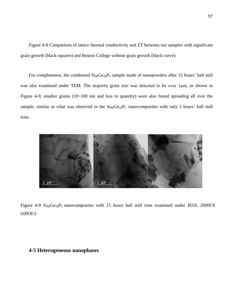
97
Figure 4-8 Comparison of lattice thermal conductivity and ZT between our samples with significant
grain growth (black squares) and Boston College without grain growth (black curve).
For completeness, the condensed Si80Ge20P2 sample made of nanopowders after 15 hours’ ball mill
was also examined under TEM. The majority grain size was detected to be over 1μm, as shown in
Figure 4-9; smaller grains (10~100 nm and less in quantity) were also found spreading all over the
sample, similar as what was observed in the Si80Ge20P2 nanocomposites with only 5 hours’ ball mill
time.
Figure 4-9 Si80Ge20P2 nanocomposites with 15 hours ball mill time examined under JEOL 2000FX
(a)(b)(c).
4-5 Heterogeneous nanophases
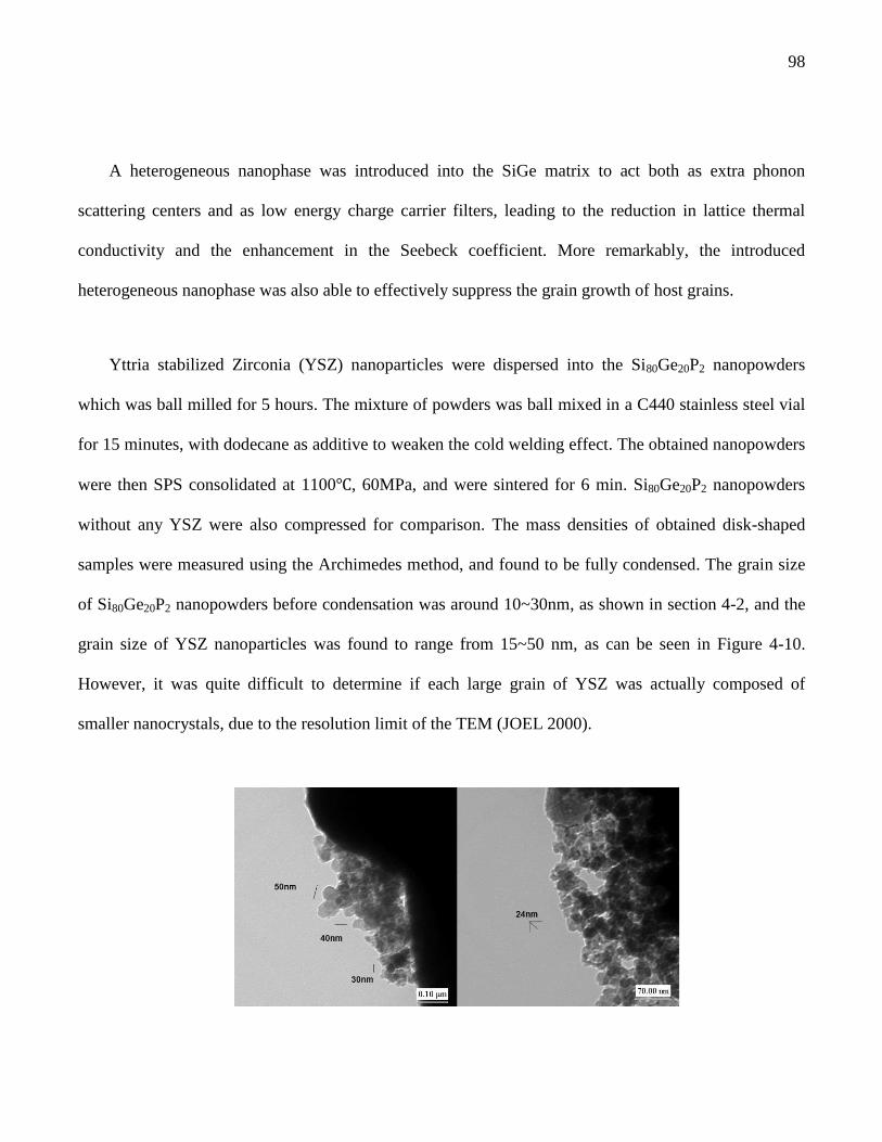
98
A heterogeneous nanophase was introduced into the SiGe matrix to act both as extra phonon
scattering centers and as low energy charge carrier filters, leading to the reduction in lattice thermal
conductivity and the enhancement in the Seebeck coefficient. More remarkably, the introduced
heterogeneous nanophase was also able to effectively suppress the grain growth of host grains.
Yttria stabilized Zirconia (YSZ) nanoparticles were dispersed into the Si80Ge20P2 nanopowders
which was ball milled for 5 hours. The mixture of powders was ball mixed in a C440 stainless steel vial
for 15 minutes, with dodecane as additive to weaken the cold welding effect. The obtained nanopowders
were then SPS consolidated at 1100 , 60MPa, and were sintered for 6 min. Si80Ge20P2 nanopowders
without any YSZ were also compressed for comparison. The mass densities of obtained disk-shaped
samples were measured using the Archimedes method, and found to be fully condensed. The grain size
of Si80Ge20P2 nanopowders before condensation was around 10~30nm, as shown in section 4-2, and the
grain size of YSZ nanoparticles was found to range from 15~50 nm, as can be seen in Figure 4-10.
However, it was quite difficult to determine if each large grain of YSZ was actually composed of
smaller nanocrystals, due to the resolution limit of the TEM (JOEL 2000).

99
Figure 4-10 TEM image of Yttria Stabilized Zirconia (YSZ) nanopowders.
Figure 4-11 TEM images of SPS condensed Si80Ge20P2 nanocomposites (BM for 5hours) with 0% YSZ
(a)(b), 5% YSZ (c)(d) and 10%YSZ (e)(f) nanoparticles.
SPS consolidated samples were examined under TEM. As seen in Figure 4-11(a)(b), significant
grain growth (from 10~30 nm before SPS to ~500 nm after SPS) was observed in the absence of

100
heterogeneous YSZ nanoparticles. However, once 5 vol.% YSZ nanoparticles were dispersed into
Si80Ge20P2 matrix, the grain size in condensed samples was found to be in the same range as that of
corresponding nanopowders, as shown in Figure 4-11(c)(d), indicating nearly no grain growth at all.
Similar phenomenon was also observed in the 10 vol.% YSZ dispersed Si80Ge20P2 sample. While YSZ
nanoparticles helped to effectively impede grain growth, their extremely wide band gap reduced the
overall electrical conductivity; in order to weaken this negative effect, minimal volume fraction of YSZ
nanoparticles should be used, as long as grain growth can be effectively impeded.
In a SiGe matrix with YSZ nanoparticles dispersion, as shown in figure 4-11(c)(d)(e)(f), both dense
larger and light smaller grains were observed. To distinguish them, Energy Dispersive X-ray
spectroscopy (EDS) scanning was applied. Zirconium has two characteristic energy peaks located at
2.2KeV (L1M2) and 15.8KeV (KL3), while phosphorus has a single characteristic energy KM1 peak
located at 2.1KeV. As shown in Figure 4-12, the EDS scanning over the light grains circled in red in
Figure 4-11(c) had two energy peaks at around 2KeV and 16KeV, matching with Zr characteristic peaks;
while scanning over the dense grains only had a characteristic peak at about 2KeV. The results indicated
that light grains were mostly Zr rich YSZ nanograins.
The reason for grain growth being effectively suppressed by heterogeneous nanophase may be
stated as: the incoherent grain boundaries between YSZ and Si80Ge20P2 nanoparticles must be too
difficult to be overcome, even during the SPS consolidation process with high temperature and high
pressure. Grain growth can also be suppressed by the novel core-shell structures which will be discussed
in next section.
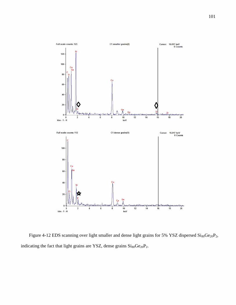
101
Figure 4-12 EDS scanning over light smaller and dense light grains for 5% YSZ dispersed Si80Ge20P2,
indicating the fact that light grains are YSZ, dense grains Si80Ge20P2.

102
Unfortunately, the incorporation of 10% or even 5% YSZ nanoparticles in the SiGe matrix leaded to a
dramatic increase in electrical resistivity, therefore an degradation in power factor, the overall ZT was
found decreased over 15%.
Figure 4-13 Thermal conductivity, power factor and figure of merit ZT of 0%, 2%, 5% and 10% YSZ
nanoparticles dispersed Si80Ge20P2.
4-6 Core-Shell nanostructure
Core–shell nanocrystals are a class of materials whose properties are intermediate between those of
small, individual molecules and those of bulk, crystalline semiconductors. They are unique because of
their easily modular properties, which are a result of their size. These nanocrystals are composed of
a quantum dot core and a shell of a distinct material. Core-shell structure was originally used in

103
fluoroscopy, organically passivated quantum dots have low fluorescence quantum yield due to surface-
related trap states. Core-shell nanocrystals address this problem because the shell increases quantum
yield by passivating the surface trap states.[91] In addition, the shell provides protection against
environmental changes and photo-oxidative degradation. Precise control of the size, shape, and
composition of the core and shell enable the emission wavelength to be tuned over a wider range of
wavelengths than either individual semiconductor. Applications for these materials have been found in
both biological systems and optics.[92], [93]
The novel core-shell structures have also been applied to enhance thermoelectric materials both
theoretically[94] and experimentally.[95] The benefit of nano-sized core-shell structures for TE
materials can be summarized as follows:
(1) In this size regime (~20nm), quantum confinement effects lead to a size-dependent band
gap with observable, quantized energy levels.[91] The quantized energy levels observed in quantum dots
lead to electronic structures that are intermediate between single molecules, which have a
single HOMO-LUMO gap, and bulk semiconductors, which have continuous energy levels within
bands,[96] as shown in Figure 4-14. The enlarged band gap due to quantum confinement is crucial for a
thermoelectric material in that a wider band gap tends to delay the thermal activation of minority carriers,
and thus is able to achieve a higher thermopower at high temperatures.
(2) The incoherent boundaries between quantum dot cores and shell layers make grain growth
extremely difficult. Core nanoparticles are localized and separated from each other by shell layers, while

104
layer material has to expel the core particles in order to grow thicker; both of these difficulties are
almost impossible to be overcome during the consolidation processes.
(3) The shell layers can also act as energy barriers which can filter lower energy charge carriers that
make negative contributions to the Seebeck coefficient.
The properties of semiconducting core-shell structures are based on the relative conduction and
valence band edges alignment of the core and the shell; correspondingly, core-shell structures can be
classified into three types, as shown in Figure 4-15:[91]
Figure 4-14 A enlarged band gap Eg of a quantum dot due to size effect, compared with its bulk
counterpart and single molecule with LUMO-HOMO gap.

105
Type I: the band gap of the core is smaller than that of the shell. Both the conduction and valence
band edges of the core lie within the band gap of the shell, this alignment confines both electrons and
holes in the core, as can be seen in Figure 4-16(a). In this core-shell structure, the thermopower and
electrical conductivity are dominated by the carriers’ density of states (DOS) in CdSe core, while CdS
shells act as energy filters.
Reverse Type I: the band gap of the shell is smaller than of the core, with both conduction and
valence band edges of the shell lying within the band gap of the core; this alignment confines both
electrons and holes in the shell. Therefore, the thermopower and electrical conductivity are determined
by the carrier’s DOS in the shell, while quantum dots of core serve as energy filters and phonon
scattering centers.
Type II: the valence and conduction band edges of the core are either both lower or both higher than
the band edges of the shell. An example of type II is shown in Figure 4-16(b), ZnTe (band
gap~2.26eV)/CdSe (band gap~1.74eV). The effective band gap is thus reduced and counted from the
conduction band edge of CdSe shell to the valence band edge of the ZnTe core.

106
Figure 4-15 Core-shell structures of 3 different types classified by the relative position of conduction and
valence band of the core and the shell, with blue and red blocks represent core and shell band structures
individually.
Figure 4-16 (a) Type I CdSe/CdS core/shell structure and (b) Type II CdSe/CdTe core-shell structure.
It is worth noting that the type II core-shell structure is not effective in improving TE properties,
since the effective band gap of type II is smaller than the band gap of both the core and the shell. As
well known, a narrow band gap is not favorable to achieve high thermopower because it makes the

107
thermal activation of minority charge carrier easier; it is known that minority charge carriers causes
degradation of thermopower via bipolar diffusion.
Several wet chemical methods, such as chemical precipitation, sol-gel, microemulsion and
inverse micelle formation, have been developed to synthesize core shell nanoparticles, with an emphasis
on better control of size, shape, and size distribution. In our case, the sol-gel method was utilized to coat
P-type Si80Ge20B1.7 nanoparticles with Yttria stabilized Zirconia (YSZ), SiO2 and TiO2. TEM image of
consolidated YSZ coated Si80Ge20B1.7 nanoparticles is shown in Figure 4-17, it was found that
nanoscaled (10~30nm) Si80Ge20B1.7 cores were separated from each other by the continuous medium
consisting of smaller YSZ nano-grains. Although this configuration was not a core-shell structure in the
strict sense, it succeeded in suppressing grain growth and filtering low energy carriers, as a real core-
shell should.
Figure 4-17 The pseudo core (red circle)/shell (green circle) structure of Si80Ge20B1.7/YSZ
nanocomposite.
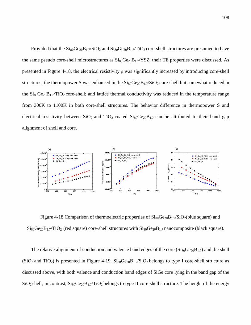
108
Provided that the Si80Ge20B1.7/SiO2 and Si80Ge20B1.7/TiO2 core-shell structures are presumed to have
the same pseudo core-shell microstructures as Si80Ge20B1.7/YSZ, their TE properties were discussed. As
presented in Figure 4-18, the electrical resistivity ρ was significantly increased by introducing core-shell
structures; the thermopower S was enhanced in the Si80Ge20B1.7/SiO2 core-shell but somewhat reduced in
the Si80Ge20B1.7/TiO2 core-shell; and lattice thermal conductivity was reduced in the temperature range
from 300K to 1100K in both core-shell structures. The behavior difference in thermopower S and
electrical resistivity between SiO2 and TiO2 coated Si80Ge20B1.7 can be attributed to their band gap
alignment of shell and core.
Figure 4-18 Comparison of thermoelectric properties of Si80Ge20B1.7/SiO2(blue square) and
Si80Ge20B1.7/TiO2 (red square) core-shell structures with Si80Ge20B1.7 nanocomposite (black square).
The relative alignment of conduction and valence band edges of the core (Si80Ge20B1.7) and the shell
(SiO2 and TiO2) is presented in Figure 4-19. Si80Ge20B1.7/SiO2 belongs to type I core-shell structure as
discussed above, with both valence and conduction band edges of SiGe core lying in the band gap of the
SiO2 shell; in contrast, Si80Ge20B1.7/TiO2 belongs to type II core-shell structure. The height of the energy

109
barriers are determined by the valence band edge difference between the core and the shell. It can be
clearly seen that it is more difficult for holes in the Si80Ge20B1.7 core to transport through the SiO2 shell
than through the TiO2 shell, thus a more significant drop in the hole concentration and eventually a
much higher electrical resistivity are expected in Si80Ge20B1.7/SiO2 than in Si80Ge20B1.7/TiO2. The
effective band gap Eg of the type I Si80Ge20B1.7/SiO2 core-shell stays the same as core SiGe ~0.8eV,
while for Si80Ge20B1.7/TiO2 of type II, the effective band gap is the separation between the valence band
edge of the SiGe core and the conduction band edge of the TiO2 shell, which is < 0.8eV, as shown in
Figure 4-17. Although, low energy holes in SiGe core are filtered by the TiO2 energy barriers, ideally
leading to an enhanced thermopower, the reduced effective band gap make thermal activation of
minority carriers much easier; these two effects together explains the thermopower reduction in
Si80Ge20B1.7/TiO2. Introduced core-shell structures also increase the intensity of phonon scattering,
regardless of their type, resulting in the reduction of lattice thermal conductivity, as presented in Figure
4-18(c).

110
Figure 4-19 Conduction and valence bands alignment of SiGe core and SiO2/TiO2/YSZ shell.
Although grain growth was suppressed in the core-shell structures discussed above, however, the
electrical resistivity was significantly increased since a decent number of charge carriers were filtered by
the thick YSZ shells, the increase in electrical resistivity is so significant that the benefits gained in
thermopower, thermal conductivity couldn’t even compensate, eventually leading to a degradation in
overall ZT as shown in Figure 4-20. The fabrication technique has to be improved to construct much
thinner shells around core materials.
Figure 4-20 Figure of merit ZT in Si80Ge20B1.7/SiO2 and Si80Ge20B1.7/TiO2.

111
The discussions above suggest that core-shell structures which can be used to improve the TE
properties should be limited to type I, and that the difference of conduction/valence band edges between
the core and the shell needs to be restricted to a mild level; only in this circumstance, can enhancement
in the thermopower, and reduction in the thermal conductivity be achieved simultaneously, eventually
results in the enhancement in figure of merit ZT.
4-7 Conclusions and future work
N-type Si80Ge20P2 and P-type Si80Ge20B1.7 nanocomposites were synthesized using high energy
vibrational ball mill method, followed by SPS consolidations. The dependence of the grain size of
obtained nanopowders on ball mill time was investigated, and it was found that five hours was sufficient
to obtain nanograins of 10~30nm; extended ball mill time did not show evidence of further reducing the
grain size. During the SPS consolidation process, porosity due to insufficient sintering temperature was
found to be fatal to TE performance; although thermopower S and thermal conductivity κ may be
enhanced via energy filtering effect and enhanced phonon scattering respectively, the benefit gained in S
and κ was not able to compensate for the significant loss in the electrical conductivity. It was also found
that severe grain growth took place during the SPS consolidation process; the characteristic grain size in
condensed SiGe bulk samples was as large as 500nm~1μm, while it had been only 10~30nm in SiGe
nanopowders before SPS consolidation. Despite the grain growth, we managed to obtain the figure of
merit ZT~1.2 in N-type Si80Ge20P2 and ZT~0.75 in P-type Si80Ge20B1.7 both at 1123K. The significant
112
grain growth could be attributed to the relatively small mismatching potentials or coherent interfaces
between SiGe nanograins; thus, we suggested suppressing grain growth by introducing incoherent grain
boundaries. Heterogeneous nanophase as well as core-shell structures were performed at this point and
both were proved to be capable of effectively suppress the grain growth in the SPS consolidation
processes; moreover, enhanced phonon scattering intensity as well as energy filtering effects were also
observed.
Significant degradations in electrical conductivity were observed upon using nano-sized oxides
either as external phases or pseudo shell materials, due to the oxides’ extremely wide band gaps. In the
future, investigations should be performed in finding proper materials which have proper band structure
alignments with Si80Ge20 host in order to introduce incoherent or semi-coherent interfaces to impede
grain growth without affecting the charge carrier transport. Exploration in fabrication techniques to
construct core-shell structures with much thinner shells should also be conducted.

113
5. Effective Medium Theory
To simulate the lattice thermal conductivity reduction effect due to nanoinclusions, deterministic
solutions of phonon Boltzmann transport equation (BTE),[97], [98], [99], [100] Callaway model[57],
[101] derived from BTE and Monte Carlo simulations with either frequency independent gray
model[102] or the non-gray model[77],[103] have been developed. There are also first-principles
calculations, using a Kubo-Greenwood style approach, accounting for disorder-induced scattering that
many other models which are based on the Peierls-Bolztmann equation, coherent potential
approximation, or atomic models failed to take into account.[21],[97] Nevertheless, even the most
simplified ab-initio/first principles calculation requires extensive modeling and computing time,
restricting its extensive applications. A phenomenological effective medium approach (EMA) by Nan et
al.[104],[105] provided an alternative way to study two-phase heterogeneous systems. Incorporated
within the average T-matrix approximation (ATA), Minnich and Chen[106] proposed the modified
effective mean free path (MFP) for both matrix and second-phase materials. The modification came
from phonons’ independent particle scattering off embedded nanoparticles, in addition to thermal
boundary resistance. However, this ATA was based on first-order T-matrix approximation, thus only
applicable in small volume fractions. Poon et al. extended this effective medium approach to the whole
volume fraction range from 0 to 1 by introducing a differential effective medium (DEM) method[107],
[108] with multiple scattering that dominates at high volume fractions being inherently implemented.
114
Prior experiments[53], [85], [109] have indicated a dramatic reduction in lattice thermal
conductivity κph even with only a small volume fraction of nanoinclusions, which is unable to be well
explained by various effective medium theories (EMT) mentioned above. The disagreement between
models and experimental data strongly indicates that the grain boundary scattering effect was
underestimated, especially at low volume fractions. One possible reason for this underestimation of
interface scattering is that the scattering cross section of an embedded nanoparticle was believed to be
the spherical particle’s projected area π(d/2)2 in previous works.[106], [107], [108] Inspired by Kim et
al.,[110] we implemented the much more rigorously calculated effective scattering cross section σeff, as
well as grain size dispersion, into DEM simulation to achieve a better agreement with both the MC
simulation by Jeng[102] and the experimental results.[111]
5-1 Average T-Matrix Approximation (ATA) and Coherent Potential
Approximation (CPA)
5-1-1 ATA
The effective medium theory is adopted to deal with the effective thermal conductivity in a
heterogeneous system. Following Nan’s work, the effective thermal conductivity k* of a heterogeneous
system can be deduced from the following set of equations:
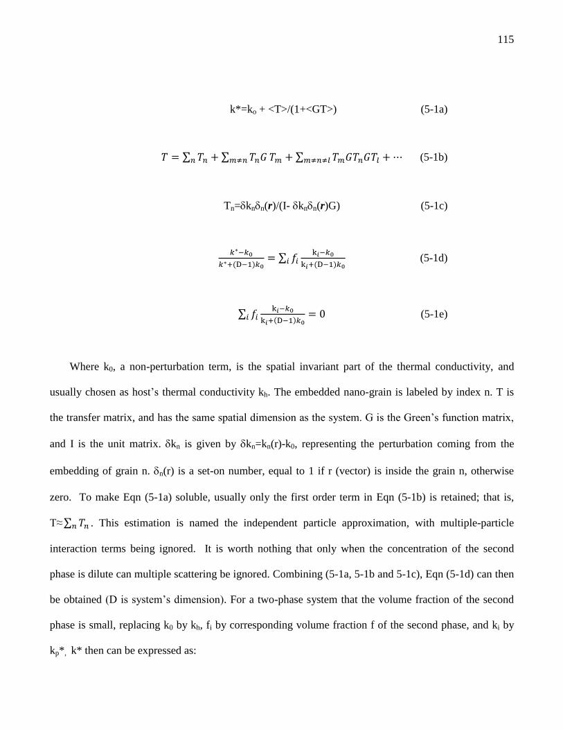
115
k*=ko + <T>/(1+<GT>) (5-1a)
∑ ∑ ∑ (5-1b)
Tn=knn(r)/(I- knn(r)G) (5-1c)
( ) ∑
( ) (5-1d)
∑
( ) (5-1e)
Where k0, a non-perturbation term, is the spatial invariant part of the thermal conductivity, and
usually chosen as host’s thermal conductivity kh. The embedded nano-grain is labeled by index n. T is
the transfer matrix, and has the same spatial dimension as the system. G is the Green’s function matrix,
and I is the unit matrix. kn is given by kn=kn(r)-k0, representing the perturbation coming from the
embedding of grain n. n(r) is a set-on number, equal to 1 if r (vector) is inside the grain n, otherwise
zero. To make Eqn (5-1a) soluble, usually only the first order term in Eqn (5-1b) is retained; that is,
T≈∑ . This estimation is named the independent particle approximation, with multiple-particle
interaction terms being ignored. It is worth nothing that only when the concentration of the second
phase is dilute can multiple scattering be ignored. Combining (5-1a, 5-1b and 5-1c), Eqn (5-1d) can then
be obtained (D is system’s dimension). For a two-phase system that the volume fraction of the second
phase is small, replacing k0 by kh, fi by corresponding volume fraction f of the second phase, and ki by
kp*, k* then can be expressed as:
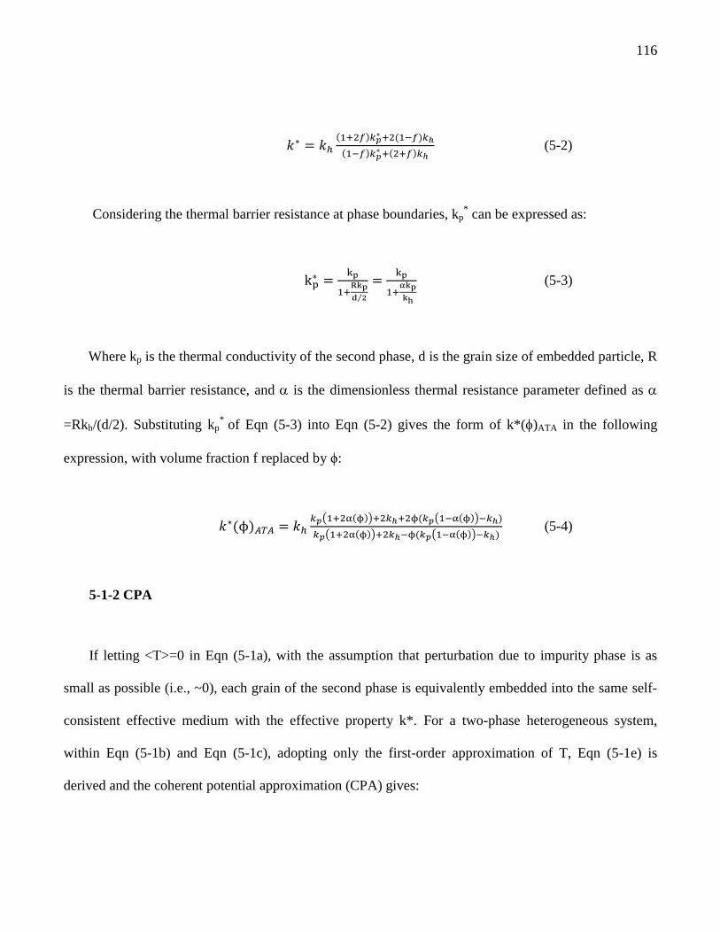
116
( ) ( )
( ) ( )
(5-2)
Considering the thermal barrier resistance at phase boundaries, kp* can be expressed as:
⁄
(5-3)
Where kp is the thermal conductivity of the second phase, d is the grain size of embedded particle, R
is the thermal barrier resistance, and is the dimensionless thermal resistance parameter defined as
=Rkh/(d/2). Substituting kp*
of Eqn (5-3) into Eqn (5-2) gives the form of k*()ATA in the following
expression, with volume fraction f replaced by ϕ:
( ) ( ( )) ( ( ( )) )
( ( )) ( ( ( )) ) (5-4)
5-1-2 CPA
If letting <T>=0 in Eqn (5-1a), with the assumption that perturbation due to impurity phase is as
small as possible (i.e., ~0), each grain of the second phase is equivalently embedded into the same self-
consistent effective medium with the effective property k*. For a two-phase heterogeneous system,
within Eqn (5-1b) and Eqn (5-1c), adopting only the first-order approximation of T, Eqn (5-1e) is
derived and the coherent potential approximation (CPA) gives:

117
2k*CPA2-((2-3)kh+(3-1)kp*)k
*CPA-khkp*=0 (5-5)
Both ATA and CPA account for the first order independent particle scattering and thus can only be
applied in the system that the volume faction of second phase is dilute. The difference between them is
that CPA allows particle clusters, while ATA requires an even distribution of second-phase particles in
the main matrix.
5-2 Differential Effective Medium (DEM) approach
The application of ATA is restricted to the systems where the second phase has low volume
fractions, as seen from the deduction process discussed above. To extend ATA to the heterogeneous
systems with higher volume fractions of second phase, the differential method, as discussed by
Bruggeman,[112] is then implemented to Eqn (5-4). For convenience, the effective thermal conductivity
k* is replaced by k hereafter. The main idea of this differential approach is that, at volume fraction , kh
is updated to the instantaneous effective thermal conductivity k(/(1- d)), since the volume d to be
occupied by the added particles does not contribute to kh(), as shown in Figure 5-1; upon adding d of
particles to the new host, the overall effective thermal conductivity is then k(ϕ+dϕ). k(/(1- d)) can be
expanded into k()+k()d, or k()+dk() with first-order approximation. The updated host
conductivity is expressed as:

118
kh() k()+dk() (5-6)
Figure 5-1 Configuration of adding dϕ of second phase in DEM regime.
Upon introducing the second-phase nanoparticles, the effective mean free path (MFP) of host and
second phase has to be modified as follows:[106]
{
(5-7)
Where Lsct=V/σeff=πd3/(6ϕσeff), V is the mean volume containing only one nanoparticle, d is the
mean diameter of the spherical nanoparticles, ϕ is the volume fraction of nanoparticles, and σeff is the
effective scattering cross section of the nanoparticle. For hard sphere scattering in the independent-
particle approximation, σeff is assumed to be the spherical particle’s projected area πd2/4; thus, the host’s
thermal conductivity is given by the renormalized function kh(f)=kh/(1+3Lhf/2d), where f is the
targeted filling fraction. In the differential approach, kh(+d)=kh()/(1+3Lh()d/2d)=

119
kh()/(1+(3Lh()f/2d)(d/f)). For other forms of phonon-particle scattering other than independent-
particle scattering, the scattering function 3ϕ/2 can be replaced by F(ϕ); kh() may then be written as
kh()=kh/(1+LhF()/d) in the first-order approximation and the updated thermal conductivity of the new
host:
kh(+d) = kh()/(1+Lh()F(f)(d/f)/d) (5-8)
Substituting Eqn (5-6) in (5-8), keeping only the first order terms and replacing Lh() by L(),
which is 3k()/(vgcp), where vg is the average group velocity, and kh(+d) can be written as:
( ) ( ) ( ) ( ) ( )
( )
(5-9)
Upon adding d particles to the composite, k(+d) can be written like Eqn (5-4):
( ) ( ) ( ( )) ( ) ( ( ( )) ( ))
( ( )) ( ) ( ( ( )) ( ))
(5-10)
Substituting Eqn (5-6) and Eqn (5-9) into Eqn (5-10), keeping only the first order term, k(+d)
becomes:
( ) ( ) ( ) ( ) ( )
( )
( )
( ( )) ( )
( ( )) ( )
120
(5-11)
Rearranging the terms, the following differential form of k() is obtained:
( ) ( )
{
( ( )) ( )
( ( )) ( )
() ( )
} (5-12)
The effective thermal conductivity obtained by this method is named k*()DEM in this chapter. The
authenticity of this differential expression is straightforward if one considers only independent-particle
scattering; if we let F()=3/2, Eqn (3) in reference 107 is obtained. The DEM approach is a decent
improvement over ATA, not only because it extends ATA to the full volume fraction range from 0 to 1,
but also it is able to inherently implement multiple scattering with well selected F(ϕ), as to be discussed
later.
5-3 Comparison between DEM and ATA
As discussed above, ATA is derived from small perturbation theory: the embedded particle in
consideration is taken as a small perturbation, while matrix material is considered a homogeneous
effective medium without considering the effect from other embedded particles; therefore, ATA only
hold physical meanings at low volume fractions of the second phase. For DEM, again, the embedded
particle in consideration is taken as a perturbation; however, in this case the effective medium is the
121
combination of host and previously embedded second phase. Thus, the small perturbation holds true for
all the volume fractions from 0 to 1 in DEM. At dilute volume fractions, ATA and DEM do not have
much difference; when the volume fraction ϕ increases to the extent that the small perturbation in ATA
no longer holds, the difference between DEM and ATA will arise.
Without losing generality, independent-particle scattering F(ϕ)=3ϕ/2 is adopted in this section. The
average mean free path l (MFP) can be deduced via the customary method of l=3k/cpvg, where vg is the
average group velocity, cp is the specific heat. At room temperature and above, most phonons are
populated close to the Brillouin zone boundary, where acoustic phonons’ group velocities are
significantly smaller than the speed of sound vs.[113] In this case, a characteristic group velocity is
estimated by averaging vg=vscos(qa/2), where q is the wavenumber and a is the crystal lattice constant,
over the phonon spectrum,[107], [108] yielding approximately 0.38vs. Considering the difficulty of
obtaining a complete series of parameters for a certain composite, some estimated equations are also
utilized to figure out unknown parameters.
Debye Temperature θD:[114]
(
)
(5-13)
Sound velocity vs:

122
{
√
√
(5-14)
Where h is the Plank constant, k is the Boltzmann constant, n is the number of atoms in unit cell, V
is the volume of unit cell, G and E are shear and Young’s modulus, respectively, and ρ is the mass
density.
Table 5-1 The parameters used in nanocomposite calculations for DEM and ATA. [86], [115], [116], [117],
[118]
composites Debye D(K) κbulk(W/(m*K))
Cp(10
6J/m
3K) Vs(m/s) Vg(m/s) MFP(nm)
YSZ/CoSb3 527/307 1.8/14.5 3.27/1.79 3737/2998 1420/1139 1.16/21.3
CoSb3/CoSb3 307/307 14.5/14/5 1.79/1.79 2998/2998 1139/1139 21.3/21.3
DEM and ATA calculations are performed on two nanocomposites; one is inert Yttria Stabilized
Zirconia (YSZ) nanoparticles embedded in skutterudite CoSb3, and the other is a fictional nanostructure
with CoSb3 nanoparticles being embedded in a CoSb3 matrix. The grain sizes of nanoparticles in both
nanocomposites are varying from 50 nm to 5 nm.

123
Figure 5-2 Dependence of lattice thermal conductivity κph in YSZ/CoSb3 nanoparticle/matrix
system on volume fraction ϕ at 300K, with DEM (solid lines) and ATA (dash lines) calculations; the
grain size of YSZ nanoparticles are set to be 50, 20, 20, 5 nm separately.

124
Figure 5-3 Dependence of lattice thermal conductivity κph in a CoSb3/CoSb3 nanoparticle/matrix
system on volume fraction ϕ at 300K, with DEM (solid lines) and ATA (dash lines) calculations; the
grain size of YSZ nanoparticles are set to be 50, 20, 20, 5 nm separately.
It can be seen from Figure 5-2 and Figure 5-3 that, for both ATA and DEM, as the volume fraction
ϕ of nanoparticles increases, the lattice thermal conductivity decreases significantly. At the same volume
fraction, nanoparticles of smaller size have a better effect on obstruct phonon transport, because a
smaller particle size corresponds to a higher interface density and lower effective phonon MFP, thus a
lower effective lattice thermal conductivity. Indeed, nanostructuring is an impressive way to reduce
lattice thermal conductivity; at d=5nm, with only 20% YSZ nanoparticles embedment, κph is reduced by
60%. As discussed above, ATA actually holds physical meaning only at low volume fractions; as long

125
as small perturbation theory is valid, there should be little difference between ATA and DEM. The
calculations shown in both figures at various grain sizes confirm this deduction; in both nanocomposites,
only when volume fraction ϕ exceeds 10%, will considerable differences arise between ATA and DEM.
In the YSZ/CoSb3 system, at grain size 50 nm, the DEM calculation does not start to diverge from ATA
until ϕ is over 80%!
It is interesting to see that, the smaller the grain size d is, the lower is the volume fraction ϕ needed
to observe the divergence of DEM and ATA. The divergence arises at a threshold where small
perturbation theory cannot apply, as previously discussed. This threshold is evaluated in term of volume
fraction, however, considering that the lattice thermal conductivity reduction actually comes from
interface scattering, it is more plausible to use interface density instead of volume fraction.[106] At the
same volume fraction, smaller grains result in higher interface density, thus more intense phonon
interface scattering. A re-plot of lattice thermal conductivity vs. interface density in the YSZ/CoSb3
nanocomposite system is presented in Figure 5-4, in which the interface density Φ is calculated in the
case of spherical particles:
( )
( )
(5-15)
It can be seen that the divergence of DEM and ATA starts at more or less the same interface density
Φ, as marked with an olive vertical dash line, indicating that the interface density instead of the volume
fraction is the determinate factor of evaluating the intensity of grain boundary scattering.

126
Figure 5-4 Lattice thermal conductivity dependence on interface density Φ, in YSZ/CoSb3
naoncomposite at 300K, the grain size is equal to 50,20,10 and 5 nm separately.
Both ATA and DEM discussed above deal only with independent-particle scattering, without
considering multiple scattering effect, as shown in Figure 5-5. As the volume fraction ϕ of second phase
increases, modification has to be made to account for the important multiple scattering effect.

127
Figure 5-5 Independent-particle scattering in low volume fractions vs. multiple scattering in high
volume fractions.
5-4 DEM with inherently implemented multiple scattering
Presented in Figure 5-5 are configurations of independent scattering at dilute volume fractions and
multiple scattering at high volume fractions. At high volume fractions, the configuration can be taken as
the core-shell structure as discussed in chapter 4. The core-shell configuration can be formulated by
replacing the host materials with nano-inclusions gradually. As the amount of these nanoinclusions
increases, the matrix material eventually behaves like shells surrounding the nanoparticles.
The average thickness of the shells is evaluated by the parameter t, which is defined as t=d(1-
ϕ1/3
)/ϕ1/3
. This definition comes from the approximate volume fraction of the spherical nano-inclusions
ϕ=(d/(d+t))3. As the volume fraction ϕ increases, the average thickness t of the shells decreases; phonon-

128
particle scattering in the host thus occurs more often within the inter-particle region. At this point,
multiple phonon-particle scattering has to be considered and the relevant length scale that determines the
scattering rate then changes from d to t. Qualitatively, there exists a crossover volume fraction 0, above
which 1/d<1/t. For <<o, the scattering is mostly independent-particle scattering and F(ϕ) is 3ϕ/2.
For >o, inter-particle boundary scattering becomes important. Setting t=d, 0 is found to be ~0.125.
Detailed calculation based on the spatial occupancy of particles and particle shape yields 0 in the range
from ~0.1 for polyhedral dispersoids to ~0.2 for spherical dispersoids[107]. Considering experimental
systems, it is feasible to adopt 0 ~0.15 as a decent approximation. As ϕ keeps increasing and t becomes
smaller than the phonon wavelength h, the host no longer plays a significant role. This discussion
allows for the alteration of the scattering function F(ϕ) to the following form.
() [
(
)] ( (
( )
)
) (5-16)
This expression maintains the initial independent-particle scattering mechanism of F(ϕ)=3/2 at low
volume fractions, changes to F(ϕ)=d/t beyond the crossover point 0, and approaches zero as 1.
Figure 5-6 shows the comparison between F(ϕ) in the form of Eqn (5-16) and the independent-particle
scattering of 3ϕ/2 for Si/ZrO2 core-shell with particle size d~10nm. It can be expected that multiple
phonon-particle scattering shall have a better suppression effect on lattice thermal conductivity than
independent-particle scattering approximation, at both intermediate and high volume fractions.

129
Figure 5-6 Comparison between multiple scattering and independent-particle scattering 3ϕ/2.
In Eqn (5-16), the characteristic wavelength h was introduced to discuss the phonon scattering at the
point when the length scale t is comparable with the phonon wavelength of the host. In the gray model,
h is independent on phonon frequency, considering ω~sin(qa/2), vg~vscos(qa/2), density of states D(q)~
4πq2, and the characteristic phonon wavelength of the host can be estimated over the phonon spectral
function as follows:
∫
∫
∫
(
)
∫
(
)
( ) (5-17)
Where a is the lattice constant, and the typical characteristic wavelength of the host is around 2 nm.

130
It is straightforward for one to choose the core and the shell materials so that they are chemically
stable at operating temperatures and not soluble in each other. ZrO2 and Yttria-stablized-Zirconia (YSZ)
are extremely unreactive and therefore are widely used as core or shell material. It is worth nothing that
these embedded nano-inclusions not only serve as phonon particle scattering centers but also play a
significant role in suppressing grain growth of the host materials.
Effective lattice thermal conductivity of Si/ZrO2 and Si80Ge20/YSZ core-shell nanostructures are
presented in Figure 5-7 and Figure 5-8. Solid lines are DEM calculation with F(ϕ) in Eqn (5-16), which
inherently incorporates multiple scattering, while dashed lines indicate DEM calculation with
F(ϕ)=3ϕ/2, with independent-particle scattering assumption. The scattering intensity of Eqn (5-16) is
compared with that of independent scattering as shown in Figure 5-6, at most volume fractions except
the ending point where ϕ~1, multiple scattering should be more effectively than single particle
scattering. Closely packed core particles provide the configuration for multiple particle scattering, and
hence cause more remarkable reduction in lattice thermal conductivity than the independent particle
scattering approximation. Indeed, as shown in Figure 5-7 and Figure 5-8, DEM calculation with
inherently implemented multiple scattering effects always has lower lattice thermal conductivity than its
counterpart with F(ϕ)=3ϕ/2. As ϕ increases from 0 to ϕ0~0.15, the concentration of nano-inclusions is
still dilute, only independent-particle scattering needs to be considered. As ϕ keeps increasing, the
distance between embedded particles decreases and multiple phonon-particle scattering starts to
dominate, as represented by the term (1-exp(-ϕ/ϕ0)). It is interesting to observe a minimum value of
thermal conductivity close to the point of ϕ~1. The scattering can assumed to be hard-sphere scattering
as long as the width of the inter-particle distance t and the particle size d satisfy t>>λh and d>>λh.

131
However, as the scattering length scale (t or d) decreases to the point where phonons with wavelength λh
can no longer penetrate, the thermal conductivity will vanish,[119] which unfortunately conflicts with
realistic physical observations; the last factor 1-exp(-(t/λh)2) in Eqn (5-16) was thus introduced to avoid
this contradiction. At different particle size d, the minimum lattice thermal conductivities correspond to
different volume fractions ϕ, but they are all at almost the same shell thickness t, as shown in Figure 5-7
and Figure 5-8. This indicates that, at this region, it is the length scale t that determines the scattering
mechanism. When the length scale of the system is even smaller than the average phonon wavelength,
hard-sphere scattering is no longer valid, and the scattering mechanism will approach Rayleigh
scattering regime. The authenticity of this introduced factor 1-exp(-(t/λh)2) is still pending, but it
provided an intuitive picture that a minimal lattice thermal conductivity can be reached at some shell
thickness t close to h. Rigorous calculations must be conducted in the future to ascertain the scattering
mechanism at this length scale.
Table 5-2 Parameter used in the core-shell systems of Si/ZrO2 and Si80Ge20/YSZ, at T=1100K.
composites
Debye
D(K)
κbulk(W/(m*K))
Cp(106J/m
3K) Vs(m/s) Vg(m/s) MFP(nm)
Si/ZrO2[103], [108] 645/590 31.2/2.2 2.07/3.58 5961/3591 2265/1365 19.96/1.35
Si80Ge20/YSZ[108],
[115], [116], [117]
586.8/527 2.6/1.7 2.14/3.27 5166/3737 1963/1420 1.86 /1.10

132
Figure 5-7 DEM Calculated lattice thermal conductivity k*(ϕ)DEM with F(ϕ) in Eqn (5-16)-multiple
scattering and F(ϕ)=3ϕ/2-independent particle scattering in core-shell structure of Si/ZrO2 at grain size
d=50, 20, 10 and 5 nm.

133
Figure 5-8 DEM Calculated lattice thermal conductivity k*(ϕ)DEM with F(ϕ) in Eqn (5-16)-multiple
scattering and F(ϕ)=3ϕ/2-independent particle scattering in core-shell structure of Si80Ge20/YSZ at grain
size d=50, 20, 10 and 5 nm.

134
At the ending point where ϕ=1, a monolithic nanostructure composed solely of core nanoparticles
is formed; the exact value of its effective lattice thermal conductivity can then be derived from Eqn (5-
12). The different ending points in DEM using multiple scattering function and independent particle
scattering can be explained as follows. As ϕ 1, in the case of multiple scattering F(ϕ)=Eqn (5-16), the
second term in the parentheses diminishes. The convergence of dk(ϕ) at ϕ=1 then requires the numerator
of the first term in the parentheses to be zero:
( ( )) ( ) (5-18)
Where kp=kp0/(1+lp/d), and thermal resistance parameter α(1)=kh(1)R(1)/(d/2). Considering ϕ=1,
kh(1)=k(1), R(1)=4(cpvp+cpvp)/cpvpcpvp=8/cpvp=8lp/3kp0, [113] Eqn (5-18) can then be written as:
( ( )
) ( ) (5-19)
With the terms arranged, k(ϕ) at ϕ=1 can eventually be obtained:
( )
(5-20)
The lattice thermal conductivity of the monolithic nanostructure has nothing to do with the host
materials, and it decreases monotonically as the grain size d decreases.
135
For independent particle scattering, when F(ϕ)=3/2 at ϕ=1, similar calculations give the ending
point of the monolithic nanostructure as:
( )
√(
)
(
) (
)
(
)
(5-21)
Although the novel core-shell structure helps to suppress the lattice thermal conductivity of TE
materials by increasing the phonon-boundary scattering, the existence of the heterogeneous phase and
associated defects can also impede charge carriers’ transport, resulting in an increased electrical
resistivity and might eventually leading to a reduced overall ZT. One possible solution is to use the same
material for both cores and shells; that is, to construct the nanocomposite with a mixture of nano-sized
grains with different grain sizes. An alternative is to generate in-situ nanoparticles via phase segregation,
since in-situ formed nanophase has close electrical and thermal properties to those of the matrix
material; in this case, the effect of incoherent boundaries between the core and the shell to impede
charge carriers’ transport is thus weakened. Examples of in-situ formed Full Heusler/Half Heusler and
PbSe/PbS nanocomposites will be discussed in the next section.
5-5 Effective scattering cross section

136
The prerequisite of hard particle scattering assumption is that the scattering length scale (t or d) is
much larger than the characteristic wavelength λh (~2nm); based on this assumption, the scattering
cross-section of an embedded spherical nanoparticle is its projected area πd2/4. Corresponding
calculations are presented in the last sections, both in independent-particle scattering regime and
multiple scattering regime. However, the dramatic drop in lattice thermal conductivity observed in
experiments, especially at low volume fractions of a second phase, doesn’t match the simulations above
very well; thus, phonon scattering must still be underestimated to some extent. Inspired by Kim et
al.,[110] we implemented the much more rigorously calculated effective scattering cross section σeff, as
well as grain size dispersion, into the DEM simulation to achieve a better agreement with both the MC
simulation by Jeng[102] and the experimental results.[111]
5-5-1 Scattering cross section
The Mie solution to Maxwell’s equation[120], [121] depicts that when electromagnetic waves
encounter spherical particles the scattering cross section varies from ~ω4 of Rayleigh regime to
frequency independent geometric regime (Rayleigh-Gans-Debye scattering) as size factor χ=qR (R is the
wave number, and R the particle radius) changes from one extreme of χ 1 to the other of χ ~ . Ying
and Truell et al. [122], [123] extended this treatment and derived the scattering cross section of a
phonon wave off spherical particles in a solid. Despite the relative simple form of cross sections σeff for
the two extreme cases, it is fairly difficult to establish relationships between σeff and the scattering
parameters in a more general case, where particle size d is comparable with the incoming wavelength λ,

137
due to the mathematical complexity. Majumdar[124] bridged the scattering cross section of two
extremes and proposed the effective cross-section σeff for the intermediate χ to be :
(
)
(5-22)
As the size factor χ 0, and the particle size d incoming wavelength λ, Eqn (5-22) becomes σsct
π(d/2)2χ
4 ~ ω
4, which is exactly the Rayleigh scattering; while χ , and λ d, resulting in a
frequency independent cross-section σsct π(d/2)2 in the near geometric scattering regime. This method
is correct in describing the two extreme cases, but insufficient to depict the vibration behavior of
scattering cross section at an intermediate size factor χ. Kim and Majumdar, in a later work,[110]
rigorously calculated scattering cross section in two extreme regimes and suggested to bridge them
together as:
(5-23)
The effective cross section in the Rayleigh regime σRayleigh is shown to be proportional to χ4 with the
magnitude determined by mass and force difference ( and respectively) between
embedded and host materials and, when χ approaches 0, σRayleigh ~ χ4 0, as the Rayleigh limit does. The
second term σnear-geometric accounts for the near geometric regime scattering, and its strength is
proportional to 2π(d/2)2 multiplied by an oscillating factor, which approaches 1 when χ 1. Scattering in
the near geometric regime was first well studied by van de Hulst[121] for electromagnetic waves. The
total effective scattering cross section σtotal, determined by the inverse sum of cross sections at two

138
extreme regimes, approaches 0 when χ is infinitesimal and increases to a certain value before starting to
oscillate with χ. The oscillating factor then fades away as χ increases and eventually σtotal retains around
2π(d/2)2. A more intuitive plot is well presented by Kim and Majumdar,[110] which is validated by our
calculation. It is worth noting that the scattering cross section reaches twice the projected area of a
spherical nanoparticle at χ , which can be understood in the sense that scattering always occurring
at the edges of the nanoparticles enlarges the scattering cross section due to diffraction.[120]
To calculate the effective scattering cross section at certain particle size factor χ, the wavenumber
q=χ/d needs to be evaluated. For acoustic phonon branch, the group velocity is given by vg~vscos(qa/2)
and the frequency ω~sin(qa/2), where vs is sound speed at q=0 and a is the lattice constant. The average
wavenumber in host material can then be estimated by averaging vg over the phonon spectrum D(q) or
spectral function D(q)<n> ~ q2/(exp( ω/kT)-1), where D(q)=4πq
2 is the phonon density of states and
<n>=1/(exp( ω/kT)-1) the phonon distribution function:
{
∫
∫
∫
(
)
∫
(
)
( )
∫
∫
(5-24)
Calculated average wavenumbers (q~2.25/a) for several composites are listed in Table I. In realistic
systems, acoustic phonons, which dominate heat transfer at temperature of interests (300~1200K), bear a
characteristic wavelength λ ~ 2 nm. The relative small value of λ when compared with the nanoparticle
size (generally greater than 3~5 nm), eventually yields σeff σnear-geometric, as a fair approximation.
139
5-5-2 Grain size dispersion
Experiments have shown that nanoparticle sizes in most nanocomposites spread from a few to
hundreds of nanometers[125], [126] rather than being fixed at constant value as used in models. In
theory, a system of nanoparticles containing a wide size dispersion is capable of scattering off phonons
of different wavelengths over the spectrum thus rendering it more effective than its counterpart with a
constant grain size.[11] Jeng et al. [102] argued that further randomness of grain size distribution
doesn’t help to reduce lattice thermal conductivity with MC simulations, which is fairly true to some
extent, however, in later simulations, scattering cross section increases at a larger grain size standard
deviation, eventually leads to a considerably lower κph. The effective scattering cross section with a
normalized grain size distribution function F(x) can be expressed as:[110]
∫ ( ) ( )
(5-25)
where dmin and dmax are the lower limit and upper limit of grain size individually. Presented in Table
II are 5 distribution functions and their corresponding effective scattering cross sections. F1 is for
nanoparticles with a constant diameter, F2 and F3 are even distributions over different ranges, F4 and F5
are normalized Gamma distributions with ab = mean diameter d0 and a1/2
b = standard deviation (shape
parameter a=12, scale parameter b=d0/12 in F4; a=3, b=d0/3 in F5). F2 and F3 are presented in order to
show that it is universal that grain size dispersion results in increased effective scattering cross section.
In this article, Gamma distributions of F4 and F5 are adopted without losing generality.

140
Table 5-3 – Size dispersion function dependence effective scattering cross section for
ErAs/In0.53Ga0.47As nanocomposite with average ErAs grain size d0=10nm. F1 is a delta function, F2 and
F3 are even distributions, and F4 are F5 are Gamma distributions with shape parameter a=12, scale
parameter b=d0/12 and a=3, b=d0/3 respectively. (a)
Numerical calc. by Eqn(5-25), (b)
simplified σeff*
in
Eqn(5-26).
Distribution
Function F(x) diameter size range stdev
numerical calc.(a)
σeff/(πd2/4)
Simplified(b)
σeff*/(πd2/4)
Percentage
difference (%)
F1(x)= (x-d) d 0 1.89 2 5.5
F2(x)=
d/2~3d/2
√ 2.31 13/6 6.6
F3(x)=
d/4~7d/4
√ 2.46 19/8 3.6
F4(x) =
( ) 0~
√ 2.16 13/6 0.3
F5(x) =
( ) 0~
√ 2.56 8/3 4.0
The explicit form of Eqn(5-25) is unlikely to be derived due to the complexity of σtotal depending
on spherical particle diameter d or size factor χ, resulting in the inevitability of numerical calculations.
However, for systems whose related parameters (force constants for instance) are unavailable, a
simplification shall then be made to estimate the effective scattering cross section. In most realistic cases,
the lower limit of obtainable grain size is around 3~5nm, with the characteristic average wavenumber q
assumed to be 4 nm-1
(refer to table I), thus χ always lies above 15~20. This lower limit of size factor
falls into the region where scattering efficiency σsct/π(d/2)2
weakly oscillates around 2,[110] hence the

141
approximation of σsct=σnear-geometic=πd2/2 won’t result in a significant deviation from rigorous calculation
via Eqn (5-25). Estimated effective cross section σeff* can then be derived from the simplified integration:
∫
( )
(5-26)
The authenticity of this approximation is validated by comparing explicit integration of Eqn (5-26)
with numerical calculation of Eqn (5-25) in ErAs/In0.53Ga0.47As system discussed by Kim et.al,[110] and
the differences are found to be within 6%, as shown in Table II. The tiny difference between simplified
and rigorous integrations indicates that near geometric scattering dominates phonon scattering for
nanoscaled grains. It is also shown that increasing grain size dispersion tends to result in enlarged
effective scattering cross section, and thus reduced lattice thermal conductivity. A calculation within
Callaway model has depicted similar features.[101]
5-5-3 Validation of effective scattering cross section treatment in DEM
Here, we present the DEM approach with the updated effective scattering cross section calculated
by Eqn (5-26), and show that the calculated results turn out to have a better fit with Jeng et al. gray
model MC simulation.
Parameters used in the DEM calculation are listed in Table 5-1. Presented in Figure 5-9 are
comparisons of various simulations on Si nanoparticles (d0=10nm) embedded Ge bulk matrix. It can be
concluded that (1) Nan’s EMA gives highest effective lattice thermal conductivity, due to not

142
considering grain size effect on interface scattering, (2) DEM simulations with the effective scattering
cross sections discussed above result in faster drops of κph at low volume fractions, compared with
Minnich’s EMA model which utilizes spherical nanoparticle’s projected area πd2/4 as scattering cross
section, (3) DEM simulations with the effective scattering cross sections agree well with Jeng’s gray
model MC simulations, which is supported by experimental results,[127] (4) 15% decrease in κph at
ϕ=0.1 is found in DEM simulations, as the standard deviation of grain size increases from 0 to 5.77nm,
which strongly indicates that nanoinclusions with larger grain size dispersion are more effective in
blocking thermal transfer in a solid.
Table 5-3 Parameters of different composites used in this work, at room temperature T=300K.
composites Bulk κ
(W/mK)
Debye T
θD(K)
cp
(106J/m3K) vs (m/s)
Avg.
vg(m/s)*
MFP
(nm)*
<q>host
(nm-1)*
Lattice
a(nm)
Si/Ge[113],
[128] 150/51.7 645/360 1.66/1.67 6400/3900 2432/1482 110.4/64.1 3.99 0.565
PbS/PbSe[54],
[111], [129] 2.4/1.9 145/141 1.58/1.44 2040/1910 775/726 5.88/5.45 3.67 0.612
FH/HH[130],
[131], [132] 7.2a/10.1 318/390 2.29/2.03 2639#/3498 1003/1329 10.4/11.3 3.68 0.611
FH=ZrNi2Sn, HH=ZrNiSn. *
represent calculated values, a is estimated by κ~1/ρ (this approximated relationship is
derived from experimental data in Ref. [47], [133] ).

143
Figure 5-9 Lattice thermal conductivity κph of Si/Ge nanocomposite dependence on Si nanoparticles’
volume fraction ϕ at 300K, with an average grain size of d0=10nm. DEM simulations with different
grain size dispersions (blue-fixed grain size d=d0, green-standard deviation of 0.289d0 and red-standard
deviation of 0.577d0) are compared with Nan’s EMA (triangles), Minnich’s EMA (black solid line) and
Jeng’s MC simulation (asterisks).
5-5-4 Comparison with PbS-PbSe nanocomposite
Lead chalcogenides, PbTe, PbSe and PbS, have been extensively studied over the past decades as
promising TE materials, mainly due to the unique features of outstanding electrical transport properties
and unusually low thermal conductivities at high temperature. In-situ phase separation process of these
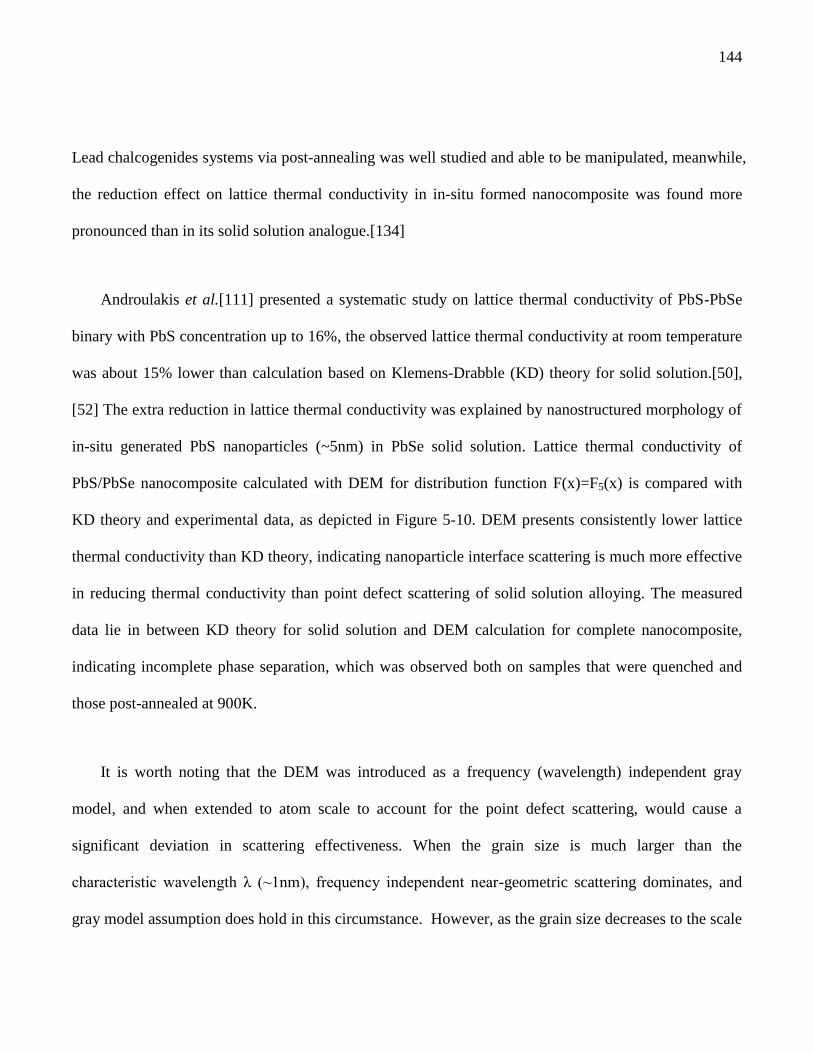
144
Lead chalcogenides systems via post-annealing was well studied and able to be manipulated, meanwhile,
the reduction effect on lattice thermal conductivity in in-situ formed nanocomposite was found more
pronounced than in its solid solution analogue.[134]
Androulakis et al.[111] presented a systematic study on lattice thermal conductivity of PbS-PbSe
binary with PbS concentration up to 16%, the observed lattice thermal conductivity at room temperature
was about 15% lower than calculation based on Klemens-Drabble (KD) theory for solid solution.[50],
[52] The extra reduction in lattice thermal conductivity was explained by nanostructured morphology of
in-situ generated PbS nanoparticles (~5nm) in PbSe solid solution. Lattice thermal conductivity of
PbS/PbSe nanocomposite calculated with DEM for distribution function F(x)=F5(x) is compared with
KD theory and experimental data, as depicted in Figure 5-10. DEM presents consistently lower lattice
thermal conductivity than KD theory, indicating nanoparticle interface scattering is much more effective
in reducing thermal conductivity than point defect scattering of solid solution alloying. The measured
data lie in between KD theory for solid solution and DEM calculation for complete nanocomposite,
indicating incomplete phase separation, which was observed both on samples that were quenched and
those post-annealed at 900K.
It is worth noting that the DEM was introduced as a frequency (wavelength) independent gray
model, and when extended to atom scale to account for the point defect scattering, would cause a
significant deviation in scattering effectiveness. When the grain size is much larger than the
characteristic wavelength λ (~1nm), frequency independent near-geometric scattering dominates, and
gray model assumption does hold in this circumstance. However, as the grain size decreases to the scale
145
of λ, Rayleigh scattering, which strongly depends on phonon frequency, becomes the determining factor,
therefore, the frequency independent gray model is no longer a reasonable assumption. In order to
accurately capture the phonon scattering features at this scale, a frequency (wavelength) dependent non-
gray model is eventually necessary. A possible strategy utilizing DEM to handle the incomplete phase
separation in PbS/PbSe system could be: take the solid solution of host PbSe and dissolved PbS as a
“new host”, whose lattice thermal conductivity can either be obtained from experimental results or KD
theory; meanwhile, treat the undissolved PbS nanoparticles as phonon scattering centers as usual, but of
a smaller volume fraction (total volume fraction subtracts the dissolved portion). Unfortunately, this
strategy is not feasible to be performed in this article, since neither the PbS dissolution ratio nor its
dependence on total PbS volume faction and temperature is available.

146
Figure 5-10 Lattice thermal conductivity κph of PbS/PbSe nanocomposite dependence on PbS
nanoparticles’ volume fraction ϕ at 300K, the comparisons are performed among experimental data
(black asterisks), KD theory for solid solutions (black line) and DEM simulations with grain size
distribution function F5(x) (red line).
While it is comprehensible that incomplete phase separation happens in quenched samples, which to
a great extent retain the solid solution state at high temperature, post-annealed process at a temperature
as high as 900K may cause PbS to partially re-dissolve in PbSe matrix on the other hand. Similar
temperature sensitive re-dissolving process was reported for PbS-PbTe system.[135] Based on the
discussion, post-annealing at a proper temperature to allow thorough phase separation is necessary to
form in-situ nanostructures which can effectively scatter acoustic phonons, leading to reduction in
thermal conductivity and therefore enhancement in dimensionless figure of merit ZT. Further increase of
the second phase, however, won’t lead to a continuous reduction of thermal conductivity, since above
certain volume fraction (for instance, >30% for PbTe/PbS system), nanoparticles of second phase tend to
aggregate into microscale or even larger precipitates,[135], [136] which is not favored for effective
phonon scattering.
5-5-5 Prediction on ZrNi2Sn/ZrNiSn Full Heusler-Half Heusler nanocomposite
Similar to the lead chalcogenides systems,[129] Half Heusler(HH) alloys are also a well-studied
series of TE materials with decent performance at high temperature[40], [41], besides, they are low-cost
and nontoxic. The thermoelectric performance of Half Heusler is mainly limited by its comparably high

147
thermal conductivity. Recently, several interesting works showed improvement on Seebeck coefficient,
electrical conductivity as well as reduction on lattice thermal conductivity by introducing nano-sized
Full Heusler(FH) particles into HH host.[137], [138], [139] However, due to the difficulty in controlling
phase separation in experiments, these researches did not show a systematic reduction in lattice thermal
conductivity as the content of FH phase increases.
Figure 5-11 Dependence of lattice thermal conductivity κph of ZrNi2Sn/ZrNiSn nanocomposite on
ZrNi2Sn nano phase’s volume fraction ϕ at 300K. Two series of plots are presented corresponding to
average grain size d0=5 nm and 10 nm individually, DEM simulations for different grain size dispersions
are distinguished by colors (blue-fixed grain size, green-standard deviation of 0.289d0 and red-standard
deviation of 0.577d0).
148
A prediction based on DEM calculation is presented herein to help quantitatively analyze the
reduction on lattice thermal conductivity one might earn from in-situ nano FH generation in HH matrix,
as shown in Figure 3. Host HH material is chosen to be ZrNiSn, and FH phase ZrNi2Sn, corresponding
parameters used in calculation are listed in Table I. Gamma distribution is utilized to simulate grain size
dispersion with standard deviation of 0.289d0 and 0.577d0 separately, with mean grain sizes d0 set to be
5nm and 10nm. Over 50% reduction on lattice thermal conductivity can be achieved by introducing only
10% ZrNi2Sn nano phases with mean grain size d0 of 5nm, and 40% reduction by d0=10nm. Meanwhile,
electrical conductivity could be enhanced since embedded metallic FH phases also acts as carrier
suppliers. What is more, enhancement on Seebeck coefficient may be gained[137], [138] from the so-
called energy filter effect, specifically, low energy carriers which are believed to be detrimental to
Seebeck coefficient tend to be trapped at the interfaces between nanoparticles and main matrix[140].
Similar trend of reduction on lattice thermal conductivity in TiNi2Sn/TiNiSn nanocomposites was
reported by Birkel et al.[138]
5-5-6 Conclusions
A modified differential effective medium (DEM) calculation with effective scattering cross section
proposed by Kim and Majumdar was conducted to simulate the dramatic lattice thermal conductivity
reduction when nanoparticles are evenly embedded into bulk host materials. It was then validated by
comparing with Monte-Carlo simulation[102] of Si/Ge nanocomposite. The form 2*κDEM-κEMA, which
inherently includes 2nd
order phonon scattering, was recommended to replace the conventional single
particle scattering at low volume fractions. The simulation was then performed on in-situ formed

149
PbS/PbSe nanocomposite, and the calculation was found to be in agreement with reported experimental
results.[111] Finally, prediction on lattice thermal conductivity of ZrNi2Sn(FH)/ZrNiSn(HH)
nanocomposite was made in order to reveal the great promise of reducing lattice thermal conductivity
via introducing secondary FH nanophase.
5-6 Summary and future work of effective medium approach
As an alternative to ab-initio simulations which require extensive computing time, effective medium
approach (EMA), a phenomenological method, is widely used to evaluate the lattice thermal
conductivity of heterogeneous two-phase systems. The derivations of Average T-matrix Approach (ATA)
and Coherent Potential Approximation (CPA) were reviewed. Considering ATA and CPA both being
limited to low volume fractions, a differential effective medium (DEM) was developed to enable
calculation in the full range of second-phase concentrations from 0~1. Furthermore, multiple scattering,
which dominates the high volume fraction region, was inherently implemented in DEM to replace the
previous independent-particle scattering by utilizing scattering mechanism function F(ϕ)=Eqn (5-16)
instead of F(ϕ)=3ϕ/2. This treatment leaded to an interesting minimal lattice thermal conductivity at ϕ
close to 1. The physical meaning was then discussed. Hard particle scattering with scattering cross
section as the projected area of spherical grain A=4π(d/2)2 was widely used, because embedded particles’
grain sizes were much larger than characteristic wavelength of phonons of host in most cases; however,
as the grain size decreases to be comparable with phonon wavelength in host, scattering cross section A

150
needs to be reconsidered. A modification based on rigorous calculations of effective scattering cross-
section was suggested, and the corresponding calculations were found to be close to Monte-Carlo
simulation and experimental results. Some inspiring predictions on in-situ formed Full Heusler/Half
Heusler nanocomposites were proposed to demonstrate the obtainable reduction of lattice thermal
conductivity via nanostructuring technique.
Although DEM with multiple scattering inherently considered is taken as an improvement over
DEM with independent particle scattering, the treatment of phonon scattering at volume fraction ϕ~1 in
Eqn (5-16) still needs further investigation. It is mainly the gray model assumption that phonon
wavelength or frequency is constant causing the inefficiency of DEM in explaining the scattering when
inter-particle distance is extremely small. For future work, a non-gray model shall be implemented into
the DEM calculation, according the frequency dependent scattering cross section; by evaluating the
effective contribution from each frequency via DEM, the total thermal conductivity can be obtained by
integrating over all frequencies provided that the frequency distribution function and phonon dispersion
relations are available.
151
6. Conclusions
Nanostructuring techniques have been utilized to effectively reduce the relatively high lattice
thermal conductivity and to enhance the thermopower in Half Heusler and SiGe alloys. The mechanisms
have been discussed and attributed to the enhanced phonon scattering intensity and the energy barrier
filtering effect respectively. Nanocomposites have been synthesized with high energy mechanic alloying
followed by Spark Plasma Sintering (SPS) consolidations. To conclude, figure of merit ZT=1.0 at 850K
and ZT=0.85 at 1050K were achieved in nanostructured Half Heusler alloys of N-type and P-type
respectively, while ZT=1.2 at 1050K and ZT=0.75 at 1123K were obtained in nanostructured SiGe
alloys of N-type and P-type individually. Severe grain growth might arise during the pulsed direct
current internal heating SPS process, embedding foreign nanophases and constructing core-shell
structures are both proven to be effective means to suppress grain growth, due to introduced incoherent
grain interfaces; however, significant degradation in electrical conductivity arises because the embedded
nanophases are insulating. To solve the problems, our future work can be expanded as follows:
The existence of a foreign nanophase is favorable to achieve low lattice thermal conductivity;
however, direct mixing foreign nanoparticles into the host thermoelectric material usually leads to an
uneven dispersion; specifically, most foreign nanoparticles tend to aggregate at matrix grain boundaries
and can’t effectively scatter acoustic phonons, which dominate heat transport in most temperatures of
interest. Even dispersion of second phase can be achieved by in-situ phase segregations in a solid

152
solution. Like lead chalcogenides (PbTe/PbSe/PbS) systems, in which phase sepregation can be well
manipulated by proper post-annealing processes, in-situ Full Heusler(FH)/Half Heusler(HH)
nanocomposites can also be synthesized via post-annealing processes. Due to the semi-incoherent
interfaces between FH and HH phases, the novel nanostructures should have the promise of reducing
lattice thermal conductivity via grain boundary scattering and enhancing the thermopower via
preferentially scattering the lower energy charge carriers, without highly degrading the electrical
conductivity.
Nanocomposites with core-shell structures are also proven to effectively reduce lattice thermal
conductivity and enhance thermopower via incoherent boundary scatterings and energy filtering effect.
It was observed that Si nanopowders became oxidized and thus coated with SiOx thin layers, whose
thicknesses were determined by the exposure time and temperature to oxygen. Other composites with
similar core-shell structures could also be constructed with a wet chemical method. Using this method,
core nanoparticles should be dipped into a certain chemical solution; reactions will then take place on
the highly reactive surfaces of the nanoparticles. With well selected composite of the shell material (the
conduction and valence band edges of core materials should lay well within the band gap of the shell)
and adjustable shell thickness, reduced lattice thermal conductivity and enhanced thermopower can be
achieved simultaneously without compensating on the electrical conductivity.
A phenomenological method of differential effective medium (DEM) was developed on the basis of
conventional average T-matrix approximation (ATA), and utilized to evaluate the lattice thermal
conductivity of heterogeneous two-phase systems, specifically nanocomposite systems (monolithic,

153
foreign nanophase embedded matrix and core-shell structures). The advantage of DEM over ATA is that
DEM not only expands the applicability of the effective medium approach from small volume fractions
to the whole volume range from 0 to 1, but also inherently includes the multiple scattering effect which
dominates at high volume fractions but wasn’t well considered in ATA with independent-particle
scattering. The function used to account for multiple scattering stays valid till when the inter-particle
distance between nanoinclusions decreases to the extent that is comparable with the incoming
wavelength, after which point, the hard particle scattering assumption no longer holds, a modification
has to be made in the future to better demonstrate the scattering at this region, most likely via the
frequency dependent scattering. A revised effective scattering cross-section and the grain size dispersion
effect have also been discussed in the regime of DEM, leading to a better agreement in lattice thermal
conductivity with Monte-Carlo simulation and experiments in other groups.
This work has introduced the widely used nanostructuring techniques in thermoelectric materials
fabrication. The dependence of thermoelectric properties on synthesis details was discussed. To avoid
significant grain growth in the consolidation processes, nano-sized second-phase embedment and core-
shell structures were performed and proved to be feasible. Improvements in figure of merit ZT due to
reduced lattice thermal conductivity and enhanced thermopower were obtained, and the physical
explanations were justified. Future work could be focused on fabricating in-situ formed nanophases in
bulk TE materials and constructing in-situ core-shell nanostructures with adjustable shell thickness in
order to realize the full potential of nanostructuring techniques in improving the thermoelectric
performance.

154
7. Acknowledgements
The author owes his gratitude to Dr. S. J. Poon for the scientific guidance and financial support
throughout these years, which are crucial for the author to complete his study and research. He also
wishes to express his sincere thanks to his dissertation committee, Dr. S. Wolf, Dr. J. Lu, and Dr. E.
Kolomeisky. He wishes to thank Dr. J.W. Simonson for his training on sample synthesis and usage of
other laboratory utilities. He wishes to acknowledge S. Zhu, A. Lahwal, A. Mehdizadeh for their
tremendous work in thermal conductivity and specific heat measurements, and A.S. Petersen, L. Chen
for alloys synthesis. He would like to give the special thanks to Dr. T. M. Tritt for the generous support
on lab facilities.

155
Reference
[1] A. L. Rockwood, "Relationship of thermoelectricity to electronic entropy", Physical Review A,
vol. 30, no. 5, pp. 2843–2844, 1984.
[2] S. R. De Groot, Thermodynamics of Irreversible Processes. Amsterdam: North Holland, 1951.
[3] H. B. A. Summerfeld, Elektronentheorie der Metalle. Heidelberg: Springer Verlag, 1933.
[4] G. Borelius, W. H. Keesom, C. H. Johansson, and J. O. Linde, Proc. Acad. Sic. Amst., vol. 35, no.
10, 1932.
[5] N. W. Ashcroft and N. D. Mermin, Solid State Physics. Philadelphia: Saunders, 1976.
[6] E. Altenkirch, Phys. Zeits., vol. 10, p. 560, 1909.
[7] E. ALtenkirch, Phys. Zeits., vol. 12, p. 920, 1911.
[8] T. M. Tritt and M.A.Subramanian, “Thermoelectric Materials, Phenomena, and Applications: A
Bird's Eye View” MRS Bull., vol. 31, no. 3, pp. 188–194, 2006.
[9] J. P. Heremans, V. Jovovic, E. S. Toberer, A. Saramat, K. Kurosaki, A. Charoenphakdee, S.
Yamanaka, and G. J. Snyder, “Enhancement of thermoelectric efficiency in PbTe by distortion of
the electronic density of states.,” Science (New York, N.Y.), vol. 321, no. 5888, pp. 554–7, Jul.
2008.
[10] Y. Pei, H. Wang, and G. J. Snyder, “Band engineering of thermoelectric materials.,” Advanced
materials (Deerfield Beach, Fla.), vol. 24, no. 46, pp. 6125–35, Dec. 2012.
[11] K. Biswas, J. He, I. Blum, and C. Wu, “High-performance bulk thermoelectrics with all-scale
hierarchical architectures,” Nature, vol. 489, no. 7416, pp. 414–8, Sep. 2012.
[12] B. Poudel, Q. Hao, Y. Ma, Y. Lan, A. Minnich, B. Yu, X. Yan, D. Wang, A. Muto, D. Vashaee,
X. Chen, J. Liu, M. S. Dresselhaus, G. Chen, and Z. Ren, “High-thermoelectric performance of
nanostructured bismuth antimony telluride bulk alloys.,” Science (New York, N.Y.), vol. 320, no.
5876, pp. 634–8, May 2008.
[13] J. Androulakis, K. F. Hsu, R. Pcionek, H. Kong, C. Uher, J. J. D’Angelo, a. Downey, T. Hogan,
and M. G. Kanatzidis, “Nanostructuring and High Thermoelectric Efficiency in p-Type Ag(Pb1 –
ySny)mSbTe2 +m,” Advanced Materials, vol. 18, no. 9, pp. 1170–1173, May 2006.
156
[14] C.Wood, Rep. Prog. Phys., vol. 51, pp. 459–539, 1988.
[15] G. S. Nolas, J. Sharp, and J. Goldsmid Thermoelectrics-Basic principles and New materials
development. Springer, 2001.
[16] M. Rowe, CRC Handbook of Thermoelectrics. Boca Raton: CRC, 1995.
[17] X. W. Wang, H. Lee, Y. C. Lan, G. H. Zhu, G. Joshi, D. Z. Wang, J. Yang, a. J. Muto, M. Y.
Tang, J. Klatsky, S. Song, M. S. Dresselhaus, G. Chen, and Z. F. Ren, “Enhanced thermoelectric
figure of merit in nanostructured n-type silicon germanium bulk alloy,” Applied Physics Letters,
vol. 93, no. 19, 193121, 2008.
[18] X. Yan, G. Joshi, W. Liu, Y. Lan, H. Wang, S. Lee, J. W. Simonson, S. J. Poon, T. M. Tritt, G.
Chen, and Z. F. Ren, “Enhanced thermoelectric figure of merit of p-type half-Heuslers.,” Nano
letters, vol. 11, no. 2, pp. 556–60, Feb. 2011.
[19] G. Zeng, J. M. O. Zide, W. Kim, J. E. Bowers, A. C. Gossard, Z. Bian, Y. Zhang, A. Shakouri, S.
L. Singer, and A. Majumdar, “Cross-plane Seebeck coefficient of ErAs:InGaAs∕InGaAlAs
superlattices,” Journal of Applied Physics, vol. 101, no. 3, 034502, 2007.
[20] K. Kishimoto, M. Tsukamoto, and T. Koyanagi, “Temperature dependence of the Seebeck
coefficient and the potential barrier scattering of n-type PbTe films prepared on heated glass
substrates by rf sputtering,” Journal of Applied Physics, vol. 92, no. 9, 5331, 2002.
[21] G. Joshi, H. Lee, Y. Lan, X. Wang, G. Zhu, D. Wang, W. Ryan, D. C. Cuff, M. Y. Tang, M. S.
Dresselhaus, G. Chen, Z. Ren, and R. W. Gould, “Enhanced Thermoelectric Figure-of-Merit in
Nanostructured p-type Silicon,” Nano. Lett., vol. 8, p. 4670, 2008.
[22] Y. Ma, Q. Hao, B. Poudel, Y. Lan, B. Yu, D. Wang, G. Chen, and Z. Ren, “Enhanced
thermoelectric figure-of-merit in p-type nanostructured bismuth antimony tellurium alloys made
from elemental chunks.,” Nano letters, vol. 8, no. 8, pp. 2580–4, Aug. 2008.
[23] H. Kim, T. Oh, and D. Hyun, “Thermoelectric properties of the p-type Bi2Te3-Sb2Te3-Sb2Se3
alloys fabricated by mechanical alloying and hot pressing,” Journal of Physics and chemistry of
solids, vol. 61, pp. 743–749, 2000.
[24] J. Yang, Q. Hao, H. Wang, Y. Lan, Q. He, A. Minnich, D. Wang, J. Harriman, V. Varki, M.
Dresselhaus, G. Chen, and Z. Ren, “Solubility study of Yb in n-type skutterudites YbxCo4Sb12
and their enhanced thermoelectric properties,” Physical Review B, vol. 80, no. 11, 115329, Sep.
2009.

157
[25] W. S. Liu, B. P. Zhang, J. F. Li, H. L. Zhang, and L. D. Zhao, “Enhanced thermoelectric
properties in CoSb3-xTex alloys prepared by mechanical alloying and spark plasma sintering,”
Journal of Applied Physics, vol. 102, no. 10, 103717, 2007.
[26] Q. He, Q. Hao, X. W. Wang, J. Yang, Y. C. Lan, X. Yan, B. Yu, Y. Ma, B. Poudel, G. Joshi, D. Z.
Wang, G. Chen, and Z. F. Chen, “Nanostructured Thermoelectric Skutterudite Co1-xNixSb3
Alloys,” J. Nanosic. Nanotechnol., vol. 8, p. 4003, 2008.
[27] R. Song, T. Aizawa, and J. Sun, “Synthesis of Mg2Si1-xSnx solid solutions as thermoelectric
materials by bulk mechanical alloying and hot pressing,” Materials Science and Engineering: B,
no. 136, p. 111, 2007.
[28] R. Song, Y. Z. Liu, and T. Aizawa, “Thermoelectric properties of p-type Mg2Si0.6Ge0.4
fabricated by bulk mechanical alloying and hot pressing,” Phys. Status. Solidi RRL, no. 1, p. 226,
2007.
[29] G. Joshi, X. Yan, H. Z. Wang, W. S. Liu, G. Chen and Z. F. Ren, “Enhancement in
Thermoelectric Figure-Of-Merit of an N-Type Half-Heusler Compound by the Nanocomposite
Approach,” Advanced Energy Materials, vol. 1, pp. 643–647, 2011.
[30] S. J. Poon, D. Wu, S. Zhu, W. Xie, T. M. Tritt, P. Thomas, and R. Venkatasubramanian, “Half-
Heusler phases and nanocomposites as emerging high-ZT thermoelectric materials,” Journal of
Materials Research, vol. 26, no. 22, pp. 2795–2802, Nov. 2011.
[31] F. J. DiSalvo, “Thermoelectric cooling and power generation,” Science, vol. 285, no. 6, pp. 703–
706, 1999.
[32] W. Xie, X. Tang, Y. Yan, Q. Zhang, and T. M. Tritt, “Unique nanostructures and enhanced
thermoelectric performance of melt-spun BiSbTe alloys,” Applied Physics Letters, vol. 94, no. 10,
102111, 2009.
[33] W. Xie, J. He, H. J. Kang, X. Tang, S. Zhu, M. Laver, S. Wang, J. R. D. Copley, C. M. Brown, Q.
Zhang, and T. M. Tritt, “Identifying the specific nanostructures responsible for the high
thermoelectric performance of (Bi,Sb)2Te3 nanocomposites.,” Nano letters, vol. 10, no. 9, pp.
3283–9, Sep. 2010.
[34] P. Zhang, Z. Wang, H. Chen, H. J. Yu, and L. Zhu, and Z. Y. Jian, Journal of Electronic
Materials, vol. 39, no. 10, pp. 2251–2254, 2010.
[35] D. M. Hulbert, A. Anders, D. V. Dudina, J. Andersson, D. Jiang, C. Unuvar, U. Anselmi-
Tamburini, E. J. Lavernia, and A. K. Mukherjee, “The absence of plasma in ‘spark plasma
sintering’,” Journal of Applied Physics, vol. 104, no. 3, 033305, 2008.

158
[36] S. R. Culp, “Complex Half Heusler Phases as High Temperature Thermoelectric Materials,” PhD
thesis, University of Virginia, 2006.
[37] W.J.Parker, R.J.Jenkins, C.P.Butler, and G. L. A. Flash, J.Appl.Phys., vol. 32, p. 1679, 1966.
[38] R.E.Tylor, Critical evaluation of flash method for measuring thermal diffusivity, Report PRF.
Springfield,Virginia: National Science Technical Information Service, 1973.
[39] “Molecular Biology,” Molecular Biology, vol. 6, pp. 7–33, 1975.
[40] S. R. Culp, J. W. Simonson, S. J. Poon, V. Ponnambalam, J. Edwards, and T. M. Tritt,
“(Zr,Hf)Co(Sb,Sn) half-Heusler phases as high-temperature (>700 °C) p-type thermoelectric
materials,” Applied Physics Letters, vol. 93, no. 2, 022105, 2008.
[41] Y. Kimura, H. Ueno, and Y. Mishima, “Thermoelectric Properties of Directionally Solidified
Half-Heusler (M 0.5 a ,M 0.5 b )NiSn (Ma, Mb = Hf, Zr, Ti) Alloys,” Journal of Electronic
Materials, vol. 38, no. 7, pp. 934–939, Feb. 2009.
[42] G. D. Mahan and J. O. Sofo, “The best thermoelectric.,” Proceedings of the National Academy of
Sciences of the United States of America, vol. 93, no. 15, pp. 7436–9, Jul. 1996.
[43] S. Ogut and K.M. Rabe, Physical Review B, no. 51, 10443, 1995.
[44] J. W. Simonson, “Electronic Structure Properties and a Bonding Model of thermoelectric Half
Heusler and Boride Phases,” PhD thesis, University of Virginia, 2009.
[45] C. Uher, J. Yang, S. Hu, D. Morelli, and G. Meisner, “Transport properties of pure and doped
MNiSn (M= Zr, Hf),” Physical Review B, vol. 59, no. 13, pp. 8615–8621, 1999.
[46] S. J. Poon, Semiconductors and semimetals. New York: Academic, 2001, p. 37.
[47] H. Hohl, A.P. Ramirez, C. Goldmann, and G. Ernst, “Efficient dopants for ZrNiSn-based
thermoelectric materials Efficient dopants for ZrNiSn-based thermoelectric materials,” J. Phys.:
Condens. Matter, vol. 11, p. 1697, 1999.
[48] D. Vashaee and A. Shakouri, “Improved Thermoelectric Power Factor in Metal-Based
Superlattices,” Physical Review Letters, vol. 92, no. 10, 106103, Mar. 2004.
[49] W. J. Xie, X. Tang, and Q. Zhang “Fast preparation and thermal transport property of TiCoSb
based half-Heusler compounds,” Chinese Physics, vol. 16, no. 11, 2007.
159
[50] J. Yang, G.P. Meisner, and L. Chen, “Strain field fluctuation effects on lattice thermal
conductivity of ZrNiSn-based thermoelectric compounds,” Applied Physics Letters, vol. 85, no. 7,
p. 1140, 2004.
[51] C. Yu, T.-J. Zhu, R.-Z. Shi, Y. Zhang, X.-B. Zhao, and J. He, “High-performance half-Heusler
thermoelectric materials Hf1−x ZrxNiSn1−ySby prepared by levitation melting and spark plasma
sintering,” Acta Materialia, vol. 57, no. 9, pp. 2757–2764, May 2009.
[52] T. Irie, “Lattice Thermal Conductivity of Disordered Alloys of Ternary Compound
Semiconductors Cu2(Sn, Ge)(Se, S)3 (Ag, Pb, Sb)Te2, and (Ag, Sn, Sb)Te2,” Jpn. J. Appl. Phys.,
vol. 5, p. 854, 1966.
[53] S. Fan, J. Zhao, Q. Yan, J. Ma, and H. H. Hng, “Influence of Nanoinclusions on Thermoelectric
Properties of n-Type Bi2Te3 Nanocomposites,” Journal of Electronic Materials, vol. 40, no. 5,
pp. 1018–1023, Jan. 2011.
[54] S. Johnsen, J. He, and J. Androulakis, “Nanostructures boost the thermoelectric performance of
PbS,” Journal of the American Chemical Society, pp. 3460–3470, 2011.
[55] X. Yan, W. Liu, H. Wang, S. Chen, J. Shiomi, K. Esfarjani, H. Wang, D. Wang, G. Chen, and Z.
Ren, “Stronger phonon scattering by larger differences in atomic mass and size in p-type half-
Heuslers Hf1−xTixCoSb0.8Sn0.2,” Energy & Environmental Science, vol. 5, no. 6, p. 7543, 2012.
[56] W. Xie, A. Weidenkaff, X. Tang, Q. Zhang, J. Poon, and T. Tritt, “Recent Advances in
Nanostructured Thermoelectric Half-Heusler Compounds,” Nanomaterials, vol. 2, no. 4, pp. 379–
412, Nov. 2012.
[57] J. Callaway, “Model for Lattice Thermal Conductivity at Low Temperatures,” Physical Review,
vol. 113, no. 4, 1959.
[58] J. Wu, W. Shan, and W. Walukiewicz “Band anticrossing in highly mismatched III–V
semiconductor alloys,” Semicond. Sci. Technol., vol. 17, pp. 860–869, 2002.
[59] J. H. Lee, J. Wu, and J. C. Grossman, “Enhancing the Thermoelectric Power Factor with Highly
Mismatched Isoelectronic Doping,” Physical Review Letters, vol. 104, no. 1, 016602, Jan. 2010.
[60] M. Cutler and N.F. Mott, “Observation of Anderson Localization in an Electron Gas,” Physical
Review B, vol. 181, p. 1336, 1969.
[61] J. W. Simonson, D. Wu, W. J. Xie, T. M. Tritt, and S. J. Poon, “Introduction of resonant states
and enhancement of thermoelectric properties in half-Heusler alloys,” Physical Review B, vol. 83,
no. 23, 235211, Jun. 2011.
160
[62] J. W. Simonson and S. J. Poon, “Electronic structure of transition metal-doped XNiSn and
XCoSb (X = Hf,Zr) phases in the vicinity of the band gap,” Journal of Physics: Condensed
Matter, vol. 20, no. 25, 255220, Jun. 2008.
[63] P. Qiu, J. Yang, X. Huang, X. Chen, and L. Chen, “Effect of antisite defects on band structure and
thermoelectric performance of ZrNiSn half-Heusler alloys,” Applied Physics Letters, vol. 96, no.
15, 152105, 2010.
[64] B. R. K. Nanda and I. Dasgupta, “Electronic structure and magnetism in doped semiconducting
half-Heusler compounds,” Journal of Physics: Condensed Matter, vol. 17, no. 33, pp. 5037–5048,
Aug. 2005.
[65] V. A. Romaka, M. G. Shelyapina, Y. K. Gorelenko, D. Fruchart, Y. V. Stadnyk, L. P. Romaka,
and V. F. Chekurin, “Special features of conductivity mechanisms in heavily doped n-ZrNiSn
intermetallic semiconductors,” Semiconductors, vol. 40, no. 6, pp. 655–661, Jun. 2006.
[66] V.I. Fistul, Heavily doped Semiconductors. New York: Plenum, 1969.
[67] M. S. Dresselhaus, G. Chen, M. Y. Tang, R. G. Yang, H. Lee, D. Z. Wang, Z. F. Ren, J. P.
Fleurial, and P. Gogna, “New Directions for Low-Dimensional Thermoelectric Materials,”
Advanced Materials, vol. 19, no. 8, pp. 1043–1053, Apr. 2007.
[68] G. Chen and A. Shakouri, J. Heat Transfer, vol. 124, no. 242, 2002.
[69] L. D. Hicks. and M. S. Dresselhaus, “Thermoelectric figure of merit of a one-dimensional
conductor,” Phys .Rev. B, vol. 47, no. 24, pp. 8–11, 1993.
[70] T. M. Tritt, Recent trends in Thermoelectric materials research III, in Semiconductors and
Semimetals. Academic press, 2001.
[71] R. Venkatasubramanian, E. Siivola, T. Colpitts, and B. O’Quinn, “Thin-film thermoelectric
devices with high room-temperature figures of merit.,” Nature, vol. 413, no. 6856, pp. 597–602,
Oct. 2001.
[72] T. C. Harman, P. J. Taylor, M. P. Walsh, and B. E. LaForge, “Quantum dot superlattice
thermoelectric materials and devices.,” Science (New York, N.Y.), vol. 297, no. 5590, pp. 2229–32,
Sep. 2002.
[73] A. I. Hochbaum, R. Chen, R. D. Delgado, W. Liang, E. C. Garnett, M. Najarian, A. Majumdar,
and P. Yang, “Enhanced thermoelectric performance of rough silicon nanowires.,” Nature, vol.
451, no. 7175, pp. 163–7, Jan. 2008.

161
[74] A.I. Boukai, Y. Bunimovich, J. Tahir-Kheli, J.K. Yu, W.A. Goddard, and J. R. Heath, “Silicon
nanowires as efficient thermoelectric materials,” Nature, vol. 451, no. 7175, pp. 168–71, Jan.
2008.
[75] W. Kim, J. Zide, A. Gossard, and D. Klenov, “Thermal conductivity reduction and thermoelectric
figure of merit increase by embedding nanoparticles in crystalline semiconductors,” Physical
Review Letters, vol. 96, no. 4, 045901, Feb. 2006.
[76] J. M. O. Zide, J.-H. Bahk, R. Singh, M. Zebarjadi, G. Zeng, H. Lu, J. P. Feser, D. Xu, S. L. Singer,
Z. X. Bian, a. Majumdar, J. E. Bowers, a. Shakouri, and a. C. Gossard, “High efficiency
semimetal/semiconductor nanocomposite thermoelectric materials,” Journal of Applied Physics,
vol. 108, no. 12, 123702, 2010.
[77] A. Popescu and L. M. Woods, “Enhanced thermoelectricity in composites by electronic structure
modifications and nanostructuring,” Applied Physics Letters, vol. 97, no. 5, 052102, 2010.
[78] B. Moyzhes and V. Nemchinsky, 11th Int. Conf. thermoelectrics. Taxas: University of Taxas
press, 1992, p. 232.
[79] Y.Nishio and T.Hirano, “Discussion of barrier heights and seperation on Seebeck.pdf,” Jpn. J.
Appl. Phys., vol. 36, pp. 170–174, 1997.
[80] K. Kishimoto, K. Yamamoto, and T. Koyanagi, “Influences of Potential Barrier Scattering on the
Thermoelectric Properties of Sintered n-Type PbTe with a Small Grain Size,” Japanese Journal
of Applied Physics, vol. 42, no. Part 1, No. 2A, pp. 501–508, Feb. 2003.
[81] N. Neophytou, X. Zianni, M. Ferri, a. Roncaglia, G. F. Cerofolini, and D. Narducci, “Nanograin
Effects on the Thermoelectric Properties of Poly-Si Nanowires,” Journal of Electronic Materials,
Feb. 2013.
[82] B. Moyzhes and V. Nemchinsky, “Thermoelectric figure of merit of metal–semiconductor barrier
structure based on energy relaxation length,” Applied Physics Letters, vol. 73, no. 13, p. 1895,
1998.
[83] Y. Nishio and T. Hirano, “Thermoelectric properties of multi-layered system,” ICT 98. XVII
International Conference, pp. 111–114, 1998.
[84] S. D. Peacor, R.A. Richardson, F. Nori, and C. Uher, "Theoretical analysis of the thermal
conductivity of YBa2Cu3O7-x single crystals," Phys. Rev. B., vol. 44, p. 9508, 1991.
[85] L. D. Chen, X. Y. Huang, M. Zhou, X. Shi, and W. B. Zhang, “The high temperature
thermoelectric performances of Zr[0.5]Hf[0.5]Ni[0.8]Pd[0.2]Sn[0.99]Sb[0.01] alloy with
nanophase inclusions,” Journal of Applied Physics, vol. 99, no. 6, 064305, 2006.
162
[86] J. L. Mi, X.B. Zhao, and T.J. Zhu, “Thermoelelctric properties of nanostructured skutterudite-
related compounds,” 2007 26th International Conference on Thermoelectrics, vol. 2, pp. 16–20,
Jun. 2007.
[87] P. Klemens, “The thermal conductivity of dielectric solids at low temperatures (theoretical),”
Proceedings of the Royal Society A, vol. 208, no. 1092, pp. 108–133, Aug. 1951.
[88] N. Mingo, D. Hauser, N.P. Kobayashi, M. Plissonnier, and A. Shakouri, “‘ Nanoparticle-in-Alloy ’
Approach to Efficient Thermoelectrics : Silicides in SiGe,” 2009.
[89] C. Vining and W. Laskow and J. Hanson and R. Van der Beck and P. Gorsuch, “Thermoelectric
properties of pressure‐sintered Si0.8Ge0.2 thermoelectric alloys,” J. Appl. Phys., vol. 69, 4333,
1990.
[90] J. I. Langford and A. J. C. Wilson, “Scherrer after Sixty Years: A Survey and Some New Results
in the Determination of Crystallite Size,” J. Appl. Cryst., vol. 11, pp. 102–113, 1978.
[91] P. Reiss, M. Protière, and L. Li, “Core/Shell semiconductor nanocrystals,” Small (Weinheim an
der Bergstrasse, Germany), vol. 5, no. 2, pp. 154–68, Feb. 2009.
[92] M. Bruchez Jr., “Semiconductor Nanocrystals as Fluorescent Biological Labels,” Science, vol.
281, no. 5385, pp. 2013–2016, Sep. 1998.
[93] A. Makhal, H. Yan, P. Lemmens, and S. K. Pal, “Light Harvesting Semiconductor Core−Shell
Nanocrystals: Ultrafast Charge Transport Dynamics of CdSe−ZnS Quantum Dots,” The Journal
of Physical Chemistry C, vol. 114, no. 1, pp. 627–632, Jan. 2010.
[94] R. Yang, G. Chen, and M. S. Dresselhaus, “Thermal conductivity modeling of core-shell and
tubular nanowires.,” Nano letters, vol. 5, no. 6, pp. 1111–5, Jun. 2005.
[95] G. Zhang, W. Wang, and X. Li, “Enhanced Thermoelectric Properties of Core/Shell
Heterostructure Nanowire Composites,” Advanced Materials, vol. 20, no. 19, pp. 3654–3656, Oct.
2008.
[96] C. J. Murphy and J. L. Coffer, “Quantum Dots: A Primer,” Quantum Dots: A Primer. Appl.
Spectorsc., vol. 56, p. 16A–27A, 2002.
[97] R. Yang and G. Chen, “Thermal conductivity modeling of periodic two-dimensional
nanocomposites,” Physical Review B, vol. 69, no. 19, 195316, May 2004.
[98] C. Dames, “Theoretical phonon thermal conductivity of Si/Ge superlattice nanowires,” Journal of
Applied Physics, vol. 95, no. 2, p. 682, 2004.

163
[99] R. Yang, G. Chen, M. Laroche, and Y. Taur, “Simulation of Nanoscale Multidimensional
Transient Heat Conduction Problems Using Ballistic-Diffusive Equations and Phonon Boltzmann
Equation,” Journal of Heat Transfer, vol. 127, no. 3, p. 298, 2005.
[100] R. Yang, G. Chen, and M. Dresselhaus, “Thermal conductivity of simple and tubular nanowire
composites in the longitudinal direction,” Physical Review B, vol. 72, no. 12, 125418, Sep. 2005.
[101] W. Kim, S. Singer, A. Majumdar, and J. Zide, “Reducing thermal conductivity of crystalline
solids at high temperature using embedded nanostructures,” Nano. Lett., pp. 6–8, 2008.
[102] M. Jeng, R. Yang, D. Song, and G. Chen, “Modeling the thermal conductivity and phonon
transport in nanoparticle composites using Monte Carlo simulation,” Journal of Heat Transfer,
vol. 130, no. 4, 042410, 2008.
[103] S. K. Bux, R. G. Blair, P. K. Gogna, H. Lee, G. Chen, M. S. Dresselhaus, R. B. Kaner, and J.-P.
Fleurial, “Nanostructured Bulk Silicon as an Effective Thermoelectric Material,” Advanced
Functional Materials, vol. 19, no. 15, pp. 2445–2452, Aug. 2009.
[104] C. W. Nan, “Effective medium theory of piezoelectric composites,” J.Appl.Phys., vol. 76, p. 1155,
1994.
[105] C. W. Nan, R. Birringer, D. R. Clarke, and H. Gleiter, “Effective thermal conductivity of
particulate composites with interfacial thermal resistance,” Journal of Applied Physics, vol. 81, no.
10, p. 6692, 1997.
[106] A. Minnich and G. Chen, “Modified effective medium formulation for the thermal conductivity of
nanocomposites,” Applied Physics Letters, vol. 91, no. 7, 073105, 2007.
[107] S. J. Poon and K. Limtragool, “Nanostructure model of thermal conductivity for high
thermoelectric performance,” Journal of Applied Physics, vol. 110, no. 11, 114306, 2011.
[108] S. Poon, A. Petersen, and D. Wu, “Thermal conductivity of core-shell nanocomposites for
enhancing thermoelectric performance,” Applied Physics Letters, vol. 102, no. 17, 173110, 2013.
[109] Z. Zamanipour and D. Vashaee, “Comparison of thermoelectric properties of p-type
nanostructured bulk Si0.8Ge0.2 alloy with Si0.8Ge0.2 composites embedded with CrSi2 nano-
inclusisons,” Journal of Applied Physics, vol. 112, no. 9, 093714, 2012.
[110] W. Kim and A. Majumdar, “Phonon scattering cross section of polydispersed spherical
nanoparticles,” Journal of applied physics, vol. 99, no. 8, 084306, 2006.

164
[111] J. Androulakis, I. Todorov, J. He, D. Chung, V. Dravid, and M. Kanatzidis, “Thermoelectrics
from Abundant Chemical Elements : High-Performance Nanostructured PbSe-PbS,” pp. 10920–
10927, 2011.
[112] D. A. G. Bruggeman, “Berechnung verschiedener physikalischer Konstanten von heterogenen
Substanzen. I. Dielektrizitätskonstanten und Leitfähigkeiten der Mischkörper aus isotropen
Substanzen,” Ann. Phys., vol. 24, p. 636, 1935.
[113] G. Chen, “Thermal conductivity and ballistic-phonon transport in the cross-plane direction of
superlattices,” Physical Review B, vol. 57, no. 23, pp. 958–973, 1998.
[114] O. L. Anderson, “A simplified method for calculating the debye temperature from elastic
constants,” J. Phys. Chem. Solids., vol. 24, pp. 909–917, 1963.
[115] L. Jin, Q. Yu, A. Rauf and C. Zhou, “Elastic, electronic and thermal properties of YSZ from first
principles,” solid state sci., vol. 14, p. 106, 2012.
[116] C. Degueldre, P. Tissot, H. Lartigue and M. Pouchon “Specific heat capacity and Debye
temperature of zirconia and its solid solution,” Thermochim. Acta., vol. 403, p. 267, 2003.
[117] K. Schlichting, N. Padture, and P. Klemens, “Thermal conductivity of dense and porous yttria-
stabilized zirconia,” Journal of materials science, vol. 6, pp. 3003–3010, 2001.
[118] P. N. Alboni, X. Ji, J. He, and N. Gothard, “Synthesis and Thermoelectric Properties of ‘Nano-
Engineered’ CoSb3 Skutterudite Materials,” Journal of electronic materials, vol. 36, no. 7, pp.
711–715, Jun. 2007.
[119] S. Poon and A. Petersen, “Effective medium approach to thermal conductivity: applying to core-
shell nanocomposites,” Emerging Materials Research, pp. 1–6, 2012.
[120] C. F. Bohren and D. R. Huffman, Absorption and Scattering of Light by Small Particles. New
York: Wiley, 1998.
[121] H. C. van de Hulst, Light Scattering by Small Particles. New York: Dover, 1981.
[122] C. F. Ying and R. Truell, “Scattering of a Plane Longitudinal Wave by a Spherical Obstacle in an
Isotropically Elastic Solid,” Journal of Applied Physics, vol. 27, no. 9, p. 1086, 1956.
[123] N. G. Einspruch, E. J. Witterholt, and R. Truell, “Scattering of a Plane Transverse Wave by a
Spherical Obstacle in an Elastic Medium,” Journal of Applied Physics, vol. 31, no. 5, p. 806,
1960.

165
[124] A. Majumdar, “Microscale Heat Conduction in lelectnc Thin Films,” ASME J. Heat Transfer, vol.
115, no. 7, 1993.
[125] H. Li, X. Tang and Q. Zhang, J. Electronic Materials, vol. 38, no. 7, 2009.
[126] Y. Lan, A. J. Minnich, G. Chen, and Z. Ren, “Enhancement of Thermoelectric Figure-of-Merit by
a Bulk Nanostructuring Approach,” Advanced Functional Materials, vol. 20, no. 3, pp. 357–376,
Feb. 2010.
[127] H. Lee, MS thesis, MIT, 2005.
[128] Z. Wang, J. E. Alaniz, W. Jang, J. E. Garay, and C. Dames, “Thermal Conductivity of
Nanocrystalline Silicon : Importance of Grain Size and Frequency-Dependent Mean Free Paths,”
pp. 2206–2213, 2011.
[129] Y. Pei and Y. Liu, “Electrical and thermal transport properties of Pb-based chalcogenides: PbTe,
PbSe, and PbS,” Journal of Alloys and Compounds, vol. 514, pp. 40–44, 2012.
[130] M. A. S. Boff, G. L. F. Fraga, D. E. Brandão, A. A. Gomes, and T. A. Grandi, “Specific Heat of
Ni2TSn (T = Ti, Zr, Hf) Heusler Compounds,” Physica Status Solidi (a), vol. 154, no. 2, pp. 549–
552, Apr. 1996.
[131] H. Özişik, K. Çolakoğlu, and H. B. Özişik, “ab-initio first principles calculations on Half-Heusler
NiYSn(Y=Zr,Hf) compunds part 1: structural, lattice dynamical and thermo dynamic properties,"
Fizika, vol. 16, no. 2, pp. 154–157, 2010.
[132] H. Muta, T. Kanemitsu, K. Kurosaki, and S. Yamanaka, “Substitution Effect on Thermoelectric
Properties of ZrNiSn Based Half-Heusler Compounds,” vol. 47, no. 6, pp. 1453–1457, 2006.
[133] W. Jeitschko, Metall. Trans. A, vol. 1, p. 3179, 1970.
[134] S. N. Girard, J. He, C. Li, S. Moses, G. Wang, C. Uher, V. P. Dravid, and M. G. Kanatzidis, “In
Situ Nanostructure Generation and Evolution within a Bulk Thermoelectric Conductivity,” Nano.
Lett., vol. 10, pp. 2825–2831, 2010.
[135] S. N. Girard, K. Schmidt-Rohr, T. C. Chasapi, E. Hatzikraniotis, B. Njegic, E. M. Levin, A.
Rawal, K. M. Paraskevopoulos and M. G. Kanatzidis, “Analysis of Phase Separation in High
Performance PbTe–PbS Thermoelectric Materials,” Advanced Functional Materials Functional
Materials, no. 23, pp. 747–757, 2013.
[136] B. J. He, S. N. Girard, M. G. Kanatzidis, and P. Dravid, “Microstructure-Lattice Thermal
Conductivity Thermoelectric Materials,” Advanced Functional Materials, vol. 20, pp. 764–772,
2010.
166
[137] J. P. A. Makongo, D. K. Misra, J. R. Salvador, N. J. Takas, G. Wang, M. R. Shabetai, A. Pant, P.
Paudel, C. Uher, K. L. Stokes, and P. F. P. Poudeu, “Thermal and electronic charge transport in
bulk nanostructured Zr0.25Hf0.75NiSn composites with full-Heusler inclusions,” Journal of Solid
State Chemistry, vol. 184, no. 11, pp. 2948–2960, Nov. 2011.
[138] C. S. Birkel, J. E. Douglas, B. R. Lettiere, G. Seward, N. Verma, Y. Zhang, and T. M. Pollock,
“half-Heusler TiNiSn through inclusion of a second,” pp. 6990–6997, 2013.
[139] Y. Wang Chai and Y. Kimura, “Nanosized precipitates in half-Heusler TiNiSn alloy,” Applied
Physics Letters, vol. 100, no. 3, 033114, 2012.
[140] A. Minnich and M. Dresselhaus, “Bulk nanostructured thermoelectric materials: current research
and future prospects,” Energy & Environmental Science, vol. 2, no. 5, p. 466, 2009.