engineering silicon nanostructures: theoretical...
TRANSCRIPT

UNIVERSITA DEGLI STUDI DI MODENA E REGGIO EMILIA
Facolta di Scienze Matematiche, Fisiche e Naturali
Tesi per il conseguimento del titolo di Dottore di Ricerca in Fisica
Engineering Silicon Nanostructures:
theoretical study of the effects of
doping with Boron and Phosphorus
Candidate:
Federico Iori
Supervisors: Coordinators:
Prof. Stefano Ossicini Prof. Stefano Frabboni
Dott.ssa Elena Degoli Prof. Stefano Ossicini
DOTTORATO DI RICERCA IN FISICA XX CICLO - Dicembre 2007


.
Ai miei genitori Gisella e Umberto,ai nonni Benilde e Gino,
a Francesca.La mia Famiglia.

Contents
Contents 7
Preface 9
1 Introduction 131.1 The Silicon Connection . . . . . . . . . . . . . . . . . . . . . 131.2 Let be there Light, let be there Silicon! . . . . . . . . . . . . . 171.3 Doping goes to nano . . . . . . . . . . . . . . . . . . . . . . . 191.4 Physical Properties of undoped SiNC . . . . . . . . . . . . . . 221.5 Physical Properties of undoped SiNW . . . . . . . . . . . . . 24
2 Density Functional Theory 252.1 The Many-Body Problem . . . . . . . . . . . . . . . . . . . . 252.2 Another brick in the wall: a brief DFT survey . . . . . . . . 29
2.2.1 The form of Exc . . . . . . . . . . . . . . . . . . . . . 362.2.2 The Meaning of Kohn-Sham eigenvalues . . . . . . . . 45
2.3 The Plane Wave Pseudopotential approach . . . . . . . . . . 512.4 Excited states in DFT . . . . . . . . . . . . . . . . . . . . . . 64
3 Many Body Perturbation Theory: ”a stairway to heaven” 673.1 Theoretical Spectroscopies . . . . . . . . . . . . . . . . . . . . 67
3.1.1 External Perturbation and dielectric function . . . . . 683.1.2 Electronic Spectra in practice . . . . . . . . . . . . . . 75
3.2 Quasiparticles and Green Functions approach . . . . . . . . . 763.2.1 Quasiparticle representation and Spectral Function . . 783.2.2 An ”alchemic circle”: the Hedin’s pentagon . . . . . . 803.2.3 The GW Approximation . . . . . . . . . . . . . . . . . 82
3.3 The Bethe-Salpeter approach . . . . . . . . . . . . . . . . . . 83
6

Contents 7
4 The Systems 894.1 Model System . . . . . . . . . . . . . . . . . . . . . . . . . . . 894.2 Formation Energy . . . . . . . . . . . . . . . . . . . . . . . . 914.3 What about doping Silicon Nanocrystals? . . . . . . . . . . . 924.4 Codoping: Structural Properties . . . . . . . . . . . . . . . . 964.5 Codoping: Formation Energy . . . . . . . . . . . . . . . . . . 103
5 Back to the future: OptoElectronics 1115.1 Electronic Properties . . . . . . . . . . . . . . . . . . . . . . . 1115.2 Optical Properties . . . . . . . . . . . . . . . . . . . . . . . . 125
5.2.1 Computational details . . . . . . . . . . . . . . . . . . 1265.2.2 Absorption and Emission: RPA results . . . . . . . . . 1295.2.3 Absorption, Emission and Stokes Shift: IP-RPA results 1355.2.4 Absorption, Emission and Stokes shift: Many-Body
results . . . . . . . . . . . . . . . . . . . . . . . . . . . 141
6 Multidoping... is better 1456.1 The systems . . . . . . . . . . . . . . . . . . . . . . . . . . . . 1456.2 Structural properties and Formation Energy . . . . . . . . . . 1476.3 Electronic structure . . . . . . . . . . . . . . . . . . . . . . . 1506.4 Optical Absorption . . . . . . . . . . . . . . . . . . . . . . . . 153
7 Codoped Silicon Nanowires 1577.1 The systems . . . . . . . . . . . . . . . . . . . . . . . . . . . . 1587.2 Formation Energy . . . . . . . . . . . . . . . . . . . . . . . . 1627.3 Electronic Properties . . . . . . . . . . . . . . . . . . . . . . . 1717.4 Optical Features . . . . . . . . . . . . . . . . . . . . . . . . . 180
7.4.1 Many Body Absorption Spectra . . . . . . . . . . . . . 186
Conclusions 189
Curriculum Vitae 193
Full list of publications 199
Bibliography 201

Preface
Bisogna esser duri senza perder mai latenerezza.
Ernesto Guevara de La Serna
The great amount of breakthroughs in Silicon-based technology in the lastdecade has switched the traditional electronic branch into a new fascinatingresearch field: the Silicon Photonics. Squeezing of light out of Silicon isbecoming one of the most intriguing task of the Silicon research field: in par-ticular because over the past few years the trend of continued down-scalingof the ”traditional” Silicon integrated circuits to increase speed is reachingthe limit. Thus the necessity to speed up the level of communicationshas been dictated not only by the digital processing of information orby the developing of interconnections to carry the information, but alsosimply by the requirement to communicate between people all around theworld; this has determined an acceleration to improve the interface betweenthe traditional Silicon electronics and the newest Silicon Photonics, avery challenging task, high on the agenda in the field of optoelectronics.Propelled by pioneering research conducted in the 1980s and 1990s, Siliconphotonics has enjoyed spectacular progress in particular in the past decade.
Several recent papers confirm that Silicon-based active optical compo-nents are nowadays becoming reliable and interesting in order to leveragethe infrastructure of Silicon microelectronics technology for the fabricationof optoelectronic devices. Moving towards dimension of just few nanometersseems to be the ultimate and very useful way to overcome the physicallimitations of overlapping electrical fields and current leakage of thetwo-dimensional field-effect transistors. New devices incorporating Silicon
9

10
nanostructures (like nanocrystals, nanowires, nanorods) have attract effortof research for their optical features in the photonics and Nanophotonicsbranch.
Aim of this PhD thesis work will be the investigation of the role playedby doping with donor and acceptor impurities like Boron and Phospho-rous Silicon based nanostructures, like Silicon nanocrystals and nanowires.Doping - the intentional introduction of impurities into a material is fun-damental to control the properties of bulk semiconductors, and also toengineer the electronic and optical properties of nanocrystals and nanowiresfor optoelectronic applications. Doping Silicon nanostructures can bean useful tool in order to render the emission of light from nanocrystalsand nanowires more efficient, bypassing through the insertion of acceptorand donor impurities several competitive processes, like the absorption offree carriers and the Auger non radiative recombination of electron-holepairs, that quench and degrade the emission of light from these Siliconnanostructures.
Till now very few theoretical works about doping Silicon nanocrystalsand nanowires are appeared in literature and the majority concerns thesingle doping of nanostructures for transport applications. Aim of thisresearch will be therefore the study of the effects produced by codopingsimultaneously with Boron and Phosphorus Silicon nanocrystalsand nanowires. Supported by the recent experimental outcomes byMinoru Fujii and coworkers on the possibility to tune the photolumines-cence emission from codoped Silicon nanocrystals, we performed the firsttheoretical ab initio study based on a plane wave pseudopotentialmethod on codoped Silicon nanostructures focusing the attention onhow the codoping modifies the stability and the structures of nanoclustersand nanowires and how the electronic and optical features can be engineeredaccording to the experimental evidence.
The thesis is organized as follow: after a brief Introduction which describesthe technological and scientific interests that lies behind the Silicon Nanos-tructures, in the First and Second Chapter will be described the theoreticalbackground on which are based the present first principle calculations, mov-ing from the basic knowledge of DFT to the Many Body Perturbation The-ory framework; moreover the codoped Silicon Nanocrystals will be describe interms of Formation Energy and Structural Stability in Chapter Three, point-ing out the effects of doping on electronic and optical properties on ChapterFour. More specifically, for the first time it has been performed an ab ini-tio calculation of the emission spectrum for one of the codoped nanocrystalsstudied, comparing the IP-RPA spectra with the one obtained through theMany-Body approach by including GW corrections and excitonic effect via

11
Bethe-Salpeter equation. Next the attention will be focused in Chapter Fiveon multidoped Silicon Nanocrystals, with more than two impurities insertedinto the core. Finally the Chapter Six will be devoted to the description ofcodoped Silicon Nanowires of different diameters and unit cell size in termsof electronic and optical IP-RPA absorption.


1Introduction
Zemian!tgnirev strec a cla piopaelta, saca e slanzedachl a-s ciama Ghirlandeina
Sandrone,Famiglia Pavironica
1.1 The Silicon Connection
Silicon, the second most abundant element (after oxygen) in the Earthcrust, making up 25.7% of the crust by mass, is one of most (probably theabsolute) striking material for electronic and technological applications.Silicon has be defined the material where the extraordinary is made ordinary[1], where enormous performance improvements and manufacturing costreductions over the last fifty years have been coupled by the basic researchfield and the applied one. Thus integration and economy of scale are thetwo keys ingredient for the Silicon technological success, as demonstratedsince the early 1947 when the ”electronic age” started with the invention ofthe transistor by J. Bardeen, W. H. Brattain and W. B. Shockley then hasbecome a reality when the first electronic integrated circuit was developedby J. S. Kilby in 1957.
Silicon has thus become the leading and most prominent building-blockmaterial for electronics. Silicon has an indirect band-gap of 1.12 eV thatis ideal for room temperature operation and an oxide SiO2 that allows theprocessing flexibility to place today more than 109 devices on a single chip.However all the single transistors and electronic devices have transferredinformation to length scale which are relevant with respect to their
13

14 1. Introduction
nanometric scale. Pushing down the dimension of Silicon-based devicestoward the nanometric scale determines an high concentration of transistoron a single Silicon crystal (around 200 mm for the moment) that havepermitted with an high integration level high-speed device performancesand unprecedented interconnection levels. As the famous empirical lawcoined by Gordon Moore in 1960 asserts, the number of transistors on anintegrated circuit would be double every 12 months (lately corrected to 18months) (see Fig. 1.1) and at the same time the chip interconnectionslength (15 Km of connection today, 91 till ten years!) and the power density(too high to keep the components at low working temperature) supplied bythe components will increase uncontrolled.
Figure 1.1: The Moore’s law: number of transistor integrated from 1970’s tonowadays and the hand-sketched note by G. Moore. This empirical trend willsaturate if either new technologies in Integrated Circuits (IC) are going to beintroduced or new devices concepts developed (Courtesy of Intel).
The present interconnection degree is sufficient to cause interconnectpropagation delays, overheating and information latency between singledevices, generating the so-called interconnection bottleneck, depicted inFig. 1.2 . Overcome these problematic is together the main motivation andopportunity for the present-day Silicon microphotonics, where attempts tocombine photonics and electronic components on a single Si chip or waferare strongly pursued. In addition, photonics aims to combine the powerof Silicon microelectronics with the advantages of photonics: the challenge

The Silicon Connection 15
Figure 1.2: Trends in transistor gate delay (switching time) and interconnectdelay (propagation time for an aluminium/Silicon dioxide system) with IC fabri-cation technology. The crossover point represents the start of the interconnect
bottleneck, where optical technology could have come to the rescue. Withcopper wires and advanced dielectric materials, the crossover happened at alinewidth of 0.18 µm, from [2].
is to turn Silicon into the photonics material per excellence where theconvergence between electronic and photonics is realized, to make theextraordinary happen again in Silicon.
Silicon photonics has boomed in recent years and all the various photonicsdevices have been demonstrated, focusing in particular the attention tothe emitting, guiding and modulating light features that could be thekey to creating short-distance ultrafast optical interconnects for datacommunication applications: Si-based optical waveguides with extremelylow losses and small curvature radii [3], tuneable optical filters, fast switches(ns) [4] and fast optical modulators (GHz)[5], fast CMOS photodetectors[6], integrated Ge photodetectors for 1.55 µm radiation [7, 8] are only alittle fraction of the new promising generation technology.
The main difficult that slows the progress is nowadays the lack of practi-cal Si-based light sources, such as efficient Si light emitting diodes (LED) orall Si injection lasers. Thus since Silicon is an indirect band-gap material,light emission is a phonon-mediated process with low probability (sponta-neous recombination lifetimes are in the ms range) and with low intensityemission in the near infrared. Moreover, in bulk Silicon, the competitivenon-radiative recombination rates are much higher than the radiative onesand most of the excited e-h pairs recombine non-radiatively. This yieldsvery low internal quantum efficiency (ηi ≈10−6) for bulk Silicon lumines-cence. In addition, fast non-radiative processes such as Auger or free carrier

16 1. Introduction
absorption processes severely prevent population inversion for Silicon opti-cal transitions at the high pumping rates which is instead needed to achieveoptical amplification.
Despite of all, during the nineties many different strategies have beenemployed to overcome these materials limitations. The most successful onesare based on the exploitation of low dimensional Silicon structureswhere the electronic properties of free carriers are modified by quantumconfinement effects [9, 10].

Let be there Light, let be there Silicon! 17
1.2 Let be there Light, let be there Silicon!
The roadmap for Si photonics has been traced but is only with several recentbreakthrough in the last decade that the exploitation of optical phenomenain Silicon on the nanoscale, Silicon nanophotonics, is opening up a diversefield of study that promises to deliver technological solutions. The way toachieve light from Silicon and more important, to increase the emission ef-ficiency of Silicon is to turn it into a low dimensional material and, hence,to exploit quantum confinement effects to increase the radiative probabilityof carriers. The first attempt has been pioneered in 1990 (by chance at thebeginning) by the work of L. Canham which showed that when Silicon ispartially etched in an HF solution via an electrochemical attack, the sur-viving structure is formed by small nanocrystals and nanowires which showbright red luminescence at room temperature [11]. This material, assimi-lated to a ”quantum sponge”, is called Porous Silicon, shown in Fig. 1.3 andit has been deeply studied since its discover [12, 13]. The explanation of
Figure 1.3: Porous Silicon sample at TEM on the left, and scheme of thedifferent level of porosity which gives rise to different confined nanostructures(from [11]).
the observed high luminescence internal quantum efficiency was: i) quan-tum confinement which leads to an enlargement of the band-gap and to anincreased recombination probability, ii) the spatial confinement of the freecarriers which prevent them to reach non radiative recombination centers,iii) the reduction of the refractive index of the material which increases theextraction efficiency via refractive index matching. This result has moti-vated many research efforts in order to exploit these properties in visiblelight emitting devices such as LED based on Porous Silicon [14].
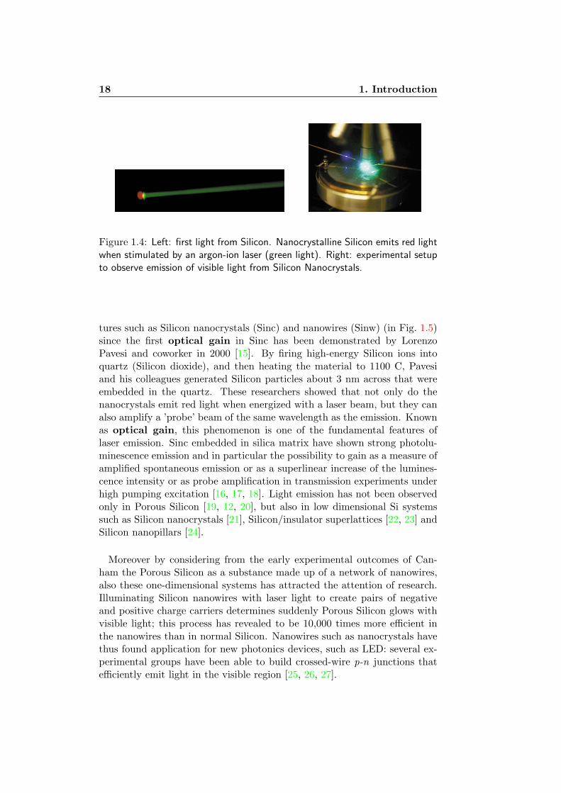
Furthermore one of the main point of attraction on Silicon photonicslies in the possibility to achieve not only light from Silicon-based devices,but prominently to achieve gain of light from this dispositive, as shown inFig. 1.4. In particular great attention has been payed to Silicon nanostruc-
18 1. Introduction
Figure 1.4: Left: first light from Silicon. Nanocrystalline Silicon emits red lightwhen stimulated by an argon-ion laser (green light). Right: experimental setupto observe emission of visible light from Silicon Nanocrystals.
tures such as Silicon nanocrystals (Sinc) and nanowires (Sinw) (in Fig. 1.5)since the first optical gain in Sinc has been demonstrated by LorenzoPavesi and coworker in 2000 [15]. By firing high-energy Silicon ions intoquartz (Silicon dioxide), and then heating the material to 1100 C, Pavesiand his colleagues generated Silicon particles about 3 nm across that wereembedded in the quartz. These researchers showed that not only do thenanocrystals emit red light when energized with a laser beam, but they canalso amplify a ’probe’ beam of the same wavelength as the emission. Knownas optical gain, this phenomenon is one of the fundamental features oflaser emission. Sinc embedded in silica matrix have shown strong photolu-minescence emission and in particular the possibility to gain as a measure ofamplified spontaneous emission or as a superlinear increase of the lumines-cence intensity or as probe amplification in transmission experiments underhigh pumping excitation [16, 17, 18]. Light emission has not been observedonly in Porous Silicon [19, 12, 20], but also in low dimensional Si systemssuch as Silicon nanocrystals [21], Silicon/insulator superlattices [22, 23] andSilicon nanopillars [24].
Moreover by considering from the early experimental outcomes of Can-ham the Porous Silicon as a substance made up of a network of nanowires,also these one-dimensional systems has attracted the attention of research.Illuminating Silicon nanowires with laser light to create pairs of negativeand positive charge carriers determines suddenly Porous Silicon glows withvisible light; this process has revealed to be 10,000 times more efficient inthe nanowires than in normal Silicon. Nanowires such as nanocrystals havethus found application for new photonics devices, such as LED: several ex-perimental groups have been able to build crossed-wire p-n junctions thatefficiently emit light in the visible region [25, 26, 27].

Doping goes to nano 19
Figure 1.5: Top: TEM image of Silicon nanocrystals embedded in an oxidematrix. Bottom: TEM and SEM images of bunch of Silicon nanowiress.
1.3 Doping goes to nano
Although the great effort in the research for a Si based emitting light sourceand even if it has been found that Si nanocrystals band-gap increases withdecreasing size with a luminescence external efficiency in excess of 23%,Si nanocrystals (Sinc) still have a memory of the indirect band gap ofthe bulk phase and this is evidenced by the clearly observed structuresrelated to momentum-conserving phonons [28, 29]. Although in Siliconnanocrystals the quantum confinement breaks the k-vector selection ruleand allows direct radiative transitions even without phonon assistance,the calculated radiative lifetime remains long, more than 10 µs, for Sinc

20 1. Introduction
containing more than 20 atoms as confirmed by theoretical [30] andexperimental [31] evidence. Since the Auger lifetimes τ lie between 10−1
and 102 nanoseconds (ns), these non radiative recombination process aremuch faster and more competitive than the radiative ones. This drawbackcan be circumvented by doping Silicon nanostructures, thus by introducingisoelectronic [32] or n- and p- type impurities [29, 12, 33] within both na-nocrystals and nanowires in order to sustain more the radiative transitionsand diminish the competitive quenching action of the Auger decay processes.
Yet impurities play a central role in semiconductor technology. Perfor-mance of a semiconductor device is dictated by shallow dopants. Shallowdopants like Boron (B) and Phosphorus (P) alter the conductivity of bulkSilicon by several orders of magnitude. Deep defects, on the other hand,are known to degrade device performance. These properties are expected tobe significantly altered in highly confined systems such as Sinc. Importantquestions arise as to whether dopants will continue to play a role similar tothat in bulk semiconductors and whether new applications will become pos-sible. Experimental studies of impurities in Sinc have been slow to addresssuch issues, the major part due to difficulties in preparation of samples in acontrollable manner. To date, efforts have focused almost exclusively on: (i)studies of Boron-doped or Phosphorus-doped Si nanowires [34, 35], materialsthat have enabled the assembly and fabrication of field-effect transistors andbiosensors, and (ii) the possible control of the photoluminescence propertiesof Si nanodots by n- and p-type impurities [36, 37]. Concerning these exper-iments several questions are still open: in some cases a very low conductivityis measured, thus it is not clear whether or not the doping of Sinc providesa generation of free charge carriers. In the case of Si nanowires a decreasein mobility with decreasing dopant concentration has been observed thatcontrasts the usual behaviour in bulk Si, where increase in dopant concen-tration leads to increased scattering and a reduction in mobility; it is notclear if this effect is intrinsic or not to the one-dimensional geometry of thewires.
In the last years the experimental group of Minoru Fujii has demonstratedthat the simultaneously insertion of n- and p- type impurities, such as Boronand Phosphorus, within the Silicon nanocrystals tends to suppress the PLquenching that normally arise in undoped Sinc or when stand-alone donor oracceptor impurity are individually present [36, 37, 38]. It has been demon-strated infact by Kovalev and coworkers [39] that, when single donor oracceptor impurities are present within the nanocrystals, due to the spatiallocalization of excitons in the vicinity of neutral impurities the effective con-centration of the carriers (two photogenerated + one intrinsic) is very highon the order of 1018 to 1019 cm−3: at these concentrations the most effectiverecombination mechanism in Si is the Auger process. Thus the crystallites

Doping goes to nano 21
Figure 1.6: Annealing temperature dependence of (a) pure nc-Si, (b) B-dopednc-Si (left side) and (c) P-doped nc-Si, and (d) B- and P-codoped nc-Si (rightside). All spectra are taken at the same condition. The vertical red line is drawnat the band-gap energy of bulk Si crystals s1.12 eV.
containing a single shallow impurity are ”dark” [33, 40, 41].
By simultaneously doping Silicon nanocrystals instead, Fujii demonstratethat PL properties of P and B codoped Sinc’s assemblies have the PL maxi-mum below the band-gap energy of bulk Si crystals and also that the mech-anism of the PL is different from that of pure Sinc’s. Under resonant PLexcitation condition, impurity codoped samples exhibit quite different PLspectra from those of pure Sinc’s.
In particular B and P codoping suppress the quenching of photolumines-cence that occurs when only Boron or Phosphorus are singularly present;furthermore the codoped nc exhibit stronger PL peaks shifted to lowerenergies with respect to the corresponding undoped and single doped Sincand in particular below the bulk Silicon band gap limit as in Fig. 1.6, thusdemonstrating that by simultaneously doping n- and p- type impurities inSinc, it’ s possible to change the indirect band-gap nature of pure Sinc todirect ones without losing the intensity as shown in panel (d) of Fig. 1.6.This approach may further improve the luminescence efficiency of Sinc aswell as extend the tunable range of the luminescence energy. However, to

22 1. Introduction
make the benefit of this effect maximum, carriers in all nanocrystals in asample should be compensated.
Since impurity doping is expected to change significantly the electronicband structure of nanocrystals, there is a need of a detailed theoreticalknowledge of their electronic states, crucial to fully understand their opti-cal and electrical transport properties. Theoretical studies of impurities inquantum dots and wires have lagged relative to calculations for pure, un-doped systems. To the best of our knowledge only few theoretical studiesexist in literature related to the role of doping on Silicon nanostructuresand, for what concern the nanowires, mostly of them are mainly focusedon the electronic conductance and transport properties of n- or p- type sin-gle doped nanowires and based on semi-empirical tight binding approach[42]. Impurity surface segregation strongly affects the conductance with re-spect to the undoped Sinw. Boron or phosphorus single doping leads tosignificantly different conductance properties in wires compared to bulk; inparticular, single P- doped wires subdue to a drop of conductance due toa strong resonant backscattering that reduces the mobility of carriers atselected energies.
The idea of this thesis comes form the fact that very few and/or not con-clusive theoretical studies exist on the role played by single and co- dopingon the optical properties of Sinc and in particular on Sinw [43]. In particularour aim is to focus the attention on the role played by simultaneous substi-tutional impurities like Boron and Phosphorus on the electronic and opticalproperties of these nanostructured systems, finding out what does also re-ally change in the electronic structures and in the optical response whenwe move from 3D confined nanodots to 2D confined nanowires by a firstprinciple calculations. Absorption and emission spectra will be calculatedwithin a Many-Body approach by means of the GW self energy correctionsand excitonic effects in order to bring out the most reliable study to shedmore light on the possibility to engineer and tune the emission of light fromcodoped Silicon nanostructures.
1.4 Physical Properties of undoped SiNC
Silicon nanocrystals are quasi 0- dimensional nanosized system that can besynthesized in different ways. Deposition techniques from silane decomposi-tion in gas phase or from laser ablation permit to obtain Sinc with accuratesize and concentrations. Other techniques such as the chemical vapor depo-sition (CVD) or the ion implantation produce Sinc embedded in an Oxidematrix compatible with integrated circuits (IC) applications. They havecrystalline structure that preserve most of the symmetry properties of theinfinite bulk crystal, and can be treated as spherical [44] or facetted [45] nc.

Physical Properties of undoped SiNC 23
• due to the quantum confinement they have quasi-direct energy gapwith discrete quantized energy level with respect the indirect be-haviour of bulk Silicon; the energy gap can be considered direct atthe Γ k-point due to the band folding; it decreases with the increas-ing of the nc diameter approaching to the bulk limit value as the sizeaugment.
• the Sinc present a breakdown of the k-conservation rule: the spatialconfinement of electrons and holes increases the uncertainty of theircrystal momentum thus allowing optical transition which don’t requirethe mediation of phonons as instead happen in indirect band gap semi-conductor.
• Sinc are able to emit light after being excited with optical laser. Inparticular this photoluminescence emission of light (PL) is enhancedwhen dealing with Sinc ranging from 1 to 5 nm of diameter (dispersionin size). From several experimental works, it comes out that Sincare characterized by a Stokes shift between absorption and emissionprocesses. This phenomenon could be related to the relaxation thatthe nanocrystals subdue after the optical excitation process. Thisamount of difference between the absorption and emission energiesis a decreasing function of the nc diameter: it’s bigger for smallernanocrystals, while it tends to be negligible when the size increasetoward the bulk limit.
• several theoretical works have been realized in the last decade con-cerning the simulation of isolated-free standing hydrogenated Si na-nocrystals [44, 46, 47, 48, 45, 49, 50, 51]. Through different approach(DFT-LDA, Time Dependent DFT, Quantum Montecarlo, Real Spaceapproach) these nanocrystals have been studied in order to understandand reproduce the electronic and optical features of Porous Siliconwhich has been demonstrated to be constituted, as prepared, by a ro-bust network of interconnected Si nanostructures that move from thenanowires to the nanocrystals size as the porosity increases. Moreover,after the demonstration that light emission can be achieved both fromaged Porous Silicon samples and from Si nanocrystals embedded in anoxide (SiO2) matrix [52, 15], several work has been realized in orderto bring out which role plays the oxygen at the surface on the opticalfeatures [53, 20, 54, 55, 56, 57, 45] by comparing theoretical resultswith the experimental outcomes. In particular, among the numerouscalculations done, the more sophisticated tend to go beyond the simpleDFT-LDA approach related to total energy calculation of the GroundState but aspire to shed some more lights on the study of the ExcitedState, by taking explicitly into account the electron-hole interactionthrough different kind of approach, such as Green function approach,

24 1. Introduction
Constrain DFT scheme or Time Dependent DFT.
1.5 Physical Properties of undoped SiNW
Silicon nanowires are quasi one-dimensional systems. As for Silicon na-nocrystals several growth techniques exist, and for each of them differentapplications can be realized. The most common fabrication technique isthe Vapor-Solid-Liquid (VSL) growth, in which a metal particle is used tocatalyze the growth reaction of the nanowires. The main effects of low di-mensionality are:
• size scaling of the optical gap. The effect of uni-dimensional spatialconfinement of carriers along the two direction perpendicular to thewire axis determines that electrons holes are free to move all along thewire axis. This determines an opening of the band gap which variesas a function of the wire diameter. The optical properties instead,don’t depend so much on the wire diameter, but indeed on the wireorientation. This anisotropic behaviour could help in the identificationof the different wires grown in a sample.
• as already said for Silicon nanocrystals, the Silicon nanowires presenta direct optical gap, due to the band folding of the energy bands onthe axis of the nanowires.
• Sinw show strong electron-hole interaction effects when compared tothe bulk compounds. As before, the spatial confinement of the carriersalong the wire axis, determines a strong overlap of their wavefunctionsthat results in an increasing of the interaction effects. It has been foundthat strong bounded exciton present a binding energy 103 times biggerwith respect to the corresponding value in bulk Silicon.

2Density Functional Theory
Queremos la luz, para nosotros nadaqueremos la luz, para todos todo.
La lunga notte, Cisco
Since this work concerns of theoretical simulations of real (or that pretendto be almost real!) systems for ponderable technological application, weadopt the most used and efficient technique to deal with success in thiskind of study. To understand the electronic ground-state properties of thesystems we have taken benefit of ab initio approach based on the densityfunctional theory (DFT) scheme. But, although the well known and testedefficiency of DFT, we had to recourse to the Many-Body PerturbationTheory (MBPT) to treat in the proper way the excited-state features, thatmeans charged and neutral excitations, such as optical absorption andemission.
Thus this section will pursue with a brief description of some important and,of course, well known features of DFT and MBPT scheme implemented inthe ab initio computer codes used in the present work to investigate oursystems of interest.
2.1 The Many-Body Problem
One of the principal aim of condensed matter physics and quantum chem-istry is the theoretical study of the electronic properties. To understandthe behaviour of systems ranging from atoms, molecules and nanostructuresto more complex bulk systems, the resolution of the Schrodinger equationhas become the fundamental and the main task of the many-body prob-lem. Since the Coulomb or electrostatic interaction between electrons is
25

26 2. Density Functional Theory
very strong, the analytical solution of this equation is possible only for asmall number of very simple systems and in particular numerical solutionscould be found only for a few number of atoms and molecules. The mainand computational demanding problem lies in the many-body nature of theHamiltonian H that governs the evolution of any systems composed by elec-trons (labelled by coordinates (position and spin) ri, momenta pi, massmi) and atomic nuclei (represented by coordinates RI and momenta PI
with mass MI and atomic charge ZI):
H[r,p R,P
]=
N∑
i=1
pi2
2mi+
M∑
i=1
PI2
2MI+
∑
I<J
e2
|ri − rj|+
−∑
i<j
ZI e2
|ri − RI|+
∑
I<J
ZI ZJ e2
|RI − Rj|
and that is also applied to the many-body wavefunctions
ΨMB = (r1, ..., rn ; R1...,RN)
describing the eigenstates of the complex real system, in terms of electronsand atoms contributions through a many-body secular equation
H(ri, RI
)ΨMB
(ri, RI
)= Etot ΨMB
(ri, RI
)(2.1)
Due to the huge number of interactions involved this problem is enor-mously complex to resolve and also nowadays very tough also for the mostpowerful supercomputer. Thus the physics and chemistry community hasbeen obliged to find some approximation that worked to simplify the task.The first one, exploited by M. Born and M. J. Oppenheimer during 1927,introduces a hierarchy of approximation due to different scales of energy.The so called Born-Oppenheimer or adiabatic approximation [58] tends infact to decouple the nuclear and the electronic degrees of freedom. Sinceelectrons move much faster than nuclei it can be assumed that electronsare in the lowest energy state for the given nuclear configuration: electronsand nuclei moves on different energy and time scale so that electrons followadiabatically the slow ”motion” of nuclei.
Thus, according to the Born-Oppenheimer Approximation, we can separatethe electronic variable from the nuclei ones factorizing the many-body wave-function into two contributes:
ΨMB ⋍ ΨBO = ϕ(r, R) Φ(R) (2.2)
Then the secular eigenvalues equation Eq. [2.1]
(Te + TI + Vee + VIe + VII ) ΨMB(ri, RI) = Etot ΨMB(ri, RI)

The Many-Body Problem 27
(where the sum terms have been replaced by T for the kinetic energy andV for the potential energy) can be separated into two coupled equations
[Te + Vee + VIe
]ϕ(r, R) = E (R) ϕ(r, R)[
TI + VII + C (R)]
Φ(R) = Etot Φ(R) (2.3)
This means that now the properties of electrons depend on the nucleicoordinates RI in a parametric way: since the nuclei (or ions) aresupposed to be frozen we can see that the ionic potential enter as aparameter in the equation for electrons Eq. [2.3] and the electrons inthe ionic counterpart equation via the adiabatic parametric energy termC (R), which represents a sort of electronic glue for the lattice. Note thatthe energy term CR, called adiabatic diagonal correction, is an operatorthat acts on the nuclear wave function Φ(R) and is generally quite smalland is mostly neglected altogether.Once the electron equation has been separated by the ionic counterpart,there’s still another open question blinking on the paper: how to resolvethe electron eigenvalues equation from the quantum theory point since itdescribes (with the Vee) interactions between 1023 electrons per materialand the index of the wavefunction ϕ(r, R) runs over N -electrons?We have again to deal with a ”many-body Schrodinger equation”!
Several models have been proposed during the last century to treat in asimply but proper way this new formidable ”many-body task” of interactingelectrons. Most of this approximate theories concerns with finding a goodsingle-particle approximation for the Coulomb term.The earliest attempt is due to D. R. Hartree in 1928 [59]. The main featuresof the Hartree approximation are:
• the non local Coulomb potential is replaced by a local Coulomb poten-tial (Hartree potential) averaged by all the electrons of the systems
VH =
j=1∑
N
∫d3r′ ϕ∗
j (r′)ϕj(r
′)1
| r − r′ | =
∫d3r′ ρ(r′)
1
| r − r′ |(2.4)
• the many-body electron wavefunction ϕ(r, R) is separated intoa product of N single-particle function satisfying a one-electronSchrodinger equation.
ϕ(r, R) ⋍ ϕH = ϕi(r1) ϕi(r2) ϕi(r3) ... ϕi(rj) (2.5)
Although the Hartree approximation gives reasonable results, it miss theeffect of exchange and correlation between electrons (that are partially
28 2. Density Functional Theory
cancelled each other) and also doesn’t take into account the Pauli exclusionprinciple, so neglecting the spin component effect.
Taking into account Fermi-Dirac statistic the wavefunction can be describeas a Slater’s determinant of single-particle wavefunction, in order to treatthe wavefunction as anti-symmetric with respect to any interchange of twoelectrons,
ϕ(r, R) ⋍ ϕHF =1√N !
det [ϕi (rj) ]
it’s possible to go beyond the Hartree potential obtaining the so calledHartree-Fock method where an additional non local spin-dependent ex-change term appears in the Hamiltonian [60]:
∫d3r′ Vx(r, r
′) ϕi(r′) = −
Noccup∑
j=1
∫d3r′ ϕ∗
j (r′)
1
| r − r′ | ϕj(r)ϕi(r′) (2.6)
In this new approach the exchange contribution Vx is now treated ex-actly and improves the total energy predictions for atoms and moleculesalthough fails describe solid state systems, such as insulators for whichthe energy gap is overestimated. What the Hartree-Fock methods missis the correlation between electrons with different spin and therefore thescreening. One possibility to go beyond Hartree-Fock approximation is donein the configuration interaction (CI) scheme [61]. In this method a set ofSlater determinants is considered as a basis for many-body wavefunction,but the number of configurations scales very rapidly with the number ofelectrons making the method extremely demanding (linear combination ofthe determinants are considered to describe the lowest-lying state, but theincreasing number of configurations with increasing number of electronsmeans that only systems with a few number of electrons can be calculatedwith high accuracy).All these method belong to the class of mean field approximation: allthe electrons experience an ”averaged” potential due to the electrostaticinteraction with the charge density formed by all other electrons in thesystems.
A different approach was adopted by Thomas and Fermi (1927-1928) [62, 63]who proposed to cast the many-body problem into a semiclassical variationalframework in which the degrees of freedom of the systems were condensedinto the electron density n(r) only. Extensions of this method were suggestedby Dirac (1930) [64] introducing the exchange interaction between electronsas a functional of the density, and by Slater who introduced correlationseffects. These were the basis for the development of the Density FunctionalTheory.

Another brick in the wall: a brief DFT survey 29
2.2 Another brick in the wall: a brief DFT survey
Although in the Thomas-Fermi model is possible to introduce correction(such as exchange and correlations effects or gradient density with the ex-tension of Dirac) that can lead to really good results, it can’t be consideredthat a first simpler version of the density functional theory. The first the-oretical foundation of Density Functional Theory (DFT for friends!) wasintroduced in 1964 by P. Hohenberg and W. Kohn in a famous paper [65]that was worth the Nobel Prize for Chemistry to Kohn in the 1998. Theydemonstrated that all the electronic properties of the system in its non-degenerate ground-state (GS) configuration can be completely describedby its electron density n(r); moreover the total energy and the potentialscan be described as functional of the electron density n(r) only.One year later, in 1965, moving from the H-K theorem, W. Kohn and L.J. Sham provided a self-consistent scheme in order to map the interactingmany-body problem into a set of non interacting single particle equation re-formulating the mean-field method into a variational principle on the basisof the electron density only [66]. The first milestones of Density Func-tional Theory can therefore considered the Hohenberg-Kohn theorem andthe Kohn-Sham equations.
The Hohenberg-Kohn theorem
The Hohenberg-Kohn (H-K) theorem succeeded to demonstrate that theproperties linked to the electronic structure of a system in its fundamentalnon-degenerate ground-state are completely and univocally described by itselectronic ground-state density n(r). The theorem asserts that:
”the ground-state density n(r) of a bound system of interacting electrons insome external potential v(r) determines this potential uniquely”
where uniquely means ”up to an additive constant” (defined in theHohenberg-Kohn paper, uninteresting) and in the case of degenerate ground-state, the lemma refers to any ground-state density n(r). Taking into ac-count a N-electron system interacting in presence of an external potentialVext(r), the Hamiltonian results
H = T + Vext + W
a sum of a kinetic term
T = − 1
2
N∑
i
∇2i
an electron-electron interaction Coulomb potential term
W =1
2
∑
i6=j
vij ( |ri − rj | )

30 2. Density Functional Theory
and a term representing the interaction with the external potential Vext(r)
Vext =N∑
i
vext (ri)
the ground-state many-body wavefunction can be defined as ϕ(r1. . . ϕN )and the ground-state electronic density (supposed to be non-degenerate) is
n(r1) = N
∫ϕ∗(r1. . . ϕN ) ϕ(r1. . . ϕN ) dr2. . . drN
The H-K theorem asserts that ϕ and Vext1 are univocally determined by
the electronic density n(r) only and they’re called unique functional of theelectronic charge density. From the eigenvalues equation
H |ϕ(r) 〉 = EGS |ϕ(r) 〉(T + V + W
)|ϕ(r) 〉 = EGS |ϕ(r) 〉 (2.7)
although T and W are univocally specified through the H-K theorem, on theother hand, the potential v, supposed in the original paper [65] to be local,bounded and spin-independent, can be considered an element of the V en-semble containing all the external potential that generate a non-degenerateground-state for the system. Each v can be related to a ground-state wave-function ϕGS to which belong a unique electronic charge density nGS(r):
nGS(r) = 〈ϕGS | n(r) |ϕGS 〉
All the densities that satisfy this relation belong to the ensemble N andare called v-representable because are ground-state electronic densities of thehamiltonian H = T+W+V obtained from different vext =
∫v(r)n(r) dr ∈
V . It’s possible to construct a map between a set of external potential v(r)and the corresponding ground-state densities n(r) through:
G : v(r) → |ϕ(r) 〉
and since the H-K theorem shows that G is surjective and injective, thusbiunivocal and fully invertible:
G−1 : n(r) → v(r) + c
the ground-state density could be considered the basic variable in the elec-tronic problem. The application G is surjective for construction but to provethat is also injective one can shows that two different systems subjected totwo external potentials that differ only for a constant, v(r) 6= v′(r)+ c they
1From now on the external potential will be simply indicated by v

Another brick in the wall: a brief DFT survey 31
cannot have the same electronic density for the ground-state, n(r) = n′(r)leads to an absurdum.This implies that the ground-state expectation value of any physical observ-able is a unique functional of the ground-state electron density n(r):
〈ϕ[n]| O |ϕ[n] 〉 = O[n]
In particular according to these findings we can define the total energy of theN -electron system as the expectation value calculated on the ground-statewavefunction |ϕ〉:
E[n(r)] =⟨ϕ[n]
∣∣ H∣∣ϕ[n]
⟩
and defining the universal functional FHK [n]:
FHK [n] =⟨ϕ[n]
∣∣ (T + W )∣∣ϕ[n]
⟩(2.8)
the total energy become:
Ev[n(r)] =
∫v(r)n(r) d r + FHK [n] (2.9)
It is worth pointing out that FHK [n] is a universal functional because itdoesn’t depend on the external potential and it is the same density functionalfor atoms, molecules and solids since in all cases W is the Coulomb repulsionbetween the electrons and T their kinetic energy.The second part of the H-K theorem establish that through a reformulationof the Rayleigh-Ritz variational principle in term of the electron densityn(r) is possible to minimize the Ev[n] functional in the class of the regularfunctions n(r) satisfying the condition
∫n(r) d r = N for the exact ground-
state density [67]. The minimization process leads to
E = minn(r)Ev[n] = minn(r)
∫v(r)n(r)dr + F [n]
(2.10)
where here n(r) refers to all functions of the v − representable class citedabove. The minimum is attained when n(r) coincides with the n(r) ground-state density for a non-degenerate case; for a degenerate case, instead, n(r)is only one of the ground-state densities. The constraint on the number ofparticles (that assures the conservation) is resumed with
δE[n(r)]
δn(r)= µ. (2.11)
where µ mathematically defined as a Lagrange multiplier represents thechemical potential of the system.The formidable problem of finding the minimum of 〈Ψ | H | Ψ〉 with respectto the 3N− dimensional trial function Ψ has been transformed into the
32 2. Density Functional Theory
seemingly trivial problem of finding the minimum of Ev[n] with respect tothe three-dimensional trial function n(r). However the main difficulty inthe determination of the ground-state density is the form of the functionalEq. [2.8]: fixed the external potential vext(r) the lack of a proper analyticaldefinition of the FHK [n] functional leads straight the use of approximationsfor the minimization of Ev[n(r)] for the calculation of Etot and n(r).
The Kohn-Sham equations
A particulary important strategy to solve the problem of the practical DFTimplementations was introduced by Kohn and Sham [66].They considered an auxiliary system of N non-interacting electrons sub-jected to an effective potential vKS
eff (r) and described by the Hamiltonian:
HKS = TKS + vKSeff . (2.12)
by moving from the initial Hartree formulation of the Schrodinger equationfor noninteracting electrons in the external potential veff and from the H-Kminimal principle. According to the theorem of Hohenberg and Kohn, for anon-interacting N -particle system, the energy is a functional of the density:
Es[n] = Ts[n] +
∫vs(r)n(r)dr (2.13)
The central assertion used in establishing the Kohn-Sham scheme is thefollowing: ’ ’for any interacting system, there exists a local singleparticle potential vks(r) such that the exact ground-state densityn(r) of the interacting systems is equal to the ground-state densityof the auxiliary system n(r), i.e. that n(r) = n(r)”.
We limit our discussion to non degenerate systems, for a more generalapproach see [67].Minimizing the energy functional for the Kohn-Sham system of N -independent particles, with the constrain on the number of electrons andconsidering that the density n(r) must be constructed for an independent-particle system (one-single Slater determinant), we obtain a set of equations:
[− ~
2
2m∇2 + vs(r)
]ϕi(r) = ǫiϕi(r) (2.14)
The density has a unique representation in term of the (lowest) N single-particle orbitals:
n(r) = n(r) =N∑
i=1
| ϕi(r) |2 (2.15)

Another brick in the wall: a brief DFT survey 33
where the constraint on the density became equivalent to the orthonormalityof the wavefunctions: ∫
drϕ∗j (r)ϕi(r) = δij (2.16)
Once the existence of a potential vs(r) generating a given interacting densityn(r) is assumed, the uniqueness of vs(r) follows from the Hohenberg-Kohntheorem.Thus the single-particle orbitals are unique functional of the density: n(r),φi(r) = φi([n(r)]) and the non interacting kinetic energy Ts[n(r)] is aunique functional of n(r) as well.
Starting from the interacting system subject to an external potential v(r)we can rewrite the total energy functional of Eq. [2.9] splitting FHK [n] as:
FHK [n] =1
2
∫ ∫drdr′
n(r)n(r′)
|r − r′| + Ts[n] + Exc[n] (2.17)
and obtaining in this way:
Ev[n] = Ts[n] +
∫dr v(r)n(r) +
1
2
∫ ∫dr dr′
n(r)n(r′)
|r − r′| + Exc[n] (2.18)
where we have inserted three terms in FHK [n] such as:
• the Hartree energy term 12
∫ ∫drdr′ n(r)n(r′)
|r−r′| describing interaction be-tween electrons
• the kinetic energy Ts of the non-interacting system
• the term Exc[n] called exchange-correlation energy and unfortu-nately still unknown, defined as
Exc[n] = FHK [n] − 1
2
∫ ∫drdr′
n(r)n(r′)
|r − r′| − Ts[n] (2.19)
but from Eq. [2.8] we can see that Exc consists of a potential and akinetic part:
Exc[n] =
(W [n]− 1
2
∫ ∫drdr′
n(r)n(r′)
|r − r′|
)+
(T [n]+Ts[n]
)(2.20)
The Hohenberg and Kohn variational principle ensures that Ev[n] is sta-tionary for small variations of δn(r) around the minimum density n(r):
δEv[n] = E[n+ δn] − E[n] = 0

34 2. Density Functional Theory
∫δn(r)
v(r) +
δ Ts[n]
δn(r)+
1
2
∫n(r)
| r − r′ |dr′ +
δ Exc[n]
δn(r)− µ
n≡n
dr = 0
(2.21)
Applying the Euler-Lagrange equations
δTs[n(r)]
δn(r)+ v(r) +
1
2
∫n(r′)
|r − r′|dr′ +
δ Exc[n(r)]
δn− µ = 0 (2.22)
introducing an exchange-correlation potential vxc defined as:
vxc(r) =δExc[n]
δn(r).
and an effective potential
vKSeff (r) = v(r) +
1
2
∫n(r′)
|r − r′|dr′ + vxc(r)
one can finally get the so called self-consistent Kohn-Sham (KS) equa-tions [66]:
− 1
2∇2 + vKS
eff (r) − εKSi
ϕKS
i = 0 (2.23)
where the εKSi and ϕKS
i are the Kohn-Sham respectively eigenvalues andeigenvectors. It can be observed that since
N∑
i
εi =∑
i
〈ϕi | −1
2∇2 + veff (r) | ϕi〉 =
= Ts[n(r)] +
∫veff n(r)dr =
= Ts +
∫v(r)n(r) dr +
1
2
∫n(r)n(r′)
|r − r′| drdr′ +
+
∫vxc(r)n(r)dr (2.24)
and
Ev[n] = Ts +
∫v(r)n(r)dr +
1
2
∫n(r)n(r′)
| r − r′ | drdr′ + Exc[n]
then the total energy of the interacting system can be expressed in this way:
Etot = Ts[n] +
∫vext(r)n(r) d r +
1
2
∫n(r)n(r′)
|r − r′| drdr′ + Exc[n] =
N∑
i
εi −1
2
∫n(r)n(r′)
|r − r′| drdr′ + Exc[n] −
∫vxc(r)n(r) d r (2.25)

Another brick in the wall: a brief DFT survey 35
If one neglects the Exc and the vxc terms altogether, the KS equations(2.2, 2.23, 2.25) reduce to the self-consistent Hartree equations. The samemust holds also for the non-interacting systems and we can write:
0 = δEs[n] = Es[n+ δn] − Es[n] = δTs +
∫dr δn(r)vKS(r) (2.26)
This leads to the final expression as seen above:
vKSeff (r) = vext(r) +
∫dr′
n(r′)
|r − r′| + vxc(r) (2.27)
The Kohn-Sham formalism relies on the link between an actual N electronssystem and a fictitious non-interacting counterpart through the potentialvxc(r). Hence, vxc(r) contains essential information about many-body cor-relations which Many-Body Perturbation Theory describes [68, 69] in termsof non local dynamical terms.
It may be realized that the mapping between ground-state densities andKohn-Sham potentials vKS [n](r) depends on n(r) in a very peculiar andsensitive way. In fact the actual functional relation between n(r) and vxc(r)is highly non-analytical: small or even infinitesimal changes in the densitymay induce substantial variations in the xc potential. It is highly nonlocal, i.e. changes in the density at a given point r may induce substantialvariations of the xc potential at a point r′.
The KS equation can be regarded as the exact formalization of the Hartreescheme: with the exact Exc and vxc all the many-body effects are completelytaken into account by principle, and the main effort of DFT lies in thepractical usefulness of ground-state when the good approximation (simplyto use but accurate) for the xc functional is found.

36 2. Density Functional Theory
Some remarks:
1. the Hartree potential gives an exact estimation of the exchange poten-tial but tends to neglect the correlation effects between electrons of thesystem: for that reason the Hartree equations tend to underestimatethe total energy;
2. the KS equation, instead, take into account both the effects of exchangeand correlation contained in the Exc[n] functional;
3. the effective single-particle potential Veff can be regarded as a uniqueexternal potential which leads for noninteracting particles, to the samedensity n(r) as that for the interacting electrons in the physical exter-nal potential v(r);
4. the initial N -electron many-body problem (very computational de-manding) is simplified to a set of n single-particle equations describinga fictitious system of noninteracting electrons with electron density ofthe real system of interacting electrons;
5. the single-particle KS wavefunction ϕKSi (r) are considered ”density
optimal” while the Hartree-Fock wavefunction ϕHFj are ”total energy
optimal” because their normalized determinant leads to the lowestground-state energy attainable with a single determinant
Within the Kohn-Sham scheme the problem of the interacting system isnow simpler, but it is still not solved: it is necessary, in fact, to find a goodapproximation for the exchange-correlation energy Exc.Once a good approximation for Exc is obtained, the Kohn-Sham equationsmust be solved self-consistently and then it is possible to obtain the ground-state density of the interacting system and its total energy, as depicted inFig. 2.1.
2.2.1 The form of Exc
Since there’s no exist an exact analytical expression for the Exc functional,the total energy calculations require some approximations for it. In the nextsection I’ll fix the attention on three of these approximations that are used inthis work: the Local Density Approximation (LDA), the Local Spin DensityApproximation and the Generalized Gradient Approximation.
The Local Density Approximation
According to this approximation, disclose to be the simplest and most usedone, the xc functional is defined as a local function of the density of a

Another brick in the wall: a brief DFT survey 37
Figure 2.1: The main Self-Consistent Algorithm
homogeneous electron gas:
Exc =
∫dr ǫhom
xc
(n(r)
)
where ǫhomxc is the exchange-correlation energy per electron of the homoge-
nous and uniform electron gas. Taking into account an interacting homo-geneous electron gas, we can say that the exchange-correlation energy perelectron is in this case a function of the density and not a functional sincethe density is constant for this kind of system: thus ǫxc[n(r)] → ǫxc(n(r))and multiplying for the number of electron we get Exc[n] = Nǫxc(n(r)). Inthe Local Density approximation, the inhomogeneous electron gas is handledin the same way: the exchange-correlation energy is the sum of the contri-bution of each portion of the non uniform gas as it was local uniform.Thus the exchange-correlation potential become:
vLDAxc (r) =
∂Exc[n]
∂n(r)=∂
∫ǫxc(nr)n(r)dr
∂n(r)=
∂[n(r)ǫxc(r)]
∂n(r)= ǫxc(nr) + n(r)
(∂ǫxc(n)
∂n
)
n(r)
≡ µxc(n(r)) (2.28)
where µxc(n(r)) is the exchange-correlation contribution to the chemicalpotential for an uniform system. The approximation is said to be local be-

38 2. Density Functional Theory
cause ǫxc(r) depends from the local value of the density n(r) in the r positiononly. The LDA works well for systems with a slowly varying density and hasproven very successful for calculation of ground-state properties. The lat-tice constants are predicted within ∼ 1 %, the bulk modulus, the dissociationenergy of molecules, the ionization energy of atoms within ∼ 10 % of experi-ment, while the cohesive energy is quite generally overestimated, as a resultusually attributed to the predicted under bindings of atoms within LDA. Onthe other hand the LDA fails in the estimation of the fundamental energygap for semiconductors and insulator, usually underestimated by 30 - 50 %,although the relative position of the valence band energies for bulk materialsagree well with photoemission experiments [70]. The two contributions toExc, the exchange and the correlation energy respectively within ∼10 % and2 times bigger, tends to compensate and cancel. Thanks to Eq. [2.28] theEtot of Eq. [2.25] can be expressed in this way:
Etot =N∑
i
εi −1
2
∫n(r)n(r′)
|r − r′| drdr′ +
∫n(r)
[ǫxc(n(r)) − µxc(n(r))
]d r
(2.29)where the contribution ǫxc can be exactly derived taking into account thewavefunction of the homogeneous electron gas as a Slater determinant ofplane waves:
ǫxc(nr) =
[3
4
(3
π
)1/3
e2
]n(r)1/3 = −0.458
rse2
where e2 is the radius of the sphere containing one electron given by(4π/3)r3s = n−1. The correlation term, derived by Wigner in 1938,
ǫxc(nr) = − 0.44
rs + 7.8
was corrected with better precision by David Ceperley and Ben Alder in1980 [71] through Monte Carlo methods.
As remarked above, the LDA is expected to be useful only for densityvarying slowly on the scales of the local Fermi wavelength λF and Thomas -Fermi wavelength λTF and, nevertheless, it gives good results for atoms andmolecules. The reason lies in the fact that LDA satisfies a sum rule whichexpresses the normalization of the exchange-correlation hole. This meansthat with an electron in r, the conditional electron density n(r, r′) of theother electrons is depleted near r in comparison with the average densityn(r′) by the hole distribution nh(r′; r) which integrates to 1. The success ofLDA lies then in
• the exchange-correlation energy is well determined by the sphericalaverage of the exchange-correlation hole;

Another brick in the wall: a brief DFT survey 39
• the Local Density Approximation describes with accuracy this kind ofspherical average;
• there’s a systematic cancellation between the errors as a consequenceof the charge conservation in the sum rule;
LDA energy functional suffers for the self-energy interaction: the exchangepart of the functional does not cancel exactly the self-energy interaction ofthe Hartree term. This leads to a wrong asymptotic behaviour of the xcpotential for finite systems (it goes exponentially to zero instead as 1
r ) [72].There have been several attempts to go beyond the LDA approximation[73]: the next class of functionals, in which we can consider the GGA[74], solve some of the problem present in the LDA, but they are justanalytical semi-local approaches. The novel meta-GGA include furthernon-analytical and non local behaviour through the explicitly appearanceof the Kohn-Sham wavefunctions, but both GGA and meta-GGA have thewrong asymptotic behaviour.Another class of energy functionals are the orbital functionals, in the socalled optimized effective potential (OEP), or optimized potential method(OPM) [75, 76, 77]. Two example of these orbitals are the exact-exchange(EXX) and the self-interaction corrected SIC-LDA functionals [78, 78, 79].In the exact exchange method the exchange contribution Ex[n] is treatedexactly and also the SIC-LDA cancel the Hartree energy part whichcontribute to the self-interaction, and vanishes for one-electron systems.
But the ”Spin Doctor” says.....
One improvement with respect to the LDA can be achieved with the imple-mentation of polarization in spin, in the so called Local Spin Density Approx-imation (LSDA), in particular for systems that are subjects to an externalmagnetic field, or are polarized, or where the relativistic effects are impor-tant. The main motivation is due to the fact that the exchange-correlationhole is very different for the electrons with parallel and anti-parallel spins,and that LSD probably gives a better and correct description of the spheri-cally averaged exchange-correlation hole. In this approximation, developedin early seventies from Von Bart and Hedin [80] and then implemented byGunnarson and Lundqvist [81], the density is now spin-polarized with twocontributions: n↑(r) and n↓(r). Considering an N -electrons Hamiltoniancoupled with the magnetic field ~B(r) and the spin s [79]
H = T + Vee +∑
i
v(ri) − 2µ∑
i
~B(ri)siz (2.30)
the density can be defined now as
nσ(r) =∑
σ
fασ| φασ(r) |2

40 2. Density Functional Theory
with fασ occupation number between 0 and 1 and the energy like functionalsof the spin polarized densities n↑(r) and n↓(r) such as:
E = T [n↑, n↓]+U [n]+Exc[n↑, n↓]+
∫dr v(r)n(r)−2µ
∫dr ~B(r)
∑
σ
σnσ(r)
and minimizing the above functional with respect to the density nσ(r)through the application of a generalized Hohenberg-Kohn variational prin-ciple it’s possible to achieve a set of Kohn-Sham like equation that held forthe spin polarization:
− 1
2∇2 + vσ
eff (r)
φασ = εσi φασ (2.31)
with an effective potential
Veff (r) = vext(r) +1
2
∫n(r′)
|r − r′|dr′ + V σ
xc(r)
where the exchange-correlation potential is
V σxc
([n↑, n↓
]; r
)=
δ
δnσ(r)Exc
[n↑, n↓
](2.32)
and the direct Coulomb potential is
u([n]; r
)=
δ
δ n(r)U [n] =
∫dr′
n(r′)
|r − r′| (2.33)
Spin density functional calculation would yield exact results of the exactExc[n
↑, n↓] were known and used; in the local spin density approximationone recovers
ELSDxc [n↑, n↓] =
∫dr n(r) ǫxc
(n↑(r), n↓(r)
)(2.34)
where again ǫxc
(n↑(r), n↓(r)
)is the exchange-correlation energy per particle
of an electron gas with uniform spin densities n↑, n↓. It has worth underlinethat this approximation becomes exact when the spin densities vary slowlyenough on the scale of the local Fermi wavelength and screening length [79,80].
One step beyond: Gradient Expansion and GGA
A natural way to go beyond the LDA is to extend the exchange-correlationfunctional with terms containing the gradients of the density. Through theinclusions of these gradients, variations and changes in the density can be es-timated and measured leading to a possible improvement of the results. The

Another brick in the wall: a brief DFT survey 41
Gradient Expansion offers systematic corrections to LSD electron densitiesthat vary slowly over space and might appear to be a natural step beyondLSD. In the original papers of Hohenberg-Kohn and Kohn-Sham [65, 66] isalready presented a gradient expansion based on the polarizability of thehomogeneous electron gas. For densities n(r) varying slowly over space andhaving weak variations so n(r) = n0 + ∆n(r), it’s possible to expand thedensity around the point r taken to be the origin:
n(r) = n+ ∇i n(r) ri +1
2
∑∇ij n(r) rirj + . . . (2.35)
substituting this expansion in the expression of Exc it leads after some math-ematical manipulation to the gradient expansion
Exc = ELDAxc +
∫G2(n) (∇n)2 d r+
∫ [G4(n) (∇2n)
2+ . . .
]dr+ . . . (2.36)
where G2(n) is the universal functional appearing in the Kohn-Sham equa-tions 2.17 defined as G[n] = Exc[n] + Ts[n]. The terms of the series abovecan be resumed as:
E(0)xc =
∫ǫ(n(r)
)n(r) dr (LDA) (2.37)
E(1)xc =
∫f1
(n(r), |∇n(r)|
)n(r) dr (GGA) (2.38)
E(2)xc =
∫f2
(n(r), |∇n(r)|
)∇2n(r) dr (2.39)
(2.40)
Here the E(0)xc corresponds to the LDA level and requires the independently
one variable calculated function n(r), while the E(1)xc is the so called Gen-
eralized Gradient Approximation (GGA) which requires the independentlycalculated function of two variables, n(r) and |∇n(r)|.According to J.P. Perdew and S. Kurth [82] a first measure of inhomogeneitycan be obtained through the reduce density gradient
s =|∇n|2kFn
=|∇n|
2 (3π2)1/3 n4/3=
3
2
(4
9π
)1/3
|∇rs| (2.41)
which measures how fast and how much the density varies on the scale ofthe local Fermi wavelength 2π
kF. Then, defining a second kind of length scale,
the screening length 1/ks2 and therefore another reduce density gradient
t =|∇n|2ksn
=(π
4
)1/2(
9π
4
)1/6 s
r1/2s
(2.42)
2In high-density limit (rs → 0) the screening length is the only important length scalefor the correlation hole, (1/ks ∼ r172)

42 2. Density Functional Theory
it’ s possible to write the functional Ts[n],Ex[n] ( exchange energy) andEc[n] (correlation energy) under a uniform density scaling [83] through agradient expansion
Ts[n] = As
∫d rn5/3 [1 + αs2 + . . .] (2.43)
Ex[n] = Ax
∫d rn4/3 [1 + µs2 + . . .] (2.44)
Ec[n] = Ax
∫d rn [ǫunif
c (n) + β(n)t2 + . . .] (2.45)
neglecting terms of higher order than |∇n|2, what comes out is the second-order gradient expansion called Gradient Expansion Approximation (GEA).The(GEA) scheme assumes that the exchange-correlation functional de-pends locally on the density and on the density gradient and inparticular even if the form of the expansion is easy to find, harder is tofind out the expression for the coefficient that appear in Eq. [2.45]. TheGEA is however found to give not so fairly accurate results with respectto the one provided by LDA. The Local Spin Density Approximation toExc (leading term in the gradient correction) provides good and realisticresults for atoms, molecules and solids; but when introducing the second-order correction, which is the next naturally correction in the expansion, theapproximation of Exc gets worse. There are two main answer: the former isthat the realistic electron density is not so close to a slowly varying densityand the latter is that the GEA does not satisfy many exact constraints, suchas for example the exchange-correlation hole sum rule. From this point ofview the second-order generalized gradient approximation (GGA) to Exc al-ready defined in Eq. [2.40], can be write in a suitable way in order to correctthe improper long-range behaviour of the exchange-correlation hole in GEAand to satisfy the sum rule. The GGA is schematically written
EGGAxc =
∫f(n, |∇n|, ∇2n
)n(r) dr (2.46)
and with respect to LDA and LSD tends to improve total energies, atomiza-tion energies, energy barriers and structural energy differences; GGA alsotends to soft bonds sometimes correcting and sometimes overcorrecting theLSD results, but nevertheless GGA gives a better description of densityinhomogeneity better than LSD, as depicted in Table 7.3 . The first second-order gradient expansion was derived in 1968 by Ma and Brueckner [84];then several different and interesting attempts followed in the next years bymany contributors, since the 1991 when Perdew and other [85] introduceinto the GEA the real space cutoffs u(r + u) and uc(r) for the exchangeand the correlation that tends to improve GEA upon LSD at small u andtends to correct the spurious large-u values behaviour, providing this way a

Another brick in the wall: a brief DFT survey 43
Property LSD GGA
Ex 5% (not negative enough) 0.5%Ec 100% (too negative) 5%bond length 1% (too short) 1% (too long)structure overly favors close packing more correctenergy barrier 100% (too low) 30% (too low)
Table 2.1: Typical errors for atoms, molecules and solids from self-consistentKohn-Sham calculations within LSD and GGA approximation in the form de-picted in this section.
powerful nonempirical scheme to construct GGA. The Perdew-Wang 1991(PW91) functional an analytical fit to the numerical GGA described in [85]designed to satisfy the exact conditions described above; it is for most pur-poses equivalent to the ”GGA made simple” scheme proposed by Perdew,Burke and Ernzerhof (PBE) [74] in the same year. Ideally the approximateExc functional should have a non-empirical derivation, be universal to workwell at the same time with diverse system and be simple and accurate inorder to facilitate its implementation in practical calculations. Since LSDand empirical-GGA have these structures, the aim of PBE was to retain allthe correct features of LSD while adding others, such as for example thereal-space cutoff scheme of PW91. The correlation energy can be written as
EGGAc [n↑, n↓] =
∫drn
[ec(rs, ζ) +H(rs, ζ, t)
](2.47)
where ec is the correlation energy per electron, rs is the Seitz radius (n =3/4πrs
3 = kF3/3π2) - the radius of a sphere which contains on average one
electron, ζ = n↑(r)−n↓(r)n↑(r)+n↓(r)
is the spin polarization factor and t = |∇n|2φksn is a
generalization of reduced density gradient Eq. [2.42] with
φ(ζ) =1
2
[(1 + ζ)2/3 + (1 − ζ)2/3
]
a spin-scaling factor. IfH(rs, ζ, t) is supposed to assume the following ansatz
H(rs, ζ, t) =( e2a0
)γ φ3 ln
1 +
β
γt2
[ 1 + A t2
1 + A t2 + A2 t4
] (2.48)
where
A =β
γ
[exp
−ǫunifc
γ φ3 e2/a0
− 1
]−1

44 2. Density Functional Theory
the PBE functional will satisfy the properties of
1. in slowly varying limit (t → 0) H tends to second-order gradientexpansion
H →( e2a0
)β φ3 t2
2. in rapidly varying limit (t → ∞)
H → −ǫunifc
making the correlation vanish, since the sum rule for the correlationhole density nc
∫drnc(r, r + u) = 0 is satisfied only for nc = 0 3
3. under uniform scaling to high-density, that means n(r) →λ3 n(r)forλ → ∞ since rs → 0 as λ−1and t → ∞ as λ1/2, thecorrelation energy must scale to a constant cancelling the logarithmicsingularity of ǫLSD
c in the high density limit.
Then the GGA exchange correlation part Ex will be:
EGGAx =
∫d rn ǫunif
x (n)Fx(s) (2.49)
with ǫunifx = −3e2 kF 4/π and Fx(0) = 1 to recover the correct uniform gas
limit. Then, to recover and visualize better the gradient corrected nonlocality behaviour it’ s more useful to write
EGGAxc [n↑, n↓] ≈
∫d rn(r)
(− c
rsFxc(rs, ζ, s)
)(2.50)
where c = (3/4π)(9π/4)1/3 and −c/rs = ǫx(rs, ζ = 0) is the exchangeenergy per electron of a spin-unpolarized uniform electron gas.
Generalized Gradient Approximations generally lead to improved bondangles, lengths and energy; in particular the strengths of hydrogen bondsand other weak ones between closed shell systems are significantly betterreproduced than by local density calculations, in particular at a modestadditional computational cost. The PBE functional, that remedies to somelack of the PW91, is nowadays the most popular GGA functional; it can bepresented as a first principle functional since it’ s constructed from knownlimits of the homogeneous electron gas and scaling relations and it doesn’tcontain any parameters.
3For example, in the electron density tail of a finite system, the contribution of theexchange energy density and the potential is bigger than the correlation counterparts inreality, but not in LSD.

Another brick in the wall: a brief DFT survey 45
2.2.2 The Meaning of Kohn-Sham eigenvalues
Fake plastic Kohn-Sham eigenvalues?
The question arise spontaneously: which meaning have the eigenvalues onceresolved the Kohn-Sham single-particle equations? Although the DensityFunctional formalism has been developed to achieve the ground-stateproperties, in many cases this scheme is also use to get results related tothe excited-state properties of the systems. This means the possibility tointerpret the calculated eigenvalues as excitation energies related to theaddition or removal of an electron to the system.
In the Hartree-Fock method the eigenvalues have a physical meaning andare treated exactly as real excitation energy through the Koopmans’ theo-rem [86] that proof how eigenvalues can be considered as addition and/orremoval energies:
ǫHFi = E(n1, . . . , ni, . . . , nN ) − E′(n1, . . . , ni − 1, . . . , nN ) (2.51)
It’ s clear from the above relation that the Hartree-Fock eigenvalue ǫHFi
defined as an energy difference between the total energy of the N -electronsystem E and the energy of the N − 1-electron E′ (n1, . . . , nN are the elec-trons occupation numbers), is associated to the energy required to removean electron from the orbital i. The theorem requires that the orbitals don’trelax each time the occupation number ni is changed; this condition holds ingeneral in systems of non-interacting electron, where the eigenvalues of theone-electron Schrodinger equation describe the energies necessary to removean electron from the occupied orbitals or to add one to the empty ones. Un-fortunately the same doesn’t happen in DFT, since there’s no analogous tothe Koopmans’ theorem and due to fact that Kohn-Sham eigenvalues (ǫKS
i )enter the formalism as Lagrange multipliers in Eq. [2.11] to satisfy the re-quest of orthogonality of the ϕi(r) orbitals, they don’t have any physicalmeaning. The only KS eigenvalue that has an unambiguous meaning in theexact DFT is the energy related to the highest occupied orbital (HOMO).The Janak’ s theorem [87], in fact, asserts that in the exact DF formalismthe definition of
ǫi(n1, . . . . . . , nN ) =∂ E
∂ ni
and of the total energy difference such as
E(n1, . . . , ni, . . . , nN ) − E(n1, . . . , ni − 1, . . . , nN ) =
=
∫ 1
0dn ǫi(n1, . . . , ni + n− 1, . . . , nN )(2.52)
have formal justification only when refers to the ground-state of the systemwith N and N −1 particles, where N =
∑ni. In this regime ǫKS
i represents

46 2. Density Functional Theory
the ionization potential [88, 89, 90, 91], i.e. the energy required to removethe topmost electron. Despite these theoretical limitations, the usage of theKohn-Sham eigenvalue differences to discuss excitation energies became acommon procedure in practice, and they have been demonstrated to rep-resent trends in excitation energies. Solving the KS equations is the mostcommon way to predict electronic Bloch’s band structure of real interactingsolids: ǫ(k) would represent the general shape of the excitation energies, butthe curves tend to be shifted by an almost k-independent amount respectto the correct values given by experiments.Trying to calculate it, as a difference between the Kohn-Sham eigen-values, leads to a seriously underestimation of the fundamental bandgap [89, 92, 93, 94, 95, 96].
Mind the gap! - an XC discontinuity issue
Since these one particle KS eigenvalues are used to evaluate the spectra of thesolids without any formal justification, several discrepancies have been foundbetween the calculated band gaps within XC functional approximation andthe experimental measured gaps. In particular huge differences arise forsemiconductors and insulators: the KS energy gap calculated within theLocal Density Approximation are underestimated by 30-50% with respectto the band gap observed in the optical spectrum, as shown in Table [2.2].This failure involves not only LDA but every sort of approximation that gobeyond, and as Perdew and Levy have shown [89], an explicit connectionbetween the Kohn-Sham gap ǫKS
g and the exchange-correlation functionalused exists implying therefore the add of some corrections.
LDA many-body Expt.GW [97]
Diamond 3.9 5.6 5.48 [98]Silicon 0.5 1.19 1.17 [98]Germanium < 0 0.75 0.744 [98]LiCl 6.0 9.1 9.4 [99]
Table 2.2: Results for the fundamental energy gap calculated for different ma-terials in LDA and within the many-body Green function approach comparedwith the experimental values. All energy in eV.
To better understand the problem, it’s worth pointing out that the bandgap is defined in term of the ionization potential (IP) and electron affinity

Another brick in the wall: a brief DFT survey 47
(EA):
IP = −(EN − EN−1
)= ǫv (2.53a)
EA = −(EN+1 − EN
)= ǫc (2.53b)
where IP = ǫv is the energy required to remove an electron in the state vfrom the system, while EA = ǫc is the energy required to add an electronin the state c to the system and EN is the total energy of the system withN electrons. The band gap is defined as the difference between the largestaddition energy and the smallest removal energy of an electron:
Egap = IP − EA =[EN−1 − EN
]−
[EN − EN+1
]
= EN+1 + EN−1 − 2EN (2.54)
This gap is defined as quasi-particle gap Eqp while the optic gap is definedas
Eopt = Eqp − ∆Eehb (2.55)
since it takes into account the interaction between electron and hole pairscreated during the optical excitation process, as it will be discussed inSec. [3].The band gap could be also defined as
Egap = εLUMO − εHOMO
where the HOMO (Highest Occupied Molecular Orbital) equals −IPand LUMO (Lowest Unoccupied Molecular Orbitals) is −AE. In theHartree-Fock scheme, where the system states are described by single Slaterdeterminants, the energy gap ( εLUMO − εHOMO ) would yield to the realenergy gap in solids; since the single determinant doesn’t provide a gooddescription of the energy states (it neglects the effect of polarization relatedto the addition or removal of an electron), the HF energy gap resultsinadequate and it tends generally to overestimate the band gaps. In finitesystem the band gap can be addressed as HOMO-LUMO energy difference,while for extended system this doesn’t hold. The above definition of Egap
in Eq. [2.54] represents the onset of the continuum of optical transitions insolids where the gap is direct (it means that the lowest empty state and hehighest occupied state have the same k vector).
The reason of the inaccuracy of the DFT-LDA in predicting the band gap ofseveral materials arises from the discontinuity of the XC potential, a patho-logical non-analytical behaviour of the xc energy functional that enters di-rectly in the calculation of the energy gap. Since the band gap can be writtenin terms of the changes in the total ground-state energy of the system after

48 2. Density Functional Theory
addition or removal of an electron, via exact DFT-KS eigenvalues, it can bealso related to the meaning of quasi-particle band gap:
Egap = εKSN+1(N + 1) − εKS
N (N) (2.56)
where εKSN+1(N+1) is the energy of the highest occupied KS orbital of theN+
1 electron system, and εKSN (N) is the highest level of the N electron system
(in exact DFT both can be considered as HOMO and formally correct) [88].For a non interacting system the gap can be obtained directly in terms ofdifference between orbital energies of the N electron system
EKSgap = εKS
N+1(N) − εKSN (N) (2.57)
where εKSN+1(N + 1) it has been replaced by εKS
N+1(N). It comes out thatthe quasi-particle gap Egap defined above in Eq. [2.56] differs from the gapEKS
gap defined in Eq. [2.60] for the N electron system, by an amount definedas ∆xc:
Egap − EKSgap = εKS
N+1(N + 1) − εKSN (N) − εKS
N+1(N) + εKSN (N) =
= εKSN+1(N + 1) − εKS
N+1(N) = ∆xc (2.58)
Thus the gap can be defined as
Egap = εKSN+1(N) − εKS
N (N) +[εKSN+1(N + 1) − εKS
N+1(N)]
= EKSgap + ∆xc
(2.59)where EKS
gap is the usually called DFT band gap, that corrected by theamount ∆xc gives the true quasi-particle band gap. The ∆xc quantity isrelated to the difference between the energies of the (N + 1)-th orbitals ofthe KS system that correspond to the neutral and ionized electron system.∆xc is called the discontinuity of the exchange-correlation potential and it’s related to the non analytical behaviour of the exchange-correlation po-tential when the number of particles of the system varies, as schematicallyillustrated in Fig. 2.2, [100, 101]. This discontinuity can be defined in termsof Vxc (the exact DFT exchange-correlation potential)
∆xc = V (N+1)xc (r) − V (N)
xc (r) (2.60)
since Vxc is the only part of the DFT potential that can be a non-analyticalfunctional of the charge density when the number of particle is varied. Theaddition or removal of an electron in a system, infact, causes infinitesimalvariations in the density, and the DFT eigenvalues are consistently altered.In a system withN >> 0 the chemical potential (Fermi energy or for metallicsystems the minimum energy required to add or remove an electron) is givenby the DFT eigenvalue of the highest occupied level:
µN =∂ Etot
N
∂ N= εKS
N (N)

Another brick in the wall: a brief DFT survey 49
Figure 2.2: Illustration of the significance of ∆xc within a sketch of the Kohn-Sham band structure of a semiconductor. The exact KS DFT one-electronenergies are shown in the form of a band structure for the N (left) and N +1 (right) particle system. After the addition of an electron into the emptyconduction band, the whole band structure shifts up a quantity ∆xc.

50 2. Density Functional Theory
In metals IP = EA = µN = εKSN (N), while in semiconductors there’ s an
energy gap and since IP 6= EA, the energy required to remove an electronis not the same needed to add another electron to the system. FollowingPerdew and Levy [89], the Eq. [2.53b] can be rewritten in terms of thechemical potential of Eq. [2.11] like
IP = −µN (N − δ)
EA = −µN (N + δ) (2.61)
thus the energy gap become Egap = IP − EA = µN (N + δ) − µN (N − δ)where δ represents the change in the number of particle when adding orremoving an electron. Through the definition of µ in DFT, (it enters in KSscheme first of all as a Lagrange multiplier, as shown in Eq. [2.11] ) it leadsto
Egap = −δ Ev[n]
δ n−+δ Ev[n]
δ n+=δ Ts
δ n+− δ Ts
δ n−+δ Exc
δ n+− δ Exc
δ n−(2.62)
where n− = N − δ and n+ = N + δ with δ → 0. For a non-interactingsystem,
Egap = EKSgap =
δ Ts
δ n+− δ Ts
δ n−
while for an interacting one the contribution given byExc should be included,
Egap = EKSgap +
δ Exc
δ n+− δ Exc
δ n−= EKS
gap + ∆xc
To note δ Exc
δ n+− δ Exc
δ n−= C, where C is a positive constant that represents the
discontinuity of the right and left derivatives when the number of electronincreases or decreases jumping from N+δ to N−δ. Then the contribution tothe band gap can be divided into two components, the KS gap EKS
gap and the
∆xc; an improve in LDA would yield better values for EKSgap and a improved
description of the Vxc potential will give a better estimation of the amount∆. In particular if ∆ were zero ( or very close to zero) the difference betweenthe calculated Egap and the DFT-LDA gap ELDA
gap would arise just from lim-itation in the local density approximation. Nonetheless, LDA has revealeda good approximation when calculating total energies and densities of bulksemiconductors, and improvements upon LDA have been demonstrated tochange the KS energy gap only very little. For counterpart, the ∆ amountrepresents a significant part in the correct estimation of the LDA energygap, up to the 80% fraction of the whole LDA error for semiconductors andinsulators, as depicted in Table 2.3 [102].
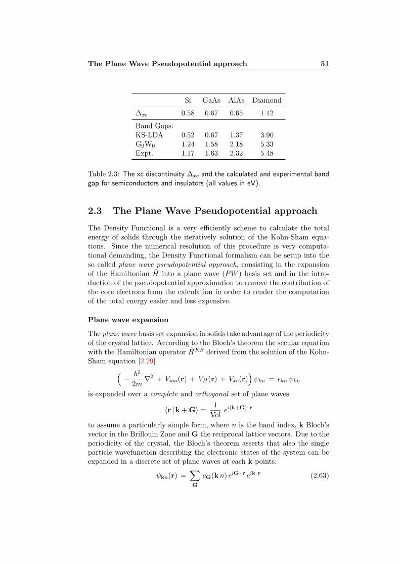
The Plane Wave Pseudopotential approach 51
Si GaAs AlAs Diamond
∆xc 0.58 0.67 0.65 1.12
Band Gaps:KS-LDA 0.52 0.67 1.37 3.90G0W0 1.24 1.58 2.18 5.33Expt. 1.17 1.63 2.32 5.48
Table 2.3: The xc discontinuity ∆xc and the calculated and experimental bandgap for semiconductors and insulators (all values in eV).
2.3 The Plane Wave Pseudopotential approach
The Density Functional is a very efficiently scheme to calculate the totalenergy of solids through the iteratively solution of the Kohn-Sham equa-tions. Since the numerical resolution of this procedure is very computa-tional demanding, the Density Functional formalism can be setup into theso called plane wave pseudopotential approach, consisting in the expansionof the Hamiltonian H into a plane wave (PW ) basis set and in the intro-duction of the pseudopotential approximation to remove the contribution ofthe core electrons from the calculation in order to render the computationof the total energy easier and less expensive.
Plane wave expansion
The plane wave basis set expansion in solids take advantage of the periodicityof the crystal lattice. According to the Bloch’s theorem the secular equationwith the Hamiltonian operator HKS derived from the solution of the Kohn-Sham equation [2.29]
(− ~
2
2m∇2 + Vion(r) + VH(r) + Vxc(r)
)ψkn = ǫkn ψkn
is expanded over a complete and orthogonal set of plane waves
〈r |k + G〉 =1
Volei(k+G)· r
to assume a particularly simple form, where n is the band index, k Bloch’svector in the Brillouin Zone and G the reciprocal lattice vectors. Due to theperiodicity of the crystal, the Bloch’s theorem asserts that also the singleparticle wavefunction describing the electronic states of the system can beexpanded in a discrete set of plane waves at each k-points:
ψkn(r) =∑
G
cG(kn) eiG · r eik· r (2.63)
52 2. Density Functional Theory
where the coefficient Cg have to be determined through the diagonalizationof the KS Hamiltonian in the new basis set:
∑
G′
HGG′(k) cG′(kn) = ǫkn cG(kn) (2.64)
where
HGG′(k) =1
2m| k+G |2 δG,G′+Vion(k+G,k+G′)+Vh(G−G′)+Vxc(G−G′)
(2.65)In this way the kinetic energy is diagonal and the potentials are describedin terms of their Fourier transforms, in particular, VH and Vxc are local inspace and don’t depend explicitly from k but only from the vectors of thereciprocal lattice through the relation G − G′. To note that if the crystalhas a center of inversion which is chosen as the origin, the secular equationis real, otherwise it’s necessary complex.
The Hamiltonian to diagonalize is a matrix whose size is determined by thenumber of elements, hence by the number of vectors G included in the expan-sion, that in principle are infinite when concerning with a periodic crystal.The coefficients cG(kn) with small kinetic energy (~2/2m) |k + G|2 give amore important contribution in the expansion than those with larger kineticenergy; also in the calculation of the density n(r) =
∑kn |ψkn(r)|2 f(εkn)
only the lowest eigensolutions are needed, converging as the dimension Nof the secular equation matrix. Nevertheless, since the diagonalization timeincrease as N3, one needs some limitation to the size of the matrix: thusthe plane wave basis set can be truncated neglecting the plane waves havingkinetic energy greater than the value imposed by some particular energy cut-off. This kinetic energy cutoff, applied to an infinite basis set, is expressedby
1
2|k + G |2 ≤ Ekin
and renders the plane wave expansion finite and discrete, but at the sametime, introduce some kind of errors in the final computed total energy. In-creasing the cutoff energy the magnitude of the errors will be reduce, improv-ing total energy convergence but slowlying down the computational time.It’s worth pointing out that since PWs are extended waves, they can’t wellreproduce localized functions such as the charge density around the nucleior even worse the orthogonalization wiggles of inner core states. In order todescribe features varying on a length of scale δ, one needs PW componentsup to q ∼ 2π /δ, that in a solid means ∼ 4π (2π/δ)3/ΩBZ (in Diamond,fcc lattice, PWs ∼ 250,000 are too much for practical use). The number ofplane waves Npw scales like
Npw ∝ Ω (Ecutoff )3/2

The Plane Wave Pseudopotential approach 53
Figure 2.3: Schematic illustration of a supercell geometry (a) for defect vacancyin a bulk crystal, (b) for a surface and (c) for an isolated molecule. The supercellboundaries are depicted by the dotted line.
Periodic Supercells
Since one deals with periodic infinite systems, in which holds the Bloch’stheorem, is convenient to simulate the systems with a periodically repeatedfictitious supercell. Periodic boundary condition are applied to the supercellin order to be reproduced throughout space accordingly to the periodicityof the systems along the three directions. The system cell is now large byconstruction: the primitive cell of the material is repeated ni times along thelattice vector a1,a2,a3, leading to cell of n1 × n2× n3 ×N0 atoms (where N0
is the number of atoms in the primitive cell). Accordingly, the Brillouin Zone(BZ) is reduced by a factor of ni in the respective directions. The cell canbe either the primitive unit cell of a crystal or a large supercell containinga sufficient number of independent atoms to mimic locally an amorphous, aliquid, but also a solid with point defect, surfaces or isolated molecules asillustrated in Fig. 2.3. When dealing with such a systems, slabs, isolatedmolecules or cluster and solids with point defects, is important to make thesupercell big enough in order to leave sufficient vacuum space around toavoid interaction between the periodic neighboring replica [103, 104].
Brillouin Zone K-point sampling
Through the plane wave expansion basis set the ”sum over the Brillouinzone k-points” is mandatory when calculating the charge density n(r) in aperiodic system and the related summation is made over an infinite numberof k-points:
n(r) =∑
k
∑
i
|ψk ,i(r) |2
When assuming the Born-Von Karman periodic boundary conditionsψ (r + LR) = ψ(r) (where L = L1 L2 L3 equals the numbers of cells of

54 2. Density Functional Theory
the crystal) the discrete sum become an integration over the BZ and theelectronic states are allowed only for a set of k-points whose density is pro-portional also to the volume of the solid. Through the Bloch theorem theelectronic state to calculated moves from infinite to a finite amount for ainfinite number of k-points. For insulator and semiconductors it has beenshown that the integral can be approximated by a discrete sum over an goodnumber of k-points. Symmetries can help to reduce the number of points:only one k-point is assigned to represent a so called star ( the set of k-pointsequivalent by symmetry) with a weight wi proportional to the number ofk-points in the set. Thus the infinite sum over the BZ is replaced by adiscrete sum over a set of points ki and weights wi:
1
L
∑
k
fk(r) →∑
i
wi fki(r)
The particular set of k-points are called ”special points” and can be ob-tained through different methods such as Chadi-Cohen [105] or Monkhorst-Pack [106] that afford to calculate total energy and electronic potential withaccuracy over a very small set of k-points. For counterpart, metals requiremore k-points for an accurate sampling over the BZ of the Fermi surface;thus one can use the tetrahedron method or a Gaussian broadening to treatproperly fractional occupation of metals.
Ab initio Pseudopotentials
The potential experienced by an electron in condensed aggregate of atomscan be divided into two main terms: the nuclei interaction potential and theelectron-electron interaction potential. Moreover also the electrons can beseparate into two regions with different characteristics: the region near thenuclei, the core region, contains the innermost tightly bound core electrons,which respond very little to the presence of neighboring atoms and do notplay a significant role in the chemical bindings of atoms, and the outermostremaining region in the atom containing the valence electrons which reallydetermines the chemical bindings of atoms, especially in metals and semicon-ductors. Thus the core electrons can be ignored reducing the atom to a ioniccore that interacts via an effective potential with the valence electrons: thisis the frozen core approximation. Thus the KS equation are resolved witha new effective potential interaction where the common all electrons-nucleiinteraction is replace by a ”fictitious” interaction between valence electronsand ionic core. This interaction that approximate the potential felt by thevalence electrons is called pseudopotential and was first introduced byEnrico Fermi in the 1934 [107], then developed around the 60-70’s throughthe empirical pseudopotential and the ab initio pseudopotential formulationby Phillips and Kleinman [108].

The Plane Wave Pseudopotential approach 55
The valence wavefunction have total energy higher than the core states andin the core region the valence electrons are far less likely to be found. How-ever since they experience the same Coulomb potential there and they musttherefore have an even higher kinetic energy, the states are here described asvery rapidly oscillating wavefunctions as a consequence of the strong ionicpotential in this region. These oscillations are at the origin of the orthog-onality between the core wavefunctions and the valence wavefunctionswhich is required by the exclusion principle:
∫drψc,k(r)∗ ψv,k(r) = 0 (in
the core region the oscillations have to interweave in order to give a vanishingintegral).
The pseudopotential formalism has grown out of the OrthogonalizedPlane Waves (OPW) methods developed in 1940 [109] by Herring andin which the valence wave functions are expanded in a set of a plane waves(PW) which are orthogonalized to all the core wavefunctions |ψc 〉 . In thisapproach the rapid oscillations of the wavefunction in the core region arecompensated via a plane wave expansion in the interstitial regions among thenuclei. Since the core states |ψc 〉 are rapidly oscillating around the nuclei,the valence wavefunctions |ψv 〉 will have strongly oscillations to guaranteethe orthogonality with respect the |ψc 〉 core. Then, to describe these rapidoscillations a great number of plane waves are needed with a huge computa-tional effort. However, if the core states don’t appear in the calculation onecan substitute the valence wavefunction with some pseudowavefunctionsidentical to the real wavefunction and with no nodes beyond some cutoffradius rc (r < rc).Defining the normalized plane wave |k 〉 as
|k 〉 =1√Ωeikr
the OPW χ is defined as a plane wave PW to which have been subtractedthe core orthogonality wiggles in the core region in order to be orthogonalto all the core wavefunctions ψcore
|χ 〉 = |k⟩−
core∑
c
ac |Ψc(r)⟩
= |k 〉−∑
c′
|ψc′⟩⟨ψc′ |k
⟩= (1− P)|k
⟩(2.66)
The valence wavefunction can be therefore expanded over the obtained OPWbasis set
|ψk,v 〉 =∑
G
avk+G |χk+G 〉 (2.67)

56 2. Density Functional Theory
with the orthogonality condition of the PW with all the core states:
〈Ψc |χ 〉 = 〈Ψc|k 〉 −core∑
c′
〈Ψc |Ψc′ 〉ac′ = 0
⇒ 〈Ψc|k〉 − δcc′ ac′ = 0
⇒ 〈Ψc|k 〉 =
core∑
c
ac (2.68)
Then substituting the explicit expression of OPW |χ 〉 in the expansion ofvalence wavefunction one gets
|ψk,v 〉 =∑
G
avk+G
[|k 〉−
∑
c
|ψc
⟩⟨ψc |k+G
⟩ ]= (1− P) |k+G〉 (2.69)
where G is the sum over the reciprocal lattice vectors that can be truncatedthrough the introduction of the cutoff energy. Defining a pseudowave-function ϕps
k like
|ϕpsk 〉 =
∑
G
avk+G |k + G 〉 (2.70)
we get
|ψk,v 〉 = |ψk,v 〉 +
core∑
c
avc |ψc 〉 = (1 − P) |ϕk 〉 (2.71)
One can see that the ”real” valence wavefunction can be expressed as thesum of two terms: (i) a smooth function, the pseudowavefunction and (ii)an oscillating term that results from the orthogonalization of the valence tothe inner core orbitals. Then, applying H to the valence states ψk,v gives
H|ψk,v 〉 = Ev |ψk,v 〉H (1 − P) |ϕps
k 〉 = Ev (1 − P) |ϕpsk 〉
H |ϕpsk 〉 − H P |ϕps
k 〉 = Ev |ϕpsk 〉 − Ev P |ϕps
k 〉[H + (Ev − H )P
]|ϕps
k 〉 = Ev |ϕpsk 〉 (2.72)
where defining H + (Ev − H )P = Hps as pseudohamiltonian gives
[H + (Ev − H )P
]|ϕps
k 〉 = H + (Ev − H )∑
c
|ψc 〉 〈ψc |ϕpsk 〉
= H +∑
c
[Ev − Ec
]|ψc 〉 〈ψc |ϕps
k 〉 (2.73)
Finally it results
[H +
∑
c
[Ev − Ec
]|ψc 〉 〈ψc|
]|ϕps
k 〉 = Ev|ϕpsk 〉 (2.74)

The Plane Wave Pseudopotential approach 57
from which it can be possible to extract the form of the pseudopotentialVps
V ps = V +∑
c
[Ev − Ec
]|ψc 〉 〈ψc (2.75)
The pseudopotential described here follows the formulation gives byPhillips and Kleinman [108] and can be view as a in term of with the fol-lowing main characteristics:
• it is spatially non local since it’s depends on r and r′ and it usesdifferent components in relation to different channels ℓ of angular mo-mentum and it is energy dependent since it depends on the eigenenergyof the state one wishes to find;
•∑
c
[Ev − Ec
]|ψc 〉 〈ψc
can be considered as a short-ranged repul-
sive correction to the ”real” long-ranged attractive potential V : nearthe core both parts completely cancel each other and the whole poten-tial is ”well-behaved” and weaker than the true potential near the coreaccording to the Phillips-Kleinman cancellation theorem; this impliesalso that the pseudowavefunctions are smooth and not oscillate inthe core region, as schematically shown in Fig. 2.4 .
• there exists also a normalization problem: although the valence pseu-dowavefunction |ϕps
k 〉 is globally normalized it doesn’t reproduce ex-actly the norm of the real wavefunction outside the core region. Fromthe condition 〈ψv|ψv〉 = 1 holds
1 = 〈ϕpsk |ϕps
k 〉 − 2∑ 〈ψc|ϕps
k 〉〈ϕpsk |ψc〉 +
∑c |〈ψc|ϕps
k 〉|2
(2.76)
⇒ 〈ϕpsk |ϕps
k 〉 = 1 +∑
c |〈ψc|ϕpsk 〉|2
this difference has to be connected with the so called orthogonalityhole. The lack of charge density between the valence and the coreregions produces this non norm-conservation behaviour giving rise toerrors and serious problem in the self-consistent calculations.
Since in this thesis work we had used the norm-conserving pseudopoten-tial to treat properly the optical features and the ultrasoft pseudopotentialthat allows to manage systems with several hundreds of atoms per unit cellin order to the structural and electronic properties, a brief resume of theirmain features will follow.
Norm-Conserving pseudopotential
The norm-conservation idea was introduce for the first time by Topp andHopfield [110] in 1974 in the context of empirical pseudopotential and then

58 2. Density Functional Theory
Figure 2.4: How the ”pseudo” appears : all-electron wavefunction and poten-tial (solid lines) and pseudopotential and pseudowavefunction (dashed lines).The cutoff radius at which the all-electron and pseudo- wavefunction match islabelled by rc
incorporated into the ab initio formulation by Hamman, Schluter and Chi-ang [111] in 1979 and then refined by Bachelet, Hamman and Schluter [112]in 1982. Generically the modern pseudopotentials are obtained invertingthe Schrodinger radial equation for a given reference configuration appliedto the all-electron (AE) wavefunction decomposed into a radial Rℓ and aspherical Yℓ,m (spherical harmonic) part and resolved in a self-consistentlyway:
ψAE(r) =∑
ℓ,m
RAEℓ Yℓ,m(Ω)
(− ~
2
2m
d2
dr2− l(l + 1)
2mr2+ V AE
KS (r)
)rRAE
ℓ (r) = ǫAEℓ r RAE
ℓ (r) (2.77)
where V AEKS is the KS self-consistent one electron potential containing all the
screening effects related both to core and valence electrons
V AEKS [nAE ](r) = −Z
r+ VHartree(r) + Vxc[n
AE ](r) (2.78)
Then the ”pseudization” process can be applied according to the followingquite general important conditions:

The Plane Wave Pseudopotential approach 59
1. the valence all-electron and pseudopotential eigenvalues have to beequal for a fixed initial atomic configuration:
ǫAEℓ = ǫps
ℓ (2.79)
2. the all-electron and the pseudo- wavefunction assume the same valuesbeyond a certain critical core cutoff radius rc(ℓ), which is stronglydependent by each angular momentum component ℓ:
RAEℓ (r) = Rps
ℓ (r) for r > rc(ℓ) (2.80)
in particular the pseudowavefunctions originating from the solution ofthe radial Schrodinger equation must be nodeless to guarantee smooth-ness and free of unwanted wiggles;
3. the spatial integrals for the all-electron and pseudo- charge densitymust give the same value for each radius r beyond rc(ℓ): this meansthat the pseudowavefunctions are forced to assure the same norm asthe true real wavefunction. This condition guarantees norm conserva-tion, the aim of this kind of pseudopotential.
∫ r
0r′
2 | RAEℓ (r′) |2 dr′ =
∫ r
0r′
2 | Rℓ(r′) |2dr′ r > rc(ℓ) (2.81)
According to these features, through the analytical inversion of the radialSchrodinger equation one obtains the screened pseudopotential :
wpsscr,ℓ(r) = ǫℓ −
ℓ(ℓ+ 1)
2r2+
1
2 r Rpsℓ (r)
d2
d r2[r Rps
ℓ (r)]
(2.82)
The screened pseudopotential wpsscr,ℓ(r) contains the effects due to the valence
electrons in VHartree and Vxc that have to be subtracted to yield:
wℓ(r) = wpsscr,ℓ(r) − VHartree[n
ps](r) − Vxc[nps](r) (2.83)
From the setting of the cutoff radius depends the quality of the pseudopo-tential. The smallest possible value is determined by the location of theoutermost nodal surface of the true all-electron wavefunctions. For cutoffradius close to the minimum, the pseudopotential is realistic and verystrong. For large cutoff radius, the pseudopotential is smooth and almostangular momentum independent, but therefore too unrealistic. A smoothpotential leads to a fast convergence of plane wave basis calculation.
The main features of the norm-conserving pseudopotentials are:
60 2. Density Functional Theory
• transferability: the needs to describe accurately the behaviour of thevalence electrons in several different chemical environments; this holdswhen the logarithmic derivative and the energy first order derivativeof the all-electron and pseudo- wavefunctions must be equal for eachr values beyond rc(ℓ) according to the identity:
−2π[(r Rℓ(r)
)2 d
dǫ
d
drln Rℓ(r)
]
r= 4π
∫ r
0[Rℓ(r) r]
2 dr (2.84)
and it assures that the scattering properties of the ionic core are wellreproduce like in the true all-electron atoms.
• non locality: due to construction there’s an explicit dependence onthe components of the angular momentum ℓ that can be expressedin terms of projection operator and angular coordinates in real spacewhere non locality behaviour is fully revealed:
V ps =∑
ℓ,m
| ℓm 〉V psℓ 〈 ℓm | =
∑
ℓ
Pℓ Vpsℓ
=∑
ℓ,m
|Yℓ m(Ω) 〉 V psℓ (r) 〈Yℓm(Ω′) | (2.85)
Outside the core radius the potentials Vℓ are identical for all the angu-lar momentum components of the wavefunction (this means non local).But Kleinman and Bylander found out the definition semi-local (sl),for the pseudopotential Vℓ which depends on the angular momentumbut not on | r | and | r′ | separately;
• separability: Kleinman and Bylander (KB) rewrote the semi-localpotential into a separable form in order to reduce the computationalcost. First the semi-local potential can be separated into a long-range(local Coulombian tail) and a short-range components:
wps(r r′) = wlocal(r) +∑
ℓ
∆wℓ(r)ℓ∑
m=−ℓ
Y ∗ℓm(r′)Yℓm(r)δ(r − r′)
︸ ︷︷ ︸nonlocal
(2.86)
where ∆wpsℓ,nl(r) = wps
ℓ − wpslocal (2.87)
and then the KB potential assumes the form:
wKB(r, r′) = wlocal(r) +∑
ℓ
∆wKBℓ (r, r′) =
= wlocal(r) +∑
ℓ
ℓ∑
m=−ℓ
ϕpsℓm(r)∆wℓ(r)∆wℓ(r
′)ϕpsℓm(r′)
∫d3r∆wℓ(r) |ϕps
ℓm(r) |2
(2.88)

The Plane Wave Pseudopotential approach 61
The wpsℓ,nl(r) is the ℓ angular momentum dependent component of any
non local pseudopotential, while wloc is a arbitrary component thatcan be use as a reference to produce accurate and transferable pseu-dopotentials. The KB potential is a norm-conserving pseudopotentialthat uses a single basis state for each angular momentum componentof the wave function projecting each spherical harmonic componentonto a single basis set. The pseudopotential in the form of Eq. [2.85]scales as Npw ×Npw while in the KB separable form of Eq. [2.88]like16Npw lnNpw.
Ultrasoft pseudopotentials
In 1990 David Vanderbilt [113] developed a new class of pseudopotentialin order to treat systems, such as transition metals, first-row elements orlarge-scale electronic structure problems, requiring hard pseudopotentialsto ensure transferability and demanding impractically large plane wave ba-sis sets. These new potentials are called ultrasoft pseudopotentials since theaim consists in a ”relaxation or softening” of the norm-conservation ruleand of the standard orthonormality constraint of atomic orbitals, then re-sulting in a wavefunction which can be expanded using a much smaller planewave basis set, as shown in Fig. 2.5. The orbitals are allowed to be as softas possible within the core region, and due to a energy cutoff lower thanthe common values for the norm-conserving pseudopotentials, this yields toa rapidly converging plane wave expansion due to . Nonetheless, the ul-trasoft pseudopotential must recover the same scattering properties of theall-electron potential expressed in terms of transferability and logarithmicderivative. The orthonormality is recovered by introducing a generalizedoverlap operator which depends on the ionic positions. The all-electrondensity is obtained by adding to the square modulus of the orbitals an”augmentation charge” localized in the core region.The first step consists in supplying the ”lack of charge density” in the coreregion through an augmented charge Qnm:
Qnm(r) = ψ†n
AEψm
AE − φ†nUSφm
US (2.89)
that corrects the charge density recovering the full valence value in this way:
n(r) =∑
i
|φUS
i |2 +∑
nm,I
QInm(r)〈φUS
i |βIn〉〈βI
m|φUSi 〉
(2.90)
The atomic pseudopotential is separated into a local Vloc and a nonlocalVnloc part. The non local potential is written in the separable form, as a

62 2. Density Functional Theory
Figure 2.5: ”True” pseudowavefunction strongly peaked inside the core region(solid line) and ”ultrasoft” pseudowavefunction modified in Vanderbilt’s scheme(dashed line).

The Plane Wave Pseudopotential approach 63
sum of projectors.
V US(r) = Vloc(r) + Vnloc(r)
V USnloc =
∑
nm
D(0)nm|βn〉〈βm |
with |βn〉 =∑
m
[εAEm − (T + Vloc)
]|φUS
m 〉〈φUS
m | [εAEm − (T + Vloc)] |φUS
n 〉 (2.91)
and D(0)nm = 〈φUS
n | [εm − (T + Vloc)] |φUSn 〉 + εmQnm −
∫Vloc(r
′)n(r′)dr
(2.92)
The local part (obtained removing the screening of Hartree and xc) withinthe core region is smooth, while the non local term is localized within thecutoff radius part since the β-projectors are limited to the core region itself.The orbitals are postulated to obey generalized orthogonality constraints〈ψn| S|ψn〉 = δ, with the non local overlap operator S given by:
S = 1 +∑
nm
|βn〉〈βm| (2.93)
then the KS equation is generalize in this way H|φUSi 〉 = εiS|φUS
i 〉 and thehamiltonian becomes
H = −~2∇2
2m+ Veff (r) +
∑
nm,I
DInm|βI
n〉〈βIm|
where the KS effective potential Veff = Vnloc +Vloc +VHartree +Vxc containsboth the local and the non local part.

64 2. Density Functional Theory
2.4 Excited states in DFT
The Hohenberg-Kohn theorem asserts that the ground-state densitydetermines the external potential. In this scheme it’s also possible toconnect the ground-state density with any excited state, thus conside-ring an excited-state energy as a functional of the ground-state density,allowing in principle DFT to calculate excitation energies. The ∆SCFis a method where the ground-state scheme is applied to calculate bothexcited and ground state as energy differences: practically, it’s based onthe energy difference between two self-consistent-field (SCF) calculations.The application of the DF formalism to the excited state can be justified ifapplied to the lowest-lying state for a given set of quantum numbers [114].As example, the ionization potential IP and electron affinity AE of a Nelectron system can be derived through a ∆SCF calculation as differencein total energy between two self-consistent calculations [115], as shown inSec. [2.2.2]. This method take into account the relaxation effects inducedby the removal or addition of an electron to the system. ∆SCF can yieldgood results when it is possible to simulate the excitations occupying justone-particle orbital; this immediately excludes the possibility to describethose excitations that are not easily described in terms of isolated singleparticle transitions. Furthermore, this method works in finite systems,but not in infinite ones. This because the main contribution in ∆SCF isthe Hartree relaxation, that for extended system is negligible and othercontributions, not described in this method, come out.
To describe neutral excitations [116, 117, 118, 118, 119, 120], ∆SCF yieldsto consider two different electronic configurations γi for the system, one forthe ground state ~γgs and another one for the excited state ~γexc:
• initial state: Ground State
~γgs =
γi = 1 i = 1, ..., Nγi = 0 i > N
• final state: Neutral Excited State
~γexc =
γi = 1 i = 1, ..., (h− 1), (h+ 1), ..., N and i = e (e > N)γi = 0 i = h and i > N, i 6= e
In the last configuration a particle-hole pair is considered in the systempromoting an electron from the valence band (i=h) to a conduction band(i=e). For this reason the method is also called constrained DFT. Theexcitation energy of the many-electron system, for which the excited stateshould be well described by single-orbital transitions, is the difference intotal energy, between two self-consistent calculation with the occupations

Excited states in DFT 65
described above, i.e.:Eexc = E~γexc
− E~γgs(2.94)
and this should then give the optical gap since the initial and final statesare still neutral.


3Many Body Perturbation Theory:
”a stairway to heaven”
E questo e il fiore del partigiano,morto per la liberta.
Bella Ciao, canzone della Resistenza
3.1 Theoretical Spectroscopies
Why the search for excited state calculation has become one of the mostimportant and thought challenge of the theoretical solid state research?The answer lies in the aim to developed theoretical instruments, day byday more powerful than the preceding ones, to understand the interactionbetween the scanning probe sources (electrons, light, X-rays, lasers, andother modern photon sources) and the matter in order to study materials,ranging from solids to atoms, from surface to nanoscale systems. The aimis the simulation through these theoretical tools of the electronic excitationsand, in general, of the all experimental spectroscopy techniques in orderto achieve a complete set of theoretical spectroscopy devices in order topredict with accuracy and to explain the experimental data (ellipsometry,EELS, Raman, IR, NMR, X-Ray, ARPES e ARPIES, STS, I/V transport,etc.).
In general it’s not sufficient to calculate ground-state properties in orderto interpret or predict results of experiments like photoemission, electron-energy loss, absorption, etc. Direct and inverse photoemission spectroscopiesconcern the study respectively of the occupied and empty states of the sys-tem, evaluating the energy of the photoelectron excited in or out the sample:
67

68 3. Many Body Perturbation Theory: ”a stairway to heaven”
this means that the consequent electron excitations leave the initial neutralN -electron system with N−1 electron (direct photoemission, in Fig. 3.1(a))or with N + 1 electron (inverse photoemission, in Fig. 3.1(b)). This excita-tions changing the number of electrons from N → N ± 1 and leaving thesystem in a charged state, are called charged excitations. On the other side,
(a) Direct photoemission: it offers a way toexperimentally investigate the occupied electronicstate. A monochromatic radiation (hν) is ab-sorbed by the sample, and a photoelectron fromthe valence band is emitted with energy Ek intothe vacuum.
(b) Inverse photoemission: investigation ofempty states. An electron with energy Ek is in-jected into the system in the conduction band anda photon hν is therefore emitted as a consequenceof the relaxation of the electron.
Figure 3.1: Charged excitations
spectroscopy techniques based on Optical Absorption (in Fig. 3.2(a)) andon energy loss (such as EELS) (in Fig. 3.2(b)),for example, take advantageof electronic neutral excitations which don’t change the number of electronsof the system. This means, in case of optical absorption, that the excitedelectron is just promoted from the valence to the empty states remainingwithin the sample, in contrast to what happen for the photoemission, asdepicted above. In case of EELS, the electrons are scattered inelastically bythe sample and lose their energy with the creation of collective electronicexcitations called plasmon, longitudinal collective excitation that cannot beexcited optically by transverse photons. Electron energy loss spectroscopycan be applied via different electronic microscopes, like TEM or SEM.
3.1.1 External Perturbation and dielectric function
The charged and neutral excitations of a system are related to the response ofthe system to an external perturbation represented by photons or electrons.From the theoretical point of view the interaction between the electromag-netic field generated by the probe and the matter can be treat as a weak

Theoretical Spectroscopies 69
(a) Optical Absorption: a photon hν ab-sorbed by the sample excite an electron from thevalence to the conduction band.
(b) Electron Energy Loss Spec-
troscopy:based on the inelastic scattering ofelectrons by the system under investigation.
Figure 3.2: Neutral excitations
classical perturbation to the quantum mechanical system. The electromag-netic field described through the vector potential A and the scalar potentialφ, enters in the interacting hamiltonian via the change of the velocity ope-rator p:
∑
i
1
2p2
i →∑
i
1
2
(pi ·
e
cA
)2
(3.1)
and working in the Coulombian gauge or velocity gauge(∇ ·A = 0), settingthe scalar potential φ = 0 for no external sources, neglecting the non-lineareffects, one gets the interacting hamiltonian
Hint → −ec
∑
i
A(ri, t) · pi (3.2)
that can be treated as a weak perturbation within time-dependent pertur-bation theory. The vector potential A can be written through the Fouriertransform in a plane wave form:
A(r, t) = A0ei(q·r−ωt) + c.c. (3.3)
where the Coulomb gauge is satisfied if k · A0(ω) = 0, so that A0(ω) isperpendicular to k, and the wave is transverse.
In the time-dependent perturbation theory, the probability per units oftime and volume for a transition at frequency ω is, at first order and forweak fields:
W (ω) = 2π∑
c,v,k,k′
|〈ck′|1cA · p|vk〉δ(εc(k′) − εv(k) − ω) (3.4)
70 3. Many Body Perturbation Theory: ”a stairway to heaven”
where |ck′〉 and |vk〉 denotes the single-particle Bloch states.In the previous expression we have to calculate the matrix elements of theperturbation between the Bloch states:
ǫ · 〈ck′|eiq·r · p|vk〉,
where A = A0ǫ.This expression can be simplified in many cases, expanding the exponentialeiq·r as:
eiq·r = 1 + (iq · r) +1
2(iq · r)2 + . . .
Since the wavelength q of light is small (∼ 5 ·10−2 nm−1) and the wavefunc-tions have a slowly dependence on k, it is possible to calculate the matrixelements in the dipole approximation, in this way only vertical transitionsare taken into account and since p = r = −i∇:
ǫ · 〈ck|p|vk〉 = −iǫ · 〈ck|∇|vk〉 = ǫ · 〈ck|r|vk〉 (3.5)
Now applying the Heisenberg equation of motion to the variable r, we have:
r = (i)−1[r, H0
](3.6)
where H0 is the unperturbed hamiltonian. If only local terms are present inH0:
〈ck|r|vk〉 = (i)−1〈ck|rH0 − H0r|vk〉 = (i)−1(εv(k) − εc(k))〈ck|r|vk〉 (3.7)
It is possible to derive now the relation between Eq. (3.4) and the opticalproperties of the system.Optical properties can be described by the complex macroscopic dielectricfunction εM = ε1 + iε2 and the complex refraction index N = n+ ik =
√ε
where n is the ordinary refraction index and k is known as the extinctioncoefficient.Thus the absorption coefficient α of a incident electromagnetic wave in thesample is related with Im εM in this way:
α(ω) =ωW (ω)
u cn
=ω
ncε2(ω) (3.8)
where u is the average energy density defined as u =n2A2
0ω2
2πc2and c
n is thespeed of light in the matter.Then it is possible to obtain for the imaginary part of the macroscopicdielectric function:
ε2(ω) =4π2
ω2
∑
c,v,k
|ǫ · 〈ck|p|vk〉|2δ(εc(k) − εv(k) − ω) (3.9)

Theoretical Spectroscopies 71
If the one-electron Hamiltonian H0 contains non-local terms, in particularwhen there’s a non-local component in the pseudopotential term, additionalterm must be included in Eq. (3.9) for the calculation of the spectrum:
r = v =−i~∇m
+i
~[VNL, r] (3.10)
In this way the length formula and the velocity formula differs only forthe non-local commutator between VNL and r operator [121]. In case of alongitudinal perturbation, the imaginary part of the macroscopic dielectricfunction is:
ε2(ω) = 4π2 limq→0
1
q2
∑
c,v,k
∣∣∣ 〈ck + q|eiq·r | vk〉∣∣∣2δ(εc(k+q)− εv(k)−ω) (3.11)
which is valid also in the case of non-local pseudopotential. Furthermorethe gauge invariance between the two different approaches has been demon-strated [122].
Linear Response of Optical Spectra
When the systems are investigated through spectroscopies the response tothe external perturbation used as a probe (being electrons for EELS or pho-ton for optical absorption or photoemission for example) can be described interms of the linear response approximation [123, 124]. The external pertur-bation potential Vext(r) induces a response of the system in terms variationof charge density and the total potential
δρind(r, t) =∫dr′ dt′ χ(r, r′ ; t− t′)Vext(r
′, t′)
Vtot =∫dr′ ǫ−1(r r′; t− t′)Vext(r
′) (3.12)
The total potential is screened because it contains the external potentialcontribution and the potential due to the polarization of the system inducedby the external perturbation:
Vtot = Vext + Vind (3.13)
where Vind(r, t) =∫dr′ ρind(r′,t)
| r−r′ | (3.14)
The χ function is called full reducible polarizability (i.e. the ρind is sensibleto the bare external potential Vext) and together with the irreducible polar-izability P are response functions describing how the ”polarization cloud”around the particle responds to the external perturbation, as in Fig. 3.3.The irreducible polarizability connects the induced charge density with thetotal potential:
ρind(r, t) =
∫dr dt′ P (r, r′ , t− t′)Vtot(r
′, t′) (3.15)

72 3. Many Body Perturbation Theory: ”a stairway to heaven”
Figure 3.3: The response of a polarizable medium to an external potential: theperturbation acts on the point charge in r0, inducing a potential δVext thatcreates an induced charge δρind acting again on the point charge. The wiggle,the polarizability, shows it response function.
Looking at the perturbed system in its ground state, the perturbation im-plies a redistribution of the charge (read wavefunction), that means depletionof charge (holes) or accumulation of charge (electrons) in some places. Thiscreation of electron-hole pairs, with consequent polarization of the medium,is reflected by the following equations
ε−1(r, r′;ω) = δ(r − r′) +
∫dr
′′
v(r − r′′
)χ(r′′
, r′;ω) (3.16)
ε−1(r, r′;ω) = δ(r − r′) −∫
dr′′
v(r − r′′
)P (r′′
, r′;ω) (3.17)
where v(r− r′′
) is a bare Coulomb interaction. When P is zero, the systemis not polarizable and hence the total potential is equal to the external one;otherwise P is in general and on the average negative, acting against theexternal potential. The two polarizability are related in this way, through aDyson-like equation
χ = P + P v χ (3.18)
that, introducing the Coulomb modified interaction term vG(q),
vr(q) =
0 G = 0vG(r) = 4π
|q+G |2G 6= 0.
become
χG,G′ = PG,G′ +∑
G′′
PG,G′′ vG′′ χG′′ ,G′ + PG,0 v0 χ0,G′ (3.19)

Theoretical Spectroscopies 73
Figure 3.4: Measurable quantities varying on a macroscopic scale. The averageis done over distances large compared to the cell diameter but small comparedto the wavelength of the external perturbation.
The ”real” quantity measured in spectroscopy is a macroscopic average(ǫM (ω)) of the microscopic dielectric function ǫm(r, r′ ω), that appears inthe Eq. [3.17]. The microscopic quantities, like total or induced fields, arerapidly varying quantities over the atomic scale and are averaged on a scalethat is large with respect to the crystal lattice cell dimension and smallerthan the wavelength of the perturbation, see Fig. 3.4. In the case of thedielectric function the correct quantity to average is ε−1(r, r′;ω) since oneis concerned with the total potential Vtot = ǫ−1 Vext for a given externalpotential and not vice versa. According to Adler and Wiser [125, 126], ina periodic system the macroscopic dielectric function εM (ω), in reciprocalspace is related to the zero-th element of the inverse microscopic dielectricmatrix εG,G′(q, ω)
εM (ω) = limq→0
1
ε−1G=0,G′=0(q, ω)
, (3.20)
where q denotes a vanishing wave vector with direction q belonging to thefirst Brillouin zone and G and G′ represent elements of the reciprocal Bra-vais lattice of the crystal; the limit q → 0 correspond to the dipole ap-proximation of Eq. [3.9]. The off-diagonal term in the dielectric matrixεG,G′(q, ω) reflects the non-homogeneity of the space and taking into ac-count the off-diagonal terms corresponds to include the so called local fieldeffects [127, 128, 129, 130]. All these off-diagonal elements contribute to the’head’ of the inverse dielectric matrix,
εG,G′ =
G = G′ = 0 G = 0(head) (wing)
G′ = 0 G, G′ 6= 0(wing) (body)
For homogenous media the microscopic dielectric matrix is a function of| r − r′ | and therefore εG,G′(q, ω) is diagonal in reciprocal space and the

74 3. Many Body Perturbation Theory: ”a stairway to heaven”
macroscopic dielectric function is calculated directly:
εM (ω) = limq→0
εG=0,G′=0(q, ω), (3.21)
otherwise it depends explicitly on the position r and r′ and, as said before,the matrix is not diagonal, and εM (ω) should be calculated through thecomplete inversion of the microscopic function. In this case all the elementsof the matrix contribute to one element of its inverse, reflecting then theeffects of local fields arising when there are inhomogeneities in the systemat the microscopic scale. Taking into account the local fields implies toconsider the realistic situation in which the scanning spectroscopy probeimpinging the sample in r affects the system inducing a perturbationin r′, thus generating differences between what one observes in r withrespect to the same measured in r′. Since the microscopic fields areaveraged over a region occupied by the electron, the contribution to thisaverage will be greater from those parts of the unit cell where the electronis more easily polarized. The macroscopic field is obtaining a spatialaverage of the microscopic quantity over the unit cell, resulting then an un-weighed averaged field differ from the local field, which is weighted averaged.
Moreover it is possible to show that another exact formulation of the macro-scopic dielectric function [131, 132, 133] is possible, where the inclusion ofthe local field is done straightforwardly by the insertion of the polarizabilityP :
εM = 1 − limq→0
[v0(q)PG=0,G′=0(q, ω)
](3.22)
The matrix PG,G′(q, ω) is the so called modified polarizability, and satisfiesthe Dyson-like screening equation with the irreducible polarizability P andthe modified Coulomb interaction v introduced in Eq. [3.1.1]:
P = P + P vP (3.23)
Through the modified polarizability the local fields are included in a straight-forward manner in the calculation of εM :
εM (ω) = 1− limq→0
[vG=0(q)
(1 − PG=0,G′=0(q, ω) vG=0(q)
)−1PG=0,G′=0(q, ω)
]
(3.24)Neglecting of local fields in Eq. [3.22] means not considering vG(q) inEq. [3.23], and is equivalent to set:
εM (ω) = limq→0
[1 − vG=0(q)PG=0,G′=0(q, ω)
]= lim
q→0εG=0,G′=0(q, ω) (3.25)
The modified polarizability P includes a correct inversion of the dielectricmatrix and at the same time it gives a formal representation very similar to

Theoretical Spectroscopies 75
that of Eq. [3.25]. Another point we want to stress is that the inclusion ofthe local field effects is independent of the different levels of approximationthat we use to calculate absorption spectra.The simplest approximation for the polarizability is the random phase ap-proximation (RPA), that consists to consider the zero-th order in the ex-pansion of P, that means to put P = P 0, where P= is the polarizability forthe non interacting electronic system. The RP approximation implies thatthe polarization is due only to the creation of an electron-hole pair, propa-gating independently, thus neglecting excitonic interaction between the twoparticles. In RPA the electronic transitions in the optical absorption spectraare treated as independent [122]. Moreover, when adding local fields, if thematrix inversion is properly taken into account, the independent transitionmix: even if no electron-hole interaction is included in P , there is an effectiveelectron-hole interaction term showing up in εM [131].
3.1.2 Electronic Spectra in practice
Within the KS-DFT scheme is possible to achieve a first example of elec-tronic spectra following the recipes give in the section before. The macro-scopic quantity measured to evaluate the optical absorption is the photoab-sorption cross section σph(ω):
σph(ω) =4πω
cIm α(ω) (3.26)
Since the dynamical polarizability α(ω) is defined as
α(ω) = −∫dr, dr′ Vext(r, ω)χ0(r, r′;ω)Vext(r
′, ω) (3.27)
then, σph is proportional to the imaginary part of χ, polarization function,which is related to the macroscopic averaged dielectric function in this way,ǫM = 1 − vχ0. The photoabsorption cross section is then directly propor-tional to the imaginary part of the χ response function and then to theimaginary part of the macroscopic dielectric function
σph(ω) ∝ limq→0
ω
cIm
v(q)χ0(q,q′;ω)
(3.28)
in the long wavelength limit q → 0. For what concern EELS, when anelectron impinges the sample, it loses energy by exciting electron-hole pairs,plasmons etc. The energy loss is given by the imaginary part of the integralof the potential generated by the electron and his induced charge. Theexternal potential Vext due to the scattered electron leads to a momentumtransfer q expressed by the loss function
L(ω) ∝ −Im ∫
dr dr′ e−iqr χ(r, r′;ω) eiqr′

76 3. Many Body Perturbation Theory: ”a stairway to heaven”
representing the energy loss by the electron per unit of time during thescattering process and which results in the end proportional to the imaginarypart of the inverse of the macroscopic dielectric function εM :
L(ω) ∝ − e
π2
∫dr
1
q2Im
ω
εM (q, ω)
(3.29)
Considering the Independent Particle RPA framework in which the elec-tronic transition are considered vertical and independent one gets:
Abs ∝ Im ε = Im1 − vχ0
= −v Im
χ0
(3.30)
EELS ∝ −Imε−1
= −v Im
χ0
1 − vχ0
=
ε2ε12 + ε22
(3.31)
and with χ0 in the IP-RPA approach defined as
χ0 = 2∑
c,v
| 〈φKSc | e−iq r |φKS
v 〉 |2
ω (ǫc − ǫv) + iη(3.32)
3.2 Quasiparticles and Green Functions approach
The excitations of system of strongly interacting particles can often be de-scribe in terms of quasiparticles. In solids a ”bare” electron repels other elec-trons via Coulomb potential that can be represented as a ”positively chargedpolarization cloud” surrounding the electron. This screening ”cloud” addedto the ”bare” electron contributes to the quasiparticle picture of electrons (asin Fig. 3.5), no more simple particles, but now quasi-particles weakly inter-acting with the neighbors via a screened Coulomb potential. Quasiparticlehas a finite lifetime since are only approximate eigenstates of the N -electronHamiltonian. The energy difference between quasiparticle and the bare par-ticle is usually described by the self energy Σ which account for all theexchange and correlation effects beyond the Hartree approximation. Theself-energy is a non-local, energy-dependent, and in general non-Hermitianoperator. The quasiparticles obeys to a Schroedinger-like equation, namedquasiparticle equation written as:[−1
2∇2 + Vext(r) + VH(r)
]ψ(r, ω)+
∫dr′ Σ(r, r′, ω)ψ(r′, ω) = E(ω)ψ(r, ω)
(3.33)
The one-particle Green function is defined as:
iG(1, 2) = 〈N | T[ψ(x1t1) ψ
†(x2t2)]|N〉 =
=
〈N | ψ(x1t1) ψ
†(x2t2) |N〉 for t1 > t2 electron
−〈N |ψ†(x2t2) ψ(x1t1) |N〉 for t2 > t1 hole(3.34)

Quasiparticles and Green Functions approach 77
Figure 3.5: A strong-interacting particles system can be mapped onto a KS non-interacting particle system (left side) or onto a weakly-interacting quasiparticle
system (right side) through a Green functions equation.
where (x1, t1) = (r1, ξ1, t1) = 1 and (x2, t2) = (r2, ξ2, t) = 2 . T is the Dysontime-ordering operator and ψ(x) is the field operator in the Heisenberg rep-resentation, |N〉 denotes the ground state of the interacting many-particlesystem. The one-particle Green’s function is called fermionic propagatorsince it describes the propagation of a fermion: for t2 > t1, gives the prob-ability amplitude that a hole created at (x1, t1) will propagate to (x2, t2)and for t1 > t2 the probability amplitude that an electron added at (x2, t2)will propagate to (x1, t1). The physical interpretation relates immediatelywith direct photoemission and inverse photoemission processes, because itdescribes the propagation of an electron or a hole in a many-electron sys-tem. The knowledge of the one-particle Green’s function gives observableproperties of large interest:
• The expectation value of any single-particle operator in the groundstate of the system;
• The ground-state energy of the system;
• The one-electron excitation spectrum of the system:
* Ei(N + 1) − E(N) = εN+1i → conduction bands
* E(N) − Ei(N − 1) = εN−1i → valence bands
For non interacting systems, the equation of motion, of the one-particle

78 3. Many Body Perturbation Theory: ”a stairway to heaven”
Green’s function G0(xt,x1t1) is:[i∂
∂t− h(x)
]G0(xt,x1t1) = δ(x − x1)δ(t− t1). (3.35)
In general, the equation of motion for an interacting ”two particle” Greenfunction is[i∂
∂t1−
(−1
2∇2
1 + Vext(1) + VH(1)
) ]G(1, 2)−
∫d3 Σ(1, 3)G(3, 2) = δ(1, 2)
(3.36)Then introducing a new mass operator M including the whole many-bodyinteraction (self-energy and Hartree potential) that Σ = M − VH one gets
[i∂
∂ t1+
1
2∇2
1 − Vext
]G(1, 2) −
∫d3M(1, 3)G(3, 2) = δ(1, 2) (3.37)
where, applying the condition Σ = 0, comes out the equation for the non-interacting Green function G0:
[i∂
∂t1−
(−1
2∇2
1 + Vext(1) + VH(1)
) ]G0(1, 2) = δ(1, 2) (3.38)
The Green function satisfies also a Dyson-like [134, 135] equation that yieldscombining Eq.s [3.36] and [3.38]:
G(1, 2) = G0(1, 2) +
∫d(34)G0(1, 3) Σ(3, 4)G(4, 2) (3.39)
3.2.1 Quasiparticle representation and Spectral Function
Through the ”resolvent theory” [136, 137] 1 the Green function can be ex-pressed in terms of the quasiparticle wavefunctions and energies via its spec-tral function A thus clarifying its physical relevance. The spectral represen-tation of G in the frequency domain is:
G(r, r′, ω) =∑
i
Ψi(r, ω)Ψ∗i (r
′, ω)
ω − ǫi(ω)(3.40)
where the quasi-particle eigenvalues ǫi(ω) are in general complex: the realpart has the physical meaning of the energy required to excite the system,while the imaginary part is associated to the dumping of the excited stateand therefore to its lifetime. This is strictly related to the imaginary partof the Green function, called spectral function:
A(r, r′, ω) = − 1
πIm
G(r.r′, ω)
(3.41)
1Given (z −L) |u〉 = |f〉, with L differential operator, the Green function is the inverse ofthe associated homogenous equation, G(z) = (z − L)−1
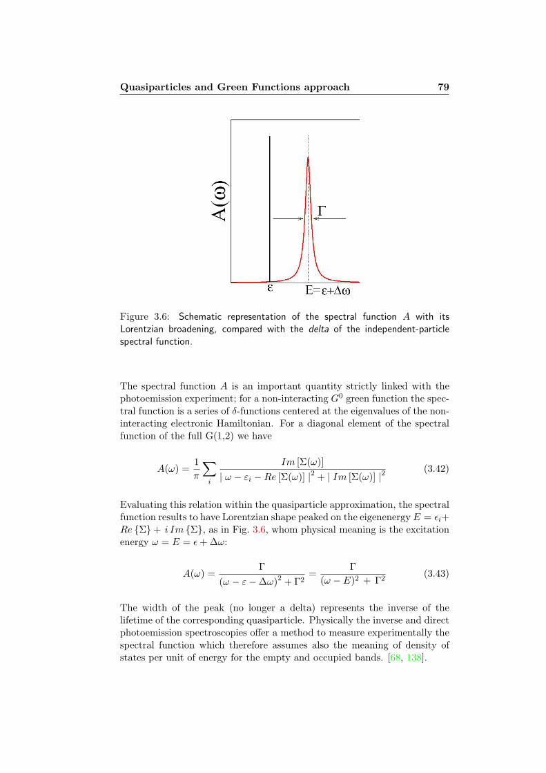
Quasiparticles and Green Functions approach 79
Figure 3.6: Schematic representation of the spectral function A with itsLorentzian broadening, compared with the delta of the independent-particlespectral function.
The spectral function A is an important quantity strictly linked with thephotoemission experiment; for a non-interacting G0 green function the spec-tral function is a series of δ-functions centered at the eigenvalues of the non-interacting electronic Hamiltonian. For a diagonal element of the spectralfunction of the full G(1,2) we have
A(ω) =1
π
∑
i
Im [Σ(ω)]
| ω − εi −Re [Σ(ω)] |2 + | Im [Σ(ω)] |2(3.42)
Evaluating this relation within the quasiparticle approximation, the spectralfunction results to have Lorentzian shape peaked on the eigenenergy E = ǫi+Re Σ+ i Im Σ, as in Fig. 3.6, whom physical meaning is the excitationenergy ω = E = ǫ+ ∆ω:
A(ω) =Γ
(ω − ε− ∆ω)2 + Γ2=
Γ
(ω − E)2 + Γ2(3.43)
The width of the peak (no longer a delta) represents the inverse of thelifetime of the corresponding quasiparticle. Physically the inverse and directphotoemission spectroscopies offer a method to measure experimentally thespectral function which therefore assumes also the meaning of density ofstates per unit of energy for the empty and occupied bands. [68, 138].

80 3. Many Body Perturbation Theory: ”a stairway to heaven”
3.2.2 An ”alchemic circle”: the Hedin’s pentagon
In order to solve numerically the problem of an interacting many-electronsystem, one-particle equations are very often used: for example the Kohn-Sham equations, the Hartree-Fock equations, the quasi-particle equations.The main difference among these lies in the description of the many-bodyinteraction which in the Hartree-FocK theory is described through an ex-change potential vx, in DFT through an exchange-correlation potential vxc
and in the Green’s function approach the self-energy operator Σ contains theinformation on the electron-electron interaction. The self-energy is a morecomplicated object with respect to vxc or vx. In fact it is energy dependent,
Figure 3.7: Sketch of the coupled integral Hedin equation.
non-local in space and non Hermitian. In 1965, Lars Hedin proposed anexpansion of Σ in term of the Coulomb screened potential W , via a schemeof five coupled integral equations (see Fig. 3.7):
• Vertex function
Γ(1, 2, 3) = δ(1, 2)(2, 3)+
∫d(4, 5, 6, 7)
δΣ(1, 2)
δG(4, 5)G(4, 6)G(7, 5) Γ(6, 7, 3)
(3.44)
• Irreducible polarizability
P (1, 2) = −i∫d(3, 4)G(1, 3) Γ(3, 4, 2)G(4, 1+) with 1+ = (r1, σ1, t1+δ)
(3.45)
• Screened interaction
W (1, 2) = v(1, 2) +
∫d(3, 4) v(1, 3) P (3, 4)W (4, 2) (3.46)
Quasiparticles and Green Functions approach 81
• Self energy
Σ(1, 2) = i
∫d(3, 4)G(1, 3+)W (1, 4) Γ(3, 2, 4) (3.47)
• Dyson equation
G(1, 2) = G0(1, 2) +
∫d(3, 4)G0(1, 3) Σ(3, 4)G(4, 2) (3.48)
At this point we want to obtain from these equations the response functionsof the system to the external perturbation. The inverse dielectric functionis given as:
ǫ−1(1, 2) =δV (1)
δw(2), (3.49)
ǫ−1(1, 2) = δ(1, 2) +
∫d 3v(1, 3)
δρ(3)
δw(2)(3.50)
and we can define the response function or reducible polarizability as:
χ(1, 2) =δρ(1)
δw(2)(3.51)
which gives the change in the charge density upon a change in the externalpotential.The polarization function or irreducible polarizability is defined instead asthe change in the charge density upon a change in the total potential:
P (1, 2) =δρ(1)
δV (2). (3.52)
Then it is possible to write the dielectric matrix and the inverse dielectricmatrix as:
ǫ−1(1, 2) = δ(1, 2) +
∫d 3v(1, 3)χ(3, 2), (3.53)
ǫ(1, 2) = δ(1, 2) −∫d 3v(1, 3)P (3, 2), (3.54)
where the relation between the two response functions is:
χ(1, 2) = P (1, 2) +
∫d3 d4P (1, 3) v(3, 4)χ(4, 2). (3.55)
Finally, we show the relation of the screened potential with the irreducibleand reducible polarizabilities:
W (1, 2) =
∫d 3 ε−1(1, 3)v(3, 2)
= v(1, 2) +
∫d 3d 4v(1, 3)P (3, 4)W (4, 2)
= v(1, 2) +
∫d 3d 4v(1, 3)χ(3, 4)v(4, 2) (3.56)

82 3. Many Body Perturbation Theory: ”a stairway to heaven”
3.2.3 The GW Approximation
This approximation (GWA) consists in a shortcut of the Hedin’s equationspentagon, avoiding the calculation of the vertex function set to unity. Thusthe self energy is calculated as the product of the self-consistent single-particle propagator G0 and the self-consistent dynamically screened interac-tion W . The GWA corresponds to the first iteration of the Hedin equations,that means to neglect the higher-order vertex corrections, and can be in-terpreted as the first-order term of the expansion of the self-energy Σ inrelation to the screened interaction:
Γ(1, 2, 3) = δ(1, 2)δ(1, 3), (3.57)
and the polarizability becomes
P (1, 2) = −iG(1, 2+)G(2, 1). (3.58)
This is the so called Random Phase Approximation (RPA) for P : the po-larizability is the product of two one-particle Green’s functions. A form forthe screened Coulomb potential W can be obtained, finally giving the lowestorder contribution in W to the self energy:
P 0(1, 2) = −iG0(1, 2)G0(2, 1+) (3.59)
W 0(1, 2) = v(1, 2) +
∫d(3, 4)v(1+, 3)P 0(3, 4)W 0(4, 2) (3.60)
Σ(1, 2) = iG0(1, 2)W 0(1+, 2) (3.61)
This self-energy ΣGWA = G0W 0 is used to calculate the quasi-particleenergies through the quasi-particle equation; in practical calculations theone-particle Green function is calculated as the independent particle Greenfunction G0 and in the zeroth order for Γ it is possible to obtain: P ,W andΣ. Starting from the initial KS eigenvalues one gets
Eqpi = εKS
i + 〈φLDAi | Σ(Eqp) − V LDA
xc | φLDAi 〉 (3.62)
where the Eqp appear also as argument of the self-energy itself which ex-panded in Taylor series, at the first-order term around the εKS
i
〈Σ(Eqp)〉 = 〈Σ(εKS)〉 + (Eqpi − εKS
i )〈∂Σ(ω)
∂ω〉ω=εKS
i
+O[(Eqp
i − εKSi )
2]
(3.63)gives the GW corrections (at the first-order) with respect to the KS energies:
Eqpi − εKS
i =〈Σ(εi)〉 − 〈Vxc〉
1 − 〈∂Σ(ω)∂ω 〉
ω=εKSi
= Zi [〈Σ(εi)〉 − 〈Vxc〉] (3.64)

The Bethe-Salpeter approach 83
The standard GW approximation represents a valid tool to estimate theΣ obtaining accurate results for excitation energies and quasi-particle bandgaps of solids [139, 140, 141, 142]. In order to go beyond, fully or partialself-consistent GW calculation can be performed [143, 144, 145, 146, 147,148, 149, 150, 151, 142].
3.3 The Bethe-Salpeter approach: an effective
Two-Particle Equation
Starting from the Hedin’s equation it is possible to obtain a four-point equa-tion for the polarizability and the problem can be reformulate in terms of aneigenvalue problem with an effective Hamiltonian describing the excitonicinteraction. For a more detailed derivation of the two-particle Hamiltoniansee:[131, 132] .The starting point is the irreducible polarizability of Eq. (3.45) in GW ap-proximation which contains, through the vertex function, an intrinsic four-point quantity:
δΣ(1, 1, 1′)
δG(2, 2′)=δ(iG(1, 1′)W (1, 1′))
δG(2, 2′)=
= iδG(1, 1′)
δG(2, 2′)W (1, 1′) + iG(1, 1′)
δW (1, 1′)
δG(2, 2′), (3.65)
where the term iG(1, 1′) δW (1,1′)δG(2,2′) is usually neglected.
To describe the propagation of an electron-hole pair we need four-point quan-tities, and so it is convenient to define the four-point screened interactionas:
W (1, 1′; 2, 2′) = W (1, 1′)δ(1, 2)δ(1′, 2′), (3.66)
and the four-point independent particle polarizability:
P 0(1, 1′; 2, 2′) = −iG(1′, 2′)G(2, 1). (3.67)
It is possible to insert Eq (3.65) in the Eq (3.45) and a generalized four-pointirreducible polarizability is obtained as:
P (1, 1′, 2, 2′) = P0(1, 1′, 2, 2′)+
−∫P0(1, 1
′, 3, 3′)W (3, 3′, 4, 4′)P (4, 4′, 2, 2′) d 3 d 3′ d 4d 4′, (3.68)
where only the attractive screened interaction W appears.With the same considerations, we can obtain a generalized four-point formfor the modified polarizability and for the response function:
4χ =4 P +4 P 4v4χ,

84 3. Many Body Perturbation Theory: ”a stairway to heaven”
4P =4 P +4 P 4v4P .
Also the Coulomb potential now is a four-point quantity and the same holdsalso for the modified Coulomb potential:
v(1, 1′, 2, 2′) = v(1, 2)δ(1, 1′)δ(2, 2′). (3.69)
The explicit form for the response function is:
χ(1, 1′, 2, 2′) = P0(1, 1′, 2, 2′) +
∫P0(1, 1
′, 3, 3′)×[v(3, 3′, 4, 4′ −W (3, 3′, 4, 4′)
]P (4, 4′, 2, 2′) d 3 d 3′ d 4d 4′, (3.70)
while the modified polarizability is:
P (1, 1′, 2, 2′) = P0(1, 1′, 2, 2′) +
∫P0(1, 1
′, 3, 3′)×[v(3, 3′, 4, 4′ −W (3, 3′, 4, 4′)
]P (4, 4′, 2, 2′) d 3 d 3′ d 4d 4′. (3.71)
The only difference between the Eqs. (3.70) and (3.71) is the long range tailof the Coulomb potential which is responsible for the local-field effects [131].The macroscopic dielectric function with the inclusion of the electron-holeinteraction is:
εM (ω) = 1 − limq→0
[vG=0(q)
∫drdr′e−iq(r−r′)4P (rr, r′r′;ω)
], (3.72)
where now P has been contracted to a two-point quantity.Actually the creation and the annihilation of the electron-hole pairs canbe considered simultaneous and the interaction instantaneous. Taking intoaccount the translational invariance in time it is possible Fourier transformto the frequency space:
χ(1, 1′, 2, 2′) = χ(x1t1,x1′t+1 ,x2t2,x2′t
+2 ) = χ(x1,x1′ ,x2,x2′ , t2 − t1)
→ χ(x1,x1′ ,x2,x2′ , ω)δ(x1 − x1′)δ(x2 − x2′).
Another approximation commonly used: is the energy dependence of thescreened potential is neglected and one assumes W (ω) = W (ω = 0) [152].Equation (3.71) for the modified polarizability has a Dyson-like form, justconsidering the lowest order of the interaction kernel.It is possible to invert the polarizability for each frequency ω, but this isvery often too demanding. The problem of inverting the matrix can betransformed in an eigenvalue problem, where the electron-hole interactionis described through an effective two-particle Hamiltonian.

The Bethe-Salpeter approach 85
The one-particle models can not describe the presence in the experimentalspectra of resonance-like structures at low frequency (bound-excitons) andusually may lead too low optical absorption intensities [131]. It is thennecessary to include the electron-hole interaction in the calculations. Wefirst assume that the excited state can be obtained by a coherent linearsuperposition of vertical single-pair excitations plus corrections of higherorder:
|E〉 =∑
c,v,k
Acvka†ck ˆavk|0〉 + |C〉. (3.73)
|E〉 is an eigenstate of an ”unknown” excitonic Hamiltonian and the exci-tonic energy Ω can therefore be calulated as:
H|E〉 = Ω|E〉. (3.74)
Considering only the linear part of |E〉 in the single-particle transition, it isalso possible to write |E〉 on the basis of single-particle orbitals:
Ψ(r, r′) =∑
cvk
ψqpck(r)ψqp∗
vk (r′). (3.75)
The excitation energies are the solutions of an eigenvalue problem andit is necessary to find a form of the effective two-particle hamiltonian ofEq. (3.74).In order to derive the form of the Hamiltonian of the eigenvalue problem ofEq. (3.74) the first step is to change the basis of the quantity we are deal-ing with and consider as a new basis that of a single-particle eigenfunctionsφn(x).In this basis any four point quantity is:
S(x1,x1′ ,x2,x2′) =∑
(n1,n′1)(n2,n′
2)
φ∗n1(x1)φn′
1(x1′)φn2
(x2)φ∗n′
2(x2′)S(n1,n′
1)(n2,n′
2), (3.76)
the modified polarizability now becomes:
P(n1,n′1)(n2,n′
2) = P 0
(n1,n′1)(n2,n′
2)+
P 0(n1,n′
1)(n3,n′
3)Ξ(n3,n′
3)(n4,n′
4)P(n4,n′
4)(n2,n′
2), (3.77)
where the interaction kernel is defined as:
Ξ(n1,n′1)(n2,n′
2) =
−∫dx1dx1′φn1
(x1)φ∗n′
1(x1′)W (x1,x1′)φ
∗n2
(x1)φn′2(x1′)+
+
∫dx1dx1′φn1
(x1)φ∗n′
1(x1)v(x1,x1′)φ
∗n2
(x1′)φn′2(x1′). (3.78)
86 3. Many Body Perturbation Theory: ”a stairway to heaven”
The independent-particle response function polarizability is:
χ0 (n1,n′1)(n2,n′
2) = δ(n1,n2)(n′
1,n′
2)
fn′1− fn1
En′1− En1
− ω(3.79)
and fn are the occupation numbers.The modified polarizability takes the form [131]:
P(n1,n′1)(n2,n′
2) = (H2p − Iω)−1
(n1,n′1)(n2,n′
2)(fn′
2− fn2
) (3.80)
where H2p is:
H2p(n1,n′
1)(n2,n′
2)
= (En′1− En1
)δ(n1,n2)(n′1,n′
2) + (fn1
− fn′1)Ξ(n1,n′
1)(n2,n′
2).
(3.81)
At this point we can apply an identity which holds for a system of eigenvec-tors and eigenvalues of a general, non hermitian matrix, that is:
(H2p − Iω)−1(n1,n′
1)(n2,n′
2)=
∑
µ,µ′
A(n1,n′
1)
µ M−1µ,µ′A
∗ (n1,n′1)
µ′
(Eµ − ω), (3.82)
A(n1,n′
1)
µ and Eµ are obtained solving the following eigenvalue problem:
∑
(n1,n′1)(n2,n′
2)
Hexc(n1,n′
1)(n2,n′
2)A
µ(n2,n′
2)= EµAµ
(n1,n′1). (3.83)
The overlap matrix Mµ,µ′ between the eigenstates (which are in general nonorthogonal) can be written as:
Mµ,µ′ =∑
(n1,n′1)
A(n1,n′
1)
µ A∗ (n1,n′
1)
µ′ . (3.84)
The polarizability is obtained solving Eq. (3.83), it is possible to obtain thepolarizability and therefore the macroscopic dielectric function.Considering a two-point contraction of the polarizability in real space andFourier transforming, the macroscopic dielectric function becomes:
εM = 1 − limq→0
v0(q)∑
µ,µ′
∑
(n1,n′1)
〈n1|e−iqr|n′1〉A(n1,n′
1)
µ ×
M−1µ,µ′
∑
(n2,n′2)
〈n′2|eiqr′ |n2〉A∗(n2,n′2)
µ′
(fn′2− fn2
)
(Eµ − ω). (3.85)
This expression can be simplified analyzing the form of the effective Hamil-tonian H2p
(n1,n′1)(n2,n′
2).

The Bethe-Salpeter approach 87
The index n1 = (n,k) contains the information of the band (valence or con-duction) and of the k point which labels the corresponding single-particlestate, but considering that we are dealing only with vertical transitions, thatis k is fixed, from now on we will omit this index.In what follows we will use this notation:
• (n1, n′1):
– unoccupied state: v1,v1′
– occupied state :c1,c1′
• (n2, n′2):
– unoccupied state: v2,v2′
– occupied state : c2,c2′
the matrix representation of the two-body Hamiltonian H2p(n1,n′
1)(n2,n′
2)
is:
v2, c2 c2, v2 v2, v2′ c2, c2′
v1, c1 H2p(v1 c1)(v2 c2) Ξ(v1 c1)(c2 v2) Ξ(v1 c1)(v2 v2′ )
Ξ(v1 c1)(c2 c2′ )
c1, v1 −Ξ(c1 v1)(v2 c2) −H2p(c1 v1)(c2 v2) −Ξ(c1 v1)(v2 v2′ )
−Ξ(c1 v1)(c2 c2′ )
v1, v1′ 0 0 (Ev1′− Ev1
)δ(v1,v2)(v1′ ,v2′ )0
c1, c1′ 0 0 0 (Ec1′ − Ec1)δ(c1,c2)(c1′ ,c2′ )
In the definition of H2p(n1,n′
1)(n2,n′
2)
there are δ(n1,n2)(n′1,n′
2); which is the
identity in the transition basis, and (fn1− fn′
1), which is different from
zero only for those transitions for which (n1, n′1)=(occupied,unoccupied) or
(n1, n′1)=(unoccupied,occupied).
Despite the simplifications, the form of the H2p is quite complicated, but itis interesting to note that in the polarizability appears: (fn′
2− fn2
).(fn′
2−fn2
) contributes only for the terms corresponding to (v2 c2) and (c2 v2),
then we can obtain Hexc,2p(n1,n′
1)(n2,n′
2):
H2p resonant(v1 c1)(v2 c2) Ξcoupling
(v1 c1)(c2 v2)
−[Ξcoupling
(v1 c1)(c2 v2)
]∗−
[H2p resonant
(v1 c1)(v2 c2)
]∗
TheH2p resonant is Hermitian and corresponds to positive absorption energy,while −
[H2p resonant
]∗is the anti-resonant part, and gives the de-excitations
energies [152]. In the calculations of optical spectra the coupling part of the
88 3. Many Body Perturbation Theory: ”a stairway to heaven”
matrix is often neglected (Tamm-Dancoff approximation).In this approximation the eigenvalue problem can be rewritten as:
∑
(v2 c2)
Hexc,2p resonant(v1 c1)(v2 c2) Aµ
(v2 c2) = Eexcµ Aµ
(v1 c1), (3.86)
and finally Eq. [3.85] can be simplified:
εM = 1 − limq→0
v0(q)∑
µ
∑
(v1 c1)
|〈v1|e−iqr|c1〉A(v1 c1)µ |2
Eexcµ − ω − iη
(3.87)

4The Systems
L’ Italia e una Repubblica democraticafondata sul lavoro.La sovranita appartiene al popolo, che laesercita nelle forme e nei limiti dellaConstituzione
Constituzione Italiana, Art. 1
In this section we will present and comment the results obtained throughthe computer numerical simulations realized during my three year of PhDfellowship. The numerical simulation have been realized through severalab initio DFT code within the plane-wave pseudopotential approach, suchas Pwscf [153], VASP [154, 155] and Abinit [156] for what concern thetotal energy calculation part. On the other side, the optical features of thesystem have been investigated through different codes, like SELF [157] andEXC [158]. Due to the very huge computational cost of the simulations, thetotal energy and the many body optical calculations have been performedon supercomputing machines located at the CINECA computing center inBologna and at CICAIA center in the University of Modena and ReggioEmilia.
4.1 Model System
This chapter is devoted to the description of 0-dimensional Silicon crystal,commonly called Silicon nanocrystals (Sinc). The Sinc described in thiswork are spherical nanocrystals isolated in vacuum and doped simultane-ously with substitutional impurities of Boron and Phosphorus. Startingpoint of this study are the undoped Sinc, free-standing nanocrystals builtup by considering all the bulk Silicon atoms contained in a sphere centered
89

90 4. The Systems
Figure 4.1: Schematic representation of the supercell approach. The supercellis represented by the continuous grey line and the atoms by the spheres (topview). The Sinc into account is the Si147H100. As one can see the physicalnanocrystal is in the center of the image, while nc appearing in the corners arefictitious replicas introduced by the supercell approach.
on a Si ion; they show an almost spherical shape, the typical tetrahedralcoordination of bulk Silicon for the Si-Si bond distances and have Td pointgroup symmetry of the typical diamond-structured bulk materials.
The present work takes into account different nanocrystals with diame-ters ranging from 1.1 nm up to 1.79 nm, in order to simulate almost re-liable systems through the progressively increasing of dimensions. The un-doped Sinc considered, the Si35H36 (d=1.10 nm), Si87H76 (d=1.5 nm),Si147H100 (d=1.79 nm) are passivated at surface with hydrogen to saturateall the possible dangling bonds and to exclude possible effects of surfacestates and surface reconstruction. The single and codoped Sinc, instead,are obtained from the above nanocrystals with the insertion of one or twoimpurities, a donor atom (such as Phosphorus) and an acceptor one (likeBoron) placed in substitutional site after the removal of the corresponding Siatom. All the Sinc are treated as isolated free standing nanocrystals placedinto simple cubic supercells, with side varying from 40 a.u. up to 45 a.u.,according to the nc diameter (respectively the former for the Si35H36 andthe later for the Si87H76 and Si147H100 ) in order to leave enough vacuum (at

Formation Energy 91
least 6 A) around each neighboring nanocrystals to avoid any Coulombianinteraction between the periodic replica, as shown in Fig. 4.1. The bandfolding in the Brillouin Zone and the flattening of the bands into discretelevels without any k-dispersion due to the quantum confinement along the3 coordinate directions, allow to sample the Brillouin Zone only with thesingle Γ (0,0,0) k-point.
The total energy calculation, have been performed using an energy cut-off of 30 Rydberg (Ry), treating the structural relaxation with ultrasoftVanderbilt pseudopotential in order to manage large supercells with a hugenumber particles up to 512 atoms, while the optical properties have been cal-culated via norm-conserving pseudopotential in the formulation of Perdewand Zunger [79]. The application of ultrasoft pseudopotential for opticalcalculations is problematic both for the relaxation of the norm conserva-
tion and also for the presence of the non-local commutator p = i~
[H, r
]
that does not permit an accurate and an easy computing description. TheXC functional used is GGA in the formulation of Perdew-Burke-Ernzerhof(PBE) [74] very similar to the PW91 pseudopotential (see Section 2.2.1).
4.2 Formation Energy
When defects are present or created in the materials, the systems subduea perturbation. In our case defects are represented by acceptor and donorimpurities, such as Boron (B) and Phosphorous (P) respectively, substitu-tionally inserted in the hydrogenated Sinc. Our aim is to understand whichconfiguration is more stable when one or two impurities are inserted, and inpractice to evaluate what amount of energy is required to sustain the dop-ing process. A theoretical useful tool is the Formation Energy (FE) defined,according to the paper of Zhang and Northrup [159], and applied in severalothers papers [160, 161, 162] with the following formulation:
∆EFE = E (Sin−l−kBkPlHm)−E (SinHm)+ (k+ l)µSi − k µB − l µP, (4.1)
The k and l index can be 0 or 1, thus one has an un-doped, a single B- orP-doped Sinc or a B and P co-doped Sinc. The Formation Energy of neutralB and/or P impurities can be defined as the energy required to insert oneB and/or one P atom within the cluster after removing one (or two) Siatoms (depending on single doping or co- doping) which are transferred tothe chemical reservoir, assumed to be bulk Si. Here we’re calling FormationEnergy the amount ∆FE even if this is just an energy difference ∆FE =Ef2
− Ef1, between the formation energy of the pure undoped Sinc
Ef1= E (SinHm) − nµSi −mµH (4.2)

92 4. The Systems
and the Formation Energy of the doped nanocrystals (with one or two im-purities)
Ef2= E (Sin−l−kBkPlHm) − (k + l)µSi − k µB − l µP −mµH (4.3)
To evaluate this amount ∆FE one has just to perform total energy calculationof the system energy E (with and without impurities) and of the chemicalpotentials for each of the atomic species involved in the formula [4.1]: µSi isthe total energy per atom of bulk Si, µB the total energy per atom in tetra-gonal B50 for the Boron impurity, as in [163] and µP the chemical potentialin Orthorhombic Black Phosphorus for P impurity, as in [164]. Since thequantity ∆FE is independent by the number of atoms of the nanocrystals,it can be calculated and compared for several Sinc of different size, givinga measure of the stability of the single and co- doped Sinc with respectto several parameters, such as the dimensions, the number of the chemicalspecies and the relative position of impurities within the nanocrystals.
4.3 What about doping Silicon Nanocrystals?
The semiconductors doping has represented since the 70’s a valid and cheaptechnique to increase the number of carriers of the system. This holds forSilicon in particular because of its intense application in the traditional mi-croelectronics field. Hundreds of papers investigating doping Bulk Silicon arepresent in the literature, but none of them since last 10 years has concernedthe possibility to dope Silicon based nanostructures. In particular, prelimi-nary research works have been presented in international scientific journalsby the experimental group of Minoru Fujii since 1998, indicating the way toachieve stimulated emission of visible light from small Silicon nanocrystalssingle and co doped simultaneously with Boron and Phosphorous [33, 41]embedded in an oxide matrix. From the experimental point of view, theseworks represent one of the first attempt to investigate the role played bythe insertion of III-V impurities in Silicon structure at the nanoscale, inparticular focusing the attention on the optical features for possible opto-electronic applications. Others recent attempts to investigate the doping atthe nanoscale have been performed on different systems such as CdSe andZnSe colloidal nanocrystals by Galli [165], Erwin [166], Chelikoswky [161]but only in the early 90’s several experimental and theoretical investigationshave been performed at the same time about the possibility of inserting im-purities in small system, demonstrating that this is possible but nonethelessextremely difficult also for modern techniques. To the best of our knowledgevery few theoretical works exist in literature concerning impurity states inSilicon-based systems related to the work made by Fujii. In [167] an empiri-cal LCAO calculation of the activation energies of hydrogenic impurities innanocrystalline Si is discussed, while quantum confinement in P-doped Sinc
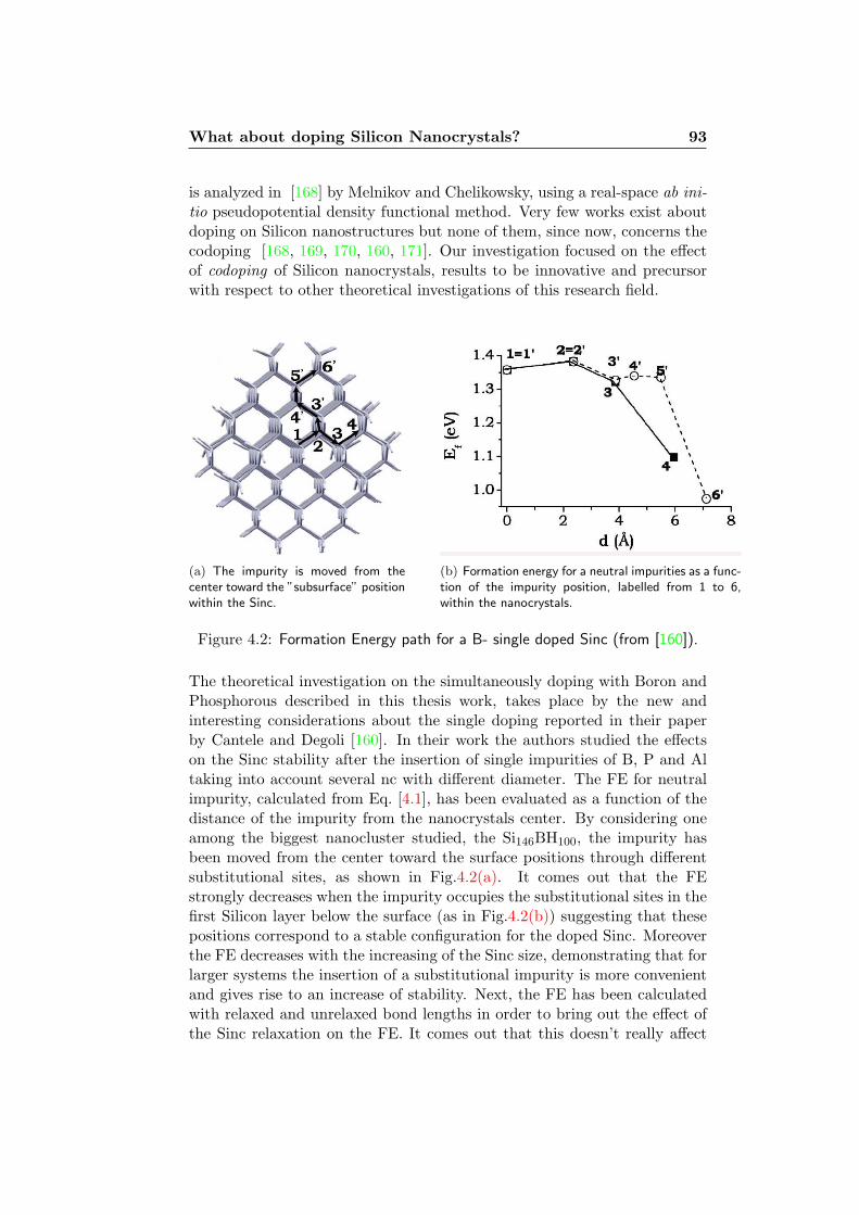
What about doping Silicon Nanocrystals? 93
is analyzed in [168] by Melnikov and Chelikowsky, using a real-space ab ini-tio pseudopotential density functional method. Very few works exist aboutdoping on Silicon nanostructures but none of them, since now, concerns thecodoping [168, 169, 170, 160, 171]. Our investigation focused on the effectof codoping of Silicon nanocrystals, results to be innovative and precursorwith respect to other theoretical investigations of this research field.
(a) The impurity is moved from thecenter toward the ”subsurface” positionwithin the Sinc.
(b) Formation energy for a neutral impurities as a func-tion of the impurity position, labelled from 1 to 6,within the nanocrystals.
Figure 4.2: Formation Energy path for a B- single doped Sinc (from [160]).
The theoretical investigation on the simultaneously doping with Boron andPhosphorous described in this thesis work, takes place by the new andinteresting considerations about the single doping reported in their paperby Cantele and Degoli [160]. In their work the authors studied the effectson the Sinc stability after the insertion of single impurities of B, P and Altaking into account several nc with different diameter. The FE for neutralimpurity, calculated from Eq. [4.1], has been evaluated as a function of thedistance of the impurity from the nanocrystals center. By considering oneamong the biggest nanocluster studied, the Si146BH100, the impurity hasbeen moved from the center toward the surface positions through differentsubstitutional sites, as shown in Fig.4.2(a). It comes out that the FEstrongly decreases when the impurity occupies the substitutional sites in thefirst Silicon layer below the surface (as in Fig.4.2(b)) suggesting that thesepositions correspond to a stable configuration for the doped Sinc. Moreoverthe FE decreases with the increasing of the Sinc size, demonstrating that forlarger systems the insertion of a substitutional impurity is more convenientand gives rise to an increase of stability. Next, the FE has been calculatedwith relaxed and unrelaxed bond lengths in order to bring out the effect ofthe Sinc relaxation on the FE. It comes out that this doesn’t really affect

94 4. The Systems
the stability of the system: the FE still decreases with the increasing ofdimensions maintaining an almost linear scaling while the relaxation justaround the impurity determines a rigid downward shift of FE toward lowerenergy.
Due to these considerations about the single impurity Formation Energyin the paper by Cantele and Degoli [160], we decide to codope the Sincinserting simultaneously the Boron and Phosphorous impurities in the firstSilicon layer below the surface, as shown in Fig. 4.3. In this configuration theimpurities are placed in each Sinc at the largest possible distance accordingto the diameter of the nanocrystals and to the condition to occupy substi-tutional site in the first layer below the hydrogenated surface, as depictedfrom the following resuming Table 4.1:
Diameter DBP
(A) (A)
Si33BPH36 11 3.64Si85BPH76 15 10.60Si145BPH100 17.9 13.59
Table 4.1: Diameter and impurity-impurity distance for the codoped Sinc con-sidered in this work.
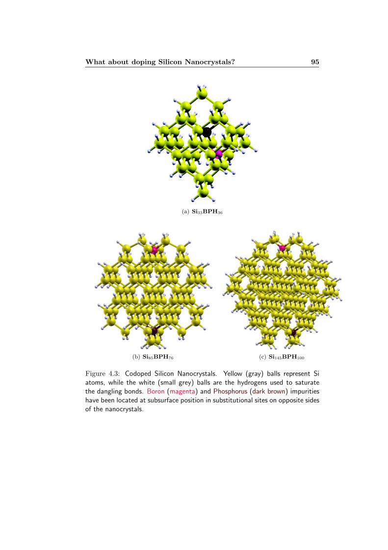
What about doping Silicon Nanocrystals? 95
(a) Si33BPH36
(b) Si85BPH76 (c) Si145BPH100
Figure 4.3: Codoped Silicon Nanocrystals. Yellow (gray) balls represent Siatoms, while the white (small grey) balls are the hydrogens used to saturatethe dangling bonds. Boron (magenta) and Phosphorus (dark brown) impuritieshave been located at subsurface position in substitutional sites on opposite sidesof the nanocrystals.

96 4. The Systems
4.4 Codoping: Structural Properties
In this section we’re going to examine how the structural properties are in-fluenced by the presence of two substitutional impurities with respect to theundoped hydrogenated Sinc and the single doped ones. After the insertionof impurities the Sinc have been relaxed to achieve the most reliable geo-metric configuration corresponding to the absolute minimum of total energy.We observe that the insertion of one and/or two impurities gives rise to
Si87H76 Si86BH76 Si86PH76 Si85BPH76
Bond A Bond A A A
Si-Sis 2.355 B-Sis 2.036 2.021Si-Sis 2.355 B-Sis 2.036 2.021Si-Sii 2.363 B-Sii 2.014 2.034Si-Sii 2.363 B-Sii 2.014 2.034
Si-Sis 2.355 P-Sis 2.294 2.295Si-Sis 2.355 P-Sis 2.294 2.295Si-Sii 2.363 P-Sii 2.380 2.331Si-Sii 2.363 P-Sii 2.380 2.331
Table 4.2: Bond lengths around the impurities site for the undoped Si87H76
nanocrystals and the single- and codoped ones (diameter 1.50 nm). B and Pimpurities have been substitutionally located at subsurface positions (see Fig.4.3(b)). Sis and Sii refer to two surface and two inner Si atoms around this siterespectively.
variations in the bond lengths focalized in particular around the impuritysites, involving in particular the impurity-Si bonds. In Table 4.2, Table 4.3and Table 4.4, are reported the relaxed bond lengths around the impuritiesfor each of the Sinc, Si33BPH36 , Si85BPH76 , Si145BPH100 . Comparing thebond lengths of the single doped nc with those of the undoped one, we cansee from Table 4.2, that the insertion of one impurity in the singled dopednc, determines an important structural relaxation around the impurity site:the initial Td symmetry (ref. to Sec. 4.1) of the undoped Sinc turns intothe C2v symmetry. More specifically this leads to a local structure with twoshorter and two longer Si-impurity distances with respect to the two surfaceand two inner Si atoms. The more significant relaxation with respect tothe undoped nanocrystals is found for the single trivalent atom (B, 2.036A and 2.014 A with respect to 2.355 A and 2.363 A) than for the singlepentavalent one (P, 2.294 A and 2.380 A with respect to 2.355 A and 2.363A). The amount of relaxation around the impurity sites is directly related

Codoping: Structural Properties 97
Si35H36 Si34BH36 Si34PH36 Si33BPH36
Bond A Bond A A A
Si-Sis 2.300 B-Sis 2.093 2.035Si-Sis 2.300 B-Sis 2.022 2.026Si-Sis 2.300 B-Sis 2.022 2.026Si-Sii 2.361 B-Sii 2.008 2.007
Si-Sis 2.300 P-Sis 2.366 2.303Si-Sis 2.300 P-Sis 2.365 2.302Si-Sis 2.300 P-Sis 2.364 2.297Si-Sii 2.361 P-Sii 2.310 2.334
Table 4.3: Bond lengths around the impurities site for the undoped Si35H36
nanocrystals and the single- and codoped ones (diameter d= 1.10 nm). Band P impurities have been substitutionally located at subsurface positions (seeFig. 4.3(a)). Sis and Sii refer to three surface and one inner Si atoms aroundthis site respectively.
to the impurity valence.
For what concerns the codoping, instead, one can see from the same tables,that the differences among the four impurity-Si bond lengths are smallerwith respect to the single-doped case (the Si-B bonds differ of about 1.08%in the single-doped case and only 0.64% in the co-doped case, whereas thisvariation in the case of P reduces from 3.61% to 1.54%). Thus, if carriersin the Sinc are perfectly compensated by simultaneously n- and p-type im-purities doping, an almost Td configuration, in which the four impurity-Sibonds are practically the same, is recovered. Moreover looking at Table 4.3and Table 4.4 where are reported the bond lengths for the Si33BPH36 andSi145BPH100 respectively, one can see that a lowering of the symmetrywith respect to the Si87H76 -based nanocrystals occurs for the smaller andlarger nanoclusters. In this two cases the impurity-Si bond lengths presenta differ trend with respect to the Si85BPH76 : there are now two shorterbonds with the same value, one longer and one with another little differentvalue. In spite of these light structural modifications occurring around theimpurity sites, the possibility to achieve the Td symmetry for codoped com-pensated Sinc is achieved also for the smaller and the larger nanocrystals,demonstrating that this behaviour is independent of the Sinc size. The dif-ferent relaxation trend in the two nanocrystals among the Si-B and Si-Pbond lengths, leading to the lowering of symmetry, can be related to thedifferent Silicon neighborhood experienced by the impurities. In the case ofSi35H36 (blowup in Fig. 4.4) and Si145BPH100 (blowup in Fig. 4.5), the im-

98 4. The Systems
Si147H100 Si146BH100 Si146PH100 Si145BPH100
Bond A Bond A A A
Si-Sis 2.356 B-Sis 2.029 2.016Si-Sis 2.356 B-Sis 2.029 2.016Si-Sis 2.356 B-Sis 2.063 2.018Si-Sii 2.369 B-Sii 2.009 2.022
Si-Sis 2.356 P-Sis 2.310 2.306Si-Sis 2.356 P-Sis 2.310 2.306Si-Sis 2.356 P-Sis 2.372 2.338Si-Sii 2.369 P-Sii 2.321 2.321
Table 4.4: Bond lengths around the impurities site for the undoped Si147H100
nanocrystals and the single- and codoped ones (diameter d = 1.79 nm). B andP impurities have been substitutionally located at subsurface positions (see Fig.4.3(c)). Sis and Sii refer to three surface and one inner Si atoms around thissite respectively.
purities in the first layer below the surface are bonded to one inner Si atomand to three surface Si atoms passivated with one and two hydrogen whilein Si85BPH76 the impurities have two surface Si atoms and two inner coreSi neighbors (see blowup in Fig. 4.5): to that the impurity sites experiencea different relaxation, with a different amount of bond softening.
After the investigation on the effect of dimension and chemistry on thestructural relaxation, we focus the attention on the effect played by theimpurity-impurity distance on the structural modification when two impu-rities are simultaneously present in the same nanocluster, comparing theimpurity-Si distances to the corresponding Si-Si ones for the undoped nc.We consider the biggest nanocrystals reported here, the Si147H100 , and bykeeping fixed the Boron in a subsurface position, we moved the Phospho-rus through substitutional sites all along the first subsurface Silicon layer,as schematically depicted in Fig. 4.6. For each of the impurity sites occu-pied by the Phosphorous and labelled by position by II, III, V-a, V-b, VI-a,VI-b, VIII-a, VIII-b, IX-a, IX-b and X, where the roman number refers sim-ply to the positions evidenced in Fig. 4.6, a different configuration has beenachieved and for each of them energy and structural minimization have beenperformed through ab initio calculations. Then, for each minimized config-uration, the relaxed B-P and the corresponding Si-Si distances have beencalculated. These values are reported in Fig.4.7 where are also comparedwith the corresponding relaxed Si-Si distances of a 6 × 6 × 6 supercell bulk

Codoping: Structural Properties 99
Figure 4.4: Blow up of the bond lengths around the impurity sites in codopedSi33BPH36 . The ”S” label indicates surface Silicon atoms bonded to the impu-rity, while the ”i”refers to the inner Si atoms. In yellow are Si atoms, in whitethe H ones at surface.

100 4. The Systems
Figure 4.5: Blow up of the bond lengths around the impurity sites in codopedSi145BPH100 (left side) and Si85BPH76 (right side). The ”S” label indicatessurface Silicon atoms bonded to the impurity, while the ”i”refers to the inner Siatoms. In yellow are Si atoms, in white the H ones at surface.

Codoping: Structural Properties 101
Figure 4.6: ”Phosphorus impurity path” in Si145BPH100. Phosphorus atom(dark brown) exploring several substitutional sites (labelled by number) whileBoron atom (magenta) fixed: both atoms are in first Si layer below the surfaceshell.

102 4. The Systems
Figure 4.7: Boron-Phosphorus substitutional site distances in the Si145BPH100
nanocrystal (blue circles) and the corresponding Si-Si distances in the undopedSi147H100 nanocrystal (cyan squares) compared to the bulk Silicon correspondingdistances (red diamonds).
Silicon. Since the bulk Silicon distances are considered as reference, valuesabove the dashed line correspond to an increase of the B-P distance, whilevalues below correspond to a reduction. Thus, since the displacement of theB-P distance values with respect to this line is really small, one can concludethat only weak modification occur in the codoped distances with respect tothe bulk. On going from the undoped nanocrystals, where the distances arepractically the same as in bulk Silicon, to the codoped ones we note a verysmall shrinkage of the impurity-impurity distances with respect to the pre-vious Si-Si distances. This shows, once again, that if carriers in the Sinc areperfectly compensated by simultaneous doping, the starting undoped Sincundergoes practically no geometry distortion. In Table 4.5 are resumed therelaxed B-P distances for the codoped Sinc of different dimensions consid-ered here.

Codoping: Formation Energy 103
Cluster B-P Distance Neighbors index(A)
Si33BPH36
B,P @I shell 3.5646 2nd
Si85BPH76
- B,P @ I shell (1) 10.5940 VIII
Si145BPH100
B,P @I shell13,594 X13.286 IXb
12,2022 IXa
11,9254 VIIIb11,3159 VIb11,2973 VIIIa9,9503 VIa7,9056 Vb
6,9328 Va
4,3970 III3.68 II
Table 4.5: Relaxed B-P distances for codoped Sinc.
4.5 Codoping: Formation Energy
The structural modifications introduced by the presence of one or two impu-rities discussed in the previous section, affect also the stability of the systemand have to be carefully taken into account when dealing with different kindof single and co- doped Silicon nanocrystals. The stability of doped systemshas been evaluated through the calculation of the Formation Energy (FE),defined in Sec. 4.2, as the energy required to insert neutral impurities ofB or/and P substitutionally within the hydrogenated Silicon nanocrystalsSinHm [44] by removing an equivalent number of Si atoms, and depicted inEq. [4.1]. In order to clarify which are the parameters that play a crucial rolein the determination of the Formation Energy, we have performed a seriesof total energy calculations considering: i) single-doped and codoped nano-crystals, ii) nanocrystals of different sizes, iii) impurities located in differentsites and iv) variable impurity-impurity distance within the same nanocrys-tal. First of all our aim is to understand which kind of doping is more easierto realize, by comparing in Fig.4.8 FE for B and P single and co- doped Sinc,for each size of Sinc considered here. To note that in this figure the B and Pimpurities have been placed in the Sinc as second neighbors, since this choice
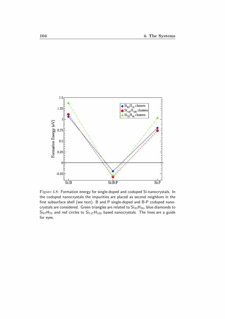
104 4. The Systems
Figure 4.8: Formation energy for single-doped and codoped Si-nanocrystals. Inthe codoped nanocrystals the impurities are placed as second neighbors in thefirst subsurface shell (see text). B and P single-doped and B-P codoped nano-crystals are considered. Green triangles are related to Si35H36, blue diamonds toSi87H76 and red circles to Si147H100 based nanocrystals. The lines are a guidefor eyes.

Codoping: Formation Energy 105
corresponds to the nearest possible distance between the two impurities forthe Si33BPH36-nc in Fig. 4.3(a), and the Si145BPH100-nc (see the positionlabelled II in Fig. 4.6). After geometry relaxation the distances between Band P impurities are DBP = 3.56 A, DBP = 3.64 A and DBP = 3.68 A forthe Si33BPH36, Si85BPH76 and Si145BPH100 nanocrystals, respectively, asshown in Table 4.5.From Fig. 4.8 it is clear that simultaneous B and P doping strongly reduces(of about 1 eV) the Formation Energy with respect to both B or P single-doped cases and that this reduction is similar for Sinc of different size. Thuswhile B or P single doping is very costly (in particular, the formation energyincreases with decreasing nanocrystals size, in agreement with previous cal-culations [168, 160]) B and P codoping results much easier to obtain andalmost independent on the nanocrystals size. The important point here isthat Sinc can be more easily simultaneously doped than single-doped; this isdue to both the charge compensation and the minor structural deformationsubdue by the Sinc.Moreover we performed more calculations exploring different configurationof codoped impurities, in order to investigate in details the dependenceof FE on the distance between impurities and on the Sinc dimension. InFig. 4.9 has been compared the FE for the single and co- doped Si87H76 andSi147H100 nanocrystals with impurities placed at two different distances:first the impurities are second neighbors in both the nc (as in previousFig. 4.8), the minimum possible distance considering only substitutionalsubsurface position (relaxed DBP =3.64 A and 3.68 A respectively) andthen the impurities are placed at the largest possible distance accordingto the dimension of the Sinc, that means after the relaxation, DBP =10.60A for Si85BPH76 and DBP =13.29 A for Si145BPH100 respectively. It’sworth pointing out that for both the nanocrystals considered when theimpurity-impurity distance is reduced, the Formation Energy decreases of0.2-0.3 eV and assumes negative values. This fact demonstrates that astronger interaction between n- and p- type impurities leads to a strongreduction in the Formation Energy, so that codoping results easier to realizewhen the dopants are closer each other. The amount of Formation Energyreduction is about the same for each considered nanocrystals, and thus, asshown in Fig. 4.8, it’s almost independent by the nanocrystals size. Sincethe FE used here is calculated as a difference between the total energies ofthe nanocrystals with and without impurities (see Eq.[ 4.1], negative valuesof FE obtained for the codoped Sinc in Fig. 4.9 means that the calculatedtotal energies of the codoped nanocrystals are bigger in absolute valuethan the total energies of the single doped nc. More negative are theseFE values, more the codoped nanocrystals are likely to be obtained duringthe formation process with respect the single doped ones under the samegrowth conditions.

106 4. The Systems
Figure 4.9: Formation Energy of Si87H76 and Si147H100 single-doped andcodoped nanocrystals, with impurities placed within the codoped nanocrystalsat two different distances: a large (dashed lines) and a small one (solid lines)(see text). Red circles refer to Si87H76-nc and blue squares to Si147H100-nc.The lines are a guide for eyes.
Nonetheless, regarding again Fig. 4.8, it comes out that the smallest B- andP- single doped nc, the Si34PH36 and Si34BH36 , present the greater positiveFE values with respect to the other single doped cases. This suggests thatthe single doping in small clusters results to be more difficult to realize andmore unfavorable than in other cases. This aspect is in good accord withthe conclusion asserted by Dalpian and Chelikowsky [161]: the increase inthe formation energies of these impurities with the decrease of the nc size isa clear evidence that single doping small nanocrystals is more difficult com-pared to single doping bigger systems, such as bulk for example. Dalpianand Chelikowsky define self-purification a possible intrinsic property of na-nocrystals, consisting in the exclusion of dopants from small nanocrystals,that follows the increase of Formation Energy. This confirms the fact thatsubstitutional impurities are more stable in subsurface position just below

Codoping: Formation Energy 107
the surface, contributing then to shed more light on the most preferred po-sition of single dopants within the nanocrystals. From the experimentalworks, the doped and codoped Sinc are described such as embedded in anglass Boron and/or Phospho- silicate glass matrix. One possible hypothesisone the location of impurities is that the dopants could prefer to migrate atthe interface between the nanocrystals and the silica matrix, according tothe intrinsic difficulty of impurities to diffuse into small Sinc, that thereforeconstrains the impurities to be relegate in the interface region. The nanocry-stals dimensions can be an important parameter to manage with the dopingprocess like the structural modifications which can also affect the stabilityof the system as demonstrated by the work of Ramos et al. [169, 170] wherethe FE of single doped impurities strongly varies by moving from sphericalto faceted Sinc.Nevertheless, our investigation on the codoping Sinc, demonstrates how thesimultaneous insertion of donor and acceptor impurities within Sinc is moresuitable than single doping, and that the amount of reduction of FE is prac-tically size independent; although only spherical Sinc are here considered,we can think concerning the codoping that the faceted Sinc present a similarbehaviour in which the size and shape have assume reduce importance withrespect to the singled doped cases studied in [170].Then, in order to investigate more in details the dependence of the For-mation Energy on the impurity-impurity distance, we focus our attentionon the biggest codoped Si145BPH100, trying to trace a ”Formation Energypath” by progressively increasing the B-P distance. To do this we keptfixed the B atom in a subsurface position and moved the P atom throughdifferent substitutional site along the first subsurface shell, as schematicshown in Fig. 4.6 and already explained in the previous Section 4.4. Foreach different configuration, we performed total energy DFT calculationin order to evaluate opto-electronic properties and Formation Energy as afunction of the B-P distance within the nanocrystal.
The results of these calculations are shown in Fig. 4.10 and Fig. 4.11 wheretwo interesting effects are evidenced. From Fig. 4.10 we observe an aug-mentation in FE with the increase of the Boron-Phosphorus distance withinthe nanocrystal, as depicted in Fig. 4.10, where is reported the FE for eachof the different impurity configuration as a function of the B-P distance interms of the distance (in Angstrom) and of the neighbors site index labelledin Roman numbers. Some interesting consideration could be done.The first is that FE assumes negative values for impurity between the site II(3.68 A) and site VI (9.95 A) while going up with the distance, FE becomesbigger and positive. This change from negative to positive values, can leadto the definition of a ”critical impurity distance”: below such value, theinteraction between Boron and Phosphorus is stronger and it gives rise to areduction of FE meaning that codoping results more favorable and increase

108 4. The Systems
the stability of Sinc, while, above this value, the Coulomb interaction tendsto be more screened and therefore to be quenched leading to a minor influ-ence on the FE then reducing the stability of the impurity complex withinthe nanocrystals.
Figure 4.10: Formation Energy as a function of the Boron-Phosphorus distance.Roman numbers refer to the positions of the P atom (see Fig. 4.6). The dottedand dashed lines connect two categories of impurity sites, where the surroundingsurface Si atoms are bounded to the same number of passivating H atoms.
These outcomes are supported also by Fig. 4.11, in which we report thevalues of the Formation Energy for three nanocrystals different in sizeand with impurities located in the subsurface shells at different distances.As before, it appears clear that the distance between impurities plays afundamental role on the decrease of the Formation Energy. Below a givenimpurity-impurity distance the Formation Energy assumes negative valuesfor each nc size. Moreover we see that the Formation Energy shows theminimum value when the impurities are located at the minimum possibledistance in each codoped Sinc apart from the different diameter size.Indeed the impurity-impurity distance seems to play a major role on theFE with respect to the nanocrystals size, since the Formation Energyvalues are similar for similar impurity-impurity distances independently ofthe nanocrystals dimension. The small difference between the Si85BPH76 ,the Si33BPH36 and the Si145BPH100 is due to the different neighborhood

Codoping: Formation Energy 109
Figure 4.11: Formation Energy as a function of Sinc size and impurity-impuritydistance. For the three different considered Sinc one has the following nc diam-eters (d) and impurity-impurity distances (DBP): Si33BPH36 d= 1.10 nm andDBP = 3.56 A (site II); Si85BPH76 d= 1.50 nm and DBP = 2.00 A (site I), DBP
= 3.64 A (site II), DBP = 10.60 A (site VIII); Si145BPH100 d= 1.79 nm andDBP = 3.68 A (site II), DBP = 4.40 A (site III), DBP = 6.93 A (site V-a), DBP
= 7.91 A (site V-b), DBP = 9.95 A (site VI-a), DBP = 11.32 A (site VI-b),DBP = 11.30 A (site VIII-a), DBP = 11.93 A (site VIII-b), DBP = 12.20 A (siteIX-a),DBP = 13.29 A (site IX-b), DBP = 13.59 A (site X).
experienced by the impurities in the three cases (see Tables I, II and III).
The second other relevant point is the possibility to identify two distincttrends for the Formation Energy depicted in Fig. 4.10, that can be relatedto the type of Silicon cage surrounding the P dopant site. One can group(dotted line) together the cases in which the P impurity is located in thepositions labelled II, VI-b and X with respect to the B impurity (see Fig.4.6). In these positions two of the surface Si atoms bounded to the Pimpurity present two passivating H atoms instead of one, the situationthat actually dominates in all other configurations; it’s thus possible to saythat a different number of capping H atoms influences the Formation Energy.

110 4. The Systems
Many other calculations has been done on the biggest Si145BPH100 codopednanocrystals with impurities located at the center of the nanocrystals inorder to shed more lights on the most favorable dopants sites. Different Band P impurity configurations have been investigated taking into accountcases with impurities placed like near neighbors and second neighbors atthe center of the nc. It comes out that the inner substitutional sites arenot among the most stable positions for impurities, since they give rise topositive Formation Energy values: near neighbors B-P impurities give a FEequals to 0.18 eV, while when B and P are second neighbors the FE decreasesa little bit but still remaining positive around 0.08 eV. Moreover when theP is located at the center of the nc while the B is substituted in the firstsubsurface layer the FE diminishes again at the value of 0.018 eV, close tozero but positive, confirming once again that the most favorite positions forboth Boron and Phosphorus are the subsurface sites.

5Back to the future:
OptoElectronics
Son morto con altri cento,son morto ch’ero bambinopassato per il camino,e adesso sono nel vento.
Auschwitz, Francesco Guccini
In this new section we present the calculated optoelectronic features of theB and P codoped Silicon nanocrystals. The aim is to understand the roleplayed by the simultaneously presence of substitutional acceptor and donorimpurities such as Boron and Phosphorous , on the electronic structureof the nanocrystals and to investigate how this features can be manipulatedand engineered by simply handling with impurity position within the system.As already depicted in the Introduction, the main goal of this research wouldbe the full comprehension of the mechanism that rule the emission and thetuning of visible light from the doped and codoped Sinc, yet experimentallyobserved by the group of Minoru Fujii. From the theoretical point of viewthis will contribute enormously to the research on Silicon nanocrystals forphotonic applications.
5.1 Electronic Properties
Here, as the title preventively suggests, are described the electronic proper-ties of the single and co- doped Sinc. The semiconductors doping is nowa-days a well established technique used to inject and manage the numbersof carriers in semiconductors systems, or to shift insulator system into se-miconductors through the insertion of donor and/or acceptor impurities. It
111

112 5. Back to the future: OptoElectronics
has been proof that when impurities are present or later inserted in semi-conductors, new discrete electronic levels arise due to the impurities withinthe band gap [172]. The dopants are classified by their chemical valence.In particular, in the tetrahedral elemental semiconductor, impurities withvalence charge greater than four are considered as donors (like elementsfrom V group, P, As, N) while impurities with valence lower than four arecalled acceptors, such as the elements from III group like B, Al. This iswhat happens also in Silicon, the most popular semiconductor among thetetravalent ones, as depicted by Fig. 5.1. The donors dopants posses anextra electron which doesn’t participate to the chemical tetravalent bond-ing and it’s relatively free to move throughout the crystal. On the otherhand, the acceptors atoms, need an extra electron to complete the tetrava-lent coordinate bonding of the elemental crystalline environment; thus theunsaturated bond may migrate throughout the crystal and in this way it canbe depicted as an hole. The semiconductors with an insignificant number of
Figure 5.1: Chemical valence of the dopants inserted into a tetrahedral semi-conductor, here bulk Silicon. Atoms from III group like Boron become acceptors
while atoms from V group, such as Phosphorus, are defined as donors.
carriers can be consider almost pure and are called intrinsic. The number ofcharge carriers is therefore determined by the properties of the material itselfinstead of the amount of impurities; moreover in intrinsic semiconductorsthe number of electrons and the number of holes are equal. Instead, whenan amount of dopants impurities is inserted into a semiconductor, whichresults to be doped, the semiconductor is called extrinsic. The electron andhole carrier concentrations of the semiconductor at thermal equilibrium arethen changed. Dominant carrier concentrations in an extrinsic semiconduc-tor classify it as either an n-type or p-type semiconductor. The electricalproperties of extrinsic semiconductors make them essential components ofmany electronic devices. The donor and acceptor impurities considered hereare called shallow since they give rise to discrete energy level close to the

Electronic Properties 113
conduction and valence band edge respectively as shown in Fig. 5.2.
Figure 5.2: Energy levels of acceptors and donors in the semiconductor banddiagram, placed near the conduction EC and valence EV band edge. The shal-low donor energy level ED and the acceptor energy level EA have respectivelyionization energies Ed and Ea.
The main idea behind this work is to demonstrate from a theoreti-cal point of view but supported by the experimental evidences (seeFujii[41, 33, 36, 40, 32, 38]) that the traditional doping of bulk semicon-ductor can be also applied to nanostructured system in order to controlnot only electrical properties but especially the optical features of theseinnovative systems. The possibility to achieve visible light and to tune itsspectrum just playing with the doping of the Sinc represents a new andgroundbreaking combination of a traditional well established techniquewith one of the newest class of nanosized system which should be stilldeeply investigate at all.
Free standing undoped hydrogenated Silicon nanocrystals show an electronicstructure constituted by discrete energy levels as a consequence of the quan-tum confinement effect, as demonstrated by numerous works realized inthe last 15 years [51, 173, 117, 174, 47, 44]. The undoped Sinc have asemiconductor-like band gap that varies according to the variations of thedimensions of the nanocrystals. The introduction of dopant atoms withinthe Silicon nanocrystals has been demonstrated to produce a behaviour sim-ilar to the doping bulk semiconductor, with the creation of discrete impuritystates near the conduction and valence band edge.

114 5. Back to the future: OptoElectronics
B, P Single doped Nanocrystals
All the data regarding the electronic structures calculated are obtained, asfor the geometric structure, using Vanderbilt ultrasoft pseudopotential withGGA exchange-correlation functional.First of all we’re going to resume what happens when only one impurity(Boron or Phosphorous ) is present within the Sinc. In Fig. 5.3 and inFig 5.4 are reported the energy levels calculated at Γ for the two differentsize of Sinc; only the levels corresponding to the highest occupied molec-ular orbital (HOMO), the lowest unoccupied molecular orbital (LUMO),the HOMO-1 and LUMO+1 states are shown. According to the previousconsiderations about the formation energy and thus on the more preferredimpurity position within the Sinc, here the impurities are single doped inthe first layer below the surface, as one can see from Fig.5.5 where the lo-calization of HOMO and LUMO states is shown. As for bulk Silicon, theimpurities inserted give rise to new shallow electronic levels near the bandedge. The Boron dopant gives rise to an impurity level close the valenceedge, while the Phosphorous atom gives rise to a level localize just be-low the conduction band edge. As reported in Fig. 5.3 and Fig. 5.4 theseKohn-Sham impurity levels become more shallow as the size of Sinc increase,thus when the quantum confinement is reduced and the dimensions tend tothe bulk limit. The HOMO (Highest Occupied Molecular Orbital) level of
Figure 5.3: Calculated energy levels at the Γ point for the Si35H36 , theSi34BH36 and Si34PH36 single doped Sinc. The alignment has been performedlocating at the same energy the fully occupied levels with the same type oflocalization.
single doped nanocrystals contains only one electron and the Kohn-Sham

Electronic Properties 115
energy gap is defined for the single doped nc as the energy difference be-tween the highest occupied level (HOMO) that is partially filled and thelowest unoccupied one (LUMO) which is empty. The presence of donor oracceptor states lowers the above defined energy gap (EG) with respect thecorresponding undoped Sinc and the changes in the electronic structure aredirectly related to the impurity valence. Since the impurity level is semi-occupied it leads the single doped Sinc to have an odd numbers of electronswith respect the undoped ones and to become a metallic system. Performingspin-polarized calculations it has been demonstrated that the impurity levelwith the lower energy is always occupied by the unpaired electron (spin-upor spin-down) while the level with higher energy is not occupied [170]. Some
Figure 5.4: Calculated energy levels at the Γ point for the Si87H76 , theSi86BH76 and Si86PH76 single doped Sinc. The alignment has been performedlocating at the same energy the fully occupied levels with the same type oflocalization
light differences arise between spin-up and spin-down energy calculations,and in particular the amount of discrepancy between spin-up and spin-downstates depends slightly by the Sinc size: for small nc the splitting is morepronounced while for bigger the differences tend to become negligible [170].Nonetheless the actual calculations on the B and P singled doped Sinc arein fair good agreement with other similar investigation on the single dopingSinc made by Zhou and Brus [171, 175].
The insertion of a single impurity into the nc perturbs then not only theelectronic structure, but also the localization of the HOMO and LUMOorbitals of the Sinc, with respect to the undoped counterpart, as depicted

116 5. Back to the future: OptoElectronics
in Fig. 5.5. The HOMO and LUMO orbitals of the undoped Sinc are spreadall over the entire cluster, as confirmed by previous work on hydrogenatednanocrystals[44]; in the single doped cases, instead, the HOMO is stronglyfocused on the Boron and Phosphorous impurity sites, while the LUMOis delocalized over the all Silicon inner core of the nc, thus recovering thetypical behaviour of the undoped hydrogenated Sinc. Due to the stronglocalization of the impurity level, for example, in the case of Si86BH76 thedefect level is located just 0.28 eV above the valence band reducing theabove defined energy gap from 2.59 eV (the value for the undoped Sinc)to 2.31 eV. In Si86PH76 the defect level is located just 0.28 eV below theconduction band so that the energy gap is only 0.28 eV. It is interesting tonote that the experimental substitutional donor binding energy for P in bulkSi is about 33 meV, while the experimental acceptor energy for B in Si is 45meV,[176] showing how, in the case of nanocrystals, the combined effects ofboth quantum confinement and weak screening tend to “transform” shallowimpurities in “deep” centers [168, 160, 177].

Electronic Properties 117
Figure 5.5: The HOMO (left column) and LUMO (right column) square mod-ulus contour plots calculated for the B and P single doped Si35H36- (upperpanel) and Si87H76- (lower panel) based nc.The isosurfaces correspond to 10%of the maximum value.

118 5. Back to the future: OptoElectronics
B and P Codoped Nanocrystals
When the Boron and Phosphorous dopant atoms are simultaneously in-serted within the Sinc, the single perturbations related to the presence ofan acceptor and a donor impurity sum and the system recover a semicon-ductor character. It means that new electronic levels due to the simul-taneous codoping and related to the different character of the III and Vgroup dopants, arise into the energy gap of the Sinc which is fully occupied.This can be clarified from Fig. 5.6 where we show the electronic levels for
Figure 5.6: Calculated energy levels at the Γ point for the Si87H76 , Si86BH76 ,Si86PH76 and Si85BPH76 nc. The alignment has been performed locating atthe same energy the fully occupied levels with the same type of localization.
the Si87H76- based nc, the single doped (as in the previous section) andthe codoped Si85BPH76. Again only the HOMO, LUMO, HOMO-1 andLUMO+1 orbital states are reported (see Fig. 5.7) and the alignment hasbeen realized locating at the same energy the states with the same kind ofelectronic occupations and with the same type of localization. It comes outthat now on going from the pure to the codoped nc, the HOMO and LUMOstates tend progressively to localize around the two impurity sites (bottompanel of Fig. 5.7): thus the HOMO is mainly focused around the Boronimpurity, the acceptor, while the LUMO is centered around the Phosphorusimpurity, the donor site. Thus we can associate HOMO and LUMO statesto the new impurity levels, and we have to remember that the codoped ncwe’re dealing is compensated by the presence of a donor and an acceptor

Electronic Properties 119
at the same time, with valence levels completely double occupied. The newHOMO and LUMO impurity states arise within the energy gap, determininga strong reduction from 2.5867 eV (undoped Sinc) to 1.8228 eV (codopedSinc).
The same trend is realized for the codoped Si33BPH36 with respect to theSi35H36, where the energy gap of the codoped Sinc is strongly reduced byan amount of about 1 eV as depicted in Fig. 5.8 where energy levels at Γare depicted for the smallest single and codoped nc.
It worth pointing out how the distance between the two impurities withinthe Sinc could influence the electronic structure. Thus on going from thesmallest to the biggest nanocrystals we decide to investigate the electronicproperties as a function of the impurity-impurity distance. Several config-urations of codoped nc with coupled impurities inserted in the first Siliconlayer below the surface (following the consideration on the FE of the pre-vious section) with different distance between the Boron and the Phos-phorous atoms have been investigate. To better understand how the B-Pdistance could really influence the electronic properties, we take into accountone of the biggest Sinc, the Si145BPH100 codoped with the impurities placedone time at the largest possible distance in the first subsurface Silicon layer(DBP=13.29 A) and the second time at the lowest possible distance suchas second neighbors just below the surface (DBP=3.69 A) and then we cal-culate the corresponding electronic structures as shown in Fig. 5.9. Fromthe figure it comes out that when the two impurities are at the larger dis-tance (corresponding to site X) the energy gap EG is strongly lowered withrespect to the undoped Si147H100 moving from 2.30 eV to 1.63 eV; moreoverwhen the impurities are closer each other, thus second neighbors (configu-ration labelled by site II), the EG enlarges to 2.03 eV, keeping always lowerthan the value of the undoped Sinc. A possible explanation is that whenimpurities are brought closer each other, the Coulomb interaction becomesstronger so that the energy gap becomes larger. Boron and Phosphorus feeleach other like a B-P complexes with a gap opening recalling the DFT-LDAcalculated gaps for the Boron Phosphide bulk system: direct gap ( Γ → Γ )3.3 eV, indirect gaps ( Γ → X ) 2.2 eV, and ( Γ → ∆ ) 1.2 eV, as describedin [178]. These behaviors are corroborated by the calculated HOMO andLUMO wave functions. Fig. 5.10 shows the square modulus contour plots ofthe HOMO and LUMO states of the two Si145BPH100 nanocrystals with dif-ferent B-P distances. The top panel shows the contour when the impuritiesare at a large distance while the bottom panel is that with the impuritiesat short distance. It clearly appears from these contours that on going fromthe case with well separated impurities to the that with close impurities, theoverlap between the HOMO, strongly centered on the Boron atom, and theLUMO, mainly localized on the Phosphorus atom, strongly increases.
Moreover, the detailed influence played by the mutual B-P distance onthe electronic structure of codoped Sinc, has been carried out by looking at

120 5. Back to the future: OptoElectronics
Figure 5.7: The HOMO (left column) and LUMO (right column) square mod-ulus contour plots calculated for the Si86BH76 (top panel), Si86PH76 (middlepanel) and Si85BPH76 (bottom panel). The isosurfaces correspond to 10% ofthe maximum value
the changes in the electronic levels for each of the impurities configurations

Electronic Properties 121
Figure 5.8: Calculated energy levels at the Γ point for the Si33BPH36 ,Si34BH36 , Si34PH36 and Si35H36 nc. The alignment has been performed locat-ing at the same energy the fully occupied levels with the same type of localiza-tion.
within the Si145BPH100 nanocrystal (see Fig. 4.6) as done before for theformation energy. In Fig. 5.11, the trend of the HOMO-LUMO energygap with respect to distance between impurities within the Si145BPH100 isreported. What comes out is that the mutual impurity distance deeplyaffects not only the formation energy (as in Sec. 4.2) but also the energy gapof the semiconductor nanocrystals. As one can see, the EG strongly decreasesalmost linearly with the increase of the impurity distance; moreover, also inthis case we can figure out the presence of two different trends related to thedifferent surface region experienced by the P atom in the sites II, VI-b andX, with respect to the other ones (see also Fig. 4.10 and related discussion).Fig. 5.11 points out how, at least in principle, it is possible to tune EG asa function of the impurity-impurity distance. It is easy to predict that forSinc larger than those considered here it would be possible by codoping toobtain a energy gap even smaller than whose of bulk Si.
Moreover, by keeping constant the impurity-impurity distance between Band P for each dimension of the Sinc considered, it’s possible to see how theenergy gap depends by the Sinc size. By placing the B and P impuritieslike second neighbors in substitutional subsurface position in all the differentSinc, it come out how its in principle possible to tune and modulate the elec-tronic gap by moving from the undoped to the codoped Sinc. From Fig. 5.12it can be see how the undoped EG is strongly reduced in the presence ofcodoping. In particular also looking at the numerical values in Table 5.1,

122 5. Back to the future: OptoElectronics
Figure 5.9: Calculated energy levels of the undoped Si147H100 (left panel),codoped Si145BPH100 with an impurity-impurity distance DBP = 13.29 A (cen-tral panel), codoped Si145BPH100 with an impurity-impurity distance DBP =3.68 A (right panel). The alignment has been done locating at the same energythe fully occupied levels with the same type of localization. Site X and Site IIare referred to Fig. 4.6. H stands for HOMO, L for LUMO.
the EG of the codoped Sinc appear to be shifted toward lower values withrespect to the corresponding undoped ones. The amount of shift is strongerfor smaller nanocrystals, 0.65 eV for Si33BPH36 , 0.30 eV for Si85BPH76 and0.27 eV for Si145BPH100, but it tends to saturate when the diameter of theSinc exceeds some threshold value (here the Si87H76diameter). The samequantum confinement effect trend (i.e. larger gap for smaller nanocrystals)is observed for both the undoped and the codoped cases. The energy gaptrend depicted in Fig. 5.11 and Fig. 5.12 can be directly connected withthe experimental outcomes by Fujii and coworkers [38, 36, 37] who foundphotoluminescence peaks centered in the 0.9-1.3 eV energy region: we cantherefore argue that Sinc playing a role in the experiment should have di-mensions of the order of few nanometers, as shown from the EG decreasingtrend in Fig. 5.11. This foregone conclusion is consistent with the experi-mental outcomes [38, 36, 37] that indicates an average nanocrystals diameterof about 5 nm. The possibility to modulate and control at pleasure the elec-tronic structure, in particular the possibility to tune the energy gap of theSinc just by the modulation of codoping, discloses several new routes forelectronic and optoelectronic applications.

Electronic Properties 123
(a)
(b)
HOMO LUMO
Figure 5.10: From the top to the bottom: the HOMO (left) and LUMO (right)square modulus contour plots calculated for Si145BPH100 (atom colors same asin Fig. 4.3). The impurities are located on opposite sides of the nanocrystal, atdistance DBP = 13.29 A (a) or as second neighbors, with an impurity-impuritydistance DBP = 3.68 A(b). The isosurfaces correspond to 10% of the maximumvalue.

124 5. Back to the future: OptoElectronics
Figure 5.11: The HOMO-LUMO energy gap as a function of the distancebetween the B and P impurities within the Si145BPH100 nc. Roman numbersrefer to the positions of the P atom (see Fig. 4.6). The dashed and dash-dottedlines connect the two subsets of impurity sites in which the surrounding surfaceSi atoms are bonded to the same number of passivating H atoms.
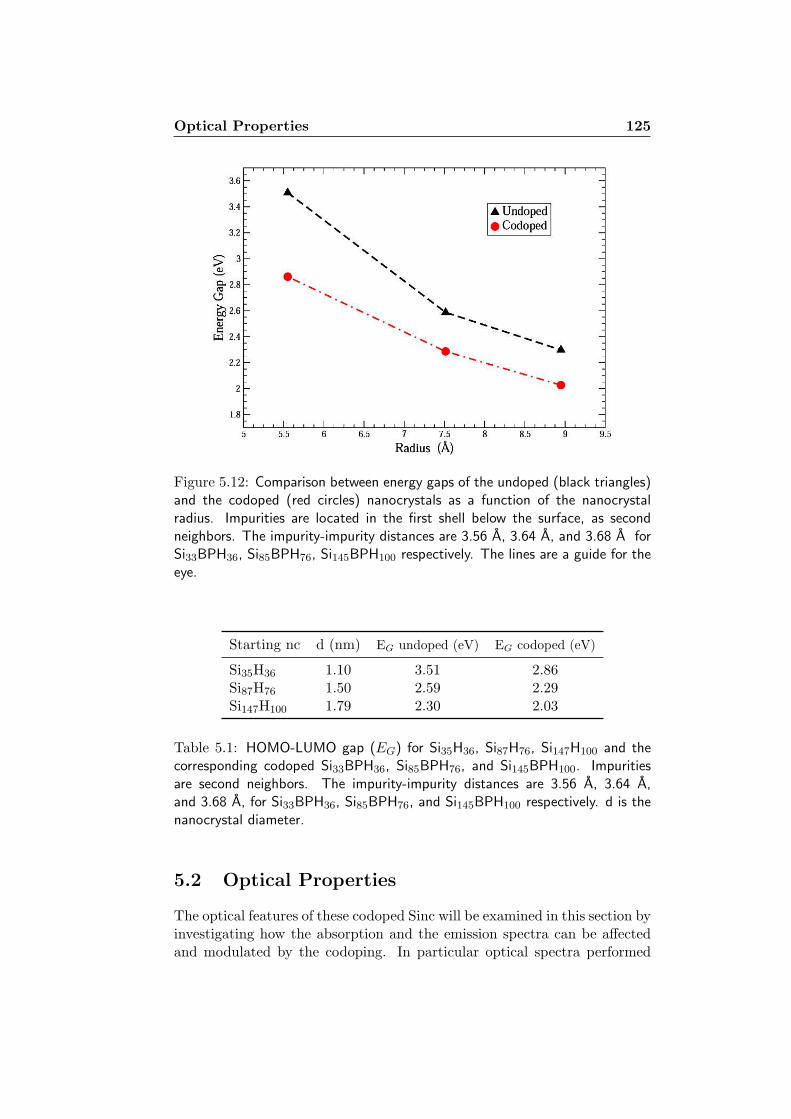
Optical Properties 125
Figure 5.12: Comparison between energy gaps of the undoped (black triangles)and the codoped (red circles) nanocrystals as a function of the nanocrystalradius. Impurities are located in the first shell below the surface, as secondneighbors. The impurity-impurity distances are 3.56 A, 3.64 A, and 3.68 A forSi33BPH36, Si85BPH76, Si145BPH100 respectively. The lines are a guide for theeye.
Starting nc d (nm) EG undoped (eV) EG codoped (eV)
Si35H36 1.10 3.51 2.86Si87H76 1.50 2.59 2.29Si147H100 1.79 2.30 2.03
Table 5.1: HOMO-LUMO gap (EG) for Si35H36, Si87H76, Si147H100 and thecorresponding codoped Si33BPH36, Si85BPH76, and Si145BPH100. Impuritiesare second neighbors. The impurity-impurity distances are 3.56 A, 3.64 A,and 3.68 A, for Si33BPH36, Si85BPH76, and Si145BPH100 respectively. d is thenanocrystal diameter.
5.2 Optical Properties
The optical features of these codoped Sinc will be examined in this section byinvestigating how the absorption and the emission spectra can be affectedand modulated by the codoping. In particular optical spectra performed

126 5. Back to the future: OptoElectronics
first in the Independent Particle Random Phase Approximation (IP-RPA)and next in the Many Body Perturbation Theory approach(GW-BSE) (seeSec.3) will be compared in order to bring out the effect of local field andmany body correction. In the RPA approach the absorption has been calcu-lated as the imaginary part of the dielectric function ǫ2(ω) expressed throughthe ”classical” Fermi golden rule [179]. To understand the role of dimen-sionality and impurity distance and to show the importance of includingmany-body effects in the optical spectra, we are going to present first theresult of a IP-RPA optical response for various codoped nanocrystals diffe-rent in dimensions and in impurity location (see Sec. 5.2.2), and next, wewill present a complete study of a codoped Sinc where we go beyond thesingle-particle approach within the GW-BSE framework (see Sec. 5.2.4).
5.2.1 Computational details
For all the calculations performed norm-conserving pseudopotentials havebeen used, without the inclusion of the non local commutator [VNL, r].Since it has been demonstrated that this term affects only the intensityof the absorption peaks in the spectrum without changing their positions,the commutator can be therefore neglected without loosing physical infor-mation. All the calculations performed are not spin-polarized. Howeverit should be noted that single-particle calculations for undoped Sincdone by Franceschetti and Pantelides [116] within the local spin-densityapproximation, show that the singlet-triplet splitting is significantly smallerthan the Stokes shift [170].
The nanocrystals optical response is evaluated for both the ground andthe excited state relaxed geometries computing the imaginary part of thedielectric function (ǫ2(ω)) through the well known Fermi golden rule, asexpressed in Eq.[ 3.11]. To the best of our knowledge, the present work isthe first up to now which takes care to study and understand the mecha-nisms that govern not only the absorption but in particular the emissionprocess from codoped Sinc. As remarked in the Introduction, the control ofemission of light from Silicon nanostructures is important to realize photonicdevices integrated with the traditional electronic dispositive. Therefore,the study of emission process leads to the knowledge of excited states bothfor extended or confined system; in particular the theoretical frameworkthat permits to treat and to manage with the excited states is still underdebate and upgrading. Approaches within the Many Body PerturbationTheory that permit to treat the many body effects by calculating the selfenergy correction via the GW approximation and to evaluate the role oflocal field and exciton effect through the solution of Bethe-Salpeter equa-tion, are still very computing demanding and supported by huge calculation.

Optical Properties 127
In this work we decide to go beyond the GS calculation and to simulatealso the excited state of our systems combining together two well knownapproaches in order to carry out a first estimation of the emission processwithout dealing for the moment with calculations based on Green Functions.The combination of a Constrain DFT (∆SCF) approach with the cal-culation of the imaginary part of the dielectric function ǫ2(ω) with alsothe inclusion of the many body effects, has led to an almost reliable andphysical treatment of the excited state [44, 47, 119, 117]. The emissionspectra have been calculated using the relaxed atomic positions of theexcited state combined with the electronic occupation of the groundstate. The excited state is characterized by an electronic configurationin which the highest occupied single-particle state (HOMO) containsa hole (h), while the lowest unoccupied single-particle state (LUMO)contains the corresponding electron (e), thus simulating the creation of aelectron-hole pair under excitation, as shown in Fig. 5.13(b), according
(a) Left panel: schematic representation of theground and excited state in the configurationspace. It’s possible to see the difference betweenthe absorption and the emission process, com-monly named Stokess shift.
(b) Neutral optical excitation (ab-sorption process) with the creationof an electron-hole pair which recom-bine radiatively (emission), and thecorresponding relaxed GS and EXCgeometries.
Figure 5.13: Schematic representation of the one-particle excitation process ina codoped Sinc.
to the Constrained-DFT approach (∆SCF) [114]. After excitation, dueto the change in the charge density and in presence of the electron-holepair, relaxation occurs until the atoms reach a new minimum energyconfiguration called relaxed geometry of the excited state. The new atomicpositions modify the electronic spectrum, implying that the levels involved

128 5. Back to the future: OptoElectronics
in the emission process change. This model assumes that the relaxationunder excitation is faster than the electron-hole recombination. Thedifference between the absorption and emission energies due to the differentatomic positions represents the nanocrystals Stokes shift [116, 57], that isschematically depicted in Fig. 5.13(a).
It’s worth pointing out that now the emission spectrum can be expressed asan absorption spectrum calculated in new structural geometry, that meansto calculate the emission exactly as the imaginary part of dielectric function(ǫ2(ω)), thus like an absorption, but with the electronic occupation of theground state and the relaxed structural geometry of the excited state. Itshould be noted that although ǫ2(ω) should only be used for calculatingthe nanocrystals absorption coefficient, it can also be used to get a firstapproximation for the emission spectra, simply because the emission canbe viewed as the time reversal of the absorption, whose main features arealso those of the emission spectra as one can see from the Fermi goldenrule [179]. To note that for the first time, the electron-hole interaction ishere considered in the emission geometry via a ∆SCF scheme, while sincenow excitation of nanoclusters has been studied calculating pair-excitationenergies [115, 119, 117]. It is worth mentioning that the photoluminescencespectra can be derived using the well known Van Roosbroeck and Shock-ley [180] relation which, again, involves the imaginary part of the dielectricfunction, ǫ2(ω). However, such a calculation requires the knowledge of theelectron and hole populations, at the working temperature, in the LUMOand HOMO states respectively. The populations, in turn, depends on theactual dynamics in the excitation and emission processes, including thenon radiative electron-hole recombination. In this work, nevertheless, wehave not considered any particular dynamics so that our emission spectracontains only the information related to both the transition energies andthe oscillator strengths.
In the second part of the section, we have gone beyond the single-particleapproach including in the calculation of the optical response of the systemthe many body effects, through the computation of the GW self energycorrection and the application of the Bethe-Salpeter equation in order totreat properly the two body electron-hole interaction (see Sec. 3). Since theinclusion of the self energy correction, the local field effects and excitonicinteraction makes the calculation very tough and very computationally de-manding, we take into account these many body effects (for the moment)only for the Si33BPH36 the smallest Sinc considered here.We have included the self-energy corrections by means of the GW approx-imation [181]. In a successive step, excitonic effects are include solving theBethe-Salpeter equation [131]. A further advantage of this procedure is thatthe inhomogeneity of the system is taken into account by properly includ-

Optical Properties 129
ing local fields effects [182, 183] This approach, in which many-body effectsare combined with a study of the structural distortion due to the impurityatoms in the excited state, allows a precise determination of the Stokes shiftbetween absorption and emission spectra [57].
5.2.2 Absorption and Emission: RPA results
The modifications induced in the electronic levels of the Sinc when addingdonor and acceptor impurities are reflected also in the optical features ofsingle and co- doped nanocrystals. What we expect is that with the arisingof new impurity states within the energy gap, new interesting transitionscould be originated.
”To dope or to codope?”
What is the best solution between the doping and codoping to obtain inter-esting and new optical features?With reference to the electronic structure of the doped and codoped Sincbased on the Si87H76-reference cluster, in Fig. 5.14 are reported the IP-RPA absorption spectra of the B and P singled doped cluster, Si86BH76 andSi86PH76 , compared with the corresponding spectra of the undopedSi87H76 reference nc. With respect to the undoped nc, the presence of asingle impurity within the nanocrystals determines new optical transitionsarising in the lower part of the energy spectrum, both in the case of B- orP- single doping as in Fig. 5.14. New strong peaks appear in the infra-redregion below the absorption onset of the undoped Sinc due to the interbandand also intraband transitions that involve the B and P impurity states andthe Si energy levels. These new optical features in the absorption spectrumcan be important for the possible applications in the field of infrared or alsoin Raman lasers technology [184]. Unfortunately this kind of single dopedSilicon Nanocrystals are very inefficient for the emission properties since,due to the breakdown of the k-conservation rule in Si nanocrystals makesAuger processes significantly more efficient than in the bulk: a kinematictemperature dependent threshold for the Auger process known for bulk isabsent in nanocrystals. Therefore, the branching ratio between rates of ra-diative and non-radiative Auger processes can significantly exceed the bulkvalue: the crystallites containing a shallow impurity are dark as reported byKovalev et al. [39].

130 5. Back to the future: OptoElectronics
Figure 5.14: Calculated imaginary part of the dielectric function (ǫ2(ω)) for thesingle doped Si86BH76 (blue line) and Si86PH76 (red line) compared with theundoped Si87H76 (black line) case. A Gaussian broadening of 0.1 eV has beenapplied.

Optical Properties 131
The simultaneously insertion of two impurities thus render the Sinccompensated: since no semi-occupied energy level now exist, the shallowimpurity energy levels arising within the gap will be then shown to beresponsible of new interesting optical features. In Fig. 5.15 we can see
Figure 5.15: Comparison between the undoped Si87H76 (solid line) and thecodoped Si85BPH76 (dashed line) single-particle absorption spectra. The im-purities are at a distance of 10.60 A. Arrows indicate the energy gaps. Thecalculated energy levels for the codoped nanocrystal are shown in the inset. AGaussian broadening of 0.1 eV has been applied. H stands for HOMO, L forLUMO.
the comparison between the IP-RPA absorption spectrum of the undopedSi87H76 and the codoped Si85BPH76 with impurities placed at a distanceof 10.60 A. With respect to the single doped cases before, one can seethat now several optical transitions arise below the absorption onset of theundoped nanocrystal. In particular due to the presence of both n- andp- type impurities, the overall valence electrons result to be compensated.The absorption onset of the codoped Sinc is shifted toward lower energies,with a consequent enhancement of the intensity of the transitions aroundthe 2.0 eV. These new transitions are due to the presence of new HOMOand LUMO states localized on the impurities, as described in Sec. 5.1 (seefor example Fig. 5.10). The inset of Fig. 5.15 clarifies how the peak locatedin the 2.0-2.2 eV energy region is related to contributions that involve the

132 5. Back to the future: OptoElectronics
HOMO-1, HOMO to LUMO, LUMO + 1 transitions; it should be notedthat for all these levels the wavefunctions are predominantly localized onthe impurities. If we compare these results with those of a single-dopedSinc [185], we note that the simultaneous presence of both impuritiesnaturally suppresses all the absorption energy structures present in theinfrared region (below 1 eV) of the single-doped spectra, thus giving newchance for an efficient emission of light in the visible range as confirmed bythe experimental outcomes by Minoru Fujii [37, 36, 33, 41].

Optical Properties 133
Figure 5.16: Single-particle absorption spectra of Si33BPH36 (black solid line),Si85BPH76 (red dashed line), and Si145BPH100 (dash-dotted blue line). In allcases the impurities are second neighbors. The impurity-impurity distances are3.56 A, 3.64 A, and 3.68 A for Si33BPH36, Si85BPH76, Si145BPH100 respec-tively. Arrows indicate the energy gaps. In the inset a zoomed view of thespectra onset. No Gaussian broadening has been applied.
Role of dimension and B-P distance
After this outcomes about the different effects between single doping andcodoping, our aim will be the investigation of the role played by the di-mensions and by the impurity distance on the optical features, in analogyto what has been done for the electronic properties. The role of the Sincdimensions on the absorption spectrum is shown in Fig. 5.16 where is re-ported the absorption onset for the three different nanocrystals size withimpurities located at the same distance. The Si33BPH36 , Si85BPH76 andSi145BPH100 , with diameters of 1.10 nm, 1.50 nm and 1.79 nm respectively,present substitutional impurities located as second neighbors with corre-sponding distances of 3.56 A, 3.64 A and 3.68 A. Looking at the figure twomain aspects emerge:
• on increasing the nanocrystals size the absorption gap is strongly re-duced (see arrows in Fig. 5.16). This trend well agrees with the quan-

134 5. Back to the future: OptoElectronics
tum confinement effect of the Sinc already highlighted in several workon hydrogenated Sinc (see for example [44]): the energy gap and theabsorption one decrease as the dimension of the Sinc increase, sincethey coincide for the biggest nc, toward the bulk limit. This is trendalso confirms the experimental results of Fujii, according to them, theaverage dimension of codoped Sinc that contributes to emit light inthe visible range is around 5 nm;
• an increase of the Sinc diameter (i.e. a decrease of the impurity weightwith respect to the total number of atoms, thus we can say a loweringof ”concentration”) results in a lowering of the intensity for the transi-tions that involve the impurities. This can probably be related to thequenching of the effect that spatial confinement on the localization inreal space of the impurity wavefunction involved in the transition; insmaller Sinc due to the better overlap between the electron and holeenvelop function, it should be expected infact strong enhancement ofe-h interaction.
Going on, another interesting investigation has been the comprehensionof the role played by the impurity-impurity distance on the absorption spec-trum, done following the same approach used adopted for the electronicproperties. The absorption spectrum of the Si145BPH100 has been calculatedby varying the distance between impurities, placing the P atom on sites II,III, IX, and X respectively (see for comparison Fig. 4.6). The IP-RPA ab-sorption spectrum at issue are reported in Fig. 5.17 where in particular theattention is focused on the onset in order to the shape of the peaks changenear the absorption edge. Here a shift of the absorption gap to lower energyon increasing the distance between the impurities is observed (see arrowsin Fig. 5.17). Moreover, also the intensity is affected by the impurity dis-tance. The intensity gets lower when the impurities are at a larger distances,whereas stronger transitions arise when the impurities are closer due to theincreased overlap between HOMO and LUMO states which are mainly lo-calized on the impurity site (as demonstrated previously). Nonetheless theoptical transitions near the band edge (indicated by arrows in Fig. 5.17) ex-hibit weaker oscillator strengths, as sign that to these transitions contributealso states around the energy gap, such as HOMO-1 and LUMO+1.

Optical Properties 135
Figure 5.17: Single-particle absorption spectra of Si145BPH100 Sinc with impu-rities placed at different distances (see the inset). Arrows indicate the energygaps. Roman numbers refer to the sites occupied by the P atom with respectto the B one (see Fig. 4.6). No Gaussian broadening has been applied.
5.2.3 Absorption, Emission and Stokes Shift: IP-RPA re-
sults
Here are presented and discussed the results for both absorption and emis-sion spectra and the consequent Stokes Shift calculated for two codopedSinc. The Stokes shift, as already defined, represents the difference betweenthe absorption and the emission gap. As already depicted in Fig. 5.13(a), wereport here in Fig. 5.18 a more detailed scheme of a Stokes shift relaxation.
The quantity ǫAex and ǫBex represent respectively the Absorption and the Emis-sion gap as defined via a Constrain DFT-∆SCF approach used in precedingwork [44, 119, 117, 116, 186] to estimate with success these quantities with-out using the Green Function approach. In these papers it has been demon-strated that treating the HOMO-LUMO gap for the ground and the excitedstate as the proper absorption and the emission energies respectively leadsto wrong results, in particular for smaller nanocrystals, since in particularthe GS HOMO-LUMO gap tends to be always smaller than the absorptionenergy while the EXC HOMO-LUMO gap tends to assumes larger valuesthan the emission energy.

136 5. Back to the future: OptoElectronics
Figure 5.18: Schematic representation of a Stokes shift relaxation. In position(1), the cluster is in its electronic ground state, and the atomic geometry isrelaxed to its lowest energy configuration. On absorption of a photon, thenanocluster undergoes a vertical electronic excitation from (1) to (2). Oncein the excited electronic state, the atomic geometry of the cluster relaxes to alower energy configuration [from (2) to (3)]. Finally, the excited electron andhole recombine via another vertical transition, (3) to (4). The Stokes shift isdefined as ǫAex − ǫBex .
Nevertheless in this work we will refer to the HOMO-LUMO gap of theGround and Excited State as the ”absorption and emission gap”. Since thecomputation of the absorption and emission energies ǫAex and ǫBex are verytime consuming and computationally demanding. We decided for sake ofsimplicity to used the HOMO-LUMO gaps amounts to indicate absorptionand emission energies, being aware of the discrepancies but considering also,as shown in [44], that the error made tends to reduce as the dimensionsof the Sinc increase, thus leading our values close to the ”correct ∆SCF”absorption and emission energies.
The calculations have been performed for two Sinc of different sizes,taking, in the larger Sinc, the impurities located at different distances.In the Si33BPH36-nc, the impurities are placed like second neighbors, asthe possible largest distance within the Sinc (DBP =3.56 A), while in theSi85BPH76 the impurities are at the minima (DBP =2.00 A) and largest dis-

Optical Properties 137
Si33BPH36 Si85BPH76
d (nm) 1.10 1.50
DBP (A) 3.56 2.00 10.60Abs. (eV) 2.77 2.32 1.75Ems. (eV) 1.78 2.20 1.36∆ (eV) 0.99 0.12 0.39
Table 5.2: Absorption and emission energy gaps (and their difference, 5th row)calculated as HOMO-LUMO differences in the ground and the excited relaxedgeometries configuration, respectively. The results are obtained within the DFTsingle-particle approach. d is the nanocrystal diameter, DBP is the distancebetween impurities and ∆ the calculated Stokes shift between absorption andemission energy gaps.
tance (DBP =10.6 A) within the Sinc, in order to point out the effect onthe emission spectra in particular. As shown in Table 5.2, both the absorp-tion and emission HOMO-LUMO energies are affected by nc dimensionsand impurity-impurity distance. With regard to the first parameter, wenote that the Stokes shift strongly depends on the size showing a strongdecrease on increasing the diameter of the Sinc. This is due to the fact thatfor larger nanocrystals the excitation determines a minor distortion of thegeometry. Concerning the second parameter, we see that the Stokes shifttends to slightly increase with B-P distance although this effect is small ifcompared with the lowering due to the increase of the Sinc dimensions. Thecomparison between these results and the ones previously obtained for un-doped clusters (0.92 eV for the Si35H36-nc [44] and 0.22 eV for the Si87H76-nc[117]) confirm that the Stokes shifts is mainly determined by the nanocry-stals size, but that nevertheless it depend slightly on the presence of theimpurities and also on their mutual distance. This trend is corroborated byFig. 5.19 in which the absorption and emission onset for the Si85BPH76 ncare shown for the two different kind of impurity configuration.

138 5. Back to the future: OptoElectronics
The HOMO-LUMO transition (absorption gap) in Si85BPH76 (1.75 eV,bottom panel) is almost dark when the two impurities are far apart andbecomes instead allowed (2.32 eV, top panel) when their distance decreases.As discussed before, this oscillator strength enhancement in the absorptionspectrum is a consequence of the character of the HOMO and LUMO statesin the two cases, both highly localized on impurity sites, but subjected to adifferent overlap.
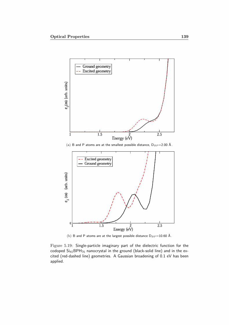
Optical Properties 139
(a) B and P atoms are at the smallest possible distance, DBP =2.00 A .
(b) B and P atoms are at the largest possible distance DBP =10.60 A .
Figure 5.19: Single-particle imaginary part of the dielectric function for thecodoped Si85BPH76 nanocrystal in the ground (black-solid line) and in the ex-cited (red-dashed line) geometries. A Gaussian broadening of 0.1 eV has beenapplied.

140 5. Back to the future: OptoElectronics
The emission (red-dashed lines in Fig. 5.19) spectra is red shifted withrespect to the absorption (black-solid lines in Fig. 5.19) toward lower energyvalues. This red shift is a consequence of the geometry relaxation in the ex-cited state due to the excess energy necessary for promoting of an electronin the LUMO level. The amount of Stokes shift is strongly influenced bythe size and the B-P distance. Increasing the dimension of the Sinc, theStokes shift decreases according to the same trend figured out for the un-doped hydrogenated Sinc[44]. At the same time, looking at Fig. 5.19, theStokes shift strongly decrease when impurity are brought closer (DBP =2.0A), since in this case the emission gap become more similar to the absorp-tion energy. Nonetheless in both cases the presence of two Boron and Phos-phorous impurities determines in emission an intensity enhancement of theHOMO-LUMO transition, whose peak position moves in energy spectrumaccording to the distance at which the impurities are placed: increasing theB-P distance leads to a more strong shift of the emission peak toward lowerenergies. This result fits very well the experimental results of the work ofMinoru Fujii, which shows that introducing shallow n− and p− type impu-rities within the Sinc, it’s possible to tune the photoluminescence (PL) ofthe nc, in particular below the Silicon bulk-band-gap PL value [38].It’s worth pointing out that only with a ”simple” single-particle RPA ap-proach the results presented here are in really fair agreement with the exper-imental outcomes of Minoru Fujii [38, 37, 36]. The shift of the emission peaktoward lower energies well represents the analogous shift of the PL peak be-low the bulk band gap limit obtained by the experimental setup of Fujii andcoworkers. In particular we recover the real possibility to control and tunethe emission by playing with dimensions of Sinc, and most important withthe distance and the position of impurities inside the nanoclusters.

Optical Properties 141
5.2.4 Absorption, Emission and Stokes shift: Many-Body
results
In order to give a complete description, within the many-body framework, ofthe codoped Sinc response to an optical excitation, we consider both the self-energy corrections by means of the GW method to obtain the quasiparticleenergies and the excitonic effects through the solution of the Bethe-Salpeterequation. The effect of local fields is also included, to take into account theinhomogeneity of the systems.
The heavy GW-BSE calculation is made considering a 50 a.u. latticeparameter large FCC supercell in order to reduce the number of planewaves. For the GW calculation have used the non self-consistent G0W0 ap-proach within the RPA plasmon pole approximation. through a planewave-frequency space code. The correlation part of the self-energy Σc has beencalculated using 10081 plane waves, while 49805 plane waves have beenused for the exchange part Σx. Then, the full excitonic Hamiltonian hasbeen diagonalized considering more than 8000 transitions using the EXCcode [158]. The complete matrix calculation WG,G′(q; ω) have been diago-nalized by using 4573 G vectors while the calculation without coupling hasbeen performed using a 6975 plane wave basis set.
Since the GW-BSE calculation [158] are very computing demanding, wehave only considered the smaller codoped nanocrystal Si33BPH36 (see Fig.4.3(a)). In this particular cluster, we found that Local fields effects are, al-though not negligible, of minor importance with respect to GW and excitoniceffects. It is anyway essential to include all of them (LF and many-body)in order to get the final converged spectrum shown in Fig. 5.20. In order tocarry out emission spectra calculations, we use the excited state geometryand the ground state electronic configuration. As already noted before, inthis case ǫ2(ω) corresponds to an absorption spectrum in a new structuralgeometry. In other words, we consider the emission as the time reversal ofthe absorption.[?, 57] Thus, the electron-hole interaction is here consideredalso in the emission geometry.
Fig. 5.20 shows the calculated absorption and emission spectra fully in-cluding the many-body effects. The electron-hole interaction yields signifi-cant variations with respect to the single-particle spectra (see for a compar-ison Fig. 5.19), with an important transfer of the oscillator strength to thelow energy side. Moreover, in the emission spectrum the rich structure ofstates characterized, in the low energy side, by the presence of excitons withlargely different oscillator strengths, determines excitonic gaps well belowthe optical absorption onset. Thus the calculated emission spectrum results

142 5. Back to the future: OptoElectronics
Figure 5.20: Absorption (black-dashed line) and emission (red -solid line)many-body spectra of Si33BPH36.
to be red shifted to lower energy with respect to the absorption one. Thisenergy difference between emission and absorption, the Stokes shift, can belead back to the relaxation of the Sinc after the excitation process.
The new important features that appear in the emission many-body spec-tra are related to the presence of both B and P impurities as showed byFig. 5.21, which gives the real-space probability distribution |ψexc(re, rh)|2for the bound exciton as a function of the electron position re when the holeis fixed in a given rh position. In this case the hole is fixed on the Boronatom (labelled by the white X) and we see that the bound exciton is mainlylocalized around the Phosphorus atom.

Optical Properties 143
Figure 5.21: Excitonic wave function of Si33BPH36 (atom colors as inFig. 4.3(a)). The grey isosurface represents the probability distribution|ψexc(re, rh)|2 of the electron with the hole fixed on the B impurity.
This confirms the consideration pointed out in the experiments: the com-pensated doping helps to localize the carriers further and to increase theprobability of a quasi-direct electron-hole radiative recombination with in-tense emission of light, such as represented by the strong excitonic peakin emission spectrum of Fig. 5.20. From Table 5.3, it can be seen that thesingle-particle DFT results strongly underestimate the absorption and emis-sion edge with respect to the GW+BSE calculation, in which the excitoniceffect are taken exactly into account. This means that, in this case, thecancellation between GW gap opening (which gives the electronic gap) andBSE gap shrinking (which originates the excitonic gap) is only partial [187].
The difference between the GW electronic gap and the GW+BSE opticalexcitonic gap gives the exciton binding energy Eb. We note the presenceof exciton binding energies as big as 2.2 eV, which are very large if com-pared with bulk Si (∼ 15 meV) or with carbon nanotubes[188, 189] whereEb ∼ 1 eV, but similar to those calculated for undoped Sinc [57] of similarsize and for Si and Ge small nanowires [190, 191].
The differences between full many-body calculations and single-particleresults are of 0.55 eV and 0.41 eV for absorption and emission energy gapsrespectively, and of 0.14 eV between the two Stokes shifts. It is interesting tonote that the HOMO-LUMO transition in the emission spectrum at 2.20 eV

144 5. Back to the future: OptoElectronics
Si33BPH36 DFT GW GW+BSE
Abs. (eV) 2.80 5.52 3.35Ems. (eV) 1.79 4.37 2.20∆ (eV) 1.01 1.15 1.15
Table 5.3: Absorption and Emission energies calculated as HOMO-LUMOenergy difference within the single-particle DFT, the many-body GW and theGW+BSE approaches. ∆ is the calculated Stokes shift between absorptionand emission energy gap. The 2.20 eV energy corresponds to an almost darktransition.
is almost dark while an important excitonic peak is evident at about 2.75 eV(see Fig. 5.20), again red-shifted with respect to the first absorption peak.As expected, what comes out is the importance of fully taking into accountthe many-body aspect of the problem in order to overcome the limits of thesingle-particle approach.
To resume, the main effort of the work presented since now is to shed morelight on the possibility to tune the electronic properties of the Sinc playingwith the codoped impurities to achieve a well defined technique that per-mits to engineer at the end the absorption and the emission of radiationof these nanocrystals. The doping technique, commonly used to modifythe electronic properties to achieve better conductivity and high performingtransport features, has been here converted into a method to improved andspeed up the possibility to engineer the optical features instead, in partic-ular to tune the emission of light from Silicon-based nanostructures whichcan be used for technological innovative application, in optoelectronic andtelecommunications.
6Multidoping... is better
Vagar mi fai co’ miei pensieri su l’ormeChe vanno al nulla eterno; e intanto fugge,questo reo tempo, e van con lui le tormedelle cure onde meco egli si strugge;e mentre io guardo la tua pace, dormequello spirto guerrier ch’entro mi rugge.
Alla Sera, Ugo Foscolo
In this section we’ll investigate how the formation energy, the electronicand optical features of the Silicon nanocrystals can be influenced by theinsertion of more impurities, in the specific by adding one, two or threemore impurities with respect the initial codoped nanocrystal.
6.1 The systems
We called this insertion of several impurities multidoping. This proce-dure tends to simulate a heavy doping with compensated B and P impu-rities and it’s similar to what is done in the bulk Silicon wafers in tradi-tional microelectronics to improve or tune transport and optical properties[192, 193, 194, 195]. Now the multidoping has been realized on Silicon nano-crystals in order to investigate the role played by heavy doping with B andP and also the effect of a variation of impurity concentration on the stabilityand on the electronic and optical feature of the Sic. The starting codopednc configuration is the most stable one found in the previous section, wherethe B and P impurities are placed like second neighbors at a distance ofDBP =3.68 A, in site II with reference to Fig. 4.6. Then more dopant atomshave been added to the yet codoped Sinc in order to achieve a Sinc with
145

146 6. Multidoping... is better
Figure 6.1: Some compensated multidoped nc with an even number of impu-rities: Si143H100:BBPP-nc (left side) and Si143H100:BBBPPP-nc (right side).Yellow balls represent Si atoms, while the white balls are the H atoms usedto saturate the dangling bonds. P atoms are dark brown and B atoms aremagenta.
three impurities as in Fig. 6.2 or four or six impurities such as depicted inFig. 6.1.
Then one single impurity has been added in order to produce an excessof dopants for each species: an excess of Boron with two B atoms andone P atom in the Si144BBPH100 or an excess of Phosphorus with twoP atoms an one B atom in the Si144BPPH100. In the end we obtain theSi143BBPPH100 and the Si1413B3PH100 by adding respectively two B andtwo P atoms, in the former case and three B and three P dopants in thelater one. These Sinc containing two and three pairs of n− and p− typeimpurities are compensated as the Si145BPH100. For what concern this lastSinc, one configuration with the two B-P pairs are placed within the nc ata distance of Dpairs=12.11 A, and the other one in which the two pairs arefound at a distance of Dpairs=13.59 Ain order to understand which effectthe mutual position can bring about.

Structural properties and Formation Energy 147
Figure 6.2: The uncompensated multidoped nc with an odd number of im-purities: Si144H100:BPP-nc (left side) and Si144H100:BBP-nc (right side).Yellow balls represent Si atoms, while the white balls are the H atoms usedto saturate the dangling bonds. P atoms are dark brown and B atoms aremagenta.
6.2 Structural properties and Formation Energy
The insertion of one or more impurities in the already codoped Sinc deter-mines no relevant modification in the geometry of the nanocrystal. Addingone or two more impurities within the codoped Sinc, it results in a generallowering of the Formation Energy, both for nanocrystal with an even andodd number of dopants atoms as shown in Fig. 6.3 where the FE of the singledoped, codoped and multidoped Si147H100-based nanocrystal are reportedfor comparison. It can be seen that the nanocrystal with an odd numberof impurities (one or three) have always the highest positive FE values withrespect to the Sinc with an even number of dopants shared in equal partof n− and p− type impurities. In particular the uncompensated Sinc withimpurities, Si144BBPH100 and the Si144BPPH100, presents FE values lowerwith respect the uncompensated single doped nc. Thus, although the dopingwith one or three impurities results to be less favorite and preferred withrespect the doping with an even number of compensated impurities, it seemsmore easier to produce an excess of Boron or Phosphorous in an already

148 6. Multidoping... is better
Figure 6.3: Formation Energies for single, co- doped and multidoped Si na-nocrystals. In red are reported the FE for compensated Sinc (with an evennumber of impurities), in black are shown the FE for Sinc with an odd numberof impurities.
doped Sinc, than in a undoped hydrogenated Silicon nanocrystal.
As shown from Table 6.1 it is evident that the Sinc with an even numberof impurities infact assume lower values then the others. The FE becomesmore negative as the number of n− and p− type dopant pairs increase:the Si1413B3PH100 infact presents the smallest negative Formation Energyvalue among all the cases take into account. This suggests that by aug-menting the impurity concentration, or better, increasing the number ofcompensated donor-acceptor B-P pairs in the nanocrystal, it should moreeasier to multidope the nanocrystals. Moreover also the distance betweenthe B-P impurity pairs influence the Sinc stability: increasing the distancebetween the B-P pairs the FE values decrease, assuming more negative val-ues. As confirmed by the numerical values in Table 6.1, as in the case ofsimple codoping, multidoping is much easier to realize when the impurityare in even number inside the nanocrystal, in order to have same number ofdonor and acceptor dopant atoms; furthermore, increasing the stability ofthe doped nc by adding more impurities, cancel out also the possible depen-

Structural properties and Formation Energy 149
Cluster Formation Energy Energy Gap(eV) (eV)
Si146BH100 1.11 2.08Si146PH100 0.74 0.13Si145BPH100 -0.32 2.03Si145BPH100 0.15 1.59Si144BBPH100 0.84 2.02Si144BPPH100 0.58 0.15Si143BBPPH100
DBPpairs=12.11 A -0.42 1.97DBPpairs=13.59 A -065 2.01
Si1413B3PH100 -0.97 1.92
Table 6.1: Formation Energy and Energy Gap (see text) for the Single Doped,Codoped and the Multidoped Silicon nanocrystals.
dence of the Formation Energy on the impurity position within the Siliconlayers of the nc. By mapping through an atom-probe tomography the con-centration of heavily doped Boron atoms within Si nanostructures volumes[196], it results that B atoms in great excess tend to segregate to the grainboundaries, also producing small impurity clusters; this confirms our findingon the decreasing of FE when more impurities are close each other, in par-ticular the values found for the Si1413B3PH100-nc. The gain in stability ofthe Sinc with the increase of the number of impurities inserted, reflects alsoa permanent difficulty in the control and estimation of the real number ofimpurities inside the nc during all the experimental steps of doping process.

150 6. Multidoping... is better
6.3 Electronic structure
Here we investigate how the electronic levels are influenced by adding oneor two more impurities to the yet codoped Si145BPH100-nc. Looking atthe electronic structure in Fig. 6.4, the two Si-nc with three impurities,present a similar behavior to those corresponding to B or P single-dopedSi-nc, depicted in the previous section of the thesis. Every new dopantinserted gives raise to a new impurity level, which is half occupied. Fromtheoretical and experimental works in literature, it is well known that largeconcentrations of donors and acceptors in a semiconductor cause a reductionof the forbidden gap [?] and the so-called ”band tailing” effect due to therandom impurity distribution of donors and acceptors that forms a broadband near the energy gap edge [195, 194].
Figure 6.4: Comparison between the electronic levels the Γ point for thecodoped Sinc and the uncompensated multidoped nc with an odd number ofimpurities. Left: Si145BPH100-nc (DBP =13.28 A). Middle: Si144BBPH100-nc.Right: Si144BPPH100-nc. Alignment has been performed locating at the sameenergy the fully occupied levels with the same type of localization.
Thus looking at Table 7.3 we see that the HOMO-LUMO energy differ-ence for the nanoclusters with an odd number of impurity atoms are verysimilar: 2.02 eV for the Si144BBPH100-nc with respect to 2.08 eV for the Bsingle doped case (Si146BH100), and 0.15 eV for the Si144BPPH100-nc withrespect to 0.13 eV for the P single doped case (Si146PH100) respectively.Besides, another time, when the impurities are compensated, as in thecase of Si143BBPPH100-nc, the system becomes semiconductor: now the

Electronic structure 151
Figure 6.5: Comparison between the electronic levels the Γ point forthe compensated multidoped nc with an even number of impurities.Left: Si143BBPPH100-nc (Dpairs=12.11 A). Middle: Si143BBPPH100-nc(Dpairs=13.59 A). Right: Si141BBBPPPH100-nc. Alignment has been per-formed locating at the same energy the fully occupied levels with the sametype of localization.
HOMO contains again two electrons, and the value of the energy gap (1.97eV) is between the two EG values associate to the two opposite codopedconfiguration for the Si145BPH100 with impurities located at differentdistance (2.03 eV for impurities closer each other and 1.59 eV for impuritiesat the opposite side of the Si-nc). Furthermore regarding Fig. 6.5, whereare compared the multidoped Sinc with an even number of impurities, withtwo or three B-P impurity pairs, one can see that the energy gap remainspractically constant with respect to the distance between the B-P impuritypairs (in the Si143BBPPH100) and also with respect to the increasing of thenumber of compensated B-P impurity pairs.
In from Fig. 6.6 are reported the HOMO and LUMO states square modulusfor the compensated multidoped Sinc. Once again it is confirmed the trendalready depicted in the case of codoped compensated Sinc: the HOMO stateis mainly localized on the Boron impurity site, while the LUMO states isprincipally centered around the Phosphorus atom. Nonetheless there are

152 6. Multidoping... is better
some differences due to the excess of impurities. It comes out that whenimpurities of the same valence kind are coupled along the nanocrystal di-ameter the impurity wavefunctions tend to be localized on the two impuritysites. This is what happen in the Si143BBPPH100-nc (DBPpairs=13.59) (mid-dle panel) where due to this sort of particular ”coupling” of the B and Patoms of the two pairs, the HOMO states is spread along the B-B direction,while the LUMO state is delocalized along the direction linking the twoP atoms. On the opposite case, where two dopants with different valancecharge are on the same linking diameter, the two wavefunction interferesdestructively leaving the HOMO and LUMO mainly focused respectively onthe B and P atom of the two pairs, as shown in the first panel of Fig. 6.6.This particular behaviour is confirmed by the localization of orbitals in theSi1413B3PH100-nc where due to the constructive overlapping among the im-purity states related to the P atoms, the LUMO state is spread all over thethree impurity sites within the nc.

Optical Absorption 153
6.4 Optical Absorption
The calculated optical absorption spectrum of Si143BBPPH100nc hasbeen compared in Fig. 6.7 with the corresponding spectra of theSi145BPH100 codoped with impurities placed at two different distanceswithin the nanocrystal, at site II and site IX with reference to the”Si145BPH100 impurity path” of Fig. 4.6. For what concern the two codopedSi-nc we observe a shift of the absorption onset toward lower energy on in-creasing the distance between impurities. It is worth pointing out that whenimpurities are at larger distance the transition intensities near the bandedges become weaker due to a small oscillator strengths. When, instead,impurities are closer each other due to the strong localization of HOMO andLUMO on the impurity sites, the transitions near the band edge are moreintense and involve in particular the Homo-1, Homo, Lumo and Lumo+1levels. The multidoped Si143BBPPH100-nc shows an onset which is inter-mediate in energy between the two codoped cases, now the stronger opticaltransitions are far from the HOMO-LUMO gap and peaked in the 2.0-2.2eV energy region, thus involving transitions between levels within the va-lence and the conduction band. The particular localization of HOMO andLUMO states depicted in the section before can offer a possible explanation.Due to the low overlap between the HOMO and LUMO state due to the in-terference among the impurity states, the optical transitions result almostdark and unfavored. We can think that when the dopant atoms with samecharge valence couple an enhancement of the collective impurity state arise,leading as in the two cases of Fig. 6.6 to a better overlap of HOMO andLUMO states and thus to an increase of oscillator strength of transitionsthat involves levels around the band edge.
Moreover, as explained in [195], in heavily compensated doped Silicon therelative decrease in intensity of direct transitions can be due to the screen-ing of the electron-dopants interaction by the compensating impurities andcharge carriers; this screening can partially block the momentum transfer tothe impurities thus leading to a quenching of the intensity of the direct no-phonon mediated optical transition involving the impurity levels, as infactappear also in the spectrum in Fig. 6.7.

154 6. Multidoping... is better
Figure 6.6: HOMO and LUMO square modulus contour plots calculatedfor the compensated multidoped Sinc. Upper panel: Si143BBPPH100-nc(DBPpairs=12.11). Middle panel: Si143BBPPH100-nc (DBPpairs=13.59).Lower panel: Si1413B3PH100-nc. The isosurfaces correspond to 20% of themaximum value.

Optical Absorption 155
Figure 6.7: The imaginary part of the dielectric function ǫ2(ω) for theSi145BPH100 Si-nc with impurities placed at different distances and for the mul-tidoped Si143BBPPH100-nc (see the inset). Arrows indicate the HOMO-LUMOenergy gaps. The roman number refer to the site occupied by the P atomwith respect to the B one (see Fig. 4.6). The arrows indicate the absorptionthresholds.


7Codoped Silicon Nanowires
Ramble on,And now’s the time,the time is nowTo sing my song.
Ramble on, Led Zeppelin
The Silicon Nanowires (Sinw) are semiconducting one-dimensional (1D)nanostructures which are attracting in the last years increasing interest forpotential nanoelectronic and nanophotonic applications. Among all the one-dimensional nanostructures, such as the carbon nanotubes or nanowires, theSilicon nanowires offer the biggest advantage to be compatible with the ex-isting silicon-based microelectronics. Moreover the possibility to tailor theirelectronic properties by changing thickness, orientation, surface morphol-ogy and doping is another important point in their favor [34, 35]. Severalab-initio studies on Si-nw are present in the literature. They are mainlyconcentrated on H-passivated or pristine Si-nw and demonstrate the depen-dence of the energy band gap from the wire diameter and from the surfacemorphology [12, 197, 198, 199, 200, 191]. Instead, few investigations havebeen dedicated to the influence of the electronic and transport propertiesfrom doping [201, 43]. In particular, due to the application in electronicdevices, the main efforts have been devoted to the study of B and P singledoped Si-nw, while only one ab-initio study has investigated the BP codop-ing [43]. For this reason, in complete analogy with the Si-nc, here is resumedthe systematic analysis performed on the effect of the Boron and Phospho-rous codoping on Sinw, concentrating not only on the structural propertiesbut also on how doping influences the electronic and optical properties.
157

158 7. Codoped Silicon Nanowires
7.1 The systems
The Silicon Nanowires considered here are isolated wires passivated at sur-face with hydrogen in analogy with the nanocrystals and oriented along the[110] direction. Their geometrical structure is the same used by M. Brunoand coworkers [191, 190] in their study of the electronic and optical prop-erties of undoped Silicon and Germanium nanowires. The same nanowiresstructures have been previously described in the work by Filonov et al. [202].It comes out that there are two main parameters defining the structure of ananowire:
• linear cross section l : the maximum linear distance between twobulk atoms belonging to the same plane; as depicted in Fig. 7.1 is thenpossible to characterize wires grown along different directions with thesame parameter l.
Figure 7.1: Unit cell projections onto the basis plane of the [110] orientednanowire. Yellow ball are Silicon atoms, the white one the hydrogens. Si atomslabelled with the red X belong to the same atomic plane. As described in [202],the value of the linear cross section reported is l=0.8 nm.
• effective diameter d :
d = 2
√A
π
where A is the cross section of the wire. One point of investigationinfact will deal with the scaling of the electronic and optical featureswith respect the effective diameter of the nanowire and with the com-parison with experimental evidence.

The systems 159
Here Silicon nanowires with two different values of linear cross section takeinto account: one with l=0.8 nm, as depicted in Fig. 7.2, and the other alittle bit bigger with l=1.2 nm, as in Fig. 7.4, in order to investigate also thedependence on the dimensions and therefore on the increasing of the numberof atoms. All the Sinw are passivated at the surface with hydrogen as donepreviously with the silicon nanocrystals and as free standing nanowires, arestuck within large supercell with a sufficiently portion of vacuum interposedbetween the period replicas.
• Silicon Nanowire (l=0.8 nm) - Si16H12 The Si16H12 nanowire isconstituted by 16 Si atoms and 12 H atoms in the unit cell and a linearcross section of l=0.8 nm . The direction of growth is along the [110]as one can see in Fig. 7.3
• Silicon Nanowire (l=1.2 nm) - Si30H16 The Si30H16 nanowire hasa larger cross section with 30 Si atoms and 16 H atoms in unit cell, asin Fig. 7.4. The [110] growth direction is shown in Fig. 7.5.
For what concern the computational details, the DFT-total energy cal-culations have been performed through the Quantum Espresso package [?],while the many-body calculations have been carried out using this time theoptic code SELF [157] developed in Rome in Tor Vergata. In table 7.1are shown the details of the total energy calculations for the two kind ofnanowires.
Si16H12 Si30H16
diameter 8 A 12 Aunit cell (Bohr) 7.19× 40.68× 40.68 7.19× 50× 50Energy cutoff 30 Ry 30 Ryk-point mesh 16× 1× 1 8× 2× 2shift k 0.5 1 1 0.5 1 1
Table 7.1: Technical details of the ground state calculations performed onthe nanowires.
In this work we moved from the previous outcomes by Bruno, Palummo,Ossicini et al. [191, 190] related to the study of electronic and optical fea-tures of undoped Silicon and Germanium nanowires, and we add one or twosimultaneously impurities of Boron and/or Phosphorous in substitutionalsites within the nanowires.
To the best of our knowledge the majority of works combining impuritiesand Silicon nanowires have been related since now to modify the conductivityfeatures for transport applications, like recent studies conduct by Fernandez-Serra and Xavier Blase [201, 42], Riccardo Rurali [199] and coworkers and
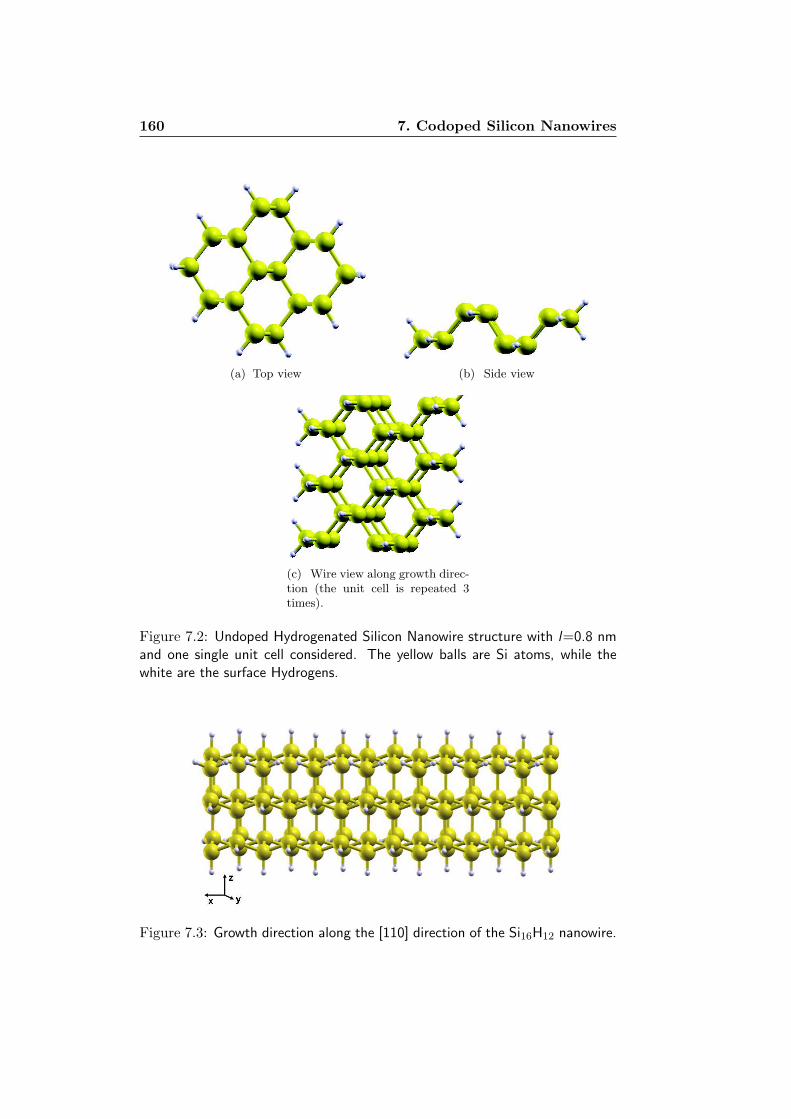
160 7. Codoped Silicon Nanowires
(a) Top view (b) Side view
(c) Wire view along growth direc-tion (the unit cell is repeated 3times).
Figure 7.2: Undoped Hydrogenated Silicon Nanowire structure with l=0.8 nmand one single unit cell considered. The yellow balls are Si atoms, while thewhite are the surface Hydrogens.
Figure 7.3: Growth direction along the [110] direction of the Si16H12 nanowire.
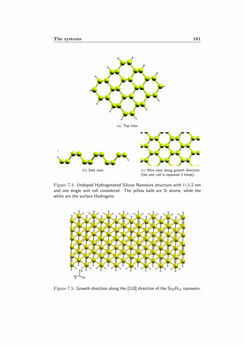
The systems 161
(a) Top view
(b) Side view (c) Wire view along growth direction(the unit cell is repeated 3 times).
Figure 7.4: Undoped Hydrogenated Silicon Nanowire structure with l=1.2 nmand one single unit cell considered. The yellow balls are Si atoms, while thewhite are the surface Hydrogens.
Figure 7.5: Growth direction along the [110] direction of the Si30H16 nanowire.
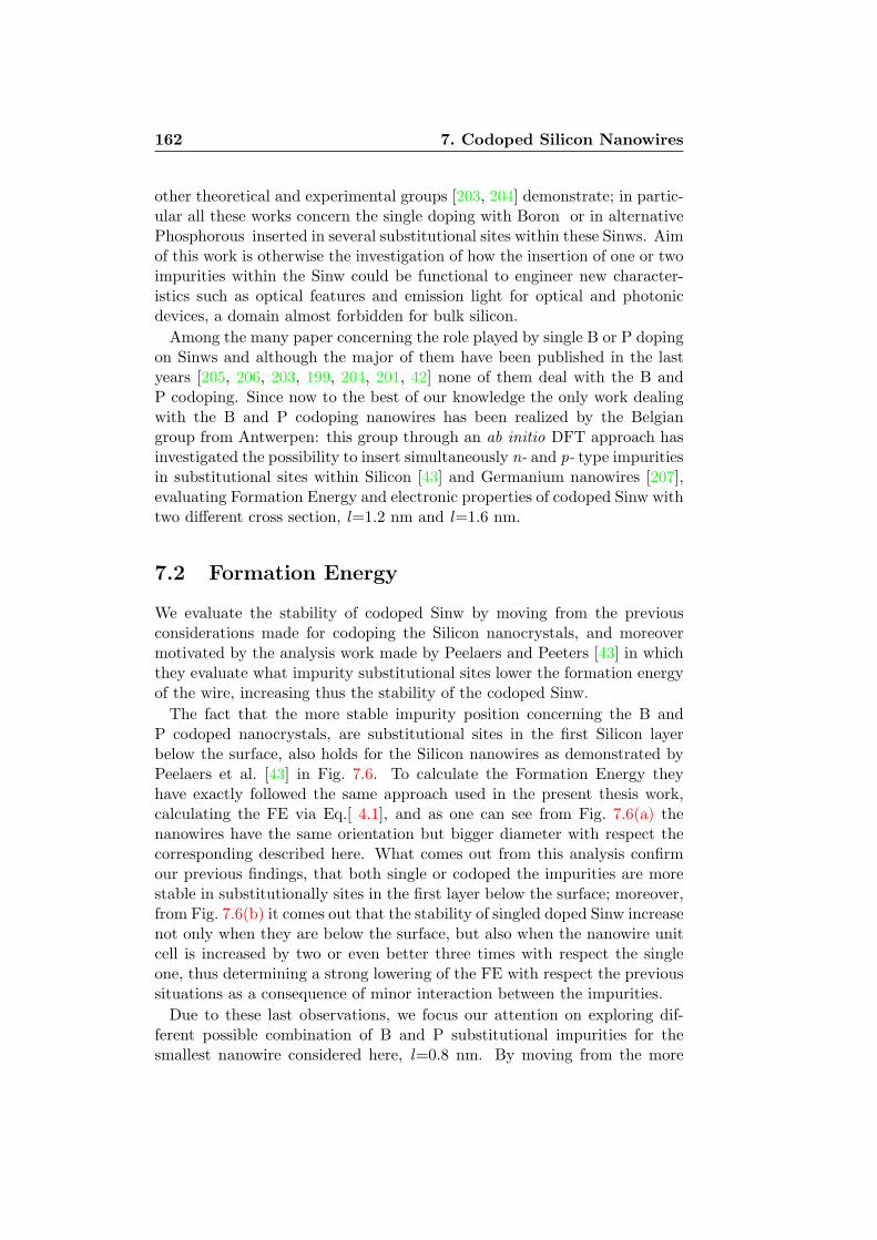
162 7. Codoped Silicon Nanowires
other theoretical and experimental groups [203, 204] demonstrate; in partic-ular all these works concern the single doping with Boron or in alternativePhosphorous inserted in several substitutional sites within these Sinws. Aimof this work is otherwise the investigation of how the insertion of one or twoimpurities within the Sinw could be functional to engineer new character-istics such as optical features and emission light for optical and photonicdevices, a domain almost forbidden for bulk silicon.
Among the many paper concerning the role played by single B or P dopingon Sinws and although the major of them have been published in the lastyears [205, 206, 203, 199, 204, 201, 42] none of them deal with the B andP codoping. Since now to the best of our knowledge the only work dealingwith the B and P codoping nanowires has been realized by the Belgiangroup from Antwerpen: this group through an ab initio DFT approach hasinvestigated the possibility to insert simultaneously n- and p- type impuritiesin substitutional sites within Silicon [43] and Germanium nanowires [207],evaluating Formation Energy and electronic properties of codoped Sinw withtwo different cross section, l=1.2 nm and l=1.6 nm.
7.2 Formation Energy
We evaluate the stability of codoped Sinw by moving from the previousconsiderations made for codoping the Silicon nanocrystals, and moreovermotivated by the analysis work made by Peelaers and Peeters [43] in whichthey evaluate what impurity substitutional sites lower the formation energyof the wire, increasing thus the stability of the codoped Sinw.
The fact that the more stable impurity position concerning the B andP codoped nanocrystals, are substitutional sites in the first Silicon layerbelow the surface, also holds for the Silicon nanowires as demonstrated byPeelaers et al. [43] in Fig. 7.6. To calculate the Formation Energy theyhave exactly followed the same approach used in the present thesis work,calculating the FE via Eq.[ 4.1], and as one can see from Fig. 7.6(a) thenanowires have the same orientation but bigger diameter with respect thecorresponding described here. What comes out from this analysis confirmour previous findings, that both single or codoped the impurities are morestable in substitutionally sites in the first layer below the surface; moreover,from Fig. 7.6(b) it comes out that the stability of singled doped Sinw increasenot only when they are below the surface, but also when the nanowire unitcell is increased by two or even better three times with respect the singleone, thus determining a strong lowering of the FE with respect the previoussituations as a consequence of minor interaction between the impurities.
Due to these last observations, we focus our attention on exploring dif-ferent possible combination of B and P substitutional impurities for thesmallest nanowire considered here, l=0.8 nm. By moving from the more

Formation Energy 163
(a) Single unit cell of Sinw by Peelaers and Peeters. (a) the1.2 nm wire (16 Si atoms and 12 H atoms) corresponds to the0.8 nm Sinw described in the present work. (b) the 1.6 nmwire consists of 4 Si atoms and 20 H atoms.
(b) Formation Energy as a function ofthe position of impurity with reference toFig. 7.6(a). Single doped cases for thebiggest 1.2 nm Sinw.
(c) Formation Energy as a function of the position ofimpurity with reference to Fig. 7.6(a). Codoped casesfor the biggest 1.2 nm Sinw.
Figure 7.6: Figures illustrating the data on the Formation Energies explainedin the work by Peelaers, Peeters et al.[43] on B-P codoping Silicon Nanowire.

164 7. Codoped Silicon Nanowires
stable impurity sites for the single doped cases corresponding to the sub-stitutional sites just below the surface and illustrated in Fig. 7.7 we decide
Top view Wire growth direction [110]
B doped
P doped
Figure 7.7: One unit cell single doped Sinw (l=0.8 nm) with B and P impuritiesin substitutional sites in the first layer below the surface. On the left column isreported the nanowire cross section while on the right column the nanowire isoriented along the [110] growth direction; magenta atom is Boron, dark-brownis Phosphorus.
how to codoped the nanowires. Several impurity configuration have beenexplored in order to bring out how the mutual position of the two simulta-neous impurities in the first layer below the surface affects the stability andthen the electronic structure of the nanowires. In Fig. 7.8 are reported fourdifferent type of configuration for the codoped l=0.8 nm Sinw.
In the first panel the B and P are both subsurface like second neighbors(DBP =4.29 A) while in the second and third panels the impurities are placedlike near neighbors keeping the B fixed in the subsurface layer and puttingthe P atom one time in the center of the Sinw (DBP =1.95 A) and the otherone in a surface substitutional site (DBP =2.17 A). In the fourth panel theB is in a substitutional site at the surface, the P instead in a subsurface sitelike near neighbors as before, and maintaining the same mutual distance asthe previous case (DBP =2.17 A).
Thus, from Table 7.2 where the Formation Energy and the energy gap
Formation Energy 165
Top view Wire growth direction [110]
B,P Ishell
P center-B Ishell
P surf-B Ishell
B surf-P Ishell
Figure 7.8: One unit cell B-P codoped Sinw (l=0.8 nm): several impurityconfiguration are explored (see text for details).

166 7. Codoped Silicon Nanowires
Nanowire DBP Formation Energy Direct Energy Gap(l=0.8 nm) (A) (eV) (eV)
Si15BH12 1.13 1.4Si15PH12 0.66
Si14BPH12
B and P subsurface 4.3 0.41 0.08P center, B subsurface 1.95 0.10 0.63P surface, B subsurface 2.17 -0.05 0.97B surface, P subsurface 2.17 -0.28 1.24
Table 7.2: Formation Energy and Energy Gap (see text) for the single dopedand the codoped (see Fig. 7.8 nanowires (l=0.8 nm)).
for single and codoped Sinw are reported, one can see that as for the Sinc,the single doping is less favored than the codoping, in good agreement withthe previously theoretical prediction in [43]. Nonetheless, what’s result to benew and interesting with respect the work [43], is that for the smallest Sinwwe considered here (l=0.8 nm) the most stable sites for B and P impuritieswere not the subsurface positions. In this cases, infact, the FE is stronglylowered with respect the case in which the two impurities are simultaneouslyin substitutional sites below the surface, where it is 0.41 eV. As from thenumerical values of Table 7.2 and as sketched in Fig. 7.9, the FE movesfrom a small positive value (0.1 eV) when the P atom occupies a Si coresubstitutional site (in Fig. 7.9 position label by 1) to a negative one (-0.05 eV) when the P impurity is substitutionally placed surface site andpassivated by hydrogen (position 1). Furthermore, with respect to this lastconfiguration, when the mutual position of B and P are exchanged (lastpanel of Fig. 7.8), FE becomes again more negative assuming the smallestvalue (-0.28 eV) since now.
Some observations could be done. There’s no linear dependence betweenthe strong decrease of FE from 0.41 eV to -0.28 eV and the B-P impuritydistance, but nevertheless when the mutual distance decreases undera certain value, the stability of the codoped nanowires increases, thusdemonstrating once again that more closed are the n- and p- type dopantsmore the wire gains stability form the formation of a B-P impurity complex.It’s also worth mentioning that the negative FE values found when aP or B atom is passivated at surface with hydrogen are corroboratedby the experimental evidence by the work of Fukata [206, 205] whichdemonstrate how the impurities tend to be substitutionally doped inthe Si core of the nanowires where they can be activated, but also thatwhen the doped Sinw are passivated with hydrogen impurities, Boron in

Formation Energy 167
Figure 7.9: Formation Energy for BP codoped l=0.8 nm Sinw as a functionof the distance between the two impurities. The FE is calculated for each stepof the ”Phosphorus impurity path”: the B impurity (magenta) is frozen in asubsurface site, while the P atom occupies different substitutional sites labelledeach time by 1, 2 or 3. The lines are guide for eyes.

168 7. Codoped Silicon Nanowires
particular, tend to form strong complexes with H, called passivation centers.Moreover, the experimental work [205] confirm that B preferentially segre-gate at the edge boundary region of the Sinw, rather than in the Si core sites.
Moreover the discrepancy between the positive FE value and the one foundin the other paper [43] for the codoped Sinw with impurities in the first layerbelow the surface depends on the different dimension of Sinw considered inthe two cases: here the FE energy has been calculated for the l=0.8 nm Sinw,while in the other work the Sinw take into account has a larger diameter of1.2 nm. Taking into account the larger Sinw with cross section l=1.2 nmcodoped with B and P in subsurface position at a distance of 3.65 A thecorresponding FE results to be -0.28 eV, thus confirming an increase instability when the nanowire cross section increase in well agreement withthe theoretical prediction by Peelaers et al. and moreover demonstratingthat small nanowires are more difficult to codoped than the bigger one, suchas for the Silicon nanocrystals. Supported by the reduction of FE for biggerwire diameter, we can say that codoping impurity in the first layer belowthe surface, as done here, borders more a sort of shell-doping [204] than atraditional doping to insert impurities within the nanowires.
The possibility that the FE of codoped Sinw with subsurface BP decreaseswith the augmentation of the nanowires dimension, could be guess by takinga nanowire unit cell two, three and four times bigger than the one unit cellconsidered in this cases, as shown in Table 7.10. In Table 7.3 are collectedthe FE values for this bigger unit cell nanowires (l=0.8 nm) with BP im-purities kept almost at the same distance in the first subsurface layer foreach situation. As depicted in Fig. 7.10 where bigger unit cell are reported,
Nanowire DBP Formation Energy Direct Energy Gap(l=0.8 nm) (A) (eV) (eV)
Si14BPH12 1 unit cell 4.3 0.41 0.08Si30BPH24 2 unit cell 4.35 -0.15 1.1Si46BPH36 3 unit cell 4.2 -0.6 1.43Si62BPH48 4 unit cell 4.35 -0.64 1.51
Table 7.3: Formation energy and energy gap codoped nanowires (l=0.8 nm)with two, three and four times bigger than the single unit.
increasing the unit cell corresponds to increase the overall number of atomswithin the cell and, furthermore, this translates for the codoped Sinw to adecrease of the concentration of the impurity number with respect the totalnumber of the Silicon atoms within the wire. Thus what comes out is thatfirst codoping big nanowires is easier than codoping smaller one and that alowering of the impurity concentration results in a gain of stability for the

Formation Energy 169
X direction Wire Growth
Cell 2U
Cell 3U
Cell 4U
Figure 7.10: Bigger unit cell nanowires. Cell 2U: double unit cell. Cell 3U:three times unit cell. Cell 4U: four time unit cell.

170 7. Codoped Silicon Nanowires
codoped Sinw.
Electronic Properties 171
7.3 Electronic Properties
The insertion of n- and p- type impurities tends to drastically change thefeatures of the electronic structure of the Silicon nanowires, in a much morepronounced way with respect the Silicon nanocrystals counterpart. Thedopants within the Sinw act as shallow impurities and, as already describedfor the nanocrystals, new electronic states whose character is directly relatedto the valence of the impurity, arise near the band edge. In several previousworks, theoretical and experimental, has been shown and established thatundoped pure Silicon nanowires are semiconductors systems, with a directband gap at the zone center with respect Germanium nanowires and alsobulk Silicon which have indirect gaps. This is due to a quantum confinementeffect of the charge carriers, as for the nanocrystals, but now in the planeorthogonal to the wire axis, determining an opening of the band gap. Withrespect to the nanocrystals, the Sinw present energy band and not discreteenergy levels, due to a quantum confinement effect along only two direction.The particularity of the band energy gap EG of the Silicon nanowires (suchas for the Genw) are two:
- the energy gap decreases monotonically with the increasing of thewire’s diameter;
- the band gap depends strongly on the orientation of the wires: inparticular the [110] orientation gives rise to the smallest energy gapamong all the other, probably because the quantum confinement effectsare much more stronger in [100]- and [111]- oriented wires [190, 191].
The undoped [110] Si16H12 (l=0.8 nm) considered here presents a direct bandgap at the Γ as shown by Fig. 7.11: the DFT-GGA gap is 1.66 eV biggerthan the corresponding Si bulk value, but in really good agreement withother EG from the literature for the same wire diameter and orientation.
As said, the simultaneously insertion of B and P dopants leads to a clearband gap reduction although it retains a minimum gap at Γ like in the pureSinw as depicted in Fig. 7.12. The DFT-GGA band gap of the codopedSinw result to be at Γ 0.08 eV in perfect agreement with the value found inthe work by Peelaers [43].
Moreover taking into account the ”Phosphorus impurity path” depictedabove in Fig. 7.9, it’s interesting to note that as the formation energy tendsto decrease the direct band gap enlarge from 0.08 eV (in the case with thehighest positive FE value) to 0.97 eV (the most stable one) as shown graph-ically from the band structures plots in Fig. 7.13. From Table 7.2 the directband gap increases by an amount of 0.9 eV undergoing from the codopedBP in subsurface sites, to the nanowire with B subsurface and P at surface.

172 7. Codoped Silicon Nanowires
Figure 7.11: Electronic band Structure of the undoped 0.8 nm diameter [110]Si16H12 nanowire in one-dimensional Brillouin zone along the wire axis. Theband gap is direct at the Γ k-point.
Figure 7.12: Electronic band Structure of the 0.8 nm diameter Si[110] nanowiresin one-dimensional Brillouin zone along the wire axis. The black (dashed )lineis related to the undoped wire, the red (solid) line refers to the codoped wire.In the figure the 0 refers to the Fermi Level of the considered wires. Impuritiesare in subsurface position (DBP =4.29 A).

Electronic Properties 173
Figure 7.13: Phosphorous path: electronic band Structure of the codoped0.8 nm diameter Si[110]nanowire with B subsurface and P atom occupyingdifferent sites: P subsurface position, DBP =4.3 A, (red solid line); P at sur-face DBP =2.17 A(green dash-dotted line); P at center DBP =1.95 A(magentadashed line). In the figure the 0 refers to the Fermi Level of the consideredwires.

174 7. Codoped Silicon Nanowires
The band gap behaviour can be understood by looking at the spatiallocalization at the Γ k-point of the Highest Occupied Molecular Orbital(HOMO) and the Lowest Unoccupied Molecular Orbitals (LUMO) withinthe nanowires. In Fig. 7.14, 7.15, 7.16 are shown the square moduluscontour plots, with isosurface corresponding to 20% of the maximun value,for the codoped 0.8 nm codoped wire considered before.
From Fig. 7.14 we can see that the HOMO and LUMO orbitals of un-doped and B or P single doped Sinw present the same features which cameout for the Sinc. Thus HOMO and LUMO are spread all over the Siliconcore cross section of the wire, while, for the single doped Sinw, HOMO ismainly centered on the impurity site, whereas LUMO maintains the samekind of localization of the pure hydrogenated Sinw; this respects the trendhighlighted in the theoretical work by Singh et al. [203] where it’s depictedthe localization of the charge density in n- and p- type single doped Sinwfor different diameters and different surface morphologies, thus confirmingan universal orbital localization behaviour in presence of single impurities.When, instead,the B and P impurities are simultaneously inserted in the firstsilicon layer subsurface, see first column of Fig. 7.15, HOMO and LUMOare localized on the two dopants site respectively, determining as a conse-quence the strong reduction of the band gap at the Brillouin zone center.Nonetheless the localization of the wavefunction square modulus can changein the codoped Sinw according to whose substitutional sites are occupied bythe dopants atoms. In Fig. 7.16 and in the right column of Fig. 7.15 thisvariation of orbital localization is shown for different substitutional site oc-cupied by the Phosphorous atom. When the two impurities are no morecontemporary in subsurface substitutional sites, it changes the spatial lo-calization of HOMO orbital, which results now centered on the Silicon coreof the wire apart from the sites occupied by the P dopant. Furthermore,from Fig. ?? when the two impurities are near neighbors, the LUMO is fo-cused on the B-P complex formed. This behavior can be at the origin ofthe strong reduction in Formation Energy, as a sort of modulation doping ora Boron-Phosphorus linear chain ”decorating” the wire and deeply alteringthe peculiar electronic and thermodynamic features of the undoped Si wire.Thus playing with impurity positions can be a way to modulate, to tunethe electronic structure of the Silicon nanowire. Another way to do thatand here a little bit investigated is what happen when are increased thedimensions of the wire by augmenting the unitary cell. As already reportedby numerical values in Table 7.3 as the dimension of the wire unit cell in-crease, the band gap at Γ of the BP codoped wires tends to increase. Thismonotonic increasing trend is represented in Fig. 7.17, where the direct bandenergy gap is plotted with respect to the different unit cell, that means withrespect to the total number of atoms within each unit cell. The increasingof two, three, fourth times the unit cell correspond physically to reduce thefraction of impurities with respect to the overall number of Silicon atoms,

Electronic Properties 175
Undoped B doped P doped
HOMO top
LUMO top
HOMO wire
LUMO wire
Figure 7.14: HOMO and LUMO square modulus contour plots calculated forundoped and single doped Sinw (l=0.8 nm). Columns: undoped (left); Bsubsurface (middle); P subsurface (right). Horizontal: the [110] top view (firsttwo panels) and the [110] direction view (last two panels) of the HOMO andLUMO orbitals respectively.

176 7. Codoped Silicon Nanowires
BP@Ishell Pcentr-BIsh
HOMO top
LUMO top
HOMO wire
LUMO wire
Figure 7.15: HOMO and LUMO square modulus contour plots calculated forcodoped Sinw (l=0.8 nm). Columns: BP subsurface (left); P at center, B sub-surface (right). Horizontal: the [110] top view (first two panels) and the [110]direction view (last two panels) of the HOMO and LUMO orbitals respectively.
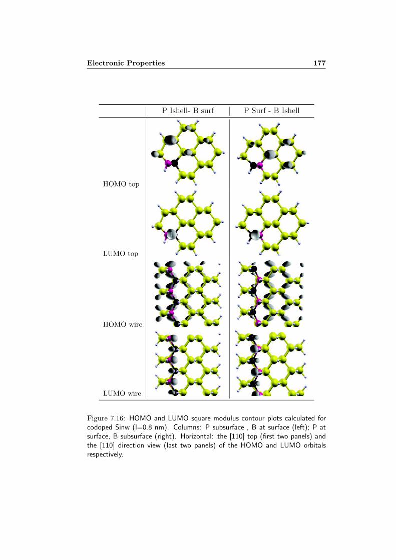
Electronic Properties 177
P Ishell- B surf P Surf - B Ishell
HOMO top
LUMO top
HOMO wire
LUMO wire
Figure 7.16: HOMO and LUMO square modulus contour plots calculated forcodoped Sinw (l=0.8 nm). Columns: P subsurface , B at surface (left); P atsurface, B subsurface (right). Horizontal: the [110] top (first two panels) andthe [110] direction view (last two panels) of the HOMO and LUMO orbitalsrespectively.

178 7. Codoped Silicon Nanowires
thus to a reduction of impurity concentration. Thus from Fig. 7.17 it canbe seen that the band gap increases with the augmentation of the unit cell,thus with the lowering of impurity concentration within the cell, approach-ing asymptotically to the undoped band gap limit represented by the dashedblack line placed at 1.67 eV. Thus we can see that there are many way toinduce with the codoping a modification of the electronic structure of theSilicon nanowire.

Electronic Properties 179
Figure 7.17: DFT-GGA direct band gap calculated at the Γ point with respectSingle Unit cell, double unit cell, third unit cell and fourth unit cell nanowire(l=0.8 nm). The red dotted line is a guide for eyes. The black dashed line is theundoped band energy gap (EG=1.67 eV), constant for each unit cell considered.

180 7. Codoped Silicon Nanowires
7.4 Optical Features
Here we take into account the main results achieved for the optical featuresof the codoped Sinw. We considered the 0.8 nm wire with the four differentunit cell size and 1.2 nm wire with single unit cell. The absorption spectrahave been calculated with the Independent-Particle RPA approach applyingthe simple Fermi Golden rule to estimate the Imaginary part of the dielec-tric function, ε2(ω), as already describe in Section 3 by the Eq.[ 3.11]. InFig 7.18 is reported the optical absorption spectrum for the 0.8 nm undopedand codoped (B and P subsurface) nanowires for a single unit cell, obtainedwithin the single-particle RPA approach. Due to the depolarization effectwhich makes the wire almost transparent in the visible region for light po-larized perpendicularly to the wire axis [190, 191], only the spectrum forlight polarized along the wire axis is shown, together with the spectrumobtained for the corresponding pure Si-nw. The indirect character of thehigh-valence and low-conduction energies states is confirmed here for thepure Si-nw. The codoped Sinw, instead, shows an intense absorption peakin correspondence of the absorption edge at 0.08 eV, due to the high over-lap between the HOMO and LUMO orbitals which are strongly localized onthe Boron and Phosphorous impurity states respectively. The effect of theimpurity states affects deeply the absorption spectrum of the codoped Sinw,revealing a quasi-continuous absorption behaviour typical of a metallic sys-tem; in particular an absorption edge is lower than the related undoped oneand also than the bulk Silicon band gap limit.
Furthermore, the absorption spectra of the other codoped 0.8 nm Sinwhere discussed, reveal a different behaviour.
In Fig. 7.19 and Fig. 7.20 are reported the absorption spectra of the othersingle unit cell codoped Sinw (0.8 nm) which are more stable due to lowerand negative formation energy values. In Fig. 7.19 are reported the absorp-tion spectra of codoped Sinw where P impurity is moved from the centertoward surface and subsurface position, while the B atom is kept fixed in asubsurface site. When P impurity occupies substitutional sites at the centeror at the surface, the absorption thresholds are very close each other locatedat higher values with respect the B-P at Ishell codoped case. Unfortunatelythere are any interesting and appreciable absorption peaks near the absorp-tion edge, indicating that the main absorption features here resemble theindirect character of the undoped Sinw and that in particular the presenceof impurity states do not change so much the spectrum. The same happenwhen one of the two impurities is in a substitutional site at the surface of thenanowire: in Fig.7.20 again there aren’t any intense absorption structuresaround the two absorption edge (blue and cyan line). Thus Phosphorous orBoron in a surface site gives rise to the same effect, very similar to a deple-tion of intense and significative optical transitions in the region below 1.75eV. This effect can be related to the presence of surface states due to the

Optical Features 181
Figure 7.18: The imaginary part of the dielectric function ǫ2(ω) for the [110]oriented Si nanowires (l=0.8 nm). The black solid line is related to the undopedwire, the red solid line refers to the codoped wire, with impurities in the first layerbelow the surface (DBP =4.3 A). The arrows indicate the absorption thresholds.

182 7. Codoped Silicon Nanowires
Figure 7.19: The imaginary part of the dielectric function ǫ2(ω) for the [110]oriented Si nanowires (l=0.8 nm). Red solid line: B and P in subsurface position(DBP =4.3 A). Green solid line: P at center, B subsurface (DBP =1.95 A). Bluesolid line: P at surface, B subsurface (DBP =2.17 A). The arrows indicate theabsorption thresholds.
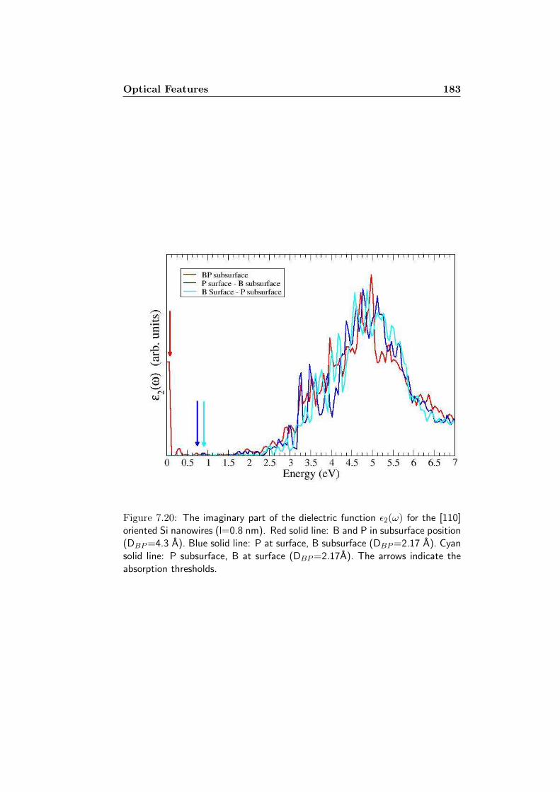
Optical Features 183
Figure 7.20: The imaginary part of the dielectric function ǫ2(ω) for the [110]oriented Si nanowires (l=0.8 nm). Red solid line: B and P in subsurface position(DBP =4.3 A). Blue solid line: P at surface, B subsurface (DBP =2.17 A). Cyansolid line: P subsurface, B at surface (DBP =2.17A). The arrows indicate theabsorption thresholds.
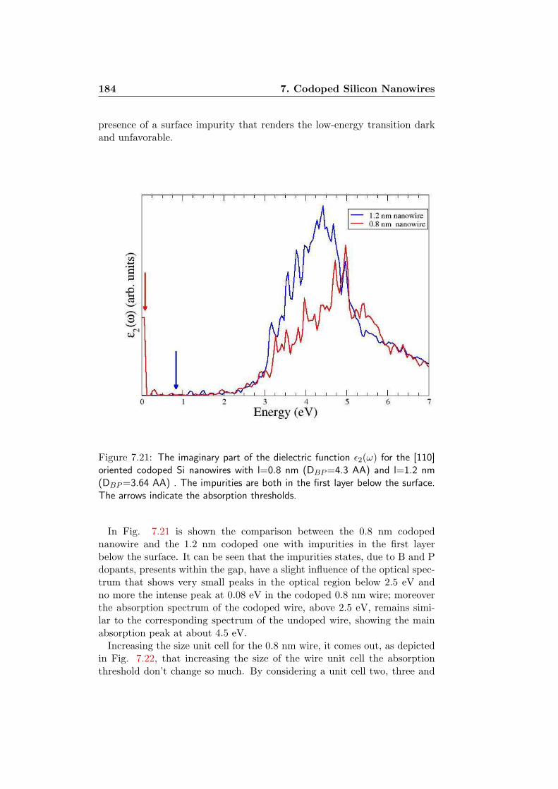
184 7. Codoped Silicon Nanowires
presence of a surface impurity that renders the low-energy transition darkand unfavorable.
Figure 7.21: The imaginary part of the dielectric function ǫ2(ω) for the [110]oriented codoped Si nanowires with l=0.8 nm (DBP =4.3 AA) and l=1.2 nm(DBP =3.64 AA) . The impurities are both in the first layer below the surface.The arrows indicate the absorption thresholds.
In Fig. 7.21 is shown the comparison between the 0.8 nm codopednanowire and the 1.2 nm codoped one with impurities in the first layerbelow the surface. It can be seen that the impurities states, due to B and Pdopants, presents within the gap, have a slight influence of the optical spec-trum that shows very small peaks in the optical region below 2.5 eV andno more the intense peak at 0.08 eV in the codoped 0.8 nm wire; moreoverthe absorption spectrum of the codoped wire, above 2.5 eV, remains simi-lar to the corresponding spectrum of the undoped wire, showing the mainabsorption peak at about 4.5 eV.
Increasing the size unit cell for the 0.8 nm wire, it comes out, as depictedin Fig. 7.22, that increasing the size of the wire unit cell the absorptionthreshold don’t change so much. By considering a unit cell two, three and

Optical Features 185
four times bigger along the wire growth direction [110], the absorption edgetends to be blue shifted towards higher energy with respect to the codopedsingle unit cell nanowire. As before, no intense transition peaks can berecognized for the bigger cell wire below 2 eV. A possible explanation can berelated by considering the variation dopants concentration in each Sinw unitcell: when the unit cell enlarges, the concentration of impurities decreasethus producing an optical response of the codoped Sinw more similar to theresponse of an undoped Sinw.
Figure 7.22: Increasing unit cell size: imaginary part of the dielectric functionǫ2(ω) for the [110] oriented codoped Si nanowires (l=0.8 nm) with B and P inthe first layer below the surface. The arrows indicate the absorption thresholds.

186 7. Codoped Silicon Nanowires
7.4.1 Many Body Absorption Spectra
Here the absorption spectrum of the codoped 0.8 nm wire with B and P insubsurface substitutional position (see top panel in Fig. 7.8) has been calcu-lated with the introduction of the many body effects, namely the self-energyand the excitonic effects [131]. In order to overcome the well known under-estimation of the DFT-GGA band gap (in any local or semilocal approxima-tion for the exchange-correlation potential) with respect to the experiments,the self energy corrections have been calculated within the standard G0W0
approach, leading thus to a better definition of the band gap in terms ofquasi-particle energy:
EQPg = EDFT
g + ∆EGWg
As has been discussed in the literature (see for instance [208]), the use of atruncated Coulomb potential in the many-body calculations, when dealingwith isolated systems in the supercell approach, is really an importantpoint to reach a good accuracy in the final results. In fact, in the case oflow-dimensional non periodic nanostructures, such as the wires, it preventsthe interaction between the replica and allows the use of one-dimensionalk-point samplings. The converged parameters of present GW calculations,performed in a simulation cell with a vacuum region of about 18A, are thefollowing: a uniform one-dimensional grid of 16 k-points, a kinetic-energycut-off of 5 Ry and a sum over the unoccupied states up to about 20 eVabove EF in the correlation part of the self-energy, Σc, while a kinetic-energy cut-off of 10 Ry in the calculation of exchange part of the self-energyΣx.
Before to carry out the calculation for the codoped Si nanowire, we per-formed it in the corresponding undoped nanowire. In this way the GWcorrection to the minimum direct band-gap results to be 1.8 eV. This valueis in a reasonable good agrement with previous self-energy calculations onthe same pure hydrogenated Si-NW [200, 191]. As a general comment, itis important to point out here, that this quasi-particle correction is biggerthan the corresponding value in bulk silicon (about 0.7 eV). Moreover it isnowadays clear that the self-energy corrections tend to decrease toward thebulk value, as the wire diameter is enlarged.Afterwards we performed the same calculation for the codoped Sinw. inthis case the minimum direct gap opens of 1.6 eV with respect to the DFTvalue, showing, at least in the studied case, a slight dependence from thedoping. GW calculations (in the same simulation cell) without the use ofa truncated coulomb potential take to quasi-particle gaps 0.3 smaller, bothfor the pure and for the codoped wire. This difference is clearly due to thelong-range replica interactions which persist when the cylindrical cut-off isnot used, but in any case confirms their slight dependence from the doping.

Optical Features 187
When the quasi-particles states are known, absorption spectrum can becalculated by including also the excitonic effects that take into account theinteraction between an electron and hole pair by resolving the Bethe-Salpeterequation and including only the resonant part of the excitonic hamiltonian.The diagonalization of the excitonic hamiltonian has been performed using1000 G vectors for the screened interaction W, 5000 G for v on 40 bands(half occupied, half empty). In Fig. 7.23 is reported comparison between theimaginary part of the dielectric function of the BP codoped [110] orientedSinw (l=0.8 nm) calculated in the GW quasiparticle approximation without
Figure 7.23: Optical Absorption spectra of [110] oriented codoped Si nanowires(l=0.8 nm) with B and P in the first layer below the surface. Black dashedline quasiparticle (GW) absorption spectrum and red solid line quasiparticle +excitonic effect (BSE+LF) spectrum.
the inclusion of excitonic effects (black dashed line) and by including e-h interaction and local field effects by solving the BSE equation (red solidline), with the inclusion also of the cut-off on the Coulombian potential. Thequasiparticle effect is the opening of the gap that shift toward higher energiesat 1.70 eV the main peak centered around the band edge in the previous IP-

188 7. Codoped Silicon Nanowires
RPA spectrum of Fig. 7.18. When instead excitonic effects are included theelectron-hole interaction tends to close the gap again: the excitonic effecttends again to compensate the GW correction and to cancel partially thequasiparticle effect, thus recovering almost the same peak position aroundthe band gap, now located at 0.28 eV. For this kind of small diameter (0.8nm) wire, the binding energy of the exciton is of the order of 1.3 eV muchbigger then the value for bulk Ge and Si, which is around 60 meV and ofthe same order of magnitude of the binding energies of the correspondingundoped wire, which is 1÷2 eV.

Conclusions
Il sogno di una persona sola rimane unsogno... quello di tante persone insieme e larealta che comincia.
Subcomandante Marcos
The theoretical study performed through ab initio calculations andillustrated in this thesis work represents the summary of my researchactivity achieved during the last three year of PhD fellowship in Modena.The research illustrated is a first study on the effect play by the codopingwith donor and acceptor impurities on Silicon Nanocrystals and Nanowiresand it is part of a bigger field of study on the electronic and opticalproperties of the Silicon Nanostructures with different kind of passivationand surface termination that aim to carry out more information on thepossibility to achieve light and stimulated amplified emission from thesenanosized Silicon based systems.
This basic research thesis work, conduced under the smart and careful su-pervision of Stefano Ossicini and Elena Degoli, is proud to illustrate from atheoretical point of view and for the first time, how the insertion of compen-sated impurities into small Silicon nanostructures can drastically modifiestheir properties contributing thus to shed some more know-how on the pos-sibility to realize sustainable emission of light from Silicon nanostructuresfor optoelectronic applications. To that, briefly are resumed what we haveunderstand about the doping and the codoping in nanosized Silicon:
• Doping nanostructures is not easy to achieve, but possible.The insertion of impurities in Silicon nanostructures in both nanocry-stals and nanowires is difficult. In particular the Formation Energy
189

190 Conclusions
(FE) (Sec. 4.2) carries the information that codoping is easier torealize with respect to single doping; when two impurities are simulta-neously present, due to the charge compensation between the B and Pdopants, in both nanocrystals and nanowires the FE assumes negativevalues that means an increase in the stability of the codoped system.Single doping depends strongly by the systems dimensions since theFE decrease with the size, thus is more difficult to single dope smallnanostructure than the bigger one. Moreover, the most favorable po-sitions for the two impurities (here Boron and Phosphorus) have beendemonstrated to be the substitutional sites in the first Silicon layerbelow the surface, both for the nanocrystals and the nanowires.
- Silicon nanocrystals: due to the charge compensation thecodoping reveals to be almost independent by the nanocrystalssize; moreover the stability increases when the impurities arecloser each other such as second neighbors, in order to increasetheir Coulomb interaction;
- multi-doped nanocrystals: inserting more impurities, thusaugmenting the concentration of dopants within the samenanocrystal lowers more the FE, thus increasing the stability ofthe multi-doped nanocrystals. This should be related to a vari-ation in the screening between the embedded dopants that canincrease their mutual interaction. In particular an even numberof doped compensated impurities leads always to the minor andmore negative value of FE.
• Electronic Properties can be tuned from the correspondingundoped structures counterparts. The simultaneously insertionof compensated donor and acceptor impurities such as Boron andPhosphorus gives rise to the formation of new bound electronic impu-rity states near the band edge, both in nanocrystals than in nanowireswhich deeply alter the overall electronic structure with respect thecorresponding undoped system.
- the energy gap is direct at the Γ k-point and it is strongly reducedby the new impurity levels. The energy gap can be tuned justplaying with the distance between impurities: in same the biggestnanocrystals it shrinks as the B-P distance augments, also belowthe undoped nc value and the bulk Si band gap.
- the energy gap of codoped nanocrystals and nanowires is rigidshifted toward lower energies with respect to the undoped coun-terparts; nevertheless, it maintain a decreasing trend with theenlarging of the size, approaching to the bulk limit.
- both in nanocrystals and nanowires, there is a strong localizationof HOMO and LUMO orbitals on the impurity sites: HOMO is

Conclusions 191
focused on the Boron site, while the LUMO is centered on thePhosphorus site.
- in nanowires, the simultaneously insertion of B and P in smallernanowires considered, gives rise to a strong reduction of the directband gap and to an almost flattening of the band structure aroundthe Γ point;
- in the multi-doped nanocrystals, the addition of more impuritiesdetermines as in codoped nc new impurity states around the va-lence and the conduction edge, with a reduction of the energygap. Nonetheless as the number of inserted impurities increasethe amount of gap shrinking tends almost to saturate toward aconstant value.;
• Promising new optical features close to the experimental out-comes. The insertion of single impurities gives rise to new intenseoptical transitions in low energy range, below the absorption edge ofthe undoped nanocrystals and also below the bulk Silicon band gaplimit. Nevertheless these transitions in single doped nanostructureshave been demonstrated to be almost dark. Indeed, when two simulta-neously compensated impurities are inserted within nanocrystals andnanowires, new ”radiative” not-forbidden transition arise in the ab-sorption and emission spectra.
- Absorption spectra: the IP-RPA calculations show that the ab-sorption edge is strongly lowered with respect to the undopedabsorption spectrum both for nanocrystals and nanowires; in par-ticular increasing the size of the system shifts the absorption onsettoward lower energies, in particular in the visible energy range.Several states around the gap edge are involved in these transi-tions. The many body calculations (performed on the smallestnanocrystal and nanowire among the all considered in the study)confirm this trend also with the inclusion of the local field con-tribution.
- Emission spectra: it has been proposed an efficient scheme tocalculate the emission spectra combining a Constrain DFT ap-proximation with the Green function approach (GW+BSE). Forthe first time in the emission spectrum is take into account alsothe electron-hole interaction, thus leading to treat in a rough butrealistic way the emission spectrum as an estimation of the pho-toluminescence. To that the calculation show an intense Stokesshift between emission and absorption: several intense excitonicpeaks appear in the low energy part of the emission spectra inthe visible range, in really good agreement with the experimen-

192 Conclusions
tal outcomes of Fujii [36, 37], thus confirming the possibility toachieve light emission by codoping Silicon nanocrystals.
Future Perspective
Considering the conclusions achieved an important preliminary basic stepfor a deeper investigation on the role of doping to engineer the electronic andoptical features of Silicon Nanocrystals and Nanowire, here on the followingI present my main expectations for future research outcomes, on many ofwhich theoretical investigation within our group is still begun:
1. to study radiative and non-radiative lifetime of the electron-hole pair recombination in codoped Silicon nanocrystals and nanowiresfrom first principle, including also the many-body effects in terms ofexcitonic hamiltonian and self-energy corrections;
2. to investigate from a first principle approach gain and stimulatedemission in Silicon nanostructures. For the first time a simple ” fourlevel” model will give the possibility to expand book-learning know-ledge about the microscopic origin of optical gain in Silicon Nanocrys-tal, expanding the investigation also to nanowires and to codoped Si-based nanostructures;
3. to study codoped Silicon nanostructures embedded in a Sili-con Dioxide (SiO2) matrix, thus approaching the simulation to theexperimental systems setup;
4. to include in the study of codoped Silicon nanowire the effects of thewire-wire interaction as yet done for undoped Si nanowire, in orderto better simulate the interconnected structure of nanowires by whichthe Porous Silicon is made up and that contain impurities introducedduring the hydrofluoric acid etching process.
Federico Iori
Modena, 6 Novembre 2007

Page 1 - Curriculum vitae of FEDERICO IORI
For more information go to www.cedefop.eu.int/transparency www.europa.eu.int/comm/education/index_en.html www.eurescv-search.com
E U R O P E A N
C U R R I C U L U M V I T A E F O R M A T
PERSONAL INFORMATION
Name FEDERICO IORI
Address VIA IMOLA N° 33 – 41100 MODENA- ITALY
Telephone +39 059 2055283 office - +39 059 302274 home
Fax +39 059 374794 office
E-mail [email protected]
Nationality ITALIAN
Date of birth 29 / 10/ 1979
EDUCATION AND TRAINING
• From January 2005
Up tp December 2007
PhD student
• Name and type of organisation providing education and training
Departement of Physics – INFM –CNR and
National Center on nanoStructures and bioSystem at Surface S3 -
University of Modena and Reggio Emilia
• Principal subjects
PhD thesis on electronic and optical properties of doped Silicon
Nanostructures.
Advisor: Prof. Stefano Ossicini

Page 2 - Curriculum vitae of FEDERICO IORI
For more information go to www.cedefop.eu.int/transparency www.europa.eu.int/comm/education/index_en.html www.eurescv-search.com
• July 2004 Degree in Physics
• Name and type of
organisation providing education and training
University of Modena and Reggio Emilia
• Principal subjects Degree thesis title:
“Ab initio calculations of ground and excited states of silicon nanocrystals”
Advisor Prof. Stefano Ossicini
• July 1998 High School Scientific Diploma
• Name and type of
organisation providing education and training
Scientific Lycee “Alessandro Tassoni”
Modena
• Principal subjects Maths, physics, natural science, chemistry, latin, Italian and English litterature
PERSONAL SKILLS
AND COMPETENCES
MOTHER TONGUE ITALIAN
OTHER LANGUAGES
ENGLISH • Reading skills GOOD
• Writing skills GOOD • Verbal skills GOOD
FRENCH • Reading skills GOOD
• Writing skills ELEMENTARY – NEED A PROPER COURSE • Verbal skills GOOD

Page 3 - Curriculum vitae of FEDERICO IORI
For more information go to www.cedefop.eu.int/transparency www.europa.eu.int/comm/education/index_en.html www.eurescv-search.com
PHD COMPETENCES
I work on ab initio simulations of isolated systems like silicon nanocrystals and nanowires at the nanoscale. Aim of my research is to understand which mechanisms govern the absorption and the emission of light from these nanostructures leading to the possibility to achieve visible amplified light from them for optoelectronic applications. The main idea is to study the role play by simultaneously doping with boron and phosphorus on the electronic structure and on absorption and emission features of the nanocrystals and nanowires. The theoretical investigation on the electronic and ground state properties has been realized within the Density Functional Theory scheme, using ab initio plane wave pseudopotential codes. Moreover to evaluate the optical response of the systems I’ve taken the advantage of numerical codes that permits to calculate absorption and emission spectra going beyond the single particle approach using a many body framework thus taking into account interaction between electrons and holes at the same time.
Knowledge of different Plane wave pseudopotential abinitio codes:
- Espresso Quantum package (PWscf)
- Abinit
- VASP
Knowledge of code for theoretical spectroscopy:
- SELF code
- DP code
- EXC code
Knowledge of Fortran 90 – Latex - Linux main scientific tools

Page 4 - Curriculum vitae of FEDERICO IORI
For more information go to www.cedefop.eu.int/transparency www.europa.eu.int/comm/education/index_en.html www.eurescv-search.com
TEACHING EXPERIENCE
Teaching assistant on Mathematical Methods for Physicist class exercises – 2005-2007
PHD TRAINING PROGRAMM
Courses from 2005 – 2007
a. Strong Correlated Paradigm of Electronic Levels in Solids (Dr. Rontani)
b. Electronic properties of Solids (Dott. Guido Goldoni)
c. Conduct and Misconduct in Sciences (Prof. Stefano Ossicini)
d. Many Body Theory course (Prof. Franca Manghi)
e. Introduction to Montecarlo Theory (Prof. Carlo Jacoboni)
f. Focus group on:
• Nanofriction and tribology (Dr. Andrea Vanossi)
• Scanning probe microscopy (Prof. M. Affronte- A. Alessandrini)
• Many body theory (GW approximation, TDDFT) (Dr. E. Chang – Dr. C.A. Rozzi)
• Electronic and Optoelectronic properties of solids (Prof. Lorenzo Pavesi)
• X-rays Photoemission Spectroscopies (Prof. Petra Rudolf)

Page 5 - Curriculum vitae of FEDERICO IORI
For more information go to www.cedefop.eu.int/transparency www.europa.eu.int/comm/education/index_en.html www.eurescv-search.com
SCHOOLS
• Electronic excitations and spectroscopies : Theory and Codes Laboratoire des Solides Irradies – Ecole Ploytechnique Palaiseau – Paris Cedex, March 2006
• Summer School on Parallel Calculation, High Performance Computation division, CINECA, -Bologna (Italy) , September 5-16, 2005
• Summer School on Computational Materials Science, Materials and Computation Center, University of Illinois, Urbana-Champaign (US) June 13–23, 2005.
CONFERENCES
Poster presentation:
- Nanoquanta Young Researchers’ Meeting (Donostia, May 15-18 2007)
“Novel Optoelectronic Properties of Simultaneously n- and p- doped
Silicon Nanostructures”
- 13th Total Energy Workshop (Trieste, January 10-13, 2007)
“Optical spectra of Doped Silicon Nanocrystals”
Oral presentation:
- The E-MRS 2007 Spring Meeting (Strasbourg, May 28 - June 1, 2007) “Novel Optoelectronic Properties of Simultaneously n- and p- doped Silicon Nanostructures” - 11th NanoQuanta WorkShop Meeting (Houffalize, September 18-24, 2006) “Optical spectra of doped Silicon Nanocrystals” - NanoQuanta Young Researchers’ Meeting (Rome, May 3-8, 2006) “The Nano Doped: Electronic and optical properties of Single and Codoped Silicon Nanocrystals”
VISITS AND EXCHANGE
1) Marie Curie Fellowship from January 2006 to April 2006: Laboratoire des Solides Irradies - Ecole Polytechnique (Palaiseau) advisor Lucia Reining and Christine Giorgetti - abinitio studies of the electronic and optical properties of graphite; 2) Galileo Programm for Cooperation between Italy and France Visiting period June 2007: Laboratoire des Solides Irradies - Ecole Polytechnique (Palaiseau) advisor Lucia Reining and Christine Giorgetti - theoretical spectroscopy of graphite and graphite-like systems with different interplanar stacking;


Full list of publications
1. Federico Iori, Elena Degoli Maurizia Palummo and Stefano Ossicini,Novel Optoelectronic Properties of Simultaneously n- and p- doped Sil-icon Nanostructures, Superlattices and Microstructures (2007) - inpress
2. R. Magri, E. Degoli, Federico Iori, E. Luppi, O. Pulci, S. Ossicini, G.Cantele, F. Trani, D. Ninno, Role of surface passivation and dopingin Silicon Nanocrystals, Journal of Computational Methods in Scienceand Engineering (2007) - to be published
3. Federico Iori, Elena Degoli, Rita Magri, Ivan Marri, G. Cantele, D.Ninno, F. Trani, O. Pulci, Stefano Ossicini, Engineering Silicon Na-nocrystals: Effect of Codoping with Boron and Phosphorus, PhysicalReview B 76, 085302 (2007)
4. Luppi Eleonora, Iori Federico, Magri Rita, Pulci Olivia Ossicini Ste-fano, Degoli Elena, Olevano Valerio, Excitons in silicon nanocrys-tallites: The nature of luminescence, Physical Review B 75, 033303(2007)
5. Stefano Ossicini, E. Degoli, Federico Iori, O. Pulci, G. Cantele, R.Magri, O. Bisi, F. Trani, D. Ninno, Doping in Silicon Nanocryslals,Surface Science 601, 2724-2729 (2007)
6. Stefano Ossicini, O. Bisi, Elena Degoli, I. Marri, Federico Iori,Eleonora Luppi, Rita Magri, Raffaele Poli, G. Cantele, D. Ninno,F. Trani, M . Marsili, O. Pulci, M. Gatti, K. Gaal-Nagy, A. Incze,G. Onida, V. Olevano, First Principle Study of Silicon Nanocrystals:Structural and Electronic Properties, Abosprtion, Emission and Dop-ing, Journal of Nanoscience and Nanotechnology 10, 1-14 (2007)
199

200 Full list of publications
7. Federico Iori, Stefano Ossicini, E. Degoli, E. Luppi, R. Poli, R. Magri,G. Cantele, F. Trani, D. Ninno, Doping in Silicon nanostructures,physica status solidi (a) 204 No. 5, 1312-1317 (2007)
8. Federico Iori, Elena Degoli, Eleonora Luppi, Rita Magri, Ivan Marri,G. Cantele, D. Ninno, F. Trani, and Stefano Ossicini, Doping in Siliconnanocrystals: an ab-initio study of the structural, electronic and opticalproperties, Journal of Luminescence 121, 335-339 (2006)
9. Stefano Ossicini, Federico Iori, Elena Degoli, Eleonora Luppi, RitaMagri, G. Cantele, F. Trani, and D. Ninno, Understanding Doping inSilicon Nanostructures Journal of Selected Topics in Quantum Elec-tronics 12 No 6, 1585 (2006)
10. Stefano Ossicini, Federico Iori, E. Degoli, E. Luppi, R. Magri, G.Cantele, F. Trani, D. Ninno Simultaneously B- and P-doped SiliconNanoclusters: Formation Energies and Electronic Properties AppliedPhysics Letters 87, 173120 (2005)
11. S. Ossicini, Federico Iori, E. Degoli, E. Luppi, R. Magri, G. Cantele,F. Trani, and D. Ninno, P and B single- and co-doped Silicon Nano-crystals: Formation and Activation Energies, Electronic and OpticalProperties, IEEE (Catalog Number 05EX1053) Group IV Photonics,P3 (2005) 1-3.
12. Stefano Ossicini, O. Bisi, G. Cantele, E. Degoli, R. Del Sole,M. Gatti, A. Incze, Federico Iori, E. Luppi, R. Magri, D. Ninno,G.Onida,O.Pulci, Ab-initio Calculations Of The Electronic Propertiesof Hydrogenated and Oxidized Silicon Nanocrystals: Ground and Ex-cited States, Proceedings del XVII Congresso AIV-17, 277-282 (2005).
13. S.Ossicini, E. Degoli, E. Luppi, R. Magri, Federico Iori, G. Cantele, D.Ninno, The structural, electronic and optical properties of silicon nan-oclusters: effect of size, doping and surface passivation, Science andSupercomputing at Cineca - Report 2005 ISBN 88-86037-16-3 Editors:Marco Voli, Patrizia Coluccia CINECA Printed by: Monograf s.r.l

Bibliography
Bibliography
[1] Semiconductor Silicon: The Extraodindary Made Ordinary, volume 22of MRS Bulletin, MRS Bulletin, 1997.
[2] R. Kirchain and L. Kimerling, A roadmap for nanophotonics, NatPhoton 1(6), 303–305 (2007).
[3] L. Kimerling, Silicon Microphotonics, App. Surf. Science 159-160,8–13 (200).
[4] A. Irace, G. Coppola, G. Breglio, and A. Cutolo, Fast silicon-on-siliconoptoelectronic router based on a BMFET device, Selected Topics inQuantum Electronics, IEEE Journal of 6, 14 (2000).
[5] B. Li, Z. Jiang, X. Zhang, X. Wang, J. Wan, G. Li, and E. Liu,SiGe/Si Mach–Zehnder interferometer modulator based on the plasmadispersion effect, Applied Physics Letters 74(15), 2108–2109 (1999).
[6] S. M. Cstak, J. D. Schaub, W. E. Wu, and J. C. Campbell, High-speedmonolithically integrated silicon optical receiver.
[7] G. Masini, L. Colace, and G. Assanto, Si based optoelectronics forcommunications.
[8] S. Winnerl, D. Buca, S. Lenk, C. Buchal, S. Mantl, and D.-X. Xu,MBE grown Si/SiGe undulating layer superlattices for infrared lightdetection.
201

202 Bibliography
[9] S. Ossicini, L. Pavesi, and F. Priolo, Light Emitting Silicon for Mi-crophotonics, volume 194 of Monograph Springer Tracts in ModernPhysics, Springer-Berlin, 2003.
[10] Silicon Photonics, Springer Tracts in Modern Physics, Springer Verlag,New York, 2004, 2003.
[11] L. T. Canham, Silicon quantum wire array fabrication by electro-chemical and chemical dissolution of wafer, Appl. Phys. Lett. 57,1045–1048 (1990).
[12] O. Bisi, S. Ossicini, and L. Pavesi, Porous silicon: a quantum spongestructure for silicon based optoelectronics, Surf. Sci. Rep. (Nether-lands) 38, 1–126 (2000).
[13] A. G. Cullis and L. T. Canham, Visible light emission due to quantumsize effects in highly porous crystalline silicon, Nature 353(6342), 335–338 (1991).
[14] P. D. J. Calcott, K. J. Nash, L. T. Canham, M. J. Kane, and D. Brum-head, Identifications of radiative transitions in highly porous silicon,J. Phys. Condens. Matter. 5, L91–L98 (1993).
[15] L. Pavesi, L. D. Negro, C. Mazzoleni, G. Franzo, and F. Priolo, Opticalgain in silicon nanocrystals, Nature (London) 408, 440–444 (Nov.2000).
[16] C. Garcia, B. Garrido, P. Pellegrino, R. Ferre, J. A. Moreno, J. R.Morante, L. Pavesi, and M. Cazzanelli, Size dependence of lifetimeand absorption cross section of Si nanocrystals embedded in SiO2,Appl. Phys. Lett. 82(10), 1595–1597 (Mar. 2003).
[17] L. D. Negro, M. Cazzanelli, L. Pavesi, S. Ossicini, D. Pacifici,G. Franzo, F. Priolo, and F. Iacona, Dynamics of stimulated emis-sion in silicon nanocrystals, Appl. Phys. Lett. 82(26), 4636–4638(June 2003).
[18] Towards the first silicon laser, NATO Science Series, Kluwer AcademicPublishers, Dordrecht 2003, 2003.
[19] Y. Kanemitsu, K. Suzuki, H. Uto, Y. Masumoto, T. Matsumoto,S. Kyushin, K. Higuchi, and H. Matsumoto, Visible photolumines-cence of silicon-based nanostructures: Porous silicon and small silicon-based clusters, Appl. Phys. Lett. 61(20), 2446–2448 (Nov. 1992).
[20] G. Allan, C. Delerue, and M. Lannoo, Theory of optical propertiesof polysilanes:Comparison with porous silicon, Phys. Rev. B 48(11),7951–7959 (Sept. 1993).
Bibliography 203
[21] W. Wilson, P. F. Szajowski, and L. E. Brus, Quantum confinement insize-selected, surface-oxidized silicon nanocrystals, Science 262(5137),1242–1244 (Nov. 1993).
[22] Z. H. Lu, D. J. Lockwood, and J. Baribeau, Quantum confinementand light emission in SiO2/Si superlattices, Nature (London) 378,258–260 (1996).
[23] J. Ruan, P. M. Fauchet, L. D. Negro, M. Cazzanelli, andL. Pavesi, Stimulated emission in nanocrystalline silicon superlattice,Appl. Phys. Lett. 83(26), 5479–5481 (Dec. 2003).
[24] A. G. Nassiopoulos, S. Grigoropoulos, and D. Papadim-itriou, Electroluminescent device based on silicon nanopillars,Appl. Phys. Lett. 69(15), 2267–2269 (1996).
[25] J. Johnson, H. Yan, R. Schaller, L. Haber, R. Saykally, and P. Yang,Single Nanowire Lasers, Journal of Physical Chemistry B 105(46),11387–11390 (2001).
[26] X. D. Cui, A. Primak, X. Zarate, J. Tomfohr, O. F. Sankey, A. L.Moore, T. A. Moore, D. Gust, G. Harris, and S. M. Lindsay, Re-producible Measurement of Single-Molecule Conductivity, Science294(5542), 571–574 (Oct. 2001).
[27] Y. Cui, Z. Zhong, D. Wang, W. Wang, and C. Lieber, High Perfor-mance Silicon Nanowire Field Effect Transistors, Nano Letters 3(2),149–152 (2003).
[28] C. Delerue, G. Allan, and M. Lannoo, Electron-phonon coupling andoptical transitions for indirect-gap semiconductor nanocrystals, Phys.Rev. B 64(19), 193402 (Oct 2001).
[29] S. Ossicini, O. Bisi, G. Cantele, E. Degoli, R. D. Sole, M. Gatti, A. In-cze, F. Iori, E. Luppi, R. Magri, D. Ninno, G. Onida, and O.Pulci,Ab-initio Calculations Of The Electronic Properties of Hydrogenatedand Oxidized Silicon Nanocrystrals: Ground and Excited States, inProceedings del XVII Congresso AIV-17, pages 277–282, 2005.
[30] C. Delerue, G. Allan, and M. Lannoo, Dimensionality-Dependent Self-Energy Corrections and Exchange-Correlation Potential in Semicon-ductor Nanostructures, Phys. Rev. Lett. 90(7), 076803 (Feb. 2003).
[31] J. C. Vial, A. Bsiesy, F. Gaspard, R. Herino, M. Ligeon, F. Muller,R. Romestain, and R. M. Macfarlane, Mechanisms of visible-lightemission from electro-oxidized porous silicon, Phys. Rev. B 45(24),14171–14176 (Jun 1992).
204 Bibliography
[32] S. Takeoka, M. Fujii, S. Hayashi, K. Yamamoto, and K. Toshikiyo,Control of photoluminescence energy of Si nanocrystals by Ge doping,Journal of Luminescence 87-89, 350–352 (May 2000).
[33] M. Fujii, S. Hayashi, and K. Yamamoto, Photoluminescence from B-doped Si nanocrystals, Journal of Applied Physics 83(12), 7953–7957(1998).
[34] Y. Cui and C. M. Lieber, Functional Nanoscale Electronic Devices As-sembled Using Silicon Nanowire Building Blocks, Science 291(5505),851–853 (2001).
[35] D. D. D. Ma, C. S. Lee, F. C. K. Au, S. Y. Tong, and S. T. Lee,Small-Diameter Silicon Nanowire Surfaces, Science 299(5614), 1874–1877 (2003).
[36] M. Fujii, Y. Yamaguchi, Y. T. K. Ninomiya, and S. Hayashi, Controlof photoluminescence properties of Si nanocrystals by simultaneouslydoping n- and p-type impurities, Appl. Phys. Lett. 85(7), 1158–1160(2004).
[37] M. Fujii, Y. Yamaguchi, Y. Takase, K. Ninomiya, and S. Hayashi,Photoluminescence from impurity codoped and compensated Si nano-crystals, Applied Physics Letters 87(21), 211919 (2005).
[38] M. Fujii, K. Toshikiyo, Y. Takase, Y. Yamaguchi, and S. Hayashi,Below bulk-band-gap photoluminescence at room temperature fromheavily P- and B-doped Si nanocrystals, Journal of Applied Physics94(3), 1990–1995 (2003).
[39] D. Kovalev, H. Heckler, G. Polisski, and F. Koch, Optical Propertiesof Si Nanocrystals, Phys. Status Solidi B 215, 871–932 (1999).
[40] M. Fujii, A. Mimura, S. Hayashi, and K. Yamamoto, Photolumi-nescence from Si nanocrystals dispersed in phosphosilicate glass thinfilms: Improvement of photoluminescence efficiency, Applied PhysicsLetters 75(2), 184–186 (1999).
[41] A. Mimura, M. Fujii, S. Hayashi, D. Kovalev, and F. Koch, Photolu-minescence and free-electron absorption in heavily phosphorus-dopedSi nanocrystals, Phys. Rev. B 62(19), 12625–12627 (Nov 2000).
[42] M.-V. Fernandez-Serra, C. Adessi, and X. Blase, Conductance, SurfaceTraps, and Passivation in Doped Silicon Nanowires, Nano Letters6(12), 2674–2678 (2006).
[43] H. Peelaers, B. Partoens, and F. Peeters, Formation and SegregationEnergies of B and P Doped and BP Codoped Silicon Nanowires, NanoLetters 6(12), 2781–2784 (2006).

Bibliography 205
[44] E. Degoli, G. Cantele, E. Luppi, R. Magri, D. Ninno, O. Bisi, andS. Ossicini, Ab initio structural and electronic properties of hydro-genated silicon nanoclusters in the ground and excited state, PhysicalReview B (Condensed Matter and Materials Physics) 69(15), 155411(2004).
[45] L. E. Ramos, J. Furthmuller, and F. Bechstedt, Reduce influence ofdefects on oxidized Si nanocrystallites, Phys. Rev. B 71(3), 035328(Jan. 2005).
[46] H.-C. Weissker, J. Furthmuller, and F. Bechstedt, Calculation of op-tical properties and density of states for systems with huge unit cells,Phys. Rev. B 64(3), 035105 (July 2001).
[47] H.-C. Weissker, J. Furthmuller, and F. Bechstedt, Structural relax-ation in Si and Ge nanocrystallites: Influence on the electronic andoptical properties, Phys. Rev. B 67(24), 245304 (2003).
[48] A. J. Williamson, J. C. Grossman, R. Q. Hood, A. Puzder,and G. Galli, Quantum Monte Carlo Calculations of Nanos-tructure Optical Gaps: Applications to Silicon Quantum Dots,Phys. Rev. Lett. 89(19), 196803 (Nov. 2002).
[49] J. R. Chelikowsky, L. Kronik, and I. Vasiliev, Time-dependent dentity-functional calculations for the optical spectra of molecules,clusters,and nanocrystals, J. Phys. Condens. Matter. 15, R1517–R1547 (Aug.2003).
[50] D. V. Melnikov and J. R. Chelikowsky, Electron affinities and ioniza-tion energies in Si and Ge nanocrystals, Phys. Rev. B 69(11), 113305(Mar. 2004).
[51] S. Ogut, J. R. Chelikowsky, and S. G. Louie, Quantum Confinementand Optical Gaps in Si Nanocrystals, Phys. Rev. Lett. 79(9), 1770–1773 (Sept. 1997).
[52] G. Allan, C. Delerue, and M. Lannoo, Nature of Luminescent SurfaceStates of Semiconductor Nanocrystallites, Phys. Rev. Lett. 76(16),2961–2964 (Apr. 1996).
[53] J. P. Proot, C. Delerue, and G. Allan, Electronic structure and op-tical properties of silicon crystallites: application to porous silicon,Appl. Phys. Lett. 61(16), 1948–1950 (Appl. Phys. Lett. ).
[54] C. Delerue, G. Allan, and M. Lannoo, Theoretical aspects of theluminescence of porous silicon, Phys. Rev. B 48(15), 11024–11036(Oct. 1993).

206 Bibliography
[55] N. Daldosso, M. Luppi, G. Dalba, L. Pavesi, F. Rocca, F. Priolo,G. Franzo, F. Iacona, E. Degoli, R. Magri, and S. Ossicini, Experi-mental and Theoretical Joint Study on the Electronic and StructuralProperties of Silicon Nanocrystals Embedded in SiO2: Active Role ofthe Interface Region, in Optoelectronics of Group-IV-Based Materials,edited by T.Gregorkiewicz, R. G. Elliman, P. M. Fauchet, and J. A.Hutchby, volume 770 of Mat. Res. Soc. Symp. Proc., pages I6.1.1–I6.1.5, MRS, 2003.
[56] N. Daldosso, M. Luppi, S. Ossicini, E. Degoli, R. Magri, G. Dalba,P. Fornasini, R. Grisenti, F. Rocca, L. Pavesi, S. Boninelli, F. Pri-olo, C. Spinella, and F. Iacona, Role of the interace region on theoptoelectronic properties of silicon nanocrystals embedded in SiO2,Phys. Rev. B 68(8), 085327 (Aug. 2003).
[57] E. Luppi, F. Iori, R. Magri, O. Pulci, S. Ossicini, E. Degoli, and V. Ole-vano, Excitons in silicon nanocrystallites: The nature of luminescence,Physical Review B (Condensed Matter and Materials Physics) 75(3),033303 (2007).
[58] M. Born and J.M. Oppenheimer, Ann. Physik 84, 457 (1927).
[59] D. R. Hartree, Proc. Cambridge Philos. 24, 89 (1928).
[60] V. Fock, Z. Phys. 61, 126 (1930).
[61] G. D. Mahan, Many-particle physics, Plenum, New York, 1981.
[62] L.H. Thomas, Proc. Cambridge Philos. 23, 542 (1927).
[63] E. Fermi, Z. Phys. 48, 73 (1928).
[64] P. A. M. Dirac, Proc. Cambridge Philos. 26, 376 (1930).
[65] P. Hohenberg and W. Kohn, Inhomogeneus Electron Gas,Phys. Rev. 136(3B), B864–B871 (Nov. 1964).
[66] W. Kohn and L. J. Sham, Self-Consistent Equations Including Ex-change and Correlation Effects, Phys. Rev. 140(4A), A1133–A1138(Nov. 1965).
[67] R. M. Dreizler and E. K. U. Gross, Density Functional Theory: AnApproach to the Quantum Many-Body Problem, Springer, 1990.
[68] A. L. Fetter and J. D. Walecka, Quantum theory of many-particlesystems, McGraw-Hill, New York, 1971.

Bibliography 207
[69] R. W. Godby and P. Garcıa-Gonzalez, Density Functional Theoriesand Self-energy Approaches, in A Primer in Density Functional The-ory, edited by C. Fiolhais, F. Nogueira, and M. Marques, LectureNotes in Physics, Springer-Verlag, 2003.
[70] W. Kohn, Nobel Lecture: Electronic structure of matterwave functionsand density functionals, Rev. Mod. Phys. 71(5), 1253–1266 (Oct.1999).
[71] D. M. Ceperley and B. J. Alder, Ground State of the Electron Gas bya Stochastic Method, Phys. Rev. Lett. 45(7), 566–569 (Aug 1980).
[72] J. Jung, P. Garcia-Gonzalez, J. E. Alvarellos, and R. W. Godby, As-sessment of density-functional approximations: Long-range correla-tions and self-interaction effects, Phys. Rev. A 69(5), 052501 (May2004).
[73] S. Ossicini and C. M. Bertoni, Density-functional calculation of atomicstructure with nonlocal exchange and correlation, Phys. Rev. A 31(6),3550–3556 (Jun 1985).
[74] J. P. Perdew, K. Burke, and M. Ernzerhof, Generalized GradientApproximation Made Simple, Phys. Rev. Lett. 77(18), 3865–3868(Oct. 1996).
[75] C. A. Ullrich, U. J. Gossmann, and E. K. U. Gross, Time-dependentoptimized effective potential, Phys. Rev. Lett. 74(6), 872–875 (Feb.1995).
[76] E. Engel, Orbital-Dependent Functionals for the Exchange-Correlation Energy: A Third Generation of Density Functionals,in A Primer in Density Functional Theory, edited by C. Fiolhais,F. Nogueira, and M. Marques, Lecture Notes in Physics, Springer-Verlag, 2003.
[77] G. E. Engel, Linear Response and the Exchange-CorrelationHole within a Screened-Exchange Density Functional Theory,Phys. Rev. Lett. 78(18), 3515–3518 (Aug. 1997).
[78] S. Kummel and J. P. Perdew, Simple Iterative Construction of theOptimized Effective Potential for Orbital Functionals, Including ExactExchange, Phys. Rev. Lett. 90(4), 043004 (Jan. 2003).
[79] J. P. Perdew and A. Zunger, Self-interaction correction to density-functional approximations for many-electron systems, Phys. Rev. B23(10), 5048–5079 (May 1981).

208 Bibliography
[80] U. von Barth and L. Hedin, A local exchange-correlation potential forthe spin polarized case. i, Journal of Physics C: Solid State Physics5(13), 1629–1642 (1972).
[81] O. Gunnarsson and B. I. Lundqvist, Exchange and correlation inatoms, molecules, and solids by the spin-density-functional formalism,Phys. Rev. B 13(10), 4274–4298 (May 1976).
[82] J. P. Perdew and S. Kurth, Density Functionals for Non-relativisticCoulomb Systems in the New Century, in A Primer in Density Func-tional Theory, edited by C. Fiolhais, F. Nogueira, and M. Marques,Lecture Notes in Physics, Springer-Verlag, 2003.
[83] M. Levy and J. P. Perdew, Hellmann-Feynman, virial, and scalingrequisites for the exact universal density functionals. Shape of thecorrelation potential and diamagnetic susceptibility for atoms, Phys.Rev. A 32(4), 2010–2021 (Oct 1985).
[84] S.-K. Ma and K. A. Brueckner, Correlation Energy of an Electron Gaswith a Slowly Varying High Density, Phys. Rev. 165(1), 18–31 (Jan1968).
[85] J. P. Perdew, K. Burke, and Y. Wang, Generalized gradient approx-imation for the exchange-correlation hole of a many-electron system,Phys. Rev. B 54(23), 16533–16539 (Dec 1996).
[86] T. Koopmans, Physica 1, 104 (1933).
[87] J. F. Janak, Phys. Rev. B 18, 7165 (1978).
[88] C.-O.Almbladth and U. von Barth, Exact results for the charge andspin densities, exchange-correlations potentials, and density-functionaleigenvalues, Phys. Rev. B 31(6), 3231–3244 (1985).
[89] J. P. Perdew and M. Levy, Physical Content of the Exact Kohn-Sham Orbital Energies: Band Gap and Derivative Discontinuities,Phys. Rev. Lett. 51(20), 1884–1887 (1983).
[90] L. S. Sham and M. Schluter, Density Functional Theory of the EnergyGap, Phys. Rev. Lett. 51(20), 1888–1891 (Nov. 1983).
[91] J. P. Perdew, R. G. Parr, M. Levy, and J. L. Balduz, Density-functional theory for fractional particle number: derivative discon-tinuities of the energy, Phys. Rev. B 49(23), 1691–1694 (Dec. 1982).
[92] L. J. Sham and M. Schluter, Density-functional theory for the bandgap, Phys. Rev. B 32(6), 3883–3889 (Sept. 1985).

Bibliography 209
[93] M. S. Hybertsen and S. G. Louie, First-Principles Theory of Quasi-particles: Calculation of Band Gaps in Semiconductor and Insulators,Phys. Rev. Lett. 55(13), 1418–1421 (Sept. 1985).
[94] M. S. Hybertsen and S. G. Louie, Electron correlation and the bandgap in ionic crystals, Phys. Rev. B 32(10), 7005–7008 (Nov. 1985).
[95] M. S. Hybertsen and S. G. Louie, Erratum: Electron correlation andthe band gap in ionic crystals, Phys. Rev. B 35(17), 9308 (June 1987).
[96] W. Ku and A. G. Eguiluz, Band-Gap Problem in SemiconductorsRevisited: Effects of Core States and Many-Body Self-Consistency,Phys. Rev. Lett. 89(12), 126401 (Sept. 2002).
[97] M. S. Hybertsen and S. G. Louie, Electron correlation in semi-conductors and insulators: Band gaps and quasiparticle energies,Phys. Rev. B 34(8), 5390–5413 (Oct. 1986).
[98] Landolt and Bornstein, Zahlenwerte und Funktionen aus Naturwis-senschaften und Technik, in Vol. III of Landolt-Bornstein, Springer,New York, 1982.
[99] B. B. G. Baldini, Optical Properties of Na and Li Halide Crystals at55 K, Phys. Status Solidi B 38(1), 325.
[100] R. W. Godby, M. Schluter, and L. J. Sham, Accurate Exchange-Correlation Potential for Silicon and Its Discontinuity on Addition ofan Electron, Phys. Rev. Lett. 56(22), 2415–2418 (June 1986).
[101] R. W. Godby, M. Schluter, and L. J. Sham, Self-energy operatorsand exchange-correlation potentials in semiconductors, Phys. Rev. B37(17), 10159–10175 (June 1988).
[102] R. W. Godby, M. Schluter, and L. J. Sham, Quasiparticle energies inGaAs and AlAs, Phys. Rev. B 35(8), 4170–4171 (Mar 1987).
[103] M. C. Payne, M. P. Teter, D. C. Allan, T. A. Arias, and J. D.Joannopoulos, Iterative minimization techniques for ab initio total-energy calculations: molecular dynamics and conjucate gradients,Rev. Mod. Phys. 64(4), 1045–1097 (Oct. 1992).
[104] W. E. Pickett, Pseudopotential Methods in Condensed Matter Appli-cations, Comp. Phys. Rep. 9, 115.
[105] D. J. Chadi and M. L. Cohen, Special Points in the Brillouin Zone,Phys. Rev. B 8(12), 5747–5753 (Dec 1973).
[106] H. J. Monkhorst and J. D. Pack, Special points for Brillouin-zoneintegrations, Phys. Rev. B 13(12), 5188–5192 (June 1976).

210 Bibliography
[107] E. Fermi, Il Nuovo Cimento11, 157 (1934).
[108] J. C. Phillips and L. Kleinman, New Method for Calculating WaveFunctions in Crystals and Molecules, Phys. Rev. 116(2), 287–294 (Oct1959).
[109] C. Herring, A New Method for Calculating Wave Functions in Crys-tals, Phys. Rev. 57(12), 1169–1177 (Jun 1940).
[110] W. C. Topp and J. J. Hopfield, Chemically Motivated Pseudopotentialfor Sodium, Phys. Rev. B 7(4), 1295–1303 (Feb 1973).
[111] D. R. Hamann, M. Schluter, and C. Chiang, Norm-Conserving Pseu-dopotentials, Phys. Rev. Lett. 43(20), 1494–1497 (Nov 1979).
[112] G. B. Bachelet, D. R. Hamann, and M. Schluter, Pseudopotentialsthat work: From H to Pu, Phys. Rev. B 26(8), 4199–4228 (Oct.1982).
[113] D. Vanderbilt, Soft self-consistent pseudopotentials in a generalizedeigenvalue formalism, Phys. Rev. B 41(11), R7892–R7895 (Apr. 1990).
[114] R. O. Jones and O. Gunnarsson, The density functional formalism,its applications and prospects, Rev. Mod. Phys. 61(3), 689–746 (July1989).
[115] R. W. Godby and I. D. White, Density-Relaxation Part of the Self-Energy, Phys. Rev. Lett. 80(14), 3161–3161 (Apr. 1998).
[116] A. Franceschetti and S. T. Pantelides, Excited-state relaxations andFrank-Condon shift in Si quantum dots, Phys. Rev. B 68(03), 033313(July 2003).
[117] A. Puzder, A. J. Williamson, J. C. Grossman, and G. Galli, Com-putational Studies of the Optical Emission of Silicon Nanocrystals,J. Am. Chem. Soc. 125, 2786–2791 (2003).
[118] F. Mauri and R. Car, Firts-Principles Study of Excitonic Self-Trappingin Diamond, Phys. Rev. Lett. 75(17), 3166–3169 (1995).
[119] H.-C. Weissker, J. Furthmuller, and F. Bechstedt, Excitation Energiesand Radiative Lifetimes of Ge1−xSix Nanocrystals: Alloying VersusConfinement Effects, Phys. Rev. Lett. 90(8), 085501 (Feb 2003).
[120] F. Iori, E. Degoli, R. Magri, I. Marri, G. Cantele, D. Ninno, F. Trani,O. Pulci, and S. Ossicini, Engineering silicon nanocrystals: Theoreticalstudy of the effect of codoping with boron and phosphorus, PhysicalReview B (Condensed Matter and Materials Physics) 76(8), 085302(2007).

Bibliography 211
[121] A. F. Starace, Length and Velocity Formulas in ApproximateOscillator-Strength Calculations, Phys. Rev. A 3(4), 1242–1245 (Apr.1971).
[122] R. D. Sole and R. Girlanda, Optical properties of semiconductorswithin the indipendent-quasiparticle approximation, Phys. Rev. B48(16), 11789–11795 (1993).
[123] J. Tauc, editor, The Optical Properties of Solids, 1966.
[124] N. H. R. Kubo, M. Toda, Statistical Physics II, volume 31 of SpringerSeries in Solid-State Sciences, Springer-Verlag, 1978.
[125] S. L. Adler, Quantum Theory of the Dielectric Constant in Real Solids,Phys. Rev. 126(2), 413–420 (Apr. 1962).
[126] N. Wiser, Dielectric Constant with Local Field Effects Included,Phys. Rev. 129(1), 62–69 (Jan. 1963).
[127] S. Baroni and R. Resta, Ab Initio calculation of the macroscopicdielectric constant, Phys. Rev. B 33(10), 7017–7021 (May 1986).
[128] N. E. Brener, Random-phase-approximation dielectric function fordiamond, with local field effects included, Phys. Rev. B 12(4), 1487–1492 (Aug. 1975).
[129] M. S. Hybertsen and S. G. Louie, Ab initio static dielectric matricesfrom the density-functional approach. I. Formulation and applicationto semiconductors and insulators, Phys. Rev. B 35(11), 5585–5601(Apr. 1987).
[130] M. S. Hybertsen and S. G. Louie, Ab initio static dielectric matricesfrom the density-functional approach. II. Calculation of the screeningresponse in diamond, Si, Ge, and LiCl, Phys. Rev. B 35(11), 5602–5610 (Apr. 1987).
[131] G. Onida, L. Reining, and A. Rubio, Electronic excitations:density-functional versus many-body Green’s-function approaches,Rev. Mod. Phys. 74(2), 601–659 (Apr. 2002).
[132] G. Bussi, Effects of the Electron-Hole Interaction on the Optical Prop-erties of Materials: the Bethe-Salpeter Equation, Phys. Scr. T109,141–151 (2004).
[133] O. V. Dolgov, D. A. Kirzhnits, and E. G. Maksimov, On an admissiblesign of the static dielectric function of matter, Rev. Mod. Phys. 53(1),81–93 (1981).

212 Bibliography
[134] F. J. Dyson, The Radiation Theories of Tomonaga, Schwinger, andFeynman, Phys. Rev. 75(3), 486–502 (Feb 1949).
[135] F. J. Dyson, The S Matrix in Quantum Electrodynamics, Phys. Rev.75(11), 1736–1755 (Jun 1949).
[136] G. F. Roach, Green’s Functions. Introductory Theory with Applica-tions, Van Nostrand Reinhold Co. - London, 1970.
[137] A. E. Taylor and D. C. Clay, Introduction to Functional Analysis,Krieger Publ. Co. Malabar - Florida, 1986.
[138] A. S. Kheifets, V. A. Sashin, M. Vos, E. Weigold, and F. Aryasetiawan,Spectral properties of quasiparticles in silicon: A test of many-bodytheory, Phys. Rev. B 68(23), 233205 (Dec. 2003).
[139] M. S. Hybertsen and S. G. Louie, Spin-orbit splitting in semiconduc-tors and insulators from the ab initio pseudopotential, Phys. Rev. B34(4), 2920–2922 (Aug. 1986).
[140] M. M. Rieger and R. W. Godby, Charge density of semiconductors inthe GW approximation, Phys. Rev. B 58(3), 1343–1348 (July 1998).
[141] P. Bokes and R. W. Godby, Conductance and polarization in quantumjunctions, Phys. Rev. B 69(24), 245420 (2004).
[142] P. Garcıa-Gonzalez and R. W. Godby, GW self-energy calculations forsurfaces and interfaces, Comput. Phys. Commun. 137(1), 108–122(June 2001).
[143] U. von Barth and B. Holm, Self-consistentGW0 results for the electrongas: Fixed screened potential W0 within the random-phase approxi-mation, Phys. Rev. B 54(12), 8411–8419 (Sept. 1996).
[144] B. Holm and U. von Barth, Fully self-consistent GW self-energy ofthe electron gas, Phys. Rev. B 57(4), 2108–2117 (jan 1998).
[145] E. L. Shirley, Optimal basis sets for detailed Brillouin-zone integra-tions, Phys. Rev. B 54(23), 16464–16469 (Dec. 1996).
[146] E. L. Shirley, Many-body effects on bandwidths in ionic, noble gas,and molecular solids, Phys. Rev. B 58(15), 9579–9583 (Oct. 1998).
[147] W.-D. Schone and A. G. Eguiluz, Self-Consistent Calcu-lations of Quasiparticle States in Metals and Semiconductors,Phys. Rev. Lett. 81(8), 1662–1665 (Aug. 1998).
[148] D. Tamme, R. Schepe, and K. Henneberger, Comment on ”Self-Consistent Calculations of Quasiparticle States in Metals and Semi-conductors”, Phys. Rev. Lett. 83(1), 241 (July 1999).

Bibliography 213
[149] A. G. Eguiluz, Eguiluz Replies, Phys. Rev. Lett. 83(1), 242 (July1999).
[150] B. Holm, Total Energies from GW Calculations,Phys. Rev. Lett. 83(4), 788–791 (July 1999).
[151] P. Garcıa-Gonzalez and R. W. Godby, Self-consistent calculation oftotal energies of the electron gas using many-body perturbation theory,Phys. Rev. B 63(7), 075112 (2001).
[152] M. Rohlfing and S. G. Louie, Electron-hole excitations and opticalspectra from first principles, Phys. Rev. B 62(8), 4927–4944 (Aug.2000).
[153] S. Baroni, A. Dal Corso, S. de Gironcoli, and P. Giannozzi, 2001,http://www.pwscf.org.
[154] G. Kresse and J. Furthmuller, Efficient iterative schemesfor ab initio total-energy calculations using a plane-wave ba-sis set, Phys. Rev. B 54(16), 11169–11186 (Oct 1996),http://cms.mpi.univie.ac.at/vasp/.
[155] G. Kresse and J. Furthmuller, Efficiency of ab-initio total energycalculations for metals and semiconductors using a plane-wave basisset, Comp. Mat. Sci. 6(15) (1996).
[156] X. G. et al., First-principles computation of material proper-ties: the ABINIT software project, Comp. Mat. Sci. 25 (2002),http://www.abinit.org/.
[157] SELF code, Andrea Marini, http://www.fisica.uniroma2.it/~self/.
[158] EXC code, Valerio Olevano, http://www.bethe-salpeter.org/.
[159] S. B. Zhang and J. E. Northrup, Chemical potential dependence ofdefect formation energies in GaAs: Application to Ga self-diffusion,Phys. Rev. Lett. 67(17), 2339–2342 (Oct 1991).
[160] G. Cantele, E. Degoli, E. Luppi, R. Magri, D. Ninno, G. Iadonisi, andS. Ossicini, First-principles study of n- and p-doped silicon nanoclus-ters, Physical Review B (Condensed Matter and Materials Physics)72(11), 113303 (2005).
[161] G. M. Dalpian and J. R. Chelikowsky, Self-Purification in Semicon-ductor Nanocrystals, Physical Review Letters 96(22), 226802 (2006).
[162] Q. Xu, J.-W. Luo, S.-S. Li, J.-B. Xia, J. Li, and S.-H. Wei, Chemicaltrends of defect formation in Si quantum dots: The case of group-III and group-V dopants, Physical Review B (Condensed Matter andMaterials Physics) 75(23), 235304 (2007).

214 Bibliography
[163] X. Luo, S. B. Zhang, and S.-H. Wei, Understanding Ultrahigh Doping:The Case of Boron in Silicon, Phys. Rev. Lett. 90(2), 026103 (Jan2003).
[164] L. G. Wang and A. Zunger, Phosphorus and sulphur doping of dia-mond, Phys. Rev. B 66(16), 161202 (Oct 2002).
[165] G. Galli, Solid-state physics: Doping the undopable, Nature 436, 32(2005).
[166] C. Erwin Steven, Z. Lijun, I. Haftel Michael, L. Efros Alexander,A. Kennedy Thomas, and J. Norris David, Doping semiconductornanocrystals, Nature 436, 91 (2005).
[167] M. Lannoo, C. Delerue, and G. Allan, Screening in Semicon-ductor Nanocrystallites and Its Consequence for Porous Silicon,Phys. Rev. Lett. 74(17), 3415–3418 (Apr. 1995).
[168] D. V. Melnikov and J. R. Chelikowsky, Quantum Confinements inPhosphorus-Doped Silicon Nanocrystals, Phys. Rev. Lett. 92(4),046802 (Jan. 2004).
[169] L. E. Ramos, E. Degoli, G. Cantele, S. Ossicini, D. Ninno,J. Furthmuller, and F. Bechstedt, Optical properties of doped Sinanocrystallites, Physical Review B, accepted (2007).
[170] L. E. Ramos, E. Degoli, G. Cantele, S. Ossicini, D. Ninno,J. Furthmuller, and F. Bechstedt, Structural features and electronicproperties of group-III-, group-IV-, and group-V-doped Si nanocrys-tallites, Journal of Physics: Condensed Matter 19(46), 466211 (12pp)(2007).
[171] Z. Zhou, M. L. Steigerwald, R. A. Friesner, and L. Brus, Structuraland chemical trends in doped silicon nanocrystals: First-principlescalculations, Phys. Rev. B 71(24), 245308 (2005).
[172] B. I. Shklovskii and A. L. Efros, Electron Properties of Doped Semi-conductors, Springer-Verlag, 1984.
[173] S. Ossicini, R. Magri, E. Degoli, M. Luppi, and E. Luppi, Surface andconfinement effects on the optical and structural properties of siliconnanocrystals, SPIE Proc. 5222, 1–11 (2003).
[174] I. Vasiliev, S. Ogut, and J. R. Chelikowsky, Ab Initio Ab-sorption Spectra and Optical Gaps in Nanocrystalline Silicon,Phys. Rev. Lett. 86(9), 1813–1816 (2001).

Bibliography 215
[175] Z. Zhou, R. Friesner, and L. Brus, Electronic Structure of 1 to 2 nmDiameter Silicon Core/Shell Nanocrystals: Surface Chemistry, Opti-cal Spectra, Charge Transfer, and Doping, Journal of the AmericanChemical Society 125(50), 15599–15607 (2003).
[176] P. Y. Yu and M. Cardona, Fundamentals of Semiconductors, Springer-Berlin, 2001.
[177] F. Trani, D. Ninno, G. Cantele, G. Iadonisi, K. Hameeuw, E. Degoli,and S. Ossicini, Screening in semiconductor nanocrystals: Ab initioresults and Thomas-Fermi theory, Physical Review B (CondensedMatter and Materials Physics) 73(24), 245430 (2006).
[178] R. M. Wentzcovitch, K. J. Chang, and M. L. Cohen, Electronic andstructural properties of BN and BP, Phys. Rev. B 34(2), 1071–1079(Jul 1986).
[179] F. Bassani and G. P. Parravicini, Electronic States and Optical Tran-sitions in Solids, Pergamon Press, New York, 1975.
[180] W. van Roosbroeck and W. Shockley, Photon-Radiative Recombina-tion of Electrons and Holes in Germanium, Phys. Rev. 94(6), 1558–1560 (Jun 1954).
[181] L. Hedin, New method for calculating the one-particleGreen’s function with application to the electron gas problem,Phys. Rev. 139(3A), A796–A823 (Aug. 1965).
[182] F. Trani, D. Ninno, and G. Iadonisi, Role of local fields in the opticalproperties of silicon nanocrystals using the tight binding approach,Physical Review B (Condensed Matter and Materials Physics) 75(3),033312 (2007).
[183] F. Trani, D. Ninno, and G. Iadonisi, Tight-binding formulation of thedielectric response in semiconductor nanocrystals, Physical Review B(Condensed Matter and Materials Physics) 76(8), 085326 (2007).
[184] O. Boyraz and B. Jalali, Demonstration of a silicon Raman laser, Opt.Express 12(21), 5269–5273 (2004).
[185] F. Iori, E. Degoli, E. Luppi, R. Magri, I. Marri, G. Cantele, D. Ninno,F. Trani, and S. Ossicini, Doping in silicon nanocrystals: An ab initiostudy of the structural, electronic and optical properties, J. Lumin.121, 335–339 (Sept 2006).
[186] M. Hirao, in Microcrystalline and Nanocrystalline Semiconductors,edited by L. Brus, M. Hirose, R. W. Collins, F. Koch, and C. C. Tsai,volume 358 of Mat. Res. Soc. Symp. Proc., MRS, 1995.
216 Bibliography
[187] C. Delerue, M. Lannoo, and G. Allan, Excitonic and Quasi ParticleGaps in Si Nanocrystals, Phys. Rev. Lett. 84(11), 2457–2460 (Mar.2000).
[188] C. Spataru, S. Ismail-Beigi, L. Benedict, and S. Louie, Quasiparti-cle energies, excitonic effects and optical absorption spectra of small-diameter single-walled carbon nanotubes, Appl. Phys. A 78(8), 1129–1136 (May 2004).
[189] E. Chang, G. Bussi, A. Ruini, and E. Molinari, Excitonsin Carbon Nanotubes: An Ab Initio Symmetry-Based Approach,Phys. Rev. Lett. 92(19), 196401 (May 2004).
[190] M. Bruno, M. Palummo, A. Marini, R. D. Sole, V. Olevano, A. N.Kholod, and S. Ossicini, Excitons in germanium nanowires: Quan-tum confinement, orientation, and anisotropy effects within a first-principles approach, Phys. Rev. B 72(15), 153310 (2005).
[191] M. Bruno, M. Palummo, A. Marini, R. D. Sole, and S. Ossicini,From Si Nanowires to Porous Silicon: The Role of Excitonic Effects,Phys. Rev. Lett. 98, 036807 (jan 2007).
[192] L. Vina and M. Cardona, Effect of heavy doping on the optical prop-erties and the band structure of silicon, Phys. Rev. B 29, 6739–6751(Jun 1984).
[193] A. Selloni and S. T. Pantelides, Electronic Structure and Spectra ofHeavily Doped n-Type Silicon, Phys. Rev. Lett. 49(8), 586–589 (Aug1982).
[194] J. Wagner, Photluminescence and excitation spectroscopy in heavilydoped n- and p-type silicon, Phys. Rev. B 29, 2002–2009 (Feb 1984).
[195] Y. Z. Miguel Levy, P. Y. Yu and M. P. Sarachik, Photluminescence ofheavily doped, compensated Si:P,B, Phys. Rev. B 49(3).
[196] K. Thompson, J. H. Booske, D. J. Larson, and T. F. Kelly, Three-dimensional atom mapping of dopants in Si nanostructures, AppliedPhysics Letters 87, 52108–52110 (2005).
[197] F. Buda, J. Kohanoff, and M. Parinello, Optical Properties of PorousSilicon: A First-Principles Study, Phys. Rev. Lett. 69(8), 1272–1275(Aug. 1992).
[198] A. J. Read, R. J. Needs, K. J. Nash, L. T. Canham, P. D. J. Calcott,and A. Qteish, First-principles calculations of the electronic propertiesof silicon quantum wires, Phys. Rev. Lett. 69(8), 1232–1235 (Aug1992).

Bibliography 217
[199] R. Rurali and N. Lorente, Metallic and Semimetallic Silicon ¡100¿Nanowires, Physical Review Letters 94(2), 026805 (2005).
[200] X. Zhao, Y. Liu, S. Inoue, T. Suzuki, R. O. Jones, and Y. Ando, Small-est Carbon Nanotube Is 3 Ain Diameter, Phys. Rev. Lett. 92(12),125502 (Mar. 2004).
[201] M. V. Fernandez-Serra, C. Adessi, and X. Blase, Surface Segrega-tion and Backscattering in Doped Silicon Nanowires, Physical ReviewLetters 96(16), 166805 (2006).
[202] A. B. Filonov, G. V. Petrov, V. A. Novikov, and V. E. Borisenko,Orientation effect in electronic properties of silicon wires, AppliedPhysics Letters 67(8), 1090–1091 (1995).
[203] A. Singh, V. Kumar, R. Note, and Y. Kawazoe, Effects of Morphol-ogy and Doping on the Electronic and Structural Properties of Hydro-genated Silicon Nanowires, Nano Letters 6(5), 920–925 (2006).
[204] J. Zhong and G. Stocks, Localization/Quasi-Delocalization Transi-tions and Quasi-Mobility-Edges in Shell-Doped Nanowires, Nano Let-ters 6(1), 128–132 (2006).
[205] N. Fukata, J. Chen, T. Sekiguchi, N. Okada, K. Murakami, T. Tsu-rui, and S. Ito, Doping and hydrogen passivation of boron in sili-con nanowires synthesized by laser ablation, Applied Physics Letters89(20), 203109 (2006).
[206] N. Fukata, J. Chen, T. Sekiguchi, S. Matsushita, T. Oshima,N. Uchida, K. Murakami, T. Tsurui, and S. Ito, Phosphorus dopingand hydrogen passivation of donors and defects in silicon nanowiressynthesized by laser ablation, Applied Physics Letters 90(15), 153117(2007).
[207] H. Peelaers, B. Partoens, and F. M. Peeters, Properties of B and Pdoped Ge nanowires, Applied Physics Letters 90(26), 263103 (2007).
[208] C. A. Rozzi, D. Varsano, A. Marini, E. K. U. Gross, and A. Rubio, Ex-act Coulomb cutoff technique for supercell calculations, Phys. Rev. B73(20), 205119 (2006).


Ringraziamenti
Con l’ ultima pagina di questa tesi, dopo tre anni intensi di dottoratotrascorsi qui a Modena, si apre un nuovo capitolo. Un capitolo che quasisicuramente sara all’ estero, lontano dall’ Italia e dalla mia citta ma chesenza dubbio contribuira ad arricchirmi e a farmi crescere. Durante questitre anni ho avuto la fortuna di vivere situazioni completamente nuove in cuimai mi sarei visto come attore protagonista, di ritrovarmi in luoghi stranierima al tempo stesso resi familiari dal contatto con persone nuove diverseda me con cui confrontarmi. Ho iniziato davvero a ”vedere il mondo”, nonsolo attraverso gli occhi della Fisica, ma anche attraverso gli occhi dellepersone che ”fanno la fisica”. Il mondo rappresentato dalla mia piccolacitta, sembra banale a dirlo, ma e realmente solo una minuscola, sebbenimportante, parte di cio che mi circonda. Tutte queste magnifiche edimportanti esperienze le devo al mio gruppo di lavoro a Modena che mi haospitato e accolto prima per la tesi di laurea, quindi anche ”sopportato” neitre anni successivi per svolgere la mia tesi di dottorato. Dire semplicementegrazie puo sembrare riduttivo ma la semplicita della parola racchiude tuttala mia gratitudine ed affetto per il prof. Stefano Ossicini: perche mi hafatto da guida nel campo della fisica del Silicio!! con grande professionalitaed onesta, perche riesce sempre ad accompagnare la serieta sul lavoro nonsolo ad una profonda sensibilta ed umanita nei rapporti personali, ma anchead una accattivante curiosita per il mondo attorno, scienza, fatti e persone.Suoi sono gli incoraggiamenti e sue le opportunita offerte attraverso i tantiprogetti scritti che mi hanno consentito davvero di crescere, di affacciarmialla vita. A Stefano va tutto il mio affetto e la mia grande stima di cuore.Il mio grazie e per Elena che mi ha sempre supportato come ”capo piccolo”ma anche come amica; per Ivan con cui si ride, si discute, si parla difotografia, di politica, di precarieta (sic). Grazie a Roberto per la cordialita
219

220
sempre dimostrata e gli pseudo fatti e l’appoggio e le chiacchere! Vi vogliobene come ad una famiglia.Un grazie sentito per le persone con cui ho avuto la fortuna di lavorareinsieme e che hanno davvero contribuito in modo prezioso al mio lavoro ditesi, Olivia e Maurizia a Roma e Giovanni a Napoli. A Lucia e Christineper la pazienza con i ”fiori” e per la meravigliosa possibilita offerta per ilprossimo postdoc in Paris. C’est tres chic!
Voglio poi qui ricordare le altre persone che mi hanno fatto stare bene inquesti anni al Dipartimento di Fisica, che hanno colorato le giornate davantial computer o durante le conferenze. I miei compagni di merende, Lorenzoed Enzo, (pure la rima ho fatto!) e Deborah e Valentina che condividono lostudio con me. Vi debbo tanto. Tutti gli altri ragazzi che ho conosciuto inquesti 3 anni, alcuni sono ormai lontani da Modena (ma ci ricontreremo peril mondo) altri sono ancora qui: Cando (sempre vicino da una vita, anche sele strade si allontanano il filo rosso non si spezzera), Stefania, Diego, Ghiro,Benedetta (one dollar one beer!) e Andrea (la strana coppia?!), David,Daniele, Andrea Ferretti, i ”tritoni” Giulio-Emiliano-Marcello (tovaric!),Gianmarco e i mitici bitter a mezzanotte allo Juta, la punta d’attacodella squadra, brasileira Rosangela, Valerio, Andrea Vanossi, Davide, Elisae MariaGrazia, Layla e Francesco e Marco, Maddalena, Max. Quanterisate...si perche qui ho trovato amici cordiali, carini e gentili, e questo sarail piun bel ricordo che porto con me nel salutarvi tutti.
A coloro che sono a Parigi e che presto raggiungero, Eleonora e Matteo,l’amicizia e il calore che mi avete trasmesso, lo sapete, rimangono un puntosaldo e fermo. A bien tot!
Concludo dedicando questo lavoro alla mia famiglia, alle persone che piumi sono state vicino e che piu mi stanno amando. La mamma e il papa,Gisella e Umberto, che mi hanno assecondato e incoraggiato in tutte lescelte e in tutte le esperienze, lungimiranti e pieni di fiducia, che mi hannoe mi sostengono senza cedimenti, come hanno fatto i miei nonni, Benilde eGino in tutti gli anni preziosi trascorsi assieme. Vi abbraccio. A Francesca,che non solo ha pensato bene di condividere la fisica con me e pure i passidella vita! Che si dimostra una persona speciale anche nelle scelte difficilied impegnative da me prese. Con affetto e riconoscenza.
A tutte le persone che mi hanno accompagnato fino a qui con affetto.A tutte quelle che mi accompagneranno.
Federico