energy-e cient architectures based on stt-mram
TRANSCRIPT

Energy-Efficient Architectures
Based on STT-MRAM
by
Xiaochen Guo
Submitted in Partial Fulfillment of the
Requirements of the Degree
Doctor of Philosophy
Supervised by
Professor Engin Ipek
Department of Electrical and Computer Engineering
Arts, Sciences and Engineering
Edmund A. Hajim School of Engineering and Applied Sciences
University of Rochester
Rochester, New York
2015
ii
Biographical Sketch
The author graduated from Beihang University, Beijing, China with a Bachelor
of Science degree in Computer Science and Engineering, in 2009. She received her
Master of Science degree in Electrical and Computer Engineering from the University
of Rochester, Rochester, NY, in 2011. She continued to pursue a doctoral degree
in Electrical and Computer Engineering at the University of Rochester under the
direction of Professor Engin Ipek. Her dissertation research leverages resistive mem-
ories to build energy-efficient processors, memory systems, and accelerators. She was
awarded the IBM Ph.D. Fellowship twice, in 2012 and 2014. She interned at Samsung
Research America, San Jose, CA, in 2011, and IBM T. J. Watson Research Center,
Yorktown Heights, NY, in 2012 and 2013.
The following publications were a result of the work conducted during doctoral
study:
• Xiaochen Guo, Mahdi Nazm Bojnordi, Qing Guo, and Engin Ipek, “Sanitizer:
Mitigating the Impact of Expensive ECC Checks in STT-MRAM based Main
Memories,” submitted to the 48th International Symposium on Microarchitec-
ture.
• Shibo Wang, Mahdi Nazm Bojnordi, Xiaochen Guo, and Engin Ipek, “Con-
tent Aware Refresh,” submitted to the 48th International Symposium on Mi-
croarchitecture.
• Qing Guo, Xiaochen Guo, Yuxin Bai, Ravi Patel, Engin Ipek, and Eby G.
Friedman, “Resistive TCAM Systems for Data-intensive Computing,” to apear
in IEEE Micro Special Issue on Alternative Computing Designs & Technologies,
2015.
• Ravi Patel, Xiaochen Guo, Qing Guo, Engin Ipek, and Eby G. Friedman,
“Reducing Switching Latency and Energy in STT-MRAM Caches with Field-
Assisted Writing”, to appear in IEEE Transactions on Very Large Scale Inte-
gration (VLSI) Systems, 2015.

iii
• Isaac Richter, Kamil Pas, Xiaochen Guo, Ravi Patel, Ji Liu, Engin Ipek, and
Eby G. Friedman, “Memristive Accelerator for Extreme Scale Linear Solvers,” in
Proceedings of the Government Microcircuit Applications & Critical Technology
Conference, St. Louis, MO, March 2015.
• Engin Ipek, Qing Guo, Xiaochen Guo, and Yuxin Bai,“Resistive Memories
in Associative Computing,” Emerging Memory Technologies: Design, Architec-
ture, and Applications, Yuan Xie (Editor), Springer, July 2013.
• Qing Guo, Xiaochen Guo, Ravi Patel, Engin Ipek, and Eby G. Friedman,
“AC-DIMM: Associative Computing with STT-MRAM,” in Proceedings of the
40th International Symposium on Computer Architecture, Tel-Aviv, Israel, June
2013.
• Qing Guo, Xiaochen Guo, Yuxin Bai, and Engin Ipek, “A Resistive TCAM
Accelerator for Data Intensive Computing,” in Proceedings of the 44th Interna-
tional Symposium on Microarchitecture, Porto Alegre, Brazil, December 2011.
• Xiaochen Guo, Engin Ipek, and Tolga Soyata, “Resistive Computation: Avoid-
ing the Power Wall with Low-Leakage, STT-MRAM Based Computing,” in
Proceedings of the 37th International Symposium on Computer Architecture,
Saint-Malo, France, June 2010.

iv
Acknowledgements
First and foremost, I would like to thank my advisor Prof. Engin Ipek for his
tremendous help and inspiration during these six years. Engin has been a great
teacher, mentor, and friend to me, who has always believed in me more than I have.
I am thankful to Prof. Michael Huang, without whom I would not have come to the
University of Rochester. I would also like to acknowledge NSF, IBM Research, and
Samsung for providing financial support during my graduate studies.
I want to give my grateful and sincere thanks to Prof. Eby Friedman, Prof.
Sandhya Dwarkadas, and Dr. Pradip Bose for serving on my thesis committee and
providing helpful feedback. I appreciate all of the effort that Prof. Chen Ding put in
as the Chair for my defense. I would also like to thank Dr. Tolga Soyata for providing
circuit simulation results for the STT-MRAM based microprocessor work.
I am grateful to my mentors Dr. Hillery Hunter, Dr. Pradip Bose, Dr. Alper
Buyuktosunoglu, Dr. Viji Srinivasan, and Dr. Jude Rivers at IBM research, who
helped me become an independent researcher.
I have been fortunate to collaborate with excellent colleagues in the ECE and
CS departments. I would like to thank Ravi Patel, Mahdi Nazm Bojnordi, Qing
Guo, Yanwei Song, Yuxin Bai, Shibo Wang, Benjamin Feinberg, Isaac Richter, and
Mohammad Kazemi for their help and support.
I would like to give my special thanks to my family and friends for their love,
support, and encouragement.

v
Abstract
As CMOS technology scales to smaller dimensions, leakage concerns are starting
to limit microprocessor performance growth. To keep dynamic power constant across
process generations, traditional MOSFET scaling theory prescribes reducing supply
and threshold voltages in proportion to device dimensions, a practice that induces an
exponential increase in subthreshold leakage. As a result, leakage power has become
comparable to dynamic power in current-generation processes, and will soon exceed
it in magnitude if voltages are scaled down any further.
The rise in sub-threshold leakage also has an adverse effect on the scaling of
semiconductor memories. DRAM density scaling has become increasingly difficult
due to the challenges in maintaining a sufficiently high storage capacitance and a
sufficiently low leakage current at nanoscale feature sizes. Non-volatile memories
(NVMs) have drawn significant attention as potential DRAM replacements because
they represent information using resistance rather than electrical charge. Spin-torque
transfer magnetoresistive RAM (STT-MRAM) is one of the most promising NVM
technologies due to its low write energy, high speed, and high endurance.
This dissertation presents a new class of energy-efficient processor and memory ar-
chitectures based on STT-MRAM. By implementing much of the on-chip storage and
combinational logic using leakage-resistant, scalable RAM blocks and lookup tables,
and by carefully re-architecting the pipeline, an STT-MRAM based implementation
of an eight-core Sun Niagara-like processor reduces chip-wide power dissipation by
1.7× and leakage power by 2.1× at the 32nm technology node, while maintaining
93% of the system throughput of a CMOS-based design.
A new memory architecture, Sanitizer, is introduced to make STT-MRAM a vi-
able DRAM replacement for main memory. Sanitizer addresses retention errors, one
of the most critical scaling problems of STT-MRAM. As the size of the storage el-
ement within an STT-MRAM cell decreases with technology scaling, STT-MRAM
retention errors are expected to become more frequent, which will require multi-bit
error-correcting code (ECC) and periodic scrubbing mechanisms. Sanitizer mitigates
the performance and energy overheads of ECC and scrubbing in future STT-MRAM

vi
based main memories by anticipating the memory regions that will be accessed in
the near future and scrubbing them in advance. It improves performance by 1.22×and reduces end-to-end system energy by 22% over a baseline STT-MRAM system
at 22nm.

vii
Contributors and Funding Sources
This work was supported by a dissertation committee consisting of Professors En-
gin Ipek (advisor) and Eby Friedman of the Department of Electrical and Computer
Engineering, Professor Sandhya Dwarkadas of the Computer Science Department,
and Dr. Pradip Bose from IBM Research. The committee was chaired by Professor
Chen Ding from the Computer Science Department. The following chapters of this
dissertation proposal were jointly produced, and were funded by multiple sources.
My participation and contributions to the research as well as funding sources are as
follows.
I am the primary author of all of the chapters. For Chapter 3, I collaborated with
Dr. Tolga Soyata and Prof. Engin Ipek. Tolga Soyata provided circuit simulation
results for the STT-MRAM based lookup table. The work described in Chapter 3
was published in the proceedings of the 37th International Symposium on Computer
Architecture, and was supported by a National Science Foundation CAREER award.
For Chapter 4, I collaborated with Mahdi Nazm Borjnordi, Qing Guo, and Prof.
Engin Ipek. Mahdi Nazm Borjnordi performed the design space exploration of the
ECC logic design. Qing Guo provided power calculations for the system using McPAT.
The work described in Chapter 4 was supported by an IBM Ph.D. Fellowship.

viii
Table of Contents
List of Tables xi
List of Figures xiii
1 Introduction 1
2 Background and Motivation 4
2.1 Technology Scaling Challenges . . . . . . . . . . . . . . . . . . . . . . 4
2.1.1 Constant Voltage Scaling . . . . . . . . . . . . . . . . . . . . . 5
2.1.2 Constant Electrical Field Scaling . . . . . . . . . . . . . . . . 8
2.1.3 Multicore Scaling . . . . . . . . . . . . . . . . . . . . . . . . . 9
2.2 Resistive Memory Technologies . . . . . . . . . . . . . . . . . . . . . 10
2.2.1 Spin-Torque Transfer Magnetoresistive RAM
(STT-MRAM) . . . . . . . . . . . . . . . . . . . . . . . . . . 12
2.2.2 Phase Change Memory (PCM) . . . . . . . . . . . . . . . . . 14
2.2.3 Resistive RAM (RRAM) . . . . . . . . . . . . . . . . . . . . . 16
3 STT-MRAM based Microprocessors 18
3.1 Background for Resistive Computation . . . . . . . . . . . . . . . . . 19
3.1.1 1T-1MTJ STT-MRAM Cell . . . . . . . . . . . . . . . . . . . 19
3.1.2 Lookup-Table Based Computing . . . . . . . . . . . . . . . . . 23
3.2 Fundamental Building Blocks . . . . . . . . . . . . . . . . . . . . . . 24
3.2.1 RAM Arrays . . . . . . . . . . . . . . . . . . . . . . . . . . . 25
3.2.2 Lookup Tables . . . . . . . . . . . . . . . . . . . . . . . . . . 33
ix
3.3 Structure and Operation of An STT-MRAM based CMT Pipeline . . 44
3.3.1 Instruction Fetch . . . . . . . . . . . . . . . . . . . . . . . . . 46
3.3.2 Predecode . . . . . . . . . . . . . . . . . . . . . . . . . . . . . 50
3.3.3 Thread Select . . . . . . . . . . . . . . . . . . . . . . . . . . . 51
3.3.4 Decode . . . . . . . . . . . . . . . . . . . . . . . . . . . . . . . 53
3.3.5 Execute . . . . . . . . . . . . . . . . . . . . . . . . . . . . . . 55
3.3.6 Memory . . . . . . . . . . . . . . . . . . . . . . . . . . . . . . 59
3.3.7 Write Back . . . . . . . . . . . . . . . . . . . . . . . . . . . . 64
3.4 Experimental Setup . . . . . . . . . . . . . . . . . . . . . . . . . . . . 65
3.4.1 Architecture . . . . . . . . . . . . . . . . . . . . . . . . . . . . 65
3.4.2 Circuit . . . . . . . . . . . . . . . . . . . . . . . . . . . . . . . 67
3.4.3 Applications . . . . . . . . . . . . . . . . . . . . . . . . . . . . 67
3.5 Evaluation . . . . . . . . . . . . . . . . . . . . . . . . . . . . . . . . . 67
3.5.1 Performance . . . . . . . . . . . . . . . . . . . . . . . . . . . . 68
3.5.2 Power . . . . . . . . . . . . . . . . . . . . . . . . . . . . . . . 70
3.6 Summary . . . . . . . . . . . . . . . . . . . . . . . . . . . . . . . . . 72
4 STT-MRAM based Main Memories 74
4.1 Background for Sanitizer . . . . . . . . . . . . . . . . . . . . . . . . . 77
4.1.1 DRAM Error Protection . . . . . . . . . . . . . . . . . . . . . 77
4.1.2 STT-MRAM Reliability . . . . . . . . . . . . . . . . . . . . . 80
4.1.3 Reliability Target . . . . . . . . . . . . . . . . . . . . . . . . . 83
4.1.4 Scrubbing Overheads . . . . . . . . . . . . . . . . . . . . . . . 84
4.2 Sanitizer Architecture . . . . . . . . . . . . . . . . . . . . . . . . . . 85
4.2.1 Scheduling Scrub Operations . . . . . . . . . . . . . . . . . . . 89
4.2.2 Reducing the Read Overhead . . . . . . . . . . . . . . . . . . 92
4.2.3 Reducing the Write Overhead . . . . . . . . . . . . . . . . . . 98
4.2.4 Support for Chipkill ECC . . . . . . . . . . . . . . . . . . . . 101
4.3 Experimental Setup . . . . . . . . . . . . . . . . . . . . . . . . . . . . 103
4.3.1 Architecture . . . . . . . . . . . . . . . . . . . . . . . . . . . . 104
4.3.2 Circuits . . . . . . . . . . . . . . . . . . . . . . . . . . . . . . 106

x
4.3.3 Applications . . . . . . . . . . . . . . . . . . . . . . . . . . . . 107
4.4 Evaluation . . . . . . . . . . . . . . . . . . . . . . . . . . . . . . . . . 107
4.4.1 Performance . . . . . . . . . . . . . . . . . . . . . . . . . . . . 108
4.4.2 Energy and Power . . . . . . . . . . . . . . . . . . . . . . . . 110
4.4.3 Area . . . . . . . . . . . . . . . . . . . . . . . . . . . . . . . . 111
4.4.4 Sensitivity Analysis . . . . . . . . . . . . . . . . . . . . . . . . 112
4.4.5 Comparison to Hierarchical ECC Combined with
Prefetching . . . . . . . . . . . . . . . . . . . . . . . . . . . . 115
4.4.6 Comparison to DRAM . . . . . . . . . . . . . . . . . . . . . . 118
4.5 Summary . . . . . . . . . . . . . . . . . . . . . . . . . . . . . . . . . 119
5 Conclusions 121
Bibliography 125

xi
List of Tables
2.1 Resistive memory technology comparisons [39]. . . . . . . . . . . . . . 11
3.1 STT-MRAM parameters at 32nm based on ITRS’13 projections. . . . 23
3.2 Comparison of three-bit adder implementations using STT-MRAM
LUTs, static CMOS, and a static CMOS ROM. Area estimates do
not include wiring overhead. . . . . . . . . . . . . . . . . . . . . . . 40
3.3 Instruction cache parameters. . . . . . . . . . . . . . . . . . . . . . . 49
3.4 Register file parameters. . . . . . . . . . . . . . . . . . . . . . . . . . 55
3.5 FPU parameters. Area estimates do not include wiring overhead. . . 59
3.6 L1 d-cache parameters. . . . . . . . . . . . . . . . . . . . . . . . . . 61
3.7 L2 cache parameters. . . . . . . . . . . . . . . . . . . . . . . . . . . 63
3.8 Memory controller parameters. Area estimates do not include the
wiring overhead. . . . . . . . . . . . . . . . . . . . . . . . . . . . . . 64
3.9 Parameters of baseline. . . . . . . . . . . . . . . . . . . . . . . . . . . 66
3.10 STT-MRAM cache parameters . . . . . . . . . . . . . . . . . . . . . 66
3.11 Simulated applications and their input sizes. . . . . . . . . . . . . . . 68
4.1 Bandwidth overhead due to scrubbing. FIT/Gbit<1, ∆=34, T=45C,
raw BER=3.4×10⁻⁵/s and block size=64B. . . . . . . . . . . . . . . . 85
4.2 Required patrol scrubbing rates for combining Sanitizer with chipkill. 103
4.3 System architecture and core parameters. . . . . . . . . . . . . . . . . 105
4.4 STT-MRAM parameters at 22nm [16,39,85]. . . . . . . . . . . . . . . 106
4.5 Comparison of different ECC codeword sizes. . . . . . . . . . . . . . . 106

xii
4.6 Sanitizer-8 system energy breakdown. . . . . . . . . . . . . . . . . . . 111
4.7 Peak dynamic power and leakage of Sanitizer components (eight block
configuration). . . . . . . . . . . . . . . . . . . . . . . . . . . . . . . . 111
4.8 Area breakdown of the Sanitizer components. . . . . . . . . . . . . . 112
4.9 Raw Retention BER per second. (5% variation on ∆.) . . . . . . . . 112

xiii
List of Figures
2.1 Illustrative example of an in-plane magnetic tunnel junction (MTJ) in
(a) low-resistance parallel and (b) high-resistance anti-parallel states. 13
2.2 Illustrative example of an PCM cell. . . . . . . . . . . . . . . . . . . . 15
2.3 Illustrative example of resistance switching in a metal-oxide RRAM.
Adapted from [88]. . . . . . . . . . . . . . . . . . . . . . . . . . . . . 17
3.1 Illustrative example of a 1T-1MTJ cell. . . . . . . . . . . . . . . . . 20
3.2 1T-1MTJ cell switching time as a function of cell size based on Cadence-
Spectre circuit simulations at 32nm. . . . . . . . . . . . . . . . . . . . 22
3.3 Illustrative example of a RAM array organized into a hierarchy of banks
and subbanks [56]. . . . . . . . . . . . . . . . . . . . . . . . . . . . . 26
3.4 Illustrative example of subbank buffers. . . . . . . . . . . . . . . . . . 28
3.5 Area of different SRAM and STT-MRAM configurations. . . . . . . . 31
3.6 Leakage of different SRAM and STT-MRAM configurations. . . . . . 32
3.7 Energy of different SRAM and STT-MRAM configurations. . . . . . . 32
3.8 Latency of different SRAM and STT-MRAM configurations. . . . . . 33
3.9 Illustrative example of a three-input lookup table. . . . . . . . . . . . 34
3.10 Access energy, leakage power, read delay, and area of a single LUT
as a function of the number of LUT inputs based on Cadence-Spectre
circuit simulations at 32nm. . . . . . . . . . . . . . . . . . . . . . . . 37
3.11 Illustrative example of a resistive CMT pipeline. . . . . . . . . . . . . 45
3.12 Next PC generation using five add-one LUTS in a carry-select config-
uration. . . . . . . . . . . . . . . . . . . . . . . . . . . . . . . . . . . 48

xiv
3.13 Illustrative example of a subbanked register file. . . . . . . . . . . . . 55
3.14 Performance. . . . . . . . . . . . . . . . . . . . . . . . . . . . . . . . 69
3.15 Total Power. . . . . . . . . . . . . . . . . . . . . . . . . . . . . . . . 69
3.16 Leakage Power. . . . . . . . . . . . . . . . . . . . . . . . . . . . . . . 71
4.1 Tradeoff between scrubbing frequency and ECC granularity under a
12.5% storage overhead. . . . . . . . . . . . . . . . . . . . . . . . . . 76
4.2 Illustrative example of Sanitizer and conventional scrubbing mechanisms. 86
4.3 An illustration of the proposed Sanitizer architecture. . . . . . . . . . 88
4.4 An illustrative example of a scrub queue entry. . . . . . . . . . . . . . 90
4.5 An illustrative example of the operations in a four-entry RST with an
expiration time of seven. . . . . . . . . . . . . . . . . . . . . . . . . . 94
4.6 An illustrative example of generating a maximum of three scrubbing
regions using a direction threshold equals to eight. . . . . . . . . . . . 96
4.7 An illustrative example of the proposed memory layout for a four-block
codeword. . . . . . . . . . . . . . . . . . . . . . . . . . . . . . . . . . 100
4.8 Illustrative example of supporting chipkill ECC. . . . . . . . . . . . . 102
4.9 Performance improvement analysis. . . . . . . . . . . . . . . . . . . . 108
4.10 System performance comparison. . . . . . . . . . . . . . . . . . . . . 109
4.11 System energy comparison. . . . . . . . . . . . . . . . . . . . . . . . . 109
4.12 System performance with different raw BERs. . . . . . . . . . . . . . 113
4.13 Memory traffic of systems with 72GB per channel. . . . . . . . . . . . 113
4.14 Performance impact of RST size and associativity. . . . . . . . . . . . 114
4.15 Performance comparisons with different LLC size. . . . . . . . . . . . 115
4.16 Comparison to hierarchical ECC and data prefetching. . . . . . . . . 116
4.17 Performance and system energy normalized to single-channel DRAM
varying number of channels. . . . . . . . . . . . . . . . . . . . . . . . 118

1
Chapter 1
Introduction
Over the past two decades, the CMOS microprocessor design process has been
confronted by a number of seemingly insurmountable technological challenges (e.g.,
the memory wall [11] and the wire delay problem [1]). At each turn, new classes of
systems have been architected to meet these challenges, and microprocessor perfor-
mance has continued to scale with exponentially increasing transistor budgets. With
more than two billion transistors integrated on a single die [66], power dissipation
has become the current critical challenge facing modern chip design. On-chip power
dissipation now exhausts the maximum capability of conventional cooling technolo-
gies; any further increases will require expensive and challenging solutions (e.g., liquid
cooling), which would significantly increase overall system cost.
Multicore architectures emerged in the early 2000s as a means of avoiding the

2
power wall, increasing parallelism under a constant clock frequency to avoid an in-
crease in dynamic power consumption. Although multicore systems did manage to
keep power dissipation at bay for the past decade, with the impending transition to
14nm CMOS, they are starting to experience scalability problems of their own. To
maintain constant dynamic power at a given clock rate, supply and threshold voltages
must scale with feature size, but this approach induces an exponential rise in leak-
age power, which is fast approaching dynamic power in magnitude. Under this poor
scaling behavior, the number of active cores on a chip will have to grow much more
slowly than the total transistor budget allows; indeed, at 11nm, over 80% of all cores
may have to be dormant at all times to fit within the chip’s thermal envelope [43].
Simultaneously to power-related problems in CMOS, DRAM is facing severe scala-
bility problems due to precise charge placement and sensing hurdles in deep-submicron
processes. In response, the industry is turning its attention to resistive memory tech-
nologies such as phase-change memory (PCM), resistive RAM (RRAM), and spin-
torque transfer magnetoresistive RAM (STT-MRAM). Resistive memories rely on
resistance rather than charge as the information carrier, and thus hold the potential
to scale to much smaller geometries than charge memories [39]. Unlike the case of
SRAM or DRAM, resistive memories rely on non-volatile information storage in a
cell, and thus exhibit near-zero leakage in the data array.
STT-MRAM is one of the most promising resistive memory technologies to replace

3
SRAM and DRAM due to its fast read speed [98] (< 200ps in 90nm), high density
(6F 2 [16]), scalable energy characteristics [39], and high write endurance (1012). De-
spite these desirable features, STT-MRAM has two important drawbacks as compared
to SRAM: (1) the nominal switching speed is close to 6.7ns at 32nm, which can hurt
write throughput in many on-chip applications; and (2) the switching energy is over
one order of magnitude higher than it is in SRAM, which, if left unmanaged, can
largely offset the benefits of leakage resistance in small, heavily written RAM arrays.
Moreover, STT-MRAM is expected to suffer from frequent retention errors as tech-
nology scales, which will require multi-bit ECC and periodic scrubbing mechanisms in
future STT-MRAM based main memories. To take advantage of STT-MRAM in de-
signing energy-efficient, scalable microprocessors and memory systems, architectural
techniques that can circumvent these limitations need to be developed.
This thesis presents my work on STT-MRAM based microprocessor and mem-
ory architectures. Chapter 2 summarizes technology scaling challenges and provides
background on STT-MRAM fundamentals; Chapter 3 proposes a new class of energy-
efficient, scalable microprocessors based on resistive memories; Chapter 4 introduces
a novel memory system architecture to enable large-capacity, reliable STT-MRAM
based main memories; and Chapter 5 presents the conclusions.

4
Chapter 2
Background and Motivation
This thesis leverages STT-MRAM, an emerging resistive memory technology that
holds the potential to address the scaling challenges confronting conventional charge
based memories. Background material on technology scaling challenges and resistive
memory technologies is presented in this chapter.
2.1 Technology Scaling Challenges
Over the past 50 years, shrinking transistor sizes with each new generation of
CMOS technology (i.e., technology scaling, or Moore’s law [55]) has been the fun-
damental driver behind faster and cheaper processors. A given CMOS circuit, when
implemented at successive technology nodes with progressively smaller feature sizes,
exhibits the following benefits: (1) marginal costs are reduced since the area occupied

5
by the circuit is smaller, allowing more ICs to be integrated on a fixed sized wafer; and
(2) as a result of the faster switching times of the transistors and the reduced local
wire delay, the design typically runs faster. As the transistors shrink, more transistors
can be integrated on a fixed size die, which provides the opportunity to enrich the
the computational capability of a processor with greater functionality. Better perfor-
mance, lower cost, and greater computational capability are thus the driving forces
behind technology scaling. The rest of this section discusses the different methods
employed in scaling device dimensions and voltages, and the associated problems.
2.1.1 Constant Voltage Scaling
From the 1980’s to early 1990’s, the industry adopted constant voltage scaling,
which requires the supply voltage to be kept constant (which, at the time, was 5V).
The rationale was (1) to maintain pin compatibility with peripheral devices; and (2)
to allow the clock frequency to increase rapidly from one generation to the next.
Speed. The maximum frequency that can be achieved at each technology node
depends on the propagation delay of the transistors, which is inversely related to the
transistor saturation current.According to the alpha power law model [67], the drain

6
current in the saturation region is characterized by the following expression:
IDsat =1
2µεoxtox
W
L(VGS − Vth)α, (2.1)
where µ is the electron mobility, εox is the dialectric constant of the oxide, tox is the
oxide thickness, VGS is the gate to source voltage, Vth is the threshold voltage, and α is
a constant with a value between 1 and 2. Setting VGS equal to VDD, the propagation
delay becomes:
τ = RONC =VDDC
IDsat=
2VDDC
µ εoxtox
WL
(VDD − Vth)α. (2.2)
Let W , L and tox respectively represent the width, length, and oxide thickness of a
transistor at the current technology node, and let W ′, L′ and tox represent the same
parameters at the next technology node. To double the number of transistors, the
following relationships must hold:
W ′ =W
1.4, L′ =
L
1.4(2.3)
Under constant voltage scaling, the oxide thickness tox is scaled down by 1.4× as
well. As a result, the gate capacitance, which is given by C = εox×W×Ltox
, is reduced by
1.4× at the new technology node C ′ = C1.4
. Accordingly, the delay expression (i.e.,

7
time constant) for the next technology node is given by:
τ ′ =2VDD
C1.4
µ εoxtox/1.4
W/1.4L/1.4
(VDD − Vth)α=τ
2. (2.4)
Hence, the frequency, which is the inverse of the propagation delay, can be increased
by 2×.
Power. Assuming a fixed sized chip that integrates N transistors running at a
frequency f , in which a fraction of a (called the activity factor) of the devices switch
every cycle, the total dynamic power is:
Ptotal dyn =1
2aNfCV 2
DD. (2.5)
As explained earlier in this Section, the respective numbers of transistor count, clock
frequency, and gate capacitance at the new technology node are N ′ = 2×N , f ′ = 2×f ,
and C ′ = C1.4
. Hence, the total dynamic power at the next technology node is:
P ′total dyn =1
2a(2×N)(2× f)
C
1.4V 2DD = 2.8× Ptotal dyn. (2.6)
Thus, under constant voltage scaling, the dynamic power increases by 2.8× with each
new technology generation.

8
2.1.2 Constant Electrical Field Scaling
Due to the rapid growth in dynamic power, constant voltage scaling was aban-
doned in the early 1990’s. Instead, the industry adopted the constant electrical field
scaling model first introduced by Dennard [23] in 1974. The key idea of Dennard’s
scaling theory is to simultaneously reduce transistor dimensions (width, length, and
oxide thickness), the supply voltage, and the threshold voltage, all by the same scal-
ing factor. The constant electrical field refers to the electrical fields across both the
gate and channel, which are respectively equal to VDD
toxand VDD
W.
Speed. According to equation (2.2) (and assuming a scaling factor of 1.4 to double
transistor count), the time constant at the next technology node under Dennard
scaling is given by:
τ ′ =2VDD
1.4C1.4
µ εoxtox/1.4
W/1.4L/1.4
(VDD−Vth1.4
)α=
τ
1.43−α , (2.7)
Hence, under constant field scaling, the clock frequency increases by 1.4− 2×.
Power. The total dynamic power at the next technology node is found by plugging
the scaled values of the transistor count, frequency, capacitance, and supply voltage

9
into Equation (2.5):
P ′total dyn =1
2α(2×N)(1.4× f)
C
1.4(VDD1.4
)2 = Ptotal dyn. (2.8)
Hence, the dynamic power is kept constant under constant electrical field scaling. If
the die area is kept constant across successive technology nodes, the total dynamic
power calculation above also indicates that the dynamic power density is kept constant
as well.
Although constant electrical field scaling successfully kept dynamic power in check
throughout the 1990’s, leakage power grew exponentially due to the scaling of the
threshold voltage, rivaling dynamic power by the early 2000’s. Equation (2.9) shows
the exponential dependence of the subthreshold leakage power on the threshold volt-
age:
PLeakage = VDDµεoxtox
W
LV 2T e−|Vth|nVT (1− e−
1VT ). (2.9)
2.1.3 Multicore Scaling
Because of the exponential rise in leakage power (Section 2.1.2), industry aban-
doned constant field scaling in the first half of the 2000’s, and adopted multicore
architectures. The result was a paradigm shift in microprocessor design, in which
clock frequency would stop increasing, and performance improvements would come
from exploiting greater levels of thread level parallelism with increasing transistor

10
budgets. Unfortunately, without scaling down the voltage, power density continues
to increase under multicore scaling, albeit slower than it would under earlier scaling
models:
P ′total dyn =1
2α(2×N)f
C
1.4V 2DD = 1.4× Ptotal dyn. (2.10)
The end result is that future multicore processors will not be able to afford keeping
more than a small fraction of all cores active at any given moment [43]. Hence,
multicore scaling is soon expected hit a power wall [24].
2.2 Resistive Memory Technologies
Simultaneously to power-related problems in CMOS, DRAM is facing severe scala-
bility problems due to precise charge placement and sensing hurdles in deep-submicron
processes. In response, the industry has turned its attention to resistive memory tech-
nologies such as phase-change memory (PCM) [19,49,63,70], resistive RAM (RRAM)
[26,87,88,93], and spin-torque transfer magnetoresistive RAM (STT-MRAM) [34,47,
73]—memory technologies that rely on resistance (e.g., a high resistance represents
a ‘1’ and a low resistance represents a ‘0’) rather than charge as the information
carrier, and thus hold the potential to scale to much smaller geometries than charge
memories [39]. Unlike the case of SRAM or DRAM, resistive memories rely on non-
volatile, resistive information storage in a cell, and thus exhibit near-zero leakage in

11
the data array. This section provides background material on three of the leading
resistive memory technologies, which rely on different physical mechanisms to change
the resistances of the storage elements: PCM, RRAM, and STT-MRAM. Each of
these resistive memory technologies exhibits its own advantages and disadvantages as
shown in Table 2.1.
STT-MRAM PCM RRAMMulti-level cell No Yes YesEndurance 1015 Writes 109 Writes 106 − 1012 WritesCell write latency ∼4ns ∼100ns ∼5nsCell write power ∼50µW ∼300µW ∼50µW
Table 2.1: Resistive memory technology comparisons [39].
A multi-level cell stores multiple bits in a single storage element to increase the
memory capacity. The storage elements in PCM and RRAM exhibit continuous re-
sistance ranges that can be partitioned into multiple subregions to represent multiple
values and to store multiple bits. The storage element in STT-MRAM has only two
stable states. Existing multi-level STT-MRAM proposals either stack two storage
elements one on top of the other, or place two storage elements in parallel [96]. An
important advantage of STT-MRAM is the write endurance, which is the maximum
number of writes to a memory cell before it wears out. STT-MRAM, therefore, is a
more desirable technology for frequently written on-chip structures as compared to
PCM and RRAM. Two significant disadvantages of all three resistive memory tech-
nologies as compared to SRAM or DRAM are the long write latency and the high

12
write energy. This is because changing the physical states of the storage elements is
more difficult than moving the electrons around in SRAM or DRAM.
2.2.1 Spin-Torque Transfer Magnetoresistive RAM
(STT-MRAM)
STT-MRAM [34, 39, 44, 46, 47] is a second generation MRAM technology that
addresses many of the scaling problems of commercially available toggle-mode mag-
netic RAMs. Among all resistive memories, STT-MRAM is the closest to being
a CMOS-compatible1 universal memory technology as it offers read speeds as fast
as SRAM [98] (< 200ps in 90nm), density comparable to DRAM (6F 2 [16]), scal-
able energy characteristics [39], and high write endurance (1015). Functional array
prototypes [34, 44, 85], and CAM circuits [92] using STT-MRAM already have been
demonstrated. STT-MRAM has also been made DDR3 compatible in a commercial
product [25]. Although STT-MRAM suffers from relatively high write power and
write latency compared to SRAM, its near-zero leakage power dissipation, coupled
with its fast read speed and scalability makes it a promising candidate to take over
as the workhorse for on-chip storage in sub-22nm processes.
STT-MRAM relies on magnetoresistance to encode information. Figure 2.1 de-
picts the storage element of an MRAM cell, the magnetic tunnel junction (MTJ).
1STT-MRAM can be integrated with standard CMOS process through a backend process tofabricate the storage elements on metal surfaces [99].

13
MgO
Pinned Layer
RP
(a) (b)
Free Layer
MgO
Pinned Layer
RAPFree Layer
Figure 2.1: Illustrative example of an in-plane magnetic tunnel junction (MTJ) in (a)low-resistance parallel and (b) high-resistance anti-parallel states.
An MTJ consists of two ferromagnetic layers and a tunnel barrier layer, often im-
plemented using a magnetic thin-film stack comprising Co40Fe40B20 for the ferro-
magnetic layers, and MgO for the tunnel barrier. One of the ferromagnetic layers,
the pinned layer, has a fixed magnetic spin, whereas the spin of the electrons in the
free layer can be influenced by first applying a high-amplitude current pulse through
the pinned layer to polarize the current, and then passing this spin-polarized current
through the free layer. Depending on the direction of the current, the spin polarity of
the free layer can be made either parallel or anti-parallel to that of the pinned layer.
The MTJ illustrated in Figure 2.1 is an in-plane MTJ, in which the magnetization
fields are directed in the same plane as the corresponding ferromagnetic layers. A
perpendicular MTJ [47], in which the magnetization direction of the fixed and free
layers are both orthogonal to their corresponding layers, has been proposed recently

14
to reduce the amplitude of the required switching current.
Applying a small bias voltage (typically 0.1V) across the MTJ causes a tunneling
current to flow through the MgO tunnel barrier without perturbing the magnetic
polarity of the free layer. The magnitude of the tunneling current—and thus, the
resistance of the MTJ—is determined by the polarity of the two ferromagnetic lay-
ers: a lower, parallel resistance (RP in Figure 2.1-a) state is experienced when the
spin polarities agree, and a higher, antiparallel resistance state is observed when the
polarities disagree (RAP in Figure 2.1-b). When the polarities of the two layers are
aligned, electrons with polarity anti-parallel to the two layers can travel through the
MTJ easily, while electrons with the same spin as the two layers are scattered. In
contrast, when the two layers have anti-parallel polarities, electrons of either polarity
are scattered by one of the two layers, leading to much lower conductivity, and thus,
higher resistance [14]. These low and high resistances are used to represent different
logic values.
2.2.2 Phase Change Memory (PCM)
The storage element in a PCM cell consists of a chalcogenide phase-change ma-
terial such as Ge2Sb2Te5 (GST) and a resistive heating element sandwiched between
two electrodes as shown in Figure 2.2. The resistance of the chalcogenide material is
determined by the its atomic ordering: a crystalline state exhibits a low resistance and

15
BottomElectrode
Top Electrode
Crystalline Chalcogenide
AmorphousChalcogenide Resistive
HeatingElement
Figure 2.2: Illustrative example of an PCM cell.
an amorphous state exhibits a high resistance [70]. A chalcogenide storage element
typically includes a amorphous region and a crystalline region. The volumes of these
regions determine the effective resistance of a PCM cell. To change the resistance
of PCM cell, a high amplitude current pulse is applied to the chalcogenide storage
element to induce Joule heating. A slow reduction in the write current gradually cools
the chalcogenide for a long enough period of time (i.e., 100ns [39]) to allow crystalline
growth; whereas an abrupt reduction in the current causes the device to retain its
amorphous state. Reading the a PCM cell involves passing a sensing current lower
than the write current to prevent disturbance, and the resulting voltage is sensed to
infer the content stored in the cell. A PCM cell exhibits a relatively large ratio of its
highest (RHIGH) and lowest (RLOW ) resistances. A less than 10KΩ low resistant and
greater than 1MΩ can be achieved [39,70]. Therefore, a multi-level PCM is possible.
However, the absolute resistance is in the mega-ohm range, which leads to large RC
delays, and hence, slow reads. PCM suffers from finite write endurance. Because

16
of the heating and cooling of the chalcogenide material during the writes, thermal
expansion and contraction damage the contact between the top electrode and the
chalcogenide storage element. A typical PCM cell wears out after 109 writes [39].
Many architectural techniques have been proposed to address the PCM endurance
issue [6, 27,38,40,61,62,68,69,95].
2.2.3 Resistive RAM (RRAM)
An RRAM cell consists of two metal electrodes separated by a metal-oxide insu-
lator. RRAM resistance is altered by building filaments in the insulator to create con-
ductive paths. There are two types of RRAM: conductive-bridge RAM (CBRAM) [87],
and metal-oxide resistive RAM (MeOx-RRAM) [88]. A CBRAM cell relies on the dif-
fusion of Ag or Cu ions from the metal electrodes to create conductive bridges, whereas
a MeOx-RRAM cell builds conductive filaments by evacuating oxygen ions from the
insulator. Large scale prototypes have been demonstrated with both types of RRAM
(16Gb CBRAM [26] and 32Gb MeOx-RRAM [93]). As an example, Figure 2.3 shows
the resistance changing process of a metal-oxide RRAM. When a set voltage is applied
across the two electrodes (Figure 2.3(a)), the oxygen ions are moved from the lattice
toward the anode. As shown in Figure 2.3(b), the remaining oxygen vacancies form
conductive filaments, resulting in a low resistance state. Increasing the cell resistance
requires applying a reset voltage to move oxygen ions back to the insulator, thereby

17
BE
TEOxygenion
Oxygenvacancy
Oxygenatom
Vset+
-
(a) Decrease resistance.
BE
TE
(b) Low resistance state.
BE
TE
Vreset-
+
(c) Increase resistance.
BE
TE
TE: Top electrode
BE: Bottom electrode
(d) High resistance state.
Figure 2.3: Illustrative example of resistance switching in a metal-oxide RRAM.Adapted from [88].
disconnecting the conductive filament from the top electrode. The reset voltage is
applied in the opposite direction to the set voltage for a bipolar RRAM (as shown
in Figure 2.3(c)), and in the same direction for a unipolar RRAM. In Figure 2.3(d),
a cell in the high resistance state is shown, in which the oxygen vacancies do not
form a path to connect the top and the bottom electrodes. The height and width of
the conductive filaments affect the cell resistance, which enables the RRAM to have
multi-level cell capability.

18
Chapter 3
STT-MRAM based
Microprocessors
This chapter presents resistive computation, an architectural technique that aims
at developing a new class of energy-efficient, scalable microprocessors based on emerg-
ing resistive memory technologies. Power- and performance-critical hardware re-
sources such as caches, memory controllers, and floating-point units are implemented
using spin-torque transfer magnetoresistive RAM (STT-MRAM)—a CMOS-compatible,
near-zero static-power, persistent memory that has been in development since the
early 2000s [35], and has been made DDR3 compatible in a commercial product [25].
The key idea is to implement most of the on-chip storage and combinational logic
using scalable, leakage-resistant RAM arrays and lookup tables (LUTs) constructed

19
from STT-MRAM to lower leakage, thereby allowing many more active cores under
a fixed power and area budget than a pure CMOS implementation could afford.
By adopting hardware structures amenable to fast and efficient LUT-based com-
puting, and by carefully re-architecting the pipeline, an STT-MRAM based imple-
mentation of an eight-core, Sun Niagara-like processor respectively reduces leakage
and total power at 32nm by 2.1× and 1.7×, while maintaining 93% of the system
throughput of a pure CMOS implementation.
3.1 Background for Resistive Computation
This section reviews background material on STT-MRAM cell structures and
lookup-table based computing.
3.1.1 1T-1MTJ STT-MRAM Cell
The most commonly used structure for an STT-MRAM memory cell is the 1T-
1MTJ cell that comprises a single MTJ, and a single transistor that acts as an access
device (Figure 3.1). Transistors are built in CMOS, and the MTJ magnetic material is
grown over the source and drain regions of the transistors through a few (typically two
or three) additional process steps. Similarly to SRAM and DRAM, 1T-1MTJ cells can
be coupled through wordlines and bitlines to form memory arrays. Each cell is read
by driving the appropriate wordline to connect the relevant MTJ to its bitline (BL)

20
and source line (SL), applying a small bias voltage (e.g., 0.1V ) across the two, and by
sensing the current passing through the MTJ using a current sense amplifier connected
to the bitline. Read speed is determined by how fast the capacitive wordline can be
charged to turn on the access transistor, and by how fast the bitline can be raised
to the required read voltage to sample the read-out current. The write operation, on
the other hand, requires activating the access transistor, and applying a much higher
voltage (typically VDD) that can generate sufficient current to modify the spin of the
free layer.
WL
BLSL
Figure 3.1: Illustrative example of a 1T-1MTJ cell.
An MTJ can be written in a thermal activation mode through the application of
a long, low-amplitude current pulse (>10ns), under a dynamic reversal regime with
intermediate current pulses (3-10ns), or in a precessional switching regime with a
short (<3ns), high-amplitude current pulse [35]. In a 1T-1MTJ cell with a fixed-size
MTJ, a tradeoff exists between the switching time (i.e., current pulse width) and the
cell area. In the precessional mode, the required current density Jc(τ) to switch the
state of the MTJ is inversely proportional to the switching time τ
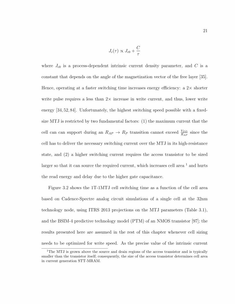
21
Jc(τ) ∝ Jc0 +C
τ
where Jc0 is a process-dependent intrinsic current density parameter, and C is a
constant that depends on the angle of the magnetization vector of the free layer [35].
Hence, operating at a faster switching time increases energy efficiency: a 2× shorter
write pulse requires a less than 2× increase in write current, and thus, lower write
energy [34, 52, 84]. Unfortunately, the highest switching speed possible with a fixed-
size MTJ is restricted by two fundamental factors: (1) the maximum current that the
cell can can support during an RAP → RP transition cannot exceed VDD
RAPsince the
cell has to deliver the necessary switching current over the MTJ in its high-resistance
state, and (2) a higher switching current requires the access transistor to be sized
larger so that it can source the required current, which increases cell area 1 and hurts
the read energy and delay due to the higher gate capacitance.
Figure 3.2 shows the 1T-1MTJ cell switching time as a function of the cell area
based on Cadence-Spectre analog circuit simulations of a single cell at the 32nm
technology node, using ITRS 2013 projections on the MTJ parameters (Table 3.1),
and the BSIM-4 predictive technology model (PTM) of an NMOS transistor [97]; the
results presented here are assumed in the rest of this chapter whenever cell sizing
needs to be optimized for write speed. As the precise value of the intrinsic current
1The MTJ is grown above the source and drain regions of the access transistor and is typicallysmaller than the transistor itself; consequently, the size of the access transistor determines cell areain current generation STT-MRAM.

22
0 1 2 3 4 5 6 7
0.0 20.0 40.0 60.0
Switching Time (ns)
Cell Size (F2)
Figure 3.2: 1T-1MTJ cell switching time as a function of cell size based on Cadence-Spectre circuit simulations at 32nm.
density Jc0 is not included in the ITRS projections, Jc0 is conservatively assumed to
be zero, which requires a 2× increase in switching current for a 2× increase in the
switching speed. If feature size is given by F , then at a switching speed of 6.7ns, a
1T-1MTJ cell occupies a 10F 2 area—a 14.6× density advantage over SRAM, which
is a 146F 2 technology [56]. As the WL
ratio of the access transistor is increased, the
current sourcing capability of the transistor improves, which reduces the switching
time to 3.1ns at a cell size of 30F 2. Increasing the size of the transistor further causes
a large voltage drop across the MTJ, which reduces the drain-source voltage of the
access transistor, pushes the device into deep triode, and ultimately limits the current
sourcing capability. As a result, the switching time reaches an asymptote at 2.6ns,
which is accomplished at a cell size of 65F 2.

23
Parameter ValueCell Size 10F 2
Switching Current 50µASwitching Time 6.7nsWrite Energy 0.3pJ/bitMTJ Resistance (RLOW/RHIGH) 2.5kΩ / 6.25kΩ
Table 3.1: STT-MRAM parameters at 32nm based on ITRS’13 projections.
3.1.2 Lookup-Table Based Computing
Field programmable gate arrays (FPGAs) adopt a versatile internal organization
that leverages SRAM to store truth tables of logic functions [91]. This not only allows
a wide variety of logic functions to be represented flexibly, but also allows FPGAs to
be re-programmed almost indefinitely, making them suitable for rapid product pro-
totyping. With technology scaling, FPGAs have gradually evolved from four-input
SRAM-based truth tables to five- and six-input tables, named lookup tables (LUT)
[20]. This evolution is due to the increasing IC integration density—when LUTs are
created with higher numbers of inputs, the area they occupy increases exponentially;
however, place-and-route becomes significantly easier due to the increased function-
ality of each LUT. The selection of LUT size is technology dependent; for example,
Xilinx Virtex-6 FPGAs use both five- and six-input LUTs, which represent the opti-
mum sizing at the 40nm technology node [91].
We propose to leverage an attractive feature of LUT-based computing other than
reconfigurability: since LUTs are constructed from memory, it is possible to im-
plement them using a leakage-resistant memory technology such as STT-MRAM to

24
reduce power. Similarly to other resistive memories, MRAM dissipates near-zero
leakage power in the data array; consequently, power density can be kept in check
by reducing the supply voltage with each new technology generation. (Typical STT-
MRAM read voltages of 0.1V are reported in the literature [34].) Due to its high
write power, the technology is best suited to implementing hardware structures that
are read-only or are seldom written. Previous work has explored the possibility of
leveraging MRAM to design L2 caches [83, 90], but this work is the first to consider
the possibility of implementing much of the combinational logic on the chip, as well as
microarchitectural structures such as register files and L1 caches, using STT-MRAM.
3.2 Fundamental Building Blocks
At a high-level, an STT-MRAM based resistive microprocessor consists of stor-
age resources such as register files, caches, and queues; functional units and other
combinational logic elements; and pipeline latches. Judicious partitioning of these
hardware structures between CMOS and STT-MRAM is critical to designing a well-
balanced system that exploits the unique area, speed, and power advantages of each
technology. Making this selection correctly requires analyzing two broad categories
of MRAM-based hardware units: those leveraging RAM arrays (queues, register files,
and caches), and those leveraging look-up tables (combinational logic and functional
units).

25
3.2.1 RAM Arrays
Large SRAM arrays are commonly organized into hierarchical structures to opti-
mize area, speed, and power tradeoffs [3]. An array comprises multiple independent
banks with separate address and data buses that can be accessed simultaneously to
improve throughput. To minimize wordline and bitline delays and to simplify decod-
ing complexity, each bank is further divided into subbanks sharing address and data
busses; unlike the case of banks, only a single subbank can be accessed at a time
(Figure 3.3). A subbank consists of multiple independent mats sharing an address
line, each of which supplies a different portion of a requested data block on every
access. Internally, each mat comprises multiple subarrays. Memory cells within each
subarray are organized as rows × columns; a decoder selects the cells connected to
the relevant wordline, whose contents are driven onto a set of bitlines to be muxed
and sensed by the column sensing circuitry. The sensed value is routed back to the
data bus of the requesting bank through a separate reply network. Different organi-
zations of a fixed-size RAM array into different numbers of banks, subbanks, mats,
and subarrays yield dramatically different area, speed, and power figures [56].
STT-MRAM and SRAM arrays share much of this high-level structure with some
important differences arising from the size of a basic cell, the loading on the bitlines
and wordlines, and the underlying sensing mechanisms. In turn, these differences
result in different leakage power, access energy, delay, and area characteristics. Since
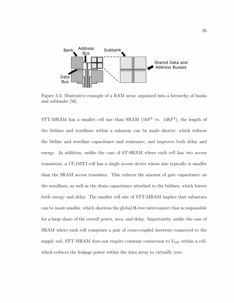
26
Bank
DataBus
AddressBus
Subbank
Shared Data and Address Busses
Figure 3.3: Illustrative example of a RAM array organized into a hierarchy of banksand subbanks [56].
STT-MRAM has a smaller cell size than SRAM (10F 2 vs. 146F 2), the length of
the bitlines and wordlines within a subarray can be made shorter, which reduces
the bitline and wordline capacitance and resistance, and improves both delay and
energy. In addition, unlike the case of 6T-SRAM where each cell has two access
transistors, a 1T-1MTJ cell has a single access device whose size typically is smaller
than the SRAM access transistor. This reduces the amount of gate capacitance on
the wordlines, as well as the drain capacitance attached to the bitlines, which lowers
both energy and delay. The smaller cell size of STT-MRAM implies that subarrays
can be made smaller, which shortens the global H-tree interconnect that is responsible
for a large share of the overall power, area, and delay. Importantly, unlike the case of
SRAM where each cell comprises a pair of cross-coupled inverters connected to the
supply rail, STT-MRAM does not require constant connection to VDD within a cell,
which reduces the leakage power within the data array to virtually zero.

27
3.2.1.1 Handling Long-Latency Writes
Despite these advantages, STT-MRAM suffers from a relatively long write la-
tency as compared to SRAM (Section 2.2.1). Leveraging STT-MRAM in designing
frequently accessed hardware structures requires (1) ensuring that critical reads are
not delayed by long-latency writes, and (2) long write latencies do not result in re-
source conflicts that hamper pipeline throughput.
One way of accomplishing both of these goals would be to choose a heavily multi-
ported organization for frequently written hardware structures. Unfortunately, this
results in an excessive number of ports, and as area and delay grow with port count,
significantly hurts performance. For example, building an STT-MRAM based ar-
chitectural register file that would support two reads and one write per cycle with
fast, 30F 2 cells at 32nm, 4GHz would require two read ports and 13 write ports2,
which would increase total port count from 3 to 15. An alternative would be to go
to a heavily multi-banked implementation without incurring the overhead of extreme
multiporting. Regrettably, as the number of banks are increased, so does the number
of H-tree wiring resources, which quickly overrides the leakage and area benefits of
using STT-MRAM.
Instead, this chapter proposes an alternative strategy that allows high write
2A write to the 30F 2 STT-MRAM cell takes 13 cycles (3.1ns×4GHz), whereas a typical SRAMbased register file accepts one write per cycle. To achieve the same write throughout as the SRAMbased register file, an STT-MRAM based register file needs 13 write ports.

28
throughput and read-write bypassing without incurring an increase in the wiring
overhead. The key idea is to allow long-latency writes to complete locally within
each subbank without unnecessarily occupying global H-tree wiring resources. To
make this possible, each subbank is augmented with a subbank buffer—an array of
flip-flops (physically distributed across all of mats within a subbank) that latch in the
data-in and address bits from the H-tree, and continue driving the subarray data and
address wires throughout the duration of a write while bank-level wiring resources are
released (Figure 3.4). In RAM arrays with separate read and write ports, subbank
buffers drive only the write port; reads from other locations within the array can
complete unobstructed, and it becomes possible to read the value being written to
the array directly from the subbank buffer.
Subbank
Shared Data and Address Busses
Subbank Buffer
Figure 3.4: Illustrative example of subbank buffers.
Subbank buffers also make it possible to perform differential writes [49], where
only bit positions that differ from their original contents are modified on a write. For
this to work, the port attached to the subbank buffer must be designed as a read-write
port; when a write is received, the subbank buffer (physically distributed across the

29
mats) latches in the new data and initiates a read for the original contents. Once
the data arrives, the original and the new contents are bitwise XOR’ed to generate
a mask indicating those bit positions that need to be changed. This mask is sent to
all of the relevant subarrays along with the actual data, and are used to enable the
bitline drivers. In this way, it becomes possible to perform differential writes without
incurring additional latency and energy on the global H-tree wiring. Differential
writes can reduce the number of bit flips, and thus the write energy, by significant
margins, and can make the STT-MRAM based implementation of heavily written
arrays practical.
3.2.1.2 Modeling STT-MRAM Arrays
To derive the latency, power, and area figures for STT-MRAM arrays, we use a
modified version of CACTI 6.5 [56] augmented with 10F 2 and 30F 2 STT-MRAM cell
models. The modifications reflect four key differences between SRAM and STT-
MRAM: (1) STT-MRAM incurs additional switching latency and energy during
writes, (2) the 1T-1R STT-MRAM cell is smaller than an SRAM cell, (3) there is no
leakage current within an STT-MRAM cell, and (4) each STT-MRAM cell has one
access transistor whereas an SRAM cell has two. The subbank buffers are modeled
as part of the the peripheral circuitry for each subbank.

30
3.2.1.3 Deciding When to Use STT-MRAM
STT-MRAM is best suited to large RAM arrays or infrequently written hardware
structures, because (1) the potential for leakage power, area, and read energy savings,
as well as read latency reduction are higher in large arrays as compared to smaller
ones, and (2) infrequently written structures require a small number of subbanks.
Deciding whether it is beneficial to implement a memory structure in STT-MRAM
requires (1) determining the minimum number of required subbanks that satisfies
the write accesses, and (2) comparing the area, leakage, energy, and latency of the
STT-MRAM and the SRAM based implementations.
A set of STT-MRAM and SRAM arrays with different sizes are evaluated in this
section. In the accompanying figures, “Best SRAM” and “Best STT-MRAM” repre-
sent the best configurations chosen by CACTI using an objective function that assigns
equal weights to delay, dynamic power, leakage power, cycle time, and area. The con-
figurations labeled as “2 Subbank STT-MRAM”, “4 Subbank STT-MRAM”, and
“8 Subbank STT-MRAM” are STT-MRAM configurations that force the respective
number of subbanks to be two, four, and eight. All of the evaluated configurations in
this section have a single port, a single bank, and a 32-bit access granularity.
Area. SRAM cells are larger STT-MRAM cells. The area of the “Best STT-MRAM”
configurations, therefore, are smaller than the area of iso-capacity “Best SRAM”

31
configurations in Figure 3.5. As the number of subbanks increases, however, an STT-
0 10 20 30 40 50 60 70 80
2KB 8KB 32KB 128KB
Area Normalized
to 2KB
SR
AM
Best SRAM
Best STT-‐MRAM
2 Subbank STT-‐MRAM
4 Subbank STT-‐MRAM
8 Subbank STT-‐MRAM
Figure 3.5: Area of different SRAM and STT-MRAM configurations.
MRAM array occupies a larger area than its SRAM-based counterpart due to the
area overhead of the subbank buffers. Hence, implementing a small and frequently
written hardware structure in STT-MRAM does not reduce area as compared to the
best SRAM implementation.
Leakage. STT-MRAM cells consume zero leakage power. As the number of subbanks
increases, the SRAM based subbank buffers and other peripheral circuits consume
greater amounts of leakage power (Figure 3.6). A small RAM structure implemented
in STT-MRAM, however, can still achieve leakage power savings: an eight subbank
2KB STT-MRAM array consumes half of the leakage power is consumed by the best
2KB SRAM configuration.

32
0
10
20
30
40
50
60
70
2KB 8KB 32KB 128KB
Leakage Po
wer
Normalized
to 2KB
SRA
M
Best SRAM
Best STT-‐MRAM
2 Subbank STT-‐MRAM
4 Subbank STT-‐MRAM
8 Subbank STT-‐MRAM
Figure 3.6: Leakage of different SRAM and STT-MRAM configurations.
Energy. A comparison of the read energy is shown in Figure 3.7. STT-MRAM
typically consumes less read energy than SRAM because of the reduced area, and the
corresponding reduction in the energy dissipated on the (shorter) wires. Write energy
is modeled as a fixed per-bit switching energy added on top of the read energy. For
large arrays, in which STT-MRAM read energy can be as low as half of the SRAM
read energy, the total write energy can also be less than that of SRAM.
0 1 2 3 4 5 6 7 8
2KB 8KB 32KB 128KB
Read
Ene
rgy Normalized
to 2KB
SRA
M
Best SRAM
Best STT-‐MRAM
2 Subbank STT-‐MRAM
4 Subbank STT-‐MRAM
8 Subbank STT-‐MRAM
Figure 3.7: Energy of different SRAM and STT-MRAM configurations.

33
Latency. STT-MRAM read latency increases as the number of subbanks increases
(Figure 3.8). In small, heavily subbanked STT-MRAM arrays, read latency is lower
than it is under the best SRAM configuration. This is because the subbank structures
increase h-tree complexity, and increase the h-tree delay.
0 0.5 1
1.5 2
2.5 3
3.5 4
2KB 8KB 32KB 128KB
Read
Laten
cy Normalized
to 2KB
SRA
M
Best SRAM
Best STT-‐MRAM
2 Subbank STT-‐MRAM
4 Subbank STT-‐MRAM
8 Subbank STT-‐MRAM
Figure 3.8: Latency of different SRAM and STT-MRAM configurations.
3.2.2 Lookup Tables
Although large STT-MRAM subarrays dissipate near-zero leakage power, the leak-
age power of the peripheral circuitry can be significant in smaller subarrays. With
smaller arrays, there are fewer opportunities to share sense amplifiers and decod-
ing circuitry across multiple rows and columns. One option to combat this problem
would be to utilize very large arrays to implement lookup tables of logic functions;
unfortunately, both the access time and the area overhead deteriorate with larger
arrays.

34
Rather than utilizing an STT-MRAM array to implement a logic function, we
rely on a specialized STT-MRAM based lookup table employing differential current-
mode logic with dynamic power management (DyCML). Prior work in this area has
resulted in fabricated, two-input lookup tables [84] at 140nm, as well as a non-volatile
full-adder prototype [52]. Figure 3.9 depicts an example three-input LUT. The circuit
needs both complementary and pure forms of each of its inputs, and the LUT produces
complementary outputs. Consequently, when multiple LUTs are cascaded in a large
circuit, there is no need to generate extra complementary outputs.
CC
AA
BB
3x8 Tree
clkclk
clk
clk
Z SAZ
clk
clk
Vdd
A
B
C
B
C
A
B
C
B
C C C C C
A
B
C
A
B
C
DEC REFDEC REF
Figure 3.9: Illustrative example of a three-input lookup table.
This LUT circuit, an expanded version of what is proposed in [84], utilizes a
dynamic current source by charging and discharging the capacitor shown in Figure 3.9.
The capacitor is discharged during the clk phase, and sinks current through the 3×8
decode tree during the clk phase. Keeper PMOS transistors charge the two entry
nodes of the sense amplifier (SA) during the clk phase and sensing is performed

35
during the clk phase. These two entry nodes, named DEC and REF, reach different
voltage values during the sensing phase (clk) since the sink paths from DEC to the
capacitor vs. from REF to the capacitor exhibit different resistances. The reference
MTJ needs to have a resistance between the low and high resistance values. Since
ITRS projects RLO and RHIGH values of 2.5kΩ and 6.25kΩ at 32nm, 4.375kΩ is
chosen for RREF .
Although the MTJ decoding circuitry is connected to VDD at the top and dynam-
ically connected to GND at the bottom, the voltage swing on the capacitor is much
smaller than VDD, which significantly reduces the access energy. The output of this
current mode logic operation is fed into a sense amplifier, which turns the low-swing
operation into a full-swing complementary output.
In [84], it is observed that the circuit can be expanded to higher numbers of in-
puts by expanding the decode tree. However, it is important to note that expanding
the tree beyond a certain height reduces noise margins and makes the LUT circuit
vulnerable to process variations, since it becomes increasingly difficult to detect the
difference between the high and low MTJ states due to the additional resistance in-
troduced by the transistors in series. As more and more transistors are added, their
cumulative resistance can become comparable to MTJ resistance, and fluctuations
among transistor resistances caused by process variations can make sensing challeng-
ing.

36
3.2.2.1 Optimal LUT Sizing for Latency, Power, and Area
Both the power and the performance of a resistive processor depend heavily on the
LUT sizes chosen to implement combinational logic blocks. This makes it necessary to
develop a detailed model to evaluate latency, area, and power tradeoffs as a function
of STT-MRAM LUT size. Figure 3.10 depicts read energy, leakage power, read delay,
and area as a function of the number of LUT inputs. LUTs with two to six inputs
(4-64 MTJs) are studied, which represent realistic LUT sizes for real circuits. As
a comparison, only five- and six-input LUTs are utilized in modern FPGAs (e.g.,
Xilinx Virtex 6) as larger LUTs do not justify the increase in latency and area for the
marginal gain in flexibility when implementing logic functions. As each LUT stores
only one bit of output, multiple LUTs are accessed in parallel with the same inputs
to produce multi-bit results (e.g., a three-bit adder that produces a four-bit output).
Read Energy. Access energy decreases slightly as LUT sizes are increased. Although
there are more internal nodes—and thus, higher gate and drain capacitances–to charge
with each access on a larger LUT, the voltage swing on the footer capacitor is lower
due to the increased series resistance charging the capacitor. As a design choice,
it is possible to size up the transistors in the decode tree to trade off power against
latency and area. The overall access energy goes down from 2fJ to 1.7fJ as LUT size is
increased from two to six for the minimum-size transistors used in these simulations.
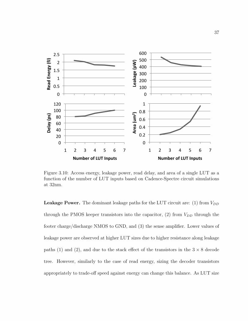
37
0
0.5
1
1.5
2
2.5 Re
ad Ene
rgy (fJ)
0 100 200 300 400 500 600
Leakage (pW)
0 20 40 60 80
100 120
1 2 3 4 5 6 7
Delay (p
s)
Number of LUT Inputs
0
0.2
0.4
0.6
0.8
1
1 2 3 4 5 6 7
Area (um
2 )
Number of LUT Inputs
Figure 3.10: Access energy, leakage power, read delay, and area of a single LUT as afunction of the number of LUT inputs based on Cadence-Spectre circuit simulationsat 32nm.
Leakage Power. The dominant leakage paths for the LUT circuit are: (1) from VDD
through the PMOS keeper transistors into the capacitor, (2) from VDD through the
footer charge/discharge NMOS to GND, and (3) the sense amplifier. Lower values of
leakage power are observed at higher LUT sizes due to higher resistance along leakage
paths (1) and (2), and due to the stack effect of the transistors in the 3 × 8 decode
tree. However, similarly to the case of read energy, sizing the decoder transistors
appropriately to trade-off speed against energy can change this balance. As LUT size

38
is increased from two to six inputs, leakage power reduces from 550pW to 400pW.
Latency. Due to the increased series resistance of the decoder’s pull-down network
with larger LUTs, the RC time constant associated with charging the footer capacitor
goes up, and latency increases from 80 to 100ps. However, LUT speed can be increased
by sizing the decoder transistors larger at the expense of a larger area, and a higher
load capacitance for the previous stage driving the LUT. For optimal results, the
footer capacitor must also be sized appropriately. A higher capacitance allows the
circuit to work with a lower voltage swing at the expense of increased area. Lower
capacitance values cause higher voltage swings on the capacitor, thereby slowing down
the reaction time of the sense amplifier due to the lower potential difference between
the DEC and REF nodes. A 50fF capacitor was used in these simulations.
Area. Although larger LUTs amortize the leakage power of the peripheral circuitry
better and offer more functionality without incurring a large latency penalty, the area
overhead of the lookup table increases exponentially with the number of inputs. Every
new input doubles the number of transistors in the branches; as LUT size is increased
from two to six inputs, the area of the LUT increases fivefold. Nevertheless, a single
LUT can replace approximately 12 CMOS standard cells on average when implement-
ing such complex combinational logic blocks as a floating-point unit (Section 3.3.5) or

39
the scheduling logic of a memory controller (Section 3.3.6.4); consequently, analyses
shown later in the chapter assume six-input LUTs unless otherwise stated.
3.2.2.2 Case Study: Three-bit Adder using Static CMOS, ROM, and
STT-MRAM LUT Circuits
To study the power and performance advantages of STT-MRAM LUT-based com-
puting on a realistic circuit, Table 3.2 compares access energy, leakage power, area,
and delay figures obtained on three different implementations of a three-bit adder: (1)
a conventional, static CMOS implementation, (2) a LUT-based implementation using
the STT-MRAM (DyCML) LUTs described in Section 3.2.2, and (3) a LUT-based
implementation using conventional, CMOS-based static ROMs. Minimum size tran-
sistors are used in all three cases to keep the comparisons fair. Circuit simulations are
performed using Cadence AMS (Spectre) with Verilog-based test vector generation;
we use 32nm BSIM-4 predictive technology models (PTM) [97] of NMOS and PMOS
transistors, and the MTJ parameters presented in Table 3.1 based on ITRS’13 pro-
jections. All results are obtained under identical input vectors, minimum transistor
sizing, and a 370K temperature. Although simulations were also performed at 16nm
and 22nm nodes, results showed similar tendencies to those presented here, and are
not repeated.

40
STT-MRAM Static ROM-BasedParameter LUT CMOS LUTDelay 100ps 110ps 190psAccess Energy 7.43fJ 11.1fJ 27.4fJLeakage Power 1.77nW 10.18nW 514nWArea 2.40µm2 0.43µm2 17.9µm2
Table 3.2: Comparison of three-bit adder implementations using STT-MRAM LUTs,static CMOS, and a static CMOS ROM. Area estimates do not include wiring over-head.
Static CMOS. A three-bit CMOS ripple-carry adder is built using one half-adder
(HAX1) and two full-adder (FAX1) circuits based on circuit topologies used in the
OSU standard cell library [80]. Static CMOS offers the smallest area among all three
designs considered because the layout is highly regular and only 70 transistors are
required instead of the 348 required for the STT-MRAM LUT-based design. Leakage
is 5.8× higher than MRAM since the CMOS implementation has a much higher
number of leakage paths than an STT-MRAM LUT, whose subthreshold leakage is
confined to its peripheral circuitry.
STT-MRAM LUTs. A three-input half-adder requires four STT-MRAM LUTs,
one for each output of the adder (three sum bits plus a carry-out bit). Since the least
significant bit of the sum depends only on two bits, it can be calculated using a two-
input LUT. Similarly, the second bit of the sum depends on a total of four bits, and
can be implemented using a four-input LUT. The most significant bit and the carry-
out bit each depend on six bits, and each of them requires a six-input LUT. Although

41
results presented here are based on unoptimized, minimum-size STT-MRAM LUTs,
it is possible to slow down the two- and four-input LUTs to save access energy by
sizing the transistors. The results presented here are conservative compared to this
best-case optimization scenario.
An STT-MRAM based three-bit adder has 1.5× lower access energy than its static
CMOS counterpart due to its energy-efficient, low-swing, differential current-mode
logic implementation; however, these energy savings are achieved at the expense of a
5.6× increase in area. In a three-bit adder, a six-input STT-MRAM LUT replaces
three CMOS standard cells. The area overhead can be expected to be lower when
implementing more complex logic functions that result in many minterms, which is
when LUT-based computation is most beneficial; for instance, a single six-input LUT
is expected to replace 12 CMOS standard cells on average when implementing the
FPU (Section 3.3.5) and the memory controller scheduling logic (Section 3.3.6.4).
The most notable advantage of the STT-MRAM LUT over static CMOS is the
5.8× reduction in leakage. This is due to the significantly smaller number of leak-
age paths that are possible with an STT-MRAM LUT, which exhibits subthreshold
leakage only through its peripheral circuitry. The speed of the STT-MRAM LUT is
similar to static CMOS: although CMOS uses higher-speed standard cells, an STT-
MRAM LUT calculates all four bits in parallel using independent LUTs.

42
CMOS ROM-Based LUTs. To perform a head-on comparison against a LUT-
based CMOS adder, we build a 64× 4 static ROM circuit that can read all three bits
of the sum and the carry-out bit with a single lookup. Compared to a 6T-SRAM
based, reconfigurable LUT used in an FPGA, a ROM-based, fixed-function LUT is
more energy efficient, since each table entry requires either a single transistor (in the
case of a logic 1) or no transistors at all (in the case of a logic 0), rather than the six
transistors required by an SRAM cell. A 6-to-64 decoder drives one of 64 wordlines,
which activates the transistors on cells representing a logic 1. A minimum sized PMOS
pull-up transistor and a skewed inverter are employed to sense the stored logic value.
Four parallel bitlines are used for the four outputs of the adder, amortizing dynamic
energy and leakage power of the decoder over the four output bits.
The ROM-based LUT dissipates 290× higher leakage than its STT-MRAM based
counterpart. This is due to two factors: (1) transistors in the decoder circuit of
the ROM represent a significant source of subthreshold leakage, whereas the STT-
MRAM LUT uses differential current-mode logic, which connects a number of access
devices in series with each MTJ on a decode tree without any direct connections
between the access devices and VDD, and (2) the ROM-based readout mechanism
suffers from significant leakage paths within the data array itself since all unselected
devices represent sneak paths for active leakage during each access. The access energy
of the ROM-based LUT is 3.7× higher than the STT-MRAM LUT, since (1) the

43
decoder has to be activated with every access, and (2) the bitlines are charged to VDD
and discharged to GND using full-swing voltages, whereas the differential current-
sensing mechanism of the STT-MRAM LUT operates with low-swing voltages.
The ROM-based LUT also runs 1.9× slower than its STT-MRAM based coun-
terpart due to the serialization of the decoder access and cell readout: the input
signal has to traverse through the decoder to activate one of the wordlines, which
then selects the transistors along that wordline. Two thirds of the delay is incurred
in the decoder. Overall, the ROM-based LUT delivers the worst results on all metrics
considered due to its inherently more complex and leakage-prone design.
3.2.2.3 Deciding When to Use LUTs
Consider a three-bit adder which has two three-bit inputs and four one-bit outputs.
This function can be implemented using four six-input LUTs, whereas the VLSI
implementation requires only three standard cells, resulting in a stdcellLUT
ratio of less
than one. On the other hand, an unsigned multiplier with two three-bit inputs and a
six-bit output requires six six-input LUTs or 36 standard cells, raising the same ratio
to six. As the size and complexity of a Boolean function increase, thereby requiring
more minterms after logic minimization, this ratio can be as high as 12 [13]. This is
due not only to the increased complexity of the function better utilizing the fixed size
of the LUTs, but also to the sheer size of the circuit allowing the boolean minimizer to

44
amortize complex functions over multiple LUTs. As this ratio gets higher, the power
consumption and leakage advantage of LUT based circuits improve dramatically. The
observation that LUT-based implementations work significantly better for large and
complex circuits is one of our guidelines for choosing which parts of a microprocessor
should be implemented using LUTs vs. conventional CMOS.
3.3 Structure and Operation of An STT-MRAM
based CMT Pipeline
Figure 3.11 shows how hardware resources are partitioned between CMOS and
STT-MRAM in an example CMT system with eight single-issue in-order cores, and
eight hardware thread contexts per core. Whether a resource can be effectively im-
plemented in STT-MRAM depends on both its size and on the expected number of
writes it incurs per cycle. STT-MRAM offers dramatically lower leakage and much
higher density than SRAM, but suffers from long write latency and high write en-
ergy. Large, wire-delay dominated RAM arrays—L1 and L2 caches, TLBs, memory
controller queues, and register files—are implemented in STT-MRAM to reduce leak-
age and interconnect power, and to improve interconnect delay. Instruction and
store buffers, PC registers, and pipeline latches are kept in CMOS due to their small
size and relatively high write activity. Since LUTs are never written at runtime,

45
PC
Logi
c
Thrd
Se
lM
ux
Inst
Bu
fx
8
Thrd
Se
lM
ux
Reg
File
x 8
Fron
t-End
Thrd
Sel
Logi
c
•I$
Mis
s•
I-TLB
Mis
s•
Inst
Buf
Ful
l•
Bran
ch
•D
$ M
iss
•D
-TLB
Mis
s•
Dep
ende
nce
•St
ruct
ure
Con
flict
CLK
CLK
CLK
CLKCLK
Cro
ssba
rIn
terfa
ce
STT-
MR
AM L
UTs
STT-
MR
AM A
rrays
Pure
CM
OS
Shar
edL2
$Ba
nks
x 8
Inst
ruct
ion
Fetc
hTh
read
Sele
ct
Dec
ode
Exec
ute
Writ
e Ba
ck
Func
Uni
tAL
U
FPU
Dec
ode
Logi
c
CLK
D$
D-T
LB
I$
I-TLB
CLK
StBu
fx
8
Mem
ory
MC
0 Q
ueue
MC
0 Log
ic
MC
1 Q
ueue
MC
1 Log
ic
MC
2 Q
ueue
MC
2 Log
ic
MC
3 Q
ueue
MC
3 Log
ic
CLK
Pre
Dec
ode
Back
-End
Thrd
Sel
Logi
c
Fig
ure
3.11
:Il
lust
rati
veex
ample
ofa
resi
stiv
eC
MT
pip
elin
e.

46
they are used to implement such complex combinational logic blocks as the front-end
thread selection, decode, and next-PC generation logic, the floating-point unit, and
the scheduling logic of the memory controller.
An important issue that affects both power and performance for caches, TLBs, and
register files is the size of a basic STT-MRAM cell used to implement the subarrays.
With 30F 2 cells, write latency can be reduced by 2.2× over 10F 2 cells (Section 2.2.1)
at the expense of lower density, higher read energy, and longer read latency. Lookup
tables are constructed from dense, 10F 2 cells as they are never written at runtime.
The register file and the L1 d-cache use 30F 2 cells with 3.1ns switching time as the
6.7ns switching time of a 10F 2 cell has a prohibitive impact on throughput. The L2
cache and the memory controller queues are implemented with 10F 2 cells and are
optimized for density and power rather than write speed; similarly, TLBs and the L1
i-cache are implemented using 10F 2 cells due to their relatively low miss rate, and
thus, low write probability.
3.3.1 Instruction Fetch
Each core’s front-end is quite typical, with a separate PC register and an eight-
deep instruction buffer per thread. The i-TLB, i-cache, next-PC generation logic,
and front-end thread selection logic are shared among all eight threads. The i-TLB
and the i-cache are built using STT-MRAM arrays; thread selection and next-PC

47
generation logic are implemented with STT-MRAM LUTs. Due to their small size
and high write activity, instruction buffers and PC registers are left in CMOS.
3.3.1.1 Program Counter Generation
Each thread has a dedicated, CMOS-based PC register. To compute the next
sequential PC with minimum power and area overhead, a special 6 × 7 “add one”
LUT is used rather than a general-purpose adder LUT. A 6 × 7 LUT accepts six
bits of the current PC plus a carry-in bit to calculate the corresponding six bits of
the next PC and a carry-out bit; internally, the circuit consists of two-, three-, four-,
five-, and six-input LUTs (one of each), each of which computes a different bit of the
seven bit output in parallel.
The overall next sequential PC computation unit comprises five such 6× 7 LUTs
arranged in a carry-select configuration (Figure 3.12). Carry out bits are used as the
select signals for a chain of CMOS-based multiplexers that choose either the new or
the original six bits of the PC. Hence, the delay of the PC generation logic is four
multiplexer delays, plus a single six-input LUT delay, which comfortably fits within
a 250ps clock period in circuit simulations (Section 3.5).
3.3.1.2 Front-End Thread Selection
Every cycle, the front-end selects one of the available threads to fetch in round-
robin order, which promotes fairness and facilitates a simple implementation. The

48
LUT-64
cout
LUT-64
cout
LUT-64
cout
LUT-64
cout
LUT-64
31 26 20 14 8 2PC
Next PC
6x7 LUT
6x7 LUT
6x7 LUT
6x7 LUT
6x7 LUT
31 26 20 14 8 2
cout cout cout cout
Figure 3.12: Next PC generation using five add-one LUTS in a carry-select configu-ration.
following conditions make a thread unselectable in the front-end: (1) an i-cache or
an i-TLB miss, (2) a full instruction buffer, or (3) a branch or jump instruction.
On an i-cache or an i-TLB miss, the thread is marked unselectable for fetch, and
is reset to a selectable state when the refill of the i-cache or the i-TLB is complete.
To facilitate front-end thread selection, the ID of the last selected thread is kept in
a three-bit CMOS register, and the next thread to fetch from is determined as the
next available, ublocked thread in round-robin order. The complete thread selection
mechanism thus requires an 11-to-3 LUT, which is built from 96 six-input LUTs
sharing a data bus with tri-state buffers—six bits of the input are sent to all of the
LUTs, and the remaining five bits are used to generate the enable signals for all
LUTs in parallel with the LUT access. (It is also possible to optimize for power by
serializing the decoding of the five bits with the LUT access, and by using the enable
signal to control the LUT clk input.)

49
3.3.1.3 L1 Instruction Cache and TLB
The i-cache and and the i-TLB are both implemented in STT-MRAM due to
their large size and relatively low write activity. Since writes are infrequent, these
resources are each organized into a single subbank to minimize the overhead of the
peripheral circuitry, and are built using 10F 2 cells that reduce area, read energy,
and read latency at the expense of longer writes. The i-cache is designed with a
dedicated read port and a dedicated write port to ensure that the front-end does
not come to a complete stall during refills; this ensures that threads can still fetch
from the read port in the shadow of an ongoing write. To accommodate multiple
outstanding misses from different threads, the i-cache is augmented with an eight-
entry refill queue. When a block returns from the L2 on an i-cache miss, it starts
writing to the cache immediately if the write port is available; otherwise, it is placed
in the refill queue while it waits for the write port to free up.
SRAM STT-MRAM STT-MRAMParameter (32KB) (32KB) (128KB)Read Delay 397ps 238ps 474psWrite Delay 397ps 6932ps 7036psRead Energy 35pJ 13pJ 50pJWrite Energy 35pJ 90pJ 127pJLeakage Power 75.7mW 6.6mW 41.4mWArea 0.31mm2 0.06mm2 0.26mm2
Table 3.3: Instruction cache parameters.
It is possible to leverage the 14.6× density advantage of STT-MRAM over SRAM

50
by either designing a similar-capacity L1 i-cache with shorter wire delays, lower read
energy, and lower area and leakage, or by designing a higher-capacity cache with
similar read latency and read energy under a similar area budget. Table 3.3 presents
latency, power, and area comparisons between a 32KB, SRAM-based i-cache; its
32KB, STT-MRAM counterpart; and a larger, 128KB STT-MRAM configuration
that fits under the same area budget 3. Simply migrating the 32KB i-cache from
SRAM to STT-MRAM reduces area by 5.2×, leakage by 11.5×, read energy by 2.7×,
and read delay by one cycle at 4GHz. Leveraging the density advantage to build
a larger, 128KB cache results in more modest savings in leakage (45%) due to the
higher overhead of the CMOS-based peripheral circuitry. Write energy increases by
2.6− 3.6× over CMOS with 32KB and 128KB STT-MRAM caches, respectively.
3.3.2 Predecode
After fetch, instructions go through a predecode stage where a set of predecode
bits for back-end thread selection are extracted and written into the CMOS-based
instruction buffer. Predecode bits indicate if the instruction is a member of the
following equivalence classes: (1) a load or a store, (2) a floating-point or integer
divide, (3) a floating-point add/sub, compare, multiply, or an integer multiply, (4) a
brach or a jump, or (5) any other ALU operations. Each flag is generated by inspecting
the six-bit opcode, which requires a total of five six-input LUTs. The subbank ID of
3The experimental setup is described in Section 3.4.

51
the destination register is also extracted and recorded in the instruction buffer during
the predecode stage to faciliate back-end thread selection.
3.3.3 Thread Select
Every cycle, the back-end thread selection unit issues an instruction from one
of the available, unblocked threads. The goal is to derive a correct and balanced
issue schedule that prevents out-of-order completion; avoids structural hazards and
conflicts on L1 d-cache and register file subbanks; maintains fairness; and delivers
high throughput.
3.3.3.1 Instruction Buffer
Each thread has a private, eight-deep instruction buffer organized as a FIFO
queue. Since buffers are small and are written every few cycles with up to four new
instructions, they are implemented in CMOS as opposed to STT-MRAM.
3.3.3.2 Back-End Thread Selection Logic
Every cycle, back-end thread selection logic issues the instruction at the head of
one of the instruction buffers to be decoded and executed. The following events make
a thread unschedulable: (1) an L1 d-cache or d-TLB miss, (2) a structural hazard
on a register file subbank, (3) a store buffer overflow, (4) a data dependency on an
ongoing long-latency floating-point, integer multiply, or integer divide instruction, (5)

52
a structural hazard on the (unpipelined) floating-point divider, and (6) the possibility
of out-of-order completion.
The buffer entry holding a load is not recycled at the time the load issues; instead,
the entry is retained until the load is known to hit in the L1 d-cache or in the store
buffer. In the case of a miss, the thread is marked as unschedulable; when the L1
d-cache refill process starts, the thread transitions to a schedulable state, and the
load is replayed from the instruction buffer. On a hit, the load’s instruction buffer
entry is recycled as soon as the load enters the writeback stage.
Long-latency floating-point instructions and integer multiplies from a single thread
can be scheduled back-to-back so long as there are no dependencies between them. In
the case of an out-of-order completion possibility—a floating-point divide followed by
any other instruction, or any floating-point instruction other than a divide followed
by an integer instruction—the offending thread is made unschedulable for as many
cycles as needed for the danger to disappear.
Threads can also become unschedulable due to structural hazards on the un-
pipelined floating-point divider, on register file subbank write ports, or on store
buffers. As the register file is built using 30F 2 STT-MRAM cells with 3.1ns switching
time, the register file subbank write occupancy is 13 cycles at 4GHz. Throughout the
duration of an on-going write, the subbank is unavailable for a new write (unless it
is the same register that is being overwritten), but the read ports remain available;

53
hence, register file reads are not stalled by long-latency writes. If the destination sub-
bank of an instruction conflicts with an ongoing write to the same bank, the thread
becomes unschedulable until the target subbank is available. If the head of the in-
struction buffer is a store and the store buffer of the thread is full, the thread becomes
unschedulable until there is an opening in the store buffer.
In order to avoid starvation, a least recently selected (LRS) policy is used to pick
among all schedulable threads. The LRS policy is implemented using CMOS gates.
3.3.4 Decode
In the decode stage, the six-bit opcode of the instruction is inspected to generate
internal control signals for the following stages of the pipeline, and the architectural
register file is accessed to read the input operands. Every decoded signal propagated
to the execution stage thus requires a six-input LUT. For a typical, five-stage MIPS
pipeline [42] with 16 output control signals, 16 six-input LUTs suffice to accomplish
this.
3.3.4.1 Register File
Every thread has 32 integer registers and 32 floating-point registers, for a total of
512 registers (2kB of storage) per core. To enable a high-performance, low-leakage,
STT-MRAM based register file that can deliver the necessary write throughput and

54
single-thread latency, integer and floating-point register from all threads are aggre-
gated in a subbanked STT-MRAM array as shown in Figure 3.13. The overall register
file consists of 32 subbanks of 16 registers each, sharing a common address bus and
a 64-bit data bus. The register file has two read ports and a write port, and the
write ports are augmented with subbank buffers to allow multiple writes to proceed
in parallel on different subbanks without adding too much area, leakage, or latency
overhead (Section 3.2.1). Mapping each thread’s integer and floating-point registers
to a common subbank would significantly degrade throughput when a single thread is
running in the system, or during periods where only a few threads are schedulable due
to L1 d-cache misses. To avert this problem, each thread’s registers are are striped
across consecutive subbanks to improve throughput and to minimize the chance of a
subbank write port conflict. Double-precision floating-point operations require read-
ing two consecutive floating-point registers starting with an even-numbered register,
which is accomplished by accessing two consecutive subbanks and driving the 64-bit
data bus in parallel.
Table 3.4 lists area, read energy, and leakage power advantages that are possible
by implementing the register file in STT-MRAM. The STT-MRAM implementation
reduces leakage by 2.4× and read energy by 1.4× over CMOS; however, energy for
a full 32-bit write is increased by 22.2×. Whether the end result turns out to be a
net power savings depends on how frequently the register file is updated, and on how

55
Shared Data and Address Busses
T0-R0 T0-R1 T0-R2 T0-R3
T0-R4 T0-R5 T0-R6 T0-R7
T1-R0 T1-R1 T1-R2 T1-R3
T1-R4 T1-R5 T1-R6 T1-R7
Figure 3.13: Illustrative example of a subbanked register file.
effective differential writes are on a given workload.
Parameter SRAM STT-MRAMRead Delay 137ps 122psWrite Delay 137ps 3231psRead Energy 0.45pJ 0.33pJWrite Energy 0.45pJ 10.0pJLeakage Power 3.71mW 1.53mWArea 0.038mm2 0.042mm2
Table 3.4: Register file parameters.
3.3.5 Execute
After decode, instructions are sent to functional units to complete their execu-
tion. Bitwise logical operations, integer addition and subtraction, and logical shifts
are handled by the integer ALU, whereas floating-point addition, multiplication, and

56
division are handled by the floating-point unit. Similar to the Sun’s Niagara-1 proces-
sor [48], integer multiply and divide operations are also sent to the FPU rather than
a dedicated integer multiplier to save area and leakage power. Although the integer
ALU is responsible for 5% of the baseline leakage power consumption, many of the
operations it supports (e.g., bitwise logical operations) do not have sufficient circuit
complexity (i.e., minterms) to amortize the peripheral circuitry in a LUT-based im-
plementation. Moreover, fully pipelining an STT-MRAM based integer adder (the
power- and area-limiting unit in a typical integer ALU [51]) requires the adder to be
pipelined in two stages, but the additional power overhead of the pipeline flip-flops
largely offsets the benefits of transitioning to STT-MRAM. Consequently, the integer
ALU is left in CMOS. The FPU, on the other hand, is responsible for a large fraction
of the per-core leakage power and dynamic access energy, and is thus implemented
with STT-MRAM LUTs.
Floating-Point Unit. To compare ASIC- and LUT-based implementations of the
floating-point unit, an industrial FPU design from Gaisler Research, the GRFPU [13],
is taken as a baseline. A VHDL implementation of the GRFPU synthesizes to 100,000
gates on an ASIC design flow, and runs at 250MHz at 130nm; on a Xilinx Virtex-
2 FPGA, the unit synthesizes to 8,500 LUTs, and runs at 65MHz. Floating-point

57
addition, subtraction, and multiplication are fully pipelined and execute with a three-
cycle latency; floating-point division is unpipelined and takes 16 cycles.
To estimate the required pipeline depth for an STT-MRAM LUT-based imple-
mentation of the GRFPU to operate at 4GHz at 32nm, we use published numbers
on configurable logic block (CLB) delays on a Virtex-2 FPGA [2]. A CLB has a
LUT+MUX delay of 630ps and an interconnect delay of 1 to 2ns based on its place-
ment, which corresponds to a critical path of six to ten CLB delays. For STT-
MRAM, we assume a critical path delay of eight LUTs, which represents the average
of these two extremes. Assuming a buffered six-input STT-MRAM LUT delay of
130ps and a flip-flop sequencing overhead (tsetup + tC→Q) of 50ps, and conservatively
assuming a perfectly-balanced pipeline for the baseline GRFPU, we estimate that
the STT-MRAM implementation would need to be pipelined eight times deeper than
the original to operate at 4GHz, with floating-point addition, subtraction, and mul-
tiplication latencies of 24 cycles, and an unpipelined, 64-cycle floating-point divide
latency. When calculating leakage power, area, and access energy, we account for the
overhead of the increased number of flip-flops due to this deeper pipeline (flip-flop
power, area, and speed are extracted from 32nm circuit simulations of the topology
used in the OSU standard cell library [80]). We characterize and account for the
impact of loading on an STT-MRAM LUT when driving another LUT stage or a
flip-flop via Cadence-Spectre circuit simulations.

58
To estimate the pipeline depth for the CMOS implementation of the GRFPU run-
ning at 4GHz, we first scale the baseline 250MHz frequency linearly from 130nm to
32nm, which corresponds to a frequency of 1GHz at 32nm. Thus, conservatively ig-
noring the sequencing overhead, to operate at 4GHz, the circuit needs to be pipelined
4× deeper, with 12-cycle floating-point addition, subtraction, and multiplication la-
tencies, and a 64-cycle, unpipelined floating-point division. Estimating power for
CMOS (100,000 gates) requires estimating dynamic and leakage power for an av-
erage gate in a standard-cell library. We characterize the following OSU standard
cells using circuit simulations at 32nm, and use their average to estimate power for
the CMOS-based GRFPU design: INVX2, NAND2X1, NAND3X1, BUFX2, BUFX4,
AOI22X1, MUX2X1, DFFPOSX1, and XNORX1.
Table 3.5 shows the estimated leakage, dynamic energy, and area of the GRFPU
in both pure CMOS and STT-MRAM. The CMOS implementation uses 100, 000
gates whereas the STT-MRAM implementation uses 8,500 LUTs. Although each
CMOS gate has lower dynamic energy than a six-input LUT, each LUT can replace
12 logic gates on average. This 12× reduction in unit count results in an overall
reduction of the total dynamic energy. Similarly, although each LUT has higher
leakage than a CMOS gate, the cumulative leakage of 8,500 LUTs reduces leakage
by 4× over the combined leakage of 100, 000 gates. Area, on the other hand, is
comparable due to the reduced unit count compensating for the 5× higher area of

59
each LUT and the additional buffering required to cascade the LUTs. (Note that
these area estimates do not account for wiring overheads in either the CMOS or the
STT-MRAM implementations.) In summary, the FPU is a good candidate to place
in STT-MRAM since its high circuit complexity produces logic functions with many
minterms that require many CMOS gates to implement, which is exactly when a
LUT-based implementation is advantageous.
Parameter CMOS FPU STT-MRAM FPUDynamic Energy 36pJ 26.7pJLeakage Power 259mW 61mWArea 0.22mm2 0.20mm2
Table 3.5: FPU parameters. Area estimates do not include wiring overhead.
3.3.6 Memory
In the memory stage, load and store instructions access the STT-MRAM based
L1 d-cache and d-TLB. To simplify the scheduling of stores and to minimize the
performance impact of contention on subbank write ports, each thread is allocated a
CMOS-based, eight-deep store buffer holding in-flight store instructions.
3.3.6.1 Store Buffers
One problem that comes up when scheduling stores is the possibility of a d-cache
subbank conflict at the time the store reaches the memory stage. Since stores require
address computation before their target d-cache subbank is known, thread selection

60
logic cannot determine if a store will experience a port conflict in advance. To address
this problem, the memory stage of the pipeline includes a CMOS-based, private,
eight-deep store buffer per thread. So long as a thread’s store buffer is not full,
the thread selection logic can schedule the store without knowing the destination
subbank. Stores are dispatched into and issued from store buffers in FIFO order; store
buffers also provide an associative search port to support store-to-load forwarding,
similar to the Sun Niagara-1 processor [48]. We assume relaxed consistency models
where special synchronization primitives (e.g., memory fences in weak consistency, or
acquire/release operations in release consistency) are inserted into store buffers, and
the store buffer enforces the semantics of the primitives when retiring stores and when
forwarding to loads. Since the L1 d-cache supports a single write port (but multiple
subbank buffers), only a single store can issue per cycle. Store buffers, and the L1
refill queue contend for access to this shared resource, and priority is determined
based on a round-robin policy.
3.3.6.2 L1 Data Cache and TLB
Both the L1 d-cache and the d-TLB are implemented using STT-MRAM arrays.
The d-cache is equipped with two read ports (one for snooping, and one for the
core) and a write port shared among all subbanks. At the time a load issues, the
corresponding thread is marked unschedulable and recycling of the instruction buffer

61
entry holding the load is postponed until it is ascertained that the load will not
experience a d-cache miss. Loads search the store buffer of the corresponding thread
and access the L1 d-cache in parallel, and forward from the store buffer in the case
of a hit. On a d-cache miss, the thread is marked unschedulable, and is transitioned
back to a schedulable state once the data arrives. To accommodate refills returning
from the L2, the L1 has a 16-deep, CMOS-based refill queue holding incoming data
blocks. Store buffers and the refill queue contend for access to the two subbanks
of the L1, and are given access using a round-robin policy. Since the L1 is written
frequently, it is optimized for write throughput using 30F 2 cells. The L1 subbank
buffers perform internal differential writes to reduce write energy.
SRAM STT-MRAM STT-MRAMParameter (32KB) (32KB, 30F 2) (64KB, 30F 2)Read Delay 344ps 236ps 369psWrite Delay 344ps 3331ps 3399psRead Energy 60pJ 31pJ 53pJWrite Energy 60pJ 109pJ 131pJLeakage Power 78.4mW 11.0mW 31.3mWArea 0.54mm2 0.19mm2 0.39mm2
Table 3.6: L1 d-cache parameters.
Table 3.6 compares the power, area, and latency characteristics of two different
STT-MRAM based L1 configurations to a baseline, 32KB CMOS implementation. A
capacity-equivalent, 32KB d-cache reduces the access latency from two clock cycles to
one, and cuts down the read energy by 1.9× due to the shorter interconnect lengths
possible with the density advantage of STT-MRAM. Leakage power is reduced by

62
7.1×, and area is reduced by 2.8×. An alternative, 64kB configuration requires 72%
of the area of the CMOS baseline, but increases capacity by 2×; this configuration
takes two cycles to read, and delivers a 2.5× leakage reduction over CMOS.
3.3.6.3 L2 Cache
The L2 cache is designed using 10F 2 STT-MRAM cells to optimize for density
and access energy rather than write speed. To ensure adequate throughput, the cache
is equipped with eight banks, each of which supports four subbanks, for a total of 32.
Each L2 bank has a single read/write port shared among all of the subbanks; unlike
the L1 d-cache and the register file, L2 subbanks are not equipped with differential
writing circuitry to minimize leakage due to the CMOS-based periphery.
Table 3.7 compares two different STT-MRAM L2 organizations to a baseline,
4MB CMOS L2. To optimize for leakage, the baseline CMOS L2 cache uses high-Vt
transistors in the data array, whereas the peripheral circuitry needs to be imple-
mented using low-Vt, high-performance transistors to maintain a 4GHz cycle time.
A capacity-equivalent, 4MB STT-MRAM based L2 reduces leakage by 2.0× and read
access energy by 63% compared to a CMOS baseline. Alternatively, it is possible to
increase capacity to 32MB while maintaining lower area, but the leakage overhead of
the peripheral circuitry increases with capacity, and results in twice as much leakage
as the baseline.

63
SRAM STT-MRAM STT-MRAMParameter (4MB) (4MB) (32MB)Read Delay 2364ps 1956ps 2760psWrite Delay 2364ps 7752ps 8387psRead Energy 1268pJ 798pJ 1322pJWrite Energy 1268pJ 952pJ 1477pJLeakage Power 6578mW 3343mW 12489mWArea 82.33mm2 32.00mm2 70.45mm2
Table 3.7: L2 cache parameters.
3.3.6.4 Memory Controllers
To provide adequate memory bandwidth to eight cores, the system is equipped
with four DDR2-800 memory controllers. Memory controller read and write queues
are implemented in STT-MRAM using 10F 2 cells. Since the controller needs to make
decisions every DRAM clock cycle (10 processor cycles in our baseline), the impact
of write latency on scheduling efficiency and performance is negligible.
The scheduling logic of the controller is implemented using STT-MRAM LUTs.
To estimate power, performance, and area under CMOS- and MRAM-based imple-
mentations, we use a methodology similar to that employed for the floating-point
unit. We use a DDR2-800 memory controller IP core developed by HiTech [32] as
our baseline; on an ASIC design flow, the controller synthesizes to 13, 700 gates and
runs at 400MHz; on a Xilinx Virtex-5 FPGA, the same controller synthesizes to 920
CLBs and runs at 333MHz. Replacing CLB delays with STT-MRAM LUT delays,
we find that an STT-MRAM based implementation of the controller would meet the

64
400MHz cycle time without further modifications.
Table 3.8 compares the parameters of the CMOS and STT-MRAM based imple-
mentations. Similarly to the case of the FPU, the controller logic benefits significantly
from a LUT based design. Leakage power is reduced by 7.2×, while the energy of
writing to the scheduling queue increases by 24.4×.
Parameter CMOS STT-MRAMRead Delay 185ps 154psWrite Delay 185ps 6830psRead Energy 7.1pJ 5.6pJWrite Energy 7.1pJ 173pJMC Logic Energy 30.0pJ 1.6pJLeakage Power 41.4mW 5.72mWArea 0.097mm2 0.051mm2
Table 3.8: Memory controller parameters. Area estimates do not include the wiringoverhead.
3.3.7 Write Back
In the write-back stage, an instruction writes its result back into the architectural
register file through the write port. No conflicts are possible during this stage since the
thread selection logic schedules instructions by taking register file subbank conflicts
into account. Differential writes within the register file reduce write power during
write backs.

65
3.4 Experimental Setup
This section presents the experimental methodology used for the evaluation. Architecture-
level simulations are conducted to model the behavior of the proposed system. Circuit-
level tools and simulators are used to evaluate the area, latency, and power. A set of
13 parallel benchmarks are evaluated on the proposed STT-MRAM based systems.
3.4.1 Architecture
We use a heavily modified version of the SESC simulator [65] to model a Niagara-
like in-order CMT system with eight cores, and eight hardware thread contexts per
core. Table 3.9 lists the microarchitectural configuration of the baseline cores and the
shared memory subsystem.
For STT-MRAM, we experiment with two different design points for the L1 and
L2 caches: (1) configurations with capacity equivalent to the CMOS baseline, where
STT-MRAM benefits from the lower interconnect delays (Table 3.10-Small), and (2)
configurations with a larger capacity that still fit within same area budget as the
CMOS baseline, where STT-MRAM benefits from fewer misses (Table 3.10-Large).
The STT-MRAM memory controller queue write delay is set to 27 processor cycles.
We experiment with an MRAM-based register file with 32 subbanks and a write delay
of 13 cycles each, and we also evaluate the possibility of leaving the register file in
CMOS.

66
Processor ParametersFrequency 4 GHz
Number of cores 8Number of SMT contexts 8 per core
Front-end thread select Round RobinBack-end thread select Least Recently Selected
Pipeline organization Single-issure, in-orderStore buffer entries 8 per thread
L1 CachesiL1/dL1 size 32kB/32kB
iL1/dL1 block size 32B/32BiL1/dL1 round-trip latency 2/2 cycles(uncontended)
iL1/dL1 ports 1 / 2iL1/dL1 banks 1 / 2
iL1/dL1 MSHR entries 16/16iL1/dL1 associativity direct mapped/2-way
Coherence protocol MESIConsistency model Release consistency
Shared L2 Cache and Main MemoryShared L2 cache 4MB, 64B block, 8-way
L2 MSHR entries 64L2 round-trip latency 10 cycles (uncontended)
Write buffer 64 entriesDRAM subsystem DDR2-800 SDRAM [53]
Memory controllers 4
Table 3.9: Parameters of baseline.
Small LargeiL1/dL1 size 32kB/32kB 128kB/64kBiL1/dL1 latency 1/1 cycles 2/2 cyclesL1s write occupancy 13 cycles 13 cyclesL2 size 4MB 32MBL2 latency 8 cycles 12 cyclesL2 write occupancy 24 cycles 23 cycles
Table 3.10: STT-MRAM cache parameters
67
For structures that reside in CMOS in both the baseline and the proposed archi-
tecture (e.g., pipeline latches, store buffers), McPAT [50] is used to estimate power,
area, and latency.
3.4.2 Circuit
We use BSIM-4 predictive technology models (PTM) of NMOS and PMOS tran-
sistors at 32nm, and perform circuit simulations using Cadence AMS (Spectre) mixed
signal analyses with Verilog-based input test vectors. Only high performance transis-
tors were used in all of the circuit simulations. Temperature is set to 370K in all cases,
which is a meaningful thermal design point for the proposed processor operating at
4GHz [58].
3.4.3 Applications
A set of 13 parallel benchmarks are evaluated (Table 3.11). These include three
applications from NU-MineBench [60], two from a openMP implementation of the
NAS parallel benchmarks [7], two from SPEC OMP2001 [4], and six from SPLASH-
2 [89].
3.5 Evaluation
This section presents the evaluations on performance and power.

68
Benchmark Description Problem size
Data MiningBLAST Protein matching 12.3k sequencesBSOM Self-organizing map 2,048 rec., 100 epochs
KMEANS K-means clustering 18k pts., 18 attributes
NAS OpenMPMG Multigrid Solver Class ACG Conjugate Gradient Class A
SPEC OpenMPSWIM Shallow water model MinneSpec-Large
EQUAKE Earthquake model MinneSpec-Large
Splash-2 KernelsCHOLESKY Cholesky factorization tk29.O
FFT Fast Fourier transform 1M pointsLU Dense matrix division 512× 512to16× 16
RADIX Integer radix sort 2M integers
Splash-2 ApplicationsOCEAN Ocean movements 514×514 ocean
WATER-N Water-Nsquared 512 molecules
Table 3.11: Simulated applications and their input sizes.
3.5.1 Performance
Figure 3.14 compares the performance of four different MRAM-based CMT con-
figurations to the CMOS baseline. When the register file is placed in STT-MRAM
and the L1 and L2 cache capacities are made equivalent to CMOS, performance de-
grades by 11%. Moving the register file to CMOS improves performance, at which
point the system achieves 93% of the baseline performance. Enlarging both L1 and
L2 cache capacities under the same area budget reduces miss rates but loses the la-
tency advantage of the smaller caches; this configuration outperforms CMOS by 2%

69
0
0.2
0.4
0.6
0.8 1
1.2
BLAST
BSOM
CG
CHOLESKY
EQUAKE
FFT
KMEA
NS
LU
MG
OCEAN
RADIX
SWIM
WATER
-‐N G
EOMEA
N
Performance Normalized to CMOS
CMOS
Small L1&
L2, STT-‐M
RAM RF
Small L1&
L2, CMOS RF
Large L1&L2, CMOS RF
Small L1, Large L2, CMOS RF
Fig
ure
3.14
:P
erfo
rman
ce.
0.0
5.0
10.0
15.0
20.0
BLAST
BSOM
CG
CHOLESKY
EQUAKE
FFT
KMEA
NS
LU
MG
OCEAN
RADIX
SWIM
WATER
-‐N
AVER
AGE
Total Power (W)
CMOS
Small L1&
L2, STT-‐M
RAM RF
Small L1&
L2, CMOS RF
Large L1&L2, CMOS RF
Small L1, Large L2, CMOS RF
Fig
ure
3.15
:T
otal
Pow
er.

70
on average. Optimizing the L2 for fewer misses (by increasing capacity under the
same area budget) while optimizing the L1s for fast hits (by migrating to a denser
STT-MRAM cache with same capacity) delivers similar results.
In general, performance bottlenecks are application dependent. For applications
such as CG, FFT and WATER, the MRAM-based register file represents the biggest
performance hurdle. These applications encounter a higher number of subbank con-
flicts than others, and when the register file is moved to CMOS, their performance
improves significantly. EQUAKE, KMEANS, MG, and RADIX are found sensitive
to floating-point instruction latencies as they encounter many stalls due to depen-
dents of long-latency floating-point instructions in the 24-cycle, STT-MRAM based
floating-point pipeline. CG, CHOLESKY, FFT, RADIX, and SWIM benefit most
from increasing the cache capacities under the same area budget as CMOS by lever-
aging the density advantage of STT-MRAM.
3.5.2 Power
Figure 3.15 compares total power dissipation across the five systems. STT-MRAM
configurations that maintain the same cache sizes as CMOS reduce the total power by
1.7× over CMOS. Despite their higher performance potential, configurations which
increase cache capacity under the same area budget increase power by 1.2× over
CMOS, due to the significant amount of leakage power dissipated in the CMOS-based

71
11.40
5.32 5.34
14.92 14.48
0
2
4
6
8
10
12
14
CMOS Small L1 and L2, STT-‐MRAM
RF
Small L1 and L2, CMOS RF
Large L1 and L2, CMOS RF
Small L1, Large L2, CMOS RF
Leakage Po
wer (W
)
RF
FPU
ALU and Bypass
InstBuf and STQ
FFs and Comb Logic
L1s and TLBs
L2
MC
Figure 3.16: Leakage Power.

72
decoding and sensing circuitry in the 32MB L2 cache. Although a larger L2 can reduce
the write power by allowing for fewer L2 refills and writes to the memory controllers’
scheduling queues, the increased leakage power consumed by the peripheral circuitry
outweighs the savings on dynamic power.
Figure 3.16 shows the breakdown of leakage power among different components
for the evaluated systems. Total leakage power is reduced by 2.1× over CMOS when
the cache capacities are kept the same. Systems with a large L2 cache increase leakage
power by 1.3× due to the CMOS-based periphery. The floating-point units, which
consume 18% of the total leakage power in the CMOS baseline, benefit significantly
from an STT-MRAM based implementation. STT-MRAM based L1 caches and TLBs
together reduce leakage power by another 10%. The leakage power of the memory
controllers in STT-MRAM is negligible, whereas in CMOS it is 1.5% of the total
leakage power.
3.6 Summary
This chapter presents a new technique that reduces leakage and dynamic power in
a deep-submicron microprocessor by migrating power- and performance-critical hard-
ware resources from CMOS to STT-MRAM. We have evaluated the power and per-
formance impact of implementing on-chip caches, register files, memory controllers,
floating-point units, and various combinational logic blocks using magnetoresistive

73
circuits, and we have explored the critical issues that affect whether a RAM array or
a combinational logic block can be effectively implemented in MRAM. We have ob-
served significant gains in power-efficiency by partitioning on-chip hardware resources
among STT-MRAM and CMOS judiciously to exploit the unique power, area, and
speed benefits of each technology, and by carefully re-architecting the pipeline to
mitigate the performance impact of long write latencies and high write power.

74
Chapter 4
STT-MRAM based Main
Memories
DRAM density scaling is jeopardized by two fundamental charge retention prob-
lems in deeply scaled technology nodes: (1) the reduced storage capacitance of the
DRAM cell makes it difficult to store large amounts of charge, and (2) the stored
charge is lost faster due to increased leakage through the access transistor. Emerging
non-volatile memory (NVM) technologies aim at skirting the charge retention problem
of deeply scaled DRAM by relying on resistance—rather than electrical charge—to
represent information. However, each of the candidate NVMs comes with its own set
of shortcomings: phase change memory (PCM) and resistive random access memory

75
(RRAM) exhibit limited write endurance and high switching energy, while STT-
MRAM density lags multiple generations behind that of current generation DRAM.
One important reason for the lower density of STT-MRAM compared to DRAM
is the access transistor, which must be sufficiently large to supply the write current
required to switch the device. Note that in Chapter 3, STT-MRAM density exhibit
higher density compared to SRAM even when a larger access transistor is used to
supply a high write current. In fact, for embedded STT-MRAM discussed in Chap-
ter 3, the density of STT-MRAM is limited by the strict design rules. For stand-alone
STT-MRAM, aggressively reducing the dimensions of the storage element over suc-
cessive technology generations can reduce the required write current, removing one
of the major impediments to rapid capacity scaling1. Reducing the size, however,
inevitably results in a lower thermal stability and a higher probability of retention
errors, which necessitate a combination of multi-bit error correcting code (ECC) and
periodic scrubbing techniques [21,57].
Scrubbing operations are expensive, each of which requires (1) reading out a code-
word spanning one or more memory blocks before the number of accumulated errors
exceeds the correction capability of the underlying ECC mechanism, (2) checking and
correcting any errors, and (3) writing back the corrected data. Employing a stronger
ECC can help tolerate more errors before a scrub operation becomes mandatory,
1Other impediments include the conventional challenges of technology scaling, such as processvariability and yield.

76
0.01$
0.1$
1$
10$
0$ 2$ 4$ 6$ 8$ 10$ 12$ 14$ 16$
Scrubb
ing)Freq
uency)(Hz))
ECC)Granularity)(Number)of)64B)Blocks))
Higher ScrubbingOverhead
More ExpensiveECC Checks
Figure 4.1: Tradeoff between scrubbing frequency and ECC granularity under a 12.5%storage overhead.
thereby reducing the scrubbing frequency and the concomitant performance and en-
ergy overheads. For a given ECC storage overhead, the ECC strength can be improved
by coarsening the ECC granularity (i.e., increasing the size of a codeword) and in-
creasing the number of errors that can be corrected in each codeword [12]. Figure 4.1
shows that coarsening the ECC granularity from one to sixteen blocks while main-
taining a fixed storage overhead reduces the required scrubbing frequency by more
than 200× (the calculation of the curve in Figure 4.1 is described in Section 4.1.3).
However, large codewords increase the access energy and bandwidth usage due to
over-fetching. Specifically, when a codeword spans multiple cache blocks, (1) a read
requires fetching multiple blocks to decode the ECC, and (2) a write requires reading
the entire codeword and updating the check bits.
We introduce Sanitizer—a low-cost, energy-efficient memory system architecture

77
that protects high-capacity, STT-MRAM based main memories against retention er-
rors. To avoid fetching multiple blocks from memory and performing costly ECC
checks on every read, memory regions (contiguous, 4KB sections of the physical ad-
dress space) that will be accessed in the near future are predicted and proactively
scrubbed. The key insight is that when accessing a recently scrubbed block, it is
sufficient to perform a lightweight ECC check. By anticipating the memory regions
that will be accessed in the near future and scrubbing them in advance, Sanitizer
improves performance by 1.22× and reduces end-to-end system energy by 22% over
a baseline STT-MRAM system at 22 nm.
4.1 Background for Sanitizer
Before taking an in-depth look at Sanitizer, it is instructive to review DRAM
error protection techniques, STT-MRAM fault modeling, and known techniques for
protecting STT-MRAM against retention errors.
4.1.1 DRAM Error Protection
With technology scaling, maintaining DRAM reliability has become increasingly
challenging. To address the problem, solutions that span novel devices, circuits,
architectures, and software have been devised.

78
4.1.1.1 Error Correcting Codes
The reliability of a memory system can be improved with the help of ECC, which
adds redundant bits to a group of data bits to form a codeword. For a specified ECC
configuration, the smallest Hamming distance between any pair of valid codewords
is called the minimum distance of the ECC; any number of errors fewer than the
minimum distance changes a valid codeword into an invalid one. For example, the
single error correction double error detection (SECDED) Hamming code has a min-
imum distance of four. On a single bit error, the original data can be restored by
finding the valid codeword closest to the invalid bit pattern. Errors due to two bit
flips can be detected but not corrected by SECDED ECC, because an erroneous bit
pattern with two errors can have the same minimum Hamming distance to multiple
valid codewords.
Protection against STT-MRAM retention errors necessitates an ECC with multi-
bit error correction capability [21,57]. BCH [10,33] and Reed Solomon codes [64] are
two widely used ECC schemes for multi-bit error correction. Sanitizer builds upon
a binary BCH code because the symbol-based Reed Solomon code is optimized for
correcting bursts of errors, which are not a common retention failure pattern in STT-
MRAM [21,57]. A binary BCH code with k data bits, capable of t-bit error correction
and (t+ 1)-bit error detection, requires r redundant bits to form an n-bit codeword,
in which n = k + r and r = t×dlog2(n+ 1)e+ 1.

79
Sanitizer employs a hierarchical error protection mechanism comprising local and
global ECCs. The local ECC protects a single data block, while the global ECC
encodes data that spans multiple blocks. Prior work in using hierarchical ECC to
protect main memory aims at reducing the over-fetching cost of chipkill [22]. Yoon et
al. [94] propose a virtualized, multi-tier ECC architecture that decouples the physical
mapping of the data and its associated ECC. Udipi et al. [86] propose a hierarchical
ECC, which separates error detection from correction by storing the checksum and
parity bits in each memory chip. Unlike prior work, which activates the first and
second level ECCs in sequence, Sanitizer leverages knowledge of whether a memory
location has been scrubbed recently to determine if it is safe to rely on a fast, local
ECC check.
4.1.1.2 Refresh and Scrub Operations
A DRAM cell can retain sufficient charge for a limited amount of time (typically
64 ms) after it is written; consequently, cells must be refreshed periodically to protect
against information loss. Unlike DRAM, STT-MRAM does not have a charge leakage
problem. However, it suffers from retention errors due to thermal fluctuations that
may abruptly and randomly change the contents of the memory cells. Hence, unlike
the case of DRAM retention errors where charge is gradually removed from the cells,

80
STT-MRAM retention errors cannot be prevented using refresh. This trait neces-
sitates using error correcting codes in conjunction with scrubbing in STT-MRAM
systems [57].
A memory system protected by ECC can tolerate a fixed number of errors per
codeword. No matter how strong the underlying ECC is, however, after a sufficiently
long period of time, the number of errors that accumulate in a block can exceed
the correction capability of the ECC, thereby resulting in an uncorrectable error.
Scrubbing is a standard strategy to meet this challenge, in which a memory block is
periodically read, checked for errors, and restored to an error-free state.
4.1.2 STT-MRAM Reliability
Errors in STT-MRAM can occur during both the read and the write operations.
A read error occurs when the resistance range of the high and low states overlap
due to process variability [57, 72]. Advanced sensing schemes [18, 85] and reference
resistance tuning [85] can reduce the read errors. A write error occurs when either the
amplitude of the write current is not sufficiently high, or its duration is not sufficiently
long. Reducing the MTJ diameter and thickness can reduce the critical current
IC0 and the thermal stability factor ∆, which lowers the amplitude of the required
write current [75]. If the required write current is sufficiently low, a minimum-size
transistor can reliably and quickly switch the state of the MTJ. Repeated writes can

81
also lead to hard errors. However, the endurance of STT-MRAM is a less pressing
issue compared to other non-volatile memory technologies such as RRAM or PCM.
Nevertheless, if the endurance of STT-MRAM were to become a concern, techniques
proposed for PCM [38,62] could be adopted to alleviate the problem. Such techniques
are orthogonal to Sanitizer, and are beyond the scope of the problem to be solved in
this chapter.
Current generation STT-MRAM exhibits low density due to the large access tran-
sistor required to supply a sufficiently high switching current. Industry projections
indicate, however, that technology scaling will effectively address this problem; for
instance, a recent paper [73] from Everspin shows that the saturation current of a
minimum-sized transistor will be higher than the required switching current below
28nm. As technology scales, the MTJ size has to be shrunk as well, which inevitably
results in an increase in the retention error rate. The best known technology [28, 45]
at 22nm already exhibits a high retention error rate due to low thermal stability.
These retention errors are projected to be the dominant type of error in deeply scaled
STT-MRAM [57]. The retention error rate can be calculated using a closed form
analytical expression:
Pretention(∆, t) = 1− exp(− t
τ0
exp(−∆)), ∆ =
EbkBT
(4.1)
where t is the time elapsed since the last write, τ0 is a process-dependent constant

82
(typically 1ns), Eb is the temperature-independent activation energy, kB is the Boltz-
mann constant, and T is the absolute temperature in Kelvins [57]. As technology
scales, ∆ is predicted to decrease since IC0 must be reduced to allow reliable write
operations with lower current [21]. A perpendicular MTJ, in which the magnetiza-
tion direction of the fixed and free layers are both orthogonal to the tunneling barrier,
achieves a lower IC0 with a higher ∆ compared to a conventional in-plane MTJ [28];
however, even for a perpendicular MTJ, the ∆ at 20 nm is in the range of 29 to
34 [28,45], which is lower than the required ∆ (>60 [57]) for a 1GB memory without
ECC. Note that these are the ∆ values measured at room temperature; ∆ further
decreases at higher temperatures.
Due to process variations, ∆ is not uniform across all of the cells on a single chip.
Specifically, if ∆ follows a distribution characterized by a probability mass function
f(∆), the probability that a random cell has a retention error at time t is:
P (t) = Σ∆max∆min
Pretention(∆, t)f(∆). (4.2)
This calculation is performed when computing the raw bit error rate (BER) used in
the rest of this chapter.
Naeimi et al. [57] and Del Bel et al. [21] propose to use ECC and scrubbing to
protect STT-MRAM based caches against retention errors. They restrict the ECC
granularity to one cache line. Protecting STT-MRAM based main memory against

83
retention errors poses a greater challenge than protecting caches, because (1) it takes
longer to scrub a high capacity main memory system, and (2) scrubbing contends with
demand misses for the limited off-chip memory bandwidth. Awasthi et al. [5] propose
the light array read for PCM resistance drift detection (LARDD) technique, which
places simple ECC logic on the memory chips to detect the first sign of a PCM resis-
tance drift. This scheme would not work for STT-MRAM retention errors, because
the occurrence of one STT-MRAM retention error does not change the probability of
the next one (Equation (4.1)), whereas the observation of one PCM resistance drift
error increases the likelihood of subsequent drift errors.
4.1.3 Reliability Target
The failure in time (FIT) is a standard industrial metric to measure the reliability
of a device (e.g., a DRAM die [54]). FIT measures the number of failures in one
billion device hours. We use 1 FIT (uncorrectable errors in one billion device hours)
per Gbit as a reliability target, so that if the hard failure rate of STT-MRAM is
similar to that of DRAM (22 to 33 FIT [74, 76, 77]), the retention failures have a
minimum impact on system reliability. To achieve this 1 FIT reliability target, an
appropriate ECC code must be chosen for a desired scrubbing frequency. For a given
scrubbing frequency, the raw BER can be calculated from equations (4.1) and (4.2),
and an ECC code is chosen so that the failure probability is below 1 FIT. For a specific

84
ECC code that can correct t errors and detect t+ 1 errors, the failure probability of
a single ECC codeword is Pcodeword =(nt+1
)pt+1(1 − p)n−t−1, where n is the number
of bits in a codeword. The failures due to retention errors in each codeword and the
length of the scrubbing interval can be assumed independent from each other because
(1) all of the correctable errors are corrected after each scrubbing operation, (2) all of
the detectable but uncorrectable errors are handled by higher-level mechanisms (e.g.,
roll back in a system that supports checkpointing), and (3) the probability of having
an undetectable error typically is orders of magnitude lower as compared to that of
having a detectable error. The number of failures in one billion data bits and one
billion hours, therefore, follows a binomial distribution, and the expected number of
failures caused by retention errors is Fretention = Pcodeword × Ncodeword × Nscrub FIT,
where Ncodeword is the number of codewords that cover one billion data bits, and Nscrub
is the number of scrub operations to each memory location in one billion hours.
4.1.4 Scrubbing Overheads
The performance penalty due to scrubbing increases in proportion to the capacitybandwidth
ratio of the memory system. Using a stronger ECC mitigates the bandwidth over-
head. Table 4.1 shows the off-chip memory bandwidth consumed by scrubbing under
progressively stronger ECC configurations, normalized to the peak memory band-
width of the system. (Note that the 1- and 2-block configurations are not practical

85
System Capacity / 4-blk 8-blk 16-blkconfigurations bandwidth ECC ECC ECCEvaluated (Section 4.3) 2.16 GB/GBps 9.89% 4.41% 2.73%SPARC M5 [59] 2.50 GB/GBps 11.64% 5.23% 3.23%Xeon E7-8800 [37] 2.56 GB/GBps 11.99% 5.35% 3.31%Power S822 [36] 2.67 GB/GBps 12.70% 5.48% 3.45%
Table 4.1: Bandwidth overhead due to scrubbing. FIT/Gbit<1, ∆=34, T=45C, rawBER=3.4×10⁻⁵/s and block size=64B.
because the bandwidth overhead is greater than 50%.) The scrubbing rates of all of
the configurations in Table 4.1 are below 0.05 Hz, which is much lower than the typi-
cal DRAM refresh rates ( 164 ms
= 15.6 Hz). However, scrubbing an STT-MRAM page
is more expensive than refreshing a DRAM page because scrubbing requires reading
the data out of the memory system. A sensitivity analysis on the capacitybandwidth
ratio is
presented in Section 4.4.4.2.
4.2 Sanitizer Architecture
Sanitizer reduces the scrubbing frequency by applying BCH codes with strong er-
ror tolerance to long codewords spanning multiple cache blocks. Figure 4.2 illustrates
the operation of three different memory protection techniques: (a) frequent scrubbing
combined with a fast but weak ECC, (b) infrequent scrubbing combined with a strong
but slow ECC, and (c) Sanitizer. All three techniques perform scrubbing to remove
errors from blocks B0 and B1. Since the strong ECC can correct more errors than
the fast ECC, it allows more errors to accumulate in a codeword before scrubbing

86
B0Re
ad B
0Re
ad B
1
(a) F
requ
ent s
crub
bing
with
f
ast b
ut w
eak
ECC
(b) I
nfre
quen
t scr
ubbi
ng w
ith
str
ong
but s
low
EC
C
(c) S
aniti
zer
Tim
e
Tim
e
Tim
e
B0B1
B1B1
B0B0 B0
B1
B0B1
B0B1
B0 B0B1B1
B0B1
B0B1
Scru
b Re
adRe
ques
t Rea
dEC
C C
odew
ord
Read
Fig
ure
4.2:
Illu
stra
tive
exam
ple
ofSan
itiz
eran
dco
nve
nti
onal
scru
bbin
gm
echan
ism
s.

87
becomes mandatory. As a result, the strong ECC requires scrubbing less frequently
than the fast ECC. However, the strong ECC has to be applied to longer codewords
spanning two cache blocks to achieve the same storage overhead as the fast ECC,
which requires reading an extra cache block with every memory access. As shown
in Figure 4.2 (b), both B0 and B1 must be accessed to perform error correction on
every read. Sanitizer addresses this problem using (1) a hierarchical error protection
mechanism, in which the strong ECC is used for infrequent scrubbing, while the fast
ECC is used for most of the ordinary memory accesses; and (2) a novel prediction
mechanism for scheduling scrub operations at the granularity of 4KB memory regions
prior to ordinary accesses, reducing the error correction cost.
Sanitizer relies on the observation that a recently scrubbed memory block tends
to accumulate relatively few errors and can be protected using a simple ECC. It uses
a global ECC (GECC) for scrubbing, and a local ECC (LECC) for detecting up to
three errors per memory block. When the LECC is applied within a short period of
time after a codeword is scrubbed, it can ensure the same FIT as the GECC. If an
error is detected by the LECC, the GECC mechanism is invoked for correction.
Figure 4.3 shows the Sanitizer datapath. For every read request, the system first
checks a recently scrubbed table (RST) 1 . On an RST hit, the memory block can
be accessed via LECC decoding; on a miss, multiple cache blocks must be read to
perform GECC decoding. Prior to decoding, the requests are enqueued in a request

88
RequestQueue
ScrubQueue
Arbiter
Data Buffer
GECC Cache
CommandsTo Memory
EvictFill
FromMemory
Per Channel
RecentlyScrubbed
Table
DataTo LLC
ScrubGenerator
Global and LocalECC Logic
Shared Among All Channels
RequestsFrom LLC 1
2
3 5
4
6 7
8
9
Figure 4.3: An illustration of the proposed Sanitizer architecture.
queue 2 . A DDR3 controller services the memory requests, and after receiving the
corresponding data from memory, the controller uses either the LECC or the GECC
decoder for error correction 3 .
Every write requires updating both the LECC and the GECC bits. To reduce
the number of updates to the GECC, Sanitizer employs a GECC cache that stores a
limited number of recently updated GECC bits. On every write, the RST is searched
first 1 . A hit in the RST indicates that the write request can benefit from a fast
block access via LECC; therefore, the old data block is read from main memory via
a read request 2 . Next, the GECC cache is searched for the relevant GECC bits 4 .

89
If the GECC is found in the cache, it is overwritten with the new GECC bits 5 ;
otherwise, the old GECC bits are retrieved from main memory, updated, and placed
in the GECC cache. The GECC cache implements a write-back policy to write the
updated GECC bits to main memory 7 .
Sanitizer determines the memory locations to be scrubbed based on an epoch-
based runtime algorithm. A scrubbing epoch is a window of time whose precise du-
ration is computed as region sizechannel capacity×scrubbing frequency
, which ranges from 2 µs to 10 µs.
Sanitizer determines the minimum scrubbing rate based on the ECC strength and the
error rate. The number of RST hits and misses during the current epoch are tracked
in separate counters. At the beginning of each scrubbing epoch, a scrub generator
consults these counters to determine the new memory regions to be scrubbed 8 .
4.2.1 Scheduling Scrub Operations
Unlike DRAM refresh, a scrub operation can be decomposed into accesses to
global codewords that can be scheduled through fine-grained DDR3 commands.2 On
the one hand, this creates new opportunities for more efficient command scheduling;
on the other hand, it necessitates a complex command scheduler. Sanitizer alleviates
this complexity by decoupling scrub scheduling from DDR3 command scheduling. As
shown in Figure 4.3, every scrub operation is scheduled from a scrub queue. The
requests in the scrub queue are either issued by a scrub generator, or are evicted from
2Due to the large recovery time in DRAM, ultra fine-grained refresh is not beneficial [8].

90
the global ECC cache. Figure 4.4 depicts an entry of the scrub queue, comprising
(1) a valid bit that indicates the scrub transaction is in progress, (2) a ready flag
indicating that the next required DDR3 command can be issued to memory without
violating any DDR3 timing constraints, (3) the number of remaining reads required to
complete fetching the global codeword, (4) the number of remaining writes required
to finish updating the global codeword, (5) a current operation flag indicating the
next command to be issued to main memory, (6) an actual operation flag that shows
the access type of the original request, and (7) address bits pointing to the global
codeword in main memory.
ready # reads # writes current op actual op addressvalid
Figure 4.4: An illustrative example of a scrub queue entry.
Using these flags, every scrub operation completes the following steps before leav-
ing the scrub queue: (1) fetch all of the required data blocks from memory and place
them in a data buffer; (2) send a check request to the ECC hardware and wait until
the ECC check is complete; and (3) if the check fails, correct and update the codeword
using global ECC.
As shown in Figure 4.3, an arbiter selects the DDR3 commands from the request
and scrub queues. When scheduling the scrub operations, the arbiter implements a
scheduling policy similar to the defer-until-empty (DUE) policy [82], which was orig-
inally proposed for lowering DRAM refresh overheads. By default, memory requests

91
are prioritized over scrub operations unless the number of deferred scrub operations
exceeds a threshold. 3 When the threshold is reached, scrub operations are prioritized
over memory requests until the scrub queue is empty. Sanitizer allows data forward-
ing from a recently scrubbed block in the data buffer to read requests in the request
queue.
The key to designing an efficient, fine-grained scrub scheduler is to issue scrub
requests to the memory controller at a rate slightly above the minimum scrubbing
frequency, thereby allowing sufficient slack for the controller to schedule scrub accesses
to maximize performance. For example, decreasing the duration of the scrubbing in-
terval by 2× makes it safe to schedule an individual scrub operation at any time
within the interval. However, a highly overprovisioned scrubbing rate hurts both
performance and energy. The solution that Sanitizer adopts is to incorporate a san-
itizer scrubber on top of a patrol scrubber with a slightly increased scrubbing rate:
the patrol scrubber linearly scans the physical address space to ensure that all of
the memory locations are scrubbed before a scrubbing deadline is violated; the sani-
tizer scrubber, as a result, can freely schedule extra scrub operations to any memory
location to improve performance.
3The threshold is set to half of the queue size, and the scrub frequency is sufficiently overprovi-sioned to ensure that no timing violations can occur due to postponed scrub operations.

92
4.2.2 Reducing the Read Overhead
Reducing the read overhead requires scheduling scrub operations in a timely fash-
ion so that most of the ordinary requests hit in the RST, and hence can be handled
using the local ECC.
4.2.2.1 Local ECC
Sanitizer employs a two-level hierarchical ECC. A codeword comprising multiple
blocks is protected by a strong, BCH based global ECC. In addition, each data block
is protected by a fast, local ECC. For a specified error rate, a stronger local ECC
can prolong the expiration time of a block—the time after which memory accesses
can no longer avoid using the global ECC. The expiration time is set to minimize
the probability that the number of errors in a cache block exceeds the protection
capability of the local ECC (probability < 10−15). (When calculating the system
FIT rate, we take into account both the local and the global ECC failures.) In order
to increase the local ECC protection strength with an acceptable storage overhead,
Sanitizer leverages the SECDED code, which can be configured either to correct one
error and detect two, or to detect three errors and correct none. Sanitizer is based
on the latter configuration. The local ECC adds an extra storage overhead of 11 bits
to a 64B cache block.

93
4.2.2.2 Recently Scrubbed Table
The RST is used to record memory regions that can be checked using the lo-
cal ECC. Memory locations the recently have been scrubbed by the in-order patrol
scrubber do not need to be added to the RST. Instead, two address comparators are
sufficient to delineate the boundaries of the regions which the patrol scrubber has re-
cently visited. Memory locations that are scrubbed out-of-order need to be recorded
in the RST. To keep the hardware overhead low, each entry of the RST represents a
4KB memory region. The RST is implemented as a set-associative cache to strike a
balance between performance and energy. (A sensitivity study on the RST param-
eters is presented in Section 4.4.4.3.) As shown in Figure 4.5, every RST entry has
a region identifier (RID), a counter (Cnt) recording the number of hits to the corre-
sponding region within the current epoch, and a time stamp (Time) that records the
expiration time.4
Every RST entry has to expire after a fixed expiration time (in the range of
10 − 50ms), which is determined by the thermal stability factor, the local ECC
strength, and the reliability target. A circular counter generates a time stamp for
each new region added to the RST. For example, when region D is added (Figure 4.5),
a counter value of six is recorded as its time stamp. The counter is incremented by
one at the end of every scrubbing epoch, and is reset to zero when it reaches the
4Each entry also has a valid bit and a scrubbing direction bit, which are omitted in the figure forsimplicity.

94
Add D
(a) Add a region
A 6 0RID Cnt Time
B 3 1C 10 5
Add E, F
(b) Evict two regions and add two new ones
A 5 0RID Cnt Time
B 2 1C 4 5D 11 6
0
RID Cnt Time
E 0 7F 0 7D 0 6
Add Nothing
(c) Expire a region
A 4 0RID Cnt Time
E 9 7F 2 7D 8 6
6
A 0 0RID Cnt Time
B 0 1C 0 5D 0 6
7
A 0 0RID Cnt Time
E 0 7F 0 7D 0 6
6
CircularCounter
7
0
CircularCounter
CircularCounter
CircularCounter
CircularCounter
CircularCounter
Figure 4.5: An illustrative example of the operations in a four-entry RST with anexpiration time of seven.
expiration time. All of the entries whose time stamps match the counter are evicted,
after which any new entires are added. In Figure 4.5 (c), region A is evicted because
its time stamp matches the counter.
The recently scrubbed regions might not all fit in the RST. If a particular set of
the RST is full, the entry with the lowest hit count is evicted, which is accomplished
by comparing all of the counters in the same set using comparators organized in a
tree topology. All of the hit counters are reset to zeroes at the beginning of each

95
scrubbing epoch to adapt to application phase behavior.
4.2.2.3 Scrub Generator
At the end of each scrubbing epoch, the scrub generator decides which memory
regions to scrub next. For the patrol scrubber, the region ID is incremented by one to
generate the next region. For the sanitizer scrubber, a missed region table (MRT) is
used to record the misses in the RST. The regions to be scrubbed next are determined
by inspecting the MRT and the RST at the end of a scrubbing epoch (Figure 4.6).
The MRT estimates the regions with frequent RST misses using a sticky sam-
pling algorithm. Every entry in the MRT represents a contiguous 4KB region of the
physical address space, and comprises (1) the address of the last read or write to the
represented region, (2) a valid bit indicating that the entry is in use, (3) an access
counter recording the number of accesses to the region, (4) a sticky counter used
to avoid evicting the entry before it collects sufficient statistics, and (5) a direction
counter to predict the scrubbing direction. On an MRT access, if the accessed region
already exists in the MRT, the access counter of that region is incremented by one;
otherwise, a new entry is added with the sticky counter set to all ones. All of the
non-zero sticky counters are decremented by one every time the MRT is accessed.
When the MRT is full, the following steps are required to decide whether a new entry
can be inserted: (1) a pseudo-random number R is generated by a linear-feedback

96
A 5 fwdRID Cnt Direction
B 2 bwdC 4 fwdD 11 fwd
Scrub Generator Recently Scrubbed Table
To be scrubbed:
RID Cnt DirectionG 3 6F 7 12
MissedRegionTable
F fwdE fwd
G bwd
Figure 4.6: An illustrative example of generating a maximum of three scrubbingregions using a direction threshold equals to eight.
shift register (LFSR), and (2) R is compared to the access counter of the least fre-
quently accessed non-sticky5 entry; if R is greater than or equal to the value of the
access counter, the entry is replaced by the new one. The MRT tracks whether the
accesses to a given region are in ascending or descending order using the direction
counter, which is a saturating up/down counter. On every access to a valid MRT
entry, the previous address stored in the entry is compared to the new address. If the
new address is greater than the previous one, the direction counter is incremented;
otherwise, the counter is decremented.
At the end of every epoch, the scrub generator needs to accomplish two tasks: (1)
to determine the maximum number of regions to be scrubbed for the next epoch, and
(2) to select the memory regions to be scrubbed by inspecting the MRT and the RST.
We observed that the maximum number of regions to be scrubbed in each epoch is a
5An MRT entry becomes non-sticky when its sticky counter equals zero.

97
parameter critical to performance. If too many regions are scrubbed within a fixed-
length epoch, the scrubbing overhead becomes too high and significantly degrades
performance. However, scrubbing too few regions in an epoch results in higher RST
miss rates, and ultimately a greater number of cases where the expensive global ECC
rather than the cheaper, local ECC must be used. The scrub generator determines
the maximum number of regions to be scrubbed based on the RST miss rate during
each scrubbing epoch. Two counters in the RST track the total number accesses
and the total number of misses. At the end of each epoch, the counters are used to
compute the miss rate. The maximum number of regions to be scrubbed during the
next epoch is determined by comparing the miss rate to four predefined thresholds.
Adapting the scrubbing rate to the RST miss rate allows a high scrubbing rate at the
beginning of a burst of memory accesses, and a low scrubbing rate when most of the
memory regions recently have been scrubbed.
The scrub generator prioritizes the MRT entries over RST entries when selecting
the memory regions to be scrubbed. This is because the miss region has a higher
prediction accuracy. The following rules are followed when selecting a memory region:
(1) no duplicates are allowed in the RST, and (2) the number of newly generated
regions is not allowed to exceed an upper bound.
The scrub generator uses the region ID of the most frequently accessed MRT
entry to scrub in the next epoch. When this region is scrubbed, its region ID and a

98
direction flag (computed based on the direction counter) are recorded in the RST.6
To select a region based on the RST, the scrub generator computes a new region
ID according to the current region ID and the direction flag of the most frequently
accessed entry. If the flag indicates a forward direction, the closest ascending region is
selected; otherwise, the closest descending region is scrubbed. As shown in Figure 4.6,
region D in the RST is frequently accessed during the current epoch; therefore, the
scrub generator selects one of its neighboring regions (i.e., C or E) to be scrubbed in
the next epoch. In this example, due to the forward scrubbing flag of D, region E is
selected for scrubbing.
4.2.3 Reducing the Write Overhead
In a memory system protected by large BCH codewords, a write generates more
traffic than a read. On every write, an entire local codeword, as well as the global
ECC bits, need to be updated. These updates require generating new local and global
ECC bits for the corresponding blocks. Therefore, all of the data blocks that are part
of the same global codeword must be present at the memory controller before a write
can complete, which creates extra memory traffic and degrades the overall bandwidth
efficiency. Sanitizer significantly reduces these overheads by (1) eliminating the need
for fetching the entire global codeword by generating differential global ECCs, (2)
6The scrubbing flag is set to backward if the scrubbing direction counter is below a predefinedthreshold; otherwise, it is set to forward.

99
adopting a careful data layout that allows for parallel access to global ECC bits, and
(3) eliminating most of the read accesses by caching global ECCs at the memory
controller.
4.2.3.1 Global ECC Cache
Writes are optimized by caching the global ECC bits. Our experiments show that
92% of the writes are to previously updated global codewords. Sanitizer exploits
this phenomenon by adding a 256-entry, 16-way set associative SRAM cache to each
memory channel. Every cache entry contains a valid bit, tag bits, global ECC bits,
and flag bits for implementing the least recently used (LRU) replacement policy.
4.2.3.2 Global ECC Update
Figure 4.7 shows an example application of Sanitizer to a conventional nine-chip
DIMM.7 A global codeword comprising four data blocks A, B, C, and D is stored
in memory. A block is spread across the nine chips; it consists of a local codeword
(comprising 512 data bits and 11 local ECC bits), and a part of the global ECC bits.
Using a single block access, the memory controller can read or update an entire local
codeword; however, accessing a global codeword requires multiple reads and writes.
To update the global codeword, all of the four blocks (i.e., A, B, C, and D)
must be read from memory. Then, a new GECC is written to memory via multiple
7All of the chips are ×8 and transfer the data in bursts of eight beats.

100
...A0B0
D0
C0
Chip 0A5B5
ECCD
C5
Chip 5A6B6
D5
ECCC
Chip 6ECCA
B7
D7
C7
Chip 8A7
ECCB
D6
C6
Chip 7A4B4
D4
C4
Chip 4
Block[4] Block[5] Block[6] Block[7] Block[8]Block[0] ...
Chip 4 Chip 5 Chip 6 Chip 7 Chip 8Chip 0 ...
(a) Chip Organization
(b) Data Selection
Figure 4.7: An illustrative example of the proposed memory layout for a four-blockcodeword.
accesses. Sanitizer eliminates the block reads by performing a differential update to
global codewords. For instance, a write to block A requires the following steps: (1)
the old contents of A are retrieved from the memory by a read access, (2) a differential
global codeword is formed by computing the bitwise XOR between the old and new
contents of A, (3) a parity matrix is used to generate the differential ECC bits used
for updating the global ECC, (4) the old global ECC bits are read from the memory,
(5) the new global ECC bits are generated by XORing the differential ECC and the
old global ECC bits, (6) the new value of A and the updated local ECC are written
back to the memory in one write access, and (7) the newly generated global ECC bits
are written to the GECC cache.

101
When a global ECC is evicted from the GECC cache, Sanitizer performs a fast
update to the global ECC bits in main memory by leveraging an optimized data
layout. As shown in Figure 4.7 (a), parts of each block are shifted to ensure that the
ECC bits of a global codeword are spread across the chips. (For example, B7 is shifted
right by one chip and ECCB is stored in chip 7.) Moreover, every chip supports a
base and offset addressing mode, where the base is the block address and the offset
is either zero or the chip ID. A simplified crossbar at the memory controller ensures
the right order of bits for both the local and the global codewords (Figure 4.7 (b)).
4.2.4 Support for Chipkill ECC
The goal of chipkill-level error protection is to recover the data from a failed
chip. In addition to pin failures, chipkill can protect against a burst of errors due to
wordline, bitline, or interconnect wire failures. As explained in Section 4.1.1, multi-
bit symbol codes [15, 64] are optimized for bursty errors. For example, a commercial
chipkill ECC [86] can protect against the failure of a ×4 chip by adding four check
symbols to 32 data symbols, where each symbol consists of four bits, the block size
is 128B, and the burst length is eight. When both random and bursty errors are
prevalent, two ECCs can be concatenated: one code (e.g., BCH) protects against
random errors; the other code (e.g., a symbol code) protects against bursty errors.
An example of combining Sanitizer with a single-symbol correction double-symbol

102
detection (SSCDSD) ECC [15, 86] is shown in Figure 4.8. For each group of 128
Blockn
Block1
Data01 GECC01 Chipkill
Data02 GECC02 Chipkill
Data07 GECC07 Chipkill
Block0
4x4 bits4x32 bits
Figure 4.8: Illustrative example of supporting chipkill ECC.
data bits, a subset of the Sanitizer GECC bits (BCH ECC) are appended to the
data bits, and the SSCDSD ECC bits are computed by treating the BCH ECC bits
as data. For example, Data01 and GECC01 are together protected by four four-bit
redundant symbols against chip failures. Note that a four-check SSCDSD code with
four-bit symbols can protect codewords up to 256 symbols [15]. The local ECC of
Sanitizer can be replaced by the chipkill ECC because the correction capability of
the SSCDSD code is strictly greater than that of the SECDED code. The failure
rates due to bursty errors reported in field studies range from 22 to 33 FIT per
chip [74,76,77]. Assuming a 27.5 FIT chip failure rate, the SSCDSD code can reduce
the failure rate of a DRAM system by a factor of 1.2×10⁷. Table 4.2 reports the

103
patrol scrubbing rates for an STT-MRAM system with both the SSCDSD code and
Sanitizer, configured to achieve the same failure rate as a DRAM system protected
only by the SSCDSD code. The configuration of 18.75% storage overhead adds three
2 Blocks 4 Blocks 8 Blocks18.75% Storage Overhead 0.095 Hz 0.048 Hz 0.027 Hz
25% Storage Overhead 0.026 Hz 0.014 Hz 0.010 Hz
Table 4.2: Required patrol scrubbing rates for combining Sanitizer with chipkill.
×4 ECC chips to every 16 data chips to hold both Sanitizer and the chipkill ECC;
in contrast, the 25% storage overhead setting adds four chips to every 16 chips. The
storage overhead for chipkill ECC is fixed at 12.5% for all of the configurations. Note
that the 1-block configurations do not need the ECC hierarchy in Sanitizer; however
their high scrubbing rates result in significant system performance overheads.
4.3 Experimental Setup
This section presents the experimental methodology used to evaluate Sanitizer.
Architecture-level simulations are conducted to model the behavior of the proposed
system. Circuit-level tools and simulators are used to evaluate the area, latency, and
power overheads of Sanitizer. We evaluate a Sanitizer-enabled system with twenty-
two applications.
104
4.3.1 Architecture
We use the SESC simulator [65] to model a 4GHz, eight-core out-of-order pro-
cessor. A 144GB main memory comprising DDR3-2133 compatible STT-MRAM
modules is evaluated. Detailed architecture-level parameters are listed in Table 4.3.
Notably, the precharge time (tRP) has a value lower than the corresponding DRAM
timing constraint since STT-MRAM does not precharge the bitlines during the precharge
operation. The write recovery time (tWR) is higher than the DRAM timing due to
the additional switching latency required by the STT-MRAM cells.
We use McPAT [50] to evaluate the area and power of individual components
of the processor. We use Cacti-3DD [17] to simulate the area, power, and access
latency of STT-MRAM based main memory and the storage structures associated
with Sanitizer, including the global ECC cache, the scrub queue, the recently scrubbed
table, and the missed region table (Section 4.2). Logic and memories are modeled
based on 22nm technology using parameters from ITRS 2013 [39]. STT-MRAM
specific parameters are listed in Table 4.4.
We consider various ECC codeword length that maintain approximately the same
ECC storage overhead (all under 12.5%). Table 4.5 shows the ECC capability and
the associated storage overheads for each coding scheme. The numbers in the top row
indicate the number of cache blocks that are considered part of a single codeword. For
instance, in base-2, two cache blocks—a total of 1024 bits—are guarded by a global

105
Processor Parameters
Technology 22nmFrequency 4.0 GHz
Number of cores 8Fetch/issue/commit width 4/4/4
Int/FP/LdSt/Br units 2/2/1/2Int/FP Multiplier 1/1
Int/FP IssueQ entries 32/32loadQ/storeQ/ROB entries 24/24/96
Int/FP registers 96/96Branch predictor Hybrid
Local/global/meta tables 2K/2K/8KBTB/RAS entries 4K/32
IL1 cache (private) 32KB, direct-mapped, 64B block1-cycle hit time
DL1 cache (private) 32KB, 4-way, LRU, 64B block2-cycle hit time
Cache coherence MESI protocolL2 cache (shared) 8MB, 8-way, LRU, 64B block
16-cycle hit time
Memory Controller Parameters
Address mapping page interleavingScheduling policy FR-FCFS
Request queue 64 entriesScrub queue 32 entries
Recently scrubbed table 8-way, 16K entriesMissed region table 64 entries
GECC cache 16-way, 256-entries
DDR3-2133 STT-MRAM memory system - 144 GB total capacity
Technology 22nmFrequency 1066 MHz
Chip capacity 16 GbNumber of chips per rank 9
Number of ranks per channel 2Number of channels 4
Row buffer size 8 KBTiming tRCD: 14, tCL: 14, tRP: 1, tRAS: 36, tRC: 37
(memory cycles) tBURST: 4, tCCD: 4, tWTR: 8, tWR: 22tRTP: 8, tRRD: 6, tFAW: 27
Table 4.3: System architecture and core parameters.
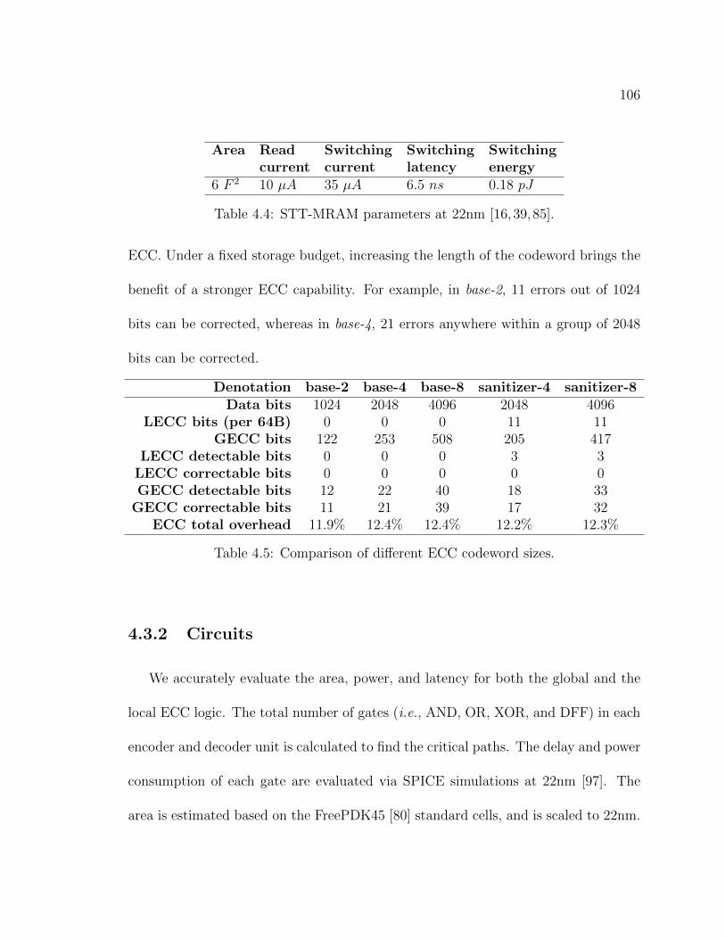
106
Area Read Switching Switching Switchingcurrent current latency energy
6 F 2 10 µA 35 µA 6.5 ns 0.18 pJ
Table 4.4: STT-MRAM parameters at 22nm [16,39,85].
ECC. Under a fixed storage budget, increasing the length of the codeword brings the
benefit of a stronger ECC capability. For example, in base-2, 11 errors out of 1024
bits can be corrected, whereas in base-4, 21 errors anywhere within a group of 2048
bits can be corrected.
Denotation base-2 base-4 base-8 sanitizer-4 sanitizer-8Data bits 1024 2048 4096 2048 4096
LECC bits (per 64B) 0 0 0 11 11GECC bits 122 253 508 205 417
LECC detectable bits 0 0 0 3 3LECC correctable bits 0 0 0 0 0GECC detectable bits 12 22 40 18 33
GECC correctable bits 11 21 39 17 32ECC total overhead 11.9% 12.4% 12.4% 12.2% 12.3%
Table 4.5: Comparison of different ECC codeword sizes.
4.3.2 Circuits
We accurately evaluate the area, power, and latency for both the global and the
local ECC logic. The total number of gates (i.e., AND, OR, XOR, and DFF) in each
encoder and decoder unit is calculated to find the critical paths. The delay and power
consumption of each gate are evaluated via SPICE simulations at 22nm [97]. The
area is estimated based on the FreePDK45 [80] standard cells, and is scaled to 22nm.

107
To meet system throughput requirements, a parallel implementation with multiple
XOR trees (similar to [41]) is used to generate the local and global ECC check bits.
The design of the local and global BCH decoders is similar to prior work [81]. The
decoding process comprises three major steps [9]: (1) syndrome generation, which
reuses the XOR-tree architecture from BCH encoding; (2) finding an error-location
polynomial, which implements an iterative algorithm proposed by Strukov [81]; and
(3) finding error-location numbers using a serial implementation that alleviates the
area and power costs.
4.3.3 Applications
We evaluate a set of 22 benchmarks comprising six parallel applications from
SPLASH-2 [89] and SPEC OMP2001 [4], as well as 16 serial applications from SPEC2006 [79].
The parallel applications are simulated to completion. To reduce the execution time
of the serial applications, we use SimPoint [31] and determine a representative 100
million instruction region from each SPEC 2006 application.
4.4 Evaluation
We first evaluate the performance, energy, and area of Sanitizer. Next, we present
sensitivity studies, compare an STT-MRAM based main memory equipped with San-
itizer to a conventional DRAM system, and evaluate how Sanitizer stacks up against

108
a baseline STT-MRAM system that combines scrubbing with hierarchical ECC and
prefetching.
4.4.1 Performance
We study the performance of three baseline configurations and three Sanitizer
systems. Figure 4.10 compares the performance of the evaluated Sanitizer systems to
the best baseline configuration (base-4 ). Due to the additional read traffic for a GECC
check on every memory access, increasing the size of the GECC codeword results
in a performance degradation for the baseline systems. This performance penalty
effectively nullifies the benefits of using longer codewords to lower the scrubbing
rate. Consequently, base-4 outperforms base-8 and base-16 (Figure 4.9). Sanitizer
mitigates the undue data traffic by using the LECC on most of the memory accesses
(85% of the time, on average). The sanitizer-4, sanitizer-8, and sanitizer-16 systems
achieve, respectively, average speedups of 1.11×, 1.22×, and 1.14× over base-4. The
corresponding scrubbing rates are 0.098 Hz, 0.043 Hz, and 0.027 Hz.
0
0.5
1
1.5
baseline read opt only
read opt & GECC$
sani8zer
Performan
ce
Normalized
to
base-‐4
4 blocks 8 blocks 16 blocks
Figure 4.9: Performance improvement analysis.

109
0 0.5 1
1.5 2
2.5
art ch
olesk
y eq
uake
fft
ocea
n sw
im
astar
bz
ip2 gc
c go
bmk
libqu
antu
m mc
f omne
tpp
sjeng
xa
lancb
mk
dealI
I lbm
mi
lc na
md po
vray
sople
x sphin
x3 ge
omea
n
Speedup Over the Baseline (base-‐4)
saniDzer-‐4
saniDzer-‐8
saniDzer-‐16
Fig
ure
4.10
:Syst
emp
erfo
rman
ceco
mpar
ison
.
0
0.5 1
1.5
art ch
olesk
y equa
ke
fft oc
ean
swim
as
tar
bzip2
gc
c go
bmk
libqu
antu
m mc
f omne
tpp
sjeng
xa
lancb
mk
dealI
I lbm
mi
lc na
md po
vray
sople
x sp
hinx ge
omea
n
Energy Normalized to the Baseline (base-‐4)
saniCzer-‐4
saniCzer-‐8
saniCzer-‐16
Fig
ure
4.11
:Syst
emen
ergy
com
par
ison
.

110
Figure 4.9 shows a breakdown of the performance improvements. The bars labeled
as “read opt only” represent the improvements achieved after adding the RST and
the MRT to reduce the read overheads (Section 4.2.2). The bars labeled as “read
opt & GECC$” represent the results of adding the GECC cache (Section 4.2.3.1)
on top of the RST and the MRT. Implementing the layout optimizations discussed
in Section 4.2.3.2 in addition to the read optimizations and the GECC cache gives
the full benefit of Sanitizer. The four-block configuration of read opt only exhibits
a small performance loss compared to baseline because Sanitizer requires a higher
scrubbing frequency. Read opt & GECC$ achieves average write traffic reductions
between 1.13-1.88× over read opt only.
4.4.2 Energy and Power
Figure 4.11 shows the end-to-end system energy. The baseline systems suffer from
two sources of energy inefficiency: (1) frequent scrubbing operations, and (2) exces-
sive memory traffic due to over-fetching. By addressing the over-fetching problem,
Sanitizer achieves lower energy consumption as compared to the most energy-efficient
baseline (base-4 ). Sanitizer-4, sanitizer-8, and sanitizer-16 respectively reduce the
system energy down to 93%, 78%, and 88% of base-4. This energy reduction is due to
two effects: (1) Sanitizer significantly reduces the data movement on memory reads
and writes, which results in lower energy; and (2) Sanitizer accelerates the execution

111
of the applications, which results in leakage energy savings. The energy breakdown
of the sanitizer-8 system is shown in Table 4.6.
Cores and Memory Main Buses and Sanitizercaches controller memory interfaces hardware63.7% 7.4% 18.3% 7.9% 2.7%
Table 4.6: Sanitizer-8 system energy breakdown.
Table 4.7 shows the peak dynamic power and the leakage power of Sanitizer.
The Sanitizer hardware consumes a peak power of 539.7 mW. The average power of
Sanitizer represents less than 3% of the total system power. The global and local
ECC hardware together consistute the major contributor to the power consumption
of Sanitizer (2.2% of the total system power); this is because of the high-performance
design choices that were made to achieve the required throughput.
ECC Scrub RST GECC Scrub Total(mW ) Logic Generator Cache Queue
Dynamic 280.5 18.1 77.6 28.8 5.9 410.9Leakage 98.8 0.9 12.3 14.3 2.5 128.8
Table 4.7: Peak dynamic power and leakage of Sanitizer components (eight blockconfiguration).
4.4.3 Area
The total area of the Sanitizer hardware corresponds to less than 1% of the pro-
cessor die area. Table 4.8 shows a breakdown of the area occupied by various system
components.

112
ECC Scrub RST GECC Scrub Total(mm2) Logic Generator Cache QueueArea 0.41 0.002 0.12 0.12 0.004 0.66
Table 4.8: Area breakdown of the Sanitizer components.
4.4.4 Sensitivity Analysis
We study the sensitivity of Sanitizer to the raw bit error rate (BER), the memory
capacitybandwidth
ratio, and the RST parameters.
4.4.4.1 Raw BER
The raw BER has a profound effect on the required scrubbing frequency. Either a
Temperature(C) ∆=37 ∆=36 ∆=35 ∆=3445 2.5×10⁻⁶ 6.0×10⁻⁶ 1.4×10⁻⁵ 3.4×10⁻⁵
55 6.7×10⁻⁶ 1.6×10⁻⁵ 3.6×10⁻⁵ 8.4×10⁻⁵
65 1.7×10⁻⁵ 3.8×10⁻⁵ 8.7×10⁻⁵ 2.0×10⁻⁴
75 4.1×10⁻⁵ 9.0×10⁻⁵ 2.0×10⁻⁴ 4.4×10⁻⁴
85 9.3×10⁻⁵ 2.0×10⁻⁴ 4.4×10⁻⁴ 9.5×10⁻⁴
Table 4.9: Raw Retention BER per second. (5% variation on ∆.)
low thermal stability factor (∆) or a high temperature can result in a high retention
BER and a high scrubbing overhead (Section 4.1.2). The retention BER per second
under different ∆ and temperature values are reported in Table 4.9. As shown in
Figure 4.12, Sanitizer significantly improves the performance when the raw BER per
second is between 10-5 and 2×10⁻⁴ (marked in bold in Table 4.9). If the raw BER is
less than 10-5, the scrubbing overhead of a baseline system with a single 64B block is
low, and Sanitizer does not exhibit significant potential. When the raw BER exceeds

113
0
0.5
1
1.5
0.E+00 1.E-‐04 2.E-‐04 Speedu
p Over the
Best Baseline with
the Co
rrespo
nding
Raw BER
Raw BER per Second
Figure 4.12: System performance with different raw BERs.
2×10⁻⁴, both the baseline and the Sanitizer systems require the ECC codeword to
span more than 16 blocks, which results in significant area and power overheads due
to the increased complexity of the ECC logic.
4.4.4.2 Sensitivity to the CapacityBandwidth
Ratio
The capacity of a memory channel determines the minimum amount of data that
must be scanned during scrubbing. Figure 4.13 shows the increase in the memory
0 0.5 1
1.5 2
base-‐8
base-‐16
sani0zer-‐8
sani0zer-‐16
Mem
ory Traffi
c Normalized
to
base-‐8 with 36GB
Chan
nel Cap
acity
Figure 4.13: Memory traffic of systems with 72GB per channel.
traffic when increasing the memory capacity per channel from 36 GB to 72 GB.

114
Sanitizer is effective in suppressing the memory traffic and reducing the number of
blocked reads and writes, which results in average speedups of 1.40× to 1.42× over
base-8. Sanitizer outperform the baseline systems by greater margins as the capacitybandwidth
ratio increases.
4.4.4.3 RST Parameters
An ideal RST should be able to track information on every memory region until
the region expires. However, this capability would require a fully associative RST with
up to 80K entries, which would consume excessive power. Figure 4.14 compares the
0
0.5
1
1.5
4K En*res 8K Entries 16K Entries
Performan
ce
Normalized
to
Ideal R
ST
4 Ways 8 Ways 16 Ways
Figure 4.14: Performance impact of RST size and associativity.
performance of set associative RSTs to an ideal RST for sanitizer-8. The RST size has
a larger impact on the performance than the RST associativity does for the evaluated
set of benchmarks. We choose the 4-way, 16K entry RST because (1) at most four
entries can be added into the RST during every epoch; and (2) the performance of a
16K RST is close to the performance of an ideal RST, as shown in Figure 4.14.

115
4.4.4.4 LLC Size
The size of the last level cache affects the number of data requests sent to the
memory system. Figure 4.15 shows the geometric means of the performance achieved
by the baseline and Sanitizer configurations with different LLC sizes, averaged over
the 22 benchmarks. As one would expect, Sanitizer achieves a greater improvement
over the baseline when the LLC size is small, and the off-chip traffic heavy.
0
0.5
1
1.5
4MB 8MB 16MB
Performan
ce
Normalized
to
Base-‐4 with
4MB LLC
base-‐4 base-‐8 base-‐16 sani2zer-‐4 sani2zer-‐8 sani2zer-‐16
Figure 4.15: Performance comparisons with different LLC size.
4.4.5 Comparison to Hierarchical ECC Combined with
Prefetching
We would like to analyze whether the performance of Sanitizer can be matched by
a straightforward combination of two existing ideas: (1) prefetching, and (2) an exten-
sion of the recently proposed non-uniform access time DRAM controller (NUAT) [71]
to STT-MRAM. Sanitizer anticipates future memory accesses and scrubs the memory
regions in advance; this is analogous to prefetching, in which future memory accesses
are predicted and the data are speculatively loaded into the last level cache. Sanitizer

116
0 0.5 1
1.5 2
2.5
art ch
olesk
y equa
ke
fft oc
ean
swim
as
tar bzip2
gc
c gobm
k lib
quan
tum mc
f omne
tpp
sjeng
xa
lancb
mk deali
i lbm
mi
lc na
md po
vray
sople
x sphin
x3
geom
ean
Performance Normalized to base-‐4
base-‐4 with
hierarchical ECC
base-‐4 with
hierarchical ECC
& prefetche
r saniHzer-‐8 with
prefetche
r
Fig
ure
4.16
:C
ompar
ison
tohie
rarc
hic
alE
CC
and
dat
apre
fetc
hin
g.

117
leverages hierarchical ECC to allow low-overhead accesses to the recently scrubbed
memory regions; NUAT [71] provides faster reads from DRAM cells that have been
refreshed recently by remembering the last time the data were refreshed.
We evaluate the performance of three systems to compare sanitizer with these
related work (Figure 4.16): (1) a base-4 system with hierarchical ECC that remembers
the recently scrubbed memory regions (similar to how NUAT remembers recently
refreshed DRAM locations) and allows low-overhead accesses to these regions; (2) a
base-4 system with hierarchical ECC and a prefetcher, which scrubs the prefetched
memory locations; and (3) a sanitizer-8 system with the same prefetcher. The first
system, which relies on a hierarchical ECC, can degrade performance. This is because
adding local ECCs under the a fixed storage budget will reduce the strength of the
global ECC, requiring more frequent scrubbing to achieve the same reliability target.
We conduct a design space exploration of stream prefetchers with different parameter
settings [78], and report the prefetcher that achieves the highest average speedup on
the evaluated benchmarks. The prefetched data also is scrubbed and recorded. Using
a prefetcher on top of hierarchical ECC does not achieve the same benefit as Sanitizer
due to two reasons: (1) the aggressiveness of a prefetcher is restricted by the last level
cache capacity, whereas the predictive scrubs issued by Sanitizer do not require any
storage in the last level cache; and (2) hierarchical ECC and prefetching reduce only
the read overhead, whereas Sanitizer applies write and data layout optimizations

118
(Section 4.2.3) to further reduce the bandwidth overhead. Adding a prefetcher on
top of the Sanitizer-8 system outperforms a base-4 system that uses hierarchal ECC
and scrubs the prefetched memory locations by 21%.
4.4.6 Comparison to DRAM
We compare an STT-MRAM based main memory with Sanitizer to a DRAM-
based system. Sanitizer closes the performance gap between STT-MRAM and DRAM
to 6% in a four-channel, two-rank-per-channel system. Figure 4.17 shows a sensitivity
study on the number of channels, in which all of the configurations have two ranks
per channel, and all of the ranks have an 18GB capacity. The performance gap be-
0 0.2 0.4 0.6 0.8 1
1.2
1 Channel
2 Channels
4 Channels
Performan
ce
0
0.5
1
1.5
1 Channel
2 Channels
4 Channels
Energy
DRAM
sani6zer-‐4
sani6zer-‐8
sani6zer-‐16
Figure 4.17: Performance and system energy normalized to single-channel DRAMvarying number of channels.
tween Sanitizer and DRAM is more pronounced for the 1-channel systems than it is
for the 4-channel ones. This is because a scrub operation blocks the entire channel,
whereas a refresh operation blocks only one rank. Despite the performance penalty,

119
the 4-channel Sanitizer systems achieve systematic energy reductions as compared to
the 4-channel DRAM system. The energy efficiency is due to three effects: (1) STT-
MRAM cells do not consume leakage energy; (2) reading an STT-MRAM cell requires
less current than reading a DRAM cell, which translates into a lower activation en-
ergy; and (3) STT-MRAM has a reduced precharge energy compared to DRAM since
precharging the bitlines is not required. Sanitizer achieves greater energy reduction
over DRAM as the number of channels is increased. This is because Sanitizer can
save more leakage energy in systems with higher memory capacity.
4.5 Summary
Sanitizer is a new error protection mechanism that uses strong ECCs for an STT-
MRAM based memory system. To amortize the high storage overhead of a strong
ECC, Sanitizer applies BCH codes to codewords spanning multiple memory blocks.
The storage overhead is kept comparable to that of the commonly used SECDED
ECC. A hierarchical ECC structure and novel control mechanism allow for efficient
protection against errors. A global ECC is used to periodically scrub the memory,
while a majority of the memory accesses are satisfied by a low-overhead, local ECC.
Unlike conventional memory scrubbing mechanisms, Sanitizer employs a novel pre-
diction mechanism to remove errors from memory blocks prior to reads and writes.

120
This enables fast and low-energy accesses to clean memory locations. When com-
pared to a conventional scrubbing mechanism, the result is a 1.22× improvement in
overall system performance and a 22% reduction in system energy with a less than 1%
increase in the processor die area. As technology moves from DRAM to non-volatile
memories such as STT-MRAM, where random errors become more critical, Sanitizer
will play a key role in mitigating the impact of expensive ECC checks.

121
Chapter 5
Conclusions
This thesis shows that architecting STT-MRAM as a complement to SRAM in
a high-performance microprocessor is a promising direction for improving the en-
ergy efficiency of future systems. Significant gains in energy-efficiency have been
observed by partitioning on-chip hardware resources among STT-MRAM and CMOS
judiciously, exploiting the unique power, area, and speed benefits of each technol-
ogy, and by carefully re-architecting the pipeline. Partitioning between CMOS and
STT-MRAM should be guided by two principles: (1) large or infrequently written
structures should be implemented with STT-MRAM arrays, and (2) combinational
logic blocks with many minterms should be migrated to STT-MRAM LUTs to reduce
power. A subbank buffering technique is proposed to alleviate the long write latency
of STT-MRAM arrays. Nevertheless, for frequently written structures (i.e., register

122
files), a heavily subbanked STT-MRAM implementation can degrade performance as
compared to an SRAM based implementation.
This thesis also proposes a viable approach to replace DRAM with STT-MRAM
by tolerating retention errors in high-density STT-MRAM. A new error protection
mechanism is devised in which a multi-bit, strong ECC is used to reduce the scrubbing
frequency. The ECC storage overhead is minimized by grouping multiple cache blocks
into a single ECC codeword; the over fetching overhead is kept low by relying on
local ECC checks for recently scrubbed memory regions. Ultimately, the analysis
presented in this thesis shows that deeply-scaled, large-capacity STT-MRAM with
high retention error rates can be made energy-efficient and reliable.
In addition to introducing novel architectures exploiting emerging resistive mem-
ory technologies, I also contributed to two projects that leverage resistive memories in
building hardware accelerators for data intensive applications. Data intensive applica-
tions such as data mining, information retrieval, video processing, and image coding
demand significant computational power and generate substantial memory traffic,
which places a heavy strain on both the off-chip memory bandwidth and the overall
system power. Ternary content addressable memories (TCAMs) are an attractive
solution to curb both the power dissipation and the off-chip bandwidth demand in a
wide range of applications. When associative lookups are implemented using TCAM,
data is processed directly on the TCAM chip, which decreases the off-chip traffic and

123
lowers the bandwidth demand. Often, a TCAM-based system also improves energy
efficiency by eliminating instruction processing and data movement overheads that
are present in a purely RAM based system. Unfortunately, even an area-optimized,
CMOS-based TCAM cell is over 90× larger than a DRAM cell at the same technol-
ogy node, which limits the capacity of commercially available TCAM parts to a few
megabytes, and confines their use to niche networking applications.
We explore TCAM-DIMM [29], a new technique that aims at cost-effective, modu-
lar integration of a high-capacity TCAM system within a general-purpose computing
platform. TCAM density is improved by more than 20× over existing, CMOS-based
parts through a novel, resistive TCAM cell and array architecture. High-capacity
resistive TCAM chips are placed on a DDR3-compatible DIMM, and are accessed
through a user-level software library with zero modifications to the processor or the
motherboard. The modularity of the resulting memory system allows TCAM to be
selectively included in systems running workloads that are amenable to TCAM-based
acceleration; moreover, when executing an application or a program phase that does
not benefit from associative search capability, the TCAM-DIMM can be configured
to provide ordinary RAM functionality. By tightly integrating TCAM with conven-
tional virtual memory, and by allowing a large fraction of the physical address space
to be made content-addressable on demand, the proposed memory system improves
the average performance by 4× and the average energy consumption by 10× on a set

124
of evaluated data-intensive applications.
One limitation of the TCAM-DIMM is that its use is restricted to search intensive
applications. To address this limitation, we introduce the AC-DIMM system [30]—
an associative memory system and compute engine that can be readily included in
a DDR3 socket. Using STT-MRAM, AC-DIMM implements a two-transistor, one-
resistor (2T1R) cell, which is 4.4× denser than an SRAM based TCAM cell. AC-
DIMM enables a new associative programming model, wherein a group of integrated
microcontrollers execute user-defined kernels on search results. This flexible func-
tionality allows AC-DIMM to cater to a broad range of applications. On a set of
13 evaluated benchmarks, AC-DIMM achieves an average speedup of 4.2× and an
average energy reduction of 6.5× as compared to a conventional RAM based system.
I believe that by leveraging emerging technologies to design novel architectures,
it will be possible to create qualitatively new opportunities for system design and
optimization, pushing the boundaries of computer architecture beyond the end of
traditional CMOS scaling.

125
Bibliography
[1] V. Agarwal, M. Hrishikesh, S. Keckler, and D. Burger. Clock rate vs. IPC: End
of the road for conventional microprocessors. In International Symposium on
Computer Architecture, Vancouver, Canada, June 2000.
[2] ALTERA. Stratix vs. Virtex-2 Pro FPGA performance analysis, 2004.
[3] B. Amrutur and M. Horowitz. Speed and power scaling of SRAMs. 2000.
[4] V. Aslot and R. Eigenmann. Quantitative performance analysis of the SPEC
OMPM2001 benchmarks. Scientific Programming, 11(2):105–124, 2003.
[5] M. Awasthi, M. Shevgoor, K. Sudan, B. Rajendran, R. Balasubramonian, and
V. Srinivasan. Efficient scrub mechanisms for error-prone emerging memories.
In High Performance Computer Architecture (HPCA), 2012 IEEE 18th Interna-
tional Symposium on, pages 1–12, Feb 2012.
[6] R. Azevedo, J. D. Davis, K. Strauss, P. Gopalan, M. Manasse, and S. Yekhanin.
Zombie memory: Extending memory lifetime by reviving dead blocks. SIGARCH
Comput. Archit. News, 41(3):452–463, June 2013.
[7] D. Bailey, E. Barszcz, J. Barton, D. Browning, R. Carter, L. Dagum, R. Fatoohi,
S. Fineberg, P. Frederickson, T. Lasinski, R. Schreiber, H. Simon, V. Venkatakr-
ishnan, and S. Weeratunga. NAS parallel benchmarks. Technical report, NASA
Ames Research Center, March 1994. Tech. Rep. RNR-94-007.
[8] I. S. Bhati. Scalable and Energy Efficient DRAM Refresh Techniques. Depart-
ment of Electrical and Computer Engineering University of Maryland, College
Park, 2014.

126
[9] R. E. Blahut. Algebraic Codes for Data Transmission. Cambridge University
Press, 1 edition, Mar. 2003.
[10] R. C. Bose and D. K. Ray-Chaudhuri. On a class of error correcting binary group
codes. Information and Control, 3(1):68–79, March 1960.
[11] D. Burger, J. R. Goodman, and A. Kagi. Memory bandwidth limitations of
future microprocessors. In International Symposium on Computer Architecture,
Philedelphia, PA, May 1996.
[12] Y. Cai, G. Yalcin, O. Mutlu, E. Haratsch, A. Cristal, O. Unsal, and K. Mai.
Flash correct-and-refresh: Retention-aware error management for increased flash
memory lifetime. In Computer Design (ICCD), 2012 IEEE 30th International
Conference on, pages 94–101, Sept 2012.
[13] E. Catovic. GRFPU-high performance IEEE-754 floating-point unit. http:
//www.gaisler.com/doc/grfpu_dasia.pdf.
[14] C. Chappert, A. Fert, and F. N. V. Dau. The emergence of spin electronics in
data storage. Nature Materials, 6:813–823, November 2007.
[15] C.-L. Chen. Error-correcting codes for byte-organized memory systems. Infor-
mation Theory, IEEE Transactions on, 32(2):181–185, Mar 1986.
[16] E. Chen, D. Apalkov, Z. Diao, A. Driskill-Smith, D. Druist, D. Lottis, V. Nikitin,
X. Tang, S. Watts, S. Wang, S. Wolf, A. W. Ghosh, J. Lu, S. J. Poon, M. Stan,
W. Butler, S. Gupta, C. K. A. Mewes, T. Mewes, and P. Visscher. Advances
and future prospects of spin-transfer torque random access memory. Magnetics,
IEEE Transactions on, 46(6):1873–1878, June 2010.
[17] K. Chen, S. Li, N. Muralimanohar, J.-H. Ahn, J. Brockman, and N. Jouppi.
Cacti-3dd: Architecture-level modeling for 3d die-stacked dram main memory.
In Design, Automation Test in Europe Conference Exhibition (DATE), 2012,
pages 33–38, March 2012.
[18] Y. Chen, H. (Helen) Li, X. Wang, W. Zhu, W. Xu, and T. Zhang. A non-
destructive self-reference scheme for spin-transfer torque random access memory

127
(stt-ram). In Design, Automation Test in Europe Conference Exhibition (DATE),
2010, pages 148–153, March 2010.
[19] H. Chung, B. H. Jeong, B. Min, Y. Choi, B.-H. Cho, J. Shin, J. Kim, J. Sunwoo,
J. min Park, Q. Wang, Y.-J. Lee, S. Cha, D. Kwon, S. Kim, S. Kim, Y. Rho,
M.-H. Park, J. Kim, I. Song, S. Jun, J. Lee, K. Kim, K. won Lim, W. ryul Chung,
C. Choi, H. Cho, I. Shin, W. Jun, S. Hwang, K.-W. Song, K. Lee, S. whan Chang,
W.-Y. Cho, J.-H. Yoo, and Y.-H. Jun. A 58nm 1.8V 1Gb PRAM with 6.4MB/s
program BW. In IEEE International Solid-State Circuits Conference Digest of
Technical Papers, pages 500–502, Feb 2011.
[20] M. D. Ciletti. Advanced Digital Design with the Verilog HDL. 2004.
[21] B. Del Bel, J. Kim, C. H. Kim, and S. S. Sapatnekar. Improving stt-mram
density through multibit error correction. In Design, Automation and Test in
Europe Conference and Exhibition (DATE), 2014, pages 1–6, March 2014.
[22] T. J. Dell. The Benefits of Chipkill-Correct ECC for PC Server Main Memory–a
white paper. IBM Microelectronics Division, 1997.
[23] R. Dennard, F. Gaensslen, V. Rideout, E. Bassous, and A. LeBlanc. Design of
ion-implanted mosfet’s with very small physical dimensions. Solid-State Circuits,
IEEE Journal of, 9(5):256–268, Oct 1974.
[24] H. Esmaeilzadeh, E. Blem, R. St. Amant, K. Sankaralingam, and D. Burger.
Dark silicon and the end of multicore scaling. In Proceedings of the 38th Annual
International Symposium on Computer Architecture, ISCA ’11, pages 365–376,
New York, NY, USA, 2011. ACM.
[25] Everspin Technologies. Spin-Torque MRAM Technical Brief, 2013.
[26] R. Fackenthal, M. Kitagawa, W. Otsuka, K. Prall, D. Mills, K. Tsutsui, J. Ja-
vanifard, K. Tedrow, T. Tsushima, Y. Shibahara, and G. Hush. 16Gb ReRAM
with 200MB/s write and 1GB/s read in 27nm technology. In Solid-State Circuits
Conference Digest of Technical Papers (ISSCC), 2014 IEEE International, pages
338–339, Feb 2014.

128
[27] J. Fan, S. Jiang, J. Shu, Y. Zhang, and W. Zhen. Aegis: Partitioning data block
for efficient recovery of stuck-at-faults in phase change memory. In Proceedings
of the 46th Annual IEEE/ACM International Symposium on Microarchitecture,
MICRO-46, pages 433–444, New York, NY, USA, 2013. ACM.
[28] M. Gajek, J. J. Nowak, J. Z. Sun, P. L. Trouilloud, E. J. O’Sullivan, D. W. Abra-
ham, M. C. Gaidis, G. Hu, S. Brown, Y. Zhu, R. P. Robertazzi, W. J. Gallagher,
and D. C. Worledge. Spin torque switching of 20nm magnetic tunnel junctions
with perpendicular anisotropy. Applied Physics Letters, 100(13):132408, 2012.
[29] Q. Guo, X. Guo, Y. Bai, and E. Ipek. A resistive TCAM accelerator for data-
intensive computing. In International Symposium on Microarchitecture, Dec.
2011.
[30] Q. Guo, X. Guo, R. Patel, E. Ipek, and E. G. Friedman. AC-DIMM: associative
computing with STT-MRAM. In Proceedings of the 40th Annual International
Symposium on Computer Architecture, pages 189–200, New York, NY, USA,
2013. ACM.
[31] G. Hamerly, E. Perelman, J. Lau, and B. Calder. Simpoint 3.0: Faster and more
flexible program analysis. In Journal of Instruction Level Parallelism, 2005.
[32] HiTech. DDR2 memory controller IP core for FPGA and ASIC. http://www.
hitechglobal.com/IPCores/DDR2Controller.htm.
[33] A. Hocquenghem. Codes correcteurs d’erreurs. Chiffres, 2:147–158, 1959.
[34] M. Hosomi, H. Yamagishi, T. Yamamoto, K. Bessho, Y. Higo, K. Yamane, H. Ya-
mada, M. Shoji, H. Hachino, C. Fukumoto, H. Nagao, and H. Kano. A novel
nonvolatile memory with spin torque transfer magnetization switching: Spin-
RAM. In IEDM Technical Digest, pages 459–462, 2005.
[35] Y. Huai. Spin-transfer torque MRAM (STT-MRAM) challenges and prospects.
AAPPS Bulletin, 18(6):33–40, December 2008.

129
[36] IBM Corporation. IBM Power System S822: Scale-out application server for se-
cure infrastructure built on open technology. http://www-03.ibm.com/systems/
power/hardware/s822.
[37] Intel Corporation. Intel Xeon Processor E7-8800/4800/2800
Product Families Datasheet. http://www.intel.com/
content/dam/www/public/us/en/documents/datasheets/
xeon-e7-8800-4800-2800-families-vol-1-datasheet.pdf.
[38] E. Ipek, J. Condit, E. B. Nightingale, D. Burger, and T. Moscibroda. Dy-
namically replicated memory: Building reliable systems from nanoscale resistive
memories. In Proceedings of the Fifteenth Edition of ASPLOS on Architectural
Support for Programming Languages and Operating Systems, ASPLOS XV, pages
3–14, 2010.
[39] ITRS. International Technology Roadmap for Semiconductors: 2013 Edition.
http://www.itrs.net/Links/2013ITRS/Summary2013.htm.
[40] A. N. Jacobvitz, R. Calderbank, and D. J. Sorin. Coset coding to extend the
lifetime of memory. In High Performance Computer Architecture (HPCA2013),
2013 IEEE 19th International Symposium on, pages 222–233, Feb 2013.
[41] Z. Jun, W. Zhi-Gong, H. Qing-Sheng, and X. Jie. Optimized design for high-
speed parallel bch encoder. In VLSI Design and Video Technology, 2005. Pro-
ceedings of 2005 IEEE International Workshop on, pages 97–100, May 2005.
[42] G. Kane. MIPS RISC Architecture. 1988.
[43] U. R. Karpuzcu, B. Greskamp, and J. Torellas. The bubblewrap many-core:
Popping cores for sequential acceleration. In International Symposium on Mi-
croarchitecutre, 2009.
[44] T. Kawahara, R. Takemura, K. Miura, J. Hayakawa, S. Ikeda, Y. Lee, R. Sasaki,
Y. Goto, K. Ito, T. Meguro, F. Matsukura, H. Takahashi, H. Matsuoka,
and H. Ohno. 2 Mb SPRAM (spin-transfer torque RAM) with bit-by-bit bi-
directional current write and parallelizing-direction current read. IEEE Journal
of Solid-State Circuits, 43(1):109–120, January 2008.

130
[45] W. Kim, J. Jeong, Y. Kim, W. C. Lim, J.-H. Kim, J. Park, H. Shin, Y. Park,
K. Kim, S. Park, Y. Lee, K. Kim, H. Kwon, H. Park, H. S. Ahn, S. Oh, J. Lee,
S. Park, S. Choi, H.-K. Kang, and C. Chung. Extended scalability of perpendicu-
lar stt-mram towards sub-20nm mtj node. In Electron Devices Meeting (IEDM),
2011 IEEE International, pages 24.1.1–24.1.4, Dec 2011.
[46] T. Kishi, H. Yoda, T. Kai, T. Nagase, E. Kitagawa, M. Yoshikawa, K. Nishiyama,
T. Daibou, M. Nagamine, M. Amano, S. Takahashi, M. Nakayama, N. Shimo-
mura, H. Aikawa, S. Ikegawa, S. Yuasa, K. Yakushiji, H. Kubota, A. Fukushima,
M. Oogane, T. Miyazaki, and K. Ando. Lower-current and fast switching of a
perpendicular TMR for high speed and high density spin-transfer-torque MRAM.
In IEEE International Electron Devices Meeting, 2008.
[47] U. Klostermann, M. Angerbauer, U. Griming, F. Kreupl, M. Ruhrig, F. Dahmani,
M. Kund, and G. Muller. A perpendicular spin torque switching based MRAM
for the 28 nm technology node. In IEEE International Electron Devices Meeting,
2007.
[48] P. Kongetira, K. Aingaran, and K. Olukotun. Niagara: A 32-way multithreaded
sparc processor. IEEE Micro, 25(2):21–29, 2005.
[49] B. Lee, E. Ipek, O. Mutlu, and D. Burger. Architecting phase-change mem-
ory as a scalable dram alternative. In International Symposium on Computer
Architecture, Austin, TX, June 2009.
[50] S. Li, J. H. Ahn, R. D. Strong, J. B. Brockman, D. M. Tullsen, and N. P.
Jouppi. McPAT: An integrated power, area, and timing modeling framework for
multicore and manycore architectures. In International Symposium on Computer
Architecture, 2009.
[51] S. Mathew, M. Anders, B. Bloechel, T. Nguyen, R. Krishnamurthy, and
S. Borkar. A 4-GHz 300-mW 64-bit integer execution ALU with dual supply
voltages in 90-nm CMOS. pages 162–519 Vol.1, Feb 2004.

131
[52] S. Matsunaga, J. Hayakawa, S. Ikeda, K. Miura, H. Hasegawa, T. Endoh,
H. Ohno, and T. Hanyu. Fabrication of a nonvolatile full adder based on logic-in-
memory architecture using magnetic tunnel junctions. Applied Physics Express,
1(9):091301, 2008.
[53] Micron. 512Mb DDR2 SDRAM Component Data Sheet: MT47H128M4B6-
25, March 2006. http://download.micron.com/pdf/datasheets/dram/ddr2/
512MbDDR2.pdf.
[54] Micron Technology. Technical note: Understanding the quality and reliability re-
quirements for bare die applications, 2001. http://www.micron.com/~/media/
Documents/Products/Technical%20Note/NAND%20Flash/tn0014.pdf.
[55] G. Moore. Cramming more components onto integrated circuits. Proceedings of
the IEEE, 86(1):82–85, Jan 1998.
[56] N. Muralimanohar, R. Balasubramonian, and N. Jouppi. Optimizing NUCA
organizations and wiring alternatives for large caches with CACTI 6.0. In the
40th Annual IEEE/ACM International Symposium on Microarchitecture, 2007,
Chicago, IL, Dec. 2007.
[57] H. Naeimi, C. Augustine, A. Raychowdhury, S.-l. Lu, and J. Tschanz. Sttram
scaling and retention failure. Intel Technology Journal, 17(1):54–75, 2013.
[58] U. G. Nawathe, M. Hassan, K. C. Yen, A. Kumar, A. Ramachandran, and
D. Greenhill. Implementation of an 8-core, 64-thread, power-efficient sparc server
on a chip. IEEE Journal of Solid-State Circuits, 43(1):6–20, January 2008.
[59] Oracle Corporation. SPARC M5-32 Server Architecture. http://www.oracle.
com/us/products/servers-storage/servers/sparc/oracle-sparc/m5-32.
[60] J. Pisharath, Y. Liu, W. Liao, A. Choudhary, G. Memik, and J. Parhi. NU-
MineBench 2.0. Technical report, Northwestern University, August 2005. Tech.
Rep. CUCIS-2005-08-01.
[61] M. K. Qureshi. Pay-as-you-go: Low-overhead hard-error correction for phase
change memories. In Proceedings of the 44th Annual IEEE/ACM International

132
Symposium on Microarchitecture, MICRO-44, pages 318–328, New York, NY,
USA, 2011. ACM.
[62] M. K. Qureshi, J. Karidis, M. Franceschini, V. Srinivasan, L. Lastras, and
B. Abali. Enhancing lifetime and security of PCM-based main memory with
start-gap wear leveling. In Proceedings of the 42Nd Annual IEEE/ACM Inter-
national Symposium on Microarchitecture, MICRO 42, pages 14–23, 2009.
[63] M. K. Qureshi, V. Srinivasan, and J. A. Rivers. Scalable high performance main
memory system using phase-change memory technology. In Proceedings of the
36th annual international symposium on Computer architecture, ISCA ’09, pages
24–33, 2009.
[64] I. S. Reed and G. Solomon. Polynomial codes over certain finite fields. Journal
of the Society for Industrial and Applied Mathematics, 8:300–304, 1960.
[65] J. Renau, B. Fraguela, J. Tuck, W. Liu, M. Prvulovic, L. Ceze, S. Sarangi,
P. Sack, K. Strauss, and P. Montesinos. SESC simulator, Jan. 2005.
http://sesc.sourceforge.net.
[66] S. Rusu, S. Tam, H. Muljono, J. Stinson, D. Ayers, J. Chang, R. Varada,
M. Ratta, and S. Kottapalli. A 45nm 8-Core Enterprise Xeon Processor. In
Solid-State Circuits Conference - Digest of Technical Papers, 2009. ISSCC 2009.
IEEE International, pages 56–57, Feb 2009.
[67] T. Sakurai and A. Newton. Alpha-power law mosfet model and its applications
to cmos inverter delay and other formulas. Solid-State Circuits, IEEE Journal
of, 25(2):584–594, Apr 1990.
[68] S. Schechter, G. H. Loh, K. Straus, and D. Burger. Use ecp, not ecc, for hard
failures in resistive memories. SIGARCH Comput. Archit. News, 38(3):141–152,
June 2010.
[69] N. H. Seong, D. H. Woo, V. Srinivasan, J. Rivers, and H.-H. Lee. Safer: Stuck-
at-fault error recovery for memories. In Microarchitecture (MICRO), 2010 43rd
Annual IEEE/ACM International Symposium on, pages 115–124, Dec 2010.

133
[70] G. Servalli. A 45nm generation phase change memory technology. In IEEE
International Electron Devices Meeting, 2009.
[71] W. Shin, J. Yang, J. Choi, and L.-S. Kim. Nuat: A non-uniform access time
memory controller. In High Performance Computer Architecture (HPCA), 2014
IEEE 20th International Symposium on, pages 464–475, Feb 2014.
[72] J. Slaughter. Materials for Magnetoresistive Random Access Memory. Annual
Review of Materials Research, 39(1):277–296, Aug. 2009.
[73] J. Slaughter, N. Rizzo, J. Janesky, R. Whig, F. Mancoff, D. Houssameddine,
J. Sun, S. Aggarwal, K. Nagel, S. Deshpande, S. Alam, T. Andre, and P. LoPresti.
High density st-mram technology (invited). In Electron Devices Meeting (IEDM),
2012 IEEE International, pages 29.3.1–29.3.4, Dec 2012.
[74] C. Slayman, M. Ma, and S. Lindley. Impact of error correction code and dynamic
memory reconfiguration on high-reliability/low-cost server memory. In Integrated
Reliability Workshop Final Report, 2006 IEEE International, pages 190–193, Oct
2006.
[75] C. W. Smullen, V. Mohan, A. Nigam, S. Gurumurthi, and M. R. Stan. Relaxing
non-volatility for fast and energy-efficient stt-ram caches. In in Proceedings of
the 17th IEEE International Symposium on High Performance Computer Archi-
tecture, pages 50–61, 2011.
[76] V. Sridharan and D. Liberty. A study of DRAM failures in the field. In Pro-
ceedings of the International Conference on High Performance Computing, Net-
working, Storage and Analysis, SC ’12, pages 76:1–76:11, 2012.
[77] V. Sridharan, J. Stearley, N. DeBardeleben, S. Blanchard, and S. Gurumurthi.
Feng shui of supercomputer memory: Positional effects in DRAM and SRAM
faults. In Proceedings of the International Conference on High Performance
Computing, Networking, Storage and Analysis, SC ’13, pages 22:1–22:11, 2013.
[78] S. Srinath, O. Mutlu, H. Kim, and Y. Patt. Feedback directed prefetching: Im-
proving the performance and bandwidth-efficiency of hardware prefetchers. In

134
High Performance Computer Architecture, 2007. HPCA 2007. IEEE 13th Inter-
national Symposium on, pages 63–74, Feb 2007.
[79] Standard Performance Evaluation Corporation. SPEC CPU2006 Benchmark
Suite, 2006.
[80] J. E. Stine, I. Castellanos, M. Wood, J. Henson, and F. Love. Freepdk: An open-
source variation-aware design kit. In International Conference on Microelec-
tronic Systems Education, 2007. http://vcag.ecen.okstate.edu/projects/
scells/.
[81] D. Strukov. The area and latency tradeoffs of binary bit-parallel bch decoders
for prospective nanoelectronic memories. In Signals, Systems and Computers,
2006. ACSSC ’06. Fortieth Asilomar Conference on, pages 1183–1187, Oct 2006.
[82] J. Stuecheli, D. Kaseridis, H. C.Hunter, and L. K. John. Elastic refresh: Tech-
niques to mitigate refresh penalties in high density memory. In Proceedings of
the 2010 43rd Annual IEEE/ACM International Symposium on Microarchitec-
ture, MICRO ’43, pages 375–384, Washington, DC, USA, 2010. IEEE Computer
Society.
[83] G. Sun, X. Dong, Y. Xie, J. Li, and Y. Chen. A novel 3D stacked MRAM cache
architecture for CMPs. In High-Performance Computer Architecture, 2009.
[84] D. Suzuki, M. Natsui, S. Ikeda, H. Hasegawa, K. Miura, J. Hayakawa, T. Endoh,
H. Ohno, and T. Hanyu. Fabrication of a nonvolatile lookup-table circuit chip
using magneto/semiconductor-hybrid structure for an immediate-power-up field
programmable gate array. In VLSI Circuits, 2009 Symposium on, pages 80–81,
June 2009.
[85] K. Tsuchida, T. Inaba, K. Fujita, Y. Ueda, T. Shimizu, Y. Asao, T. Kajiyama,
M. Iwayama, K. Sugiura, S. Ikegawa, T. Kishi, T. Kai, M. Amano, N. Shimo-
mura, H. Yoda, and Y. Watanabe. A 64Mb MRAM with clamped-reference
and adequate-reference schemes. In Solid-State Circuits Conference Digest of
Technical Papers (ISSCC), 2010 IEEE International, pages 258–259, Feb 2010.

135
[86] A. Udipi, N. Muralimanohar, R. Balsubramonian, A. Davis, and N. Jouppi. Lot-
ecc: Localized and tiered reliability mechanisms for commodity memory systems.
In Computer Architecture (ISCA), 2012 39th Annual International Symposium
on, pages 285–296, June 2012.
[87] I. Valov, R. Waser, J. R. Jameson, and M. N. Kozicki. Electrochemical metal-
lization memories—fundamentals, applications, prospects. 22(25):254003, 2011.
[88] H. S. P. Wong, H.-Y. Lee, S. Yu, Y. S. Chen, Y. Wu, P. S. Chen, B. Lee, F. Chen,
and M. J. Tsai. Metal-oxide RRAM. Proceedings of the IEEE, 100(6):1951–1970,
June 2012.
[89] S. C. Woo, M. Ohara, E. Torrie, J. P. Singh, and A. Gupta. The SPLASH-
2 programs: Characterization and methodological considerations. In ISCA-22,
1995.
[90] X. Wu, J. Li, L. Zhang, E. Speight, R. Rajamony, and Y. Xie. Hybrid cache
architecture with disparate memory technologies. In International Symposium
on Computer Architecture, 2009.
[91] Xilinx. Virtex-6 FPGA Family Overview, November 2009. http://www.xilinx.
com/support/documentation/data_sheets/ds150.pdf.
[92] W. Xu, T. Zhang, and Y. Chen. Spin-transfer torque magnetoresistive content
addressable memory (CAM) cell structure design with enhanced search noise
margin. In International Symposium on Circuits and Systems, 2008.
[93] T. yi Liu, T. H. Yan, R. Scheuerlein, Y. Chen, J. Lee, G. Balakrishnan, G. Yee,
H. Zhang, A. Yap, J. Ouyang, T. Sasaki, S. Addepalli, A. Al-Shamma, C.-Y.
Chen, M. Gupta, G. Hilton, S. Joshi, A. Kathuria, V. Lai, D. Masiwal, M. Mat-
sumoto, A. Nigam, A. Pai, J. Pakhale, C. H. Siau, X. Wu, R. Yin, L. Peng, J. Y.
Kang, S. Huynh, H. Wang, N. Nagel, Y. Tanaka, M. Higashitani, T. Minvielle,
C. Gorla, T. Tsukamoto, T. Yamaguchi, M. Okajima, T. Okamura, S. Takase,
T. Hara, H. Inoue, L. Fasoli, M. Mofidi, R. Shrivastava, and K. Quader. A
130.7mm2 2-layer 32gb reram memory device in 24nm technology. In Solid-State

136
Circuits Conference Digest of Technical Papers (ISSCC), 2013 IEEE Interna-
tional, pages 210–211, Feb 2013.
[94] D. H. Yoon and M. Erez. Virtualized and flexible ecc for main memory.
SIGARCH Comput. Archit. News, 38(1):397–408, Mar. 2010.
[95] D. H. Yoon, N. Muralimanohar, J. Chang, P. Ranganathan, N. Jouppi, and
M. Erez. Free-p: Protecting non-volatile memory against both hard and soft
errors. In High Performance Computer Architecture (HPCA), 2011 IEEE 17th
International Symposium on, pages 466–477, Feb 2011.
[96] Y. Zhang, L. Zhang, W. Wen, G. Sun, and Y. Chen. Multi-level cell stt-ram:
Is it realistic or just a dream? In Computer-Aided Design (ICCAD), 2012
IEEE/ACM International Conference on, pages 526–532, Nov 2012.
[97] W. Zhao and Y. Cao. New generation of predictive technology model for sub-
45nm design exploration. In International Symposium on Quality Electronic
Design, 2006. http://ptm.asu.edu/.
[98] W. Zhao, C. Chappert, and P. Mazoyer. Spin transfer torque (STT) MRAM-
based runtime reconfiguration FPGA circuit. In ACM Transactions on Embedded
Computing Systems, 2009.
[99] J.-G. Zhu. Magnetoresistive random access memory: The path to competitive-
ness and scalability. Proceedings of the IEEE, 96(11):1786–1798, Nov 2008.