energy delay optimization - uclaicslwebs.ee.ucla.edu/.../images/e/e1/lec-08_ed-optimization.pdf ·...
TRANSCRIPT

1
EE M216A .:. Fall 2010Lecture 8
Energy‐Delay Optimization
Prof. Dejan Marković[email protected]
Some Common Questions
Is sizing better than VDD for energy reduction?
What are the optimal values of gate size and VDD?
What is the optimal ratio of leakage / switching for min E?
Shall we increase or decrease VDD for energy reduction?
What is the optimal circuit topology?
D. Markovic / Slide 2
How many levels of parallelism is good?
Etc.
EEM216A .:. Fall 2010 Lecture 8: Energy‐Delay Optimization | 2
2
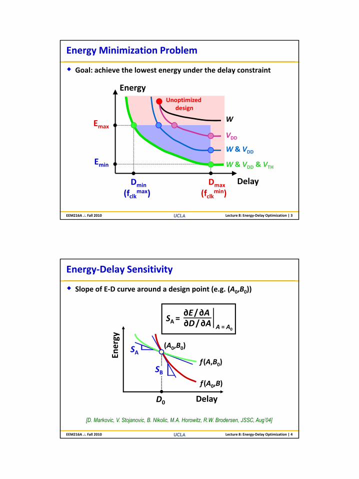
Energy Minimization Problem
Goal: achieve the lowest energy under the delay constraint
Unoptimized
EnergyUnoptimized
design
W
VDD
W & VDD
Emax
E
D. Markovic / Slide 3
Delay
W & VDD & VTH
DmaxDmin
Emin
(fclkmax) (fclk
min)
EEM216A .:. Fall 2010 Lecture 8: Energy‐Delay Optimization | 3
Energy‐Delay Sensitivity
Slope of E‐D curve around a design point (e.g. (A0,B0))
∂E/∂AS = ∂D/∂A A = A0
SA =
SB
SA
f (A,B0)
Ener
gy
(A0,B0)
D. Markovic / Slide 4
[D. Markovic, V. Stojanovic, B. Nikolic, M.A. Horowitz, R.W. Brodersen, JSSC, Aug’04]
f (A0,B)
DelayD0
EEM216A .:. Fall 2010 Lecture 8: Energy‐Delay Optimization | 4

3
Solution: Equal Sensitivities
A fixed point is reached when all sensitivities are equal
∆E = SA·(−∆D) + SB·∆Df (A B)
f (A,B0)
Ener
gy(A0,B0)
∆D
f (A1,B)
D. Markovic / Slide 5
f (A0,B)
DelayD0
∆D
EEM216A .:. Fall 2010 Lecture 8: Energy‐Delay Optimization | 5
Circuit Optimization
topology A
topology BEner
gy/o
p
Constraints
D. Markovic / Slide 6
Reference design− Dmin sizing @ VDD
max, VTHref
Delay
Goal: find optimal E‐D tradeoff for a
logic function
EEM216A .:. Fall 2010 Lecture 8: Energy‐Delay Optimization | 6

4
Alpha‐power based Delay Model
Combined with Logical Effort Formulation (*)
1.5
2
2.5
3
3.5
4
4 de
lay
(nor
m.)
Von = 0.37 Vαd = 1.53
simulationmodel Fitting parameters
− Von, αd, Kd
Effective fanout−
D. Markovic / Slide 7
0.5 0.6 0.7 0.8 0.9 1 0
0.5
1
Vdd / Vddref
FO4
(*) [Sutherland et al., Logical Effort, 1999]
VDDref = 1.2V, FO4 (VDD
ref) = 25ps
.
EEM216A .:. Fall 2010 Lecture 8: Energy‐Delay Optimization | 7
Energy Model
Switching energy
Leakage energy
D. Markovic / Slide 8
with:D: the cycle timeI0(Sin): normalized leakage current with inputs in state Sin
EEM216A .:. Fall 2010 Lecture 8: Energy‐Delay Optimization | 8

5
Adjusting Switching Energy of a Gate
,dd iV , 1dd iV +
i i+1
Wwirepnom,i WiWi
,
Wi+1
Wi
Wpar,i
Wout
Sizi
ng
Supp
ly
D. Markovic / Slide 9
= energy stored on the logic gate i
EEM216A .:. Fall 2010 Lecture 8: Energy‐Delay Optimization | 9
Optimization Setup
Reference/nominal circuit– Sized for Dmin @ VDD
nom
D fi d l t i t nerg
y reference
Define delay constraint– Dcon = Dmin (1 + dinc /100)
Minimize energy under delay constraint– VDD scaling (global, discrete, per‐stage)– Gate sizing (W)
Dmin Delay
En
D. Markovic / Slide 10
– Threshold adjustment (VTH)– Optional buffering
EEM216A .:. Fall 2010 Lecture 8: Energy‐Delay Optimization | 10

6
Profitability of Optimization (∂E/∂D)
Gate sizing (W)
∞ for equal heff
(Dmin)
Supply voltage (VDD)
VTH VDD
VDDref
S(V
DD)
D. Markovic / Slide 11
Threshold voltage (VTH)
0 VTH
VTHrefS(
VTH
)
EEM216A .:. Fall 2010 Lecture 8: Energy‐Delay Optimization | 11
Circuit Optimization Examples
Inverter chain
Memory decoderB hi
predecoder word driver
CL
− Branching− Inactive gates
Tree adder− Long wires− Re‐convergent paths
CL
3 15
CW
addrinput
wordline
m = 16 m = 4m = 2
m = 1n = 0 n = 12
n = 30n = 255
S15(A15, B15)
D. Markovic / Slide 12
− Multiple active outputs
S0(A0, B0)Cin
EEM216A .:. Fall 2010 Lecture 8: Energy‐Delay Optimization | 12

7
Example: Inverter Chain
Properties of inverter chain− Single path topology− Energy increases geometrically from input to output
CL1
W1 = 1 W2 … WNW3
Goal
D. Markovic / Slide 13
Goal− Find optimal sizing W = [W1, W2, …, WN], supply voltage, and
buffering strategy to achieve the best energy‐delay tradeoff
EEM216A .:. Fall 2010 Lecture 8: Energy‐Delay Optimization | 13
Inverter Chain: Gate Sizing & Buffering
[M F IEEE JSSC 9/94]
20
25
ut, h
eff
30%
dinc= 50%nomopt
[Ma, Franzon, IEEE JSSC, 9/94]
1 2 3 4 5 6 70
5
10
15
effe
ctiv
e fa
nou
0%
1%
10%
30%
D. Markovic / Slide 14
Variable taper achieves minimum energyReduce number of stages at large dinc
1 2 3 4 5 6 7stage
EEM216A .:. Fall 2010 Lecture 8: Energy‐Delay Optimization | 14

8
Inverter Chain: VDD Optimization
0 8
1.0
m
0%
1% 12
15
18
ut, h
eff
dinc= 50%nomopt
1 2 3 4 5 6 70
0.2
0.4
0.6
0.8
Vdd
/ V
ddnom 1%
10%30%
dinc= 50%
nomopt
1 2 3 4 5 6 70
3
6
9
12
effe
ctiv
e fa
nou
0%
1%10%
30%
D. Markovic / Slide 15
Variable taper achieved by voltage scalingVDD reduces energy of the final load first
1 2 3 4 5 6 7stage
1 2 3 4 5 6 7stage
EEM216A .:. Fall 2010 Lecture 8: Energy‐Delay Optimization | 15
Inverter Chain: Optimization Results
80
100
tion
(%) cW
gVdd2VddcVdd
0.8
1.0
norm
)
cWgVdd2Vdd
0 10 20 30 40 500
20
40
60
ener
gy re
duct
0 10 20 30 40 500
0.2
0.4
0.6
Sen
sitiv
ity (
D. Markovic / Slide 16
Parameter with the largest sensitivity has the largest potential for energy reductionTwo discrete supplies mimic per‐stage VDD
0 10 20 30 40 50dinc (%)
0 10 20 30 40 50dinc (%)
EEM216A .:. Fall 2010 Lecture 8: Energy‐Delay Optimization | 16

9
SRAM Decoder Energy Profile
Internal energy peak
80
100rm
)
0
20
40
60
Ener
gy (n
or
predecoder word driver
D. Markovic / Slide 17
CL
predecoder
3 15
CW
word driver
addrinput
wordline
m = 8 m = 4 m = 2 m = 1
EEM216A .:. Fall 2010 Lecture 8: Energy‐Delay Optimization | 17
W vs. VDD for Reducing Energy Peak
800
1000
800
1000 cW: E (-52%)2Vdd: E (-25%)Dmin,7
E d 10%
0
200
400
600
ener
gy
0
200
400
600
ener
gy
Dmin,7+5%E7 - 19%
E7 dinc=10%
D. Markovic / Slide 18
VDD less effective than W optimizationBuffering also reduces energy peak
1 2 3 4 5 6 7 8 9stage
1 2 3 4 5 6 7 8 9stage
[B. Amrutur, Ph.D. Thesis, Stanford, 8/99]
EEM216A .:. Fall 2010 Lecture 8: Energy‐Delay Optimization | 18

10
Tree Adder: Optimization Results
Reference: all paths are critical
Sizing Opt.1.1Dmin, 0.45Eref
referenceDmin, Eref
2‐VDD Opt.1.1Dmin, 0.73Eref
D. Markovic / Slide 19
Internal energy → W more effective than VDD
− For dinc = 10%: ∆EW = −55%, ∆E2Vdd = −27%
EEM216A .:. Fall 2010 Lecture 8: Energy‐Delay Optimization | 19
A Look at Tuning Variables…
10% excess delay → 30‐70% energy reduction
4
105
(Vthmin)
100 solid: inverter chaindashed: 8/256 decoder dotted: 64 bit adder
101
102
103
104
Sen
sitiv
ity
Vth
Vdd
W
(Vdd max)
(Vthref)
20
40
60
80
Ene
rgy
redu
ctio
n (%
)
W
Vdd Vth
dotted: 64-bit adder
D. Markovic / Slide 20
0.5 0.75 1 1.25 1.510
0
D / Dref
0 20 40 60 80 1000
Delay increase (%)
Peak performance is very power inefficient!
EEM216A .:. Fall 2010 Lecture 8: Energy‐Delay Optimization | 20

11
Circuit‐Level Results: Tree Adder
Result of joint (VDD, VTH, W) optimization:
SW=22SVth=22
SW→∞SVth=0.2SVdd=1.5
1.5
1 f − 65% of energy saved without delay penalty
− 25% better delay without energy cost
SVth 22SVdd=16
SW=1SVth=1SVdd=1
E/E re
f
0 0 5 1 1 5
1
0.5
0
65%
ref
D. Markovic / Slide 21
[D. Markovic , V. Stojanovic, B. Nikolic, M.A. Horowitz, R.W. Brodersen, JSSC, Aug’04]
Limited range of efficient circuit optimization
D/Dref
0 0.5 1 1.5
EEM216A .:. Fall 2010 Lecture 8: Energy‐Delay Optimization | 21
A Look at Tuning Variables
It is best when variables don’t reach their boundary values
reliability Sens(VDD) =
Supply voltage Threshold voltage1.75 0
reliabilitylimit
Sens(VDD) Sens(W) =Sens(VTH) = 1
0 25
0.5
0.75
1
1.25
1.5
VD
D/
VD
Dre
f
−300
−250
−200
−150
−100
50
∆V
TH(m
V)
D. Markovic / Slide 22
Limited range of tuning variables
−50 −25 0 25 50 75 100
Delay increment (%)
0
0.25
−50 −25 0 25 50 75 100
Delay increment (%)
−350
−300
EEM216A .:. Fall 2010 Lecture 8: Energy‐Delay Optimization | 22

12
A Look at Tuning Variables
When a variable reaches bound, fewer variables to work with
reliability Sens(VDD) =1.75 0
Supply voltage Threshold voltage
Sens(VDD) = 16Sens(VTH) =Sens(W) = 22
reliabilitylimit
Sens(VDD) Sens(W) =Sens(VTH) = 1
0 25
0.5
0.75
1
1.25
1.5
VD
D/
VD
Dre
f
−300
−250
−200
−150
−100
50
∆V
TH(m
V)
D. Markovic / Slide 23
Limited range of tuning variables
( DD) Sens(W)
−50 −25 0 25 50 75 100
Delay increment (%)
0
0.25
−50 −25 0 25 50 75 100
Delay increment (%)
−350
−300
EEM216A .:. Fall 2010 Lecture 8: Energy‐Delay Optimization | 23
Tree Adder: Joint Optimization
80
100
on (%
)
40
50
%) @
Dm
in
67%
lure
42%
0 20 40 60 80 1000
20
40
60
ener
gy re
duct
io
2Vdd + cW2VddgVdd + cWgVddcW
1 0 1 150
10
20
30
ener
gy re
duct
ion
(%
Dev
ice
fai
D. Markovic / Slide 24
Choose a more efficient variableHigher VDD yields a lower energy solution
0 20 40 60 80 100dinc (%)
1.0 1.15Vdd / Vdd
nom
EEM216A .:. Fall 2010 Lecture 8: Energy‐Delay Optimization | 24

13
An Update: Slope‐Aware Delay Model
LE overestimates delay– Assumes equal slopes
Add slope correctionK t & V d d t
D. Markovic / Slide 25
1 1
1
Ni i i i
i i ii i
g h g hD g h pK
− −
=
⋅ − ⋅= ⋅ + −
∑
– Ki: gate & VDD dependent
EEM216A .:. Fall 2010 Lecture 8: Energy‐Delay Optimization | 25
Result: Adder Example
16‐bits, output load: CL = 512 fF (total FO ~ 256)– Logical Effort: largely overestimates non‐critical paths
50 SimulationA
35
40
45
rnal
pow
er (µ
W)
Synthesized Adder
MatlabOptimized
Adders
LE with Slope CorrSynthesis TimingOriginal LE Model
A
B
D. Markovic / Slide 26
0.8 1 1.2 1.4 1.6 1.8 225
30
Delay (normalized to the synthesized adder)
Inte
r
EEM216A .:. Fall 2010 Lecture 8: Energy‐Delay Optimization | 26
[C.C. Wang, D. Markovic ,
TCAS-II, Aug’09]

14
Lessons from Circuit Optimization
Sensitivity‐based optimization framework– Equal marginal costs Energy‐efficient design– To reduce energy, it is not always best to reduce VDD
Effectiveness of tuning variables– Sizing is the most effective for small delay increments– Vdd is better for large delay increments
Peak performance is VERY power inefficient– About 70% energy reduction for 20% delay penalty
D. Markovic / Slide 27
gy y p y
Limited performance range of tuning variables– Additional variables for higher energy‐efficiency
EEM216A .:. Fall 2010 Lecture 8: Energy‐Delay Optimization | 27
Choosing Circuit Topology: Optimal Register?
64‐bit ALUREG
REG
AddCL=32
Cin=2
Cin=1
b=8
Add
in
DQCp
S
Cp
CpD
QClk ClkQMSM
Clk1SS
Clk1
Clk1
Clk1Clk
Clk
Clk1Clk
D. Markovic / Slide 28
(a) Cycle-latch (CL) (b) Static Master-slave Latch-pair (SMS)Cycle‐latch (CL) Static Master‐Slave Latch‐Pair (SMS)
Given energy‐delay tradeoff for adder and register (two register options), what is the best energy‐delay tradeoff in the ALU?
EEM216A .:. Fall 2010 Lecture 8: Energy‐Delay Optimization | 28

15
Balancing Sensitivity Across Circuit Blocks
Upsize lower activity blocks (Add) to save energy
2.5 ALU
y
Add
1
1.5
2
Ene
rgy
(nor
m.)
Reg
Add
S Reg
Ener
gy
Reg
D. Markovic / Slide 29
0 5 10 15 20 250
0.5CL SMS
Delay (FO4)
SMSCL
S Add
= S
EEM216A .:. Fall 2010 Lecture 8: Energy‐Delay Optimization | 29
Micro‐Architectural Optimization
throughput# of bits
interleaving
Macro Arch.Macro Arch.
delay
throughput
par, t-mux
cct topology
E-D tradeoff
algorithm
EEparallelpipelinetime-mux
interleavingfolding
AreaMicro Arch.Micro Arch.
D. Markovic / Slide 30
E-D trade-offVdd, Vth, W
EEWVthVdd
time mux
CircuitCircuit
EEM216A .:. Fall 2010 Lecture 8: Energy‐Delay Optimization | 30

16
Reducing the Supply Voltage
(while maintaining performance) Concurrency:trading off clock frequency versus area to reduce power
F1
Reference design
F2
R
R
R
R: register, F1,F2: combinational logic(adders, ALUs, etc)
D. Markovic / Slide 31
fref
Cref: average switching capacitance
[Chandrakasan et al., JSSC’92]
EEM216A .:. Fall 2010 Lecture 8: Energy‐Delay Optimization | 31
A Parallel Implementation
Running slower lowers required VDD (quadratic power reduction)
F1R
F1F2R
R
fref /2
F1R
Almost cancels
D. Markovic / Slide 32
F1F2R
R
fref /2
EEM216A .:. Fall 2010 Lecture 8: Energy‐Delay Optimization | 32

17
Parallelism Example (90nm CMOS)
Power (assuming ovpar = 7.5%)
4.5
5
1 5
2
2.5
3
3.5
4
t p(n
orm
.)
D. Markovic / Slide 33
From J. Rabaey (UCB)0.5 0.6 0.7 0.8 0.9 11
1.5
VDD (norm.)
How many levels of parallelism?
EEM216A .:. Fall 2010 Lecture 8: Energy‐Delay Optimization | 33
The More Parallel the Better?
Tota
l Ene
rgy
Reference
ParallelFrom J. Rabaey (UCB)
D. Markovic / Slide 34
Supply voltage, VDD
EEM216A .:. Fall 2010
Leakage and overhead start to dominate at high levels of parallelism, causing min E to increaseOptimum voltage also increases with parallelism
Lecture 8: Energy‐Delay Optimization | 34

18
Increasing use of Concurrency Saturates
PFixedThroughput
Nominal design(no concurrency)
g p
Concurrency
Pmin
Overhead +leakage
D. Markovic / Slide 35
Only option: Reduce VTH as well!But: Must consider Leakage …
VDD From J. Rabaey (UCB)
EEM216A .:. Fall 2010 Lecture 8: Energy‐Delay Optimization | 35
A Pipelined Implementation
Shallower logic reduces required supply voltage
F1R
RF1
F2R
R
fref
R
R
fref
/
D. Markovic / Slide 36
Assumingovpipe = 10%
This example assumes equal VDD for par / pipe designs
EEM216A .:. Fall 2010 Lecture 8: Energy‐Delay Optimization | 36

19
Mapping into the Energy‐Delay Space
E Op
referenceP = 2P = 3P = 4
Energy‐delay for ALU realizations with varying parallelism
P = 4P = 5
Increasing parallelism (P)
Fixed throughput
Minimum EDP
D. Markovic / Slide 37
Level of concurrency depends on target performanceRule of thumb: If speed exceeds MEP point, add parallelism
Delay = 1/Throughput
EEM216A .:. Fall 2010 Lecture 8: Energy‐Delay Optimization | 37
Leakage is Not Necessarily a Bad Thing
EOp for three architectures (ref, par, pipe) of ALU– Set VTH, adjust VDD to maintain performance, plot Eop
1
0 2
0.4
0.6
0.8
EO
p / no
min
al E
Op
ref
nominal
Vthref-180mV
0.81Vddmax
Vthref-95mV
0.57Vddmax
V href-140mV
Topology Inv Add Dec
(E /E )opt 0 8 0 5 0 2
D. Markovic / Slide 38
10-2
10-1
100
101
0
0.2
ELeakage/ESwitching
parallelpipeline
Vth 140mV0.52Vdd
max (ELk/ESw)opt 0.8 0.5 0.2
Optimal designs have high leakage (ELk/ESw ≈ 0.5)!
Adapt to process and activity variations
EEM216A .:. Fall 2010 Lecture 8: Energy‐Delay Optimization | 38

20
Parallelism and Pipelining in E‐D Space
2f
(a) reference
A B
A B B
BA
A
f f
f
reference
2f
(c) pipeline (b) parallel
A B BAf f f
parallelpipelineer
gy/O
p It is important to linkback to E‐D tradeoff
D. Markovic / Slide 39
reference parallel/pipeline
Time/Op
Ene
EEM216A .:. Fall 2010 Lecture 8: Energy‐Delay Optimization | 39
Time Multiplexing
Af f
AAf f
time‐mux
(a) reference for time-mux (b) time-multiplex
Af f f f
2f 2f
time‐muxreference
gy/O
p
For throughputs below min EDP:Absorb unused time slack by increasing Clk freq. (and VDD)
D. Markovic / Slide 40
reference
Time/Op
Ener
g increasing Clk freq. (and VDD)Again comes with some area and capacitance overhead
EEM216A .:. Fall 2010 Lecture 8: Energy‐Delay Optimization | 40

21
Energy‐Area Tradeoff
1 1 1234 64‐b ALU
High throughput: Parallelism = Large Area
Max Eop
1 12
13
14 1
5
A = Aref15
f1
D. Markovic / Slide 41
Ttarget
A = Aref13
Low throughput: Time‐Mux = Small AreaEEM216A .:. Fall 2010 Lecture 8: Energy‐Delay Optimization | 41
Putting it All Together
Balance logic depth (Ld) within a block, adjust latency to reach TClk
Apply VDD and W optimization to the underlying pipelines
Circuit (datapath)Micro Arch. (block)
Ld
SpeedPowerArea
Ener
gy
Wopt @ VDDrefW
Min delaySW=∞,SVdd =2
SW=SVdd =2
Target delay
Late
ncy
D. Markovic / Slide 42EEM216A .:. Fall 2010
Delay0
Target delaySW=SVdd <2
VDD
scaling
Cycle time (TClk)0
VDD
Wmult
add
Lecture 8: Energy‐Delay Optimization | 42

22
Motivation for System Level Optimization
Optimizations at the architecture or system level can enable more effective power minimization at the circuit level (while maintaining performance), such as
Enabling a reduction in supply voltage– Enabling a reduction in supply voltage– Reducing the effective switching capacitance for a given
function (physical capacitance, activity)– Reducing the switching rates– Reducing leakage
Optimizations at higher abstraction levels tend to have greater
D. Markovic / Slide 43
Optimizations at higher abstraction levels tend to have greater potential impact– While circuit techniques may yield improvements in the 10‐50%
range, architecture and algorithm optimizations have reported orders of magnitude power reduction
EEM216A .:. Fall 2010 Lecture 8: Energy‐Delay Optimization | 43
Some Energy‐Inspired Design Guidelines
For maximum performance– Maximize use of concurrency at the cost of area
For given performanceFor given performance– Optimal amount of concurrency for minimum energy
For given energy – Least amount of concurrency that meets performance goals
For minimum energy
D. Markovic / Slide 44
For minimum energy– Solution with minimum overhead
(direct mapping between function and architecture)
EEM216A .:. Fall 2010 Lecture 8: Energy‐Delay Optimization | 44