end-of-semester examination - international …staff.iium.edu.my/adah510/final exam...
TRANSCRIPT

KULLIYYAH OF ENGINEERING
END-OF-SEMESTER EXAMINATIONSEMESTER 1, 2015/2016 SESSION
Programme : Engineering Level of Study : UG 1Time : 9.00 am -12.00 pm Date : 03/01/2016Duration : 3 HrsCourse Code : ECE 1312/EECE 1312 Section(s) : 1- 5Course Title : Electronics
This Question Paper Consists of 12 (Twelve) Printed Pages (Including Cover Page) with 5 (Five) Questions.
INSTRUCTION(S) TO CANDIDATES
DO NOT OPEN UNTIL YOU ARE ASKED TO DO SO
Total mark of this examination is 100. This examination is worth 50 % of the total course assessment. Answer ALL QUESTIONS Only approved calculator with ‘KoE approved’ sticker is allowed (non-programmable and
non-graphical). Marks assigned to each problem are listed in the margins.
Any forms of cheating or attempt to cheat is a serious offence which may lead to dismissal.
All electronics gadgets are prohibited in the exam hall / venue.(e.g. mobile / smart phones, smart watches, and smart glasses)
APPROVED BY:
1

QUESTION 1 (20 marks)
a) A solar cell is a special type of pn-junction diode. The current equation of a particular solar cell is represented as follows:
I D=5.0×10⁻¹³[e(V D
V T)−1]−7.7×10⁻² (A)
When the cell is irradiated with sunlight and the cell current, I D=0, the voltage V Dis referred to as the open circuit voltage, V OC. Similarly, when the cell is irradiated in the sunlight and the cell voltage, V D=0, the current I Dat that time is called the short circuit current, I SC. If the cell is operating at room temperature determine the parameters of the solar cell as follows: (4 + 2 marks)
i. Open circuit voltage, V OC
ii. Short circuit current, I SC
b) Consider the circuit shown in Fig. 1(b). The diode cut-in voltage is V γ=0.7V . Calculate the output voltage vO and plot it with respect to the input voltage v I in the same time
scale over the range of voltages −10V ≤ v I ≤ +10V for V B=5V. (4 marks)
Fig. 1(b)
2

c) A clamper circuit is shown in Fig. 1(c). Write the equation of input-output voltage relation of the circuit. Sketch the output voltage waveform, vOagainst the time, t, if the input has sinusoidal voltage, vI=6 sin ( ωt )V and diode cut-in voltage, V γ=0V . (4 marks)
Fig. 1(c)
d) In the circuit shown in Fig. 1(d), the power rating of the Zener diode is 4W . Let, V I=58V , R i=150Ω ,V Z=16V and the minimum diode current is 15mA. (2 + 4 marks)
i. Determine the range of the diode current
ii. Determine the range of the load resistance, RL
Fig. 1(d)
QUESTION 2 (20 marks)
3

a) Consider the circuit shown in Fig. 2(a). Assume that V CC=2.8V ,β=180andV BE (on )=0.7V . Design the circuit by finding the values of RBand RCsuch thatI C=0.12mA and V CE=1.4V . (6 marks)
Fig. 2(a)
b) A transistor has current gain, β in the range of 90≤ β ≤180 and the collector current, I C is in the range of 0.8mA ≤ IC ≤1.2mA. What is the possible range of gmandr π? Assume that V T=0.026V . (5 marks)
4

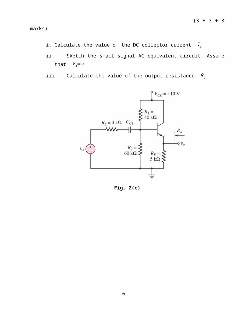
c) A common collector circuit is shown in Fig. 2(c). Given that = 100. Assume V BE (on )=0.7V . (3 + 3 + 3 marks)
i. Calculate the value of the DC collector current I C
ii. Sketch the small signal AC equivalent circuit. Assume that V A=∞
iii. Calculate the value of the output resistance RO
Fig. 2(c)
5
QUESTION 3 (20 marks)
a) A transistor transconductance, gm=50mA /V and emitter resistancer π=1.5kΩwhen it is operating at room temperature. Determine the collector current I CQ and common emitter-current gain β of the transistor. Assume that V T=0.026V . (4 marks)
b) A common-emitter amplifier has output voltage −2.4V when its input voltage is 250mV . The collector resistance of the amplifier has 1.5kΩis changed to 2.5kΩ, what is the new voltage gain of the amplifier ? Consider that rO=∞.
(5 marks)
c) For the common emitter circuit in Fig. 3(c), the transistor parameters are β=100 and V A=∞. The parameters of the circuit are V BE (on )=0.7V , I C=0.5mA and V CE=3V . (5 + 2 + 4 marks)
i. Find the value of REand RC
ii. Draw the small-signal equivalent circuit
iii. Determine the value of the voltage gain, Av=vO /vS
6

Fig. 3(c)
7

QUESTION 4 (20 marks)
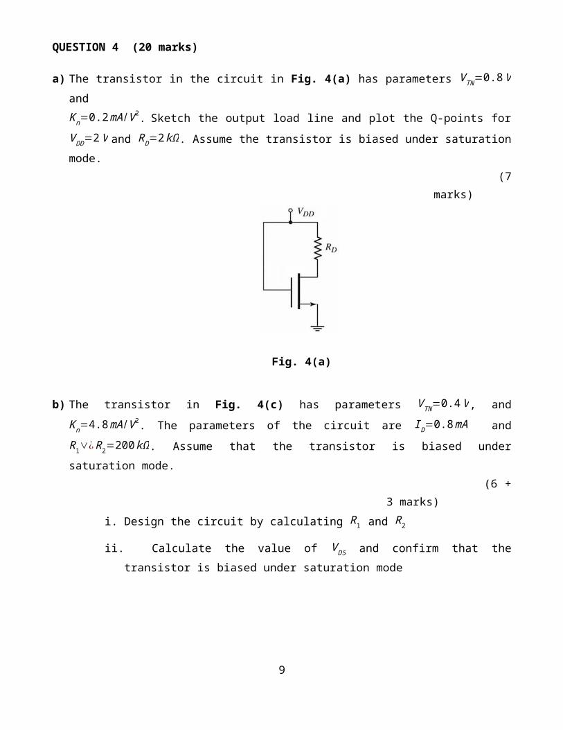
a) The transistor in the circuit in Fig. 4(a) has parameters V TN=0.8V and
Kn=0.2mA /V 2. Sketch the output load line and plot the Q-points for V DD=2V and RD=2kΩ. Assume the transistor is biased under saturation mode.
(7 marks)
Fig. 4(a)
b) The transistor in Fig. 4(c) has parameters V TN=0.4V , and Kn=4.8mA /V 2. The parameters of the circuit are I D=0.8mA and R1∨¿ R2=200kΩ. Assume that the transistor is biased under saturation mode.
(6 + 3 marks)i. Design the circuit by calculating R1 and R2
ii. Calculate the value of V DS and confirm that the transistor is biased under saturation mode
Fig. 4(c)
8
c) For an NMOS biased in the saturation region, the parameters are K n' =0.1mA /V 2,
V TN=1.2V and I D=0.8mA. Determine the transistor width to length ratio (W /L ) such that gm=1.8mA /V . (4 marks)
9

QUESTION 5 (20 marks)
a) The parameters of the common source circuit shown in Fig. 5(a) are V DD=12 ,RD=3 kΩ, RS=0.5kΩ , R1=894 kΩ , R2=347 kΩ and RL=10kΩ. The transistor parameters are, V TN=1.2V , Kn=1.5mA /V 2and λ=0.
(6 + 5 marks)
i. Find the values of I D and V DS
ii. Determine the input resistance, R¿ and the small-signal voltage gain, A v
Fig. 5(a)
b) Determine the output voltage vO for vI=3V for the op-amp circuit shown in Fig. 5(b). Then, calculate the output current that flows through 5kΩ resistor.
10

(4 marks)
Fig. 5(b)
c) For the inverting summing amplifier shown in Fig. 5(c), determine the value of R3 if all the circuit parameters are given as: R1=50kΩ , R2=40kΩ, RF=50 kΩ and vO=−10V . The inputs to the circuit are, vI 1=1V , vI 2=2V and v I 3=0.3V .
(5 marks)
Fig. 5(c)Some Useful Equations
Equation for pn- junction:
11

Equations for BJT
Equations for MOSFET
Kn=k n
'
2WL
END OF PAPER
12
ID=I s(e
v D
V T −1)
gm=ICQ
V T
r π=β V T
I CQgm rπ=β
ro=V A
I CQ
I D=Kn [2 (V GS−V TN ) V DS−VDS2
]
ID=Kn (V GS−V TN )2
ro=V A
I DQ= 1
λ IDQ
λ= 1V A
gm=2√Kn I DQ