enabling parallel testing at sort for high power … · enabling parallel testing at sort ... zthis...
TRANSCRIPT

Enabling Parallel Testing at Sort Enabling Parallel Testing at Sort for High Power Productsfor High Power Products
Abdel AbdelrahmanAbdel Abdelrahman
Tim SwettlenTim Swettlen
2200 Mission College Blvd.2200 Mission College Blvd.
M/S SC2M/S SC2--0707
Santa Clara, CA 94536Santa Clara, CA 94536
[email protected]@intel.com
[email protected]@intel.com

2 2002
AgendaAgenda
BackgroundBackgroundGoals:Goals:
–– Interchangeability between a 1X and 2X SIU Interchangeability between a 1X and 2X SIU –– Equivalent performance between a 1X SIU and a 2X SIU Equivalent performance between a 1X SIU and a 2X SIU –– Equivalent performance between “test site 1” and “test site 2” oEquivalent performance between “test site 1” and “test site 2” on the 2X n the 2X
SIUSIU
ChallengesChallenges–– Spatial Location of 2 Spatial Location of 2 DUTsDUTs–– Space TransformerSpace Transformer–– Printed Circuit Board (PCB)Printed Circuit Board (PCB)–– Interconnect and stiffening HardwareInterconnect and stiffening Hardware
ResultsResultsMinimal DeflectionsMinimal DeflectionsPower deliveryPower deliverySignal IntegritySignal IntegritySummarySummary

3 2002
BackgroundBackground
Parallel Testing is a manufacturing capability that allows multiParallel Testing is a manufacturing capability that allows multiple ple devices to be tested simultaneously.devices to be tested simultaneously.
Parallel testing allows the user to improve output capacity of eParallel testing allows the user to improve output capacity of each ach test module by reducing the average test timetest module by reducing the average test time
Capability has existed at Intel for Flash Memory products since Capability has existed at Intel for Flash Memory products since 1989.1989.
For High Power CPUs parallel testing (2X) aims to test 2 die at For High Power CPUs parallel testing (2X) aims to test 2 die at a a time.time.
Testing 2 CPUs at one time has been more challenging due to the Testing 2 CPUs at one time has been more challenging due to the high power demand and the complexity of the probe card designhigh power demand and the complexity of the probe card design
This presentation focuses on the work done to demonstrate the 2XThis presentation focuses on the work done to demonstrate the 2Xprobe card capability being applied to microprocessorsprobe card capability being applied to microprocessors

4 2002
Project GoalProject Goal
GOAL:GOAL:–– To develop a robust 2X Sort Interface Unit (SIU) capable of To develop a robust 2X Sort Interface Unit (SIU) capable of
intercepting high power microprocessors intercepting high power microprocessors
Fundamental criteria:Fundamental criteria:Interchangeability and equivalent performance between the 1X andInterchangeability and equivalent performance between the 1X andthe 2X SIUthe 2X SIU
-- To eliminate the need to segregate test modulesTo eliminate the need to segregate test modules-- To increase cost savingsTo increase cost savings
Equivalent performance between “test site 1” and “test site 2” oEquivalent performance between “test site 1” and “test site 2” on n the 2X SIUthe 2X SIU
–– To reduce test pattern developmentTo reduce test pattern development
Boundary conditionsBoundary conditions–– Similar shape, size and functionality of the probe cardSimilar shape, size and functionality of the probe card–– Equivalent power delivery and routing integrityEquivalent power delivery and routing integrity

5 2002
Magnitude of change ChallengesChallenges
A.A. New StiffenerNew Stiffener: To accommodate larger MLC: To accommodate larger MLC
B.B. Bulk decouplingBulk decoupling: New location and improved components: New location and improved components
C.C. PCBPCB: Split power planes for isolation: Split power planes for isolation
D.D. InterconnectInterconnect: Increase in physical size and LGA count: Increase in physical size and LGA count
E.E. Space TransformerSpace Transformer: Split plans, new stack, larger in size: Split plans, new stack, larger in size
F.F. ProbesProbes: Same as current probe selection, but marginal increase : Same as current probe selection, but marginal increase in total probe countin total probe count
Minor
Minor
Mix
Major
Major
Minor
Top-side Stiffening Hardware
PCB
CeramicStiffener plate
MountingBlock
A
B
C
D
E
F
Wafer

6 2002
Comparison of noted 1X and 2X SIU differencesComparison of noted 1X and 2X SIU differences
24240.1870.187””> 2500 total> 2500 total
~ 250 total ~ 250 total 1 layer Thin Film1 layer Thin Film3.5 x 3.5 x 0.1503.5 x 3.5 x 0.150””~ 180 caps total~ 180 caps total
~ 3200 total~ 3200 total
2X 2X ConfigurationConfiguration
22220.1870.187””> 2500 total> 2500 total
22220.1870.187””~ 1300 total~ 1300 total
Printed Circuit BoardPrinted Circuit Board
# of layers # of layers
ThicknessThickness
LGALGA
~ 300 total~ 300 totalMixedMixed2.5 x 2.5 x 0.1502.5 x 2.5 x 0.150””~ 90 caps~ 90 caps
~ 125 total~ 125 total2 layers ceramic2 layers ceramic2.5 x 2.5 x 0.1502.5 x 2.5 x 0.150””~ 90 caps total~ 90 caps total
Glass Ceramic STGlass Ceramic ST
# of I/Os# of I/Os
Routing TechnologyRouting Technology
DimensionsDimensions
DecouplingDecoupling
~ 3000 total~ 3000 total~ 1600 total~ 1600 totalWafer Level contactsWafer Level contacts
# of contacts# of contacts
1X 1X EnvelopeEnvelope
1X 1X Configuration Configuration
Noted DifferencesNoted DifferencesShort listShort list

7 2002
Thin Film Space TransformerThin Film Space Transformer
Equivalent performance challenges most pronounced in STEquivalent performance challenges most pronounced in STPower delivery of ~ 60 W per DUTPower delivery of ~ 60 W per DUT
–– Larger space to allow adequate decoupling and power plane area.Larger space to allow adequate decoupling and power plane area.Signal routing: escape routing of 128 channels per designSignal routing: escape routing of 128 channels per design
–– Thin Film allows fine line widths to be fabricated.Thin Film allows fine line widths to be fabricated.A2/B1 alternatives: More space w/ constraints: scribe width, plaA2/B1 alternatives: More space w/ constraints: scribe width, planaritynarity
2.5”
3.5”1 DIE
A2
B1
LGAs
CAPs

8 2002
Interconnect and Space Transformer (ST)Interconnect and Space Transformer (ST)
ST area would be increased by ~80%ST area would be increased by ~80%–– Increased LGA count to >2500 at the PCB interfaceIncreased LGA count to >2500 at the PCB interface
–– Required development of an interconnect solutionRequired development of an interconnect solution
ST would need to provide independent power delivery ST would need to provide independent power delivery systemssystems
–– No shared power planesNo shared power planes
–– No shared reference (Ground) planesNo shared reference (Ground) planes
–– Routing rules needed to be defined to maintain Signal integrityRouting rules needed to be defined to maintain Signal integrity
–– Increased # of decoupling capacitors, locations not as idealIncreased # of decoupling capacitors, locations not as ideal
Location of two DUT arrays given the above constraintsLocation of two DUT arrays given the above constraints–– Where to locate the two arrays with respect to each otherWhere to locate the two arrays with respect to each other

9 2002
Spatial Location of the two Spatial Location of the two DUT’sDUT’s
Flexibility in choiceFlexibility in choice–– A 3x3 maximum array area was assumed possibleA 3x3 maximum array area was assumed possible
Trade off analysis: SIU manufacturing, routing, power Trade off analysis: SIU manufacturing, routing, power delivery, die isolation, heat dissipation and a sort dedelivery, die isolation, heat dissipation and a sort de--rating rating study that considered wafer stepping impacts with different study that considered wafer stepping impacts with different patterns patterns
A diagonal sideA diagonal side--byby--side side pattern was considered to pattern was considered to be the best solution to all be the best solution to all constraintsconstraints
–– Sites A2/B1Sites A2/B1
Splitting the power planesSplitting the power planes–– Consider power deliveryConsider power delivery
–– Consider decouplingConsider decoupling
A1 A2 A3
B1 B2 B3
C1 C2 C3
S.T.
A2/B1 Design
OR
10 2002
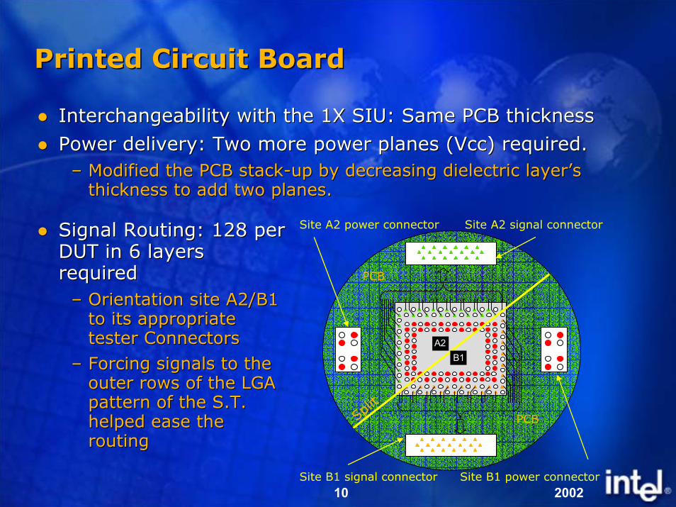
Printed Circuit BoardPrinted Circuit Board
Interchangeability with the 1X SIU: Same PCB thicknessInterchangeability with the 1X SIU: Same PCB thickness
Power delivery: Two more power planes (Power delivery: Two more power planes (VccVcc) required.) required.–– Modified the PCB stackModified the PCB stack--up by decreasing dielectric layer’s up by decreasing dielectric layer’s
thickness to add two planes.thickness to add two planes.
Signal Routing: 128 per Signal Routing: 128 per DUT in 6 layers DUT in 6 layers requiredrequired
–– Orientation site A2/B1 Orientation site A2/B1 to its appropriate to its appropriate tester Connectorstester Connectors
–– Forcing signals to the Forcing signals to the outer rows of the LGA outer rows of the LGA pattern of the S.T. pattern of the S.T. helped ease the helped ease the routing
Site A2 power connector Site A2 signal connector
Site B1 power connectorSite B1 signal connector
Split
PCB
PCB
A2B1
routing

11 2002
Interconnect Solution SelectionInterconnect Solution Selection
Trade off analysis: Reflow Trade off analysis: Reflow Heat, CTE mismatch, planarity and Heat, CTE mismatch, planarity and thinner STthinner ST
NoNoYes Yes YesYes50 mil pitch 50 mil pitch achievable achievable
YesYesYesYesNoNoCompatibility Compatibility w/thinner STw/thinner ST
< 2.0 mils< 2.0 mils< 2.0 mils< 2.0 mils< 2.0 mils< 2.0 milsPlanarity Planarity improvement improvement
Up to 800 CUp to 800 CUp to 225 CUp to 225 CN/AN/AHeat to attach Heat to attach pins/ballspins/balls
Pin Grid Array Pin Grid Array of gold plated of gold plated Kovar pinsKovar pins
Ball Grid Array Ball Grid Array of Pb/Sn solder of Pb/Sn solder ballsballs
Pogo interposerPogo interposerWhat it is What it is
PGAPGABGABGAButtonButton
InterposerInterposerInterconnectInterconnect

12 2002
PCB Mechanical stiffenerPCB Mechanical stiffener
Requirements to meet: Requirements to meet: --Fit in a larger STFit in a larger ST
--Increase ID of mounting hardware keep out zoneIncrease ID of mounting hardware keep out zone
--Limit 2X stiffener thickness changes to control/reduce deflectioLimit 2X stiffener thickness changes to control/reduce deflectionn
--Maintain clearance for tester cable connections. Maintain clearance for tester cable connections.
ID
Clearance

13 2002
Deflection DataDeflection Data
Preliminary data collected on 1 tool, using a deflection Preliminary data collected on 1 tool, using a deflection measurement system, show signs of reduced deflection.measurement system, show signs of reduced deflection.
More data needed More data needed to improve to improve accuracy of best fit accuracy of best fit line (Rline (R22) and to ) and to better assess better assess repeatability and repeatability and reproducibilityreproducibility

14 2002
The Measurements… what we didThe Measurements… what we did
8 measurement points8 measurement points–– 4 per DUT4 per DUT
–– Measure voltage at the DUTMeasure voltage at the DUT
–– Provide ability to block nonProvide ability to block non--uniform demand of the DUTuniform demand of the DUT
Measured withMeasured with–– Site 1 “ON” and Site 2 “ON”Site 1 “ON” and Site 2 “ON”
–– Site 1 “ON” and Site 2 “OFF”Site 1 “ON” and Site 2 “OFF”
–– Site 1 “OFF” and Site 2 “ON”J3 J4
J5 J6J9 J10
J11 J12
Site 1 “OFF” and Site 2 “ON”

15 2002
Performance ResultsPerformance Results
Within site a large variance, but site to site well matchedWithin site a large variance, but site to site well matched
J3 J4
J5 J6J9 J10
J11 J12
J3 & J9
J6 & J12
T I M E
VOLT
AG
E
Site 1 = “ON”Site 2 = “ON”
DUT running > 1.0 GHz

16 2002
Performance Results, Cross talkPerformance Results, Cross talkNo measurable coupling of energy between sitesNo measurable coupling of energy between sites
J3 J4
J5 J6J9 J10
J11 J12
T I M E
VOLT
AG
E
J9J11
J6Plotted on Right scale
Site 1 = “OFF”Site 2 = “ON”
DUT running > 1.0 GHz
0 V; no energy coupled site to site

17 2002
Performance Results, Cross talkPerformance Results, Cross talkNo measurable coupling of energy between sitesNo measurable coupling of energy between sites
J4J6
J9Plotted on Right scale
J3 J4
J5 J6J9 J10
J11 J12
T I M E
VOLT
AG
E
Site 1 = “ON”Site 2 = “OFF”
DUT running > 1.0 GHz
0 V; no energy coupled site to site

18 2002
Signal integrity between sitesSignal integrity between sites
TDR of 10 traces on both sitesTDR of 10 traces on both sites–– Lengths are different, but this is compensated by the ATELengths are different, but this is compensated by the ATE
–– Worst channels shownWorst channels shown
Site 210 channels
Site 110 channels
Comparable magnitudes

19 2002
SummarySummary
To date the 2X SIU development is progressing at or beyond To date the 2X SIU development is progressing at or beyond expectationsexpectations
–– Metrology system check out passed with no issuesMetrology system check out passed with no issues
–– Sort performance data shows 2X card progressing wellSort performance data shows 2X card progressing well–– Small “hickSmall “hick--ups” still need to be worked onups” still need to be worked on
–– Improvements to the SI path planned, but not critical (yet) Improvements to the SI path planned, but not critical (yet)
–– More characterization work to be completedMore characterization work to be completed
–– Progressing well against slide four goalsProgressing well against slide four goals

20 2002
AcknowledgementAcknowledgement
Many thanks to Eugene Doan, Bau Nguyen, Thuy Pham and Many thanks to Eugene Doan, Bau Nguyen, Thuy Pham and Kevin Zhu for all the efforts spent on the 2X projectKevin Zhu for all the efforts spent on the 2X project
Thanks to the ITTO team for the feedback and making sure Thanks to the ITTO team for the feedback and making sure the paper wasn’t too boringthe paper wasn’t too boring
Thank YOU!