en / acs880 igbt supply control program firmware …...abb industrial drives acs880 igbt supply...
TRANSCRIPT

—ABB INDUSTRIAL DRIVES
ACS880 IGBT supply control programFirmware manual
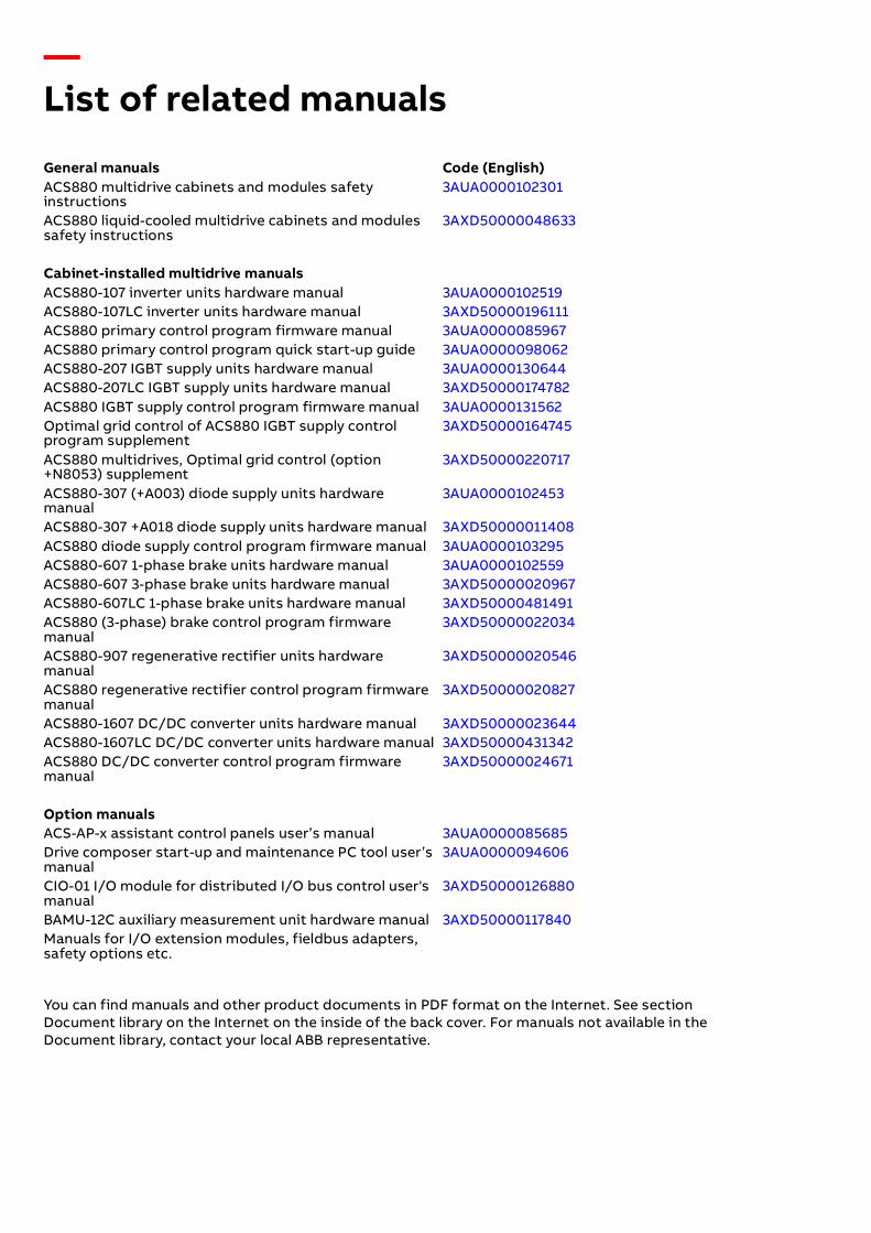
—List of related manuals
You can find manuals and other product documents in PDF format on the Internet. See section Document library on the Internet on the inside of the back cover. For manuals not available in the Document library, contact your local ABB representative.
General manuals Code (English)ACS880 multidrive cabinets and modules safety instructions
3AUA0000102301
ACS880 liquid-cooled multidrive cabinets and modules safety instructions
3AXD50000048633
Cabinet-installed multidrive manualsACS880-107 inverter units hardware manual 3AUA0000102519ACS880-107LC inverter units hardware manual 3AXD50000196111ACS880 primary control program firmware manual 3AUA0000085967ACS880 primary control program quick start-up guide 3AUA0000098062ACS880-207 IGBT supply units hardware manual 3AUA0000130644ACS880-207LC IGBT supply units hardware manual 3AXD50000174782ACS880 IGBT supply control program firmware manual 3AUA0000131562Optimal grid control of ACS880 IGBT supply control program supplement
3AXD50000164745
ACS880 multidrives, Optimal grid control (option +N8053) supplement
3AXD50000220717
ACS880-307 (+A003) diode supply units hardware manual
3AUA0000102453
ACS880-307 +A018 diode supply units hardware manual 3AXD50000011408ACS880 diode supply control program firmware manual 3AUA0000103295ACS880-607 1-phase brake units hardware manual 3AUA0000102559ACS880-607 3-phase brake units hardware manual 3AXD50000020967ACS880-607LC 1-phase brake units hardware manual 3AXD50000481491ACS880 (3-phase) brake control program firmware manual
3AXD50000022034
ACS880-907 regenerative rectifier units hardware manual
3AXD50000020546
ACS880 regenerative rectifier control program firmware manual
3AXD50000020827
ACS880-1607 DC/DC converter units hardware manual 3AXD50000023644ACS880-1607LC DC/DC converter units hardware manual 3AXD50000431342ACS880 DC/DC converter control program firmware manual
3AXD50000024671
Option manualsACS-AP-x assistant control panels user’s manual 3AUA0000085685Drive composer start-up and maintenance PC tool user’s manual
3AUA0000094606
CIO-01 I/O module for distributed I/O bus control user's manual
3AXD50000126880
BAMU-12C auxiliary measurement unit hardware manual 3AXD50000117840Manuals for I/O extension modules, fieldbus adapters, safety options etc.

Firmware manual
ACS880 IGBT supply control program
3AUA0000131562 Rev GEN
EFFECTIVE: 2019-11-18
2019 ABB Oy. All Rights Reserved.
Table of contents
2. Start-up

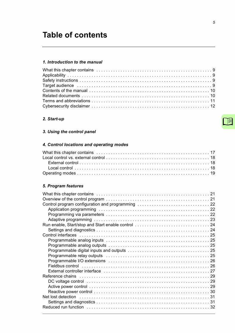
5
Table of contents
1. Introduction to the manual
What this chapter contains . . . . . . . . . . . . . . . . . . . . . . . . . . . . . . . . . . . . . . . . . . . . . . . . 9Applicability . . . . . . . . . . . . . . . . . . . . . . . . . . . . . . . . . . . . . . . . . . . . . . . . . . . . . . . . . . . . 9Safety instructions . . . . . . . . . . . . . . . . . . . . . . . . . . . . . . . . . . . . . . . . . . . . . . . . . . . . . . . 9Target audience . . . . . . . . . . . . . . . . . . . . . . . . . . . . . . . . . . . . . . . . . . . . . . . . . . . . . . . . 9Contents of the manual . . . . . . . . . . . . . . . . . . . . . . . . . . . . . . . . . . . . . . . . . . . . . . . . . . 10Related documents . . . . . . . . . . . . . . . . . . . . . . . . . . . . . . . . . . . . . . . . . . . . . . . . . . . . . 10Terms and abbreviations . . . . . . . . . . . . . . . . . . . . . . . . . . . . . . . . . . . . . . . . . . . . . . . . . 11Cybersecurity disclaimer . . . . . . . . . . . . . . . . . . . . . . . . . . . . . . . . . . . . . . . . . . . . . . . . . 12
2. Start-up
3. Using the control panel
4. Control locations and operating modes
What this chapter contains . . . . . . . . . . . . . . . . . . . . . . . . . . . . . . . . . . . . . . . . . . . . . . . 17Local control vs. external control . . . . . . . . . . . . . . . . . . . . . . . . . . . . . . . . . . . . . . . . . . . 18
External control . . . . . . . . . . . . . . . . . . . . . . . . . . . . . . . . . . . . . . . . . . . . . . . . . . . . . . 18Local control . . . . . . . . . . . . . . . . . . . . . . . . . . . . . . . . . . . . . . . . . . . . . . . . . . . . . . . . 18
Operating modes . . . . . . . . . . . . . . . . . . . . . . . . . . . . . . . . . . . . . . . . . . . . . . . . . . . . . . . 19
5. Program features
What this chapter contains . . . . . . . . . . . . . . . . . . . . . . . . . . . . . . . . . . . . . . . . . . . . . . . 21Overview of the control program . . . . . . . . . . . . . . . . . . . . . . . . . . . . . . . . . . . . . . . . . . . 21Control program configuration and programming . . . . . . . . . . . . . . . . . . . . . . . . . . . . . . 22
Application programming . . . . . . . . . . . . . . . . . . . . . . . . . . . . . . . . . . . . . . . . . . . . . . 22Programming via parameters . . . . . . . . . . . . . . . . . . . . . . . . . . . . . . . . . . . . . . . . . . . 22Adaptive programming . . . . . . . . . . . . . . . . . . . . . . . . . . . . . . . . . . . . . . . . . . . . . . . . 23
Run enable, Start/stop and Start enable control . . . . . . . . . . . . . . . . . . . . . . . . . . . . . . . 24Settings and diagnostics . . . . . . . . . . . . . . . . . . . . . . . . . . . . . . . . . . . . . . . . . . . . . . . 24
Control interfaces . . . . . . . . . . . . . . . . . . . . . . . . . . . . . . . . . . . . . . . . . . . . . . . . . . . . . . 25Programmable analog inputs . . . . . . . . . . . . . . . . . . . . . . . . . . . . . . . . . . . . . . . . . . . 25Programmable analog outputs . . . . . . . . . . . . . . . . . . . . . . . . . . . . . . . . . . . . . . . . . . 25Programmable digital inputs and outputs . . . . . . . . . . . . . . . . . . . . . . . . . . . . . . . . . . 25Programmable relay outputs . . . . . . . . . . . . . . . . . . . . . . . . . . . . . . . . . . . . . . . . . . . 25Programmable I/O extensions . . . . . . . . . . . . . . . . . . . . . . . . . . . . . . . . . . . . . . . . . . 26Fieldbus control . . . . . . . . . . . . . . . . . . . . . . . . . . . . . . . . . . . . . . . . . . . . . . . . . . . . . 26External controller interface . . . . . . . . . . . . . . . . . . . . . . . . . . . . . . . . . . . . . . . . . . . . 27
Reference chains . . . . . . . . . . . . . . . . . . . . . . . . . . . . . . . . . . . . . . . . . . . . . . . . . . . . . . 29DC voltage control . . . . . . . . . . . . . . . . . . . . . . . . . . . . . . . . . . . . . . . . . . . . . . . . . . . 29Active power control . . . . . . . . . . . . . . . . . . . . . . . . . . . . . . . . . . . . . . . . . . . . . . . . . . 29Reactive power control . . . . . . . . . . . . . . . . . . . . . . . . . . . . . . . . . . . . . . . . . . . . . . . . 30
Net lost detection . . . . . . . . . . . . . . . . . . . . . . . . . . . . . . . . . . . . . . . . . . . . . . . . . . . . . . 31Settings and diagnostics . . . . . . . . . . . . . . . . . . . . . . . . . . . . . . . . . . . . . . . . . . . . . . . 31
Reduced run function . . . . . . . . . . . . . . . . . . . . . . . . . . . . . . . . . . . . . . . . . . . . . . . . . . . 32
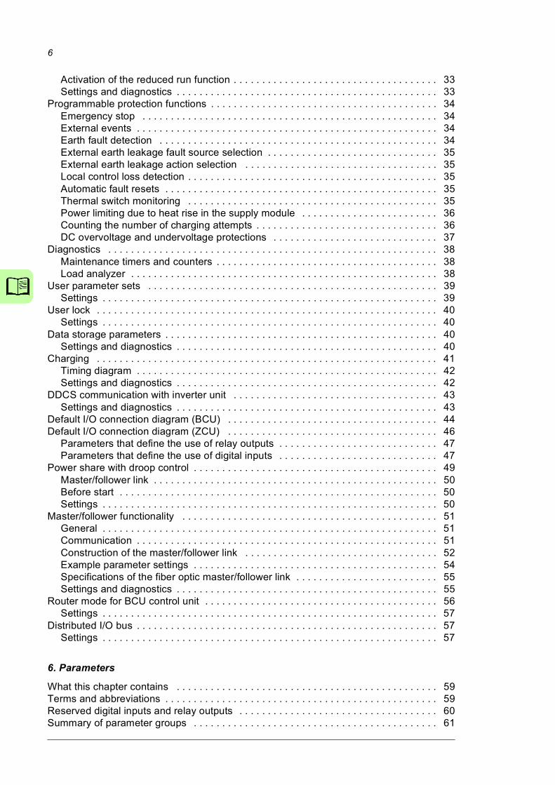
6
Activation of the reduced run function . . . . . . . . . . . . . . . . . . . . . . . . . . . . . . . . . . . . 33Settings and diagnostics . . . . . . . . . . . . . . . . . . . . . . . . . . . . . . . . . . . . . . . . . . . . . . 33
Programmable protection functions . . . . . . . . . . . . . . . . . . . . . . . . . . . . . . . . . . . . . . . . 34Emergency stop . . . . . . . . . . . . . . . . . . . . . . . . . . . . . . . . . . . . . . . . . . . . . . . . . . . . 34External events . . . . . . . . . . . . . . . . . . . . . . . . . . . . . . . . . . . . . . . . . . . . . . . . . . . . . 34Earth fault detection . . . . . . . . . . . . . . . . . . . . . . . . . . . . . . . . . . . . . . . . . . . . . . . . . 34External earth leakage fault source selection . . . . . . . . . . . . . . . . . . . . . . . . . . . . . . 35External earth leakage action selection . . . . . . . . . . . . . . . . . . . . . . . . . . . . . . . . . . 35Local control loss detection . . . . . . . . . . . . . . . . . . . . . . . . . . . . . . . . . . . . . . . . . . . . 35Automatic fault resets . . . . . . . . . . . . . . . . . . . . . . . . . . . . . . . . . . . . . . . . . . . . . . . . 35Thermal switch monitoring . . . . . . . . . . . . . . . . . . . . . . . . . . . . . . . . . . . . . . . . . . . . 35Power limiting due to heat rise in the supply module . . . . . . . . . . . . . . . . . . . . . . . . 36Counting the number of charging attempts . . . . . . . . . . . . . . . . . . . . . . . . . . . . . . . . 36DC overvoltage and undervoltage protections . . . . . . . . . . . . . . . . . . . . . . . . . . . . . 37
Diagnostics . . . . . . . . . . . . . . . . . . . . . . . . . . . . . . . . . . . . . . . . . . . . . . . . . . . . . . . . . . 38Maintenance timers and counters . . . . . . . . . . . . . . . . . . . . . . . . . . . . . . . . . . . . . . . 38Load analyzer . . . . . . . . . . . . . . . . . . . . . . . . . . . . . . . . . . . . . . . . . . . . . . . . . . . . . . 38
User parameter sets . . . . . . . . . . . . . . . . . . . . . . . . . . . . . . . . . . . . . . . . . . . . . . . . . . . 39Settings . . . . . . . . . . . . . . . . . . . . . . . . . . . . . . . . . . . . . . . . . . . . . . . . . . . . . . . . . . . 39
User lock . . . . . . . . . . . . . . . . . . . . . . . . . . . . . . . . . . . . . . . . . . . . . . . . . . . . . . . . . . . . 40Settings . . . . . . . . . . . . . . . . . . . . . . . . . . . . . . . . . . . . . . . . . . . . . . . . . . . . . . . . . . . 40
Data storage parameters . . . . . . . . . . . . . . . . . . . . . . . . . . . . . . . . . . . . . . . . . . . . . . . . 40Settings and diagnostics . . . . . . . . . . . . . . . . . . . . . . . . . . . . . . . . . . . . . . . . . . . . . . 40
Charging . . . . . . . . . . . . . . . . . . . . . . . . . . . . . . . . . . . . . . . . . . . . . . . . . . . . . . . . . . . . 41Timing diagram . . . . . . . . . . . . . . . . . . . . . . . . . . . . . . . . . . . . . . . . . . . . . . . . . . . . . 42Settings and diagnostics . . . . . . . . . . . . . . . . . . . . . . . . . . . . . . . . . . . . . . . . . . . . . . 42
DDCS communication with inverter unit . . . . . . . . . . . . . . . . . . . . . . . . . . . . . . . . . . . . 43Settings and diagnostics . . . . . . . . . . . . . . . . . . . . . . . . . . . . . . . . . . . . . . . . . . . . . . 43
Default I/O connection diagram (BCU) . . . . . . . . . . . . . . . . . . . . . . . . . . . . . . . . . . . . . 44Default I/O connection diagram (ZCU) . . . . . . . . . . . . . . . . . . . . . . . . . . . . . . . . . . . . . 46
Parameters that define the use of relay outputs . . . . . . . . . . . . . . . . . . . . . . . . . . . . 47Parameters that define the use of digital inputs . . . . . . . . . . . . . . . . . . . . . . . . . . . . 47
Power share with droop control . . . . . . . . . . . . . . . . . . . . . . . . . . . . . . . . . . . . . . . . . . . 49Master/follower link . . . . . . . . . . . . . . . . . . . . . . . . . . . . . . . . . . . . . . . . . . . . . . . . . . 50Before start . . . . . . . . . . . . . . . . . . . . . . . . . . . . . . . . . . . . . . . . . . . . . . . . . . . . . . . . 50Settings . . . . . . . . . . . . . . . . . . . . . . . . . . . . . . . . . . . . . . . . . . . . . . . . . . . . . . . . . . . 50
Master/follower functionality . . . . . . . . . . . . . . . . . . . . . . . . . . . . . . . . . . . . . . . . . . . . . 51General . . . . . . . . . . . . . . . . . . . . . . . . . . . . . . . . . . . . . . . . . . . . . . . . . . . . . . . . . . . 51Communication . . . . . . . . . . . . . . . . . . . . . . . . . . . . . . . . . . . . . . . . . . . . . . . . . . . . . 51Construction of the master/follower link . . . . . . . . . . . . . . . . . . . . . . . . . . . . . . . . . . 52Example parameter settings . . . . . . . . . . . . . . . . . . . . . . . . . . . . . . . . . . . . . . . . . . . 54Specifications of the fiber optic master/follower link . . . . . . . . . . . . . . . . . . . . . . . . . 55Settings and diagnostics . . . . . . . . . . . . . . . . . . . . . . . . . . . . . . . . . . . . . . . . . . . . . . 55
Router mode for BCU control unit . . . . . . . . . . . . . . . . . . . . . . . . . . . . . . . . . . . . . . . . . 56Settings . . . . . . . . . . . . . . . . . . . . . . . . . . . . . . . . . . . . . . . . . . . . . . . . . . . . . . . . . . . 57
Distributed I/O bus . . . . . . . . . . . . . . . . . . . . . . . . . . . . . . . . . . . . . . . . . . . . . . . . . . . . . 57Settings . . . . . . . . . . . . . . . . . . . . . . . . . . . . . . . . . . . . . . . . . . . . . . . . . . . . . . . . . . . 57
6. Parameters
What this chapter contains . . . . . . . . . . . . . . . . . . . . . . . . . . . . . . . . . . . . . . . . . . . . . . 59Terms and abbreviations . . . . . . . . . . . . . . . . . . . . . . . . . . . . . . . . . . . . . . . . . . . . . . . . 59Reserved digital inputs and relay outputs . . . . . . . . . . . . . . . . . . . . . . . . . . . . . . . . . . . 60Summary of parameter groups . . . . . . . . . . . . . . . . . . . . . . . . . . . . . . . . . . . . . . . . . . . 61

7
Parameter listing . . . . . . . . . . . . . . . . . . . . . . . . . . . . . . . . . . . . . . . . . . . . . . . . . . . . . . . 63101 Actual values . . . . . . . . . . . . . . . . . . . . . . . . . . . . . . . . . . . . . . . . . . . . . . . . . . . . 63103 Input references . . . . . . . . . . . . . . . . . . . . . . . . . . . . . . . . . . . . . . . . . . . . . . . . . . 65104 Warnings and faults . . . . . . . . . . . . . . . . . . . . . . . . . . . . . . . . . . . . . . . . . . . . . . . 66105 Diagnostics . . . . . . . . . . . . . . . . . . . . . . . . . . . . . . . . . . . . . . . . . . . . . . . . . . . . . 71106 Control and status words . . . . . . . . . . . . . . . . . . . . . . . . . . . . . . . . . . . . . . . . . . . 72107 System info . . . . . . . . . . . . . . . . . . . . . . . . . . . . . . . . . . . . . . . . . . . . . . . . . . . . . 78110 Standard DI, RO . . . . . . . . . . . . . . . . . . . . . . . . . . . . . . . . . . . . . . . . . . . . . . . . . 79111 Standard DIO, FI, FO . . . . . . . . . . . . . . . . . . . . . . . . . . . . . . . . . . . . . . . . . . . . . . 83112 Standard AI . . . . . . . . . . . . . . . . . . . . . . . . . . . . . . . . . . . . . . . . . . . . . . . . . . . . . 86113 Standard AO . . . . . . . . . . . . . . . . . . . . . . . . . . . . . . . . . . . . . . . . . . . . . . . . . . . . 89114 Extension I/O module 1 . . . . . . . . . . . . . . . . . . . . . . . . . . . . . . . . . . . . . . . . . . . . 92115 Extension I/O module 2 . . . . . . . . . . . . . . . . . . . . . . . . . . . . . . . . . . . . . . . . . . . 107116 Extension I/O module 3 . . . . . . . . . . . . . . . . . . . . . . . . . . . . . . . . . . . . . . . . . . . 111119 Operation mode . . . . . . . . . . . . . . . . . . . . . . . . . . . . . . . . . . . . . . . . . . . . . . . . . 114120 Start/stop . . . . . . . . . . . . . . . . . . . . . . . . . . . . . . . . . . . . . . . . . . . . . . . . . . . . . . 115121 Start/stop mode . . . . . . . . . . . . . . . . . . . . . . . . . . . . . . . . . . . . . . . . . . . . . . . . . 120122 Power reference . . . . . . . . . . . . . . . . . . . . . . . . . . . . . . . . . . . . . . . . . . . . . . . . 120123 DC voltage reference . . . . . . . . . . . . . . . . . . . . . . . . . . . . . . . . . . . . . . . . . . . . . 122124 Reactive power reference . . . . . . . . . . . . . . . . . . . . . . . . . . . . . . . . . . . . . . . . . 123130 Limits . . . . . . . . . . . . . . . . . . . . . . . . . . . . . . . . . . . . . . . . . . . . . . . . . . . . . . . . . 127131 Fault functions . . . . . . . . . . . . . . . . . . . . . . . . . . . . . . . . . . . . . . . . . . . . . . . . . . 131133 Generic timer & counter . . . . . . . . . . . . . . . . . . . . . . . . . . . . . . . . . . . . . . . . . . . 137136 Load analyzer . . . . . . . . . . . . . . . . . . . . . . . . . . . . . . . . . . . . . . . . . . . . . . . . . . 142146 Monitoring settings . . . . . . . . . . . . . . . . . . . . . . . . . . . . . . . . . . . . . . . . . . . . . . 145147 Data storage . . . . . . . . . . . . . . . . . . . . . . . . . . . . . . . . . . . . . . . . . . . . . . . . . . . 146149 Panel port communication . . . . . . . . . . . . . . . . . . . . . . . . . . . . . . . . . . . . . . . . . 148150 FBA . . . . . . . . . . . . . . . . . . . . . . . . . . . . . . . . . . . . . . . . . . . . . . . . . . . . . . . . . . 148151 FBA A settings . . . . . . . . . . . . . . . . . . . . . . . . . . . . . . . . . . . . . . . . . . . . . . . . . . 153152 FBA A data in . . . . . . . . . . . . . . . . . . . . . . . . . . . . . . . . . . . . . . . . . . . . . . . . . . . 154153 FBA A data out . . . . . . . . . . . . . . . . . . . . . . . . . . . . . . . . . . . . . . . . . . . . . . . . . . 155154 FBA B settings . . . . . . . . . . . . . . . . . . . . . . . . . . . . . . . . . . . . . . . . . . . . . . . . . . 155155 FBA B data in . . . . . . . . . . . . . . . . . . . . . . . . . . . . . . . . . . . . . . . . . . . . . . . . . . . 157156 FBA B data out . . . . . . . . . . . . . . . . . . . . . . . . . . . . . . . . . . . . . . . . . . . . . . . . . 157160 DDCS communication . . . . . . . . . . . . . . . . . . . . . . . . . . . . . . . . . . . . . . . . . . . . 158161 DDCS transmit . . . . . . . . . . . . . . . . . . . . . . . . . . . . . . . . . . . . . . . . . . . . . . . . . . 164162 DDCS receive . . . . . . . . . . . . . . . . . . . . . . . . . . . . . . . . . . . . . . . . . . . . . . . . . . 168190 BAMU measurements . . . . . . . . . . . . . . . . . . . . . . . . . . . . . . . . . . . . . . . . . . . . 175191 BAMU configuration . . . . . . . . . . . . . . . . . . . . . . . . . . . . . . . . . . . . . . . . . . . . . . 176195 HW configuration . . . . . . . . . . . . . . . . . . . . . . . . . . . . . . . . . . . . . . . . . . . . . . . . 177196 System . . . . . . . . . . . . . . . . . . . . . . . . . . . . . . . . . . . . . . . . . . . . . . . . . . . . . . . . 181199 Off grid configuration . . . . . . . . . . . . . . . . . . . . . . . . . . . . . . . . . . . . . . . . . . . . . 187206 I/O bus configuration . . . . . . . . . . . . . . . . . . . . . . . . . . . . . . . . . . . . . . . . . . . . . 187207 I/O bus service . . . . . . . . . . . . . . . . . . . . . . . . . . . . . . . . . . . . . . . . . . . . . . . . . . 187208 I/O bus diagnostics . . . . . . . . . . . . . . . . . . . . . . . . . . . . . . . . . . . . . . . . . . . . . . 187209 I/O bus fan identification . . . . . . . . . . . . . . . . . . . . . . . . . . . . . . . . . . . . . . . . . . 187
7. Additional parameter data
What this chapter contains . . . . . . . . . . . . . . . . . . . . . . . . . . . . . . . . . . . . . . . . . . . . . . 189Terms and abbreviations . . . . . . . . . . . . . . . . . . . . . . . . . . . . . . . . . . . . . . . . . . . . . . . . 189Fieldbus addresses . . . . . . . . . . . . . . . . . . . . . . . . . . . . . . . . . . . . . . . . . . . . . . . . . . . . 190Parameter groups 101…107 . . . . . . . . . . . . . . . . . . . . . . . . . . . . . . . . . . . . . . . . . . . . . 191Parameter groups 110…209 . . . . . . . . . . . . . . . . . . . . . . . . . . . . . . . . . . . . . . . . . . . . . 195

8
8. Fault tracing
What this chapter contains . . . . . . . . . . . . . . . . . . . . . . . . . . . . . . . . . . . . . . . . . . . . . 219Safety . . . . . . . . . . . . . . . . . . . . . . . . . . . . . . . . . . . . . . . . . . . . . . . . . . . . . . . . . . . . . . 219Indications . . . . . . . . . . . . . . . . . . . . . . . . . . . . . . . . . . . . . . . . . . . . . . . . . . . . . . . . . . 220
Warnings and faults . . . . . . . . . . . . . . . . . . . . . . . . . . . . . . . . . . . . . . . . . . . . . . . . 220Pure events . . . . . . . . . . . . . . . . . . . . . . . . . . . . . . . . . . . . . . . . . . . . . . . . . . . . . . . 220Editable messages . . . . . . . . . . . . . . . . . . . . . . . . . . . . . . . . . . . . . . . . . . . . . . . . . 220
Warning/fault history and analysis . . . . . . . . . . . . . . . . . . . . . . . . . . . . . . . . . . . . . . . . 220Event logs . . . . . . . . . . . . . . . . . . . . . . . . . . . . . . . . . . . . . . . . . . . . . . . . . . . . . . . . 220Other data loggers . . . . . . . . . . . . . . . . . . . . . . . . . . . . . . . . . . . . . . . . . . . . . . . . . 221Parameters that contain warning/fault information . . . . . . . . . . . . . . . . . . . . . . . . . 221
Fault and warning words . . . . . . . . . . . . . . . . . . . . . . . . . . . . . . . . . . . . . . . . . . . . . . . 222Warning messages . . . . . . . . . . . . . . . . . . . . . . . . . . . . . . . . . . . . . . . . . . . . . . . . . . . 224Fault messages . . . . . . . . . . . . . . . . . . . . . . . . . . . . . . . . . . . . . . . . . . . . . . . . . . . . . . 235
9. Fieldbus control through the embedded fieldbus interface (EFB)
10. Fieldbus control through a fieldbus adapter
What this chapter contains . . . . . . . . . . . . . . . . . . . . . . . . . . . . . . . . . . . . . . . . . . . . . 251System overview . . . . . . . . . . . . . . . . . . . . . . . . . . . . . . . . . . . . . . . . . . . . . . . . . . . . . 252Basics of the fieldbus control interface . . . . . . . . . . . . . . . . . . . . . . . . . . . . . . . . . . . . 253
Control word and Status word . . . . . . . . . . . . . . . . . . . . . . . . . . . . . . . . . . . . . . . . . 253References . . . . . . . . . . . . . . . . . . . . . . . . . . . . . . . . . . . . . . . . . . . . . . . . . . . . . . . 253Actual values . . . . . . . . . . . . . . . . . . . . . . . . . . . . . . . . . . . . . . . . . . . . . . . . . . . . . . 254Fieldbus scaling diagram . . . . . . . . . . . . . . . . . . . . . . . . . . . . . . . . . . . . . . . . . . . . 255Contents of the fieldbus Control word . . . . . . . . . . . . . . . . . . . . . . . . . . . . . . . . . . . 256Contents of the fieldbus Status word . . . . . . . . . . . . . . . . . . . . . . . . . . . . . . . . . . . 257The state diagram . . . . . . . . . . . . . . . . . . . . . . . . . . . . . . . . . . . . . . . . . . . . . . . . . . 258
Setting up the IGBT supply unit for fieldbus control . . . . . . . . . . . . . . . . . . . . . . . . . . . 259Setting up communication through inverter unit . . . . . . . . . . . . . . . . . . . . . . . . . . . . . 260
11. Drive-to-drive link
12. Control chain diagrams
What this chapter contains . . . . . . . . . . . . . . . . . . . . . . . . . . . . . . . . . . . . . . . . . . . . . 263DC voltage reference chain . . . . . . . . . . . . . . . . . . . . . . . . . . . . . . . . . . . . . . . . . . . . . 264Power reference chain . . . . . . . . . . . . . . . . . . . . . . . . . . . . . . . . . . . . . . . . . . . . . . . . . 265Reactive power reference chain . . . . . . . . . . . . . . . . . . . . . . . . . . . . . . . . . . . . . . . . . 266
Reactive power control overview . . . . . . . . . . . . . . . . . . . . . . . . . . . . . . . . . . . . . . 266Reactive power control detail – Processing of the reference type AC voltage . . . . 267
Current limitation chain . . . . . . . . . . . . . . . . . . . . . . . . . . . . . . . . . . . . . . . . . . . . . . . . 268
Further informationProduct and service inquiries . . . . . . . . . . . . . . . . . . . . . . . . . . . . . . . . . . . . . . . . . . . . 269Product training. . . . . . . . . . . . . . . . . . . . . . . . . . . . . . . . . . . . . . . . . . . . . . . . . . . . . . . 269Providing feedback on ABB Drives manuals . . . . . . . . . . . . . . . . . . . . . . . . . . . . . . . . 269Document library on the Internet . . . . . . . . . . . . . . . . . . . . . . . . . . . . . . . . . . . . . . . . . 269
Introduction to the manual 9
1
Introduction to the manual
What this chapter containsThis chapter describes the contents of the manual. It also contains information on the compatibility, safety and intended audience.
ApplicabilityThis manual applies to ACS880 IGBT supply control program (AISLX v3.0x or later) and ACS880 IGBT supply control program 2Q (ALHLX v3.0x or later) used in ACS880 drives. The manual covers two versions of the control program: IGBT supply control program for the regenerative drives, and IGBT supply control program for the ultra-low harmonic drives (non-regenerative). The regenerative drives are ACS880 multidrive with IGBT supply unit (ACS880-204, ACS880-204LC, ACS880-207, ACS880-207LC), ACS880-11, ACS880-14, ACS880-17 and ACS880-17LC. The ultra-low harmonic drives are ACS880-31, ACS880-34, ACS880-37 and ACS880-37LC.
Safety instructionsFollow all safety instructions delivered with the drive.• Read the complete safety instructions before you install, commission, or use the
drive. See ACS880 multidrive cabinets and modules safety instructions (3AUA0000102301 [English]).
• Read the firmware function-specific warnings and notes before changing parameter values. These warnings and notes are included in the parameter descriptions presented in chapter Parameters.
Target audienceThis manual is intended for people who design, commission, or operate the drive system.

10 Introduction to the manual
Contents of the manualThis manual consists of the following chapters:• Start-up refers to where the start-up procedure of the supply unit is described.
• Using the control panel provides the basic instructions for use of the control panel.
• Control locations and operating modes describes the control locations and operating modes supported by the control program.
• Program features describes the features and I/O interface of the control program.
• Parameters describes the parameters of the control program.
• Additional parameter data contains further information on the parameters.
• Fault tracing lists the warning and fault messages with possible causes and remedies.
• Fieldbus control through the embedded fieldbus interface (EFB) describes the communication to and from a fieldbus network using the embedded fieldbus interface.
• Fieldbus control through a fieldbus adapter describes the communication to and from a fieldbus network using an optional fieldbus adapter module.
• Drive-to-drive link describes the communication between drives connected together by the drive-to-drive (D2D) link.
• Control chain diagrams presents the control chain diagrams of the control program.
Related documentsA list of related manuals is printed on the inside of the front cover.

Introduction to the manual 11
Terms and abbreviationsTerm/abbreviation Definition
ACS-AP-I Types of control panel used with ACS880 drives
ACS-AP-W
AI Analog input; interface for analog input signals
AO Analog output; interface for analog output signals
BAMU Auxiliary measurement unit
BCU Type of control unit used in ACS880 drives.
BU Branching unit
Control board Circuit board in which the control program runs.
Control unit Control board built in a rail-mountable housing
DC link DC circuit between rectifier and inverter
DDCS Distributed drives communication system; a protocol used in optical fiber communication
DI Digital input; interface for digital input signals
DIO Digital input/output; interface that can be used as a digital input or output
DO Digital output; interface for digital output signals
EFB Embedded fieldbus
FAIO-01 Optional analog I/O extension module
FBA Fieldbus adapter
FIO-01 Optional digital I/O extension module
FIO-11 Optional analog I/O extension module
FCAN-0x Optional CANopen® adapter
FCNA-0x Optional ControlNet™ adapter
FDCO-0x Optional DDCS communication module
FDIO-01 Optional digital I/O extension module
FDNA-0x Optional DeviceNet™ adapter
FEA-03 Optional I/O extension adapter
FECA-01 Optional EtherCAT® adapter
FENA-11 Optional EtherNet/IP™, Modbus TCP® and PROFINET IO® adapter
FENA-21 Optional dual-port EtherNet/IP, Modbus TCP and PROFINET IO adapter
FEPL-0x Optional Ethernet POWERLINK adapter
FPBA-0x Optional PROFIBUS DP® adapter
FSCA-0x Optional Modbus® adapter
IGBT Insulated gate bipolar transistor; a voltage-controlled semiconductor type widely used in converters due to their easy controllability and high switching frequency
IGBT supply unit (ISU) IGBT supply module(s) under control of one control board, and related components such as LCL filters, main contactor, fuses etc.
Inverter unit (INU) Inverter module(s) under control of one control board, and related components. One inverter unit typically controls one motor.
I/O Input/Output
LCL filter Inductor-capacitor-inductor filter for attenuating harmonics
MCB Main circuit breaker. Electrically-controlled main switching and protecting device. A withdrawable breaker can also be used as the main disconnector.
MSW Main status word
Parameter User-adjustable operation instruction to the drive, or signal measured or calculated by the drive
PLC Programmable logic controller
RDCO-0x DDCS communication module
RO Relay output; interface for a digital output signal. Implemented with a relay.

12 Introduction to the manual
Cybersecurity disclaimerThis product is designed to be connected to and to communicate information and data via a network interface. It is Customer's sole responsibility to provide and continuously ensure a secure connection between the product and Customer network or any other network (as the case may be). Customer shall establish and maintain any appropriate measures (such as but not limited to the installation of firewalls, application of authentication measures, encryption of data, installation of anti-virus programs, etc) to protect the product, the network, its system and the interface against any kind of security breaches, unauthorized access, interference, intrusion, leakage and/or theft of data or information. ABB and its affiliates are not liable for damages and/or losses related to such security breaches, any unauthorized access, interference, intrusion, leakage and/or theft of data or information.
See also section User lock (page 40).
STO Safe torque off
ZCU Type of control unit used in ACS880 drives.
The control unit may be fitted onto the power module, or installed separately.
Term/abbreviation Definition
Start-up 13
2
Start-up
See the appropriate hardware manual. See List of related manuals on page 2.

14 Start-up
Using the control panel 15
3
Using the control panel
See ACX-AP-x assistant control panels user’s manual (3AUA0000085685 [English]).

16 Using the control panel
Control locations and operating modes 17
4
Control locations and operating modes
What this chapter containsThis chapter describes the control locations and operating modes supported by the control program.

18 Control locations and operating modes
Local control vs. external controlThe ACS880 has two main control locations: external and local. The control location is selected with the Loc/Rem key on the control panel or in the PC tool.
External control
When the supply unit is in external control, control commands are given through• the I/O terminals (digital and analog inputs), or optional I/O extension modules
• the embedded fieldbus interface or an optional fieldbus adapter module
• the external (DDCS) controller interface, and/or
• the drive-to-drive link.
External references are given through the fieldbus interface, analog inputs or drive-to-drive link.
Two external control locations, EXT1 and EXT2, are available. The user can select control signals (e.g. start and stop) and control modes for both external control locations. Depending on the user selection, either EXT1 or EXT2 is active at a time. Selection between EXT1/EXT2 is done via any binary source such as a digital input or fieldbus control word (see parameter 119.11 Ext1/Ext2 selection).
Note: Typically, ABB wires essential external control signals and status monitoring signals of a supply unit of the cabinet-installed drive to its digital inputs and relay outputs at the factory. We also set the parameters related to the external control signals accordingly. The commission engineer must not change these settings or the external control does not operate as planned. See the delivery-specific circuit diagrams.
Local control
The control commands are given from the control panel keypad or from a PC equipped with Drive composer when the supply unit is in local control.
Local control is mainly used during commissioning and maintenance. The control panel always overrides the external control signal sources when used in local control. When switched to local control, the control panel Start and Stop keys override the external Start/Stop source defined for the control program. However, to control the supply unit on
Control panel or Drive composer PC tool (optional)
Fieldbus adapter (Fxxx) or DDCS communication module
1) Extra inputs/outputs can be added by installing optional I/O extension modules (FIO-xx) in the option slots of the control unit.
PLC (= Programmable logic controller)
I/O 1)
Drive-to-drive (D2D) link or Embedded fieldbus interface
External control
Local control
ACS880

Control locations and operating modes 19
and off by the panel, you must still have the external Run enable and Start enable signals switched on at the appropriate digital inputs of the supply unit. See section Run enable, Start/stop and Start enable control on page 24. Changing the control location to local can be disabled by parameter 119.17 Local control disable.
The user can select by a parameter (149.05 Communication loss action) how the supply unit reacts to a control panel loss or PC tool communication break.
Operating modesThe IGBT supply unit can operate in three operating modes with different types of reference: • DC control
• power control
• AC voltage control (option +N8053).
In DC control and power control modes, the reactive power reference is possible simultaneously. The mode is selectable for each control location (Local, EXT1 and EXT2) in parameter group 119 Operation mode. For control chain diagrams of the DC control and power control modes, see chapter Control chain diagrams. For further information and control chain diagram of the AC voltage control mode, see Optimal grid control of ACS880 IGBT supply control program supplement (3AXD50000164745 [English]).

20 Control locations and operating modes

Program features 21
5
Program features
What this chapter containsThis chapter describes the features and I/O interface of the control program.
Overview of the control programACS880 IGBT supply control program controls the IGBT supply unit with an IGBT bridge type supply module. The main functions of the control program are:• maintain DC or active power reference,
• maintain reactive power reference,
• control external charging circuit (when used),
• control main contactor.
In addition, the control program protects the unit against overtemperature, DC or AC overvoltage and DC undervoltage. See section Charging on page 41. The control program also limits the active and reactive power as a function of the external temperature, and the temperature of the IGBTs. See section Power limiting due to heat rise in the supply module on page 36.
22 Program features
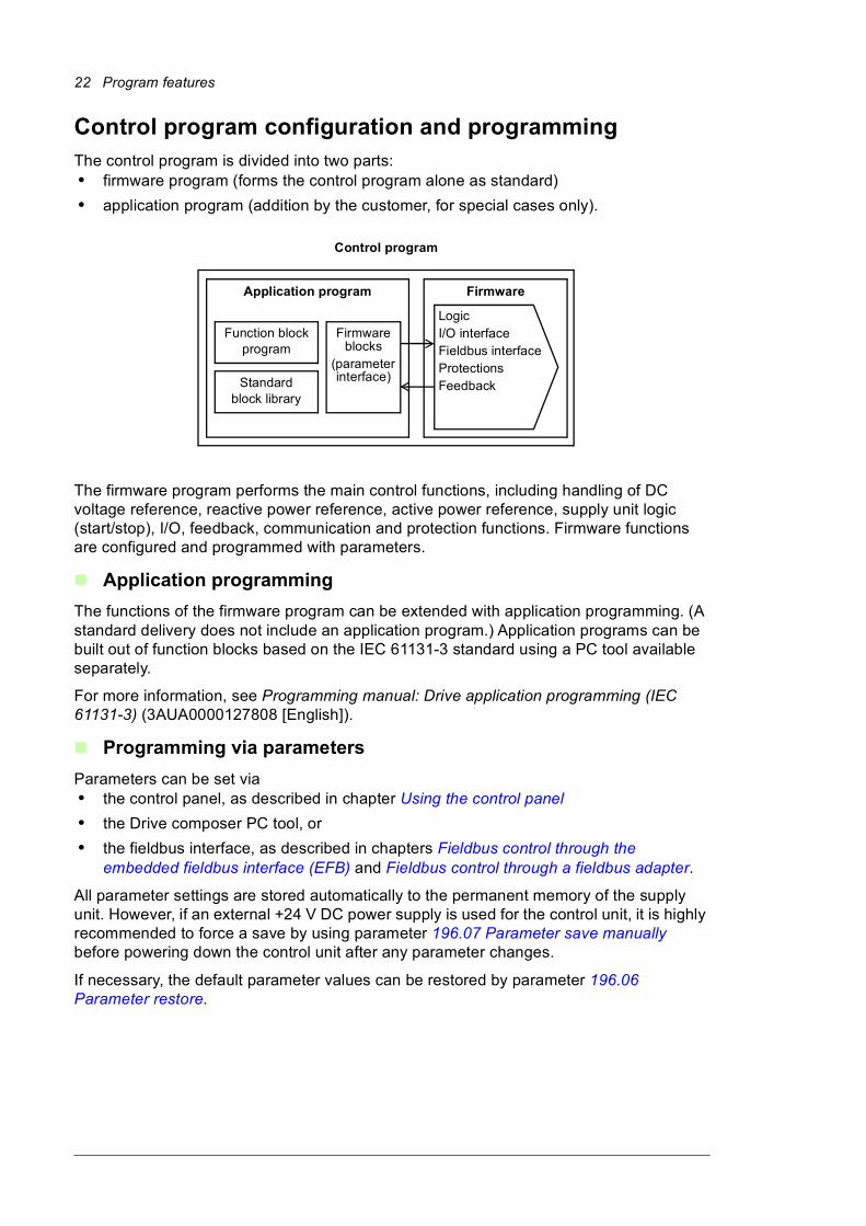
Control program configuration and programming The control program is divided into two parts: • firmware program (forms the control program alone as standard)
• application program (addition by the customer, for special cases only).
The firmware program performs the main control functions, including handling of DC voltage reference, reactive power reference, active power reference, supply unit logic (start/stop), I/O, feedback, communication and protection functions. Firmware functions are configured and programmed with parameters.
Application programming
The functions of the firmware program can be extended with application programming. (A standard delivery does not include an application program.) Application programs can be built out of function blocks based on the IEC 61131-3 standard using a PC tool available separately.
For more information, see Programming manual: Drive application programming (IEC 61131-3) (3AUA0000127808 [English]).
Programming via parameters
Parameters can be set via• the control panel, as described in chapter Using the control panel
• the Drive composer PC tool, or
• the fieldbus interface, as described in chapters Fieldbus control through the embedded fieldbus interface (EFB) and Fieldbus control through a fieldbus adapter.
All parameter settings are stored automatically to the permanent memory of the supply unit. However, if an external +24 V DC power supply is used for the control unit, it is highly recommended to force a save by using parameter 196.07 Parameter save manually before powering down the control unit after any parameter changes.
If necessary, the default parameter values can be restored by parameter 196.06 Parameter restore.
Application program Firmware
LogicI/O interfaceFieldbus interfaceProtectionsFeedbackStandard
block library
Function block program
Control program
Firmware blocks
(parameter interface)

Program features 23
Adaptive programming
Conventionally, the user can control the operation of the supply unit by parameters. However, the standard parameters have a fixed set of choices or a setting range. To further customize the operation of the supply unit, an adaptive program can be constructed out of a set of function blocks.
The Drive composer PC tool has an Adaptive programming feature with a graphical user interface for building the custom program. The function blocks include the usual arithmetic and logical functions, as well as eg. selection, comparison and timer blocks. The program can contain a maximum of 20 blocks. The adaptive program is executed on a 10 ms time level.
For selecting input to the program, the user interface has pre-selections for the physical inputs, common actual values, and other status information of the supply unit. Parameter values as well as constants can also be defined as inputs. The output of the program can be used eg. as a start signal, external event or reference, or connected to the drive outputs. Note that connecting the output of the adaptive program to a selection parameter will write-protect the parameter.
The status of the adaptive program is shown by parameter 107.30 Adaptive program status. The adaptive program can be disabled by 196.70 Disable adaptive program.
Please note that sequential programming is not supported.
For more information, see the Adaptive programming application guide (3AXD50000028574 [English]).
24 Program features
Run enable, Start/stop and Start enable controlThe user controls the operation of the IGBT supply unit with the Run enable command, Start/Stop command and Start enable command. When all commands are on in the control program, it controls the main contactor of the supply unit on with a relay output (relay output RO3 by default), and the charging contactor/relay (relay output RO1 by default). The main contactor connects the supply unit to the power line and the supply unit starts rectifying. If the Start/stop command or the Run enable command is off, the control program de-energizes the relay output and the main contactor switches off.
Note: If all supply and inverter modules connected to the common DC link have internal charging circuits of their own, no common charging circuit in the supply unit is needed, and the supply unit can start without doing the charging first. For more information, see section Charging on page 41. If any of the commands is off, the control program de-energizes the relay output and the main contactor switches off.
There is a parameter in the control program for defining the value or source for each of the commands. By default, the parameters define the command values or sources as follows:• Control program reads the Run enable command from digital input DI2.
• Control program reads the Start/Stop command from digital input DI2.
• Start enable is set on constantly.
Typically, DI2 is connected to the operating switch installed on the cabinet door. When the switch is on, the control program receives both the Run enable and Start/Stop commands via DI2.
Note: When you switch the control panel to local control, the control program starts reading the Start/Stop from the panel (Start and Stop keys). The parameter-defined Start/Stop source is not valid until you switch the panel back to remote control. The Loc/Rem key of the panel selects between local and remote control.
Note: Despite of the Local/Remote mode selection by the panel, the program reads the Run enable and Start enable from the interface defined by the appropriate parameters.
Note: Do not change the parameter settings related to Run enable, Start/Stop or Start enable unless you are absolutely sure what you are doing. The parameters settings and I/O wirings of the cabinet-installed unit are done at the factory according to the application requirements.
Settings and diagnostics
Control panel key: Loc/Rem
Parameters: parameter group 119 Operation mode, 120.01 Ext1 commands…120.09 Ext2 in2 source, 120.12 Run enable 1 source, 120.19 Enable start command
Warnings: AE5A Enable start signal missing, AE5B Run enable missing
Faults: 5E06 Main contactor Fault, 3E08 LSU charging
Program features 25
Control interfaces
Programmable analog inputs
The control unit has two programmable analog inputs. Each of the inputs can be independently set as a voltage (0/2…10 V or -10…10 V) or current (0/4…20 mA) input by a jumper or switch on the control unit. Each input can be filtered, inverted and scaled. The number of analog inputs can be increased by using FIO-11 or FAIO-01 I/O extensions.
Settings and diagnostics
Parameters: parameter group 112 Standard AI
Warnings: AE27 AI parameterization
Programmable analog outputs
The control unit has two current (0…20 mA) analog outputs. Each output can be filtered, inverted and scaled. The number of analog outputs can be increased by using FIO-11 or FAIO-01 I/O extensions.
Settings and diagnostics
Parameters: parameter group 113 Standard AO
Programmable digital inputs and outputs
The control unit has six digital inputs, a digital start interlock input, and two digital input/outputs.
Digital input/output DIO1 can be used as a frequency input, DIO2 as a frequency output.
The number of digital inputs/outputs can be increased by installing FIO-01, FIO-11 or FDIO-01 I/O extensions (see Programmable I/O extensions below).
Note: Do not change the settings of the reserved digital inputs (or outputs, if any). See subsection Reserved digital inputs and relay outputs on page 60.
Settings and diagnostics
Parameters: parameter groups 110 Standard DI, RO and 111 Standard DIO, FI, FO
Programmable relay outputs
The control unit has three relay outputs. The signal to be indicated by the outputs can be selected by parameters. Relay outputs can be added by installing FIO-01 or FDIO-01 I/O extensions.
Note: Do not change the settings of the reserved relay outputs. See subsection Reserved digital inputs and relay outputs on page 60.
Settings and diagnostics
Parameters: parameter group 110 Standard DI, RO

26 Program features
Programmable I/O extensions
The number of inputs and outputs can be increased by using I/O extension modules. The I/O configuration parameters include the maximum number of DI, DIO, AI, AO and RO that can be in use with different I/O extension module combinations. Slots can be added by connecting an FEA-03 I/O extension adapter.
The table below shows the possible I/O combinations:
Note: Not all the FIO-xx I/O extensions are supported by the current firmware version. (FIO-11 is supported.)
Settings and diagnostics
Parameters: parameter groups 110 Standard DI, RO, 111 Standard DIO, FI, FO,112 Standard AI, 113 Standard AO, 114 Extension I/O module 1,115 Extension I/O module 2, 116 Extension I/O module 3
Warnings: AE2E Extension AI parameterization, AE2F Extension I/O configuration failure
Faults: 7E00 Option module comm loss
Fieldbus control
The supply unit can be connected to an overriding control system via an optional fieldbus adapter. See chapter Fieldbus control through a fieldbus adapter (page 251).
Settings and diagnostics
Parameters: parameter groups 150 FBA, 151 FBA A settings, 152 FBA A data in, 153 FBA A data out, 154 FBA B settings, 155 FBA B data in, 156 FBA B data out
Warnings: AE25 FBA A parameter conflict, AE26 FBA B parameter conflict, AE30 FBA A communication, AE31 FBA B communication
Faults: 6E01 FBA A mapping file, 6E02 FBA B mapping file, 6E0D FBA A parameter conflict, 6E0E FBA B parameter conflict, 7E0B FBA A communication, 7E0C FBA B communication
LocationDigital inputs
(DI)
Digital I/Os
(DIO)
Analog inputs
(AI)
Analog outputs
(AO)
Relay outputs
(RO)
Control unit 7 2 2 2 3
FIO-01 - 4 - - 2
FIO-11 - 2 3 1 -
FAIO-01 - - 2 2 -
FDIO-01 3 - - - 2

Program features 27
External controller interface
General
The IGBT supply unit can be connected to an external controller (such as the ABB AC 800M) using either fiber optic or twisted-pair cable. The ACS880 is compatible with both the ModuleBus and DriveBus connections. Note that some features of DriveBus (such as BusManager) are not supported.
Topology
An example connection with either a ZCU-based or BCU-based IGBT supply unit using fiber optic cables is shown below.
IGBT supply units with a ZCU control unit require an additional FDCO DDCS communication module; IGBT supply units with a BCU control unit require an RDCO or FDCO module. The BCU has a dedicated slot for the RDCO – an FDCO module can also be used with a BCU control unit but it will reserve one of the three universal option module slots. Ring and star configurations are also possible much in the same way as with the master/follower link; the notable difference is that the external controller connects to channel CH0 on the RDCO module instead of CH2. The channel on the FDCO communication module can be freely selected.
Communication
The communication between the controller and the IGBT supply unit consists of data sets of three 16-bit words each. The controller sends a data set to the IGBT supply unit, which returns the next data set to the controller.
The communication uses data sets 10…33. The contents of the data sets are freely configurable, but data set 10 typically contains the control word, while data set 11 returns the status word and selected actual values.
The word that is defined as the control word is internally connected to the logic; the coding of the bits is as presented in section Contents of the fieldbus Control word (page 256). Likewise, the coding of the status word is as shown in section Contents of the fieldbus Status word (page 257).
T = Transmitter; R = Receiver
ACS880
(BCU) Control unit
RDCO
CH0
Controller
RT RT
ACS880
(ZCU) Control unit
FDCO
RT

28 Program features
By default, data sets 32 and 33 are dedicated for the mailbox service, which enables the setting or inquiry of parameter values as follows:
By parameter 160.64 Mailbox dataset selection, data sets 24 and 25 can be selected instead of data sets 32 and 33.
The update intervals of the data sets are as follows:• Data sets 10…11: 2 ms
• Data sets 12…13: 4 ms
• Data sets 14…17: 10 ms
• Data sets 18…25, 32, 33: 100 ms.
Settings
Parameter groups 160 DDCS communication (page 158), 161 DDCS transmit (page 164) and 162 DDCS receive (page 168).
�
� � � � � � �
�
� � � � � � �
�
� � � � � � �
�
� � � � � � �
�
� � � � � � �
�
� � � � � � �
� � � � � � � �
�
� � � � � � �
�
�
�
�
�
�
�
�
�
�
�
�
Data set
Data set
Data set
Data set
Data set
Data set
Par. Value
Parameter write to ISU
Parameter read from ISU
Transmit addressValue = 37653*Transmit dataValue = 1234Transmit addressfeedbackValue = 37653*
Inquire addressValue = 37654**Inquired dataValue = 4300Inquire addressfeedbackValue = 37654**
Controller ACS880
*147.21 -> 93h.15h -> 9315h -> 37653
**147.22 -> 93h.16h -> 9316h -> 37654
147.21
147.22
Program features 29
Reference chainsReference chains of the control program are• DC voltage reference chain,
• active power reference chain, and
• reactive power reference chain.
Tasks of the reference chains are reference source and type selection, limitation and ramping. The active power, DC voltage and reactive power reference chains are controlled by reference chain control. All of the reference chains are controlled by the bits of limit word (130.01).
DC voltage control
DC voltage is controlled by the DC voltage reference chain. DC voltage control is the default control mode of the supply unit. It is also the alternative control mode for the active power control. DC voltage control includes DC voltage reference selection, limitation and ramping. Incoming DC reference is limited between maximum and minimum of the DC limits. If the incoming reference exceeds the defined limits, the limit word is updated. DC reference is ramped according to DC ramp up and DC ramp down times.
Control chain diagram
See page 264.
Internal DC voltage reference
Lowest possible DC voltage level in IGBT supply unit is defined by AC voltage level. If DC voltage reference is lower than what the IGBT supply unit can achieve with control, reference is limited internally to the lowest possible value. Minimum DC voltage reference is filtered with 10 second time constant to prevent immediate drop in DC voltage reference while AC voltage level drops. See also the table on page 49.
Settings and diagnostics
Parameters: parameter groups 123 DC voltage reference and 130 Limits
Active power control
Active power is controlled by the power reference chain. Active power control is an alternative main control mode for the IGBT supply unit with the DC voltage control (which is the default control mode of the supply unit). Power reference chain includes reference selection, limitation and ramping.
The power reference modifies the input reference to active current reference for the ramp function. Possible input reference types are:• Active current reference in Amperes
• Active current reference in percent of the nominal current
• Power reference in kW
• Power reference in percent of the nominal power.
Main tasks of active current ramping are:• Active current reference limitation
• Active current reference ramping.
The control program contains a limitation feature for limiting the active power based on ambient temperature or the temperature of the IGBTs. The user can tune the limitation parameters.

30 Program features
Control chain diagram
See page 265.
Settings and diagnostics
Parameters: parameter groups 122 Power reference and 130 Limits
Reactive power control
Reactive power is controlled by the reactive power reference chain. Primarily, active power is controlled, and if there is reserve for reactive power, it can be controlled according to its reference. If a request for reactive power cannot be met, the control program indicates it with following parameters:• 130.03 Limit word 3
• bit 5 (Reactive current limit)
• bit 13 (Q act pos) *
• bit 14 (Q act neg) *
• 106.17 Drive status word 2
• bit 7 (Internal reactive power reference)
• 130.02 Limit word 2
• bit 0 (Q user ref max)
• bit 1 (Q user ref min)
* According to the polarity: positive = capacitive, negative = inductive.
If the IGBT supply unit is at its current limit, reactive power is limited before active power. Reactive power reference chain includes reference selection, limitation and ramping.
The reactive power reference modifies the input reference to reactive current reference. Possible input reference types are:• Reactive current reference in Amperes
• Reactive current reference in percent of the nominal current
• Reactive power reference in kVAr
• Reactive power reference in percent of the nominal power
• Reactive power reference angle in degrees
• Reactive power reference in cosphi
• Voltage reference for the AC voltage control in Volts
• Voltage reference for the AC voltage control in percent.
The type of the reactive power reference is selected with parameter.
Main tasks of the reactive current ramping are:• Reactive current reference limitation
• Reactive current reference ramping
• Ramp bypass in case of AC voltage control.
In reactive current reference limiting the incoming reference is limited between maximum and minimum of the reactive current limits. If the incoming reference exceeds the defined limits, the limit word is updated. The limited output is the input signal for the ramping function.
Program features 31
The control program also contains a limitation feature for limiting the reactive power based on ambient temperature or the temperature of the IGBTs. The user can tune the limitation parameters.
Control chain diagram
See page 266.
Settings and diagnostics
Parameters: parameter groups 124 Reactive power reference and 130 Limits
Net lost detectionThe IGBT supply unit recognizes the loss of supply AC voltage and recovers automatically when the AC voltage is connected again. The supply AC lost detection is based on fast (about 0.2 s, 10 Hz) change of the grid frequency estimate. When the frequency goes outside the frequency limits (+10 Hz of the nominal frequency), the control program activates the net lost state and generates a warning (AE78 Net lost). When the net lost is detected, there are two options: netlost
• If the grid voltage measurements are available, the IGBT supply unit tries to resynchronize to the grid when the grid voltages are connected again, and the frequency has been estimated to be between allowed limits. If the maximum duration of the net lost is exceeded (default 5 s), the IGBT supply unit trips to a fault (8E07 Net lost).
• If the measurements are not available, the IGBT supply unit tries to resynchronize to the grid at regular time intervals (default 0.1 s). If the resynchronization is not successful and the net lost lasts too long (default 5 s), the IGBT supply unit trips to a fault (8E07 Net lost).
Settings and diagnostics
Warnings: AE78 Net lost
Faults: 3E05 DC link undervoltage, 8E07 Net lost
32 Program features
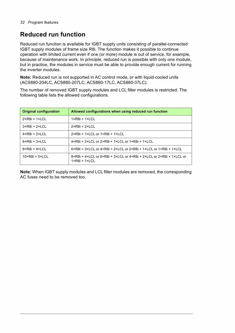
Reduced run function
Reduced run function is available for IGBT supply units consisting of parallel-connected IGBT supply modules of frame size R8i. The function makes it possible to continue operation with limited current even if one (or more) module is out of service, for example, because of maintenance work. In principle, reduced run is possible with only one module, but in practice, the modules in service must be able to provide enough current for running the inverter modules.
Note: Reduced run is not supported in AC control mode, or with liquid-cooled units (ACS880-204LC, ACS880-207LC, ACS880-17LC, ACS880-37LC).
The number of removed IGBT supply modules and LCL filter modules is restricted. The following table lists the allowed configurations.
Note: When IGBT supply modules and LCL filter modules are removed, the corresponding AC fuses need to be removed too.
Original configuration Allowed configurations when using reduced run function
2×R8i + 1×LCL 1×R8i + 1×LCL
3×R8i + 2×LCL 2×R8i + 2×LCL
4×R8i + 2×LCL 2×R8i + 1×LCL or 1×R8i + 1×LCL
6×R8i + 3×LCL 4×R8i + 2×LCL or 2×R8i + 1×LCL or 1×R8i + 1×LCL
8×R8i + 4×LCL 6×R8i + 3×LCL or 4×R8i + 2×LCL or 2×R8i + 1×LCL or 1×R8i + 1×LCL
10×R8i + 5×LCL 8×R8i + 4×LCL or 6×R8i + 3×LCL or 4×R8i + 2×LCL or 2×R8i + 1×LCL or 1×R8i + 1×LCL

Program features 33
Activation of the reduced run function
Note: For cabinet-built drives, the wiring accessories and the air baffle needed during the procedure are available from ABB, and are included in the delivery.
WARNING! Follow the safety instructions provided for the IGBT supply unit in question.
1. Disconnect the supply voltage and all other sources that can supply the DC bus (eg. DC/DC converter) from the IGBT supply unit.
2. If the control unit of the IGBT supply unit is powered from the faulty module, install an extension to the wiring and connect it to one of the remaining modules.
3. Remove the module to be serviced from its bay. See the appropriate hardware manual for instructions.
4. Install an air baffle to the top module guide to block the airflow through the empty module bay.
5. Switch on the power to the IGBT supply unit.
6. Enter the number of IGBT supply modules present into parameter 195.13 Reduced run mode.
7. Reset all faults and start the IGBT supply unit. The maximum current is now automatically limited according to the new configuration. A mismatch between the number of detected modules and the value set in 195.13 will generate a fault (5E0E Reduced run).
After all modules have been reinstalled, parameter 195.13 Reduced run mode must be reset to 0 to disable the reduced run function.
Settings and diagnostics
Parameters: 195.13 Reduced run mode, 195.14 Connected modules
Faults: 5E0E Reduced run

34 Program features
Programmable protection functions
Emergency stop
The emergency stop signal is connected to the input selected by parameter 121.05 Emergency stop source. An emergency stop can also be generated through fieldbus (parameter 106.01 Main control word, bits 1…2).
The way the IGBT supply unit is stopped when an emergency stop command is received, is selected with parameter 121.04 Emergency stop mode. The following selections are available:• stop and warning,
• warning,
• fault.
Notes:• The installer of the equipment is responsible for installing the emergency stop devices
and all additional devices needed for the emergency stop function to fulfill the required emergency stop categories. For more information, contact your local ABB representative.
• After an emergency stop signal is detected, the emergency stop function cannot be canceled even though the signal is canceled.
Settings and diagnostics
Parameters: 121.04 Emergency stop mode, 121.05 Emergency stop source
Warnings: AE68 Emergency stop warning
Faults: 6E1C Emergency stop fault
External events
An external event signal can be connected to a selectable input which is not used for other purposes. When the signal is lost, an external event (fault, warning, or a mere log entry) is generated.
Settings and diagnostics
Parameters: 131.01 External event 1 source…131.10 External event 5 type
Warnings: AE51 External warning 1…AE55 External warning 5
Faults: 9E01 External fault 1…9E05 External fault 5
Earth fault detection
The earth fault detection function is based on sum current measurement. Note that• in a grounded supply, the protection activates in 200 ms,
• in an ungrounded supply, the supply network capacitance should be 1 μF or more,
• the protection is deactivated when the supply unit is stopped.
Settings and diagnostics
Parameters: 131.20 Earth fault
Warnings: AE02 Earth leakage
Faults: 2E01 Earth leakage
Program features 35
External earth leakage fault source selection
The parameter selects in which digital input or digital input/output external earth leakage fault is connected.
Parameters: 131.28 Ext earth leakage signal source
Faults: 2E08 External earth fault
External earth leakage action selection
The parameter selects how the IGBT supply unit reacts when an external earth leakage is detected.
Parameters: 131.29 Ext earth leakage action
Faults: 2E08 External earth fault
Warnings: AE87 Ext earth leakage
Local control loss detection
The parameter selects how the supply unit reacts to a control panel or PC tool communication break.
Settings and diagnostics
Parameters: 149.05 Communication loss action
Faults: 7E01 Panel loss
Automatic fault resets
The supply unit can automatically reset itself after overcurrent, DC overvoltage, DC undervoltage, and external faults. The user can also specify a fault that is automatically reset.
By default, automatic resets are off and must be specifically activated by the user.
Settings and diagnostics
Parameters: 131.12 Autoreset selection…131.16 Delay time
Warnings: AE57 Autoreset
Thermal switch monitoring
The control program has a thermal switch monitoring function. The function monitors the status of the switch through a digital input typically. By default, digital input DI1 is used for monitoring the status of the thermal switch. Multiple switches must be connected in series. The commissioning engineer can activate the function and define the monitored input by a parameter. If the function receives an overtemperature indication (DI1 = 0), it trips the supply unit to a fault.
Settings and diagnostics
Parameters: 131.33 Cabinet temperature fault source, 131.34 Cabinet temperature supervision
Faults: 4E06 Cabinet or LCL overtemperature

36 Program features
Power limiting due to heat rise in the supply module
The control program has a supply module temperature monitoring function. The commissioning engineer can define:• the source for the coolant temperature measurement
• active and reactive power profile vs. temperature value
• warning and fault trip limits.
The function monitors the temperature of the coolant exiting the module. When the value reaches the limit defined for the power limiting profile, the control program starts limiting the power. If the temperature keeps rising despite of the power limiting, the control program generates first a warning (at warning limit), and then trips to a fault (at fault limit). User can activate and tune limitation in parameter group 130 Limits.
Example
Set parameter 130.50 Ext Tmp1 input selection with selection Other to 114.26 AI1 actual value. Set parameter 114.77 AO1 source with selection Other to 130.54 Pt current. It is possible to use groups 115 or 116 also.
Settings and diagnostics
Parameter groups: 130 Limits, 114 Extension I/O module 1…116 Extension I/O module 3
Warnings: AE10 Ext Tmp1 warning, AE11 Ext Tmp2 warning
Counting the number of charging attempts
The control program monitors charging attempts to prevent charging circuit overheating.
Settings and diagnostics
Parameters: 120.50 Charging overload event sel
Warnings: AE85 Charging count
Faults: 3E09 Charging count

Program features 37
DC overvoltage and undervoltage protections
The control program defines the DC overvoltage and undervoltage limits on basis of the supply voltage range given by the user with a parameter (195.01). The program monitors the actual voltage level with an internal voltage measurement. When the measured value exceeds the overvoltage limit or falls below the undervoltage limit, the control program trips to a fault.
Trip limits
The trip limits of the intermediate DC link voltage are relative to the supply voltage range selected with parameter 195.01 Supply voltage as well as supply unit type. The DC voltage is displayed by parameter 101.01 DC voltage. The following table shows the values of selected DC voltage levels in Volts.
Boost limits
Boost limit depends on the maximum voltage of the power module. Boost limits for DC voltage are given in the table below.
1) The control program limits the minimum value to sqrt(2) × Uac × (1.03…1.08).
2) The maximum value is limited by parameter 123.06 DC voltage ref max.
Settings and diagnostics
Parameters: 101.01 DC voltage, 123.06 DC voltage ref max, 195.01 Supply voltage
Warnings: AE09 DC link overvoltage, AE0A DC link undervoltage
Faults: 3E04 DC link overvoltage, 3E05 DC link undervoltage
Fault limit typeSupply voltage range (195.01)
380…415 V 440…480 V 500 V 525…600 V 660…690 V
Overvoltage fault limit (R1i…R6i, xxxxA-3)
844 - - - -
Overvoltage fault limit (R1i…R6i, xxxxA-5)
880 880 880 - -
Overvoltage fault limit (R8i, xxxxA-3) 859.5 - - - -
Overvoltage fault limit (R8i, xxxxA-5) 859.5 895.5 895.5 - -
Overvoltage fault limit (R8i, xxxxA-7) - - - 1293 1293
Undervoltage fault limit (all types) 308 357 405 425 535
IGBT supply module type
DC voltage reference range
Minimum[V]
Maximum[V]
xxxxA-3 1) 663 2)
xxxxA-5 1) 799 2)
xxxxA-7 1) 1102 2)
38 Program features
Diagnostics
Maintenance timers and counters
The program has six different maintenance timers or counters that can be configured to generate a warning when a pre-defined limit is reached. The contents of the message can be edited on the control panel by selecting Settings - Edit texts.
The timer/counter can be set to monitor any parameter. This feature is especially useful as a service reminder.
There are three types of counters:• On-time timers. Measures the time a binary source (for example, a bit in a status
word) is on.
• Signal edge counters. The counter is incremented whenever the monitored binary source changes state.
• Value counters. The counter measures, by integration, the monitored parameter. A warning is given when the calculated area below the signal exceeds a user-defined limit.
Settings and diagnostics
Parameters: parameter group 133 Generic timer & counter
Load analyzer
Peak value logger
The user can select a signal to be monitored by a peak value logger. The logger records the peak value of the signal along with the time the peak occurred, as well as supply unit current, DC voltage and power at the time of the peak.
Amplitude loggers
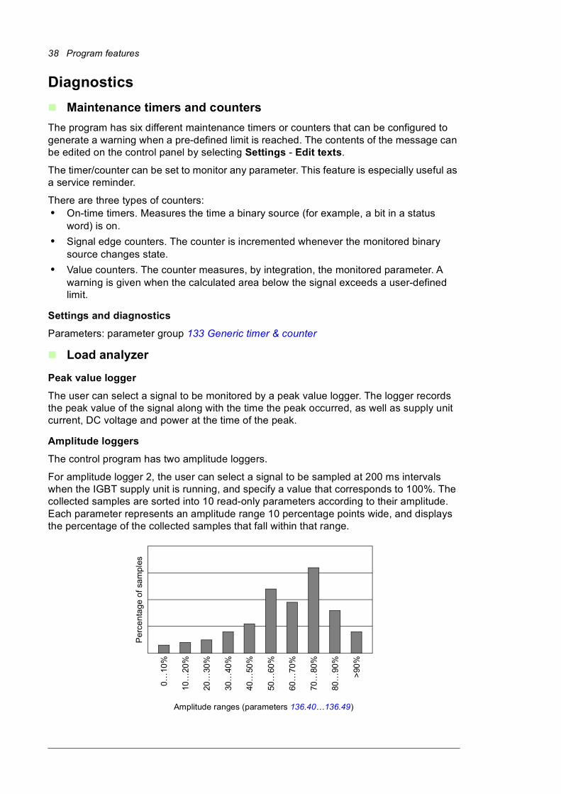
The control program has two amplitude loggers.
For amplitude logger 2, the user can select a signal to be sampled at 200 ms intervals when the IGBT supply unit is running, and specify a value that corresponds to 100%. The collected samples are sorted into 10 read-only parameters according to their amplitude. Each parameter represents an amplitude range 10 percentage points wide, and displays the percentage of the collected samples that fall within that range.
Pe
rce
nta
ge
of
sam
ple
s
0…
10%
10…
20%
20…
30%
30…
40%
40…
50%
50…
60%
60…
70%
70…
80%
80…
90%
>90
%
Amplitude ranges (parameters 136.40…136.49)

Program features 39
Amplitude logger 1 is fixed to monitor the converter current, and cannot be reset. With amplitude logger 1, 100% corresponds to the maximum output current (Imax). The
distribution of samples is shown by parameters 136.20…136.29.
Settings
Parameters: parameter group 136 Load analyzer
User parameter setsThe IGBT supply unit supports four user parameter sets that can be saved to the permanent memory and recalled using parameters. It is also possible to use digital inputs to switch between user parameter sets.
A user parameter set contains all editable values in parameter groups 110…199 except• forced I/O values such as parameters 110.03 DI force selection and 110.04 DI force
data
• I/O extension module settings (groups 114…116)
• fieldbus communication enable parameters (150.01 FBA A enable and 150.31 FBA B enable)
• other fieldbus communication settings (groups 151…156)
• some hardware settings in parameter group 195 HW configuration, and
• user set selection parameters 196.11…196.13.
If no parameter sets have been saved, attempting to load a set will create all sets from the currently active parameter settings.
Switching between user parameter sets is only possible with the supply unit stopped.
Example: Generator power control between two settings: user parameter sets are used, and switching between them is done with DI5.
The parameter settings are:• User set 1: 130.49 is set to -200% (braking power is 100%)
• User set 2: 130.49 is set to 0% (braking power is 0%)
User set 1:• 130.49 is set to -200% (the default value)
• 196.11 is set to Save to set 1
User set 2:• 130.49 is set to 0%
• 196.11 is set to Save to set 2
The final settings are:• 196.11 is set to IO mode
• 196.12 is set to DI5.
Note: Switching between user parameter sets must be done with the supply unit stopped.
Settings
Parameters 196.10…196.13 (page 182).
40 Program features
User lockFor better cybersecurity, it is highly recommended that you set a master pass code to prevent eg. the changing of parameter values and/or the loading of firmware and other files.
WARNING! ABB will not be liable for damages or losses caused by the failure to activate the user lock using a new pass code. See Cybersecurity disclaimer (page 12).
To activate the user lock for the first time, enter the default pass code, 10000000, into 196.02 Pass code. This will make parameters 196.100…196.102 visible. Then enter a new pass code into 196.100 Change user pass code, and confirm the code in 196.101 Confirm user pass code. In 196.102 User lock functionality, define the actions that you want to prevent (we recommend you select all the actions unless otherwise required by the application).
To close the user lock, enter an invalid pass code into 196.02 Pass code, activate 196.08 Control board boot, or cycle the power. With the lock closed, parameters 196.100…196.102 are hidden.
To reopen the lock, enter your pass code into 196.02 Pass code. This will again make parameters 196.100…196.102 visible.
Settings
Parameters 196.02 (page 181) and 196.100…196.102 (page 186).
Data storage parametersTwenty-four (sixteen 32-bit, eight 16-bit) parameters are reserved for data storage. These parameters are unconnected and can be used for linking, testing and commissioning purposes. They can be written to and read from using other parameters’ source or target selections.
Settings and diagnostics
Parameters: parameter group 147 Data storage

Program features 41
ChargingThe charging is always needed to power up the DC link capacitors smoothly. In other words: you may not connect the discharged capacitors to full supply voltage but you must increase the voltage gradually until the capacitors are charged and ready for normal use.
The control program has a function for controlling an additional charging circuit in the IGBT supply unit. The charging function is active as standard, since the cabinet-installed ABB drive which uses IGBT supply unit, needs the additional charging circuit typically.
Note: Some ABB supply and inverter module sizes have internal charging circuit as standard. (Check from the appropriate supply and inverter module hardware manuals.) If all supply and inverter modules connected to the common DC link of the drive have the internal charging circuit, you do not need the common, additional circuit in the supply unit. Then you can also inactivate the charging function of the supply unit (a parameter setting).
When the control program receives the start command (and Run enable and Start enable are on), the control program controls the charging contactor on by a relay output. The contactor connects the input power line to the drive DC link via charging resistors. The DC capacitor charging starts. The DC voltage level in the DC link increases as the charging continues. The charging resistors limit the charging current.
Charging is completed when:• the actual DC voltage exceeds the predefined level (parameter 120.25 MCB closing
level)
• the actual DC voltage change rate is below the predefined level (parameter 120.26 Maximum dU/dt), and
• the pre-defined delay time has passed (parameter 120.27 Start delay).
The control program monitors the charging time. If charging takes more time than defined by a parameter, the supply unit trips to a fault.
If the IGBT supply unit is used in a drive system where the charging must be done by the IGBT supply unit, you must install an additional charging circuit, and activate and tune the charging function in the IGBT supply control program. Consult ABB for more information on tuning the parameters, and the components and wirings needed.
The control program checks that voltage rises after the charging contactor is closed. If the voltage does not rise and the current stays below the level defined with parameter 120.22 Max current for MCB closing, the supply unit trips on fault 3E08 LSU charging (auxiliary code 5). If the current is higher, the supply unit trips on fault 2E09 DC short circuit.
The control program monitors charging attempts to prevent charging circuit overheating. If there are more than two attempts in five minutes to charge the DC link externally, start inhibit is set (106.18 Start inhibit status word, bit 9). After five minutes from the first charging attempt the start inhibit is removed. The supply unit also generates an event selected with parameter 120.50 Charging overload event sel.

42 Program features
Timing diagram
Settings and diagnostics
Signals: 101.01 DC voltage
Parameters: 106.18 Start inhibit status word, 110.24 RO1 source, 120.22 Max current for MCB closing, 120.23 Max DC charging time, 120.25 MCB closing level, 120.26 Maximum dU/dt, 120.27 Start delay, 120.28 MCB relay timing, 120.29 Diode mode, 120.30 External charge enable, 120.50 Charging overload event sel
Warnings: AE85 Charging count
Faults: 2E09 DC short circuit, 3E08 LSU charging, 3E09 Charging count, 5E06 Main contactor Fault
1
3
1 2 3 4
1001h
1h
4
2
107h3h
Udc 100% of nominal
120.25 MCB closing level80% default, range
20…100%
Udc 0% of nominal
DC voltage and current measurements are not active with all power unit types on low DC voltage levels in the beginning of the charging sequence
DC voltage Delay if 120.28 MCB relay timing > 00 s default, range -6…6 s
120.26 Maximum dU/dt50.0 V/s default, range 0.0…200.0 V/s
Charging ready [conditionspassed]
Running on DC voltage control120.22 Max current for
MCB closing5% default, range 0…10%
106.11 Main status wordOnly starting procedure related bits of the 106.11 Main status word are shown in hexadecimal values here. Other values of Main status word are possible depending on control location etc. (eg, bit 9 Remote).
ON command and STARTcommand from active control
location
110.24 RO1 sourceCharging
Charging contactor closing command Delay if 120.28 MCB relay timing < 00 s default, range -6…6 s
110.30 RO3 sourceMCB MCB closing command Delay if 120.28 MCB relay
timing > 00 s default, range -6…6 s
If feedback is missing after supervision delay, fault 5E06 Main contactor Fault is generated.
Start delay for starting of modulation begins after MCB closing feedback (DI3 status is 1)
120.21 Delay for MCB DI3supervision
1 s default, range 0…8 s DI3 status
Running status120.27 Start delay
0.5 s default, range 0…10 s
120.23 Max DC charging time3 s default, range 0…10 s
Charging ready state can not be reached before this time is passed. If charging ready state is not
reached before this time has elapsed, fault 3E08 LSU charging is generated. See auxiliary code in chapter Fault tracing.
Module current
4001h

Program features 43
DDCS communication with inverter unitDDCS communication can be used for transferring data between IGBT supply unit and inverter unit. The DDCS communication and the related transfer media (fiber optic link) are in use in the single drives which consist of one supply unit and one inverter unit. The DDCS link is not in use in multidrives, typically.
You can use the DDCS communication for these purposes:• You can show and adjust the supply unit parameters in the inverter control program
(one interface for the control panel and commissioning engineer).
• You can show supply unit warnings and faults in the inverter control program.
• You can control both the inverter unit and the supply unit through one control interface (for example one fieldbus adapter) in the inverter unit, and transfer the supply unit control commands and references via the link to the supply unit.
For information on using DDCS communication, see section Setting up communication through inverter unit on page 260.
Settings and diagnostics
Parameters: parameter groups 160 DDCS communication, 161 DDCS transmit,162 DDCS receive
Warnings: AE56 INU-LSU comm loss
Faults: 7E0D FA2FA DDCS Com loss

44 Program features
Default I/O connection diagram (BCU)
XD2D Drive-to-drive link1 B
Drive-to-drive link (not in use by default)2 A3 BGND4 ShieldD2D.TERM Drive-to-drive link termination 1)
X485 RS485 connection5 B
Not in use (not in use by default)6 A7 BGND8 ShieldXRO1…XRO3 Relay outputs11 NC XRO1: Charging 2) (Energized = Closes charging contactor.)
250 V AC / 30 V DC / 2 A12 COM13 NO21 NC XRO2: Fault(-1) 3) (Energized = Indicates no fault.)
250 V AC / 30 V DC / 2 A22 COM23 NO31 NC XRO3: MCB ctrl 2) (Energized = Closes main contactor/breaker.)
250 V AC / 30 V DC / 2 A32 COM33 NOXSTO XSTO connector1 OUT XSTO connector. Both circuits (power module, control unit) must be closed for
the supply unit to start. (IN1 and IN2 must be connected to OUT.) 4)2 SGND3 IN14 IN25 IN1
Not in use6 SGND7 IN28 SGNDXDI Digital inputs1 DI1 Temp fault 3) (0 = overtemperature)2 DI2 Run / enable 3) (1 = run / enable)3 DI3 MCB fb 2) (0 = main contactor/breaker open)4 DI4 Not in use by default. Can be used for eg. auxiliary circuit breaker fault5 DI5 Not in use by default. Can be used for eg. earth fault monitoring.6 DI6 Reset 3) (0 -> 1 = fault reset)7 DIIL Not in use by default. Can be used for eg. emergency stop.XDIO Digital input/outputs1 DIO1 Not in use by default2 DIO2 Not in use by default3 DIOGND Digital input/output ground4 DIOGND Digital input/output groundXD24 Auxiliary voltage output5 +24VD +24 V DC 200 mA 5)
6 DICOM Digital input ground7 +24VD +24 V DC 200 mA 5)
8 DIOGND Digital input/output groundDICOM=DIOGND Ground selection switch 6)
XAI Analog inputs, reference voltage output1 +VREF 10 V DC, RL 1…10 kohm2 -VREF -10 V DC, RL 1…10 kohm3 AGND Ground4 AI1+ Not in use by default.
0(2)…10 V, Rin > 200 kohm 7)5 AI1-6 AI2+ Not in use by default.
0(4)…20 mA, Rin = 100 ohm 8)7 AI2-XAO Analog outputs1 AO1
Zero 3) 0…20 mA, RL < 500 ohm2 AGND3 AO2
Zero 3) 0…20 mA, RL < 500 ohm4 AGNDXPOW External power input1 +24VI
24 V DC, 2.05 A2 GND3 +24VI4 GNDX12 Safety functions module connection (not in use in supply units)X13 Control panel connectionX205 Memory unit connection

Program features 45
The table above shows the control connections of the IGBT supply unit, and the default meaning or use of the signals in the control program. Most I/O connections are reserved and wired for the internal use at the factory. Do not change the connections.
Wire sizes and tightening torques: 0.5 … 2.5 mm2 (24…12 AWG) and 0.5 N·m (5 lbf·in) for both stranded and solid wiring.
Notes:1) Switch D2D.TERM. Must be set to ON when the supply unit is the first or last unit on the drive-to-drive (D2D) link. On intermediate supply units, set termination to OFF.
2) Use of the signal in the control program. When parameter 120.30 External charge enable has value Yes (default setting), the control program reserves this I/O terminal for external charging circuit control and monitoring, and parameters 110.24 RO1 source and 110.30 RO3 source are write-protected. If the value is No, you can use the I/O terminal for other purposes.
3) Default use of the signal in the control program. The use can be changed by a parameter. For the delivery-specific use, see the delivery-specific circuit diagrams.
4) The Safe torque off (STO) function is only implemented in the inverter units. When the control board is used in the supply or brake unit, de-energizing IN1 or IN2 of XSTO connector only stops the operation of the supply or brake unit. This stopping is not safety related and can not be used in safety purposes.
5) Total load capacity of these outputs is 4.8 W (200 mA at 24 V) minus the power taken by DIO1 and DIO2.
6) Determines whether DICOM is separated from DIOGND (ie. common reference for digital inputs floats).DICOM=DIOGND ON: DICOM connected to DIOGND. OFF: DICOM and DIOGND separate.7) Current [0(4)…20 mA, Rin = 100 ohm] or voltage [0(2)…10 V, Rin > 200 kohm] input selected by switch AI1.
Change of setting requires reboot of control unit.
8) Current [0(4)…20 mA, Rin = 100 ohm] or voltage [0(2)…10 V, Rin > 200 kohm] input selected by switch AI2.
Change of setting requires reboot of control unit.
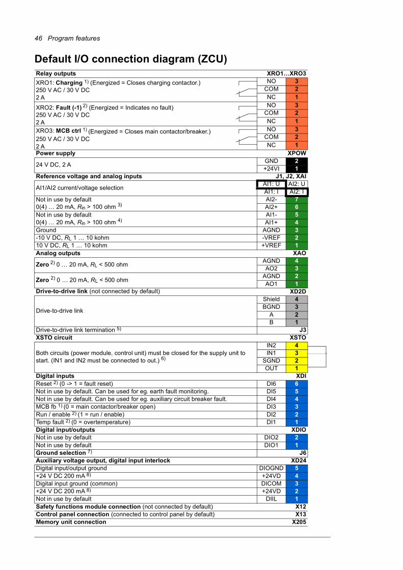
46 Program features
Default I/O connection diagram (ZCU)Relay outputs XRO1…XRO3
XRO1: Charging 1) (Energized = Closes charging contactor.) 250 V AC / 30 V DC2 A
NO 3COM 2NC 1
XRO2: Fault (-1) 2) (Energized = Indicates no fault)250 V AC / 30 V DC2 A
NO 3COM 2NC 1
XRO3: MCB ctrl 1) (Energized = Closes main contactor/breaker.)250 V AC / 30 V DC2 A
NO 3COM 2NC 1
Power supply XPOW
24 V DC, 2 AGND 2+24VI 1
Reference voltage and analog inputs J1, J2, XAI
AI1/AI2 current/voltage selectionAI1: U AI2: UAI1: I AI2: I
Not in use by default0(4) … 20 mA, Rin > 100 ohm 3)
AI2- 7AI2+ 6
Not in use by default0(4) … 20 mA, Rin > 100 ohm 4)
AI1- 5AI1+ 4
Ground AGND 3-10 V DC, RL 1 … 10 kohm -VREF 210 V DC, RL 1 … 10 kohm +VREF 1Analog outputs XAO
Zero 2) 0 … 20 mA, RL < 500 ohmAGND 4AO2 3
Zero 2) 0 … 20 mA, RL < 500 ohmAGND 2AO1 1
Drive-to-drive link (not connected by default) XD2D
Drive-to-drive link
Shield 4BGND 3
A 2B 1
Drive-to-drive link termination 5) J3XSTO circuit XSTO
Both circuits (power module, control unit) must be closed for the supply unit to start. (IN1 and IN2 must be connected to out.) 6)
IN2 4IN1 3
SGND 2OUT 1
Digital inputs XDIReset 2) (0 -> 1 = fault reset) DI6 6Not in use by default. Can be used for eg. earth fault monitoring. DI5 5Not in use by default. Can be used for eg. auxiliary circuit breaker fault. DI4 4MCB fb 1) (0 = main contactor/breaker open) DI3 3Run / enable 2) (1 = run / enable) DI2 2Temp fault 2) (0 = overtemperature) DI1 1Digital input/outputs XDIONot in use by default DIO2 2Not in use by default DIO1 1Ground selection 7) J6Auxiliary voltage output, digital input interlock XD24Digital input/output ground DIOGND 5+24 V DC 200 mA 8) +24VD 4Digital input ground (common) DICOM 3+24 V DC 200 mA 8) +24VD 2Not in use by default DIIL 1Safety functions module connection (not connected by default) X12Control panel connection (connected to control panel by default) X13Memory unit connection X205
Program features 47
The table above shows the control connections of the IGBT supply unit, and the default meaning or use of the signals in the control program. Most I/O connections are reserved and wired for the internal use at the factory. Do not change the connections.
Wire sizes and tightening torques: 0.5 … 2.5 mm2 (24…12 AWG) and 0.5 N·m (5 lbf·in) for both stranded and solid wiring.
Notes:1) Use of the signal in the control program. When parameter 120.30 External charge enable has value Yes (default setting), the control program reserves this I/O terminal for external charging circuit control and monitoring, and parameters 110.24 RO1 source and 110.30 RO3 source are write-protected. If the value is No, you can use the I/O terminal for other purposes
2) Default use of the signal in the control program. The use can be changed by a parameter. For the delivery-specific use, see the delivery-specific circuit diagrams.
3) Current [0(4)…20 mA, Rin > 100 ohm] or voltage [0(2)…10 V, Rin > 200 kohm] input selected by jumper J2.
Change of setting requires reboot of control unit.
4) Current [0(4)…20 mA, Rin > 100 ohm] or voltage [0(2)…10 V, Rin > 200 kohm] input selected by jumper J1.
Change of setting requires reboot of control unit.
5) Jumper/switch J3. Enable bus termination on the supply units at the ends of the drive-to-drive (D2D) link. On intermediate supply units, disable bus termination.ZCU-14: Termination disabled. Termination enabled.
6) The Safe torque off (STO) function is only implemented in the inverter units. When the control board is used in the supply or brake unit, de-energizing IN1 or IN2 of XSTO connector only stops the operation of the supply or brake unit. This stopping is not safety related and can not be used in safety purposes.
7) Jumper/switch J6. Determines whether DICOM is separated from DIOGND (ie. common reference for digital inputs floats).ZCU-14: DICOM connected to DIOGND. DICOM and DIOGND separate.
8) Total load capacity of these outputs is 4.8 W (200 mA at 24 V) minus the power taken by DIO1 and DIO2.
Parameters that define the use of relay outputs
The table below shows the relay outputs and the parameters and that define their use by default.
Parameters that define the use of digital inputs
The table below shows the default use of digital inputs by parameters.
Output Parameter Default value
RO1 110.24 RO1 source Charging
RO2 110.27 RO2 source Fault (-1)
RO3 110.30 RO3 source MCB
Input Parameter Additional information
DI1 131.33 Cabinet temperature fault source 0 = overtemperature
Typically this is used for monitoring the status of cabinet temperature fault.
DI2 120.12 Run enable 1 source
120.03 Ext1 in1 source
1 = run enable
1 = on
DI6 131.11 Fault reset selection 0 -> 1 = fault reset
48 Program features
The table below shows the common use of the remaining digital inputs in the cabinet installed drives by ABB. Note that these are no default parameters settings in the control program.
For the rest of the parameters that can use digital inputs as signal source, see chapter Parameters.
Input Parameter Additional information
DI4 131.32 Aux circuit breaker fault source 0 = auxiliary circuit breaker or switch open
Typically this is used for monitoring the status of auxiliary circuit breaker.
DI5 131.28 Ext earth leakage signal source 0 = earth leakage current monitoring tripped
DIIL 121.05 Emergency stop source 0 = emergency stop active

Program features 49
Power share with droop controlIf two supply units that are fed from separate transformers are connected to the same DC link, you must make sure that the power share is controlled and the system remains stable. Always use the same DC voltage reference for all units. Use also the droop function in all units.
The droop function stabilizes the load sharing between the units. It automatically tunes the external DC voltage reference slightly as the actual load of the unit varies: it changes the reference in the generating mode and in the motoring mode. See the diagram below. When the droop is active in all units, their reference corrections help in finding the right load balance and remain it automatically.
With the droop control enabled, two supply units can control the same DC link voltage. DC voltage reference droop is implemented by modifying the DC link voltage reference depending on actual power with droop rate. The droop increases the DC link voltage in generator-side and decreases it in motoring side. Droop control is defined by parameters 123.30 Udc-ctrl droop and 123.31 Udc-ctrl drooping rate. The default drooping rate is 5% of nominal phase peak voltage. With nominal motor-side power the DC link reference is decreased:
Some examples of needed marginal for DC reference with 5% drooping rate are given in the table below. See also the diagram below.
If the AC grid voltage is higher, more marginal is needed since phase-to-phase peak grid voltage is the lowest DC voltage that the supply unit can produce. Producing capacitive reactive power requires DC voltage and DC voltage marginal that are higher than usual default values. See also section Reactive power control on page 30.
AC line voltage DC voltage Minimum DC voltage
Droop marginal DC reference (see parameter 123.01)
415 V 616 V · 415 · 1.05 17 V 616 V +17 V = 633 V
500 V 742 V · 500 · 1.05 20 V 742 V + 20 V = 762 V
690 V 1025 V · 690 · 1.05 28 V 1025 V + 28 V = 1053 V
0.05 · 2/3 · 500 V 20 V ����
2
2
2
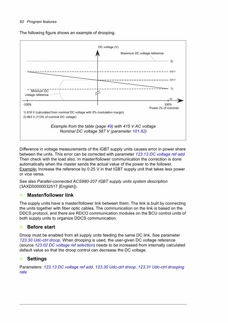
50 Program features
The following figure shows an example of drooping.
Difference in voltage measurements of the IGBT supply units causes error in power share between the units. This error can be corrected with parameter 123.13 DC voltage ref add. Then check with the load also. In master/follower communication the correction is done automatically when the master sends the actual value of the power to the follower. Example: Increase the reference by 0.25 V in that IGBT supply unit that takes less power or vice versa.
See also Parallel-connected ACS880-207 IGBT supply units system description (3AXD50000032517 [English]).
Master/follower link
The supply units have a master/follower link between them. The link is built by connecting the units together with fiber optic cables. The communication on the link is based on the DDCS protocol, and there are RDCO communication modules on the BCU control units of both supply units to organize DDCS communication.
Before start
Droop must be enabled from all supply units feeding the same DC link. See parameter 123.30 Udc-ctrl droop. When drooping is used, the user-given DC voltage reference (source 123.02 DC voltage ref selection) needs to be increased from internally calculated default value so that the droop control can decrease the DC voltage.
Settings
Parameters: 123.13 DC voltage ref add, 123.30 Udc-ctrl droop, 123.31 Udc-ctrl drooping rate
650 V
-100% 100%
633 V
0V
DC voltage (V)
Maximum DC voltage reference
Power (% of nominal)
Minimum DCvoltage reference
2)
1)
1) 616 V (calculated from nominal DC voltage with 5% modulation margin)
2) 663 V (113% of nominal DC voltage)
Example from the table (page 49) with 415 V AC voltageNominal DC voltage 587 V (parameter 101.62)
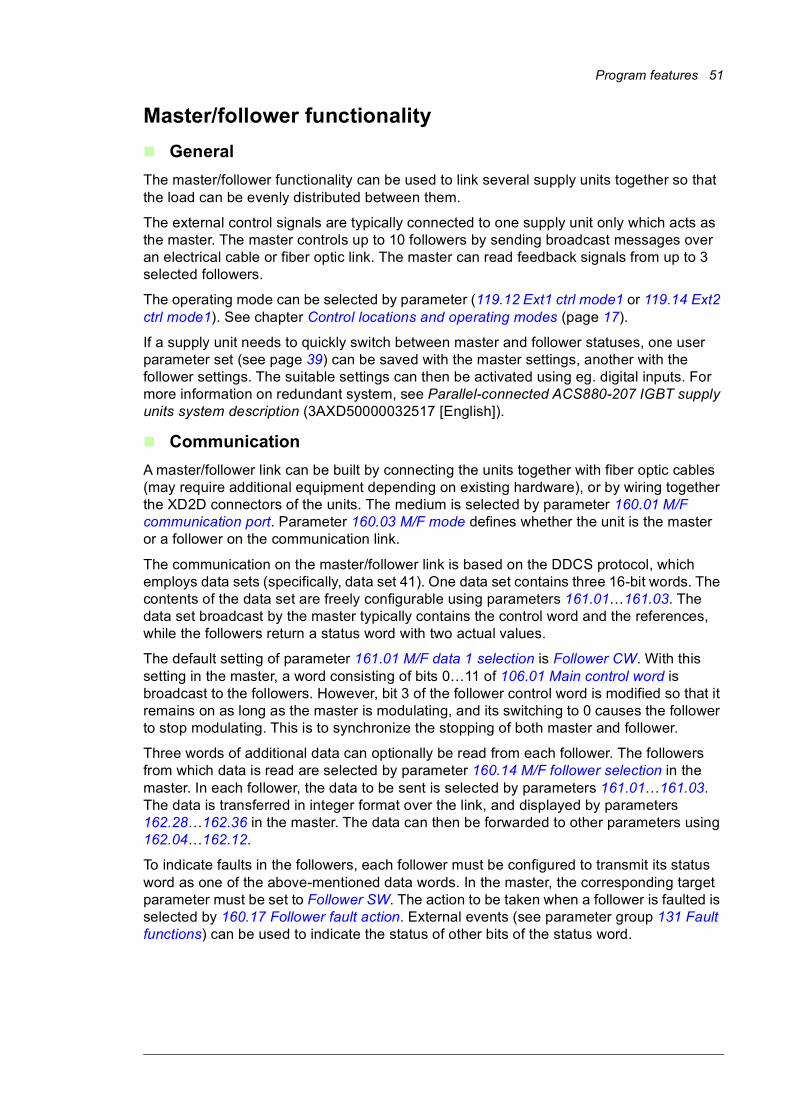
Program features 51
Master/follower functionality
General
The master/follower functionality can be used to link several supply units together so that the load can be evenly distributed between them.
The external control signals are typically connected to one supply unit only which acts as the master. The master controls up to 10 followers by sending broadcast messages over an electrical cable or fiber optic link. The master can read feedback signals from up to 3 selected followers.
The operating mode can be selected by parameter (119.12 Ext1 ctrl mode1 or 119.14 Ext2 ctrl mode1). See chapter Control locations and operating modes (page 17).
If a supply unit needs to quickly switch between master and follower statuses, one user parameter set (see page 39) can be saved with the master settings, another with the follower settings. The suitable settings can then be activated using eg. digital inputs. For more information on redundant system, see Parallel-connected ACS880-207 IGBT supply units system description (3AXD50000032517 [English]).
Communication
A master/follower link can be built by connecting the units together with fiber optic cables (may require additional equipment depending on existing hardware), or by wiring together the XD2D connectors of the units. The medium is selected by parameter 160.01 M/F communication port. Parameter 160.03 M/F mode defines whether the unit is the master or a follower on the communication link.
The communication on the master/follower link is based on the DDCS protocol, which employs data sets (specifically, data set 41). One data set contains three 16-bit words. The contents of the data set are freely configurable using parameters 161.01…161.03. The data set broadcast by the master typically contains the control word and the references, while the followers return a status word with two actual values.
The default setting of parameter 161.01 M/F data 1 selection is Follower CW. With this setting in the master, a word consisting of bits 0…11 of 106.01 Main control word is broadcast to the followers. However, bit 3 of the follower control word is modified so that it remains on as long as the master is modulating, and its switching to 0 causes the follower to stop modulating. This is to synchronize the stopping of both master and follower.
Three words of additional data can optionally be read from each follower. The followers from which data is read are selected by parameter 160.14 M/F follower selection in the master. In each follower, the data to be sent is selected by parameters 161.01…161.03. The data is transferred in integer format over the link, and displayed by parameters 162.28…162.36 in the master. The data can then be forwarded to other parameters using 162.04…162.12.
To indicate faults in the followers, each follower must be configured to transmit its status word as one of the above-mentioned data words. In the master, the corresponding target parameter must be set to Follower SW. The action to be taken when a follower is faulted is selected by 160.17 Follower fault action. External events (see parameter group 131 Fault functions) can be used to indicate the status of other bits of the status word.

52 Program features
Construction of the master/follower link
The master/follower link is formed by connecting the units together using either• shielded twisted-pair cable between the XD2D terminals*, or
• fiber optic cables. Supply units with a ZCU control unit require an additional FDCO DDCS communication module; supply units with a BCU control unit require an RDCO module.
*This connection cannot co-exist, and is not to be confused with, drive-to-drive (D2D) communication implemented by application programming (detailed in Drive application programming manual (IEC 61131-3), 3AUA0000127808 [English]).
Connection examples are shown below. Note that a star configuration using fiber optic cables requires an NDBU-95C DDCS branching unit.
Master/follower wiring with electrical cable
Master
Termination ON
1 2 3 41 2 3 4 1 2 3 4
XD
2D
B XD
2D
XD
2D
A
BG
ND
Shi
eld B A
BG
ND
Shi
eld B A
BG
ND
Shi
eld
Follower 1
Termination OFF
Follower n
Termination ON
See the hardware manual for wiring and termination details.
Ring configuration with fiber optic cables
T = Transmitter; R = Receiver
Follower 2
(ZCU) Control unit
FDCO
RT
Follower 1
(BCU) Control unit
RDCO
RTCH2
Master
(ZCU) Control unit
FDCO
RT
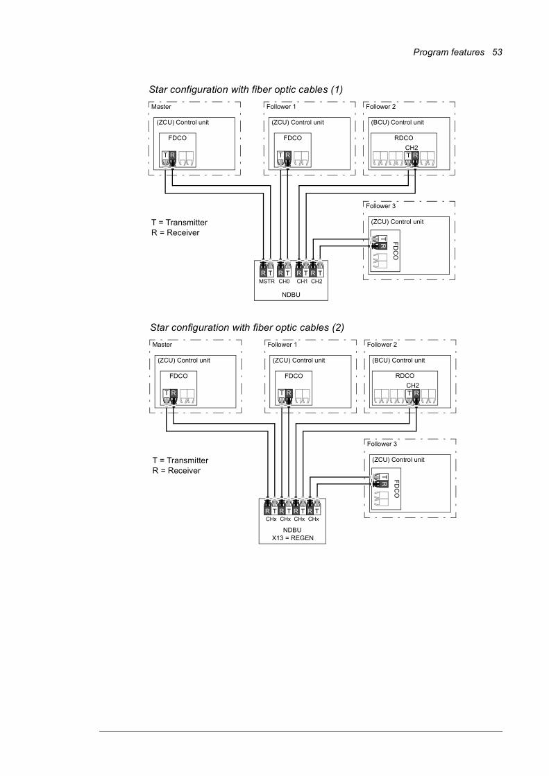
Program features 53
Follower 3
(ZCU) Control unit
FD
CO
Follower 1
Star configuration with fiber optic cables (1)
T = TransmitterR = Receiver
NDBU
MSTR CH0 CH1 CH2
R T R T R T R T
RT
(ZCU) Control unit
Follower 2
(BCU) Control unit
RDCO
RTCH2
FDCO
RT
Master
(ZCU) Control unit
FDCO
RT
Follower 3
(ZCU) Control unit
FD
CO
Follower 1
Star configuration with fiber optic cables (2)
T = TransmitterR = Receiver
NDBU
CHx CHxR T R T
RT
(ZCU) Control unit
Follower 2
(BCU) Control unit
RDCO
RTCH2
FDCO
RT
Master
(ZCU) Control unit
FDCO
RT
CHx CHxR T R T
X13 = REGEN

54 Program features
Example parameter settings
The following is a checklist of parameters that need to be set when configuring the master/follower link. In this example, the master broadcasts the Follower control word and the references. The follower returns a status word and two actual values (this is not compulsory but is shown for clarity).
Master settings:• Master/follower link activation
• 160.01 M/F communication port (fiber optic channel or XD2D selection)
• (160.02 M/F node address = 1)
• 160.03 M/F mode = DDCS master (for both fiber optic and wire connection)
• 160.05 M/F HW connection (Ring or Star for fiber optic, Star for wire)
• Data to be broadcast to the followers
• 161.01 M/F data 1 selection = Follower CW (Follower control word)
• 161.02 M/F data 2 selection = Master power
• Data to be read from the followers (optional)
• 160.14 M/F follower selection (selection of followers that data is read from)
• 162.04 Follower node 2 data 1 sel … 162.12 Follower node 4 data 3 sel (mapping of data received from followers)
Follower settings:• Master/follower link activation
• 160.01 M/F communication port (fiber optic channel or XD2D selection)
• 160.02 M/F node address = 2…60
• 160.03 M/F mode = DDCS follower (for both fiber optic and wire connection)
• 160.05 M/F HW connection (Ring or Star for fiber optic, Star for wire)
• Mapping of data received from master
• 162.01 M/F data 1 selection = CW 16bit
• 162.02 M/F data 2 selection = Ref1 16bit
• 162.03 M/F data 3 selection = Ref2 16bit
• Selection of operating mode
• 119.12 Ext1 ctrl mode1 = DC control or Power control
• Selection of data to be sent to master (optional)
• 161.01 M/F data 1 selection = SW 16bit
• 161.02 M/F data 2 selection = Act1 16bit
• 161.03 M/F data 3 selection = Act2 16bit

Program features 55
Specifications of the fiber optic master/follower link
• Maximum fiber optic cable length:
• FDCO-01/02 or RDCO-04 with POF (Plastic Optic Fiber): 30 m
• FDCO-01/02 or RDCO-04 with HCS (Hard-clad Silica Fiber): 200 m
• For distances up to 1000 m, use two NOCR-01 optical converter/repeaters with glass optic cable (GOF, 62.5 micrometers, Multi-Mode)
• Maximum shielded twisted-pair cable length: 50 m
• Transmission rate: 4 Mbit/s
• Total performance of the link: < 5 ms to transfer references between the master and followers.
• Protocol: DDCS (Distributed Drives Communication System)
Settings and diagnostics
Parameter groups 160 DDCS communication (page 158), 161 DDCS transmit (page 164) and 162 DDCS receive (page 168)
Warnings: AE81 MF comm loss, AE82 Follower
Faults: FE06 MF communication loss, FE07 Follower drive failure
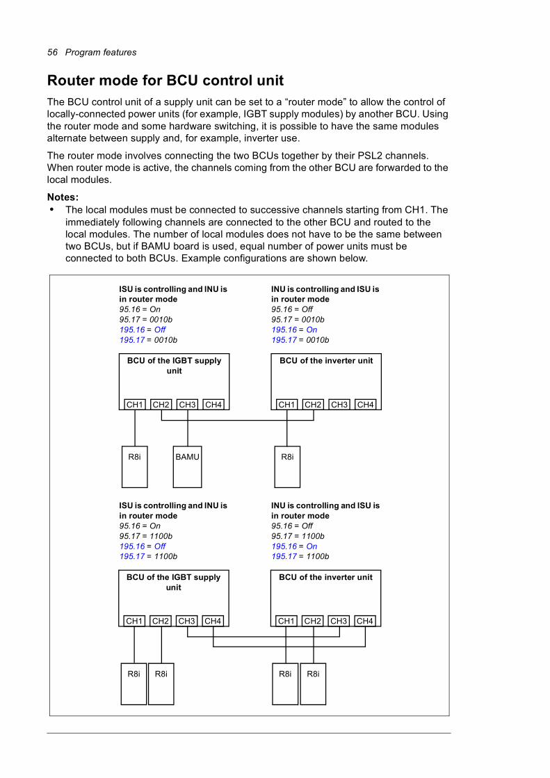
56 Program features
Router mode for BCU control unitThe BCU control unit of a supply unit can be set to a “router mode” to allow the control of locally-connected power units (for example, IGBT supply modules) by another BCU. Using the router mode and some hardware switching, it is possible to have the same modules alternate between supply and, for example, inverter use.
The router mode involves connecting the two BCUs together by their PSL2 channels. When router mode is active, the channels coming from the other BCU are forwarded to the local modules.
Notes:• The local modules must be connected to successive channels starting from CH1. The
immediately following channels are connected to the other BCU and routed to the local modules. The number of local modules does not have to be the same between two BCUs, but if BAMU board is used, equal number of power units must be connected to both BCUs. Example configurations are shown below.
ISU is controlling and INU is in router mode95.16 = On95.17 = 0010b195.16 = Off195.17 = 0010b
CH1 CH2 CH3 CH4 CH1 CH2 CH3 CH4
INU is controlling and ISU is in router mode95.16 = Off95.17 = 0010b195.16 = On195.17 = 0010b
BCU of the IGBT supply unit
BCU of the inverter unit
BAMU
ISU is controlling and INU is in router mode95.16 = On95.17 = 1100b195.16 = Off195.17 = 1100b
CH1 CH2 CH3 CH4 CH1 CH2 CH3 CH4
R8i
INU is controlling and ISU is in router mode95.16 = Off95.17 = 1100b195.16 = On195.17 = 1100b
BCU of the IGBT supply unit
BCU of the inverter unit
R8i R8i R8i
R8i R8i

Program features 57
• When BAMU board is used, it must be connected to the last channel of the BCU of the IGBT supply unit.
• The maximum number of channels is 10, and it does not increase when router mode is used.
• In PLC control, any switchovers must be done in stopped state, and so that at least one BCU is in router mode at any given time.
Settings
Parameters 195.16 Router mode and 195.17 Router channel config (page 178).
Distributed I/O busDistributed I/O bus controls and supervises each cabinet fan separately. It detects malfunctioning fans and indicates them with warning or fault messages. The distributed I/O bus is controlled by CIO-01 I/O module. For more information, see CIO-01 I/O module for distributed I/O bus control user’s manual (3AXD50000126880 [English]).
Settings
Parameter groups 206 I/O bus configuration, 207 I/O bus service, 208 I/O bus diagnostics and 209 I/O bus fan identification (page 187).
Similar supervisions to the ones activated from parameters 131.38 Fuse trip fault source and 131.39 Brake chopper fault source (page 135) via standard I/O can be activated also via distributed I/O.
Distributed I/O is available for liquid-cooled units only.

58 Program features

Parameters 59
6
Parameters
What this chapter containsThe chapter describes the parameters, including actual signals, of the control program.
Terms and abbreviationsTerm Definition
Actual signal Type of parameter that is the result of a measurement or calculation by the IGBT supply unit, or contains status information. Most actual signals are read-only, but some (especially counter-type actual signals) can be reset.
Def (In the following table, shown on the same row as the parameter name)
The default value of a parameter.
FbEq16 (In the following table, shown on the same row as the parameter range, or for each selection)
16-bit fieldbus equivalent: The scaling between the integer used in communication and the value shown on the panel when a 16-bit value is selected for transmission to an external system.
A dash (-) indicates that the parameter is not accessible in 16-bit format.
The corresponding 32-bit scalings are listed in chapter Additional parameter data (page 189).
Other The value is taken from another source.
Parameter Either an user-adjustable operating instruction for the IGBT supply unit, or an actual signal.
p.u. Per unit

60 Parameters
Reserved digital inputs and relay outputs For the cabinet-installed unit, digital inputs and relay outputs are typically defined in use and connected to the appropriate control circuits already at the factory. Do not change the settings of the reserved digital inputs or relay outputs. See the delivery-specific circuit diagrams and subsections Default I/O connection diagram (BCU) on page 44, and Default I/O connection diagram (ZCU) on page 46.

Parameters 61
Summary of parameter groupsGroup Contents Page
101 Actual values Basic signals for monitoring of the IGBT supply unit. 63
103 Input references Values of references received from various sources. 65
104 Warnings and faults Information on warnings and faults that occurred last. 66
105 Diagnostics Various run-time-type counters and measurements related to IGBT supply unit maintenance.
71
106 Control and status words Control and status words. 72
107 System info Hardware and firmware information. 78
110 Standard DI, RO Configuration of digital inputs and relay outputs. 79
111 Standard DIO, FI, FO Configuration of digital input/outputs and frequency inputs/outputs. 83
112 Standard AI Configuration of standard analog inputs. 86
113 Standard AO Configuration of analog outputs. 89
114 Extension I/O module 1 Configuration of I/O extension module 1. 92
115 Extension I/O module 2 Configuration of I/O extension module 2. 107
116 Extension I/O module 3 Configuration of I/O extension module 3. 111
119 Operation mode Selection of external control location sources and operating modes.
114
120 Start/stop Start/stop and run/start enable signal source selection; charging settings.
115
121 Start/stop mode Emergency stop settings. 120
122 Power reference Settings of the active power reference chain. 120
123 DC voltage reference Settings of the DC voltage reference chain. 122
124 Reactive power reference Settings of the reactive power reference chain. 123
130 Limits Operation limits of the IGBT supply unit. 127
131 Fault functions Settings that define the behavior of the IGBT supply unit upon fault situations.
131
133 Generic timer & counter Configuration of maintenance timers/counters. 137
136 Load analyzer Peak value and amplitude logger settings. 142
146 Monitoring settings Scaling settings. 145
147 Data storage Parameters that can be written to and read from by using source and target settings of other parameters.
146
149 Panel port communication Communication settings for the control panel port. 148
150 FBA General settings for fieldbus communication configuration. 148
151 FBA A settings Fieldbus adapter A configuration. 153
152 FBA A data in Selection of data to be transferred from IGBT supply unit to fieldbus controller through fieldbus adapter A.
154
153 FBA A data out Selection of data to be transferred from fieldbus controller to IGBT supply unit through fieldbus adapter A.
155
154 FBA B settings Fieldbus adapter B configuration. 155
155 FBA B data in Selection of data to be transferred from IGBT supply unit to fieldbus controller through fieldbus adapter B.
157
156 FBA B data out Selection of data to be transferred from fieldbus controller to IGBT supply unit through fieldbus adapter B.
157
160 DDCS communication DDCS communication configuration. 158
161 DDCS transmit Defines the data sent to the DDCS link. 164
162 DDCS receive Mapping of data received through the DDCS link. 168
190 BAMU measurements Grid measurement signals from BAMU measurement unit. 175
191 BAMU configuration Settings for BAMU measurement unit. 176
195 HW configuration Various hardware-related settings. 177

62 Parameters
196 System Language selection; parameter save and restore; control unit reboot; user lock.
181
199 Off grid configuration Configuration of the optimal grid control functionality. 187
206 I/O bus configuration
207 I/O bus service
208 I/O bus diagnostics
209 I/O bus fan identification
Distributed I/O bus settings. 187
Group Contents Page

Parameters 63
Parameter listingNo. Name/Value Description Def/FbEq16
101101 Actual values Basic signals for monitoring of the IGBT supply unit.
All parameters in this group are read-only unless otherwise noted.
101.01 DC voltage Measured intermediate circuit voltage in Volts. -
0.00 … 2000.00 V Measured intermediate circuit voltage. See par. 146.04
101.02 Line current Estimated line current in Amperes. -
- Estimated line current. 1 = 1 A
101.03 Line current % Estimated line current in percent of the nominal value.
0.0 … 1000.0% Estimated line current in percent of the nominal value. 1 = 1%
101.04 Active current Estimated fundamental frequency active current in Amperes. -
- Estimated fundamental frequency active current. See par. 146.01
101.05 Active current % Estimated active current in percent of the nominal value. -
-1000.0 … 1000.0% Estimated active current in percent of the nominal value. 1 = 1%
101.06 Reactive current Estimated reactive current in Amperes. -
- Estimated reactive current. See par. 146.02
101.07 Reactive current % Estimated reactive current in percent of the nominal value. -
-1000.0 … 1000.0% Estimated reactive current in percent of the nominal value. 1 = 1%
101.08 Frequency Estimated frequency of power supply network. -
0.00…100.00 Hz Estimated frequency of power supply network. 100 = 1 Hz
101.09 Grid voltage Estimated voltage of power supply network in Volts. -
0.00…1000.00 V Estimated voltage of power supply network. 1 = 1 V
101.10 Apparent power Estimated apparent power in kVA. -
- Estimated apparent power. 1 = 1 kVA
101.11 Apparent power % Estimated apparent power in percent of the nominal value. -
-1000.0 … 1000.0% Estimated apparent power in percent of the nominal value. 1 = 1%
101.12 Power Estimated IGBT supply unit fundamental frequency power in kW. Sign can be changed with parameter 130.47 Power sign change.(positive = power flow from power supply network to intermediate circuit,negative = power flow from intermediate circuit to power supply network)
-
- Estimated IGBT supply unit fundamental frequency power. See par. 146.01
101.13 Power % Estimated fundamental frequency input power in percent of the nominal value.
-
-1000.0 … 1000.0% Estimated fundamental frequency input power in percent of the nominal value.
1 = 1%
101.14 Reactive power Estimated reactive power in kVAr.(positive = capacitive, negative = inductive)
-
- Estimated reactive power. See par. 146.02
101.15 Reactive power % Estimated reactive power in percent. -
-1000.0 … 1000.0% Estimated reactive power in percent. 1 = 1%
101.16 CosPhi Cos phi. -
-1.00 … 1.00 Cos phi. 100 = 1
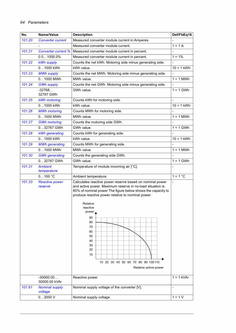
64 Parameters
101.20 Converter current Measured converter module current in Amperes. -
- Measured converter module current. 1 = 1 A
101.21 Converter current % Measured converter module current in percent. -
0.0…1000.0% Measured converter module current in percent. 1 = 1%
101.22 kWh supply Counts the net kWh. Motoring side minus generating side. -
0…1000 kWh kWh value. 10 = 1 kWh
101.23 MWh supply Counts the net MWh. Motoring side minus generating side. -
0…1000 MWh MWh value. 1 = 1 MWh
101.24 GWh supply Counts the net GWh. Motoring side minus generating side. -
-32768… 32767 GWh
GWh value. 1 = 1 GWh
101.25 kWh motoring Counts kWh for motoring side. -
0…1000 kWh kWh value. 10 = 1 kWh
101.26 MWh motoring Counts MWh for motoring side. -
0…1000 MWh MWh value. 1 = 1 MWh
101.27 GWh motoring Counts the motoring side GWh. -
0…32767 GWh GWh value. 1 = 1 GWh
101.28 kWh generating Counts kWh for generating side. -
0…1000 kWh kWh value. 10 = 1 kWh
101.29 MWh generating Counts MWh for generating side. -
0…1000 MWh MWh value. 1 = 1 MWh
101.30 GWh generating Counts the generating side GWh. -
0…32767 GWh GWh value. 1 = 1 GWh
101.31 Ambient temperature
Temperature of module incoming air [°C]. -
0…100 °C Ambient temperature. 1 = 1 °C
101.33 Reactive power reserve
Calculates reactive power reserve based on nominal power and active power. Maximum reserve in no-load situation is 80% of nominal power The figure below shows the capacity to produce reactive power relative to nominal power.
-
-30000.00… 30000.00 kVAr
Reactive power. 1 = 1 kVAr
101.61 Nominal supply voltage
Nominal supply voltage of the converter [V]. -
0…2000 V Nominal supply voltage. 1 = 1 V
No. Name/Value Description Def/FbEq16
Relativereactive
power
Relative active power
10
2030
40
50
60
70
80
90
10 20 30 40 50 60 70 80 90 100110

Parameters 65
101.62 Nominal DC voltage Nominal DC voltage of the converter [V]. -
0…2000 V Nominal DC voltage. 1 = 1 V
101.63 Nominal current Nominal current from the supply modules before LCL filter [A]. -
0…30000 A Nominal current. 1 = 1 A
101.64 Nominal power Nominal power of the converter [V]. -
0…30000 kW Nominal power. 1 = 1 kW
101.70 Ambient temperature %
Ambient temperature of supply unit in percent. 0…100% corresponds to 0…60 °C or 32…140 °F.
See also 101.31 Ambient temperature.
-
-200.00…200.00% Ambient temperature in percent. 100 = 1%
103103 Input references Values of references received from various sources.
All parameters in this group are read-only unless otherwise noted.
103.01 Panel reference Reference 1 given from the control panel. -
-100000.00 … 100000.00
Control panel reference. 1 = 10
103.05 FB A reference 1 Scaled fieldbus A reference 1. -
-100000.00 … 100000.00
Fieldbus A reference 1. 1 = 10
103.06 FB A reference 2 Scaled fieldbus A reference 2. -
-100000.00 … 100000.00
Fieldbus A reference 2. 1 = 10
103.07 FB B reference 1 Scaled fieldbus B reference 1. -
-100000.00 … 100000.00
Fieldbus B reference 1. 1 = 10
103.08 FB B reference 2 Scaled fieldbus B reference 2. -
-100000.00 … 100000.00
Fieldbus B reference 2. 1 = 10
103.11 DDCS controller ref 1
Reference 1 received from the external (DDCS) controller. The value has been scaled according to parameter 160.60 DDCS controller ref1 type.
See also section Setting up communication through inverter unit on page 260.
-
-30000.00 … 30000.00
Scaled reference 1 received from external controller. 1 = 10
103.12 DDCS controller ref 2
Reference 2 received from the external (DDCS) controller. The value has been scaled according to parameter 160.61 DDCS controller ref2 type.
See also section Setting up communication through inverter unit on page 260.
-
-30000.00 … 30000.00
Scaled reference 2 received from external controller. 1 = 10
103.13 M/F or D2D ref1 Master/follower reference 1 received from the master. The value has been scaled according to parameter 160.10 M/F ref1 type.See also section Master/follower functionality (page 51).
1 = 10
-30000.00 … 30000.00
Scaled reference 1 received from master. 1 = 10
103.14 M/F or D2D ref2 Master/follower reference 2 received from the master. The value has been scaled according to parameter 160.11 M/F ref2 type.
1 = 10
-30000.00 … 30000.00
Scaled reference 2 received from master. 1 = 10
No. Name/Value Description Def/FbEq16

66 Parameters
104104 Warnings and faults Information on warnings and faults that occurred last.
For explanations of individual warning and fault codes, see chapter Fault tracing.
All parameters in this group are read-only unless otherwise noted.
104.01 Tripping fault Code of the 1st active fault (the fault that caused the current trip).
-
0000h…FFFFh 1st active fault. 1 = 1
104.02 Active fault 2 Code of the 2nd active fault. -
0000h…FFFFh 2nd active fault. 1 = 1
104.03 Active fault 3 Code of the 3rd active fault. -
0000h…FFFFh 3rd active fault. 1 = 1
104.04 Active fault 4 Code of the 4th active fault. -
0000h…FFFFh 4th active fault. 1 = 1
104.05 Active fault 5 Code of the 5th active fault. -
0000h…FFFFh 5th active fault. 1 = 1
104.06 Active warning 1 Code of the 1st active warning. -
0000h…FFFFh 1st active warning. 1 = 1
104.07 Active warning 2 Code of the 2nd active warning. -
0000h…FFFFh 2nd active warning. 1 = 1
104.08 Active warning 3 Code of the 3rd active warning. -
0000h…FFFFh 3rd active warning. 1 = 1
104.09 Active warning 4 Code of the 4th active warning. -
0000h…FFFFh 4th active warning. 1 = 1
104.10 Active warning 5 Code of the 5th active warning. -
0000h…FFFFh 5th active warning. 1 = 1
104.11 Latest fault Code of the 1st stored (non-active) fault. -
0000h…FFFFh 1st stored fault. 1 = 1
104.12 2nd latest fault Code of the 2nd stored (non-active) fault. -
0000h…FFFFh 2nd stored fault. 1 = 1
104.13 3rd latest fault Code of the 3rd stored (non-active) fault. -
0000h…FFFFh 3rd stored fault. 1 = 1
104.14 4th latest fault Code of the 4th stored (non-active) fault. -
0000h…FFFFh 4th stored fault. 1 = 1
104.15 5th latest fault Code of the 5th stored (non-active) fault. -
0000h…FFFFh 5th stored fault. 1 = 1
104.16 Latest warning Code of the 1st stored (non-active) warning. -
0000h…FFFFh 1st stored warning. 1 = 1
104.17 2nd latest warning Code of the 2nd stored (non-active) warning. -
0000h…FFFFh 2nd stored warning. 1 = 1
104.18 3rd latest warning Code of the 3rd stored (non-active) warning. -
0000h…FFFFh 3rd stored warning. 1 = 1
104.19 4th latest warning Code of the 4th stored (non-active) warning. -
0000h…FFFFh 4th stored warning. 1 = 1
104.20 5th latest warning Code of the 5th stored (non-active) warning. -
0000h…FFFFh 5th stored warning. 1 = 1
No. Name/Value Description Def/FbEq16
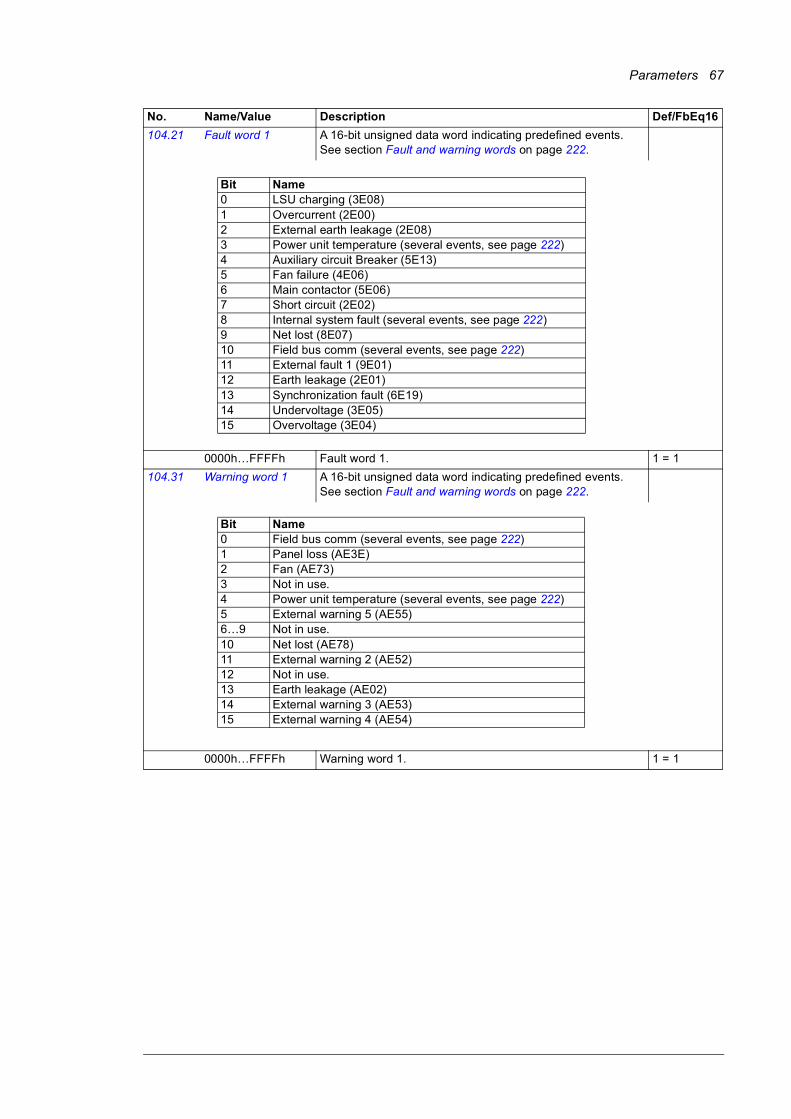
Parameters 67
104.21 Fault word 1 A 16-bit unsigned data word indicating predefined events. See section Fault and warning words on page 222.
0000h…FFFFh Fault word 1. 1 = 1
104.31 Warning word 1 A 16-bit unsigned data word indicating predefined events. See section Fault and warning words on page 222.
0000h…FFFFh Warning word 1. 1 = 1
No. Name/Value Description Def/FbEq16
Bit Name0 LSU charging (3E08)1 Overcurrent (2E00)2 External earth leakage (2E08)3 Power unit temperature (several events, see page 222)4 Auxiliary circuit Breaker (5E13)5 Fan failure (4E06)6 Main contactor (5E06)7 Short circuit (2E02)8 Internal system fault (several events, see page 222)9 Net lost (8E07)10 Field bus comm (several events, see page 222)11 External fault 1 (9E01)12 Earth leakage (2E01)13 Synchronization fault (6E19)14 Undervoltage (3E05)15 Overvoltage (3E04)
Bit Name0 Field bus comm (several events, see page 222)1 Panel loss (AE3E)2 Fan (AE73)3 Not in use.4 Power unit temperature (several events, see page 222)5 External warning 5 (AE55)6…9 Not in use.10 Net lost (AE78)11 External warning 2 (AE52)12 Not in use.13 Earth leakage (AE02)14 External warning 3 (AE53)15 External warning 4 (AE54)
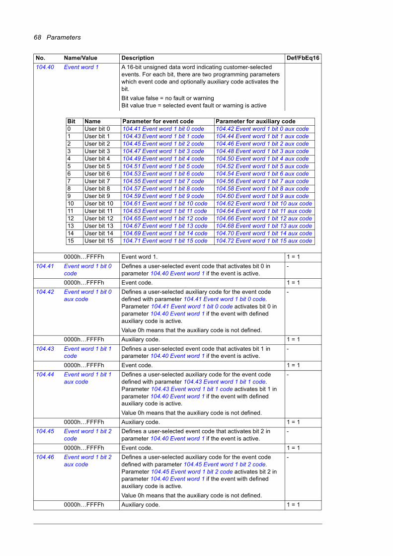
68 Parameters
104.40 Event word 1 A 16-bit unsigned data word indicating customer-selected events. For each bit, there are two programming parameters which event code and optionally auxiliary code activates the bit.
Bit value false = no fault or warningBit value true = selected event fault or warning is active
0000h…FFFFh Event word 1. 1 = 1
104.41 Event word 1 bit 0 code
Defines a user-selected event code that activates bit 0 in parameter 104.40 Event word 1 if the event is active.
-
0000h…FFFFh Event code. 1 = 1
104.42 Event word 1 bit 0 aux code
Defines a user-selected auxiliary code for the event code defined with parameter 104.41 Event word 1 bit 0 code. Parameter 104.41 Event word 1 bit 0 code activates bit 0 in parameter 104.40 Event word 1 if the event with defined auxiliary code is active.
Value 0h means that the auxiliary code is not defined.
-
0000h…FFFFh Auxiliary code. 1 = 1
104.43 Event word 1 bit 1 code
Defines a user-selected event code that activates bit 1 in parameter 104.40 Event word 1 if the event is active.
-
0000h…FFFFh Event code. 1 = 1
104.44 Event word 1 bit 1 aux code
Defines a user-selected auxiliary code for the event code defined with parameter 104.43 Event word 1 bit 1 code. Parameter 104.43 Event word 1 bit 1 code activates bit 1 in parameter 104.40 Event word 1 if the event with defined auxiliary code is active.
Value 0h means that the auxiliary code is not defined.
-
0000h…FFFFh Auxiliary code. 1 = 1
104.45 Event word 1 bit 2 code
Defines a user-selected event code that activates bit 2 in parameter 104.40 Event word 1 if the event is active.
-
0000h…FFFFh Event code. 1 = 1
104.46 Event word 1 bit 2 aux code
Defines a user-selected auxiliary code for the event code defined with parameter 104.45 Event word 1 bit 2 code. Parameter 104.45 Event word 1 bit 2 code activates bit 2 in parameter 104.40 Event word 1 if the event with defined auxiliary code is active.
Value 0h means that the auxiliary code is not defined.
-
0000h…FFFFh Auxiliary code. 1 = 1
No. Name/Value Description Def/FbEq16
Bit Name Parameter for event code Parameter for auxiliary code0 User bit 0 104.41 Event word 1 bit 0 code 104.42 Event word 1 bit 0 aux code1 User bit 1 104.43 Event word 1 bit 1 code 104.44 Event word 1 bit 1 aux code2 User bit 2 104.45 Event word 1 bit 2 code 104.46 Event word 1 bit 2 aux code3 User bit 3 104.47 Event word 1 bit 3 code 104.48 Event word 1 bit 3 aux code4 User bit 4 104.49 Event word 1 bit 4 code 104.50 Event word 1 bit 4 aux code5 User bit 5 104.51 Event word 1 bit 5 code 104.52 Event word 1 bit 5 aux code6 User bit 6 104.53 Event word 1 bit 6 code 104.54 Event word 1 bit 6 aux code7 User bit 7 104.55 Event word 1 bit 7 code 104.56 Event word 1 bit 7 aux code8 User bit 8 104.57 Event word 1 bit 8 code 104.58 Event word 1 bit 8 aux code9 User bit 9 104.59 Event word 1 bit 9 code 104.60 Event word 1 bit 9 aux code10 User bit 10 104.61 Event word 1 bit 10 code 104.62 Event word 1 bit 10 aux code11 User bit 11 104.63 Event word 1 bit 11 code 104.64 Event word 1 bit 11 aux code12 User bit 12 104.65 Event word 1 bit 12 code 104.66 Event word 1 bit 12 aux code13 User bit 13 104.67 Event word 1 bit 13 code 104.68 Event word 1 bit 13 aux code14 User bit 14 104.69 Event word 1 bit 14 code 104.70 Event word 1 bit 14 aux code15 User bit 15 104.71 Event word 1 bit 15 code 104.72 Event word 1 bit 15 aux code

Parameters 69
104.47 Event word 1 bit 3 code
Defines a user-selected event code that activates bit 3 in parameter 104.40 Event word 1 if the event is active.
-
0000h…FFFFh Event code. 1 = 1
104.48 Event word 1 bit 3 aux code
Defines a user-selected auxiliary code for the event code defined with parameter 104.47 Event word 1 bit 3 code. Parameter 104.47 Event word 1 bit 3 code activates bit 3 in parameter 104.40 Event word 1 if the event with defined auxiliary code is active.
Value 0h means that the auxiliary code is not defined.
-
0000h…FFFFh Auxiliary code. 1 = 1
104.49 Event word 1 bit 4 code
Defines a user-selected event code that activates bit 4 in parameter 104.40 Event word 1 if the event is active.
-
0000h…FFFFh Event code. 1 = 1
104.50 Event word 1 bit 4 aux code
Defines a user-selected auxiliary code for the event code defined with parameter 104.49 Event word 1 bit 4 code. Parameter 104.49 Event word 1 bit 4 code activates bit 4 in parameter 104.40 Event word 1 if the event with defined auxiliary code is active.
Value 0h means that the auxiliary code is not defined.
-
0000h…FFFFh Auxiliary code. 1 = 1
104.51 Event word 1 bit 5 code
Defines a user-selected event code that activates bit 5 in parameter 104.40 Event word 1 if the event is active.
-
0000h…FFFFh Event code. 1 = 1
104.52 Event word 1 bit 5 aux code
Defines a user-selected auxiliary code for the event code defined with parameter 104.51 Event word 1 bit 5 code. Parameter 104.51 Event word 1 bit 5 code activates bit 5 in parameter 104.40 Event word 1 if the event with defined auxiliary code is active.
Value 0h means that the auxiliary code is not defined.
-
0000h…FFFFh Auxiliary code. 1 = 1
104.53 Event word 1 bit 6 code
Defines a user-selected event code that activates bit 6 in parameter 104.40 Event word 1 if the event is active.
-
0000h…FFFFh Event code. 1 = 1
104.54 Event word 1 bit 6 aux code
Defines a user-selected auxiliary code for the event code defined with parameter 104.53 Event word 1 bit 6 code. Parameter 104.53 Event word 1 bit 6 code activates bit 6 in parameter 104.40 Event word 1 if the event with defined auxiliary code is active.
Value 0h means that the auxiliary code is not defined.
-
0000h…FFFFh Auxiliary code. 1 = 1
104.55 Event word 1 bit 7 code
Defines a user-selected event code that activates bit 7 in parameter 104.40 Event word 1 if the event is active.
-
0000h…FFFFh Event code. 1 = 1
104.56 Event word 1 bit 7 aux code
Defines a user-selected auxiliary code for the event code defined with parameter 104.55 Event word 1 bit 7 code. Parameter 104.55 Event word 1 bit 7 code activates bit 7 in parameter 104.40 Event word 1 if the event with defined auxiliary code is active.
Value 0h means that the auxiliary code is not defined.
-
0000h…FFFFh Auxiliary code. 1 = 1
104.57 Event word 1 bit 8 code
Defines a user-selected event code that activates bit 8 in parameter 104.40 Event word 1 if the event is active.
-
0000h…FFFFh Event code. 1 = 1
No. Name/Value Description Def/FbEq16

70 Parameters
104.58 Event word 1 bit 8 aux code
Defines a user-selected auxiliary code for the event code defined with parameter 104.57 Event word 1 bit 8 code. Parameter 104.57 Event word 1 bit 8 code activates bit 8 in parameter 104.40 Event word 1 if the event with defined auxiliary code is active.
Value 0h means that the auxiliary code is not defined.
-
0000h…FFFFh Auxiliary code. 1 = 1
104.59 Event word 1 bit 9 code
Defines a user-selected event code that activates bit 9 in parameter 104.40 Event word 1 if the event is active.
-
0000h…FFFFh Event code. 1 = 1
104.60 Event word 1 bit 9 aux code
Defines a user-selected auxiliary code for the event code defined with parameter 104.59 Event word 1 bit 9 code. Parameter 104.59 Event word 1 bit 9 code activates bit 9 in parameter 104.40 Event word 1 if the event with defined auxiliary code is active.
Value 0h means that the auxiliary code is not defined.
-
0000h…FFFFh Auxiliary code. 1 = 1
104.61 Event word 1 bit 10 code
Defines a user-selected event code that activates bit 10 in parameter 104.40 Event word 1 if the event is active.
-
0000h…FFFFh Event code. 1 = 1
104.62 Event word 1 bit 10 aux code
Defines a user-selected auxiliary code for the event code defined with parameter 104.61 Event word 1 bit 10 code. Parameter 104.61 Event word 1 bit 10 code activates bit 10 in parameter 104.40 Event word 1 if the event with defined auxiliary code is active.
Value 0h means that the auxiliary code is not defined.
-
0000h…FFFFh Auxiliary code. 1 = 1
104.63 Event word 1 bit 11 code
Defines a user-selected event code that activates bit 11 in parameter 104.40 Event word 1 if the event is active.
-
0000h…FFFFh Event code. 1 = 1
104.64 Event word 1 bit 11 aux code
Defines a user-selected auxiliary code for the event code defined with parameter 104.63 Event word 1 bit 11 code. Parameter 104.63 Event word 1 bit 11 code activates bit 11 in parameter 104.40 Event word 1 if the event with defined auxiliary code is active.
Value 0h means that the auxiliary code is not defined.
-
0000h…FFFFh Auxiliary code. 1 = 1
104.65 Event word 1 bit 12 code
Defines a user-selected event code that activates bit 12 in parameter 104.40 Event word 1 if the event is active.
-
0000h…FFFFh Event code. 1 = 1
104.66 Event word 1 bit 12 aux code
Defines a user-selected auxiliary code for the event code defined with parameter 104.65 Event word 1 bit 12 code. Parameter 104.65 Event word 1 bit 12 code activates bit 12 in parameter 104.40 Event word 1 if the event with defined auxiliary code is active.
Value 0h means that the auxiliary code is not defined.
-
0000h…FFFFh Auxiliary code. 1 = 1
104.67 Event word 1 bit 13 code
Defines a user-selected event code that activates bit 13 in parameter 104.40 Event word 1 if the event is active.
-
0000h…FFFFh Event code. 1 = 1
No. Name/Value Description Def/FbEq16

Parameters 71
104.68 Event word 1 bit 13 aux code
Defines a user-selected auxiliary code for the event code defined with parameter 104.67 Event word 1 bit 13 code. Parameter 104.67 Event word 1 bit 13 code activates bit 13 in parameter 104.40 Event word 1 if the event with defined auxiliary code is active.
Value 0h means that the auxiliary code is not defined.
-
0000h…FFFFh Auxiliary code. 1 = 1
104.69 Event word 1 bit 14 code
Defines a user-selected event code that activates bit 14 in parameter 104.40 Event word 1 if the event is active.
-
0000h…FFFFh Event code. 1 = 1
104.70 Event word 1 bit 14 aux code
Defines a user-selected auxiliary code for the event code defined with parameter 104.69 Event word 1 bit 14 code. Parameter 104.69 Event word 1 bit 14 code activates bit 14 in parameter 104.40 Event word 1 if the event with defined auxiliary code is active.
Value 0h means that the auxiliary code is not defined.
-
0000h…FFFFh Auxiliary code. 1 = 1
104.71 Event word 1 bit 15 code
Defines a user-selected event code that activates bit 15 in parameter 104.40 Event word 1 if the event is active.
-
0000h…FFFFh Event code. 1 = 1
104.72 Event word 1 bit 15 aux code
Defines a user-selected auxiliary code for the event code defined with parameter 104.71 Event word 1 bit 15 code. Parameter 104.71 Event word 1 bit 15 code activates bit 15 in parameter 104.40 Event word 1 if the event with defined auxiliary code is active.
Value 0h means that the auxiliary code is not defined.
-
0000h…FFFFh Auxiliary code. 1 = 1
105105 Diagnostics Various run-time-type counters and measurements related to
IGBT supply unit maintenance.All parameters in this group are read-only unless otherwise noted.
105.01 On-time counter On-time counter. The counter runs when the IGBT supply unit is powered.
-
0…65535 d On-time counter. 1 = 1 d
105.02 Run-time counter Run-time counter. The counter runs when the IGBT supply unit modulates.
-
0…65535 d Run-time counter. 1 = 1 d
105.04 Fan on-time counter Running time of the cooling fan. Can be reset on the control panel by keeping Reset depressed for over 3 seconds.
-
0…65535 d Cooling fan run-time counter. 1 = 1 d
105.09 Time from power-up 500-microsecond ticks elapsed since the last boot of the control unit.
-
0…4294967295 500-microsecond ticks since last boot. 1 = 1
105.11 Converter temperature %
Converter temperature in percent of the fault limit. -
-40.0 … 160.0% Converter temperature in percent. 1 = 1%
105.21 MCB closing time counter
Counts the closures of the main circuit breaker (MCB). This parameter can be used for maintenance purposes. Depending on application, the maintenance interval of the main circuit breaker may vary. See the maintenance instructions of the main circuit breaker.
-
0…4294967295 Count of closures of main circuit breaker. 1 = 1
No. Name/Value Description Def/FbEq16
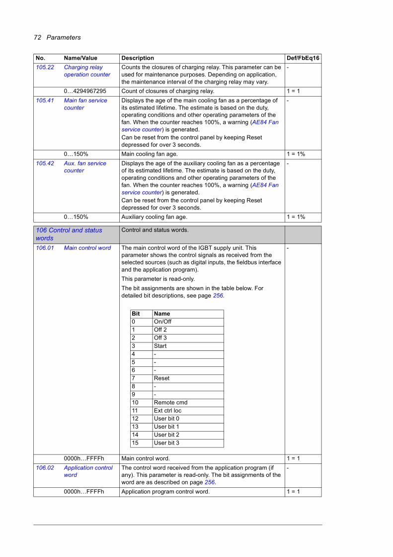
72 Parameters
105.22 Charging relay operation counter
Counts the closures of charging relay. This parameter can be used for maintenance purposes. Depending on application, the maintenance interval of the charging relay may vary.
-
0…4294967295 Count of closures of charging relay. 1 = 1
105.41 Main fan service counter
Displays the age of the main cooling fan as a percentage of its estimated lifetime. The estimate is based on the duty, operating conditions and other operating parameters of the fan. When the counter reaches 100%, a warning (AE84 Fan service counter) is generated.Can be reset from the control panel by keeping Reset depressed for over 3 seconds.
-
0…150% Main cooling fan age. 1 = 1%
105.42 Aux. fan service counter
Displays the age of the auxiliary cooling fan as a percentage of its estimated lifetime. The estimate is based on the duty, operating conditions and other operating parameters of the fan. When the counter reaches 100%, a warning (AE84 Fan service counter) is generated.Can be reset from the control panel by keeping Reset depressed for over 3 seconds.
-
0…150% Auxiliary cooling fan age. 1 = 1%
106106 Control and status words
Control and status words.
106.01 Main control word The main control word of the IGBT supply unit. This parameter shows the control signals as received from the selected sources (such as digital inputs, the fieldbus interface and the application program).
This parameter is read-only.
The bit assignments are shown in the table below. For detailed bit descriptions, see page 256.
-
0000h…FFFFh Main control word. 1 = 1
106.02 Application control word
The control word received from the application program (if any). This parameter is read-only. The bit assignments of the word are as described on page 256.
-
0000h…FFFFh Application program control word. 1 = 1
No. Name/Value Description Def/FbEq16
Bit Name0 On/Off1 Off 22 Off 33 Start4 -5 -6 -7 Reset8 -9 -10 Remote cmd11 Ext ctrl loc12 User bit 013 User bit 114 User bit 215 User bit 3

Parameters 73
106.03 FBA A transparent control word
The control word from fieldbus A, when transparent profile is used.
-
0…4294967295 The control word from fieldbus A. 1 = 1
106.04 FBA B transparent control word
Displays the unaltered control word received from the PLC through fieldbus adapter B when a transparent communication profile is selected eg. by parameter group 154 FBA B settings. See section Control word and Status word (page 253).This parameter is read-only.
-
00000000h … FFFFFFFFh
Control word received through fieldbus adapter B. 1 = 1
106.11 Main status word Main status word of the IGBT supply unit.
This parameter is read-only.
The bit assignments are shown in the table below. For detailed bit descriptions, see page 257.
-
0000h…FFFFh Main status word. 1 = 1
106.16 Drive status word 1 Drive status word 1.
This parameter is read-only.
-
0000h…FFFFh Drive status word 1. 1 = 1
No. Name/Value Description Def/FbEq16
Bit Name0 Ready to switch ON1 Ready run2 Ready ref3 Tripped4 -5 -6 -7 Warning8 Modulating9 Remote10 Net OK11 User bit 012 User bit 113 User bit 214 Charging15 User bit 3
Bit Name Description0 Enabled 1 = Run enable and start enable signals are present1 Inhibited 1 = Start inhibited2 Operation allowed 1 = Drive is ready to operate3 Ready to start 1 = Drive is ready to receive a start command4 Running 1 = Drive is ready to follow given reference5 Started 1 = Drive has been started6 Modulating 1 = Drive is modulating (output stage is being controlled)7 Limiting 1 = Any operating limit is active8 Local control 1 = Drive is in local control9 Network control 1 = Drive is in network control10 Ext1 active 1 = Control location Ext1 active11 Ext2 active 1 = Control location Ext2 active12 Charging relay 1 = Charging relay is closed13 MCB relay 1 = MCB relay is closed14…15 Reserved

74 Parameters
106.17 Drive status word 2 Drive status word 2.
This parameter is read-only.
-
0000h…FFFFh Drive status word 2. 1 = 1
106.18 Start inhibit status word
Start inhibit status word. -
0000h…FFFFh Start inhibit status word. 1 = 1
No. Name/Value Description Def/FbEq16
Bit Name Description0 Start req final1 Reserved2 Reserved3 Reserved4 Power control Power control.5 Internal UDC reference When the bit is set, the drive is not able to fulfill user
reference and follows its internally calculated reference. The bits are updated only when the drive is modulating.
6 Internal power reference7 Internal reactive power
reference8 Reserved9 Reserved10 Reserved11 Emergency stop active 1 = An emergency stop command signal is active, or
the drive is stopping after receiving an emergency stop command.
12 Reduced run 1 = Reduced run active (see section Reduced run function on page 32)
13…15 Reserved
Bit Name0 Not ready run1 Ctrl location changed2 SSW inhibit3 Fault4 Lost start enable5 Lost run enable6 Reserved7 Reserved8 Reserved9 Charging overload10 Reserved11 Reserved12 Em Off213 Em Off314 Auto reset inhibit15 Off grid configuration
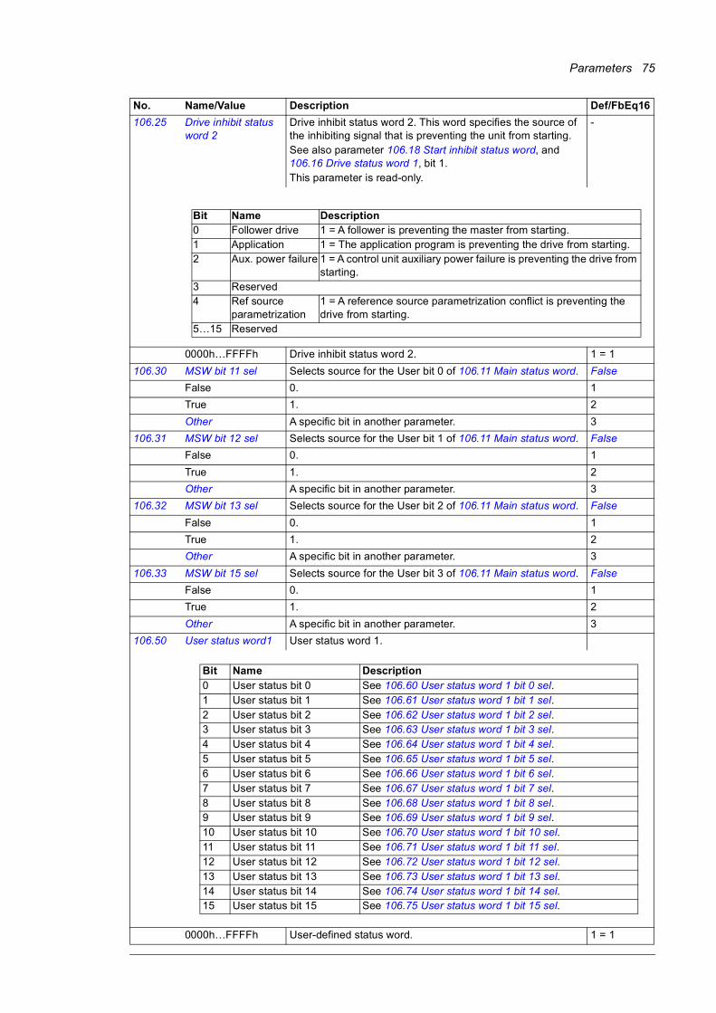
Parameters 75
106.25 Drive inhibit status word 2
Drive inhibit status word 2. This word specifies the source of the inhibiting signal that is preventing the unit from starting.See also parameter 106.18 Start inhibit status word, and 106.16 Drive status word 1, bit 1.This parameter is read-only.
-
0000h…FFFFh Drive inhibit status word 2. 1 = 1
106.30 MSW bit 11 sel Selects source for the User bit 0 of 106.11 Main status word. False
False 0. 1
True 1. 2
Other A specific bit in another parameter. 3
106.31 MSW bit 12 sel Selects source for the User bit 1 of 106.11 Main status word. False
False 0. 1
True 1. 2
Other A specific bit in another parameter. 3
106.32 MSW bit 13 sel Selects source for the User bit 2 of 106.11 Main status word. False
False 0. 1
True 1. 2
Other A specific bit in another parameter. 3
106.33 MSW bit 15 sel Selects source for the User bit 3 of 106.11 Main status word. False
False 0. 1
True 1. 2
Other A specific bit in another parameter. 3
106.50 User status word1 User status word 1.
0000h…FFFFh User-defined status word. 1 = 1
No. Name/Value Description Def/FbEq16
Bit Name Description0 Follower drive 1 = A follower is preventing the master from starting.1 Application 1 = The application program is preventing the drive from starting.2 Aux. power failure 1 = A control unit auxiliary power failure is preventing the drive from
starting.3 Reserved4 Ref source
parametrization1 = A reference source parametrization conflict is preventing the drive from starting.
5…15 Reserved
Bit Name Description0 User status bit 0 See 106.60 User status word 1 bit 0 sel.1 User status bit 1 See 106.61 User status word 1 bit 1 sel.2 User status bit 2 See 106.62 User status word 1 bit 2 sel.3 User status bit 3 See 106.63 User status word 1 bit 3 sel.4 User status bit 4 See 106.64 User status word 1 bit 4 sel.5 User status bit 5 See 106.65 User status word 1 bit 5 sel.6 User status bit 6 See 106.66 User status word 1 bit 6 sel.7 User status bit 7 See 106.67 User status word 1 bit 7 sel.8 User status bit 8 See 106.68 User status word 1 bit 8 sel.9 User status bit 9 See 106.69 User status word 1 bit 9 sel.10 User status bit 10 See 106.70 User status word 1 bit 10 sel.11 User status bit 11 See 106.71 User status word 1 bit 11 sel.12 User status bit 12 See 106.72 User status word 1 bit 12 sel.13 User status bit 13 See 106.73 User status word 1 bit 13 sel.14 User status bit 14 See 106.74 User status word 1 bit 14 sel.15 User status bit 15 See 106.75 User status word 1 bit 15 sel.
76 Parameters
106.60 User status word 1 bit 0 sel
Selects a binary source whose status is transmitted as bit 0 of 106.50 User status word1.
False
False 0. 1
True 1. 2
Other A specific bit in another parameter. 3
106.61 User status word 1 bit 1 sel
Selects a binary source whose status is transmitted as bit 1 of 106.50 User status word1.
False
False 0. 1
True 1. 2
Other A specific bit in another parameter. 3
106.62 User status word 1 bit 2 sel
Selects a binary source whose status is transmitted as bit 2 of 106.50 User status word1.
False
False 0. 1
True 1. 2
Other A specific bit in another parameter. 3
106.63 User status word 1 bit 3 sel
Selects a binary source whose status is transmitted as bit 3 of 106.50 User status word1.
False
False 0. 1
True 1. 2
Other A specific bit in another parameter. 3
106.64 User status word 1 bit 4 sel
Selects a binary source whose status is transmitted as bit 4 of 106.50 User status word1.
False
False 0. 1
True 1. 2
Other A specific bit in another parameter. 3
106.65 User status word 1 bit 5 sel
Selects a binary source whose status is transmitted as bit 5 of 106.50 User status word1.
False
False 0. 1
True 1. 2
Other A specific bit in another parameter. 3
106.66 User status word 1 bit 6 sel
Selects a binary source whose status is transmitted as bit 6 of 106.50 User status word1.
False
False 0. 1
True 1. 2
Other A specific bit in another parameter. 3
106.67 User status word 1 bit 7 sel
Selects a binary source whose status is transmitted as bit 7 of 106.50 User status word1.
False
False 0. 1
True 1. 2
Other A specific bit in another parameter. 3
106.68 User status word 1 bit 8 sel
Selects a binary source whose status is transmitted as bit 8 of 106.50 User status word1.
False
False 0. 1
True 1. 2
Other A specific bit in another parameter. 3
106.69 User status word 1 bit 9 sel
Selects a binary source whose status is transmitted as bit 9 of 106.50 User status word1.
False
False 0. 1
True 1. 2
Other A specific bit in another parameter. 3
No. Name/Value Description Def/FbEq16
Parameters 77
106.70 User status word 1 bit 10 sel
Selects a binary source whose status is transmitted as bit 10 of 106.50 User status word1.
False
False 0. 1
True 1. 2
Other A specific bit in another parameter. 3
106.71 User status word 1 bit 11 sel
Selects a binary source whose status is transmitted as bit 11 of 106.50 User status word1.
False
False 0. 1
True 1. 2
Other A specific bit in another parameter. 3
106.72 User status word 1 bit 12 sel
Selects a binary source whose status is transmitted as bit 12 of 106.50 User status word1.
False
False 0. 1
True 1. 2
Other A specific bit in another parameter. 3
106.73 User status word 1 bit 13 sel
Selects a binary source whose status is transmitted as bit 13 of 106.50 User status word1.
False
False 0. 1
True 1. 2
Other A specific bit in another parameter. 3
106.74 User status word 1 bit 14 sel
Selects a binary source whose status is transmitted as bit 14 of 106.50 User status word1.
False
False 0. 1
True 1. 2
Other A specific bit in another parameter. 3
106.75 User status word 1 bit 15 sel
Selects a binary source whose status is transmitted as bit 15 of 106.50 User status word1.
False
False 0. 1
True 1. 2
Other A specific bit in another parameter. 3
106.100 User control word 1 User-defined control word 1.
0000h…FFFFh User-defined control word 1. 1 = 1
No. Name/Value Description Def/FbEq16
Bit Name0 User control word 1 bit 0 sel1 User control word 1 bit 1 sel2 User control word 1 bit 2 sel3 User control word 1 bit 3 sel4 User control word 1 bit 4 sel5 User control word 1 bit 5 sel6 User control word 1 bit 6 sel7 User control word 1 bit 7 sel8 User control word 1 bit 8 sel9 User control word 1 bit 9 sel10 User control word 1 bit 10 sel11 User control word 1 bit 11 sel12 User control word 1 bit 12 sel13 User control word 1 bit 13 sel14 User control word 1 bit 14 sel15 User control word 1 bit 15 sel
78 Parameters
106.101 User control word 2 User-defined control word 2.
0000h…FFFFh User-defined control word 2. 1 = 1
107107 System info Hardware and firmware information.
All parameters in this group are read-only.
107.03 Drive rating id Type of the unit. -
0…999 Type of the unit. -
107.04 Firmware name Firmware identification. -
107.05 Firmware version Version number of the firmware. -
107.06 Loading package name
Name of the firmware loading package. -
107.07 Loading package version
Version number of the firmware loading package. -
107.08 Bootloader version Version number of the firmware bootloader. -
107.11 Cpu usage Microprocessor load in percent. -
0…100% Microprocessor load. 1 = 1%
107.13 PU logic version number
The version number of the power unit FPGA logic. -
107.23 Application name First five ASCII letters of the name given to the application program in the programming tool. The full name is visible under System info on the control panel or the Drive composer PC tool._N/A_ = None.
-
107.24 Application version Application program version number given to the application program in the programming tool. Also visible under System info on the control panel or the Drive composer PC tool.
-
107.25 Customization package name
First five ASCII letters of the name given to the customization package. The full name is visible under System info on the control panel or the Drive composer PC tool._N/A_ = None.
-
107.26 Customization package version
Customization package version number. Also visible under System info on the control panel or the Drive composer PC tool.
-
No. Name/Value Description Def/FbEq16
Bit Name0 User control word 2 bit 0 sel1 User control word 2 bit 1 sel2 User control word 2 bit 2 sel3 User control word 2 bit 3 sel4 User control word 2 bit 4 sel5 User control word 2 bit 5 sel6 User control word 2 bit 6 sel7 User control word 2 bit 7 sel8 User control word 2 bit 8 sel9 User control word 2 bit 9 sel10 User control word 2 bit 10 sel11 User control word 2 bit 11 sel12 User control word 2 bit 12 sel13 User control word 2 bit 13 sel14 User control word 2 bit 14 sel15 User control word 2 bit 15 sel
Parameters 79
107.30 Adaptive program status
Shows the status of the adaptive program.See section Adaptive programming (page 23).
-
0000h…FFFFh Adaptive program status. 1 = 1
110110 Standard DI, RO Configuration of digital inputs and relay outputs.
110.01 DI status Displays the electrical status of digital inputs DIIL and DI6…DI1. The activation/deactivation delays of the inputs (if any are specified) are ignored.
Bits 0…5 reflect the status of DI1…DI6; bit 15 reflects the status of the DIIL input.
This parameter is read-only.
-
0000h…FFFFh Status of digital inputs. 1 = 1
110.02 DI delayed status Displays the status of digital inputs DIIL and DI6…DI1. This word is updated only after activation/deactivation delays.
Bits 0…5 reflect the delayed status of DI1…DI6; bit 15 reflects the delayed status of the DIIL input.
This parameter is read-only.
-
0000h…FFFFh Delayed status of digital inputs. 1 = 1
110.03 DI force selection Selects if the electrical statuses of digital inputs will be overridden by bits on signal 110.04 DI force data. These values overrides the electrical statuses of the digital inputs in eg. testing purposes. A bit in parameter 110.04 DI force data is provided for each digital input, and its value is applied whenever the corresponding bit in this parameter is 1.
0000h
0000h…FFFFh Override selection for digital inputs. 1 = 1
110.04 DI force data Defines the values of digital inputs that are used instead of the electrical statuses if selected in parameter 110.03 DI force selection. Bit 0 is the forced value for DI1; bit 15 is the forced value for the DIIL input.
0000h
0000h…FFFFh Forced values of digital inputs. 1 = 1
No. Name/Value Description Def/FbEq16
Bit Name Description0 Initialized 1 = Adaptive program initialized1 Editing 1 = Adaptive program is being edited2 Edit done 1 = Editing of adaptive program finished3 Running 1 = Adaptive program running4…13 Reserved14 State changing Reserved15 Faulted 1 = Error in adaptive program
Bit Value0 1 = Force DI1 to value of bit 0 of parameter 110.04 DI force data.1 1 = Force DI2 to value of bit 1 of parameter 110.04 DI force data.2 1 = Force DI3 to value of bit 2 of parameter 110.04 DI force data.3 1 = Force DI4 to value of bit 3 of parameter 110.04 DI force data.4 1 = Force DI5 to value of bit 4 of parameter 110.04 DI force data.5 1 = Force DI6 to value of bit 5 of parameter 110.04 DI force data.6…14 Reserved15 1 = Force DIIL to value of bit 15 of parameter 110.04 DI force data.

80 Parameters
110.05 DI1 ON delay Defines the activation delay for digital input DI1. 0.0 s
tOn = 110.05 DI1 ON delay
tOff = 110.06 DI1 OFF delay
*Electrical status of digital input. Indicated by 110.01 DI status.**Indicated by 110.02 DI delayed status.
0.0 … 3000.0 s Activation delay for DI1. 10 = 1 s
110.06 DI1 OFF delay Defines the deactivation delay for digital input DI1. See parameter 110.05 DI1 ON delay.
0.0 s
0.0 … 3000.0 s Deactivation delay for DI1. 10 = 1 s
110.07 DI2 ON delay Defines the activation delay for digital input DI2. 0.0 s
tOn = 110.07 DI2 ON delay
tOff = 110.08 DI2 OFF delay
*Electrical status of digital input. Indicated by 110.01 DI status.**Indicated by 110.02 DI delayed status.
0.0 … 3000.0 s Activation delay for DI2. 10 = 1 s
110.08 DI2 OFF delay Defines the deactivation delay for digital input DI2. See parameter 110.07 DI2 ON delay.
0.0 s
0.0 … 3000.0 s Deactivation delay for DI2. 10 = 1 s
110.09 DI3 ON delay Defines the activation delay for digital input DI3. 0.0 s
tOn = 110.09 DI3 ON delay
tOff = 110.10 DI3 OFF delay
*Electrical status of digital input. Indicated by 110.01 DI status.**Indicated by 110.02 DI delayed status.
0.0 … 3000.0 s Activation delay for DI3. 10 = 1 s
110.10 DI3 OFF delay Defines the deactivation delay for digital input DI3. See parameter 110.09 DI3 ON delay.
0.0 s
0.0 … 3000.0 s Deactivation delay for DI3. 10 = 1 s
No. Name/Value Description Def/FbEq16
1
0
1
0
tOn tOff tOn tOff
*DI status
**Delayed DI status
Time
1
0
1
0
tOn tOff tOn tOff
*DI status
**Delayed DI status
Time
1
0
1
0
tOn tOff tOn tOff
*DI status
**Delayed DI status
Time
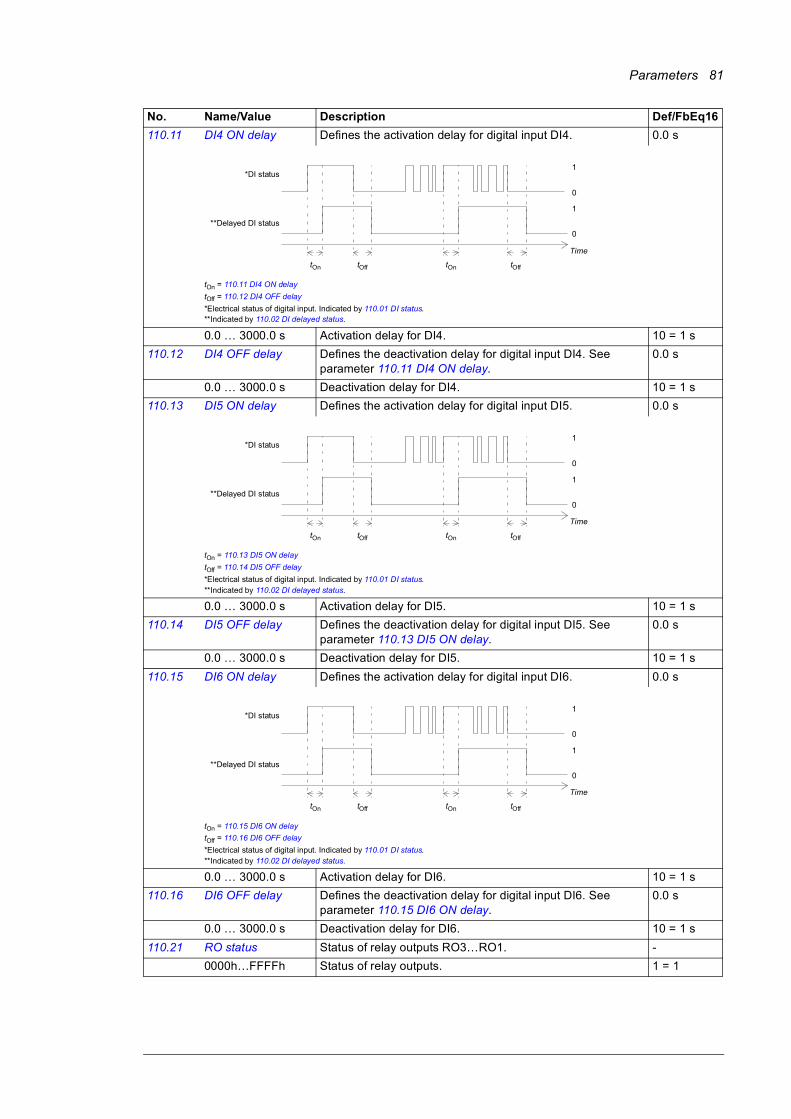
Parameters 81
110.11 DI4 ON delay Defines the activation delay for digital input DI4. 0.0 s
tOn = 110.11 DI4 ON delay
tOff = 110.12 DI4 OFF delay
*Electrical status of digital input. Indicated by 110.01 DI status.**Indicated by 110.02 DI delayed status.
0.0 … 3000.0 s Activation delay for DI4. 10 = 1 s
110.12 DI4 OFF delay Defines the deactivation delay for digital input DI4. See parameter 110.11 DI4 ON delay.
0.0 s
0.0 … 3000.0 s Deactivation delay for DI4. 10 = 1 s
110.13 DI5 ON delay Defines the activation delay for digital input DI5. 0.0 s
tOn = 110.13 DI5 ON delay
tOff = 110.14 DI5 OFF delay
*Electrical status of digital input. Indicated by 110.01 DI status.**Indicated by 110.02 DI delayed status.
0.0 … 3000.0 s Activation delay for DI5. 10 = 1 s
110.14 DI5 OFF delay Defines the deactivation delay for digital input DI5. See parameter 110.13 DI5 ON delay.
0.0 s
0.0 … 3000.0 s Deactivation delay for DI5. 10 = 1 s
110.15 DI6 ON delay Defines the activation delay for digital input DI6. 0.0 s
tOn = 110.15 DI6 ON delay
tOff = 110.16 DI6 OFF delay
*Electrical status of digital input. Indicated by 110.01 DI status.**Indicated by 110.02 DI delayed status.
0.0 … 3000.0 s Activation delay for DI6. 10 = 1 s
110.16 DI6 OFF delay Defines the deactivation delay for digital input DI6. See parameter 110.15 DI6 ON delay.
0.0 s
0.0 … 3000.0 s Deactivation delay for DI6. 10 = 1 s
110.21 RO status Status of relay outputs RO3…RO1. -
0000h…FFFFh Status of relay outputs. 1 = 1
No. Name/Value Description Def/FbEq16
1
0
1
0
tOn tOff tOn tOff
*DI status
**Delayed DI status
Time
1
0
1
0
tOn tOff tOn tOff
*DI status
**Delayed DI status
Time
1
0
1
0
tOn tOff tOn tOff
*DI status
**Delayed DI status
Time

82 Parameters
110.24 RO1 source Selects a signal to be connected to relay output RO1.
Note: This parameter is write-protected if parameter 120.30 External charge enable is set to Yes.
Charging
Not energized Relay output is not energized. 0
Energized Relay output is energized. 1
Ready Bit 0 of 106.11 Main status word (see page 73). Relay is energized when the IGBT supply unit is ready.
2
Enabled Bit 0 of 106.16 Drive status word 1 (see page 73). Relay is energized when the IGBT supply unit is enabled.
3
Started Bit 5 of 106.16 Drive status word 1 (see page 73). Relay is energized when the IGBT supply unit is started.
4
Running Bit 4 of 106.16 Drive status word 1 (see page 73). Relay is energized when the IGBT supply unit is running.
5
Warning Bit 7 of 106.11 Main status word (see page 73). Relay is energized when a warning is active.
6
Fault Bit 3 of 106.11 Main status word (see page 73). Relay is energized when a fault is active.
7
Fault (-1) Inverted bit 3 of 106.11 Main status word (see page 73). 8
MCB Bit 13 of 106.16 Drive status word 1 (see page 73). Relay is energized when MCB closing command is given.
9
Charging Bit 12 of 106.16 Drive status word 1 (see page 73). Relay is energized when the external charging has charged the IGBT supply unit.
10
Start req final Bit 0 of 106.17 Drive status word 2 (see page 74). 11
Other A specific bit in another parameter. -
110.25 RO1 ON delay Defines the activation delay for relay output RO1. 0.0 s
tOn = 110.25 RO1 ON delay
tOff = 110.26 RO1 OFF delay
0.0 … 3000.0 s Activation delay for RO1. 10 = 1 s
110.26 RO1 OFF delay Defines the deactivation delay for relay output RO1. See parameter 110.25 RO1 ON delay.
0.0 s
0.0 … 3000.0 s Deactivation delay for RO1. 10 = 1 s
110.27 RO2 source Selects a signal to be connected to relay output RO2.
For the selections, see parameter 110.24 RO1 source.
Fault (-1)
110.28 RO2 ON delay Defines the activation delay for relay output RO2. 0.0 s
tOn = 110.28 RO2 ON delay
tOff = 110.29 RO2 OFF delay
0.0 … 3000.0 s Activation delay for RO2. 10 = 1 s
No. Name/Value Description Def/FbEq16
1
0
1
0
tOn tOff tOn tOff
Status of selectedsource
RO status
Time
1
0
1
0
tOn tOff tOn tOff
Status of selectedsource
RO status
Time
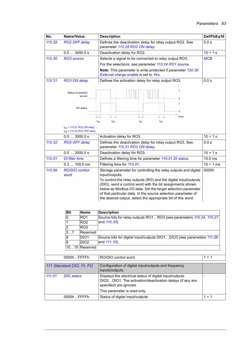
Parameters 83
110.29 RO2 OFF delay Defines the deactivation delay for relay output RO2. See parameter 110.28 RO2 ON delay.
0.0 s
0.0 … 3000.0 s Deactivation delay for RO2. 10 = 1 s
110.30 RO3 source Selects a signal to be connected to relay output RO3.
For the selections, see parameter 110.24 RO1 source.
Note: This parameter is write-protected if parameter 120.30 External charge enable is set to Yes.
MCB
110.31 RO3 ON delay Defines the activation delay for relay output RO3. 0.0 s
tOn = 110.31 RO3 ON delay
tOff = 110.32 RO3 OFF delay
0.0 … 3000.0 s Activation delay for RO3. 10 = 1 s
110.32 RO3 OFF delay Defines the deactivation delay for relay output RO3. See parameter 110.31 RO3 ON delay.
0.0 s
0.0 … 3000.0 s Deactivation delay for RO3. 10 = 1 s
110.51 DI filter time Defines a filtering time for parameter 110.01 DI status. 10.0 ms
0.3 … 100.0 ms Filtering time for 110.01. 10 = 1 ms
110.99 RO/DIO control word
Storage parameter for controlling the relay outputs and digital input/outputs.To control the relay outputs (RO) and the digital input/outputs (DIO), send a control word with the bit assignments shown below as Modbus I/O data. Set the target selection parameter of that particular data. In the source selection parameter of the desired output, select the appropriate bit of this word.
0000h
0000h…FFFFh RO/DIO control word. 1 = 1
111111 Standard DIO, FI, FO Configuration of digital input/outputs and frequency
inputs/outputs.
111.01 DIO status Displays the electrical status of digital input/outputs DIO2…DIO1. The activation/deactivation delays (if any are specified) are ignored.
This parameter is read-only.
-
0000h…FFFFh Status of digital input/outputs. 1 = 1
No. Name/Value Description Def/FbEq16
1
0
1
0
tOn tOff tOn tOff
Status of selectedsource
RO status
Time
Bit Name Description0 RO1 Source bits for relay outputs RO1…RO3 (see parameters 110.24, 110.27
and 110.30).1 RO22 RO33…7 Reserved8 DIO1 Source bits for digital input/outputs DIO1…DIO3 (see parameters 111.06
and 111.10).9 DIO210…15 Reserved

84 Parameters
111.02 DIO delayed status Displays the status of digital input/outputs DIO2…DIO1. This word is updated only after activation/deactivation (if any) delays.
This parameter is read-only.
-
0000h…FFFFh Delayed status of digital input/outputs. 1 = 1
111.05 DIO1 function Selects whether DIO1 is used as a digital output or input, or a frequency input.
Output
Output DIO1 is used as a digital output. 0
Input DIO1 is used as a digital input. 1
Frequency DIO1 is used as a frequency input. 2
111.06 DIO1 output source Selects a signal to be connected to digital input/output DIO1 when parameter 111.05 DIO1 function is set to Output.
Charging
Not energized Output is not energized. 0
Energized Output is energized. 1
Ready Bit 0 of 106.11 Main status word (see page 73). Output is energized when the IGBT supply unit is ready.
2
Charge ready Bit 1 of 106.11 Main status word (see page 73). Output is energized when the intermediate circuit DC charging is ready.
3
Enabled Bit 0 of 106.16 Drive status word 1 (see page 73). Output is energized when the IGBT supply unit is enabled.
4
Started Bit 5 of 106.16 Drive status word 1 (see page 73). Output is energized when the IGBT supply unit is started.
5
Running Bit 4 of 106.16 Drive status word 1 (see page 73). Output is energized when the IGBT supply unit is running.
6
Warning Bit 7 of 106.11 Main status word (see page 73). Output is energized when a warning is active.
7
Fault Bit 3 of 106.11 Main status word (see page 73). Output is energized when a fault is active.
8
MCB Bit 13 of 106.16 Drive status word 1 (see page 73). Output is energized when MCB closing command is given.
9
Charging Bit 12 of 106.16 Drive status word 1 (see page 73). Output is energized when the external charging has charged the IGBT supply unit.
10
Start req final Bit 0 of 106.17 Drive status word 2 (see page 74). 11
Other A specific bit in another parameter. -
111.07 DIO1 ON delay Defines the activation delay for digital input/output DIO1 (when used as a digital output or digital input).
0.0 s
tOn = 111.07 DIO1 ON delay
tOff = 111.08 DIO1 OFF delay
*Electrical status of DIO (in input mode) or status of selected source (in output mode). Indicated by 111.01 DIO status.**Indicated by 111.02 DIO delayed status.
0.0 … 3000.0 s Activation delay for DIO1. 10 = 1 s
111.08 DIO1 OFF delay Defines the deactivation delay for digital input/output DIO1 (when used as a digital output or digital input). See parameter 111.07 DIO1 ON delay.
0.0 s
0.0 … 3000.0 s Deactivation delay for DIO1. 10 = 1 s
No. Name/Value Description Def/FbEq16
1
0
1
0
tOn tOff tOn tOff
*DIO status
**Delayed DIO status
Time

Parameters 85
111.09 DIO2 function Selects whether DIO2 is used as a digital output or input, or a frequency output.
Output
Output DIO2 is used as a digital output. 0
Input DIO2 is used as a digital input. 1
111.10 DIO2 output source Selects a signal to be connected to digital input/output DIO2 when parameter 111.09 DIO2 function is set to Output. For selections, see parameter 111.06 DIO1 output source.
MCB
111.11 DIO2 ON delay Defines the activation delay for digital input/output DIO2 (when used as a digital output or digital input).
0.0 s
tOn = 111.11 DIO2 ON delay
tOff = 111.12 DIO2 OFF delay
*Electrical status of DIO (in input mode) or status of selected source (in output mode). Indicated by 111.01 DIO status.**Indicated by 111.02 DIO delayed status.
0.0 … 3000.0 s Activation delay for DIO2. 10 = 1 s
111.12 DIO2 OFF delay Defines the deactivation delay for digital input/output DIO2 (when used as a digital output or digital input). See parameter 111.11 DIO2 ON delay.
0.0 s
0.0 … 3000.0 s Deactivation delay for DIO2. 10 = 1 s
111.38 Freq in 1 actual value
Displays the value of frequency input 1 before scaling. See parameter 111.42 Freq in 1 min.
This parameter is read-only.
-
0 … 16000 Hz Unscaled value of frequency input 1. 1 = 1 Hz
111.39 Freq in 1 scaled Displays the value of frequency input 1 after scaling. See parameter 111.42 Freq in 1 min.
This parameter is read-only.
-
-32768.000 … 32767.000
Scaled value of frequency input 1. 1 = 1
111.42 Freq in 1 min Defines the minimum input frequency for frequency input 1 (DIO1 when it is used as a frequency input).
The incoming frequency signal (111.38 Freq in 1 actual value) is scaled into an internal signal (111.39 Freq in 1 scaled) by parameters 111.42…111.45 as follows:
0 Hz
0 … 16000 Hz Minimum frequency of frequency input 1 (DIO1). 1 = 1 Hz
No. Name/Value Description Def/FbEq16
1
0
1
0
tOn tOff tOn tOff
*DIO status
**Delayed DIO status
Time
111.43
111.45
111.42
111.39
111.38
111.44
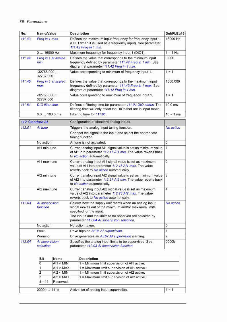
86 Parameters
111.43 Freq in 1 max Defines the maximum input frequency for frequency input 1 (DIO1 when it is used as a frequency input). See parameter 111.42 Freq in 1 min.
16000 Hz
0 … 16000 Hz Maximum frequency for frequency input 1 (DIO1). 1 = 1 Hz
111.44 Freq in 1 at scaled min
Defines the value that corresponds to the minimum input frequency defined by parameter 111.42 Freq in 1 min. See diagram at parameter 111.42 Freq in 1 min.
0.000
-32768.000 … 32767.000
Value corresponding to minimum of frequency input 1. 1 = 1
111.45 Freq in 1 at scaled max
Defines the value that corresponds to the maximum input frequency defined by parameter 111.43 Freq in 1 max. See diagram at parameter 111.42 Freq in 1 min.
1500.000
-32768.000 … 32767.000
Value corresponding to maximum of frequency input 1. 1 = 1
111.81 DIO filter time Defines a filtering time for parameter 111.01 DIO status. The filtering time will only affect the DIOs that are in input mode.
10.0 ms
0.3 … 100.0 ms Filtering time for 111.01. 10 = 1 ms
112112 Standard AI Configuration of standard analog inputs.
112.01 AI tune Triggers the analog input tuning function.
Connect the signal to the input and select the appropriate tuning function.
No action
No action AI tune is not activated. 0
AI1 min tune Current analog input AI1 signal value is set as minimum value of AI1 into parameter 112.17 AI1 min. The value reverts back to No action automatically.
1
AI1 max tune Current analog input AI1 signal value is set as maximum value of AI1 into parameter 112.18 AI1 max. The value reverts back to No action automatically.
2
AI2 min tune Current analog input AI2 signal value is set as minimum value of AI2 into parameter 112.27 AI2 min. The value reverts back to No action automatically.
3
AI2 max tune Current analog input AI2 signal value is set as maximum value of AI2 into parameter 112.28 AI2 max. The value reverts back to No action automatically.
4
112.03 AI supervision function
Selects how the supply unit reacts when an analog input signal moves out of the minimum and/or maximum limits specified for the input.The inputs and the limits to be observed are selected by parameter 112.04 AI supervision selection.
No action
No action No action taken. 0
Fault Drive trips on 8E06 AI supervision. 1
Warning Drive generates an AE67 AI supervision warning. 2
112.04 AI supervision selection
Specifies the analog input limits to be supervised. See parameter 112.03 AI supervision function.
0000b
0000b…1111b Activation of analog input supervision. 1 = 1
No. Name/Value Description Def/FbEq16
Bit Name Description0 AI1 < MIN 1 = Minimum limit supervision of AI1 active.1 AI1 > MAX 1 = Maximum limit supervision of AI1 active.2 AI2 < MIN 1 = Minimum limit supervision of AI2 active.3 AI2 > MAX 1 = Maximum limit supervision of AI2 active.4…15 Reserved
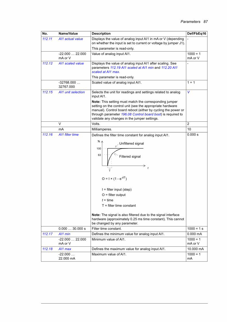
Parameters 87
112.11 AI1 actual value Displays the value of analog input AI1 in mA or V (depending on whether the input is set to current or voltage by jumper J1).
This parameter is read-only.
-
-22.000 … 22.000 mA or V
Value of analog input AI1. 1000 = 1 mA or V
112.12 AI1 scaled value Displays the value of analog input AI1 after scaling. See parameters 112.19 AI1 scaled at AI1 min and 112.20 AI1 scaled at AI1 max.
This parameter is read-only.
-
-32768.000 … 32767.000
Scaled value of analog input AI1. 1 = 1
112.15 AI1 unit selection Selects the unit for readings and settings related to analog input AI1.
Note: This setting must match the corresponding jumper setting on the control unit (see the appropriate hardware manual). Control board reboot (either by cycling the power or through parameter 196.08 Control board boot) is required to validate any changes in the jumper settings.
V
V Volts. 2
mA Milliamperes. 10
112.16 AI1 filter time Defines the filter time constant for analog input AI1.
Note: The signal is also filtered due to the signal interface hardware (approximately 0.25 ms time constant). This cannot be changed by any parameter.
0.000 s
0.000 … 30.000 s Filter time constant. 1000 = 1 s
112.17 AI1 min Defines the minimum value for analog input AI1. 0.000 mA
-22.000 … 22.000 mA or V
Minimum value of AI1. 1000 = 1 mA or V
112.18 AI1 max Defines the maximum value for analog input AI1. 10.000 mA
-22.000 … 22.000 mA
Maximum value of AI1. 1000 = 1 mA
No. Name/Value Description Def/FbEq16
63
%
100
Tt
O = I × (1 - e-t/T)
I = filter input (step)
O = filter output
t = time
T = filter time constant
Unfiltered signal
Filtered signal
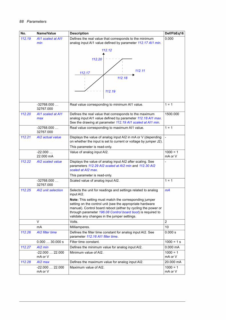
88 Parameters
112.19 AI1 scaled at AI1 min
Defines the real value that corresponds to the minimum analog input AI1 value defined by parameter 112.17 AI1 min.
0.000
-32768.000 … 32767.000
Real value corresponding to minimum AI1 value. 1 = 1
112.20 AI1 scaled at AI1 max
Defines the real value that corresponds to the maximum analog input AI1 value defined by parameter 112.18 AI1 max. See the drawing at parameter 112.19 AI1 scaled at AI1 min.
1500.000
-32768.000 … 32767.000
Real value corresponding to maximum AI1 value. 1 = 1
112.21 AI2 actual value Displays the value of analog input AI2 in mA or V (depending on whether the input is set to current or voltage by jumper J2).
This parameter is read-only.
-
-22.000 … 22.000 mA
Value of analog input AI2. 1000 = 1 mA or V
112.22 AI2 scaled value Displays the value of analog input AI2 after scaling. See parameters 112.29 AI2 scaled at AI2 min and 112.30 AI2 scaled at AI2 max.
This parameter is read-only.
-
-32768.000 … 32767.000
Scaled value of analog input AI2. 1 = 1
112.25 AI2 unit selection Selects the unit for readings and settings related to analog input AI2.
Note: This setting must match the corresponding jumper setting on the control unit (see the appropriate hardware manual). Control board reboot (either by cycling the power or through parameter 196.08 Control board boot) is required to validate any changes in the jumper settings.
mA
V Volts. 2
mA Milliamperes. 10
112.26 AI2 filter time Defines the filter time constant for analog input AI2. See parameter 112.16 AI1 filter time.
0.000 s
0.000 … 30.000 s Filter time constant. 1000 = 1 s
112.27 AI2 min Defines the minimum value for analog input AI2. 0.000 mA
-22.000 … 22.000 mA or V
Minimum value of AI2. 1000 = 1 mA or V
112.28 AI2 max Defines the maximum value for analog input AI2. 20.000 mA
-22.000 … 22.000 mA or V
Maximum value of AI2. 1000 = 1 mA or V
No. Name/Value Description Def/FbEq16
112.20
112.18
112.17
112.19
112.11
112.12

Parameters 89
112.29 AI2 scaled at AI2 min
Defines the real value that corresponds to the minimum analog input AI2 value defined by parameter 112.27 AI2 min.
0.000
-32768.000 … 32767.000
Real value corresponding to minimum AI2 value. 1 = 1
112.30 AI2 scaled at AI2 max
Defines the real value that corresponds to the maximum analog input AI2 value defined by parameter 112.28 AI2 max. See the drawing at parameter 112.29 AI2 scaled at AI2 min.
1500.000
-32768.000 … 32767.000
Real value corresponding to maximum AI2 value. 1 = 1
113113 Standard AO Configuration of analog outputs.
113.11 AO1 actual value Displays the value of AO1 in mA.
This parameter is read-only.
-
0.000 … 22.000 mA Value of AO1. 1000 = 1 mA
113.12 AO1 source Selects a signal to be connected to analog output AO1. Zero
Zero None. 0
DC voltage 101.01 DC voltage 1
Line current 101.02 Line current 2
AO1 data storage 113.91 AO1 data storage (page 91). 37
AO2 data storage 113.92 AO2 data storage (page 91). 38
Other The value is taken from another parameter. -
113.16 AO1 filter time Defines the filtering time constant for analog output AO1. 0.100 s
0.000 … 30.000 s Filter time constant. 1000 = 1 s
No. Name/Value Description Def/FbEq16
112.30
112.28
112.27
112.29
112.21
112.22
63
%
100
Tt
O = I × (1 - e-t/T)
I = filter input (step)
O = filter output
t = time
T = filter time constant
Unfiltered signal
Filtered signal

90 Parameters
113.17 AO1 source min Defines the real value of the signal (selected by parameter 113.12 AO1 source) that corresponds to the minimum AO1 output value (defined by parameter 113.19 AO1 out at AO1 src min).
0.0
-32768.0 … 32767.0
Real signal value corresponding to minimum AO1 output value.
1 = 1
113.18 AO1 source max Defines the real value of the signal (selected by parameter 113.12 AO1 source) that corresponds to the maximum AO1 output value (defined by parameter 113.20 AO1 out at AO1 src max). See parameter 113.17 AO1 source min.
100.0
-32768.0 … 32767.0
Real signal value corresponding to maximum AO1 output value.
1 = 1
113.19 AO1 out at AO1 src min
Defines the minimum output value for analog output AO1.
See also drawing at parameter 113.17 AO1 source min.
4.000 mA
0.000 … 22.000 mA Minimum AO1 output value. 1000 = 1 mA
113.20 AO1 out at AO1 src max
Defines the maximum output value for analog output AO1.
See also drawing at parameter 113.17 AO1 source min.
20.000 mA
0.000 … 22.000 mA Maximum AO1 output value. 1000 = 1 mA
113.21 AO2 actual value Displays the value of AO2 in mA.
This parameter is read-only.
-
0.000 … 22.000 mA Value of AO2. 1000 = 1 mA
113.22 AO2 source Selects a signal to be connected to analog output AO2.
For the selections, see parameter 113.12 AO1 source.
Zero
113.26 AO2 filter time Defines the filtering time constant for analog output AO2. See parameter 113.16 AO1 filter time.
0.100 s
0.000 … 30.000 s Filter time constant. 1000 = 1 s
No. Name/Value Description Def/FbEq16
IAO1 (mA)
113.20
113.19
113.18 113.17
113.18113.17
113.20
113.19
Signal (real)
selected by par. 113.12
IAO1 (mA)
Signal (real)
selected by par. 113.12

Parameters 91
113.27 AO2 source min Defines the real value of the signal (selected by parameter 113.22 AO2 source) that corresponds to the minimum AO2 output value (defined by parameter 113.29 AO2 out at AO2 src min).
0.0
-32768.0 … 32767.0
Real signal value corresponding to minimum AO2 output value.
1 = 1
113.28 AO2 source max Defines the real value of the signal (selected by parameter 113.22 AO2 source) that corresponds to the maximum AO2 output value (defined by parameter 113.30 AO2 out at AO2 src max). See parameter 113.27 AO2 source min.
100.0
-32768.0 … 32767.0
Real signal value corresponding to maximum AO2 output value.
1 = 1
113.29 AO2 out at AO2 src min
Defines the minimum output value for analog output AO2.
See also drawing at parameter 113.27 AO2 source min.
4.000 mA
0.000 … 22.000 mA Minimum AO2 output value. 1000 = 1 mA
113.30 AO2 out at AO2 src max
Defines the maximum output value for analog output AO2.
See also drawing at parameter 113.27 AO2 source min.
20.000 mA
0.000 … 22.000 mA Maximum AO2 output value. 1000 = 1 mA
113.91 AO1 data storage Storage parameter for controlling analog output AO1 eg. through fieldbus.In 113.12 AO1 source, select AO1 data storage. Then set this parameter as the target of the incoming value data.
0.00
-327.68 … 327.67 Storage parameter for AO1. 100 = 1
113.92 AO2 data storage Storage parameter for controlling analog output AO2 eg. through fieldbus.In 113.22 AO2 source, select AO2 data storage. Then set this parameter as the target of the incoming value data.
0.00
-327.68 … 327.67 Storage parameter for AO2. 100 = 1
No. Name/Value Description Def/FbEq16
IAO2 (mA)
113.30
113.29
113.28 113.27
113.28113.27
113.30
113.29
Signal (real)
selected by par. 113.22
IAO2 (mA)
Signal (real)
selected by par. 113.22
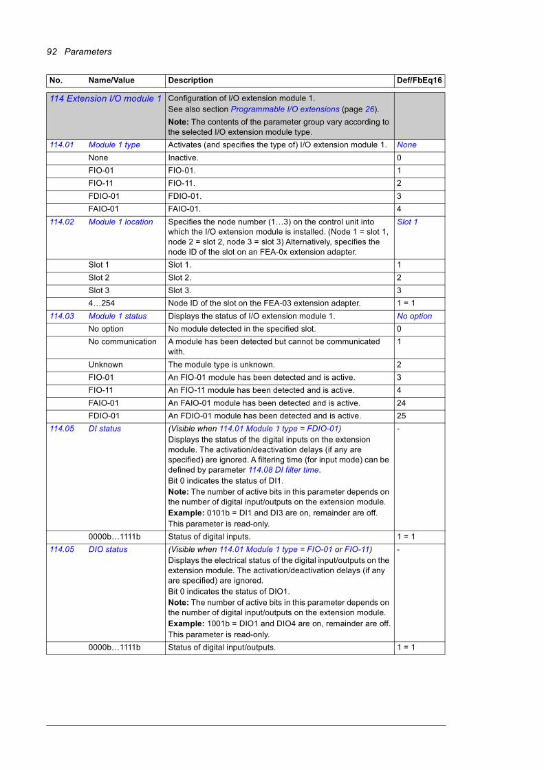
92 Parameters
114114 Extension I/O module 1 Configuration of I/O extension module 1.
See also section Programmable I/O extensions (page 26).
Note: The contents of the parameter group vary according to the selected I/O extension module type.
114.01 Module 1 type Activates (and specifies the type of) I/O extension module 1. None
None Inactive. 0
FIO-01 FIO-01. 1
FIO-11 FIO-11. 2
FDIO-01 FDIO-01. 3
FAIO-01 FAIO-01. 4
114.02 Module 1 location Specifies the node number (1…3) on the control unit into which the I/O extension module is installed. (Node 1 = slot 1, node 2 = slot 2, node 3 = slot 3) Alternatively, specifies the node ID of the slot on an FEA-0x extension adapter.
Slot 1
Slot 1 Slot 1. 1
Slot 2 Slot 2. 2
Slot 3 Slot 3. 3
4…254 Node ID of the slot on the FEA-03 extension adapter. 1 = 1
114.03 Module 1 status Displays the status of I/O extension module 1. No option
No option No module detected in the specified slot. 0
No communication A module has been detected but cannot be communicated with.
1
Unknown The module type is unknown. 2
FIO-01 An FIO-01 module has been detected and is active. 3
FIO-11 An FIO-11 module has been detected and is active. 4
FAIO-01 An FAIO-01 module has been detected and is active. 24
FDIO-01 An FDIO-01 module has been detected and is active. 25
114.05 DI status (Visible when 114.01 Module 1 type = FDIO-01)Displays the status of the digital inputs on the extension module. The activation/deactivation delays (if any are specified) are ignored. A filtering time (for input mode) can be defined by parameter 114.08 DI filter time.Bit 0 indicates the status of DI1.Note: The number of active bits in this parameter depends on the number of digital input/outputs on the extension module.Example: 0101b = DI1 and DI3 are on, remainder are off.This parameter is read-only.
-
0000b…1111b Status of digital inputs. 1 = 1
114.05 DIO status (Visible when 114.01 Module 1 type = FIO-01 or FIO-11)Displays the electrical status of the digital input/outputs on the extension module. The activation/deactivation delays (if any are specified) are ignored.Bit 0 indicates the status of DIO1.Note: The number of active bits in this parameter depends on the number of digital input/outputs on the extension module.Example: 1001b = DIO1 and DIO4 are on, remainder are off.This parameter is read-only.
-
0000b…1111b Status of digital input/outputs. 1 = 1
No. Name/Value Description Def/FbEq16
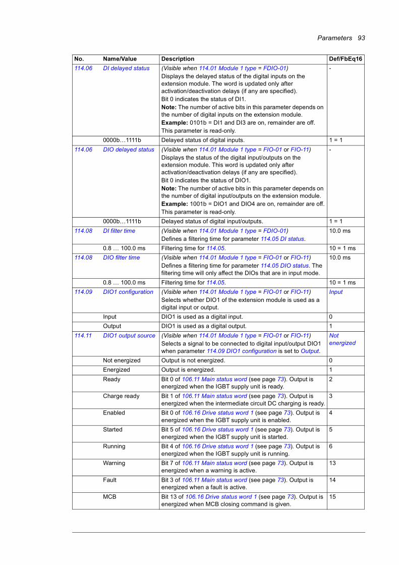
Parameters 93
114.06 DI delayed status (Visible when 114.01 Module 1 type = FDIO-01)Displays the delayed status of the digital inputs on the extension module. The word is updated only after activation/deactivation delays (if any are specified).Bit 0 indicates the status of DI1.Note: The number of active bits in this parameter depends on the number of digital inputs on the extension module.Example: 0101b = DI1 and DI3 are on, remainder are off.This parameter is read-only.
-
0000b…1111b Delayed status of digital inputs. 1 = 1
114.06 DIO delayed status (Visible when 114.01 Module 1 type = FIO-01 or FIO-11)Displays the status of the digital input/outputs on the extension module. This word is updated only after activation/deactivation delays (if any are specified).Bit 0 indicates the status of DIO1.Note: The number of active bits in this parameter depends on the number of digital input/outputs on the extension module.Example: 1001b = DIO1 and DIO4 are on, remainder are off.This parameter is read-only.
-
0000b…1111b Delayed status of digital input/outputs. 1 = 1
114.08 DI filter time (Visible when 114.01 Module 1 type = FDIO-01)Defines a filtering time for parameter 114.05 DI status.
10.0 ms
0.8 … 100.0 ms Filtering time for 114.05. 10 = 1 ms
114.08 DIO filter time (Visible when 114.01 Module 1 type = FIO-01 or FIO-11)Defines a filtering time for parameter 114.05 DIO status. The filtering time will only affect the DIOs that are in input mode.
10.0 ms
0.8 … 100.0 ms Filtering time for 114.05. 10 = 1 ms
114.09 DIO1 configuration (Visible when 114.01 Module 1 type = FIO-01 or FIO-11)Selects whether DIO1 of the extension module is used as a digital input or output.
Input
Input DIO1 is used as a digital input. 0
Output DIO1 is used as a digital output. 1
114.11 DIO1 output source (Visible when 114.01 Module 1 type = FIO-01 or FIO-11)Selects a signal to be connected to digital input/output DIO1 when parameter 114.09 DIO1 configuration is set to Output.
Not energized
Not energized Output is not energized. 0
Energized Output is energized. 1
Ready Bit 0 of 106.11 Main status word (see page 73). Output is energized when the IGBT supply unit is ready.
2
Charge ready Bit 1 of 106.11 Main status word (see page 73). Output is energized when the intermediate circuit DC charging is ready.
3
Enabled Bit 0 of 106.16 Drive status word 1 (see page 73). Output is energized when the IGBT supply unit is enabled.
4
Started Bit 5 of 106.16 Drive status word 1 (see page 73). Output is energized when the IGBT supply unit is started.
5
Running Bit 4 of 106.16 Drive status word 1 (see page 73). Output is energized when the IGBT supply unit is running.
6
Warning Bit 7 of 106.11 Main status word (see page 73). Output is energized when a warning is active.
13
Fault Bit 3 of 106.11 Main status word (see page 73). Output is energized when a fault is active.
14
MCB Bit 13 of 106.16 Drive status word 1 (see page 73). Output is energized when MCB closing command is given.
15
No. Name/Value Description Def/FbEq16
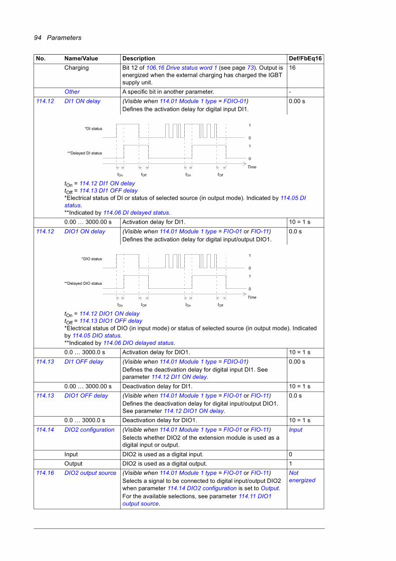
94 Parameters
Charging Bit 12 of 106.16 Drive status word 1 (see page 73). Output is energized when the external charging has charged the IGBT supply unit.
16
Other A specific bit in another parameter. -
114.12 DI1 ON delay (Visible when 114.01 Module 1 type = FDIO-01)Defines the activation delay for digital input DI1.
0.00 s
tOn = 114.12 DI1 ON delaytOff = 114.13 DI1 OFF delay*Electrical status of DI or status of selected source (in output mode). Indicated by 114.05 DI status.**Indicated by 114.06 DI delayed status.
0.00 … 3000.00 s Activation delay for DI1. 10 = 1 s
114.12 DIO1 ON delay (Visible when 114.01 Module 1 type = FIO-01 or FIO-11)Defines the activation delay for digital input/output DIO1.
0.0 s
tOn = 114.12 DIO1 ON delaytOff = 114.13 DIO1 OFF delay*Electrical status of DIO (in input mode) or status of selected source (in output mode). Indicated by 114.05 DIO status.**Indicated by 114.06 DIO delayed status.
0.0 … 3000.0 s Activation delay for DIO1. 10 = 1 s
114.13 DI1 OFF delay (Visible when 114.01 Module 1 type = FDIO-01)Defines the deactivation delay for digital input DI1. See parameter 114.12 DI1 ON delay.
0.00 s
0.00 … 3000.00 s Deactivation delay for DI1. 10 = 1 s
114.13 DIO1 OFF delay (Visible when 114.01 Module 1 type = FIO-01 or FIO-11)Defines the deactivation delay for digital input/output DIO1. See parameter 114.12 DIO1 ON delay.
0.0 s
0.0 … 3000.0 s Deactivation delay for DIO1. 10 = 1 s
114.14 DIO2 configuration (Visible when 114.01 Module 1 type = FIO-01 or FIO-11)Selects whether DIO2 of the extension module is used as a digital input or output.
Input
Input DIO2 is used as a digital input. 0
Output DIO2 is used as a digital output. 1
114.16 DIO2 output source (Visible when 114.01 Module 1 type = FIO-01 or FIO-11)Selects a signal to be connected to digital input/output DIO2 when parameter 114.14 DIO2 configuration is set to Output.For the available selections, see parameter 114.11 DIO1 output source.
Not energized
No. Name/Value Description Def/FbEq16
1
0
1
0
tOn tOff tOn tOff
*DI status
**Delayed DI status
Time
1
0
1
0
tOn tOff tOn tOff
*DIO status
**Delayed DIO status
Time
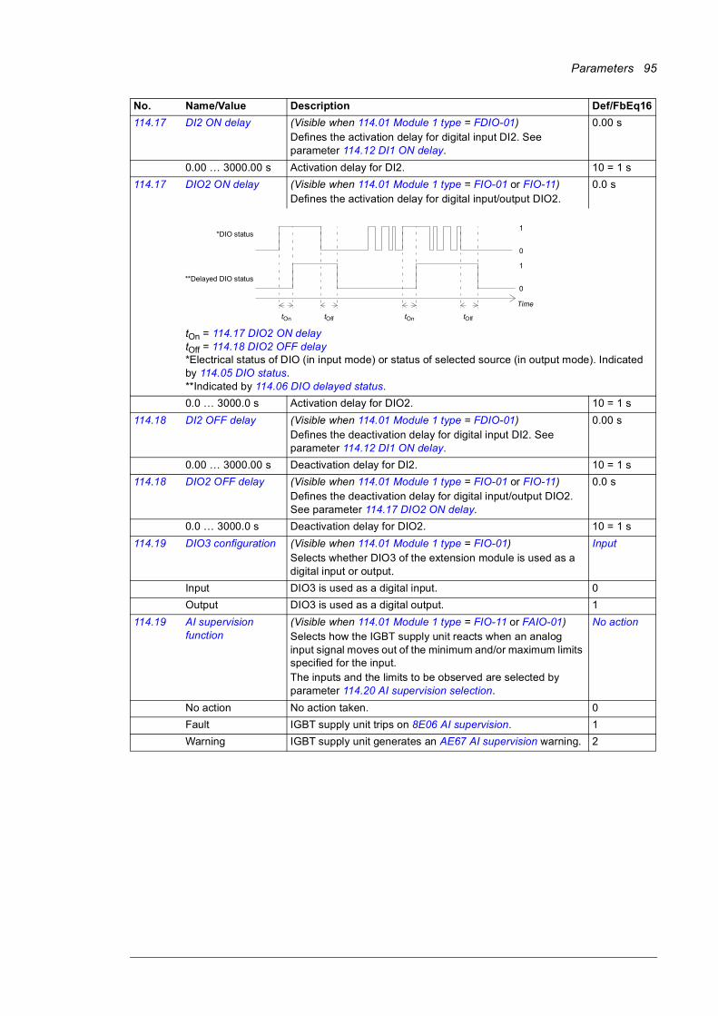
Parameters 95
114.17 DI2 ON delay (Visible when 114.01 Module 1 type = FDIO-01)Defines the activation delay for digital input DI2. See parameter 114.12 DI1 ON delay.
0.00 s
0.00 … 3000.00 s Activation delay for DI2. 10 = 1 s
114.17 DIO2 ON delay (Visible when 114.01 Module 1 type = FIO-01 or FIO-11)Defines the activation delay for digital input/output DIO2.
0.0 s
tOn = 114.17 DIO2 ON delaytOff = 114.18 DIO2 OFF delay*Electrical status of DIO (in input mode) or status of selected source (in output mode). Indicated by 114.05 DIO status.**Indicated by 114.06 DIO delayed status.
0.0 … 3000.0 s Activation delay for DIO2. 10 = 1 s
114.18 DI2 OFF delay (Visible when 114.01 Module 1 type = FDIO-01)Defines the deactivation delay for digital input DI2. See parameter 114.12 DI1 ON delay.
0.00 s
0.00 … 3000.00 s Deactivation delay for DI2. 10 = 1 s
114.18 DIO2 OFF delay (Visible when 114.01 Module 1 type = FIO-01 or FIO-11)Defines the deactivation delay for digital input/output DIO2. See parameter 114.17 DIO2 ON delay.
0.0 s
0.0 … 3000.0 s Deactivation delay for DIO2. 10 = 1 s
114.19 DIO3 configuration (Visible when 114.01 Module 1 type = FIO-01)Selects whether DIO3 of the extension module is used as a digital input or output.
Input
Input DIO3 is used as a digital input. 0
Output DIO3 is used as a digital output. 1
114.19 AI supervision function
(Visible when 114.01 Module 1 type = FIO-11 or FAIO-01)Selects how the IGBT supply unit reacts when an analog input signal moves out of the minimum and/or maximum limits specified for the input.The inputs and the limits to be observed are selected by parameter 114.20 AI supervision selection.
No action
No action No action taken. 0
Fault IGBT supply unit trips on 8E06 AI supervision. 1
Warning IGBT supply unit generates an AE67 AI supervision warning. 2
No. Name/Value Description Def/FbEq16
1
0
1
0
tOn tOff tOn tOff
*DIO status
**Delayed DIO status
Time

96 Parameters
114.20 AI supervision selection
(Visible when 114.01 Module 1 type = FIO-11 or FAIO-01)Specifies the analog input limits to be supervised. See parameter 114.19 AI supervision function.
0000h
0000h…FFFFh Activation of analog input supervision. 1 = 1
114.21 DIO3 output source (Visible when 114.01 Module 1 type = FIO-01)Selects a signal to be connected to digital input/output DIO3 when parameter 114.19 DIO3 configuration is set to Output.For the available selections, see parameter 114.11 DIO1 output source.
Not energized
114.22 DI3 ON delay (Visible when 114.01 Module 1 type = FDIO-01)Defines the activation delay for digital input DI3. See parameter 114.12 DI1 ON delay.
0.00 s
0.00 … 3000.00 s Activation delay for DI3. 10 = 1 s
114.22 DIO3 ON delay (Visible when 114.01 Module 1 type = FIO-01)Defines the activation delay for digital input/output DIO3.
0.0 s
tOn = 114.22 DIO3 ON delaytOff = 114.23 DIO3 OFF delay*Electrical status of DIO (in input mode) or status of selected source (in output mode). Indicated by 114.05 DIO status.**Indicated by 114.06 DIO delayed status.
0.0 … 3000.0 s Activation delay for DIO3. 10 = 1 s
114.22 AI force sel (Visible when 114.01 Module 1 type = FIO-11 or FAIO-01)The true readings of the analog inputs can be overridden for eg. testing purposes. A forced value parameter is provided for each analog input, and its value is applied whenever the corresponding bit in this parameter is 1.
00000000h
00000000h … FFFFFFFFh
Forced values selector for analog inputs. 1 = 1
No. Name/Value Description Def/FbEq16
Bit Name Description0 AI1 < MIN 1 = Minimum limit supervision of AI1 active.1 AI1 > MAX 1 = Maximum limit supervision of AI1 active.2 AI2 < MIN 1 = Minimum limit supervision of AI2 active.3 AI2 > MAX 1 = Maximum limit supervision of AI2 active.4 AI3 < MIN 1 = Minimum limit supervision of AI3 active.5 AI3 > MAX 1 = Maximum limit supervision of AI3 active.6…15 Reserved
1
0
1
0
tOn tOff tOn tOff
*DIO status
**Delayed DIO status
Time
Bit Value0 1 = Force AI1 to value of parameter 114.28 AI1 force data.1 1 = Force AI2 to value of parameter 114.43 AI2 force data.2 1 = Force AI3 to value of parameter 114.58 AI3 force data.3…31 Reserved.

Parameters 97
114.23 DI3 OFF delay (Visible when 114.01 Module 1 type = FDIO-01)Defines the deactivation delay for digital input DI3. See parameter 114.12 DI1 ON delay.
0.00 s
0.00 … 3000.00 s Deactivation delay for DI3. 10 = 1 s
114.23 DIO3 OFF delay (Visible when 114.01 Module 1 type = FIO-01)Defines the deactivation delay for digital input/output DIO3. See parameter 114.22 DIO3 ON delay.
0.0 s
0.0 … 3000.0 s Deactivation delay for DIO3. 10 = 1 s
114.24 DIO4 configuration (Visible when 114.01 Module 1 type = FIO-01)Selects whether DIO4 of the I/O extension module is used as a digital input or output.
Input
Input DIO4 is used as a digital input. 0
Output DIO4 is used as a digital output. 1
114.26 DIO4 output source (Visible when 114.01 Module 1 type = FIO-01)Selects a signal to be connected to digital input/output DIO4 when parameter 114.24 DIO4 configuration is set to Output.For the available selections, see parameter 114.11 DIO1 output source.
Not energized
114.26 AI1 actual value (Visible when 114.01 Module 1 type = FIO-11 or FAIO-01)Displays the value of analog input AI1 in mA or V (depending on whether the input is set to current or voltage).This parameter is read-only.
-
-22.000 … 22.000 mA or V
Value of analog input AI1. 1000 = 1 mA or V
114.27 DIO4 ON delay (Visible when 114.01 Module 1 type = FIO-01)Defines the activation delay for digital input/output DIO4.
0.0 s
tOn = 114.27 DIO4 ON delaytOff = 114.28 DIO4 OFF delay*Electrical status of DIO (in input mode) or status of selected source (in output mode). Indicated by 114.05 DIO status.**Indicated by 114.06 DIO delayed status.
0.0 … 3000.0 s Activation delay for DIO4. 10 = 1 s
114.27 AI1 scaled value (Visible when 114.01 Module 1 type = FIO-11 or FAIO-01)Displays the value of analog input AI1 after scaling. See parameter 114.35 AI1 scaled at AI1 min.This parameter is read-only.
-
-32768.000 … 32767.000
Scaled value of analog input AI1. 1 = 1
114.28 DIO4 OFF delay (Visible when 114.01 Module 1 type = FIO-01)Defines the deactivation delay for digital input/output DIO4. See parameter 114.27 DIO4 ON delay.
0.0 s
0.0 … 3000.0 s Deactivation delay for DIO4. 10 = 1 s
114.28 AI1 force data (Visible when 114.01 Module 1 type = FIO-11 or FAIO-01)Forced value that can be used instead of the true reading of the input. See parameter 114.22 AI force sel.
-
-22.000 … 22.000 mA or V
Forced value of analog input AI1. 1000 = 1 mA or V
No. Name/Value Description Def/FbEq16
1
0
1
0
tOn tOff tOn tOff
*DIO status
**Delayed DIO status
Time
98 Parameters
114.29 AI1 HW switch pos (Visible when 114.01 Module 1 type = FIO-11 or FAIO-01)Shows the position of the hardware current/voltage selector on the I/O extension module.Note: The setting of the current/voltage selector must match the unit selection made in parameter 114.30 AI1 unit selection.
-
V Volts. 2
mA Milliamperes. 10
114.30 AI1 unit selection (Visible when 114.01 Module 1 type = FIO-11 or FAIO-01)Selects the unit for readings and settings related to analog input AI1.Note: This setting must match the corresponding hardware setting on the I/O extension module (see the manual of the I/O extension module). The hardware setting is shown by parameter 114.29 AI1 HW switch pos.
mA
V Volts. 2
mA Milliamperes. 10
114.31 RO status (Visible when 114.01 Module 1 type = FIO-01 or FDIO-01)Status of relay outputs on the I/O extension module. Example: 00000001b = RO1 is energized, RO2 is de-energized.
-
0000h…FFFFh Status of relay outputs. 1 = 1
114.31 AI1 filter gain (Visible when 114.01 Module 1 type = FIO-11 or FAIO-01)Selects a hardware filtering time for AI1.See also parameter 114.32 AI1 filter time.
No filtering
No filtering No filtering. 0
125 us 125 microseconds. 1
250 us 250 microseconds. 2
500 us 500 microseconds. 3
1 ms 1 millisecond. 4
2 ms 2 milliseconds. 5
4 ms 4 milliseconds. 6
7.9375 ms 7.9375 milliseconds. 7
114.32 AI1 filter time (Visible when 114.01 Module 1 type = FIO-11 or FAIO-01)Defines the filter time constant for analog input AI1.
Note: The signal is also filtered due to the signal interface hardware. See parameter 114.31 AI1 filter gain.
0.040 s
0.000 … 30.000 s Filter time constant. 1000 = 1 s
No. Name/Value Description Def/FbEq16
63
%
100
Tt
O = I × (1 - e-t/T)
I = filter input (step)O = filter outputt = timeT = filter time constant
Unfiltered signal
Filtered signal

Parameters 99
114.33 AI1 min (Visible when 114.01 Module 1 type = FIO-11 or FAIO-01)Defines the minimum value for analog input AI1.
0.000 mA or V
-22.000 … 22.000 mA or V
Minimum value of AI1. 1000 = 1 mA or V
114.34 RO1 source (Visible when 114.01 Module 1 type = FIO-01 or FDIO-01)Selects a signal to be connected to relay output RO1.For the available selections, see parameter 114.11 DIO1 output source.
Not energized
114.34 AI1 max (Visible when 114.01 Module 1 type = FIO-11 or FAIO-01)Defines the maximum value for analog input AI1.
10.000 mA or V
-22.000 … 22.000 mA or V
Maximum value of AI1. 1000 = 1 mA or V
114.35 RO1 ON delay (Visible when 114.01 Module 1 type = FIO-01 or FDIO-01)Defines the activation delay for relay output RO1.
0.0 s
tOn = 114.35 RO1 ON delaytOff = 114.36 RO1 OFF delay
0.0 … 3000.0 s Activation delay for RO1. 10 = 1 s
114.35 AI1 scaled at AI1 min
(Visible when 114.01 Module 1 type = FIO-11 or FAIO-01)Defines the real value that corresponds to the minimum analog input AI1 value defined by parameter 114.33 AI1 min.
0.000
-32768.000 … 32767.000
Real value corresponding to minimum AI1 value. 1 = 1
114.36 RO1 OFF delay (Visible when 114.01 Module 1 type = FIO-01 or FDIO-01)Defines the deactivation delay for relay output RO1. See parameter 114.35 RO1 ON delay.
0.0 s
0.0 … 3000.0 s Deactivation delay for RO1. 10 = 1 s
114.36 AI1 scaled at AI1 max
(Visible when 114.01 Module 1 type = FIO-11 or FAIO-01)Defines the real value that corresponds to the maximum analog input AI1 value defined by parameter 114.34 AI1 max. See the drawing at parameter 114.35 AI1 scaled at AI1 min.
1500.0
-32768.000 … 32767.000
Real value corresponding to maximum AI1 value. 1 = 1
No. Name/Value Description Def/FbEq16
1
0
1
0
tOn tOff tOn tOff
Status of selectedsource
RO status
Time
114.36
114.34
114.33
114.35
AIin (114.26)
AIscaled (114.27)

100 Parameters
114.37 RO2 source (Visible when 114.01 Module 1 type = FIO-01 or FDIO-01)Selects a signal to be connected to relay output RO2.For the available selections, see parameter 114.11 DIO1 output source.
Not energized
114.38 RO2 ON delay (Visible when 114.01 Module 1 type = FIO-01 or FDIO-01)Defines the activation delay for relay output RO2.
0.0 s
tOn = 114.38 RO2 ON delaytOff = 114.39 RO2 OFF delay
0.0 … 3000.0 s Activation delay for RO2. 10 = 1 s
114.39 RO2 OFF delay (Visible when 114.01 Module 1 type = FIO-01 or FDIO-01)Defines the deactivation delay for relay output RO1. See parameter 114.35 RO1 ON delay.
0.0 s
0.0 … 3000.0 s Deactivation delay for RO2. 10 = 1 s
114.41 AI2 actual value (Visible when 114.01 Module 1 type = FIO-11 or FAIO-01)Displays the value of analog input AI2 in mA or V (depending on whether the input is set to current or voltage).This parameter is read-only.
-
-22.000 … 22.000 mA or V
Value of analog input AI2. 1000 = 1 mA or V
114.42 AI2 scaled value (Visible when 114.01 Module 1 type = FIO-11 or FAIO-01)Displays the value of analog input AI2 after scaling. See parameter 114.50 AI2 scaled at AI2 min.This parameter is read-only.
-
-32768.000 … 32767.000
Scaled value of analog input AI2. 1 = 1
114.43 AI2 force data (Visible when 114.01 Module 1 type = FIO-11 or FAIO-01)Forced value that can be used instead of the true reading of the input. See parameter 114.22 AI force sel.
0.000 mA
-22.000 … 22.000 mA or V
Forced value of analog input AI2. 1000 = 1 mA or V
114.44 AI2 HW switch pos (Visible when 114.01 Module 1 type = FIO-11 or FAIO-01)Shows the position of the hardware current/voltage selector on the I/O extension module.Note: The setting of the current/voltage selector must match the unit selection made in parameter 114.45 AI2 unit selection.
-
V Volts. 2
mA Milliamperes. 10
114.45 AI2 unit selection (Visible when 114.01 Module 1 type = FIO-11 or FAIO-01)Selects the unit for readings and settings related to analog input AI2.Note: This setting must match the corresponding hardware setting on the I/O extension module (see the manual of the I/O extension module). The hardware setting is shown by parameter 114.44 AI2 HW switch pos.
mA
V Volts. 2
mA Milliamperes. 10
No. Name/Value Description Def/FbEq16
1
0
1
0
tOn tOff tOn tOff
Status of selectedsource
RO status
Time
Parameters 101
114.46 AI2 filter gain (Visible when 114.01 Module 1 type = FIO-11 or FAIO-01)Selects a hardware filtering time for AI2.See also parameter 114.47 AI2 filter time.
No filtering
No filtering No filtering. 0
125 us 125 microseconds. 1
250 us 250 microseconds. 2
500 us 500 microseconds. 3
1 ms 1 millisecond. 4
2 ms 2 milliseconds. 5
4 ms 4 milliseconds. 6
7.9375 ms 7.9375 milliseconds. 7
114.47 AI2 filter time (Visible when 114.01 Module 1 type = FIO-11 or FAIO-01)Defines the filter time constant for analog input AI2.
Note: The signal is also filtered due to the signal interface hardware. See parameter 114.46 AI2 filter gain.
0.100 s
0.000 … 30.000 s Filter time constant. 1000 = 1 s
114.48 AI2 min (Visible when 114.01 Module 1 type = FIO-11 or FAIO-01)Defines the minimum value for analog input AI2.
0.000 mA or V
-22.000 … 22.000 mA or V
Minimum value of AI2. 1000 = 1 mA or V
114.49 AI2 max (Visible when 114.01 Module 1 type = FIO-11 or FAIO-01)Defines the maximum value for analog input AI2.
10.000 mA or V
-22.000 … 22.000 mA or V
Maximum value of AI2. 1000 = 1 mA or V
No. Name/Value Description Def/FbEq16
63
%
100
Tt
O = I × (1 - e-t/T)
I = filter input (step)O = filter outputt = timeT = filter time constant
Unfiltered signal
Filtered signal
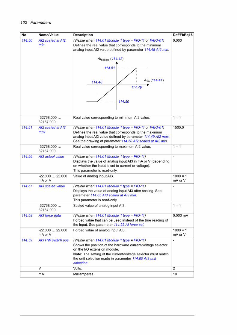
102 Parameters
114.50 AI2 scaled at AI2 min
(Visible when 114.01 Module 1 type = FIO-11 or FAIO-01)Defines the real value that corresponds to the minimum analog input AI2 value defined by parameter 114.48 AI2 min.
0.000
-32768.000 … 32767.000
Real value corresponding to minimum AI2 value. 1 = 1
114.51 AI2 scaled at AI2 max
(Visible when 114.01 Module 1 type = FIO-11 or FAIO-01)Defines the real value that corresponds to the maximum analog input AI2 value defined by parameter 114.49 AI2 max. See the drawing at parameter 114.50 AI2 scaled at AI2 min.
1500.0
-32768.000 … 32767.000
Real value corresponding to maximum AI2 value. 1 = 1
114.56 AI3 actual value (Visible when 114.01 Module 1 type = FIO-11)Displays the value of analog input AI3 in mA or V (depending on whether the input is set to current or voltage).This parameter is read-only.
-
-22.000 … 22.000 mA or V
Value of analog input AI3. 1000 = 1 mA or V
114.57 AI3 scaled value (Visible when 114.01 Module 1 type = FIO-11)Displays the value of analog input AI3 after scaling. See parameter 114.65 AI3 scaled at AI3 min.This parameter is read-only.
-
-32768.000 … 32767.000
Scaled value of analog input AI3. 1 = 1
114.58 AI3 force data (Visible when 114.01 Module 1 type = FIO-11)Forced value that can be used instead of the true reading of the input. See parameter 114.22 AI force sel.
0.000 mA
-22.000 … 22.000 mA or V
Forced value of analog input AI3. 1000 = 1 mA or V
114.59 AI3 HW switch pos (Visible when 114.01 Module 1 type = FIO-11)Shows the position of the hardware current/voltage selector on the I/O extension module.Note: The setting of the current/voltage selector must match the unit selection made in parameter 114.60 AI3 unit selection.
-
V Volts. 2
mA Milliamperes. 10
No. Name/Value Description Def/FbEq16
114.51
114.49
114.48
114.50
AIin (114.41)
AIscaled (114.42)

Parameters 103
114.60 AI3 unit selection (Visible when 114.01 Module 1 type = FIO-11)Selects the unit for readings and settings related to analog input AI3.Note: This setting must match the corresponding hardware setting on the I/O extension module (see the manual of the I/O extension module). The hardware setting is shown by parameter 114.59 AI3 HW switch pos.
mA
V Volts. 2
mA Milliamperes. 10
114.61 AI3 filter gain (Visible when 114.01 Module 1 type = FIO-11)Selects a hardware filtering time for AI3.See also parameter 114.62 AI3 filter time.
No filtering
No filtering No filtering. 0
125 us 125 microseconds. 1
250 us 250 microseconds. 2
500 us 500 microseconds. 3
1 ms 1 millisecond. 4
2 ms 2 milliseconds. 5
4 ms 4 milliseconds. 6
7.9375 ms 7.9375 milliseconds. 7
114.62 AI3 filter time (Visible when 114.01 Module 1 type = FIO-11)Defines the filter time constant for analog input AI3.
Note: The signal is also filtered due to the signal interface hardware. See parameter 114.61 AI3 filter gain.
0.100 s
0.000 … 30.000 s Filter time constant. 1000 = 1 s
114.63 AI3 min (Visible when 114.01 Module 1 type = FIO-11)Defines the minimum value for analog input AI3.
0.000 mA or V
-22.000 … 22.000 mA or V
Minimum value of AI3. 1000 = 1 mA or V
114.64 AI3 max (Visible when 114.01 Module 1 type = FIO-11)Defines the maximum value for analog input AI3.
10.000 mA or V
-22.000 … 22.000 mA or V
Maximum value of AI3. 1000 = 1 mA or V
No. Name/Value Description Def/FbEq16
63
%
100
Tt
O = I × (1 - e-t/T)
I = filter input (step)O = filter outputt = timeT = filter time constant
Unfiltered signal
Filtered signal

104 Parameters
114.65 AI3 scaled at AI3 min
(Visible when 114.01 Module 1 type = FIO-11)Defines the real value that corresponds to the minimum analog input AI3 value defined by parameter 114.63 AI3 min.
0.000
-32768.000 … 32767.000
Real value corresponding to minimum AI3 value. 1 = 1
114.66 AI3 scaled at AI3 max
(Visible when 114.01 Module 1 type = FIO-11)Defines the real value that corresponds to the maximum analog input AI3 value defined by parameter 114.64 AI3 max. See the drawing at parameter 114.65 AI3 scaled at AI3 min.
1500.0
-32768.000 … 32767.000
Real value corresponding to maximum AI3 value. 1 = 1
114.71 AO force selection (Visible when 114.01 Module 1 type = FIO-11 or FAIO-01)The value of the analog output can be overridden for eg. testing purposes. A forced value parameter (114.78 AO1 force data) is provided for the analog output, and its value is applied whenever the corresponding bit in this parameter is 1.
00000000h
00000000h … FFFFFFFFh
Forced values selector for analog outputs. 1 = 1
114.76 AO1 actual value (Visible when 114.01 Module 1 type = FIO-11 or FAIO-01)Displays the value of AO1 in mA.This parameter is read-only.
-
0.000 … 22.000 mA Value of AO1. 1000 = 1 mA
114.77 AO1 source (Visible when 114.01 Module 1 type = FIO-11 or FAIO-01)Selects a signal to be connected to analog output AO1. Alternatively, sets the output to excitation mode to feed a constant current to a temperature sensor.
Zero
Zero None. 0
DC voltage 101.01 DC voltage 1
Line current 101.02 Line current 2
Other The value is taken from another parameter. -
114.78 AO1 force data (Visible when 114.01 Module 1 type = FIO-11 or FAIO-01)Forced value that can be used instead of the selected output signal. See parameter 114.71 AO force selection.
0.000 mA
0.000 … 22.000 mA Forced value of analog output AI1. 1000 = 1 mA
No. Name/Value Description Def/FbEq16
114.66
114.64
114.63
114.65
AIin (114.56)
AIscaled (114.57)
Bit Value0 1 = Force AO1 to value of parameter 114.78 AO1 force data.1…31 Reserved.
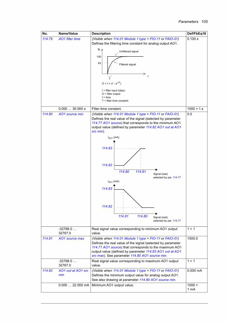
Parameters 105
114.79 AO1 filter time (Visible when 114.01 Module 1 type = FIO-11 or FAIO-01)Defines the filtering time constant for analog output AO1.
0.100 s
0.000 … 30.000 s Filter time constant. 1000 = 1 s
114.80 AO1 source min (Visible when 114.01 Module 1 type = FIO-11 or FAIO-01)Defines the real value of the signal (selected by parameter 114.77 AO1 source) that corresponds to the minimum AO1 output value (defined by parameter 114.82 AO1 out at AO1 src min).
0.0
-32768.0 … 32767.0
Real signal value corresponding to minimum AO1 output value.
1 = 1
114.81 AO1 source max (Visible when 114.01 Module 1 type = FIO-11 or FAIO-01)Defines the real value of the signal (selected by parameter 114.77 AO1 source) that corresponds to the maximum AO1 output value (defined by parameter 114.83 AO1 out at AO1 src max). See parameter 114.80 AO1 source min.
1500.0
-32768.0 … 32767.0
Real signal value corresponding to maximum AO1 output value.
1 = 1
114.82 AO1 out at AO1 src min
(Visible when 114.01 Module 1 type = FIO-11 or FAIO-01)Defines the minimum output value for analog output AO1.See also drawing at parameter 114.80 AO1 source min.
0.000 mA
0.000 … 22.000 mA Minimum AO1 output value. 1000 = 1 mA
No. Name/Value Description Def/FbEq16
63
%
100
Tt
O = I × (1 - e-t/T)
I = filter input (step)O = filter outputt = timeT = filter time constant
Unfiltered signal
Filtered signal
IAO1 (mA)
114.83
114.82
114.81 114.80
114.81114.80
114.83
114.82
Signal (real)selected by par. 114.77
IAO1 (mA)
Signal (real)selected by par. 114.77
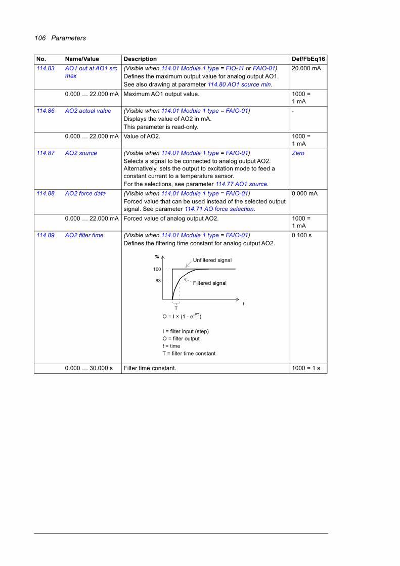
106 Parameters
114.83 AO1 out at AO1 src max
(Visible when 114.01 Module 1 type = FIO-11 or FAIO-01)Defines the maximum output value for analog output AO1.See also drawing at parameter 114.80 AO1 source min.
20.000 mA
0.000 … 22.000 mA Maximum AO1 output value. 1000 = 1 mA
114.86 AO2 actual value (Visible when 114.01 Module 1 type = FAIO-01)Displays the value of AO2 in mA.This parameter is read-only.
-
0.000 … 22.000 mA Value of AO2. 1000 = 1 mA
114.87 AO2 source (Visible when 114.01 Module 1 type = FAIO-01)Selects a signal to be connected to analog output AO2. Alternatively, sets the output to excitation mode to feed a constant current to a temperature sensor.For the selections, see parameter 114.77 AO1 source.
Zero
114.88 AO2 force data (Visible when 114.01 Module 1 type = FAIO-01)Forced value that can be used instead of the selected output signal. See parameter 114.71 AO force selection.
0.000 mA
0.000 … 22.000 mA Forced value of analog output AO2. 1000 = 1 mA
114.89 AO2 filter time (Visible when 114.01 Module 1 type = FAIO-01)Defines the filtering time constant for analog output AO2.
0.100 s
0.000 … 30.000 s Filter time constant. 1000 = 1 s
No. Name/Value Description Def/FbEq16
63
%
100
Tt
O = I × (1 - e-t/T)
I = filter input (step)O = filter outputt = timeT = filter time constant
Unfiltered signal
Filtered signal

Parameters 107
114.90 AO2 source min (Visible when 114.01 Module 1 type = FAIO-01)Defines the real value of the signal (selected by parameter 114.87 AO2 source) that corresponds to the minimum AO2 output value (defined by parameter 114.92 AO2 out at AO2 src min).
0.0
-32768.0 … 32767.0
Real signal value corresponding to minimum AO2 output value.
1 = 1
114.91 AO2 source max (Visible when 114.01 Module 1 type = FAIO-01)Defines the real value of the signal (selected by parameter 114.87 AO2 source) that corresponds to the maximum AO2 output value (defined by parameter 114.93 AO2 out at AO2 src max). See parameter 114.90 AO2 source min.
100.0
-32768.0 … 32767.0
Real signal value corresponding to maximum AO2 output value.
1 = 1
114.92 AO2 out at AO2 src min
(Visible when 114.01 Module 1 type = FAIO-01)Defines the minimum output value for analog output AO2.See also drawing at parameter 114.90 AO2 source min.
0.000 mA
0.000 … 22.000 mA Minimum AO2 output value. 1000 = 1 mA
114.93 AO2 out at AO2 src max
(Visible when 114.01 Module 1 type = FAIO-01)Defines the maximum output value for analog output AO2.See also drawing at parameter 114.90 AO2 source min.
10.000 mA
0.000 … 22.000 mA Maximum AO2 output value. 1000 = 1 mA
115115 Extension I/O module 2 Configuration of I/O extension module 2.
See also section Programmable I/O extensions (page 26).
Note: The contents of the parameter group vary according to the selected I/O extension module type.
115.01 Module 2 type See parameter 114.01 Module 1 type. None
115.02 Module 2 location See parameter 114.02 Module 1 location. 1 (Slot 1)
115.03 Module 2 status See parameter 114.03 Module 1 status. No option
115.05 DI status (Visible when 115.01 Module 2 type = FDIO-01)See parameter 114.05 DI status.
-
No. Name/Value Description Def/FbEq16
IAO2 (mA)
114.91114.90
114.93
114.92
IAO2 (mA)
Signal (real)selected by par. 114.87
114.93
114.92
114.91 114.90Signal (real)selected by par. 114.87

108 Parameters
115.05 DIO status (Visible when 115.01 Module 2 type = FIO-01 or FIO-11)See parameter 114.05 DIO status.
-
115.06 DI delayed status (Visible when 115.01 Module 2 type = FDIO-01)See parameter 114.06 DI delayed status.
-
115.06 DIO delayed status (Visible when 115.01 Module 2 type = FIO-01 or FIO-11)See parameter 114.06 DIO delayed status.
-
115.08 DI filter time (Visible when 115.01 Module 2 type = FDIO-01)See parameter 114.08 DI filter time.
10.0 ms
115.08 DIO filter time (Visible when 115.01 Module 2 type = FIO-01 or FIO-11)See parameter 114.08 DIO filter time.
10.0 ms
115.09 DIO1 configuration (Visible when 115.01 Module 2 type = FIO-01 or FIO-11)See parameter 114.09 DIO1 configuration.
Input
115.11 DIO1 output source (Visible when 115.01 Module 2 type = FIO-01 or FIO-11)See parameter 114.11 DIO1 output source.
Not energized
115.12 DI1 ON delay (Visible when 115.01 Module 2 type = FDIO-01)See parameter 114.12 DI1 ON delay.
0.00 s
115.12 DIO1 ON delay (Visible when 115.01 Module 2 type = FIO-01 or FIO-11)See parameter 114.12 DIO1 ON delay.
0.0 s
115.13 DI1 OFF delay (Visible when 115.01 Module 2 type = FDIO-01)See parameter 114.13 DI1 OFF delay.
0.00 s
115.13 DIO1 OFF delay (Visible when 115.01 Module 2 type = FIO-01 or FIO-11)See parameter 114.13 DIO1 OFF delay.
0.0 s
115.14 DIO2 configuration (Visible when 115.01 Module 2 type = FIO-01 or FIO-11)See parameter 114.14 DIO2 configuration.
Input
115.16 DIO2 output source (Visible when 115.01 Module 2 type = FIO-01 or FIO-11)See parameter 114.16 DIO2 output source.
Not energized
115.17 DI2 ON delay (Visible when 115.01 Module 2 type = FDIO-01)See parameter 114.17 DI2 ON delay.
0.00 s
115.17 DIO2 ON delay (Visible when 115.01 Module 2 type = FIO-01 or FIO-11)See parameter 114.17 DIO2 ON delay.
0.0 s
115.18 DI2 OFF delay (Visible when 115.01 Module 2 type = FDIO-01)See parameter 114.18 DI2 OFF delay.
0.00 s
115.18 DIO2 OFF delay (Visible when 115.01 Module 2 type = FIO-01 or FIO-11)See parameter 114.18 DIO2 OFF delay.
0.0 s
115.19 DIO3 configuration (Visible when 115.01 Module 2 type = FIO-01)See parameter 114.19 DIO3 configuration.
Input
115.19 AI supervision function
(Visible when 115.01 Module 2 type = FIO-11 or FAIO-01)See parameter 114.19 AI supervision function.
No action
115.20 AI supervision selection
(Visible when 115.01 Module 2 type = FIO-11 or FAIO-01)See parameter 114.20 AI supervision selection.
0000h
115.21 DIO3 output source (Visible when 115.01 Module 2 type = FIO-01)See parameter 114.21 DIO3 output source.
Not energized
115.22 DI3 ON delay (Visible when 115.01 Module 2 type = FDIO-01)See parameter 114.22 DI3 ON delay.
0.00 s
115.22 DIO3 ON delay (Visible when 115.01 Module 2 type = FIO-01)See parameter 114.22 DIO3 ON delay.
0.0 s
115.22 AI force sel (Visible when 115.01 Module 2 type = FIO-11 or FAIO-01)See parameter 114.22 AI force sel.
00000000h
115.23 DI3 OFF delay (Visible when 115.01 Module 2 type = FDIO-01)See parameter 114.23 DI3 OFF delay.
0.00 s
115.23 DIO3 OFF delay (Visible when 115.01 Module 2 type = FIO-01)See parameter 114.23 DIO3 OFF delay.
0.0 s
No. Name/Value Description Def/FbEq16

Parameters 109
115.24 DIO4 configuration (Visible when 115.01 Module 2 type = FIO-01)See parameter 114.24 DIO4 configuration.
Input
115.26 DIO4 output source (Visible when 115.01 Module 2 type = FIO-01)See parameter 114.26 DIO4 output source.
Not energized
115.26 AI1 actual value (Visible when 115.01 Module 2 type = FIO-11 or FAIO-01)See parameter 114.26 AI1 actual value.
-
115.27 DIO4 ON delay (Visible when 115.01 Module 2 type = FIO-01)See parameter 114.27 DIO4 ON delay.
0.0 s
115.27 AI1 scaled value (Visible when 115.01 Module 2 type = FIO-11 or FAIO-01)See parameter 114.27 AI1 scaled value.
-
115.28 DIO4 OFF delay (Visible when 115.01 Module 2 type = FIO-01)See parameter 114.28 DIO4 OFF delay.
0.0 s
115.28 AI1 force data (Visible when 115.01 Module 2 type = FIO-11 or FAIO-01)See parameter 114.28 AI1 force data.
-
115.29 AI1 HW switch pos (Visible when 115.01 Module 2 type = FIO-11 or FAIO-01)See parameter 114.29 AI1 HW switch pos.
-
115.30 AI1 unit selection (Visible when 115.01 Module 2 type = FIO-11 or FAIO-01)See parameter 114.30 AI1 unit selection.
mA
115.31 RO status (Visible when 115.01 Module 2 type = FIO-01 or FDIO-01)See parameter 114.31 RO status.
-
115.31 AI1 filter gain (Visible when 115.01 Module 2 type = FIO-11 or FAIO-01)See parameter 114.31 AI1 filter gain.
No filtering
115.32 AI1 filter time (Visible when 115.01 Module 2 type = FIO-11 or FAIO-01)See parameter 114.32 AI1 filter time.
0.040 s
115.33 AI1 min (Visible when 115.01 Module 2 type = FIO-11 or FAIO-01)See parameter 114.33 AI1 min.
0.000 mA or V
115.34 RO1 source (Visible when 115.01 Module 2 type = FIO-01 or FDIO-01)See parameter 114.34 RO1 source.
Not energized
115.34 AI1 max (Visible when 115.01 Module 2 type = FIO-11 or FAIO-01)See parameter 114.34 AI1 max.
10.000 mA or V
115.35 RO1 ON delay (Visible when 115.01 Module 2 type = FIO-01 or FDIO-01)See parameter 114.35 RO1 ON delay.
0.0 s
115.35 AI1 scaled at AI1 min
(Visible when 115.01 Module 2 type = FIO-11 or FAIO-01)See parameter 114.35 AI1 scaled at AI1 min.
0.000
115.36 RO1 OFF delay (Visible when 115.01 Module 2 type = FIO-01 or FDIO-01)See parameter 114.36 RO1 OFF delay.
0.0 s
115.36 AI1 scaled at AI1 max
(Visible when 115.01 Module 2 type = FIO-11 or FAIO-01)See parameter 114.36 AI1 scaled at AI1 max.
1500.0
115.37 RO2 source (Visible when 115.01 Module 2 type = FIO-01 or FDIO-01)See parameter 114.37 RO2 source.
Not energized
115.38 RO2 ON delay (Visible when 115.01 Module 2 type = FIO-01 or FDIO-01)See parameter 114.38 RO2 ON delay.
0.0 s
115.39 RO2 OFF delay (Visible when 115.01 Module 2 type = FIO-01 or FDIO-01)See parameter 114.39 RO2 OFF delay.
0.0 s
115.41 AI2 actual value (Visible when 115.01 Module 2 type = FIO-11 or FAIO-01)See parameter 114.41 AI2 actual value.
-
115.42 AI2 scaled value (Visible when 115.01 Module 2 type = FIO-11 or FAIO-01)See parameter 114.42 AI2 scaled value.
-
115.43 AI2 force data (Visible when 115.01 Module 2 type = FIO-11 or FAIO-01)See parameter 114.43 AI2 force data.
0.000 mA
115.44 AI2 HW switch pos (Visible when 115.01 Module 2 type = FIO-11 or FAIO-01)See parameter 114.44 AI2 HW switch pos.
-
No. Name/Value Description Def/FbEq16

110 Parameters
115.45 AI2 unit selection (Visible when 115.01 Module 2 type = FIO-11 or FAIO-01)See parameter 114.45 AI2 unit selection.
mA
115.46 AI2 filter gain (Visible when 115.01 Module 2 type = FIO-11 or FAIO-01)See parameter 114.46 AI2 filter gain.
No filtering
115.47 AI2 filter time (Visible when 115.01 Module 2 type = FIO-11 or FAIO-01)See parameter 114.47 AI2 filter time.
0.100 s
115.48 AI2 min (Visible when 115.01 Module 2 type = FIO-11 or FAIO-01)See parameter 114.48 AI2 min.
0.000 mA or V
115.49 AI2 max (Visible when 115.01 Module 2 type = FIO-11 or FAIO-01)See parameter 114.49 AI2 max.
10.000 mA or V
115.50 AI2 scaled at AI2 min
(Visible when 115.01 Module 2 type = FIO-11 or FAIO-01)See parameter 114.50 AI2 scaled at AI2 min.
0.000
115.51 AI2 scaled at AI2 max
(Visible when 115.01 Module 2 type = FIO-11 or FAIO-01)See parameter 114.51 AI2 scaled at AI2 max.
1500.0
115.56 AI3 actual value (Visible when 115.01 Module 2 type = FIO-11)See parameter 114.56 AI3 actual value.
-
115.57 AI3 scaled value (Visible when 115.01 Module 2 type = FIO-11)See parameter 114.57 AI3 scaled value.
-
115.58 AI3 force data (Visible when 115.01 Module 2 type = FIO-11)See parameter 114.58 AI3 force data.
0.000 mA
115.59 AI3 HW switch pos (Visible when 115.01 Module 2 type = FIO-11)See parameter 114.59 AI3 HW switch pos.
-
115.60 AI3 unit selection (Visible when 115.01 Module 2 type = FIO-11)See parameter 114.60 AI3 unit selection.
mA
115.61 AI3 filter gain (Visible when 115.01 Module 2 type = FIO-11)See parameter 114.61 AI3 filter gain.
No filtering
115.62 AI3 filter time (Visible when 115.01 Module 2 type = FIO-11)See parameter 114.62 AI3 filter time.
0.100 s
115.63 AI3 min (Visible when 115.01 Module 2 type = FIO-11)See parameter 114.63 AI3 min.
0.000 mA or V
115.64 AI3 max (Visible when 115.01 Module 2 type = FIO-11)See parameter 114.64 AI3 max.
10.000 mA or V
115.65 AI3 scaled at AI3 min
(Visible when 115.01 Module 2 type = FIO-11)See parameter 114.65 AI3 scaled at AI3 min.
0.000
115.66 AI3 scaled at AI3 max
(Visible when 115.01 Module 2 type = FIO-11)See parameter 114.66 AI3 scaled at AI3 max.
1500.0
115.71 AO force selection (Visible when 115.01 Module 2 type = FIO-11 or FAIO-01)See parameter 114.71 AO force selection.
00000000h
115.76 AO1 actual value (Visible when 115.01 Module 2 type = FIO-11 or FAIO-01)See parameter 114.76 AO1 actual value.
-
115.77 AO1 source (Visible when 115.01 Module 2 type = FIO-11 or FAIO-01)See parameter 114.77 AO1 source.
Zero
115.78 AO1 force data (Visible when 115.01 Module 2 type = FIO-11 or FAIO-01)See parameter 114.78 AO1 force data.
0.000 mA
115.79 AO1 filter time (Visible when 115.01 Module 2 type = FIO-11 or FAIO-01)See parameter 114.79 AO1 filter time.
0.100 s
115.80 AO1 source min (Visible when 115.01 Module 2 type = FIO-11 or FAIO-01)See parameter 114.80 AO1 source min.
0.0
115.81 AO1 source max (Visible when 115.01 Module 2 type = FIO-11 or FAIO-01)See parameter 114.81 AO1 source max.
1500.0
115.82 AO1 out at AO1 src min
(Visible when 115.01 Module 2 type = FIO-11 or FAIO-01)See parameter 114.82 AO1 out at AO1 src min.
0.000 mA
No. Name/Value Description Def/FbEq16
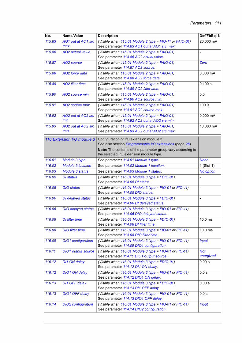
Parameters 111
115.83 AO1 out at AO1 src max
(Visible when 115.01 Module 2 type = FIO-11 or FAIO-01)See parameter 114.83 AO1 out at AO1 src max.
20.000 mA
115.86 AO2 actual value (Visible when 115.01 Module 2 type = FAIO-01)See parameter 114.86 AO2 actual value.
-
115.87 AO2 source (Visible when 115.01 Module 2 type = FAIO-01)See parameter 114.87 AO2 source.
Zero
115.88 AO2 force data (Visible when 115.01 Module 2 type = FAIO-01)See parameter 114.88 AO2 force data.
0.000 mA
115.89 AO2 filter time (Visible when 115.01 Module 2 type = FAIO-01)See parameter 114.89 AO2 filter time.
0.100 s
115.90 AO2 source min (Visible when 115.01 Module 2 type = FAIO-01)See parameter 114.90 AO2 source min.
0.0
115.91 AO2 source max (Visible when 115.01 Module 2 type = FAIO-01)See parameter 114.91 AO2 source max.
100.0
115.92 AO2 out at AO2 src min
(Visible when 115.01 Module 2 type = FAIO-01)See parameter 114.92 AO2 out at AO2 src min.
0.000 mA
115.93 AO2 out at AO2 src max
(Visible when 115.01 Module 2 type = FAIO-01)See parameter 114.93 AO2 out at AO2 src max.
10.000 mA
116116 Extension I/O module 3 Configuration of I/O extension module 3.
See also section Programmable I/O extensions (page 26).
Note: The contents of the parameter group vary according to the selected I/O extension module type.
116.01 Module 3 type See parameter 114.01 Module 1 type. None
116.02 Module 3 location See parameter 114.02 Module 1 location. 1 (Slot 1)
116.03 Module 3 status See parameter 114.03 Module 1 status. No option
116.05 DI status (Visible when 116.01 Module 3 type = FDIO-01)See parameter 114.05 DI status.
-
116.05 DIO status (Visible when 116.01 Module 3 type = FIO-01 or FIO-11)See parameter 114.05 DIO status.
-
116.06 DI delayed status (Visible when 116.01 Module 3 type = FDIO-01)See parameter 114.06 DI delayed status.
-
116.06 DIO delayed status (Visible when 116.01 Module 3 type = FIO-01 or FIO-11)See parameter 114.06 DIO delayed status.
-
116.08 DI filter time (Visible when 116.01 Module 3 type = FDIO-01)See parameter 114.08 DI filter time.
10.0 ms
116.08 DIO filter time (Visible when 116.01 Module 3 type = FIO-01 or FIO-11)See parameter 114.08 DIO filter time.
10.0 ms
116.09 DIO1 configuration (Visible when 116.01 Module 3 type = FIO-01 or FIO-11)See parameter 114.09 DIO1 configuration.
Input
116.11 DIO1 output source (Visible when 116.01 Module 3 type = FIO-01 or FIO-11)See parameter 114.11 DIO1 output source.
Not energized
116.12 DI1 ON delay (Visible when 116.01 Module 3 type = FDIO-01)See parameter 114.12 DI1 ON delay.
0.00 s
116.12 DIO1 ON delay (Visible when 116.01 Module 3 type = FIO-01 or FIO-11)See parameter 114.12 DIO1 ON delay.
0.0 s
116.13 DI1 OFF delay (Visible when 116.01 Module 3 type = FDIO-01)See parameter 114.13 DI1 OFF delay.
0.00 s
116.13 DIO1 OFF delay (Visible when 116.01 Module 3 type = FIO-01 or FIO-11)See parameter 114.13 DIO1 OFF delay.
0.0 s
116.14 DIO2 configuration (Visible when 116.01 Module 3 type = FIO-01 or FIO-11)See parameter 114.14 DIO2 configuration.
Input
No. Name/Value Description Def/FbEq16

112 Parameters
116.16 DIO2 output source (Visible when 116.01 Module 3 type = FIO-01 or FIO-11)See parameter 114.16 DIO2 output source.
Not energized
116.17 DI2 ON delay (Visible when 116.01 Module 3 type = FDIO-01)See parameter 114.17 DI2 ON delay.
0.00 s
116.17 DIO2 ON delay (Visible when 116.01 Module 3 type = FIO-01 or FIO-11)See parameter 114.17 DIO2 ON delay.
0.0 s
116.18 DI2 OFF delay (Visible when 116.01 Module 3 type = FDIO-01)See parameter 114.18 DI2 OFF delay.
0.00 s
116.18 DIO2 OFF delay (Visible when 116.01 Module 3 type = FIO-01 or FIO-11)See parameter 114.18 DIO2 OFF delay.
0.0 s
116.19 DIO3 configuration (Visible when 116.01 Module 3 type = FIO-01)See parameter 114.19 DIO3 configuration.
Input
116.19 AI supervision function
(Visible when 116.01 Module 3 type = FIO-11 or FAIO-01)See parameter 114.19 AI supervision function.
No action
116.20 AI supervision selection
(Visible when 116.01 Module 3 type = FIO-11 or FAIO-01)See parameter 114.20 AI supervision selection.
0000h
116.21 DIO3 output source (Visible when 116.01 Module 3 type = FIO-01)See parameter 114.21 DIO3 output source.
Not energized
116.22 DI3 ON delay (Visible when 116.01 Module 3 type = FDIO-01)See parameter 114.22 DI3 ON delay.
0.00 s
116.22 DIO3 ON delay (Visible when 116.01 Module 3 type = FIO-01)See parameter 114.22 DIO3 ON delay.
0.0 s
116.22 AI force sel (Visible when 116.01 Module 3 type = FIO-11 or FAIO-01)See parameter 114.22 AI force sel.
00000000h
116.23 DI3 OFF delay (Visible when 116.01 Module 3 type = FDIO-01)See parameter 114.23 DI3 OFF delay.
0.00 s
116.23 DIO3 OFF delay (Visible when 116.01 Module 3 type = FIO-01)See parameter 114.23 DIO3 OFF delay.
0.0 s
116.24 DIO4 configuration (Visible when 116.01 Module 3 type = FIO-01)See parameter 114.24 DIO4 configuration.
Input
116.26 DIO4 output source (Visible when 116.01 Module 3 type = FIO-01)See parameter 114.26 DIO4 output source.
Not energized
116.26 AI1 actual value (Visible when 116.01 Module 3 type = FIO-11 or FAIO-01)See parameter 114.26 AI1 actual value.
-
116.27 DIO4 ON delay (Visible when 116.01 Module 3 type = FIO-01)See parameter 114.27 DIO4 ON delay.
0.0 s
116.27 AI1 scaled value (Visible when 116.01 Module 3 type = FIO-11 or FAIO-01)See parameter 114.27 AI1 scaled value.
-
116.28 DIO4 OFF delay (Visible when 116.01 Module 3 type = FIO-01)See parameter 114.28 DIO4 OFF delay.
0.0 s
116.28 AI1 force data (Visible when 116.01 Module 3 type = FIO-11 or FAIO-01)See parameter 114.28 AI1 force data.
-
116.29 AI1 HW switch pos (Visible when 116.01 Module 3 type = FIO-11 or FAIO-01)See parameter 114.29 AI1 HW switch pos.
-
116.30 AI1 unit selection (Visible when 116.01 Module 3 type = FIO-11 or FAIO-01)See parameter 114.30 AI1 unit selection.
mA
116.31 RO status (Visible when 116.01 Module 3 type = FIO-01 or FDIO-01)See parameter 114.31 RO status.
-
116.31 AI1 filter gain (Visible when 116.01 Module 3 type = FIO-11 or FAIO-01)See parameter 114.31 AI1 filter gain.
No filtering
116.32 AI1 filter time (Visible when 116.01 Module 3 type = FIO-11 or FAIO-01)See parameter 114.32 AI1 filter time.
0.040 s
No. Name/Value Description Def/FbEq16
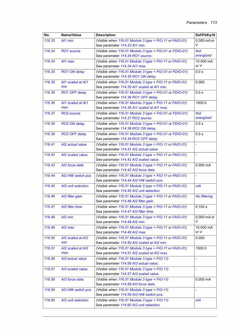
Parameters 113
116.33 AI1 min (Visible when 116.01 Module 3 type = FIO-11 or FAIO-01)See parameter 114.33 AI1 min.
0.000 mA or V
116.34 RO1 source (Visible when 116.01 Module 3 type = FIO-01 or FDIO-01)See parameter 114.34 RO1 source.
Not energized
116.34 AI1 max (Visible when 116.01 Module 3 type = FIO-11 or FAIO-01)See parameter 114.34 AI1 max.
10.000 mA or V
116.35 RO1 ON delay (Visible when 116.01 Module 3 type = FIO-01 or FDIO-01)See parameter 114.35 RO1 ON delay.
0.0 s
116.35 AI1 scaled at AI1 min
(Visible when 116.01 Module 3 type = FIO-11 or FAIO-01)See parameter 114.35 AI1 scaled at AI1 min.
0.000
116.36 RO1 OFF delay (Visible when 116.01 Module 3 type = FIO-01 or FDIO-01)See parameter 114.36 RO1 OFF delay.
0.0 s
116.36 AI1 scaled at AI1 max
(Visible when 116.01 Module 3 type = FIO-11 or FAIO-01)See parameter 114.36 AI1 scaled at AI1 max.
1500.0
116.37 RO2 source (Visible when 116.01 Module 3 type = FIO-01 or FDIO-01)See parameter 114.37 RO2 source.
Not energized
116.38 RO2 ON delay (Visible when 116.01 Module 3 type = FIO-01 or FDIO-01)See parameter 114.38 RO2 ON delay.
0.0 s
116.39 RO2 OFF delay (Visible when 116.01 Module 3 type = FIO-01 or FDIO-01)See parameter 114.39 RO2 OFF delay.
0.0 s
116.41 AI2 actual value (Visible when 116.01 Module 3 type = FIO-11 or FAIO-01)See parameter 114.41 AI2 actual value.
-
116.42 AI2 scaled value (Visible when 116.01 Module 3 type = FIO-11 or FAIO-01)See parameter 114.42 AI2 scaled value.
-
116.43 AI2 force data (Visible when 116.01 Module 3 type = FIO-11 or FAIO-01)See parameter 114.43 AI2 force data.
0.000 mA
116.44 AI2 HW switch pos (Visible when 116.01 Module 3 type = FIO-11 or FAIO-01)See parameter 114.44 AI2 HW switch pos.
-
116.45 AI2 unit selection (Visible when 116.01 Module 3 type = FIO-11 or FAIO-01)See parameter 114.45 AI2 unit selection.
mA
116.46 AI2 filter gain (Visible when 116.01 Module 3 type = FIO-11 or FAIO-01)See parameter 114.46 AI2 filter gain.
No filtering
116.47 AI2 filter time (Visible when 116.01 Module 3 type = FIO-11 or FAIO-01)See parameter 114.47 AI2 filter time.
0.100 s
116.48 AI2 min (Visible when 116.01 Module 3 type = FIO-11 or FAIO-01)See parameter 114.48 AI2 min.
0.000 mA or V
116.49 AI2 max (Visible when 116.01 Module 3 type = FIO-11 or FAIO-01)See parameter 114.49 AI2 max.
10.000 mA or V
116.50 AI2 scaled at AI2 min
(Visible when 116.01 Module 3 type = FIO-11 or FAIO-01)See parameter 114.50 AI2 scaled at AI2 min.
0.000
116.51 AI2 scaled at AI2 max
(Visible when 116.01 Module 3 type = FIO-11 or FAIO-01)See parameter 114.51 AI2 scaled at AI2 max.
1500.0
116.56 AI3 actual value (Visible when 116.01 Module 3 type = FIO-11)See parameter 114.56 AI3 actual value.
-
116.57 AI3 scaled value (Visible when 116.01 Module 3 type = FIO-11)See parameter 114.57 AI3 scaled value.
-
116.58 AI3 force data (Visible when 116.01 Module 3 type = FIO-11)See parameter 114.58 AI3 force data.
0.000 mA
116.59 AI3 HW switch pos (Visible when 116.01 Module 3 type = FIO-11)See parameter 114.59 AI3 HW switch pos.
-
116.60 AI3 unit selection (Visible when 116.01 Module 3 type = FIO-11)See parameter 114.60 AI3 unit selection.
mA
No. Name/Value Description Def/FbEq16
114 Parameters
116.61 AI3 filter gain (Visible when 116.01 Module 3 type = FIO-11)See parameter 114.61 AI3 filter gain.
No filtering
116.62 AI3 filter time (Visible when 116.01 Module 3 type = FIO-11)See parameter 114.62 AI3 filter time.
0.100 s
116.63 AI3 min (Visible when 116.01 Module 3 type = FIO-11)See parameter 114.63 AI3 min.
0.000 mA or V
116.64 AI3 max (Visible when 116.01 Module 3 type = FIO-11)See parameter 114.64 AI3 max.
10.000 mA or V
116.65 AI3 scaled at AI3 min
(Visible when 116.01 Module 3 type = FIO-11)See parameter 114.65 AI3 scaled at AI3 min.
0.000
116.66 AI3 scaled at AI3 max
(Visible when 116.01 Module 3 type = FIO-11)See parameter 114.66 AI3 scaled at AI3 max.
1500.0
116.71 AO force selection (Visible when 116.01 Module 3 type = FIO-11 or FAIO-01)See parameter 114.71 AO force selection.
00000000h
116.76 AO1 actual value (Visible when 116.01 Module 3 type = FIO-11 or FAIO-01)See parameter 114.76 AO1 actual value.
-
116.77 AO1 source (Visible when 116.01 Module 3 type = FIO-11 or FAIO-01)See parameter 114.77 AO1 source.
Zero
116.78 AO1 force data (Visible when 116.01 Module 3 type = FIO-11 or FAIO-01)See parameter 114.78 AO1 force data.
0.000 mA
116.79 AO1 filter time (Visible when 116.01 Module 3 type = FIO-11 or FAIO-01)See parameter 114.79 AO1 filter time.
0.100 s
116.80 AO1 source min (Visible when 116.01 Module 3 type = FIO-11 or FAIO-01)See parameter 114.80 AO1 source min.
0.0
116.81 AO1 source max (Visible when 116.01 Module 3 type = FIO-11 or FAIO-01)See parameter 114.81 AO1 source max.
1500.0
116.82 AO1 out at AO1 src min
(Visible when 116.01 Module 3 type = FIO-11 or FAIO-01)See parameter 114.82 AO1 out at AO1 src min.
0.000 mA
116.83 AO1 out at AO1 src max
(Visible when 116.01 Module 3 type = FIO-11 or FAIO-01)See parameter 114.83 AO1 out at AO1 src max.
20.000 mA
116.86 AO2 actual value (Visible when 116.01 Module 3 type = FAIO-01)See parameter 114.86 AO2 actual value.
-
116.87 AO2 source (Visible when 116.01 Module 3 type = FAIO-01)See parameter 114.87 AO2 source.
Zero
116.88 AO2 force data (Visible when 116.01 Module 3 type = FAIO-01)See parameter 114.88 AO2 force data.
0.000 mA
116.89 AO2 filter time (Visible when 116.01 Module 3 type = FAIO-01)See parameter 114.89 AO2 filter time.
0.100 s
116.90 AO2 source min (Visible when 116.01 Module 3 type = FAIO-01)See parameter 114.90 AO2 source min.
0.0
116.91 AO2 source max (Visible when 116.01 Module 3 type = FAIO-01)See parameter 114.91 AO2 source max.
100.0
116.92 AO2 out at AO2 src min
(Visible when 116.01 Module 3 type = FAIO-01)See parameter 114.92 AO2 out at AO2 src min.
0.000 mA
116.93 AO2 out at AO2 src max
(Visible when 116.01 Module 3 type = FAIO-01)See parameter 114.93 AO2 out at AO2 src max.
10.000 mA
119119 Operation mode Selection of external control location sources and operating
modes.
119.01 Actual operation mode
Displays the operation mode currently in use.
This parameter is read-only.
DC control
DC control DC control. 1
Power control Active power control. 2
No. Name/Value Description Def/FbEq16

Parameters 115
AC control AC voltage control. 3
119.11 Ext1/Ext2 selection Selects the source for external control location EXT1/EXT2 selection.
0 = EXT11 = EXT2
EXT1
EXT1 EXT1. 0
EXT2 EXT2. 1
MCW bit11: Ext ctrl loc
106.01 Main control word (page 72), bit 11. 2
DI1 Digital input DI1 (110.02 DI delayed status, bit 0). 3
DI2 Digital input DI2 (110.02 DI delayed status, bit 1). 4
DI3 Digital input DI3 (110.02 DI delayed status, bit 2). 5
DI4 Digital input DI4 (110.02 DI delayed status, bit 3). 6
DI5 Digital input DI5 (110.02 DI delayed status, bit 4). 7
DI6 Digital input DI6 (110.02 DI delayed status, bit 5). 8
DIO1 Digital input/output DIO1 (111.02 DIO delayed status, bit 0). 11
Other Source selection (see Terms and abbreviations on page 59). -
119.12 Ext1 ctrl mode1 Selects the operating mode 1 for external control location EXT1.
DC control
DC control DC control. 1
Power control Active power control. 2
AC control AC voltage control. 3
119.14 Ext2 ctrl mode1 Selects the operating mode 1 for external control location EXT2.
For the selections, see parameter 119.12 Ext1 ctrl mode1.
DC control
119.16 Local ctrl mode Selects the control mode for local control.
Note: This parameter cannot be changed while the IGBT supply unit is running.
DC control
DC control DC control. 1
Power control Active power control. 2
AC control AC voltage control. 3
119.17 Local control disable
Enables/disables local control. If you disable the local control, you can not use the Loc/Rem key of the panel for changing to local control.
WARNING! Before disabling local control, ensure that the control panel is not needed for stopping the IGBT supply unit.
No
No Local control enabled. 0
Yes Local control disabled. 1
120120 Start/stop Start/stop and run/start enable signal source selection;
charging settings.For information on control locations, see section Local control vs. external control (page 18).
120.01 Ext1 commands Selects the source of start and stop commands for external control location 1 (EXT1).
Note: This parameter can not be changed while the IGBT supply unit is running.
See also parameters 120.02…120.04.
In1 Start
Not sel No start or stop command sources selected. 0
No. Name/Value Description Def/FbEq16

116 Parameters
In1 Start The source of the start and stop commands is selected by parameter 120.03 Ext1 in1 source. The state transitions of the source bits are interpreted as follows:
1
In1P Start; In2 Stop The sources of the start and stop commands are selected by parameters 120.03 Ext1 in1 source and 120.04 Ext1 in2 source. The state transitions of the source bits are interpreted as follows:
Notes:
• Parameter 120.02 Ext1 start trigger type has no effect with this setting.
• When source 2 is 0, the Start and Stop keys on the control panel are disabled.
4
Fieldbus A The start and stop commands are taken from fieldbus adapter A.
12
D2D link The start and stop commands are taken from another drive through the D2D (Drive-to-drive) link.
15
DDCS controller The start and stop commands are taken from an external (DDCS) controller.
16
Application Program The start and stop commands are taken from the application program control word.
21
ATF Reserved. 22
120.02 Ext1 start trigger type
Defines whether the start signal for external control location EXT1 is edge-triggered or level-triggered.
Note: This parameter is not effective if a pulse-type start signal is selected. See the descriptions of the selections of parameter 120.01 Ext1 commands.
Edge
Edge The start signal is edge-triggered. 0
Level The start signal is level-triggered. 1
120.03 Ext1 in1 source Selects source 1 for parameter 120.01 Ext1 commands. DI2
Off 0. 0
On 1. 1
DI1 Digital input DI1 (110.02 DI delayed status, bit 0). 2
DI2 Digital input DI2 (110.02 DI delayed status, bit 1). 3
DI3 Digital input DI3 (110.02 DI delayed status, bit 2). 4
DI4 Digital input DI4 (110.02 DI delayed status, bit 3). 5
DI5 Digital input DI5 (110.02 DI delayed status, bit 4). 6
DI6 Digital input DI6 (110.02 DI delayed status, bit 5). 7
DIO1 Digital input/output DIO1 (111.02 DIO delayed status, bit 0). 10
DIO2 Digital input/output DIO2 (111.02 DIO delayed status, bit 1). 11
Other Source selection (see Terms and abbreviations on page 59). -
120.04 Ext1 in2 source Selects source 2 for parameter 120.01 Ext1 commands.
For the available selections, see parameter 120.03 Ext1 in1 source.
Off
No. Name/Value Description Def/FbEq16
State of source 1 (120.03) Command0 -> 1 (120.02 = Edge)
1 (120.02 = Level)Start
0 Stop
State of source 1 (120.03)
State of source 2 (120.04) Command
0 -> 1 1 StartAny 0 Stop
Parameters 117
120.06 Ext2 commands Selects the source of start and stop commands for external control location 2 (EXT2).
See also parameters 120.07…120.09.
Not sel
Not sel No start or stop command sources selected. 0
In1 Start The source of the start and stop commands is selected by parameter 120.08 Ext2 in1 source. The state transitions of the source bits are interpreted as follows:
1
In1P Start; In2 Stop The sources of the start and stop commands are selected by parameters 120.08 Ext2 in1 source and 120.09 Ext2 in2 source. The state transitions of the source bits are interpreted as follows:
Notes:
• Parameter 120.07 Ext2 start trigger type has no effect with this setting.
• When source 2 is 0, the Start and Stop keys on the control panel are disabled.
4
Keypad The start and stop commands are taken from the control panel (or PC connected to the control panel).
11
Fieldbus A The start and stop commands are taken from fieldbus adapter A.
12
D2D link The start and stop commands are taken from another drive through the D2D (Drive-to-drive) link.
15
DDCS controller The start and stop commands are taken from an external (DDCS) controller.
16
Application Program The start and stop commands are taken from the application program control word.
21
ATF Reserved. 22
120.07 Ext2 start trigger type
Defines whether the start signal for external control location EXT2 is edge-triggered or level-triggered.
Note: In case the settings of parameters 120.06 and 120.07 are in conflict, the setting of parameter 120.06 takes preference.
Edge
Edge The start signal is edge-triggered. 0
Level The start signal is level-triggered. 1
120.08 Ext2 in1 source Selects source 1 for parameter 120.06 Ext2 commands.
For the available selections, see parameter 120.03 Ext1 in1 source.
Off
120.09 Ext2 in2 source Selects source 2 for parameter 120.06 Ext2 commands.
For the available selections, see parameter 120.03 Ext1 in1 source.
Off
No. Name/Value Description Def/FbEq16
State of source 1 (120.08) Command0 -> 1 (120.07 = Edge)
1 (120.07 = Level)Start
0 Stop
State of source 1 (120.08)
State of source 2 (120.09) Command
0 -> 1 1 StartAny 0 Stop
118 Parameters
120.12 Run enable 1 source
Selects the source of the external run enable signal. If the run enable signal is switched off, the IGBT supply unit will not start, or stops if running.
1 = Run enable.
Note: This parameter cannot be changed while the IGBT supply unit is running.
DI2
Off 0 (off). 0
On 1 (on). 1
DI1 Digital input DI1 (110.02 DI delayed status, bit 0). 2
DI2 Digital input DI2 (110.02 DI delayed status, bit 1). 3
DI3 Digital input DI3 (110.02 DI delayed status, bit 2). 4
DI4 Digital input DI4 (110.02 DI delayed status, bit 3). 5
DI5 Digital input DI5 (110.02 DI delayed status, bit 4). 6
DI6 Digital input DI6 (110.02 DI delayed status, bit 5). 7
DIO1 Digital input/output DIO1 (111.02 DIO delayed status, bit 0). 10
DIO2 Digital input/output DIO2 (111.02 DIO delayed status, bit 1). 11
Other Source selection (see Terms and abbreviations on page 59). -
120.19 Enable start command
Selects the source for the start enable signal.
1 = Start enable.
With the signal switched off, the IGBT supply unit will not start. (Switching the signal off while the IGBT supply unit is running will not stop the IGBT supply unit.)
On
Off 0 (off). 0
On 1 (on). 1
DI1 Digital input DI1 (110.02 DI delayed status, bit 0). 2
DI2 Digital input DI2 (110.02 DI delayed status, bit 1). 3
DI3 Digital input DI3 (110.02 DI delayed status, bit 2). 4
DI4 Digital input DI4 (110.02 DI delayed status, bit 3). 5
DI5 Digital input DI5 (110.02 DI delayed status, bit 4). 6
DI6 Digital input DI6 (110.02 DI delayed status, bit 5). 7
DIO1 Digital input/output DIO1 (111.02 DIO delayed status, bit 0). 10
DIO2 Digital input/output DIO2 (111.02 DIO delayed status, bit 1). 11
Other Source selection (see Terms and abbreviations on page 59). -
120.21 Delay for MCB DI3 supervision
Start and stop delay for supervision of main circuit breaker DI3 feedback in external charging. After the delay a fault is given in start and stop states if the command and the feedback do not match.
1.00 s
0.00…8.00 s Start and stop delay for supervision of main circuit breaker DI3 feedback.
100 = 1 s
120.22 Max current for MCB closing
Defines the maximum charging current for the charging function. When the charging current is below the value defined with this parameter, the main circuit breaker can be closed. (It will be closed only if also the remaining criteria is met.) The limit is given as a percent value of the nominal current of the supply unit. See also section Charging on page 41. 10% = 10% of the nominal current.
5%
0…10% Current value in percent. 1 = 1%
120.23 Max DC charging time
Defines the maximum charging time for the charging function. See section Charging on page 41.
3.00 s
0.00…10.00 s Maximum charging time 100 = 1 s
No. Name/Value Description Def/FbEq16

Parameters 119
120.25 MCB closing level Defines the DC link voltage level for the charging function. When the measured DC link voltage exceeds the level, the main contactor/breaker can be closed. 100% equals to the value of parameter 101.62 Nominal DC voltage. See section Charging on page 41.
80%
20…100% Intermediate circuit DC voltage level in percent of the nominal 1 = 1%
120.26 Maximum dU/dt Defines the maximum DC link voltage change rate (dU/dt) for the charging function. When the change rate falls below this maximum change rate limit, the control program can close the main contactor/breaker. The change rate is measured in 10 ms sample interval. See section Charging on page 41.
50.0 V/s
0.0…200.0 V/s Maximum dU/dt change. 1 = 1 V/s
120.27 Start delay Defines the start delay that delay the setting of the charged state after the main circuit breaker has closed. Without charged state the start command is blocked from the modulator.
0.50 s
0.00…10.00 s Start delay. 100 = 1 s
120.28 MCB relay timing Defines the time for how long the MCB relay is closed/open in parallel with the charging relay. Positive time means that both relays are kept opened that time. Negative time means that both relays are kept closed at the same time. See picture in section Charging on page 41.
-0.10 s
-6.00…6.00 s Time between charging contactor opening and main circuit contactor closing.
100 = 1 s
120.29 Diode mode Enables diode mode, when additional charging circuit is in use and the unit acts as a pure diode bridge. Diode mode blocks the start command for modulator after charging. In diode mode, the modulation is stopped and the main contactor is closed. Using diode mode reduces the number of main contactor operations.
Off
Off Diode mode is disabled. 0
On Diode mode is enabled. 1
DI1 Digital input DI1 (110.02 DI delayed status, bit 0). 2
DI2 Digital input DI2 (110.02 DI delayed status, bit 1). 3
DI3 Digital input DI3 (110.02 DI delayed status, bit 2).
Note: DI3 is reserved for main breaker/contactor fault in the control program. Do not select it for any other use.
4
DI4 Digital input DI4 (110.02 DI delayed status, bit 3). 5
DI5 Digital input DI5 (110.02 DI delayed status, bit 4). 6
DI6 Digital input DI6 (110.02 DI delayed status, bit 5). 7
DIO1 Digital input/output DIO1 (111.02 DIO delayed status, bit 0). 10
DIO2 Digital input/output DIO2 (111.02 DIO delayed status, bit 1). 11
Other Source selection (see Terms and abbreviations on page 59). -
120.30 External charge enable
Enables the charging function. See section Charging on page 41.
Yes
No External charging disabled. 0
Yes External charging enabled. 1
120.50 Charging overload event sel
Selects the event type for charging overload event. See section Charging on page 41.
Fault
Fault The supply unit trips on fault 3E09 Charging count. 0
Warning The supply unit generates a warning AE85 Charging count. 1
No action No action taken. 2
No. Name/Value Description Def/FbEq16

120 Parameters
121121 Start/stop mode Emergency stop settings.
121.04 Emergency stop mode
Selects the way the IGBT supply unit is stopped when an emergency stop command is received. The source of the emergency stop signal is selected with parameter 121.05 Emergency stop source.
Stop and warning
Stop and warning Stop IGBT supply unit and show emergency stop warning. 0
Warning Show emergency stop warning but do not stop IGBT supply unit.
1
Fault Stop IGBT supply unit and create an emergency stop fault. 2
121.05 Emergency stop source
Selects the source of the emergency stop signal.
0 = Emergency stop active1 = Emergency stop command is off, normal operation
Note: This parameter cannot be changed while the IGBT supply unit is running.
Inactive (true)
Active (false) 0 (emergency stop command is on). 0
Inactive (true) 1 (emergency stop command is off). 1
DIIL DIIL input (110.02 DI delayed status, bit 15). 2
DI1 Digital input DI1 (110.02 DI delayed status, bit 0). 3
DI2 Digital input DI2 (110.02 DI delayed status, bit 1). 4
DI3 Digital input DI3 (110.02 DI delayed status, bit 2).
Note: DI3 is reserved for main breaker/contactor fault in the control program. Do not select it for any other use.
5
DI4 Digital input DI4 (110.02 DI delayed status, bit 3). 6
DI5 Digital input DI5 (110.02 DI delayed status, bit 4). 7
DI6 Digital input DI6 (110.02 DI delayed status, bit 5). 8
DIO1 Digital input/output DIO1 (111.02 DIO delayed status, bit 0). 11
DIO2 Digital input/output DIO2 (111.02 DIO delayed status, bit 1). 12
Other Source selection (see Terms and abbreviations on page 59). -
122122 Power reference Settings of the active power reference chain.
See the control chain diagrams in chapter Control chain diagrams (page 263).
122.01 User Power ref Defines the active power reference value for selection User ref of the parameter 122.02 Power ref sel. The unit is selected with parameter 122.06 Power ref type. See the diagram Power reference chain (page 265).
-
- The active power reference value. 1 = 1
122.02 Power ref sel Selects the source for active power reference. See the diagram Power reference chain (page 265).
User ref
User ref 122.01 User Power ref. 0
AI1 scaled 112.12 AI1 scaled value (see page 87). 1
AI2 scaled 112.22 AI2 scaled value (see page 88). 2
Panel Control panel. 3
FB A ref1 Fieldbus adapter A reference 1. 4
FB A ref2 Fieldbus adapter A reference 2. 5
DDCS ctrl ref1 103.11 DDCS controller ref 1 (see page 65). 10
DDCS ctrl ref2 103.12 DDCS controller ref 2 (see page 65). 11
Other The value is taken from another parameter. (See Terms and abbreviations on page 59.)
-
No. Name/Value Description Def/FbEq16
Parameters 121
122.03 Power ref 1 Shows the unscaled power reference value selected by 122.02 Power ref sel. See the diagram Power reference chain (page 265).
-
- The unscaled power reference value. 1 = 1
122.04 Power ref scale Defines the scaling factor for 122.03 Power ref 1. See the diagram Power reference chain (page 265).
1.00
-1000.00 …1000.00 The scaling factor. 1 = 1
122.05 Power ref 2 Shows the scaled power reference value: the value selected by parameter 122.02 Power ref sel and multiplied by parameter 122.04 Power ref scale. See the diagram Power reference chain (page 265).
1 = 1
122.06 Power ref type Selects the active power reference type for the scaled reference value (parameter 122.05 Power ref 2). See the diagram Power reference chain (page 265).
Ipow ref [A]
Ipow ref [A] Active current reference in Amperes. 0
Ipow ref [%] Active current reference in percent of the nominal current. 1
Pow ref kW Active power reference in kW. 2
Pow ref % Active power reference in percent of the nominal power. 3
122.07 Ipower ref % Shows the active current reference in percent of the nominal current of the converter. See the diagram Power reference chain (page 265).
-
-1000.0 …1000.0 % Power reference in percent. 1 = 1%
122.08 Ipower ref Shows the active current reference in Amperes. See the diagram Power reference chain (page 265).
-
- Active current reference. 1 = 1 A
122.09 Power ref % Shows the power reference in percent of the nominal power. See the diagram Power reference chain (page 265).
-
-1000.0 …1000.0 % Power reference in percent. 1 = 1%
122.10 Power ref Shows the power reference in kW. See the diagram Power reference chain (page 265).
-
- Power reference in kW. 1 = 1 kW
122.11 Ipower ref max % Defines the maximum limit for the active current reference in percent. See the diagram Power reference chain (page 265).
100.0%
0.0 …200.0% Maximum active current reference in percent. 1 = 1%
122.12 Ipower ref min % Defines the minimum limit for the active current reference in percent. See the diagram Power reference chain (page 265).
-100.0%
-200.0…0.0% Minimum active current reference in percent. 1 = 1%
122.13 Ipower ref lim % Shows the limited active current reference. Limitation is based on 122.11 Ipower ref max % and 122.12 Ipower ref min % values. See the diagram Power reference chain (page 265).
-
-200.0…200.0% Output value of active power reference limitation. 1 = 1%
122.14 Ipower ref ramp up Defines the active current ramp up time (time from zero to nominal) in ms. See the diagram Power reference chain (page 265).
1000 ms
0…30000 ms Active current ramp up time. 1 = 1 ms
122.15 Ipower ref ramp down
Defines the active current ramp down time (time from nominal to zero) in ms. See the diagram Power reference chain (page 265).
1000 ms
0…30000 ms Active current ramp down time. 1 = 1 ms
122.16 Ipower ref out % Shows the output value of active current reference in percent for the controller. See the diagram Power reference chain (page 265).
-
-200.0…200.0% Output value of active current reference. 1 = 1%
No. Name/Value Description Def/FbEq16

122 Parameters
122.17 Ipower ref out Shows the output value of active current reference in Amperes for the controller. If the reference can not be met, an actual value is used in the signal instead of ramped value. See the diagram Power reference chain (page 265).
-
- Output value of active current reference. 1 = 1 A
122.18 Power ref out % Shows the output value of active power reference in percent of the nominal power for the controller. See the diagram Power reference chain (page 265).
-
-200.0…200.0% Output value of active power reference. 1 = 1%
122.19 Power ref out Shows the output value of active power reference in kW for the controller. See the diagram Power reference chain (page 265).
-
- Output value of active power reference. 1 = 1 kW
123123 DC voltage reference Settings of the DC voltage reference chain.
See the control chain diagrams in chapter Control chain diagrams (page 263).
123.01 User DC voltage ref Defines the DC voltage reference value for selection User ref of the parameter 123.02 DC voltage ref selection. See the diagram DC voltage reference chain (page 264).
-
0.00 … 2000.00 V DC voltage reference value. 0 = 1 V
123.02 DC voltage ref selection
Selects the control location for DC voltage reference. See the diagram DC voltage reference chain (page 264).
User ref
User ref 123.01 User DC voltage ref. 0
AI1 scaled 112.12 AI1 scaled value (see page 87). 1
AI2 scaled 112.22 AI2 scaled value (see page 88). 2
Panel Control panel. 3
FB A ref1 Fieldbus adapter A reference 1. 4
FB A ref2 Fieldbus adapter A reference 2. 5
DDCS ctrl ref1 103.11 DDCS controller ref 1 (see page 65). 10
DDCS ctrl ref2 103.12 DDCS controller ref 2 (see page 65). 11
Other The value is taken from another parameter. (See Terms and abbreviations on page 59.)
-
123.03 DC voltage ref 1 Shows the unscaled DC voltage reference value selected by 123.02 DC voltage ref selection. See the diagram DC voltage reference chain (page 264).
-
0.00 … 2000.00 V Value of the DC voltage reference. 1 = 1 V
123.05 DC voltage ref 2 Shows the scaled DC reference value (123.03 DC voltage ref 1 × 123.12 DC voltage ref scale). See the diagram DC voltage reference chain (page 264).
-
0.00 … 2000.00 V Limitation of DC voltage reference. 1 = 1 V
123.06 DC voltage ref max Maximum value of DC voltage reference in Volts. The maximum DC voltage reference is approximately113% × sqrt(2) × 195.01 Supply voltage (the high value).
This parameter is an overvoltage controller activation limit in power control mode (maximum value 123.50 Overvoltage trip limit - 50 V).
See the diagram DC voltage reference chain (page 264), and section Boost limits on page 37.
1200 V
0 … 2000 V Maximum DC voltage reference. 1 = 1 V
No. Name/Value Description Def/FbEq16

Parameters 123
123.07 DC voltage ref min Minimum value of DC voltage reference in Volts. This parameter is an undervoltage controller activation limit in power control mode.
See the diagram DC voltage reference chain (page 264).
200 V
0 …1100 V Minimum DC voltage reference. 1 = 1 V
123.08 DC voltage ref lim Output value of DC voltage reference limitation. Limitation is based on 123.06 DC voltage ref max and 123.07 DC voltage ref min values. If the reference and minimum limit cannot be met (diodes keep the DC voltage level higher), an actual value is used in the signal instead of minimum limit value. See the diagram DC voltage reference chain (page 264).
-
0.00 … 2000.00 V Output value of DC voltage reference limitation. 1 = 1 V
123.09 DC voltage ref ramp up
DC voltage reference ramp up time (time from zero to nominal DC level) in ms. See the diagram DC voltage reference chain (page 264).
1000 ms
0…10000 ms DC voltage reference ramp up time. 1 = 1 ms
123.10 DC voltage ref ramp down
DC voltage reference ramp down time (time from nominal DC level to zero) in ms. See the diagram DC voltage reference chain (page 264).
1000 ms
0…10000 ms DC voltage reference ramp down time. 1 = 1 ms
123.11 DC voltage ref out Output value of DC voltage reference ramping in Volts for the controller. If the reference can not be met, an actual value is used in the signal instead of ramped value. See the diagram DC voltage reference chain (page 264).
-
0.00 … 2000.00 V Output value of DC voltage reference ramping. 1 = 1 V
123.12 DC voltage ref scale DC voltage reference scaling factor. See the diagram DC voltage reference chain (page 264).
1.00
-100.00…100.00 DC voltage reference scaling factor.
123.13 DC voltage ref add Defines the addition value to DC voltage reference (parameter 123.03 DC voltage ref 1). See the diagram DC voltage reference chain (page 264).
0.000 V
-30.000…30.000 V Addition value. 1000 = 1 V
123.30 Udc-ctrl droop Disables/enables the power share between two supply units that are fed from separate transformers but are connected to same DC bus. See section Power share with droop control on page 49.
Disabled
Disabled Disabled. 0
Enabled Enabled. 1
123.31 Udc-ctrl drooping rate
Defines the drooping rate in percent. See parameter 123.30 Udc-ctrl droop, and section Power share with droop control on page 49.
5.0%
0.0…100.0% Drooping rate. 1 = 1%
123.32 Master power Defines the power of the master unit in master/follower set-up.
0.00
-2000.00…2000.00 Power of the master unit. 1 = 10
124124 Reactive power reference
Settings of the reactive power reference chain.See the control chain diagrams in chapter Control chain diagrams (page 263).
124.01 User Qref Defines the reactive power reference value for the selection User ref of parameter 124.02 Q power ref selection. The unit is selected with parameter 124.06 Q power ref type. See the diagram Reactive power reference chain (page 266).
0
- Reactive power reference value 1 = 1
No. Name/Value Description Def/FbEq16

124 Parameters
124.02 Q power ref selection
Selects the control location for reactive power reference. See the diagram Reactive power reference chain (page 266).
-
User ref Value of parameter 124.01 User Qref. 0
AI1 scaled 112.12 AI1 scaled value (see page 87). 1
AI2 scaled 112.22 AI2 scaled value (see page 88). 2
Panel Control panel. 3
FB A ref1 Fieldbus adapter A reference 1. 4
FB A ref2 Fieldbus adapter A reference 2. 5
ABB ctrl ref2 Reserved. 10
D2D or M/F (IDL) ref1
Reserved. 11
Other The value is taken from another parameter. (See Terms and abbreviations on page 59.)
-
124.03 Qref 1 Shows the reference value selected by 124.01 User Qref or 124.02 Q power ref selection. See the diagram Reactive power reference chain (page 266).
1 = 1
124.04 Q ref scale Defines the scaling factor for 124.03 Qref 1. See the diagram Reactive power reference chain (page 266).
1.00
-1000.00 …1000.00 The scaling factor. 1 = 1
124.05 Qref 2 Shows the reference value (124.03 Qref 1) after scaling. See the diagram Reactive power reference chain (page 266).
1
- The scaled value. 1 = 1
124.06 Q power ref type Selects the reactive power reference type and unit. See the diagram Reactive power reference chain (page 266).
Ireact ref [A]
Ireact ref [A] Reactive current reference in Amperes. 0
Ireact ref [%] Reactive current reference in % of the nominal current. 1
Qref [kVAr] Reactive power reference in kVAr. 2
Qref [%] Reactive power reference in % of nominal power. 3
Phi Reactive power reference angle in degrees 1 = 1degree. The range is limited to -30° … 30°.
4
CosPhi Reactive power reference in cosphi 0.9 = 0.9 capacitive. The range is limited to -0.86 … -1 and 0.86 … 1.
5
Q(x) regulation curve
Q(x) regulation curve. 8
124.07 Ireact ref % Shows the reactive current reference in percent. See the diagram Reactive power reference chain (page 266).
-
-1000.0 …1000.0 % Reactive current reference in percent. 1 = 1%
124.08 Ireact ref Shows the reactive current reference in Amperes. See the diagram Reactive power reference chain (page 266).
-
- Reactive current reference. 1 = 1 A
124.09 Q power ref % Shows the reactive power reference in percent of the nominal power. See the diagram Reactive power reference chain (page 266).
-
-1000.0 …1000.0 % Reactive power reference in percent. 1 = 1%
124.10 Q power ref Shows the reactive power reference in kVAr. See the diagram Reactive power reference chain (page 266).
-
- Reactive power reference in kVAr. 1 = 1 kVAr
124.11 Ireact ref max % Defines the maximum limit for the reactive power reference in percent. See the diagram Reactive power reference chain (page 266).
80.0%
0.0 …200.0% Maximum reactive current reference in percent. 1 = 1%
No. Name/Value Description Def/FbEq16

Parameters 125
124.12 Ireact ref min % Defines the minimum limit for the reactive power reference in percent. See the diagram Reactive power reference chain (page 266).
-80.0%
-200.0…0.0% Minimum reactive current reference in percent. 1 = 1%
124.13 Ireact ref lim % Output value of reactive power reference limitation. Limitation is based on 124.11 Ireact ref max % and 124.12 Ireact ref min % values. See the diagram Reactive power reference chain (page 266).
-
-200.0…200.0% Output value of reactive power reference limitation. 1 = 1%
124.14 Ireact ref ramp up Defines the reactive current ramp up time (time from zero to nominal current) in ms. See the diagram Reactive power reference chain (page 266).
1000 ms
0…30000 ms Reactive current ramp up time. 1 = 1 ms
124.15 Ireact ref ramp down
Defines the reactive current ramp down time (time from nominal current to zero) in ms. See the diagram Reactive power reference chain (page 266).
1000 ms
0…30000 ms Reactive current ramp down time. 1 = 1 ms
124.16 Ireact ref out % Shows the output value of reactive current reference in percent for the controller. See the diagram Reactive power reference chain (page 266).
-
-200.0…200.0% Output value of reactive current reference. 1 = 1%
124.17 Ireact ref out Shows the output value of reactive current reference in Amperes for the controller. If the reference can not be met, an actual value is used in the signal instead of ramped value. See the diagram Reactive power reference chain (page 266).
-
- Output value of reactive current reference. 1 = 1 A
124.18 Q power ref out % Shows the output value of reactive power reference in percent of the nominal power for the controller. See the diagram Reactive power reference chain (page 266).
-
-200.0…200.0% Output value of reactive power reference. 1 = 1%
124.19 Q power ref out Shows the output value of reactive power reference in kVAr for the controller. See the diagram Reactive power reference chain (page 266).
-
- Output value of reactive power reference. 1 = 1 kVAr
124.20 AC control gain Defines the relative gain of the AC voltage controller used in the reactive power reference chain. See the diagram Reactive power reference chain (page 266).
10.0
0.0…100.0 Relative gain of the AC voltage controller. 10 = 1
124.21 AC control integ time
Defines the integration time of the AC voltage controller used in the reactive power reference chain. See the diagram Reactive power reference chain (page 266).
100 ms
0…30000 ms Integration time of the AC voltage controller. 1 = 1 ms
124.22 AC diff max % Defines the maximum limit for AC voltage difference (reference - actual) used in the reactive power reference chain. See the diagram Reactive power reference chain (page 266).
10.0%
0.0…30.0% Maximum limit of AC control input. 1 = 1%
124.23 AC diff min % Defines the minimum limit for the AC voltage difference (reference - actual) used in the reactive power reference chain. See the diagram Reactive power reference chain (page 266).
-10.0%
-30.0…0.0% Minimum limit of AC control input. 1 = 1%
No. Name/Value Description Def/FbEq16
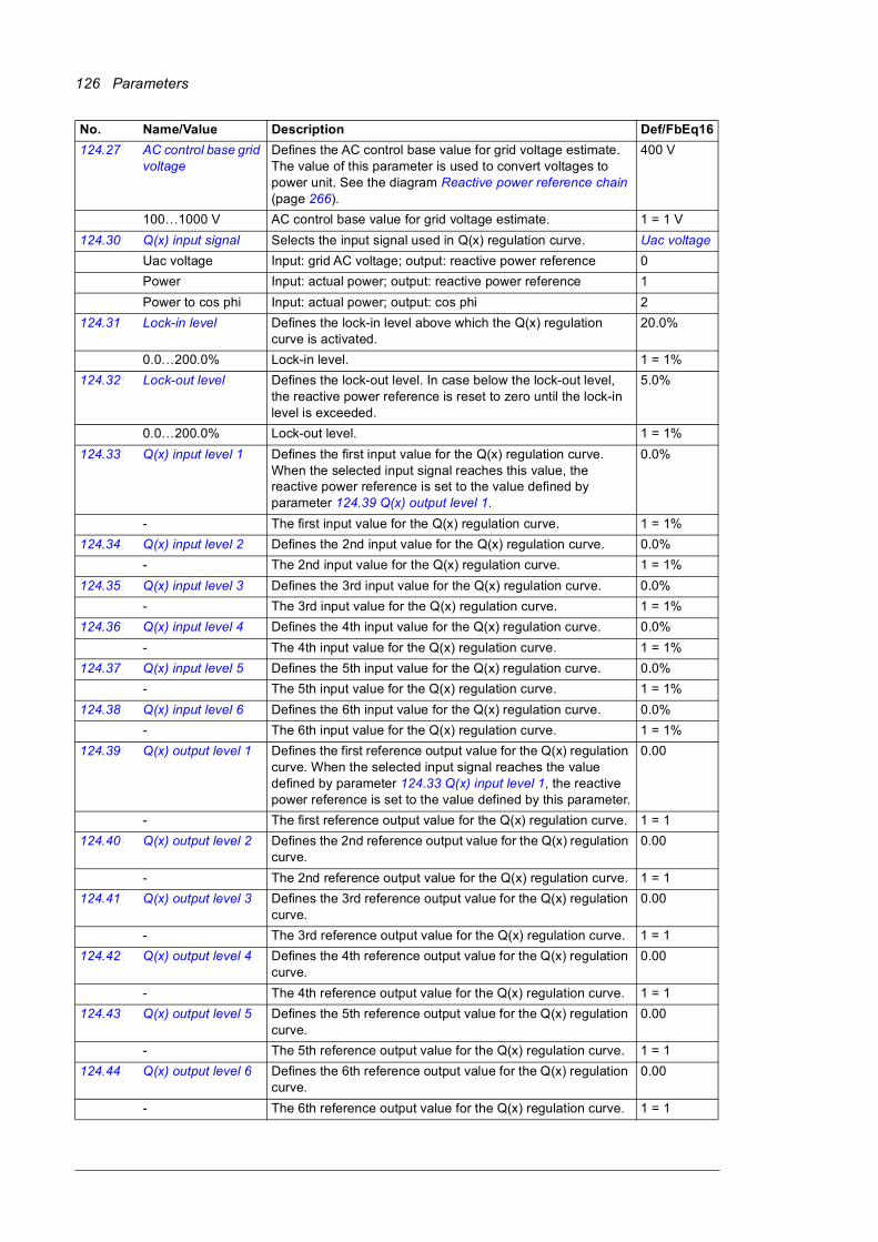
126 Parameters
124.27 AC control base grid voltage
Defines the AC control base value for grid voltage estimate. The value of this parameter is used to convert voltages to power unit. See the diagram Reactive power reference chain (page 266).
400 V
100…1000 V AC control base value for grid voltage estimate. 1 = 1 V
124.30 Q(x) input signal Selects the input signal used in Q(x) regulation curve. Uac voltage
Uac voltage Input: grid AC voltage; output: reactive power reference 0
Power Input: actual power; output: reactive power reference 1
Power to cos phi Input: actual power; output: cos phi 2
124.31 Lock-in level Defines the lock-in level above which the Q(x) regulation curve is activated.
20.0%
0.0…200.0% Lock-in level. 1 = 1%
124.32 Lock-out level Defines the lock-out level. In case below the lock-out level, the reactive power reference is reset to zero until the lock-in level is exceeded.
5.0%
0.0…200.0% Lock-out level. 1 = 1%
124.33 Q(x) input level 1 Defines the first input value for the Q(x) regulation curve. When the selected input signal reaches this value, the reactive power reference is set to the value defined by parameter 124.39 Q(x) output level 1.
0.0%
- The first input value for the Q(x) regulation curve. 1 = 1%
124.34 Q(x) input level 2 Defines the 2nd input value for the Q(x) regulation curve. 0.0%
- The 2nd input value for the Q(x) regulation curve. 1 = 1%
124.35 Q(x) input level 3 Defines the 3rd input value for the Q(x) regulation curve. 0.0%
- The 3rd input value for the Q(x) regulation curve. 1 = 1%
124.36 Q(x) input level 4 Defines the 4th input value for the Q(x) regulation curve. 0.0%
- The 4th input value for the Q(x) regulation curve. 1 = 1%
124.37 Q(x) input level 5 Defines the 5th input value for the Q(x) regulation curve. 0.0%
- The 5th input value for the Q(x) regulation curve. 1 = 1%
124.38 Q(x) input level 6 Defines the 6th input value for the Q(x) regulation curve. 0.0%
- The 6th input value for the Q(x) regulation curve. 1 = 1%
124.39 Q(x) output level 1 Defines the first reference output value for the Q(x) regulation curve. When the selected input signal reaches the value defined by parameter 124.33 Q(x) input level 1, the reactive power reference is set to the value defined by this parameter.
0.00
- The first reference output value for the Q(x) regulation curve. 1 = 1
124.40 Q(x) output level 2 Defines the 2nd reference output value for the Q(x) regulation curve.
0.00
- The 2nd reference output value for the Q(x) regulation curve. 1 = 1
124.41 Q(x) output level 3 Defines the 3rd reference output value for the Q(x) regulation curve.
0.00
- The 3rd reference output value for the Q(x) regulation curve. 1 = 1
124.42 Q(x) output level 4 Defines the 4th reference output value for the Q(x) regulation curve.
0.00
- The 4th reference output value for the Q(x) regulation curve. 1 = 1
124.43 Q(x) output level 5 Defines the 5th reference output value for the Q(x) regulation curve.
0.00
- The 5th reference output value for the Q(x) regulation curve. 1 = 1
124.44 Q(x) output level 6 Defines the 6th reference output value for the Q(x) regulation curve.
0.00
- The 6th reference output value for the Q(x) regulation curve. 1 = 1
No. Name/Value Description Def/FbEq16
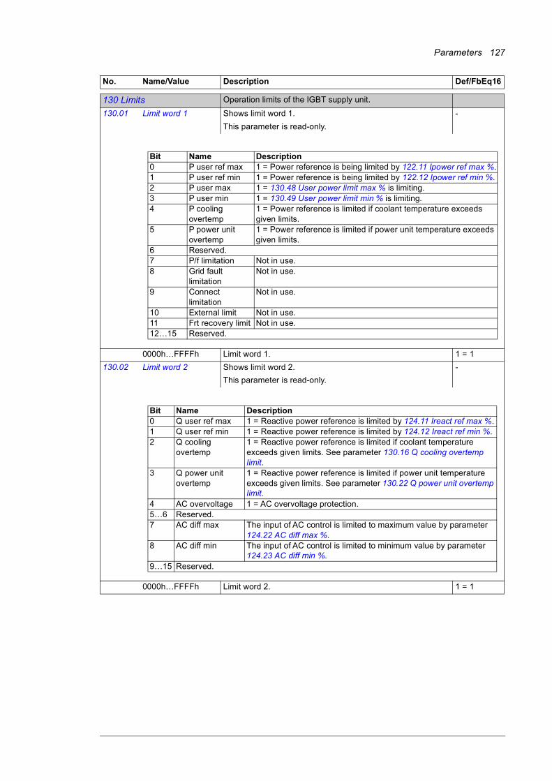
Parameters 127
130130 Limits Operation limits of the IGBT supply unit.
130.01 Limit word 1 Shows limit word 1.
This parameter is read-only.
-
0000h…FFFFh Limit word 1. 1 = 1
130.02 Limit word 2 Shows limit word 2.
This parameter is read-only.
-
0000h…FFFFh Limit word 2. 1 = 1
No. Name/Value Description Def/FbEq16
Bit Name Description0 P user ref max 1 = Power reference is being limited by 122.11 Ipower ref max %.1 P user ref min 1 = Power reference is being limited by 122.12 Ipower ref min %.2 P user max 1 = 130.48 User power limit max % is limiting.3 P user min 1 = 130.49 User power limit min % is limiting.4 P cooling
overtemp1 = Power reference is limited if coolant temperature exceeds given limits.
5 P power unit overtemp
1 = Power reference is limited if power unit temperature exceeds given limits.
6 Reserved.7 P/f limitation Not in use. 8 Grid fault
limitationNot in use.
9 Connect limitation
Not in use.
10 External limit Not in use. 11 Frt recovery limit Not in use. 12…15 Reserved.
Bit Name Description0 Q user ref max 1 = Reactive power reference is limited by 124.11 Ireact ref max %.1 Q user ref min 1 = Reactive power reference is limited by 124.12 Ireact ref min %.2 Q cooling
overtemp1 = Reactive power reference is limited if coolant temperature exceeds given limits. See parameter 130.16 Q cooling overtemp limit.
3 Q power unit overtemp
1 = Reactive power reference is limited if power unit temperature exceeds given limits. See parameter 130.22 Q power unit overtemp limit.
4 AC overvoltage 1 = AC overvoltage protection. 5…6 Reserved.7 AC diff max The input of AC control is limited to maximum value by parameter
124.22 AC diff max %.8 AC diff min The input of AC control is limited to minimum value by parameter
124.23 AC diff min %.9…15 Reserved.

128 Parameters
130.03 Limit word 3 Shows limit word 3.
This parameter is read-only.
See the diagram Current limitation chain (page 268).
-
0000h…FFFFh Limit word 3. 1 = 1
130.04 Limit word 4 Shows limit word 4.
This parameter is read-only.
-
0000h…FFFFh Limit word 4. 1 = 1
No. Name/Value Description Def/FbEq16
Bit Name Description0 undervoltage
limitUndervoltage controller limits the power.
1 overvoltage limit Overvoltage controller limits the power.2 Motoring power Power is limited by user limit or temperature limit. See parameters
130.47…130.49. 3 Generating
powerPower is limited by user limit or temperature limit. See parameters 130.47…130.49.
4 Active current limit
Active current is limited. For details, see bits 6…9 and 14…15.
5 Reactive current limit
Reactive current is limited. For details, see bits 12…13.
6 thermal limit Current is limited by main circuit thermal limit (this internal limit can not be changed by the user).
7 SOA limit Current is limited by the safe operation area (SOA) limit (this internal limit can not be changed by the user).
8 user current limit Current is limited by 130.46 Current limit %.9 thermal igbt Current is limited by maximum thermal IGBT stress (this internal
limit can not be changed by the user).10…11 Reserved.12 Q act neg Total current limitation limits negative reactive current.13 Q act pos Total current limitation limits positive reactive current.14 P act neg Total current limitation limits negative active current.15 P act pos Total current limitation limits positive active current.
Bit Name Description0 Udc ref max 1 = Udc reference is being limited by 123.06 DC voltage ref max.
1 Udc ref min 1 = Udc reference is being limited by 123.07 DC voltage ref min.
2 User I max Current is limited by 130.46 Current limit %.3 Temp I max Current is limited by temperature-based current limit.4…15 Reserved.
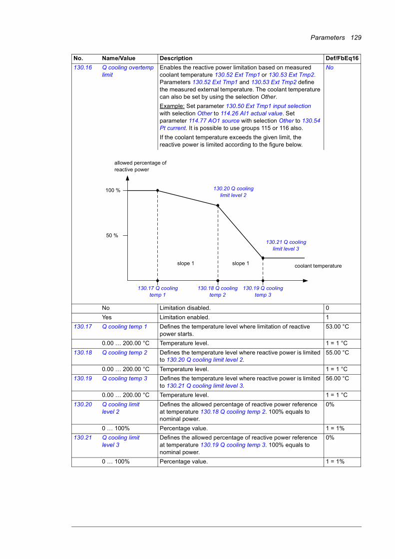
Parameters 129
130.16 Q cooling overtemp limit
Enables the reactive power limitation based on measured coolant temperature 130.52 Ext Tmp1 or 130.53 Ext Tmp2. Parameters 130.52 Ext Tmp1 and 130.53 Ext Tmp2 define the measured external temperature. The coolant temperature can also be set by using the selection Other.
Example: Set parameter 130.50 Ext Tmp1 input selection with selection Other to 114.26 AI1 actual value. Set parameter 114.77 AO1 source with selection Other to 130.54 Pt current. It is possible to use groups 115 or 116 also.
If the coolant temperature exceeds the given limit, the reactive power is limited according to the figure below.
No
No Limitation disabled. 0
Yes Limitation enabled. 1
130.17 Q cooling temp 1 Defines the temperature level where limitation of reactive power starts.
53.00 °C
0.00 … 200.00 °C Temperature level. 1 = 1 °C
130.18 Q cooling temp 2 Defines the temperature level where reactive power is limited to 130.20 Q cooling limit level 2.
55.00 °C
0.00 … 200.00 °C Temperature level. 1 = 1 °C
130.19 Q cooling temp 3 Defines the temperature level where reactive power is limited to 130.21 Q cooling limit level 3.
56.00 °C
0.00 … 200.00 °C Temperature level. 1 = 1 °C
130.20 Q cooling limit level 2
Defines the allowed percentage of reactive power reference at temperature 130.18 Q cooling temp 2. 100% equals to nominal power.
0%
0 … 100% Percentage value. 1 = 1%
130.21 Q cooling limit level 3
Defines the allowed percentage of reactive power reference at temperature 130.19 Q cooling temp 3. 100% equals to nominal power.
0%
0 … 100% Percentage value. 1 = 1%
No. Name/Value Description Def/FbEq16
100 %
50 %
130.20 Q cooling limit level 2
coolant temperature
130.17 Q cooling temp 1
slope 1
allowed percentage of reactive power
130.21 Q cooling limit level 3
130.18 Q cooling temp 2
130.19 Q cooling temp 3
slope 1
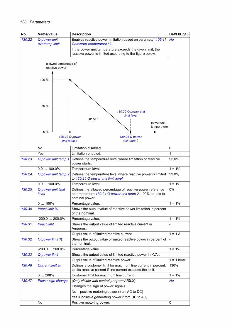
130 Parameters
130.22 Q power unit overtemp limit
Enables reactive power limitation based on parameter 105.11 Converter temperature %.
If the power unit temperature exceeds the given limit, the reactive power is limited according to the figure below.
No
No Limitation disabled. 0
Yes Limitation enabled. 1
130.23 Q power unit temp 1 Defines the temperature level where limitation of reactive power starts.
95.0%
0.0 … 100.0% Temperature level. 1 = 1%
130.24 Q power unit temp 2 Defines the temperature level where reactive power is limited to 130.25 Q power unit limit level.
99.0%
0.0 … 100.0% Temperature level. 1 = 1%
130.25 Q power unit limit level
Defines the allowed percentage of reactive power reference at temperature 130.24 Q power unit temp 2. 100% equals to nominal power.
0%
0 … 100% Percentage value. 1 = 1%
130.30 Ireact limit % Shows the output value of reactive power limitation in percent of the nominal.
-
-200.0 … 200.0% Percentage value. 1 = 1%
130.31 Ireact limit Shows the output value of limited reactive current in Amperes.
-
- Output value of limited reactive current. 1 = 1 A
130.32 Q power limit % Shows the output value of limited reactive power in percent of the nominal.
-
-200.0 … 200.0% Percentage value. 1 = 1%
130.33 Q power limit Shows the output value of limited reactive power in kVAr. -
- Output value of limited reactive power. 1 = 1 kVAr
130.46 Current limit % Defines a customer limit for maximum line current in percent. Limits reactive current if line current exceeds the limit.
130%
0 … 200% Customer limit for maximum line current. 1 = 1%
130.47 Power sign change (Only visible with control program AISLX)
Changes the sign of power signals.
No = positive motoring power (from AC to DC)
Yes = positive generating power (from DC to AC)
No
No Positive motoring power. 0
No. Name/Value Description Def/FbEq16
100 %
50 %
0 %
130.25 Q power unit limit level
power unit temperature
130.23 Q power unit temp 1
slope 1
allowed percentage of reactive power
130.24 Q power unit temp 2
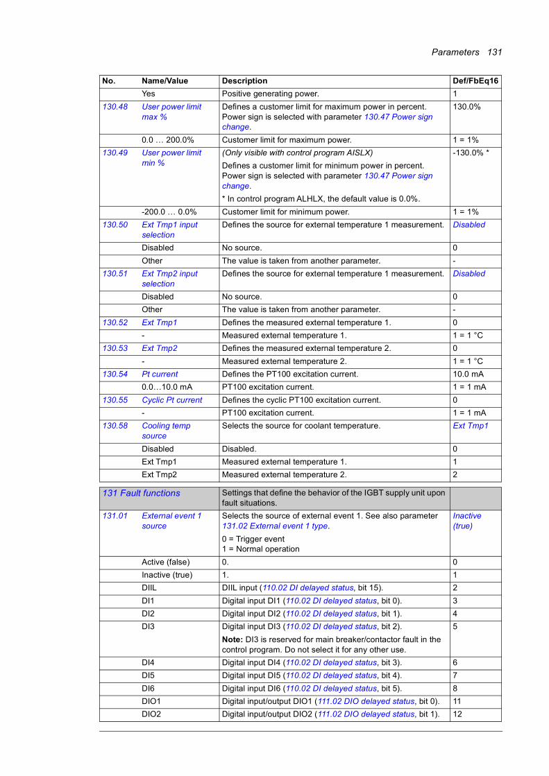
Parameters 131
Yes Positive generating power. 1
130.48 User power limit max %
Defines a customer limit for maximum power in percent. Power sign is selected with parameter 130.47 Power sign change.
130.0%
0.0 … 200.0% Customer limit for maximum power. 1 = 1%
130.49 User power limit min %
(Only visible with control program AISLX)
Defines a customer limit for minimum power in percent. Power sign is selected with parameter 130.47 Power sign change.
* In control program ALHLX, the default value is 0.0%.
-130.0% *
-200.0 … 0.0% Customer limit for minimum power. 1 = 1%
130.50 Ext Tmp1 input selection
Defines the source for external temperature 1 measurement. Disabled
Disabled No source. 0
Other The value is taken from another parameter. -
130.51 Ext Tmp2 input selection
Defines the source for external temperature 1 measurement. Disabled
Disabled No source. 0
Other The value is taken from another parameter. -
130.52 Ext Tmp1 Defines the measured external temperature 1. 0
- Measured external temperature 1. 1 = 1 °C
130.53 Ext Tmp2 Defines the measured external temperature 2. 0
- Measured external temperature 2. 1 = 1 °C
130.54 Pt current Defines the PT100 excitation current. 10.0 mA
0.0…10.0 mA PT100 excitation current. 1 = 1 mA
130.55 Cyclic Pt current Defines the cyclic PT100 excitation current. 0
- PT100 excitation current. 1 = 1 mA
130.58 Cooling temp source
Selects the source for coolant temperature. Ext Tmp1
Disabled Disabled. 0
Ext Tmp1 Measured external temperature 1. 1
Ext Tmp2 Measured external temperature 2. 2
131131 Fault functions Settings that define the behavior of the IGBT supply unit upon
fault situations.
131.01 External event 1 source
Selects the source of external event 1. See also parameter 131.02 External event 1 type.
0 = Trigger event1 = Normal operation
Inactive (true)
Active (false) 0. 0
Inactive (true) 1. 1
DIIL DIIL input (110.02 DI delayed status, bit 15). 2
DI1 Digital input DI1 (110.02 DI delayed status, bit 0). 3
DI2 Digital input DI2 (110.02 DI delayed status, bit 1). 4
DI3 Digital input DI3 (110.02 DI delayed status, bit 2).
Note: DI3 is reserved for main breaker/contactor fault in the control program. Do not select it for any other use.
5
DI4 Digital input DI4 (110.02 DI delayed status, bit 3). 6
DI5 Digital input DI5 (110.02 DI delayed status, bit 4). 7
DI6 Digital input DI6 (110.02 DI delayed status, bit 5). 8
DIO1 Digital input/output DIO1 (111.02 DIO delayed status, bit 0). 11
DIO2 Digital input/output DIO2 (111.02 DIO delayed status, bit 1). 12
No. Name/Value Description Def/FbEq16
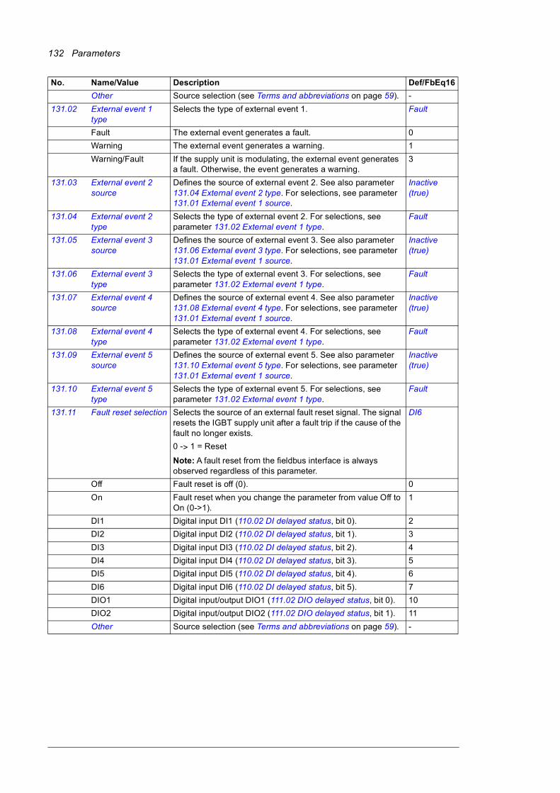
132 Parameters
Other Source selection (see Terms and abbreviations on page 59). -
131.02 External event 1 type
Selects the type of external event 1. Fault
Fault The external event generates a fault. 0
Warning The external event generates a warning. 1
Warning/Fault If the supply unit is modulating, the external event generates a fault. Otherwise, the event generates a warning.
3
131.03 External event 2 source
Defines the source of external event 2. See also parameter 131.04 External event 2 type. For selections, see parameter 131.01 External event 1 source.
Inactive (true)
131.04 External event 2 type
Selects the type of external event 2. For selections, see parameter 131.02 External event 1 type.
Fault
131.05 External event 3 source
Defines the source of external event 3. See also parameter 131.06 External event 3 type. For selections, see parameter 131.01 External event 1 source.
Inactive (true)
131.06 External event 3 type
Selects the type of external event 3. For selections, see parameter 131.02 External event 1 type.
Fault
131.07 External event 4 source
Defines the source of external event 4. See also parameter 131.08 External event 4 type. For selections, see parameter 131.01 External event 1 source.
Inactive (true)
131.08 External event 4 type
Selects the type of external event 4. For selections, see parameter 131.02 External event 1 type.
Fault
131.09 External event 5 source
Defines the source of external event 5. See also parameter 131.10 External event 5 type. For selections, see parameter 131.01 External event 1 source.
Inactive (true)
131.10 External event 5 type
Selects the type of external event 5. For selections, see parameter 131.02 External event 1 type.
Fault
131.11 Fault reset selection Selects the source of an external fault reset signal. The signal resets the IGBT supply unit after a fault trip if the cause of the fault no longer exists.
0 -> 1 = Reset
Note: A fault reset from the fieldbus interface is always observed regardless of this parameter.
DI6
Off Fault reset is off (0). 0
On Fault reset when you change the parameter from value Off to On (0->1).
1
DI1 Digital input DI1 (110.02 DI delayed status, bit 0). 2
DI2 Digital input DI2 (110.02 DI delayed status, bit 1). 3
DI3 Digital input DI3 (110.02 DI delayed status, bit 2). 4
DI4 Digital input DI4 (110.02 DI delayed status, bit 3). 5
DI5 Digital input DI5 (110.02 DI delayed status, bit 4). 6
DI6 Digital input DI6 (110.02 DI delayed status, bit 5). 7
DIO1 Digital input/output DIO1 (111.02 DIO delayed status, bit 0). 10
DIO2 Digital input/output DIO2 (111.02 DIO delayed status, bit 1). 11
Other Source selection (see Terms and abbreviations on page 59). -
No. Name/Value Description Def/FbEq16

Parameters 133
131.12 Autoreset selection Selects faults that are automatically reset. The parameter is a 16-bit word with each bit corresponding to a fault type. Whenever a bit is set to 1, the corresponding fault is automatically reset.
Note: The autoreset function is only available in external control; see section Local control vs. external control (page 18).
WARNING! The supply unit starts automatically after the autoreset if Start, Run enable and Start enable signals are on and the control program detects no
fault. Before you activate the function, make sure that no dangerous situations can occur. The function resets the supply unit automatically and continues operation after a fault. If you select an external source for the start command and it is on, the supply unit will start immediately after fault reset.
The bits of the binary number correspond to the following faults:
0000h
0000h…FFFFh Automatic reset configuration word. 1 = 1
131.13 User selectable fault Defines the fault that can be automatically reset using parameter 131.12 Autoreset selection, bit 10 User fault. Give the fault code of the selected fault. The code is given in integer.
The faults are listed in chapter Fault tracing (page 219).
0
0…65535 Fault code. 10 = 1
131.14 Number of trials Defines the number of automatic fault resets the supply unit performs within the time defined by parameter 131.15 Total trials time.
0
0…5 Number of automatic resets. -
131.15 Total trials time Defines the time for the automatic reset function. See parameter 131.14 Number of trials.
30.0 s
1.0 … 600.0 s Time for automatic resets. 10 = 1 s
131.16 Delay time Defines the time that the supply unit will wait after each fault before attempting an automatic reset. See parameter 131.12 Autoreset selection.
0.0 s
0.0 … 120.0 s Autoreset delay. 10 = 1 s
131.20 Earth fault Selects how the supply unit reacts when an earth fault or current unbalance is detected.
Fault
No No action taken. 0
Warning The supply unit generates an AE02 Earth leakage warning. 1
Fault The supply unit trips on fault 2E01 Earth leakage. 2
No. Name/Value Description Def/FbEq16
Bit Fault0 Overcurrent1 DC overvoltage2 DC undervoltage3…9 Reserved10 User fault (from source selected by parameter 131.13 User selectable fault)11 External fault 1 (from source selected by parameter 131.01 External event 1 source)12 External fault 2 (from source selected by parameter 131.03 External event 2 source)13 External fault 3 (from source selected by parameter 131.05 External event 3 source)14 External fault 4 (from source selected by parameter 131.07 External event 4 source)15 External fault 5 (from source selected by parameter 131.09 External event 5 source)
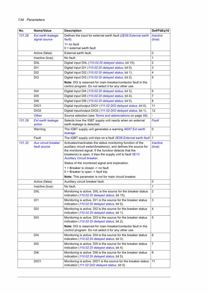
134 Parameters
131.28 Ext earth leakage signal source
Defines the input for external earth fault (2E08 External earth fault).
1= no fault0 = external earth fault
Inactive (true)
Active (false) External earth fault. 0
Inactive (true) No fault. 1
DIIL Digital input DIIL (110.02 DI delayed status, bit 15). 2
DI1 Digital input DI1 (110.02 DI delayed status, bit 0). 3
DI2 Digital input DI2 (110.02 DI delayed status, bit 1). 4
DI3 Digital input DI3 (110.02 DI delayed status, bit 2).
Note: DI3 is reserved for main breaker/contactor fault in the control program. Do not select it for any other use.
5
DI4 Digital input DI4 (110.02 DI delayed status, bit 3). 6
DI5 Digital input DI5 (110.02 DI delayed status, bit 4). 7
DI6 Digital input DI6 (110.02 DI delayed status, bit 5). 8
DIO1 Digital input/output DIO1 (111.02 DIO delayed status, bit 0). 11
DIO2 Digital input/output DIO2 (111.02 DIO delayed status, bit 1). 12
Other Source selection (see Terms and abbreviations on page 59). -
131.29 Ext earth leakage action
Selects how the IGBT supply unit reacts when an external earth leakage is detected.
Fault
Warning The IGBT supply unit generates a warning AE87 Ext earth leakage.
0
Fault The IGBT supply unit trips on a fault 2E08 External earth fault 1
131.32 Aux circuit breaker fault source
Activates/inactivates the status monitoring function of the auxiliary circuit switch/breaker(s), and defines the source for the monitored signal. If the function detects that the breaker(s) is open, it trips the supply unit to fault 5E13 Auxiliary Circuit breaker.
Status of the monitored signal and implication:
1 = Breaker is closed -> no fault0 = Breaker is open -> fault trip
Note: This parameter is not for main circuit breaker.
Inactive (true)
Active (false) Auxiliary circuit breaker fault. 0
Inactive (true) No fault. 1
DIIL Monitoring is active. DIIL is the source for the breaker status indication (110.02 DI delayed status, bit 15).
2
DI1 Monitoring is active. DI1 is the source for the breaker status indication (110.02 DI delayed status, bit 0).
3
DI2 Monitoring is active. DI2 is the source for the breaker status indication (110.02 DI delayed status, bit 1).
4
DI3 Monitoring is active. DI3 is the source for the breaker status indication (110.02 DI delayed status, bit 2).
Note: DI3 is reserved for main breaker/contactor fault in the control program. Do not select it for any other use.
5
DI4 Monitoring is active. DI4 is the source for the breaker status indication (110.02 DI delayed status, bit 3).
6
DI5 Monitoring is active. DI5 is the source for the breaker status indication (110.02 DI delayed status, bit 4).
7
DI6 Monitoring is active. DI6 is the source for the breaker status indication (110.02 DI delayed status, bit 5).
8
DIO1 Monitoring is active. DIO1 is the source for the breaker status indication (111.02 DIO delayed status, bit 0).
11
No. Name/Value Description Def/FbEq16

Parameters 135
DIO2 Monitoring is active. DIO2 is the source for the breaker status indication (111.02 DIO delayed status, bit 1).
12
Other Source selection (see Terms and abbreviations on page 59). -
131.33 Cabinet temperature fault source
Activates/inactivates the monitoring for the cabinet thermal switch, and defines the source for the monitored signal. If the monitoring detects an overtemperature, it trips the supply unit to fault 4E06 Cabinet or LCL overtemperature.
Status of the monitored signal and implication:
1 = Temperature is normal -> no fault0 = Overtemperature -> fault trip
DI1
Active (false) Monitoring function is active. 0
Inactive (true) Monitoring function is inactive. 1
DIIL Monitoring function is active and it reads the status indication through DIIL (110.02 DI delayed status, bit 15).
2
DI1 Monitoring function is active and it reads the status indication through DI1 (110.02 DI delayed status, bit 0).
3
DI2 Monitoring function is active and it reads the status indication through DI2 (110.02 DI delayed status, bit 1).
4
DI3 Monitoring function is active and it reads the status indication through DI3 (110.02 DI delayed status, bit 2).
5
DI4 Monitoring function is active and it reads the status indication through DI4 (110.02 DI delayed status, bit 3).
6
DI5 Monitoring function is active and it reads the status indication through DI5 (110.02 DI delayed status, bit 4).
7
DI6 Monitoring function is active and it reads the status indication through DI6 (110.02 DI delayed status, bit 5).
8
DIO1 Monitoring function is active and it reads the status indication through DIO1 (111.02 DIO delayed status, bit 0).
11
DIO2 Monitoring function is active and it reads the status indication through DIO2 (111.02 DIO delayed status, bit 1).
12
Other Source selection (see Terms and abbreviations on page 59). -
131.34 Cabinet temperature supervision
Selects whether there is a delay in monitoring the parameter 131.33 Cabinet temperature fault source. If this parameter is set to When modulating, the monitoring is started after the modulation has started. Otherwise there is no delay for the monitoring.
When modulating
Always There is no delay for the monitoring. 0
When modulating Cabinet temperature monitoring is started after the modulation has started.
1
131.35 Main fan fault function
Selects how the supply unit reacts when a main fan fault is detected.
Fault
Fault The supply unit trips on a fault 5E00 Fan. 0
Warning The supply unit generates a warning AE73 Fan. 1
No action No action taken. 1
131.38 Fuse trip fault source
Activates/inactivates the monitoring for the fuse trip, and defines the source for the monitored signal.
Inactive (true)
Active (false) Monitoring function is active. 0
Inactive (true) Monitoring function is inactive. 1
DIIL Monitoring function is active and it reads the status indication through DIIL (110.02 DI delayed status, bit 15).
2
DI1 Monitoring function is active and it reads the status indication through DI1 (110.02 DI delayed status, bit 0).
3
DI2 Monitoring function is active and it reads the status indication through DI2 (110.02 DI delayed status, bit 1).
4
No. Name/Value Description Def/FbEq16

136 Parameters
DI3 Monitoring function is active and it reads the status indication through DI3 (110.02 DI delayed status, bit 2).
5
DI4 Monitoring function is active and it reads the status indication through DI4 (110.02 DI delayed status, bit 3).
6
DI5 Monitoring function is active and it reads the status indication through DI5 (110.02 DI delayed status, bit 4).
7
DI6 Monitoring function is active and it reads the status indication through DI6 (110.02 DI delayed status, bit 5).
8
DIO1 Monitoring function is active and it reads the status indication through DIO1 (111.02 DIO delayed status, bit 0).
11
DIO2 Monitoring function is active and it reads the status indication through DIO2 (111.02 DIO delayed status, bit 1).
12
Other Source selection (see Terms and abbreviations on page 59). -
131.39 Brake chopper fault source
Activates/inactivates the monitoring for the brake chopper, and defines the source for the monitored signal.
Inactive (true)
Active (false) Monitoring function is active. 0
Inactive (true) Monitoring function is inactive. 1
DIIL Monitoring function is active and it reads the status indication through DIIL (110.02 DI delayed status, bit 15).
2
DI1 Monitoring function is active and it reads the status indication through DI1 (110.02 DI delayed status, bit 0).
3
DI2 Monitoring function is active and it reads the status indication through DI2 (110.02 DI delayed status, bit 1).
4
DI3 Monitoring function is active and it reads the status indication through DI3 (110.02 DI delayed status, bit 2).
5
DI4 Monitoring function is active and it reads the status indication through DI4 (110.02 DI delayed status, bit 3).
6
DI5 Monitoring function is active and it reads the status indication through DI5 (110.02 DI delayed status, bit 4).
7
DI6 Monitoring function is active and it reads the status indication through DI6 (110.02 DI delayed status, bit 5).
8
DIO1 Monitoring function is active and it reads the status indication through DIO1 (111.02 DIO delayed status, bit 0).
11
DIO2 Monitoring function is active and it reads the status indication through DIO2 (111.02 DIO delayed status, bit 1).
12
Other Source selection (see Terms and abbreviations on page 59). -
131.40 Disable warning messages
Selects warnings to be suppressed. The parameter is a 16-bit word with each bit corresponding to a warning. Whenever a bit is set to 1, the corresponding warning is suppressed.
The bits of this binary number correspond to the following warnings:
0000b
0000h…FFFFh Warning suppression word. 1 = 1
No. Name/Value Description Def/FbEq16
Bit Name0 Overvoltage1 Reserved.2 Encoder 13 Encoder 24 CU (Control unit) battery5…15 Reserved.
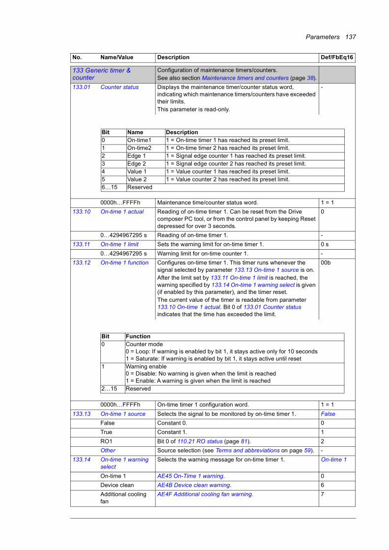
Parameters 137
133133 Generic timer & counter
Configuration of maintenance timers/counters.See also section Maintenance timers and counters (page 38).
133.01 Counter status Displays the maintenance timer/counter status word, indicating which maintenance timers/counters have exceeded their limits.This parameter is read-only.
-
0000h…FFFFh Maintenance time/counter status word. 1 = 1
133.10 On-time 1 actual Reading of on-time timer 1. Can be reset from the Drive composer PC tool, or from the control panel by keeping Reset depressed for over 3 seconds.
0
0…4294967295 s Reading of on-time timer 1. -
133.11 On-time 1 limit Sets the warning limit for on-time timer 1. 0 s
0…4294967295 s Warning limit for on-time counter 1. -
133.12 On-time 1 function Configures on-time timer 1. This timer runs whenever the signal selected by parameter 133.13 On-time 1 source is on.After the limit set by 133.11 On-time 1 limit is reached, the warning specified by 133.14 On-time 1 warning select is given (if enabled by this parameter), and the timer reset.The current value of the timer is readable from parameter 133.10 On-time 1 actual. Bit 0 of 133.01 Counter status indicates that the time has exceeded the limit.
00b
0000h…FFFFh On-time timer 1 configuration word. 1 = 1
133.13 On-time 1 source Selects the signal to be monitored by on-time timer 1. False
False Constant 0. 0
True Constant 1. 1
RO1 Bit 0 of 110.21 RO status (page 81). 2
Other Source selection (see Terms and abbreviations on page 59). -
133.14 On-time 1 warning select
Selects the warning message for on-time timer 1. On-time 1
On-time 1 AE45 On-Time 1 warning. 0
Device clean AE4B Device clean warning. 6
Additional cooling fan
AE4F Additional cooling fan warning. 7
No. Name/Value Description Def/FbEq16
Bit Name Description0 On-time1 1 = On-time timer 1 has reached its preset limit.1 On-time2 1 = On-time timer 2 has reached its preset limit.2 Edge 1 1 = Signal edge counter 1 has reached its preset limit.3 Edge 2 1 = Signal edge counter 2 has reached its preset limit.4 Value 1 1 = Value counter 1 has reached its preset limit.5 Value 2 1 = Value counter 2 has reached its preset limit.6…15 Reserved
Bit Function0 Counter mode
0 = Loop: If warning is enabled by bit 1, it stays active only for 10 seconds1 = Saturate: If warning is enabled by bit 1, it stays active until reset
1 Warning enable0 = Disable: No warning is given when the limit is reached1 = Enable: A warning is given when the limit is reached
2…15 Reserved

138 Parameters
Cabinet fan AE4D Cabinet fan warning. 8
DC-capacitor AE4C DC capacitor warning. 9
133.20 On-time 2 actual Reading of on-time timer 2. Can be reset from the Drive composer PC tool, or from the control panel by keeping Reset depressed for over 3 seconds.
-
0…4294967295 s Reading of on-time timer 2. -
133.21 On-time 2 limit Sets the warning limit for on-time timer 2. 0 s
0…4294967295 s Warning limit for on-time counter 2. -
133.22 On-time 2 function Configures on-time timer 2. This timer runs whenever the signal selected by parameter 133.23 On-time 2 source is on.After the limit set by 133.21 On-time 2 limit is reached, the warning specified by 133.24 On-time 2 warning select is given (if enabled by this parameter), and the timer reset.The current value of the timer is readable from parameter 133.20 On-time 2 actual. Bit 1 of 133.01 Counter status indicates that the time has exceeded the limit.
00b
0000h…FFFFh On-time timer 2 configuration word. 1 = 1
133.23 On-time 2 source Selects the signal to be monitored by on-time timer 2. False
False Constant 0. 0
True Constant 1. 1
RO1 Bit 0 of 110.21 RO status (page 81). 2
Other Source selection (see Terms and abbreviations on page 59). -
133.24 On-time 2 warning select
Selects the warning message for on-time timer 2. On-time 2
On-time 2 AE46 On-Time 2 warning. 1
Device clean AE4B Device clean warning. 6
Additional cool fan AE4F Additional cooling fan warning. 7
Cabinet fan AE4D Cabinet fan warning. 8
DC-capacitor AE4C DC capacitor warning. 9
133.30 Edge counter 1 actual
Reading of signal edge counter 1. Can be reset from the Drive composer PC tool, or from the control panel by keeping Reset depressed for over 3 seconds.
-
0…4294967295 Reading of signal edge counter 1. -
133.31 Edge counter 1 limit Sets the warning limit for signal edge counter 1. 0
0…4294967295 Warning limit for signal edge counter 1. -
No. Name/Value Description Def/FbEq16
Bit Function0 Counter mode
0 = Loop: If warning is enabled by bit 1, it stays active only for 10 seconds1 = Saturate: If warning is enabled by bit 1, it stays active until reset
1 Warning enable0 = Disable: No warning is given when the limit is reached1 = Enable: A warning is given when the limit is reached
2…15 Reserved

Parameters 139
133.32 Edge counter 1 func Configures signal edge counter 1. This counter is incremented every time the signal selected by parameter 133.33 Edge counter 1 source switches on or off (or either, depending on the setting of this parameter). A divisor may be applied to the count (see 133.34 Edge counter 1 divider).After the limit set by 133.31 Edge counter 1 limit is reached, the warning specified by 133.35 Edge counter 1 warning selection is given (if enabled by this parameter), and the counter reset.The current value of the counter is readable from parameter 133.30 Edge counter 1 actual. Bit 2 of 133.01 Counter status indicates that the count has exceeded the limit.
0000b
0000h…FFFFh Edge counter 1 configuration word. 1 = 1
133.33 Edge counter 1 source
Selects the signal to be monitored by signal edge counter 1. False
False Constant 0. 0
True Constant 1. 1
RO1 Bit 0 of 110.21 RO status (page 81). 2
Other Source selection (see Terms and abbreviations on page 59). -
133.34 Edge counter 1 divider
Divisor for signal edge counter 1. Determines how many signal edges increment the counter by 1.
1
1…4294967295 Divisor for signal edge counter 1. -
133.35 Edge counter 1 warning selection
Selects the warning message for signal edge counter 1. Edge counter 1
Edge counter 1 AE47 Edge counter 1 warning. 2
Main contactor AE43 Main contactor warning. 11
Output relay AE40 Output relay warning. 12
Supply unit starts AE41 Supply unit starts warning. 13
Power ups AE42 Power ups warning. 14
DC-charge AE44 DC charge warning. 15
133.40 Edge counter 2 actual
Reading of signal edge counter 2. Can be reset from the Drive composer PC tool, or from the control panel by keeping Reset depressed for over 3 seconds.
-
0…4294967295 Reading of signal edge counter 2. -
133.41 Edge counter 2 limit Sets the warning limit for signal edge counter 2. 0
0…4294967295 Warning limit for signal edge counter 2. -
No. Name/Value Description Def/FbEq16
Bit Function0 Counter mode
0 = Loop: If warning is enabled by bit 1, it stays active only for 10 seconds1 = Saturate: If warning is enabled by bit 1, it stays active until reset
1 Warning enable0 = Disable: No warning is given when the limit is reached1 = Enable: A warning is given when the limit is reached
2 Count rising edges0 = Disable: Rising edges are not counted1 = Enable: Rising edges are counted
3 Count falling edges0 = Disable: Falling edges are not counted1 = Enable: Falling edges are counted
4…15 Reserved

140 Parameters
133.42 Edge counter 2 function
Configures signal edge counter 2. This counter is incremented every time the signal selected by parameter 133.43 Edge counter 2 source switches on or off (or either, depending on the setting of this parameter). A divisor may be applied to the count (see 133.44 Edge counter 2 divider).After the limit set by 133.41 Edge counter 2 limit is reached, the warning specified by 133.45 Edge counter 2 warning selection is given (if enabled by this parameter), and the counter reset.The current value of the counter is readable from parameter 133.40 Edge counter 2 actual. Bit 3 of 133.01 Counter status indicates that the count has exceeded the limit.
0000b
0000h…FFFFh Edge counter 2 configuration word. 1 = 1
133.43 Edge counter 2 source
Selects the signal to be monitored by signal edge counter 2. False
False 0. 0
True 1. 1
RO1 Bit 0 of RO status (page 81). 2
Other Source selection (see Terms and abbreviations on page 59). -
133.44 Edge counter 2 divider
Divisor for signal edge counter 2. Determines how many signal edges increment the counter by 1.
1
1…4294967295 Divisor for signal edge counter 2. -
133.45 Edge counter 2 warning selection
Selects the warning message for signal edge counter 2. Edge counter 2
Edge counter 2 AE48 Edge counter 2 warning. 3
Main contactor AE43 Main contactor warning. 11
Output relay AE40 Output relay warning. 12
Supply unit starts AE41 Supply unit starts warning. 13
Power ups AE42 Power ups warning. 14
DC-charge AE44 DC charge warning. 15
133.50 Value counter 1 actual
Reading of value counter 1. Can be reset from the Drive composer PC tool, or from the control panel by keeping Reset depressed for over 3 seconds.
-
-2147483008 … 2147483008
Reading of value counter 1. -
133.51 Value counter 1 limit Sets the warning limit for value counter 1. 0
-2147483008 … 2147483008
Warning limit for value counter 1. -
No. Name/Value Description Def/FbEq16
Bit Function0 Counter mode
0 = Loop: If warning is enabled by bit 1, it stays active only for 10 seconds1 = Saturate: If warning is enabled by bit 1, it stays active until reset
1 Warning enable0 = Disable: No warning is given when the limit is reached1 = Enable: A warning is given when the limit is reached
2 Count rising edges0 = Disable: Rising edges are not counted1 = Enable: Rising edges are counted
3 Count falling edges0 = Disable: Falling edges are not counted1 = Enable: Falling edges are counted
4…15 Reserved
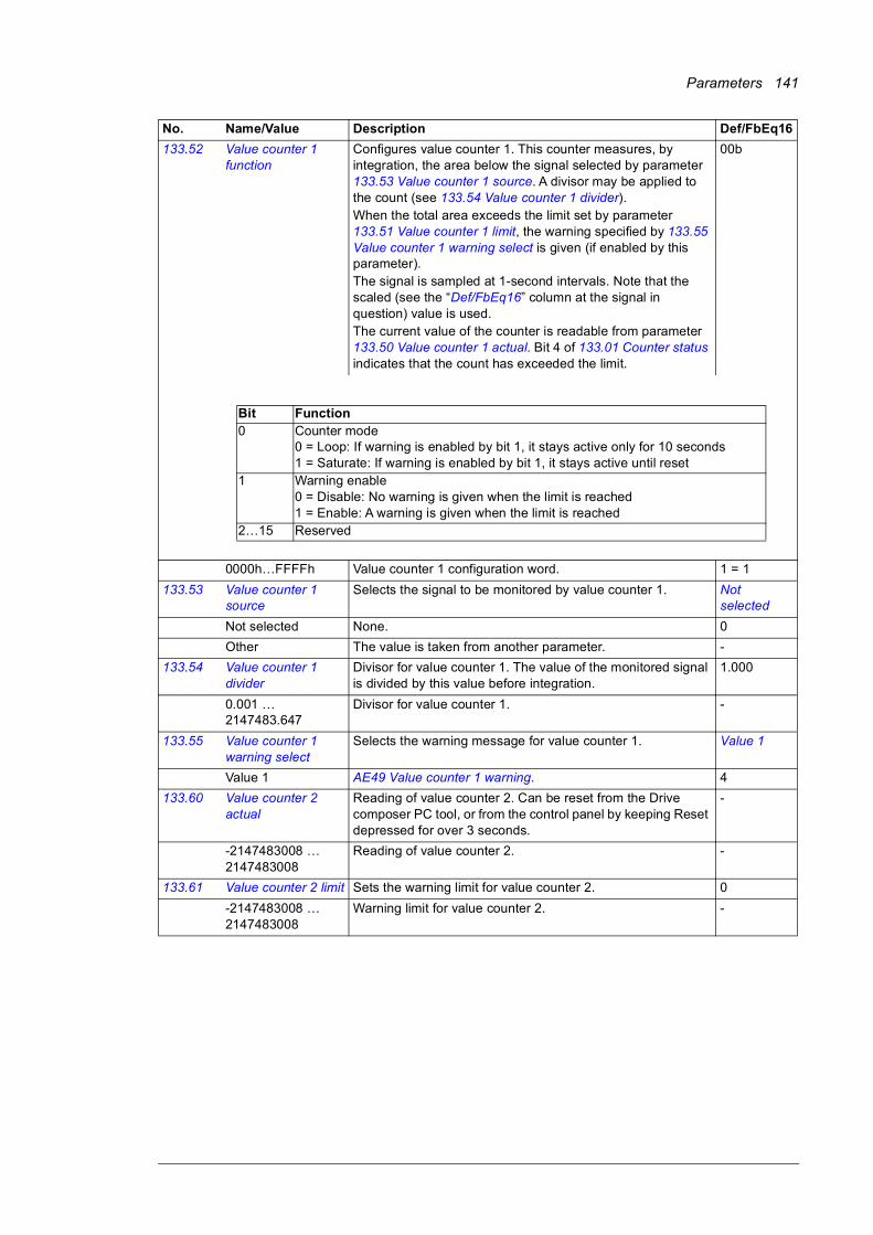
Parameters 141
133.52 Value counter 1 function
Configures value counter 1. This counter measures, by integration, the area below the signal selected by parameter 133.53 Value counter 1 source. A divisor may be applied to the count (see 133.54 Value counter 1 divider).When the total area exceeds the limit set by parameter 133.51 Value counter 1 limit, the warning specified by 133.55 Value counter 1 warning select is given (if enabled by this parameter).The signal is sampled at 1-second intervals. Note that the scaled (see the “Def/FbEq16” column at the signal in question) value is used.The current value of the counter is readable from parameter 133.50 Value counter 1 actual. Bit 4 of 133.01 Counter status indicates that the count has exceeded the limit.
00b
0000h…FFFFh Value counter 1 configuration word. 1 = 1
133.53 Value counter 1 source
Selects the signal to be monitored by value counter 1. Not selected
Not selected None. 0
Other The value is taken from another parameter. -
133.54 Value counter 1 divider
Divisor for value counter 1. The value of the monitored signal is divided by this value before integration.
1.000
0.001 … 2147483.647
Divisor for value counter 1. -
133.55 Value counter 1 warning select
Selects the warning message for value counter 1. Value 1
Value 1 AE49 Value counter 1 warning. 4
133.60 Value counter 2 actual
Reading of value counter 2. Can be reset from the Drive composer PC tool, or from the control panel by keeping Reset depressed for over 3 seconds.
-
-2147483008 … 2147483008
Reading of value counter 2. -
133.61 Value counter 2 limit Sets the warning limit for value counter 2. 0
-2147483008 … 2147483008
Warning limit for value counter 2. -
No. Name/Value Description Def/FbEq16
Bit Function0 Counter mode
0 = Loop: If warning is enabled by bit 1, it stays active only for 10 seconds1 = Saturate: If warning is enabled by bit 1, it stays active until reset
1 Warning enable0 = Disable: No warning is given when the limit is reached1 = Enable: A warning is given when the limit is reached
2…15 Reserved

142 Parameters
133.62 Value counter 2 function
Configures value counter 2. This counter measures, by integration, the area below the signal selected by parameter 133.63 Value counter 2 source. A divisor may be applied to the count (see 133.64 Value counter 2 divider).When the total area exceeds the limit set by parameter 133.61 Value counter 2 limit, the warning specified by 133.65 Value counter 2 warning selection is given (if enabled by this parameter).The signal is sampled at 1-second intervals. Note that the scaled (see the “FbEq” column at the signal in question) value is used.The current value of the counter is readable from parameter 133.60 Value counter 2 actual. Bit 5 of 133.01 Counter status indicates that the count has exceeded the limit.
00b
0000h…FFFFh Value counter 2 configuration word. 1 = 1
133.63 Value counter 2 source
Selects the signal to be monitored by value counter 2. Not selected
Not selected None. 0
Other The value is taken from another parameter. -
133.64 Value counter 2 divider
Divisor for value counter 2. The value of the monitored signal is divided by this value before integration.
1.000
0.001 … 2147483.647
Divisor for value counter 1. -
133.65 Value counter 2 warning selection
Selects the warning message for value counter 2. Value 2
Value 2 AE4A Value counter 2 warning. 5
136136 Load analyzer Peak value and amplitude logger settings.
See also section Load analyzer (page 38).
136.01 PVL signal source Selects the signal to be monitored by the peak value logger.
The signal is filtered using the filtering time specified by parameter 136.02 PVL filter time.
The peak value is stored, along with other pre-selected signals at the time, into parameters 136.10…136.15.
The peak value logger can be reset using parameter 136.09 Reset loggers. The date and time of the last reset are stored into parameters 136.16 and 136.17 respectively.
Converter current
Zero None (peak value logger disabled). 0
DC voltage 101.01 DC voltage (page 63). 1
Frequency 101.08 Frequency (page 63). 2
Grid voltage 101.09 Grid voltage (page 63). 3
Power 101.12 Power (page 63). 4
Reactive power 101.14 Reactive power (page 63). 5
Converter current 101.20 Converter current (page 64). 6
Converter current % 101.21 Converter current % (page 64). 7
No. Name/Value Description Def/FbEq16
Bit Function0 Counter mode
0 = Loop: If warning is enabled by bit 1, it stays active only for 10 seconds1 = Saturate: If warning is enabled by bit 1, it stays active until reset
1 Warning enable0 = Disable: No warning is given when the limit is reached1 = Enable: A warning is given when the limit is reached
2…15 Reserved

Parameters 143
Apparent power 101.10 Apparent power (page 63). 8
Power % 101.13 Power % (page 63). 9
Converter temperature %
105.11 Converter temperature % (page 71). 10
CosPhi 101.16 CosPhi (page 63). 11
Ambient temperature
101.70 Ambient temperature % (page 65). 14
Reactive power % 101.15 Reactive power % (page 63). 17
Other The value is taken from another parameter. -
136.02 PVL filter time Peak value logger filtering time. See parameter 136.01 PVL signal source.
2.00 s
0.00 … 120.00 s Peak value logger filtering time. 100 = 1 s
136.06 AL2 signal source Selects the signal to be monitored by amplitude logger 2. The signal is sampled at 200-millisecond intervals when the IGBT supply unit is running.
The results are displayed by parameters 136.40…136.49. Each parameter represents an amplitude range, and shows what portion of the samples fall within that range.
The signal value corresponding to 100% is defined by parameter 136.07 AL2 signal scaling.
Amplitude logger 2 can be reset using parameter 136.09 Reset loggers. The date and time of the last reset are stored into parameters 136.50 and 136.51 respectively.
For the selections, see parameter 136.01 PVL signal source.
Ambient temperature
136.07 AL2 signal scaling Defines the signal value that corresponds to 100% amplitude. 100.00
0.00 … 32767.00 Signal value corresponding to 100%. 1 = 1
136.09 Reset loggers Resets the peak value logger and/or amplitude logger 2. (Amplitude logger 1 cannot be reset.)
Done
Done Reset completed or not requested (normal operation). 0
All Reset both the peak value logger and amplitude logger 2. 1
PVL Reset the peak value logger. 2
AL2 Reset amplitude logger 2. 3
136.10 PVL peak value Peak value recorded by the peak value logger. 0.00
-32768.00 … 32767.00
Peak value. 1 = 1
136.11 PVL peak date The date on which the peak value was recorded. -
- Peak occurrence date. -
136.12 PVL peak time The time at which the peak value was recorded. -
- Peak occurrence time. -
136.13 PVL current at peak Line current at the moment the peak value was recorded. 0.00 A
-32768.00 … 32767.00 A
Line current at peak. 1 = 1 A
136.14 PVL DC voltage at peak
Voltage in the intermediate DC circuit at the moment the peak value was recorded.
0.00 V
0.00 … 2000.00 V DC voltage at peak. 10 = 1 V
136.15 PVL power at peak Power at the moment the peak value was recorded. 0.00 kW
-32768.00 … 32767.00 kW
Power at peak. 1 = 1 kW
136.16 PVL reset date The date on which the peak value logger was last reset. -
- Last reset date of the peak value logger. -
136.17 PVL reset time The time at which the peak value logger was last reset. -
- Last reset time of the peak value logger. -
No. Name/Value Description Def/FbEq16

144 Parameters
136.20 AL1 below 10% Percentage of samples recorded by amplitude logger 1 that fall between 0 and 10%.
0.00%
0.00 … 100.00% Amplitude logger 1 samples between 0 and 10%. 1 = 1%
136.21 AL1 10 to 20% Percentage of samples recorded by amplitude logger 1 that fall between 10 and 20%.
0.00%
0.00 … 100.00% Amplitude logger 1 samples between 10 and 20%. 1 = 1%
136.22 AL1 20 to 30% Percentage of samples recorded by amplitude logger 1 that fall between 20 and 30%.
0.00%
0.00 … 100.00% Amplitude logger 1 samples between 20 and 30%. 1 = 1%
136.23 AL1 30 to 40% Percentage of samples recorded by amplitude logger 1 that fall between 30 and 40%.
0.00%
0.00 … 100.00% Amplitude logger 1 samples between 30 and 40%. 1 = 1%
136.24 AL1 40 to 50% Percentage of samples recorded by amplitude logger 1 that fall between 40 and 50%.
0.00%
0.00 … 100.00% Amplitude logger 1 samples between 40 and 50%. 1 = 1%
136.25 AL1 50 to 60% Percentage of samples recorded by amplitude logger 1 that fall between 50 and 60%.
0.00%
0.00 … 100.00% Amplitude logger 1 samples between 50 and 60%. 1 = 1%
136.26 AL1 60 to 70% Percentage of samples recorded by amplitude logger 1 that fall between 60 and 70%.
0.00%
0.00 … 100.00% Amplitude logger 1 samples between 60 and 70%. 1 = 1%
136.27 AL1 70 to 80% Percentage of samples recorded by amplitude logger 1 that fall between 70 and 80%.
0.00%
0.00 … 100.00% Amplitude logger 1 samples between 70 and 80%. 1 = 1%
136.28 AL1 80 to 90% Percentage of samples recorded by amplitude logger 1 that fall between 80 and 90%.
0.00%
0.00 … 100.00% Amplitude logger 1 samples between 80 and 90%. 1 = 1%
136.29 AL1 over 90% Percentage of samples recorded by amplitude logger 1 that exceed 90%.
0.00%
0.00 … 100.00% Amplitude logger 1 samples over 90%. 1 = 1%
136.40 AL2 below 10% Percentage of samples recorded by amplitude logger 2 that fall between 0 and 10%.
0.00%
0.00 … 100.00% Amplitude logger 2 samples between 0 and 10%. 1 = 1%
136.41 AL2 10 to 20% Percentage of samples recorded by amplitude logger 2 that fall between 10 and 20%.
0.00%
0.00 … 100.00% Amplitude logger 2 samples between 10 and 20%. 1 = 1%
136.42 AL2 20 to 30% Percentage of samples recorded by amplitude logger 2 that fall between 20 and 30%.
0.00%
0.00 … 100.00% Amplitude logger 2 samples between 20 and 30%. 1 = 1%
136.43 AL2 30 to 40% Percentage of samples recorded by amplitude logger 2 that fall between 30 and 40%.
0.00%
0.00 … 100.00% Amplitude logger 2 samples between 30 and 40%. 1 = 1%
136.44 AL2 40 to 50% Percentage of samples recorded by amplitude logger 2 that fall between 40 and 50%.
0.00%
0.00 … 100.00% Amplitude logger 2 samples between 40 and 50%. 1 = 1%
136.45 AL2 50 to 60% Percentage of samples recorded by amplitude logger 2 that fall between 50 and 60%.
0.00%
0.00 … 100.00% Amplitude logger 2 samples between 50 and 60%. 1 = 1%
136.46 AL2 60 to 70% Percentage of samples recorded by amplitude logger 2 that fall between 60 and 70%.
0.00%
0.00 … 100.00% Amplitude logger 2 samples between 60 and 70%. 1 = 1%
No. Name/Value Description Def/FbEq16

Parameters 145
136.47 AL2 70 to 80% Percentage of samples recorded by amplitude logger 2 that fall between 70 and 80%.
0.00%
0.00 … 100.00% Amplitude logger 2 samples between 70 and 80%. 1 = 1%
136.48 AL2 80 to 90% Percentage of samples recorded by amplitude logger 2 that fall between 80 and 90%.
0.00%
0.00 … 100.00% Amplitude logger 2 samples between 80 and 90%. 1 = 1%
136.49 AL2 over 90% Percentage of samples recorded by amplitude logger 2 that exceed 90%.
0.00%
0.00 … 100.00% Amplitude logger 2 samples over 90%. 1 = 1%
136.50 AL2 reset date The date on which amplitude logger 2 was last reset. -
- Last reset date of amplitude logger 2. -
136.51 AL2 reset time The time at which amplitude logger 2 was last reset. -
- Last reset time of amplitude logger 2. -
146146 Monitoring settings Scaling settings.
146.01 Power scaling Defines the power and also active current and percent reference depending on parameter 122.06 Power ref type, that corresponds to 10000 for fieldbus communication with Transparent 16 profile.
Also defines the 16-bit scaling of 101.04 Active current, 101.12 Power, 122.01 User Power ref, 122.03 Power ref 1, 122.05 Power ref 2 and 122.10 Power ref.
10000.0
0.1…30000.0 Power, active current and percent reference. 1 = 1
146.02 Reactive power scaling
Defines the reactive power and also reactive current and percent reference depending on parameter 124.06 Q power ref type, that corresponds to 10000 for fieldbus communication with Transparent 16 profile.
Also defines the 16-bit scaling of 101.06 Reactive current, 101.14 Reactive power, 124.01 User Qref, 124.03 Qref 1, 124.05 Qref 2 and 124.10 Q power ref.
10000.0
0.1…30000.0 Reactive power, reactive current and percent reference. 1 = 1
146.03 Current scaling Defines the 16-bit scaling of signals 101.02 Line current and 101.20 Converter current. The value is scaled by dividing the value of this parameter by 10000.
10000 A
0…30000 A Current scaling. -
146.04 DC voltage scaling Defines the DC voltage that corresponds to 10000 for fieldbus communication with Transparent 16 profile.
Also defines the 16-bit scaling of 123.01 User DC voltage ref, 123.03 DC voltage ref 1, 123.05 DC voltage ref 2, 123.08 DC voltage ref lim and 123.11 DC voltage ref out.
100.00 V
0.10…30000.00 V DC voltage. 1 = 1 V
146.15 Filter time grid current
Defines the filter time for signals 101.02 Line current, 101.03 Line current %, 101.04 Active current, 101.05 Active current %, 101.06 Reactive current and 101.07 Reactive current %.
40 ms
20…20000 ms Filter time. 1 = 1 ms
146.16 Filter time grid voltage
Defines the filter time for signal 101.09 Grid voltage. 40 ms
20…20000 ms Filter time. 1 = 1 ms
146.17 Filter time grid power
Defines the filter time for signals 101.10 Apparent power, 101.11 Apparent power %, 101.12 Power, 101.13 Power %, 101.14 Reactive power and 101.15 Reactive power %.
40 ms
20…20000 ms Filter time. 1 = 1 ms
No. Name/Value Description Def/FbEq16

146 Parameters
147147 Data storage Parameters that can be written to and read from by using
source and target settings of other parameters.Note that there are different storage parameters for different data types.
See also section Data storage parameters (page 40).
147.01 Data storage 1 real32
Data storage parameter 1. 0.000
-2147483.000 …2147483.000
32-bit real type data. -
147.02 Data storage 2 real32
Data storage parameter 2. 0.000
-2147483.000 …2147483.000
32-bit real type data. -
147.03 Data storage 3 real32
Data storage parameter 3. 0.000
-2147483.000 …2147483.000
32-bit real type data. -
147.04 Data storage 4 real32
Data storage parameter 4. 0.000
-2147483.000 …2147483.000
32-bit real type data. -
147.05 Data storage 5 real32
Data storage parameter 5. 0.000
-2147483.000 …2147483.000
32-bit real type data. -
147.06 Data storage 6 real32
Data storage parameter 6. 0.000
-2147483.000 …2147483.000
32-bit real type data. -
147.07 Data storage 7 real32
Data storage parameter 7. 0.000
-2147483.000 …2147483.000
32-bit real type data. -
147.08 Data storage 8 real32
Data storage parameter 8. 0.000
-2147483.000 …2147483.000
32-bit real type data. -
147.11 Data storage 1 int32 Data storage parameter 9. 0
-2147483648… 2147483647
32-bit integer type data. -
147.12 Data storage 2 int32 Data storage parameter 10. 0
-2147483648… 2147483647
32-bit integer type data. -
147.13 Data storage 3 int32 Data storage parameter 11. 0
-2147483648… 2147483647
32-bit integer type data. -
147.14 Data storage 4 int32 Data storage parameter 12. 0
-2147483648… 2147483647
32-bit integer type data. -
147.15 Data storage 5 int32 Data storage parameter 13. 0
-2147483648… 2147483647
32-bit integer type data. -
No. Name/Value Description Def/FbEq16

Parameters 147
147.16 Data storage 6 int32 Data storage parameter 14. 0
-2147483648… 2147483647
32-bit integer type data. -
147.17 Data storage 7 int32 Data storage parameter 15. 0
-2147483648… 2147483647
32-bit integer type data. -
147.18 Data storage 8 int32 Data storage parameter 16. 0
-2147483648… 2147483647
32-bit integer type data. -
147.21 Data storage 1 int16 Data storage parameter 17. 0
-32768…32767 16-bit integer type data. 1 = 1
147.22 Data storage 2 int16 Data storage parameter 18. 0
-32768…32767 16-bit integer type data. 1 = 1
147.23 Data storage 3 int16 Data storage parameter 19. 0
-32768…32767 16-bit integer type data. 1 = 1
147.24 Data storage 4 int16 Data storage parameter 20. 0
-32768…32767 16-bit integer type data. 1 = 1
147.25 Data storage 5 int16 Data storage parameter 21. 0
-32768…32767 16-bit integer type data. 1 = 1
147.26 Data storage 6 int16 Data storage parameter 22. 0
-32768…32767 16-bit integer type data. 1 = 1
147.27 Data storage 7 int16 Data storage parameter 23. 0
-32768…32767 16-bit integer type data. 1 = 1
147.28 Data storage 8 int16 Data storage parameter 24. 0
-32768…32767 16-bit integer type data. 1 = 1
147.31 Data storage 1 real32 type
Defines the scaling of parameter 147.01 Data storage 1 real32 to and from 16-bit integer format. This scaling is used when the data storage parameter is the target of received 16-bit data (defined in parameter group 162 DDCS receive), or when the data storage parameter is the source of transmitted 16-bit data (defined in parameter group 161 DDCS transmit).The setting also defines the visible range of the storage parameter.
Unscaled
Unscaled Data storage only. Range: -2147483.264 … 2147473.264. 0
Transparent Scaling: 1 = 1. Range: -32768 … 32767. 1
General Scaling: 1 = 100. Range: -327.68 … 327.67. 2
147.32 Data storage 2 real32 type
Defines the 16-bit scaling of parameter 147.02 Data storage 2 real32.See parameter 147.31 Data storage 1 real32 type.
Unscaled
147.33 Data storage 3 real32 type
Defines the 16-bit scaling of parameter 147.03 Data storage 3 real32.See parameter 147.31 Data storage 1 real32 type.
Unscaled
147.34 Data storage 4 real32 type
Defines the 16-bit scaling of parameter 147.04 Data storage 4 real32.See parameter 147.31 Data storage 1 real32 type.
Unscaled
147.35 Data storage 5 real32 type
Defines the 16-bit scaling of parameter 147.05 Data storage 5 real32.See parameter 147.31 Data storage 1 real32 type.
Unscaled
147.36 Data storage 6 real32 type
Defines the 16-bit scaling of parameter 147.06 Data storage 6 real32.See parameter 147.31 Data storage 1 real32 type.
Unscaled
No. Name/Value Description Def/FbEq16

148 Parameters
147.37 Data storage 7 real32 type
Defines the 16-bit scaling of parameter 147.07 Data storage 7 real32.See parameter 147.31 Data storage 1 real32 type.
Unscaled
147.38 Data storage 8 real32 type
Defines the 16-bit scaling of parameter 147.08 Data storage 8 real32.See parameter 147.31 Data storage 1 real32 type.
Unscaled
149149 Panel port communication
Communication settings for the control panel port.
149.01 Node ID number Defines the node ID of the supply unit. All devices connected to the network must have a unique node ID.
Note: After setting this parameter, validate the change by setting the parameter 149.06 Refresh settings to Configure.
Note: For networked converters, it is advisable to reserve ID 1 for spare/replacement converters.
2
1…32 Node ID. 1 = 1
149.03 Baud rate Selects the maximum transfer rate of the link.
Note: Reliability of the communication may require lower setting, depending of the electrical characteristics of the wiring.
230.4 kbps
9.6 kbps 9.6 kbit/s. 0
38.4 kbps 38.4 kbit/s. 1
57.6 kbps 57.6 kbit/s. 2
86.4 kbps 86.4 kbit/s. 3
115.2 kbps 115.2 kbit/s. 4
230.4 kbps 230.4 kbit/s. 5
460.8 kbps 460.8 kbit/s. 6
921.6 kbps 921.6 kbit/s. 7
149.04 Communication loss time
Sets a timeout for control panel (or PC tool) communication. If a communication break lasts longer than the timeout, the action specified by parameter 149.05 Communication loss action is taken.
10.0 s
0.3…3000.0 s Panel/PC tool communication timeout. 10 = 1 s
149.05 Communication loss action
Selects how the supply unit reacts to a control panel (or PC tool) communication break.
Fault
No action No action taken. 0
Fault Supply unit trips on 7E01 Panel loss. 1
149.06 Refresh settings Applies the settings of parameters 149.01…149.05.
Note: Refreshing may cause a communication break, so reconnecting may be required.
Done
Done Refresh done or not requested. 0
Configure Refresh parameters 149.01…149.05. The value reverts automatically to Done.
1
150150 FBA General settings for fieldbus communication configuration.
150.01 FBA A enable Enables/disables communication between the IGBT supply unit and fieldbus adapter A, and specifies the slot the adapter is installed into.
Disable
Disable Communication between IGBT supply unit and fieldbus adapter A disabled.
0
Option slot 1 Communication between IGBT supply unit and fieldbus adapter A enabled. The adapter is in slot 1.
1
Option slot 2 Communication between IGBT supply unit and fieldbus adapter A enabled. The adapter is in slot 2.
2
No. Name/Value Description Def/FbEq16

Parameters 149
Option slot 3 Communication between IGBT supply unit and fieldbus adapter A enabled. The adapter is in slot 3.
3
150.02 FBA A comm loss func
Selects how the IGBT supply unit reacts upon a fieldbus communication loss. The time delay is defined by parameter 150.03 FBA A comm loss t out.
No action
No action No action taken. 0
Fault Communication loss detection active. Upon a communication loss, the IGBT supply unit trips on a 7E0B FBA A communication fault and stops.
1
Fault always IGBT supply unit trips on 7E0B FBA A communication. This occurs even though no control is expected from the fieldbus.
2
Warning IGBT supply unit generates an AE30 FBA A communication warning. This occurs even though no control is expected from the fieldbus.
WARNING! Make sure that it is safe to continue operation in case of a communication break.
3
150.03 FBA A comm loss t out
Defines the time delay before the action defined by parameter 150.02 FBA A comm loss func is taken. Time count starts when the communication link fails to update the message.
0.3 s
0.3 … 6553.5 s Time delay. 10 = 1 s
150.04 FBA A ref1 type Selects the type and scaling of reference 1 received from fieldbus adapter A.
Auto
Auto Type and scaling is chosen automatically according to the currently active operation mode.
0
Transparent No scaling is applied. 1
General Generic reference without a specific unit. 2
Frequency Reserved. 5
DC voltage The scaling is defined by parameter 146.04 DC voltage scaling.
8
Active power The scaling is defined by parameter 146.01 Power scaling. 9
Reactive power The scaling is defined by parameter 146.02 Reactive power scaling.
10
AC Voltage Reserved. 13
150.05 FBA A ref2 type Selects the type and scaling of reference 2 received from fieldbus adapter A.
For the selections, see parameter 150.04 FBA A ref1 type.
Auto
150.07 FBA A actual1 type Selects the type and scaling of actual value 1 transmitted to the fieldbus network through fieldbus adapter A.
For the selections, see parameter 150.04 FBA A ref1 type.
Auto
150.08 FBA A actual2 type Selects the type and scaling of actual value 2 transmitted to the fieldbus network through fieldbus adapter A.
For the selections, see parameter 150.04 FBA A ref1 type.
Auto
150.10 FBA A act1 transparent source
Selects the type of actual value 1 transmitted to the fieldbus network through fieldbus adapter A.
Not selected
Not selected No source selected. -
Other The value is taken from another parameter. -
150.11 FBA A act2 transparent source
Selects the type of actual value 2 transmitted to the fieldbus network through fieldbus adapter A.
Not selected
Not selected No source selected. -
Other The value is taken from another parameter. -
No. Name/Value Description Def/FbEq16

150 Parameters
150.12 FBA A debug mode Enables the display of raw (unmodified) data received from and sent to fieldbus adapter A in parameters 150.13…150.18.
Note that the changes made take effect only after reboot or setting the parameter 151.27 FBA A par refresh to Configure.
This functionality should only be used for debugging.
Disable
Disable Display of raw data from fieldbus adapter A disabled. 0
Fast Debug mode is enabled. Cyclical data update is as fast as possible which increases the CPU load on the IGBT supply unit.
1
150.13 FBA A control word Displays the control word sent by the master (PLC) to fieldbus adapter A. For details of the contents, see page 256.
This parameter is read-only.
-
0000h…FFFFh Control word sent by master to fieldbus adapter A. -
150.14 FBA A reference 1 Displays raw reference REF1 sent by the master (PLC) to fieldbus adapter A.
This parameter is read-only.
-
-2147483648… 2147483647
Raw REF1 sent by master to fieldbus adapter A.
150.15 FBA A reference 2 Displays raw reference REF2 sent by the master (PLC) to fieldbus adapter A.
This parameter is read-only.
-
-2147483648… 2147483647
Raw REF2 sent by master to fieldbus adapter A. -
150.16 FBA A status word Displays the status word sent by fieldbus adapter A to the master (PLC). For details of the contents, see page 257.
This parameter is read-only.
-
0000h…FFFFh Status word sent by fieldbus adapter A to master. -
150.17 FBA A actual value 1
Displays raw actual value ACT1 sent by fieldbus adapter A to the master (PLC).
This parameter is read-only.
-
-2147483648… 2147483647
Raw ACT1 sent by fieldbus adapter A to master. -
150.18 FBA A actual value 2
Displays raw actual value ACT2 sent by fieldbus adapter A to the master (PLC).
This parameter is read-only.
-
-2147483648… 2147483647
Raw ACT2 sent by fieldbus adapter A to master. -
150.21 FBA A timelevel sel Selects the communication speed.
In general, lower speeds reduce CPU load. The table below shows the read/write intervals for cyclic and acyclic data with each parameter setting.
*Cyclic data consists of fieldbus Control and Status words, Ref1, Ref2, Act1 and Act2.
**Acyclic data consists of the parameter data mapped to parameter groups 152 FBA A data in and 153 FBA A data out.
Normal
Normal Normal speed. 0
Fast Fast speed. 1
No. Name/Value Description Def/FbEq16
Selection Cyclic* Acyclic**Monitoring 10 ms 10 msNormal 2 ms 10 msFast 500 µs 2 msVery fast 250 µs 500 µs

Parameters 151
Very fast Very fast speed. 2
Monitoring Low speed. Optimized for PC tool communication and monitoring usage.
3
150.31 FBA B enable Enables/disables communication between the IGBT supply unit and fieldbus adapter B, and specifies the slot the adapter is installed into.
Disable
Disable Communication between IGBT supply unit and fieldbus adapter B disabled.
0
Option slot 1 Communication between IGBT supply unit and fieldbus adapter B enabled. The adapter is in slot 1.
1
Option slot 2 Communication between IGBT supply unit and fieldbus adapter B enabled. The adapter is in slot 2.
2
Option slot 3 Communication between IGBT supply unit and fieldbus adapter B enabled. The adapter is in slot 3.
3
150.32 FBA B comm loss func
Selects how the IGBT supply unit reacts upon a fieldbus communication break. The time delay is defined by parameter 150.33 FBA B comm loss timeout.
No action
No action No action taken. 0
Fault Communication loss detection active. Upon a communication loss, the IGBT supply unit trips on a 7E0C FBA B communication fault and stops.
1
Fault always IGBT supply unit trips on 7E0C FBA B communication. This occurs even though no control is expected from the fieldbus.
2
Warning IGBT supply unit generates an AE31 FBA B communication warning. This occurs even though no control is expected from the fieldbus.
WARNING! Make sure that it is safe to continue operation in case of a communication break.
3
150.33 FBA B comm loss timeout
Defines the time delay before the action defined by parameter 150.32 FBA B comm loss func is taken. Time count starts when the communication link fails to update the message.
0.3 s
0.3 … 6553.5 s Time delay. 10 = 1 s
150.34 FBA B ref1 type Selects the type and scaling of reference 1 received from fieldbus adapter B.
For the selections, see parameter 150.04 FBA A ref1 type.
Auto
150.35 FBA B ref2 type Selects the type and scaling of reference 2 received from fieldbus adapter B.
For the selections, see parameter 150.05 FBA A ref2 type.
Auto
150.36 FBA B SW sel Selects the source of the Status word to be sent to the fieldbus network through fieldbus adapter B.
Auto
Auto Source of the Status word is chosen automatically. 0
Transparent mode The source selected by parameter 150.39 FBA B SW transparent source is transmitted as the Status word to the fieldbus network through fieldbus adapter B.
1
150.37 FBA B actual 1 type Selects the type and scaling of actual value 1 transmitted to the fieldbus network through fieldbus adapter B.
For the selections, see parameter 150.07 FBA A actual1 type.
Auto
150.38 FBA B actual 2 type Selects the type and scaling of actual value 2 transmitted to the fieldbus network through fieldbus adapter B.
For the selections, see parameter 150.08 FBA A actual2 type.
Auto
150.39 FBA B SW transparent source
Selects the source of the fieldbus status word when parameter 150.36 FBA B SW sel is set to Transparent mode.
Not selected
Not selected No source selected. -
Other The value is taken from another parameter. -
No. Name/Value Description Def/FbEq16

152 Parameters
150.40 FBA B act1 transparent source
When parameter 150.37 FBA B actual 1 type is set to Transparent mode, this parameter selects the type of actual value 1 transmitted to the fieldbus network through fieldbus adapter B.
Not selected
Not selected No source selected. -
Other The value is taken from another parameter. -
150.41 FBA B act2 transparent source
Selects the type of actual value 2 transmitted to the fieldbus network through fieldbus adapter B.
Not selected
Not selected No source selected. -
Other The value is taken from another parameter. -
150.42 FBA B debug mode Enables the display of raw (unmodified) data received from and sent to fieldbus adapter B in parameters 150.43…150.48.
Note that the changes made take effect only after reboot or setting the parameter 154.27 FBA B par refresh to Configure.
This functionality should only be used for debugging.
Disable
Disable Display of raw data from fieldbus adapter B disabled. 0
Fast Debug mode is enabled. Cyclical data update is as fast as possible which increases the CPU load on the IGBT supply unit.
1
150.43 FBA B control word Displays the raw (unmodified) control word sent by the master (PLC) to fieldbus adapter B if debugging is enabled by parameter 150.42 FBA B debug mode.
This parameter is read-only.
-
00000000h … FFFFFFFFh
Control word sent by master to fieldbus adapter B. -
150.44 FBA B reference 1 Displays the raw (unmodified) reference REF1 sent by the master (PLC) to fieldbus adapter B if debugging is enabled by parameter 150.42 FBA B debug mode.
This parameter is read-only.
-
-2147483648… 2147483647
Raw REF1 sent by master to fieldbus adapter B. -
150.45 FBA B reference 2 Displays the raw (unmodified) reference REF2 sent by the master (PLC) to fieldbus adapter B if debugging is enabled by parameter 150.42 FBA B debug mode.
This parameter is read-only.
-
-2147483648… 2147483647
Raw REF2 sent by master to fieldbus adapter B. -
150.46 FBA B status word Displays the raw (unmodified) status word sent by fieldbus adapter B to the master (PLC) if debugging is enabled by parameter 150.42 FBA B debug mode.
This parameter is read-only.
-
00000000h … FFFFFFFFh
Status word sent by fieldbus adapter B to master. -
150.47 FBA B actual value 1
Displays the raw (unmodified) actual value ACT1 sent by fieldbus adapter B to the master (PLC) if debugging is enabled by parameter 150.42 FBA B debug mode.
This parameter is read-only.
-
-2147483648 … 2147483647
Raw ACT1 sent by fieldbus adapter B to master. -
No. Name/Value Description Def/FbEq16

Parameters 153
150.48 FBA B actual value 2
Displays the raw (unmodified) actual value ACT2 sent by fieldbus adapter B to the master (PLC) if debugging is enabled by parameter 150.42 FBA B debug mode.
This parameter is read-only.
-
-2147483648 … 2147483647
Raw ACT2 sent by fieldbus adapter B to master. -
150.51 FBA B timelevel sel Selects the communication speed.
In general, lower speeds reduce CPU load. The table below shows the read/write intervals for cyclic and acyclic data with each parameter setting.
*Cyclic data consists of fieldbus Control and Status words, Ref1, Ref2, Act1 and Act2.
**Acyclic data consists of the parameter data mapped to parameter groups 155 FBA B data in and 156 FBA B data out.
Normal
Normal Normal speed. 0
Fast Fast speed. 1
Very fast Very fast speed. 2
Monitoring Low speed. Optimized for PC tool communication and monitoring usage.
3
151151 FBA A settings Fieldbus adapter A configuration.
151.01 FBA A type Displays the type of the connected fieldbus adapter module.
0 = Module is not found or is not properly connected, or is disabled by parameter 150.01 FBA A enable; 1 = FPBA; 32 = FCAN; 37 = FDNA; 101 = FCNA; 128 = FENA-11/21; 132 = FPNO; 135 = FECA; 136 = FEPL; 485 = FSCA; 502 = FMBT; 2222 = FEIP; 62944 = FSEA.
Note: All types of the fieldbus adapter modules are not necessarily supported yet.
This parameter is read-only.
-
151.02 FBA A Par2 Parameters 151.02…151.26 are adapter module-specific. For more information, see the documentation of the fieldbus adapter module. Note that not all of these parameters are necessarily in use.
Note: In supply units only Trans16 profile is in use.
-
… … … …
151.26 FBA A Par26 See parameter 151.02 FBA A Par2. -
151.27 FBA A par refresh Validates any changed fieldbus adapter module configuration settings. After refreshing, the value reverts automatically to Done.
Note: This parameter cannot be changed while the IGBT supply unit is running.
Done
Done Refreshing done. 0
Configure Refreshing. 1
No. Name/Value Description Def/FbEq16
Selection Cyclic* Acyclic**Monitoring 10 ms 10 msNormal 2 ms 10 msFast 500 µs 2 msVery fast 250 µs 500 µs

154 Parameters
151.28 FBA A par table ver Displays the parameter table revision of the fieldbus adapter module mapping file stored in the memory of the IGBT supply unit.
In format axyz, where a = major revision number; xy = minor revision number; z = correction number.
This parameter is read-only.
-
Parameter table revision of adapter module. 1 = 1
151.29 FBA A drive type code
Displays the IGBT supply unit type code of the fieldbus adapter module mapping file stored in the memory of the IGBT supply unit.
This parameter is read-only.
-
0…65535 IGBT supply unit type code of fieldbus adapter module mapping file.
1 = 1
151.30 FBA A mapping file ver
Displays the fieldbus adapter module mapping file revision stored in the memory of the IGBT supply unit in decimal format.
Example: Integer 263 -> 0x107 = revision 1.07
This parameter is read-only.
-
0…65535 Mapping file revision. 1 = 1
151.31 D2FBA A comm status
Displays the status of the fieldbus adapter module communication.
-
Idle Adapter is not configured. 0
Exec.init Adapter is initializing. 1
Time out A timeout has occurred in the communication between the adapter and the IGBT supply unit.
2
Conf.err Adapter configuration error: the major or minor revision code of the common program revision in the fieldbus adapter module is not the revision required by the module (see parameter 151.32 FBA A comm SW ver), or mapping file upload has failed more than three times. Check also parameter 150.03 FBA A comm loss t out.
3
Off-line Adapter is off-line. 4
On-line Adapter is on-line. 5
Reset Adapter is performing a hardware reset. 6
151.32 FBA A comm SW ver
Displays the common program revision of the adapter module in format axyz, where a = major revision number, xy = minor revision number, z = correction number.
Example: 190A = revision 1.90A.
Common program revision of adapter module. -
151.33 FBA A appl SW ver Displays the application program revision of the adapter module in format axyz, where a = major revision number, xy = minor revision number, z = correction number or letter.
Example: 190A = revision 1.90A.
Application program version of adapter module. -
152152 FBA A data in Selection of data to be transferred from IGBT supply unit to
fieldbus controller through fieldbus adapter A.Note: 32-bit values require two consecutive parameters. Whenever a 32-bit value is selected in a data parameter, the next parameter is automatically reserved.
152.01 FBA A data in1 Parameters 152.01… select data to be transferred from the IGBT supply unit to the fieldbus controller through fieldbus adapter A.
None
None None. 0
CW 16bit Control Word (16 bits) 1
No. Name/Value Description Def/FbEq16

Parameters 155
Ref1 16bit Reference 1 (16 bits) 2
Ref2 16bit Reference 2 (16 bits) 3
SW 16bit Status Word (16 bits) 4
Act1 16bit Actual value Act1 (16 bits) 5
Act2 16bit Actual value Act2 (16 bits) 6
CW 32bit Control Word (32 bits) 11
Ref1 32bit Reference 1 (32 bits) 12
Ref2 32bit Reference 2 (32 bits) 13
SW 32bit Status Word (32 bits) 14
Act1 32bit Actual value ACT1 (32 bits) 15
Act2 32bit Actual value ACT2 (32 bits) 16
SW2 16bit Status Word 2 (16 bits) 24
… … …
152.12 FBA A data in12 See parameter 152.01 FBA A data in1. None
153153 FBA A data out Selection of data to be transferred from fieldbus controller to
IGBT supply unit through fieldbus adapter A.Note: 32-bit values require two consecutive parameters. Whenever a 32-bit value is selected in a data parameter, the next parameter is automatically reserved.
153.01 FBA data out1 Parameters 153.01… select data to be transferred from the fieldbus controller to the IGBT supply unit through fieldbus adapter A. Transfer speed can be set with parameter 150.21 FBA A timelevel sel.
None
None None. 0
CW 16bit Control Word (16 bits) 1
Ref1 16bit Reference Ref1 (16 bits) 2
Ref2 16bit Reference Ref2 (16 bits) 3
CW 32bit Control Word (32 bits) 11
Ref1 32bit Reference Ref1 (32 bits) 12
Ref2 32bit Reference Ref2 (32 bits) 13
CW2 16bit Control Word 2 (16 bits) 21
… … … …
153.12 FBA data out12 See parameter 153.01 FBA data out1. None
154154 FBA B settings Fieldbus adapter B configuration.
154.01 FBA B type Displays the type of the connected fieldbus adapter module.
0 = Module is not found or is not properly connected, or is disabled by parameter 150.31 FBA B enable; 1 = FPBA; 32 = FCAN; 37 = FDNA; 101 = FCNA; 128 = FENA-11/21; 132 = PROFINET IO; 135 = FECA; 136 = FEPL; 485 = FSCA; 62944 = FSEA.
-
154.02 FBA B Par2 Parameters 154.02…154.26 are adapter module-specific. For more information, see the documentation of the fieldbus adapter module. Note that not all of these parameters are necessarily in use.
-
… … … …
154.26 FBA B Par26 See parameter 154.02 FBA B Par2. -
No. Name/Value Description Def/FbEq16
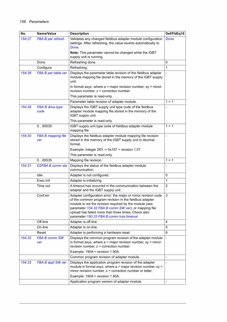
156 Parameters
154.27 FBA B par refresh Validates any changed fieldbus adapter module configuration settings. After refreshing, the value reverts automatically to Done.
Note: This parameter cannot be changed while the IGBT supply unit is running.
Done
Done Refreshing done. 0
Configure Refreshing. 1
154.28 FBA B par table ver Displays the parameter table revision of the fieldbus adapter module mapping file stored in the memory of the IGBT supply unit.
In format axyz, where a = major revision number; xy = minor revision number; z = correction number.
This parameter is read-only.
-
Parameter table revision of adapter module. 1 = 1
154.29 FBA B drive type code
Displays the IGBT supply unit type code of the fieldbus adapter module mapping file stored in the memory of the IGBT supply unit.
This parameter is read-only.
-
0…65535 IGBT supply unit type code of fieldbus adapter module mapping file.
1 = 1
154.30 FBA B mapping file ver
Displays the fieldbus adapter module mapping file revision stored in the memory of the IGBT supply unit in decimal format.
Example: Integer 263 -> 0x107 = revision 1.07
This parameter is read-only.
-
0…65535 Mapping file revision. 1 = 1
154.31 D2FBA B comm sta Displays the status of the fieldbus adapter module communication.
-
Idle Adapter is not configured. 0
Exec.init Adapter is initializing. 1
Time out A timeout has occurred in the communication between the adapter and the IGBT supply unit.
2
Conf.err Adapter configuration error: the major or minor revision code of the common program revision in the fieldbus adapter module is not the revision required by the module (see parameter 154.32 FBA B comm SW ver), or mapping file upload has failed more than three times. Check also parameter 150.33 FBA B comm loss timeout.
3
Off-line Adapter is off-line. 4
On-line Adapter is on-line. 5
Reset Adapter is performing a hardware reset. 6
154.32 FBA B comm SW ver
Displays the common program revision of the adapter module in format axyz, where a = major revision number, xy = minor revision number, z = correction number.
Example: 190A = revision 1.90A.
-
Common program revision of adapter module. -
154.33 FBA B appl SW ver Displays the application program revision of the adapter module in format axyz, where a = major revision number, xy = minor revision number, z = correction number or letter.
Example: 190A = revision 1.90A.
-
Application program version of adapter module. -
No. Name/Value Description Def/FbEq16
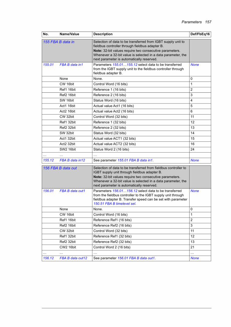
Parameters 157
155155 FBA B data in Selection of data to be transferred from IGBT supply unit to
fieldbus controller through fieldbus adapter B.Note: 32-bit values require two consecutive parameters. Whenever a 32-bit value is selected in a data parameter, the next parameter is automatically reserved.
155.01 FBA B data in1 Parameters 155.01…155.12 select data to be transferred from the IGBT supply unit to the fieldbus controller through fieldbus adapter B.
None
None None. 0
CW 16bit Control Word (16 bits) 1
Ref1 16bit Reference 1 (16 bits) 2
Ref2 16bit Reference 2 (16 bits) 3
SW 16bit Status Word (16 bits) 4
Act1 16bit Actual value Act1 (16 bits) 5
Act2 16bit Actual value Act2 (16 bits) 6
CW 32bit Control Word (32 bits) 11
Ref1 32bit Reference 1 (32 bits) 12
Ref2 32bit Reference 2 (32 bits) 13
SW 32bit Status Word (32 bits) 14
Act1 32bit Actual value ACT1 (32 bits) 15
Act2 32bit Actual value ACT2 (32 bits) 16
SW2 16bit Status Word 2 (16 bits) 24
… … …
155.12 FBA B data in12 See parameter 155.01 FBA B data in1. None
156156 FBA B data out Selection of data to be transferred from fieldbus controller to
IGBT supply unit through fieldbus adapter B.Note: 32-bit values require two consecutive parameters. Whenever a 32-bit value is selected in a data parameter, the next parameter is automatically reserved.
156.01 FBA B data out1 Parameters 156.01…156.12 select data to be transferred from the fieldbus controller to the IGBT supply unit through fieldbus adapter B. Transfer speed can be set with parameter 150.51 FBA B timelevel sel.
None
None None. 0
CW 16bit Control Word (16 bits) 1
Ref1 16bit Reference Ref1 (16 bits) 2
Ref2 16bit Reference Ref2 (16 bits) 3
CW 32bit Control Word (32 bits) 11
Ref1 32bit Reference Ref1 (32 bits) 12
Ref2 32bit Reference Ref2 (32 bits) 13
CW2 16bit Control Word 2 (16 bits) 21
… … … …
156.12 FBA B data out12 See parameter 156.01 FBA B data out1. None
No. Name/Value Description Def/FbEq16

158 Parameters
160160 DDCS communication DDCS communication configuration.
Fiber optic links connected to DDCS channels can be used to
• connect units together to build a master/follower network
• connect the converter to an external controller such as the AC500 PLC.
See also section DDCS communication with inverter unit on page 43.
160.01 M/F communication port
Selects the connection used by the master/follower functionality.
No connect
No connect None (communication disabled). 0
Slot 1A Channel A on FDCO module in slot 1 (with ZCU control unit only).
1
Slot 2A Channel A on FDCO module in slot 2 (with ZCU control unit only).
2
Slot 3A Channel A on FDCO module in slot 3 (with ZCU control unit only).
3
Slot 1B Channel B on FDCO module in slot 1 (with ZCU control unit only).
4
Slot 2B Channel B on FDCO module in slot 2 (with ZCU control unit only).
5
Slot 3B Channel B on FDCO module in slot 3 (with ZCU control unit only).
6
RDCO CH 2 Channel 2 on RDCO module (with BCU control unit only). 12
XD2D Connector XD2D.Note: This connection cannot co-exist, and is not to be confused with, drive-to-drive (D2D) communication implemented by application programming (detailed in Drive application programming manual (IEC 61131-3), 3AUA0000127808 [English]).
7
160.02 M/F node address Selects the node address for master/follower communication. No two nodes on-line may have the same address.Note: The allowable addresses for the master are 0 and 1. The allowable addresses for followers are 2…60.
1
1…254 Node address.
160.03 M/F mode Defines the role of the supply unit on the master/follower or drive-to-drive link.
Not in use
Not in use Master/follower functionality not active. 0
DDCS master The supply unit is the master on the master/follower (DDCS) link.
1
DDCS follower The supply unit is a follower on the master/follower (DDCS) link.
2
160.05 M/F HW connection Selects the topology of the master/follower link.Note: Use the setting Star if using the master/follower functionality through the XD2D connector (as opposed to a fiber optic link).
Ring
Ring The devices are connected in a ring topology. Forwarding of messages is enabled.
0
Star The devices are connected in a star topology (for example, through a branching unit). Forwarding of messages is disabled.
1
No. Name/Value Description Def/FbEq16
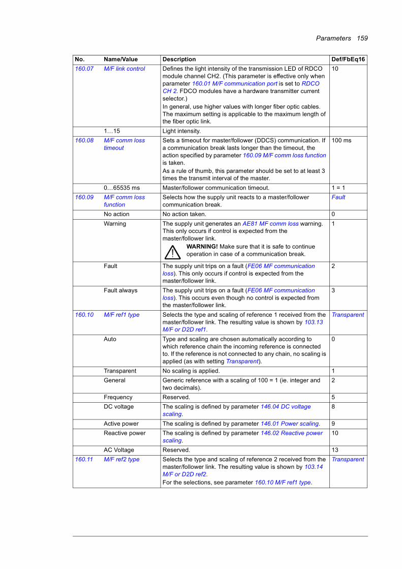
Parameters 159
160.07 M/F link control Defines the light intensity of the transmission LED of RDCO module channel CH2. (This parameter is effective only when parameter 160.01 M/F communication port is set to RDCO CH 2. FDCO modules have a hardware transmitter current selector.)In general, use higher values with longer fiber optic cables. The maximum setting is applicable to the maximum length of the fiber optic link.
10
1…15 Light intensity.
160.08 M/F comm loss timeout
Sets a timeout for master/follower (DDCS) communication. If a communication break lasts longer than the timeout, the action specified by parameter 160.09 M/F comm loss function is taken.As a rule of thumb, this parameter should be set to at least 3 times the transmit interval of the master.
100 ms
0…65535 ms Master/follower communication timeout. 1 = 1
160.09 M/F comm loss function
Selects how the supply unit reacts to a master/follower communication break.
Fault
No action No action taken. 0
Warning The supply unit generates an AE81 MF comm loss warning. This only occurs if control is expected from the master/follower link.
WARNING! Make sure that it is safe to continue operation in case of a communication break.
1
Fault The supply unit trips on a fault (FE06 MF communication loss). This only occurs if control is expected from the master/follower link.
2
Fault always The supply unit trips on a fault (FE06 MF communication loss). This occurs even though no control is expected from the master/follower link.
3
160.10 M/F ref1 type Selects the type and scaling of reference 1 received from the master/follower link. The resulting value is shown by 103.13 M/F or D2D ref1.
Transparent
Auto Type and scaling are chosen automatically according to which reference chain the incoming reference is connected to. If the reference is not connected to any chain, no scaling is applied (as with setting Transparent).
0
Transparent No scaling is applied. 1
General Generic reference with a scaling of 100 = 1 (ie. integer and two decimals).
2
Frequency Reserved. 5
DC voltage The scaling is defined by parameter 146.04 DC voltage scaling.
8
Active power The scaling is defined by parameter 146.01 Power scaling. 9
Reactive power The scaling is defined by parameter 146.02 Reactive power scaling.
10
AC Voltage Reserved. 13
160.11 M/F ref2 type Selects the type and scaling of reference 2 received from the master/follower link. The resulting value is shown by 103.14 M/F or D2D ref2.For the selections, see parameter 160.10 M/F ref1 type.
Transparent
No. Name/Value Description Def/FbEq16
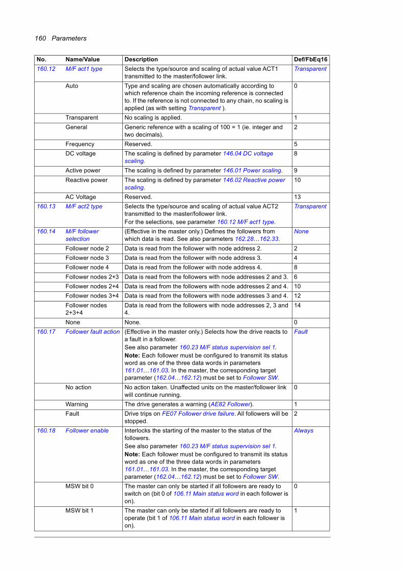
160 Parameters
160.12 M/F act1 type Selects the type/source and scaling of actual value ACT1 transmitted to the master/follower link.
Transparent
Auto Type and scaling are chosen automatically according to which reference chain the incoming reference is connected to. If the reference is not connected to any chain, no scaling is applied (as with setting Transparent ).
0
Transparent No scaling is applied. 1
General Generic reference with a scaling of 100 = 1 (ie. integer and two decimals).
2
Frequency Reserved. 5
DC voltage The scaling is defined by parameter 146.04 DC voltage scaling.
8
Active power The scaling is defined by parameter 146.01 Power scaling. 9
Reactive power The scaling is defined by parameter 146.02 Reactive power scaling.
10
AC Voltage Reserved. 13
160.13 M/F act2 type Selects the type/source and scaling of actual value ACT2 transmitted to the master/follower link.For the selections, see parameter 160.12 M/F act1 type.
Transparent
160.14 M/F follower selection
(Effective in the master only.) Defines the followers from which data is read. See also parameters 162.28…162.33.
None
Follower node 2 Data is read from the follower with node address 2. 2
Follower node 3 Data is read from the follower with node address 3. 4
Follower node 4 Data is read from the follower with node address 4. 8
Follower nodes 2+3 Data is read from the followers with node addresses 2 and 3. 6
Follower nodes 2+4 Data is read from the followers with node addresses 2 and 4. 10
Follower nodes 3+4 Data is read from the followers with node addresses 3 and 4. 12
Follower nodes 2+3+4
Data is read from the followers with node addresses 2, 3 and 4.
14
None None. 0
160.17 Follower fault action (Effective in the master only.) Selects how the drive reacts to a fault in a follower.See also parameter 160.23 M/F status supervision sel 1.Note: Each follower must be configured to transmit its status word as one of the three data words in parameters 161.01…161.03. In the master, the corresponding target parameter (162.04…162.12) must be set to Follower SW.
Fault
No action No action taken. Unaffected units on the master/follower link will continue running.
0
Warning The drive generates a warning (AE82 Follower). 1
Fault Drive trips on FE07 Follower drive failure. All followers will be stopped.
2
160.18 Follower enable Interlocks the starting of the master to the status of the followers.See also parameter 160.23 M/F status supervision sel 1.Note: Each follower must be configured to transmit its status word as one of the three data words in parameters 161.01…161.03. In the master, the corresponding target parameter (162.04…162.12) must be set to Follower SW.
Always
MSW bit 0 The master can only be started if all followers are ready to switch on (bit 0 of 106.11 Main status word in each follower is on).
0
MSW bit 1 The master can only be started if all followers are ready to operate (bit 1 of 106.11 Main status word in each follower is on).
1
No. Name/Value Description Def/FbEq16

Parameters 161
MSW bits 0 + 1 The master can only be started if all followers are ready to switch on and ready to operate (bits 0 and 1 of 106.11 Main status word in each follower are on).
2
Always The starting of the master is not interlocked to the status of the followers.
3
MSW bit 12 The master can only be started if user-definable bit 12 of 106.11 Main status word in each follower is on. See parameter 106.31 MSW bit 12 sel.
4
MSW bits 0 + 12 The master can only be started if both bit 0 and bit 12 of 106.11 Main status word in each follower are on.
5
MSW bits 1 + 12 The master can only be started if both bit 1 and bit 12 of 106.11 Main status word in each follower are on.
6
160.23 M/F status supervision sel 1
(This parameter is only effective when the supply unit is the master on a D2D link. See parameters 160.01 M/F communication port and 160.03 M/F mode.)In the master, parameter 160.23 M/F status supervision sel 1 specifies the followers whose status word is monitored by the master.This parameter selects the followers (out of followers 1…16) whose status words are monitored by the master.If a follower reports a fault (bit 3 of the status word is on), the action specified in 160.17 Follower fault action is taken. Bits 0 and 1 of the status word (ready states) are handled as defined by 160.18 Follower enable.Using 160.27 M/F status supervision sel 2, it is possible to define whether any given follower is only monitored when it is stopped.Note: The status of communication is shown by 162.37 M/F communication status 1 and 162.38 M/F communication status 2.
-
0000h…FFFFh D2D follower status supervision selection (followers 1…16). 1 = 1
160.27 M/F status supervision sel 2
In the D2D master, parameter 160.27 M/F status supervision sel 2 specifies the mode of follower status word monitoring. Each follower can individually be set to be monitored continuously, or only when it is in stopped state.This parameter selects the mode of status word monitoring of followers 17…32.
-
0000h…FFFFh D2D status supervision mode selection 1. 1 = 1
No. Name/Value Description Def/FbEq16
Bit Name Description0 Follower 1 1 = Status of follower 1 is monitored.1 Follower 2 1 = Status of follower 2 is monitored.… … …15 Follower 16 1 = Status of follower 16 is monitored.
Bit Name Description0 Follower 17 0 = Status of follower 17 is monitored continuously.
1 = Status of follower 17 is monitored only when it is in stopped state.1 Follower 18 0 = Status of follower 18 is monitored continuously.
1 = Status of follower 18 is monitored only when it is in stopped state.… … …15 Follower 32 0 = Status of follower 32 is monitored continuously.
1 = Status of follower 32 is monitored only when it is in stopped state.
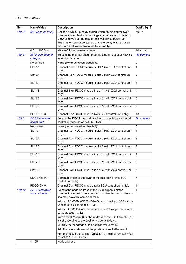
162 Parameters
160.31 M/F wake up delay Defines a wake-up delay during which no master/follower communication faults or warnings are generated. This is to allow all drives on the master/follower link to power up.The master cannot be started until the delay elapses or all monitored followers are found to be ready.
60.0 s
0.0 … 180.0 s Master/follower wake-up delay. 10 = 1 s
160.41 Extension adapter com port
Selects the channel used for connecting an optional FEA-xx extension adapter.
No connect
No connect None (communication disabled). 0
Slot 1A Channel A on FDCO module in slot 1 (with ZCU control unit only).
1
Slot 2A Channel A on FDCO module in slot 2 (with ZCU control unit only).
2
Slot 3A Channel A on FDCO module in slot 3 (with ZCU control unit only).
3
Slot 1B Channel B on FDCO module in slot 1 (with ZCU control unit only).
4
Slot 2B Channel B on FDCO module in slot 2 (with ZCU control unit only).
5
Slot 3B Channel B on FDCO module in slot 3 (with ZCU control unit only).
6
RDCO CH 3 Channel 3 on RDCO module (with BCU control unit only). 13
160.51 DDCS controller comm port
Selects the DDCS channel used for connecting an external controller (such as an AC500 PLC).
No connect
No connect None (communication disabled). 0
Slot 1A Channel A on FDCO module in slot 1 (with ZCU control unit only).
1
Slot 2A Channel A on FDCO module in slot 2 (with ZCU control unit only).
2
Slot 3A Channel A on FDCO module in slot 3 (with ZCU control unit only).
3
Slot 1B Channel B on FDCO module in slot 1 (with ZCU control unit only).
4
Slot 2B Channel B on FDCO module in slot 2 (with ZCU control unit only).
5
Slot 3B Channel B on FDCO module in slot 3 (with ZCU control unit only).
6
DDCS via BC Communication to the inverter module active (with ZCU control unit only).
7
RDCO CH 0 Channel 0 on RDCO module (with BCU control unit only). 11
160.52 DDCS controller node address
Selects the node address of the IGBT supply unit for communication with the external controller. No two nodes on-line may have the same address.
With an AC 800M (CI858) DriveBus connection, IGBT supply units must be addressed 1…24.
With an AC 80 DriveBus connection, IGBT supply units must be addressed 1…12.
With optical ModuleBus, the address of the IGBT supply unit is set according to the position value as follows:
Multiply the hundreds of the position value by 16.
Add the tens and ones of the position value to the result.
For example, if the position value is 101, this parameter must be set to 1×16 + 1 = 17.
1
1…254 Node address.
No. Name/Value Description Def/FbEq16

Parameters 163
160.55 DDCS controller HW connection
Selects the topology of the fiber optic link. Star
Ring The devices are connected in a ring topology. Forwarding of messages is enabled.
0
Star The devices are connected in a star topology (for example, through a branching unit). Forwarding of messages is disabled.
1
160.56 DDCS controller baud rate
Defines the communication speed on the fiber optic link. This should be set to the same value on all devices on the link.
4 Mbps
1 Mbps 1 Mbps. 1
2 Mbps 2 Mbps. 2
4 Mbps 4 Mbps. 4
8 Mbps 8 Mbps. 8
160.57 DDCS controller link control
Defines the light intensity of the transmission LED of RDCO module channel CH0. (This parameter is effective only when parameter 160.51 DDCS controller comm port is set to RDCO CH 0. FDCO modules have a hardware transmitter current selector.)In general, use higher values with longer fiber optic cables. The maximum setting is applicable to the maximum length of the fiber optic link.
10
1…15 Light intensity. 1 = 1
160.58 DDCS controller comm loss time
Sets a timeout for communication with the external controller. If a communication break lasts longer than the timeout, the action specified by parameter 160.59 DDCS controller comm loss function is taken.
100 ms
0…60000 ms Timeout for communication with external controller. 1 = 1 ms
160.59 DDCS controller comm loss function
Selects how the IGBT supply unit reacts to a communication break between it and the external controller.
Fault
No action No action taken. 0
Fault A fault is generated. 1
Warning A warning is generated. 2
160.60 DDCS controller ref1 type
Selects the type and scaling of reference 1 received from the external controller. The resulting value is shown by parameter 103.11 DDCS controller ref 1.
Auto
Auto Type and scaling is chosen automatically according to the currently active control mode.
0
Transparent No scaling is applied. 1
General Generic reference without a specific unit. 2
Frequency Reserved. 5
DC voltage The scaling is defined by parameter 146.04 DC voltage scaling.
8
Active power The scaling is defined by parameter 146.01 Power scaling. 9
Reactive power The scaling is defined by parameter 146.02 Reactive power scaling.
10
AC Voltage Reserved. 13
160.61 DDCS controller ref2 type
Selects the type and scaling of reference 2 received from the external controller. The resulting value is shown by parameter 103.12 DDCS controller ref 2. For the selections, see parameter 160.60 DDCS controller ref1 type.
Auto
160.62 DDCS controller act1 type
Selects the type and scaling of actual value 1 transmitted to the external controller. For the selections, see parameter 160.60 DDCS controller ref1 type.
Auto
No. Name/Value Description Def/FbEq16
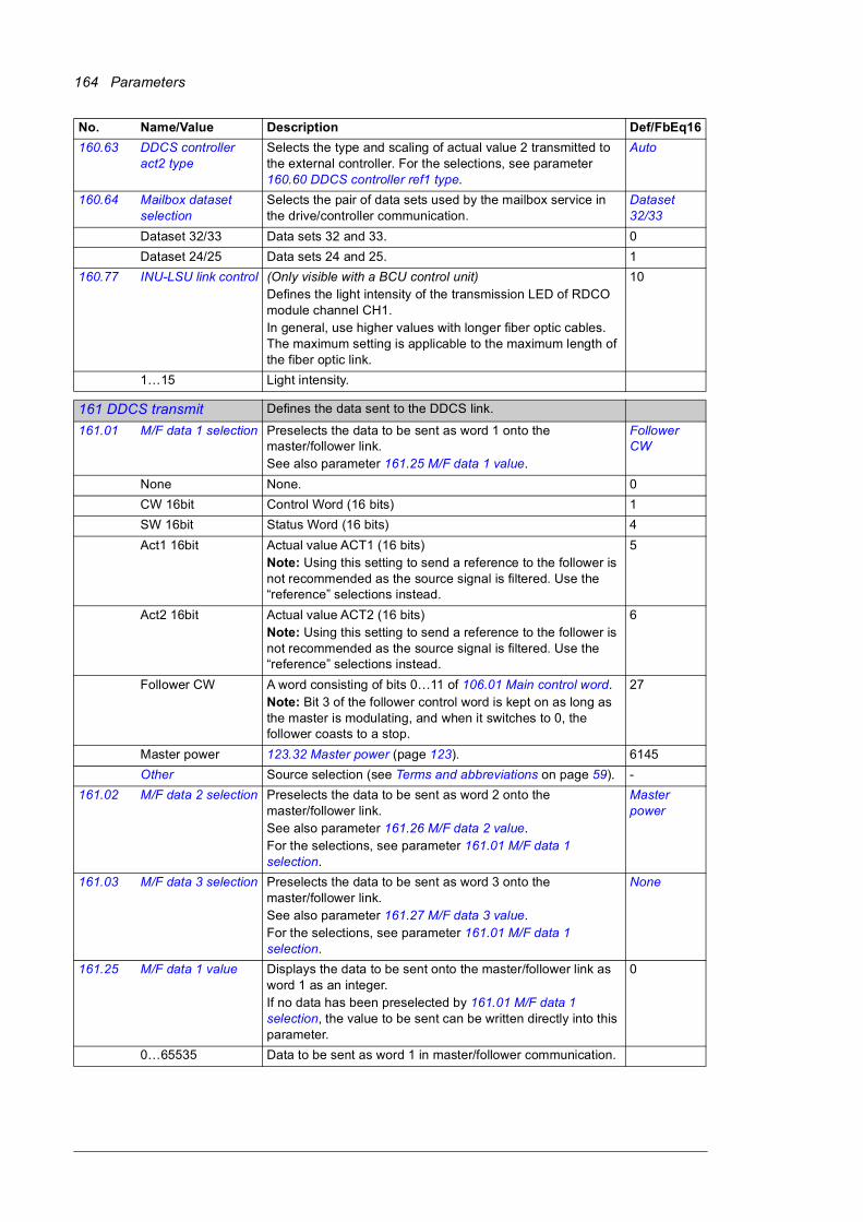
164 Parameters
160.63 DDCS controller act2 type
Selects the type and scaling of actual value 2 transmitted to the external controller. For the selections, see parameter 160.60 DDCS controller ref1 type.
Auto
160.64 Mailbox dataset selection
Selects the pair of data sets used by the mailbox service in the drive/controller communication.
Dataset 32/33
Dataset 32/33 Data sets 32 and 33. 0
Dataset 24/25 Data sets 24 and 25. 1
160.77 INU-LSU link control (Only visible with a BCU control unit)Defines the light intensity of the transmission LED of RDCO module channel CH1.In general, use higher values with longer fiber optic cables. The maximum setting is applicable to the maximum length of the fiber optic link.
10
1…15 Light intensity.
161161 DDCS transmit Defines the data sent to the DDCS link.
161.01 M/F data 1 selection Preselects the data to be sent as word 1 onto the master/follower link.See also parameter 161.25 M/F data 1 value.
Follower CW
None None. 0
CW 16bit Control Word (16 bits) 1
SW 16bit Status Word (16 bits) 4
Act1 16bit Actual value ACT1 (16 bits)Note: Using this setting to send a reference to the follower is not recommended as the source signal is filtered. Use the “reference” selections instead.
5
Act2 16bit Actual value ACT2 (16 bits)Note: Using this setting to send a reference to the follower is not recommended as the source signal is filtered. Use the “reference” selections instead.
6
Follower CW A word consisting of bits 0…11 of 106.01 Main control word.Note: Bit 3 of the follower control word is kept on as long as the master is modulating, and when it switches to 0, the follower coasts to a stop.
27
Master power 123.32 Master power (page 123). 6145
Other Source selection (see Terms and abbreviations on page 59). -
161.02 M/F data 2 selection Preselects the data to be sent as word 2 onto the master/follower link.See also parameter 161.26 M/F data 2 value.For the selections, see parameter 161.01 M/F data 1 selection.
Master power
161.03 M/F data 3 selection Preselects the data to be sent as word 3 onto the master/follower link.See also parameter 161.27 M/F data 3 value.For the selections, see parameter 161.01 M/F data 1 selection.
None
161.25 M/F data 1 value Displays the data to be sent onto the master/follower link as word 1 as an integer.If no data has been preselected by 161.01 M/F data 1 selection, the value to be sent can be written directly into this parameter.
0
0…65535 Data to be sent as word 1 in master/follower communication.
No. Name/Value Description Def/FbEq16
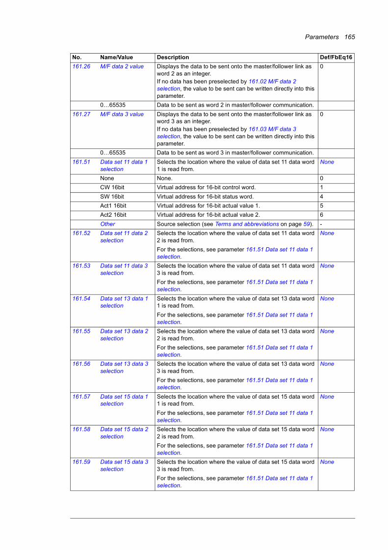
Parameters 165
161.26 M/F data 2 value Displays the data to be sent onto the master/follower link as word 2 as an integer.If no data has been preselected by 161.02 M/F data 2 selection, the value to be sent can be written directly into this parameter.
0
0…65535 Data to be sent as word 2 in master/follower communication.
161.27 M/F data 3 value Displays the data to be sent onto the master/follower link as word 3 as an integer.If no data has been preselected by 161.03 M/F data 3 selection, the value to be sent can be written directly into this parameter.
0
0…65535 Data to be sent as word 3 in master/follower communication.
161.51 Data set 11 data 1 selection
Selects the location where the value of data set 11 data word 1 is read from.
None
None None. 0
CW 16bit Virtual address for 16-bit control word. 1
SW 16bit Virtual address for 16-bit status word. 4
Act1 16bit Virtual address for 16-bit actual value 1. 5
Act2 16bit Virtual address for 16-bit actual value 2. 6
Other Source selection (see Terms and abbreviations on page 59). -
161.52 Data set 11 data 2 selection
Selects the location where the value of data set 11 data word 2 is read from.
For the selections, see parameter 161.51 Data set 11 data 1 selection.
None
161.53 Data set 11 data 3 selection
Selects the location where the value of data set 11 data word 3 is read from.
For the selections, see parameter 161.51 Data set 11 data 1 selection.
None
161.54 Data set 13 data 1 selection
Selects the location where the value of data set 13 data word 1 is read from.
For the selections, see parameter 161.51 Data set 11 data 1 selection.
None
161.55 Data set 13 data 2 selection
Selects the location where the value of data set 13 data word 2 is read from.
For the selections, see parameter 161.51 Data set 11 data 1 selection.
None
161.56 Data set 13 data 3 selection
Selects the location where the value of data set 13 data word 3 is read from.
For the selections, see parameter 161.51 Data set 11 data 1 selection.
None
161.57 Data set 15 data 1 selection
Selects the location where the value of data set 15 data word 1 is read from.
For the selections, see parameter 161.51 Data set 11 data 1 selection.
None
161.58 Data set 15 data 2 selection
Selects the location where the value of data set 15 data word 2 is read from.
For the selections, see parameter 161.51 Data set 11 data 1 selection.
None
161.59 Data set 15 data 3 selection
Selects the location where the value of data set 15 data word 3 is read from.
For the selections, see parameter 161.51 Data set 11 data 1 selection.
None
No. Name/Value Description Def/FbEq16

166 Parameters
161.60 Data set 17 data 1 selection
Selects the location where the value of data set 17 data word 1 is read from.
For the selections, see parameter 161.51 Data set 11 data 1 selection.
None
161.61 Data set 17 data 2 selection
Selects the location where the value of data set 17 data word 2 is read from.
For the selections, see parameter 161.51 Data set 11 data 1 selection.
None
161.62 Data set 17 data 3 selection
Selects the location where the value of data set 17 data word 3 is read from.
For the selections, see parameter 161.51 Data set 11 data 1 selection.
None
161.63 Data set 19 data 1 selection
Selects the location where the value of data set 19 data word 1 is read from.
For the selections, see parameter 161.51 Data set 11 data 1 selection.
None
161.64 Data set 19 data 2 selection
Selects the location where the value of data set 19 data word 2 is read from.
For the selections, see parameter 161.51 Data set 11 data 1 selection.
None
161.65 Data set 19 data 3 selection
Selects the location where the value of data set 19 data word 3 is read from.
For the selections, see parameter 161.51 Data set 11 data 1 selection.
None
161.66 Data set 21 data 1 selection
Selects the location where the value of data set 21 data word 1 is read from.
For the selections, see parameter 161.51 Data set 11 data 1 selection.
None
161.67 Data set 21 data 2 selection
Selects the location where the value of data set 21 data word 2 is read from.
For the selections, see parameter 161.51 Data set 11 data 1 selection.
None
161.68 Data set 21 data 3 selection
Selects the location where the value of data set 21 data word 3 is read from.
For the selections, see parameter 161.51 Data set 11 data 1 selection.
None
161.69 Data set 23 data 1 selection
Selects the location where the value of data set 23 data word 1 is read from.
For the selections, see parameter 161.51 Data set 11 data 1 selection.
None
161.70 Data set 23 data 2 selection
Selects the location where the value of data set 23 data word 2 is read from.
For the selections, see parameter 161.51 Data set 11 data 1 selection.
None
161.71 Data set 23 data 3 selection
Selects the location where the value of data set 23 data word 3 is read from.
For the selections, see parameter 161.51 Data set 11 data 1 selection.
None
161.72 Data set 25 data 1 selection
Selects the location where the value of data set 25 data word 1 is read from.
For the selections, see parameter 161.51 Data set 11 data 1 selection.
None
No. Name/Value Description Def/FbEq16

Parameters 167
161.73 Data set 25 data 2 selection
Selects the location where the value of data set 25 data word 2 is read from.
For the selections, see parameter 161.51 Data set 11 data 1 selection.
None
161.74 Data set 25 data 3 selection
Selects the location where the value of data set 25 data word 3 is read from.
For the selections, see parameter 161.51 Data set 11 data 1 selection.
None
161.101 Data set 11 data 1 value
Defines the raw data to be transmitted in data set 11 data word 1.
-
0…65535 Raw data to be transmitted in data set 11 data word 1. 1 = 1
161.102 Data set 11 data 2 value
Defines the raw data to be transmitted in data set 11 data word 2.
-
0…65535 Raw data to be transmitted in data set 11 data word 2. 1 = 1
161.103 Data set 11 data 3 value
Defines the raw data to be transmitted in data set 11 data word 3.
-
0…65535 Raw data to be transmitted in data set 11 data word 3. 1 = 1
161.104 Data set 13 data 1 value
Defines the raw data to be transmitted in data set 13 data word 1.
-
0…65535 Raw data to be transmitted in data set 13 data word 1. 1 = 1
161.105 Data set 13 data 2 value
Defines the raw data to be transmitted in data set 13 data word 2.
-
0…65535 Raw data to be transmitted in data set 13 data word 2. 1 = 1
161.106 Data set 13 data 3 value
Defines the raw data to be transmitted in data set 13 data word 3.
-
0…65535 Raw data to be transmitted in data set 13 data word 3. 1 = 1
161.107 Data set 15 data 1 value
Defines the raw data to be transmitted in data set 15 data word 1.
-
0…65535 Raw data to be transmitted in data set 15 data word 1. 1 = 1
161.108 Data set 15 data 2 value
Defines the raw data to be transmitted in data set 15 data word 2.
-
0…65535 Raw data to be transmitted in data set 15 data word 2. 1 = 1
161.109 Data set 15 data 3 value
Defines the raw data to be transmitted in data set 15 data word 3.
-
0…65535 Raw data to be transmitted in data set 15 data word 3. 1 = 1
161.110 Data set 17 data 1 value
Defines the raw data to be transmitted in data set 17 data word 1.
-
0…65535 Raw data to be transmitted in data set 17 data word 1. 1 = 1
161.111 Data set 17 data 2 value
Defines the raw data to be transmitted in data set 17 data word 2.
-
0…65535 Raw data to be transmitted in data set 17 data word 2. 1 = 1
161.112 Data set 17 data 3 value
Defines the raw data to be transmitted in data set 17 data word 3.
-
0…65535 Raw data to be transmitted in data set 17 data word 3. 1 = 1
161.113 Data set 19 data 1 value
Defines the raw data to be transmitted in data set 19 data word 1.
-
0…65535 Raw data to be transmitted in data set 19 data word 1. 1 = 1
161.114 Data set 19 data 2 value
Defines the raw data to be transmitted in data set 19 data word 2.
-
0…65535 Raw data to be transmitted in data set 19 data word 2. 1 = 1
161.115 Data set 19 data 3 value
Defines the raw data to be transmitted in data set 19 data word 3.
-
0…65535 Raw data to be transmitted in data set 19 data word 3. 1 = 1
No. Name/Value Description Def/FbEq16

168 Parameters
161.116 Data set 21 data 1 value
Defines the raw data to be transmitted in data set 21 data word 1.
-
0…65535 Raw data to be transmitted in data set 21 data word 1. 1 = 1
161.117 Data set 21 data 2 value
Defines the raw data to be transmitted in data set 21 data word 2.
-
0…65535 Raw data to be transmitted in data set 21 data word 2. 1 = 1
161.118 Data set 21 data 3 value
Defines the raw data to be transmitted in data set 21 data word 3.
-
0…65535 Raw data to be transmitted in data set 21 data word 3. 1 = 1
161.119 Data set 23 data 1 value
Defines the raw data to be transmitted in data set 23 data word 1.
-
0…65535 Raw data to be transmitted in data set 23 data word 1. 1 = 1
161.120 Data set 23 data 2 value
Defines the raw data to be transmitted in data set 23 data word 2.
-
0…65535 Raw data to be transmitted in data set 23 data word 2. 1 = 1
161.121 Data set 23 data 3 value
Defines the raw data to be transmitted in data set 23 data word 3.
-
0…65535 Raw data to be transmitted in data set 23 data word 3. 1 = 1
161.122 Data set 25 data 1 value
Defines the raw data to be transmitted in data set 25 data word 1.
-
0…65535 Raw data to be transmitted in data set 25 data word 1. 1 = 1
161.123 Data set 25 data 2 value
Defines the raw data to be transmitted in data set 25 data word 2.
-
0…65535 Raw data to be transmitted in data set 25 data word 2. 1 = 1
161.124 Data set 25 data 3 value
Defines the raw data to be transmitted in data set 25 data word 3.
-
0…65535 Raw data to be transmitted in data set 25 data word 3. 1 = 1
162162 DDCS receive Mapping of data received through the DDCS link.
162.01 M/F data 1 selection (Follower only) Defines a target for the data received as word 1 from the master through the master/follower link.See also parameter 162.25 MF data 1 value.
None
None None. 0
CW 16bit Control Word (16 bits) 1
Ref1 16bit Reference REF1 (16 bits) 2
Ref2 16bit Reference REF2 (16 bits) 3
Master power 123.32 Master power (page 123). 6145
Other Source selection (see Terms and abbreviations on page 59). -
162.02 M/F data 2 selection (Follower only) Defines a target for the data received as word 2 from the master through the master/follower link.See also parameter 162.26 MF data 2 value.For the selections, see parameter 162.01 M/F data 1 selection.
None
162.03 M/F data 3 selection (Follower only) Defines a target for the data received as word 3 from the master through the master/follower link.See also parameter 162.27 MF data 3 value.For the selections, see parameter 162.01 M/F data 1 selection.
None
162.04 Follower node 2 data 1 sel
Defines a target for the data received as word 1 from the first follower (ie. the follower with node address 2) through the master/follower link.See also parameter 162.28 Follower node 2 data 1 value.
Follower SW
None None. 0
No. Name/Value Description Def/FbEq16
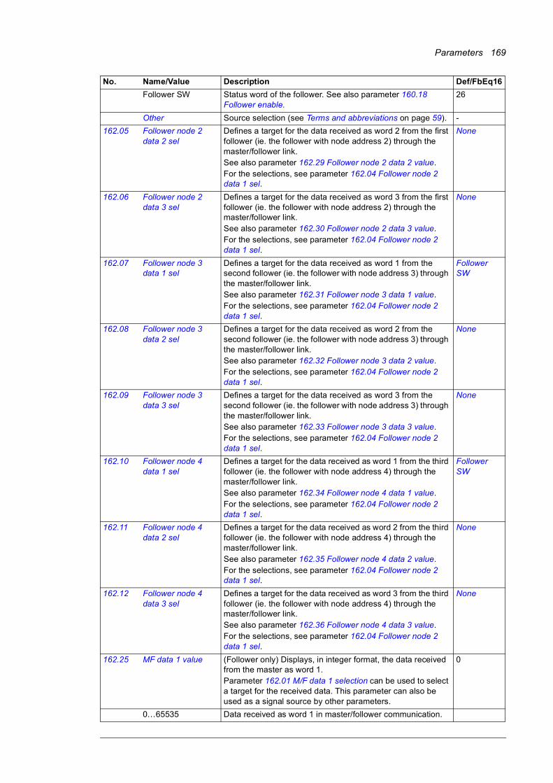
Parameters 169
Follower SW Status word of the follower. See also parameter 160.18 Follower enable.
26
Other Source selection (see Terms and abbreviations on page 59). -
162.05 Follower node 2 data 2 sel
Defines a target for the data received as word 2 from the first follower (ie. the follower with node address 2) through the master/follower link.See also parameter 162.29 Follower node 2 data 2 value.For the selections, see parameter 162.04 Follower node 2 data 1 sel.
None
162.06 Follower node 2 data 3 sel
Defines a target for the data received as word 3 from the first follower (ie. the follower with node address 2) through the master/follower link.See also parameter 162.30 Follower node 2 data 3 value.For the selections, see parameter 162.04 Follower node 2 data 1 sel.
None
162.07 Follower node 3 data 1 sel
Defines a target for the data received as word 1 from the second follower (ie. the follower with node address 3) through the master/follower link.See also parameter 162.31 Follower node 3 data 1 value.For the selections, see parameter 162.04 Follower node 2 data 1 sel.
Follower SW
162.08 Follower node 3 data 2 sel
Defines a target for the data received as word 2 from the second follower (ie. the follower with node address 3) through the master/follower link.See also parameter 162.32 Follower node 3 data 2 value.For the selections, see parameter 162.04 Follower node 2 data 1 sel.
None
162.09 Follower node 3 data 3 sel
Defines a target for the data received as word 3 from the second follower (ie. the follower with node address 3) through the master/follower link.See also parameter 162.33 Follower node 3 data 3 value.For the selections, see parameter 162.04 Follower node 2 data 1 sel.
None
162.10 Follower node 4 data 1 sel
Defines a target for the data received as word 1 from the third follower (ie. the follower with node address 4) through the master/follower link.See also parameter 162.34 Follower node 4 data 1 value.For the selections, see parameter 162.04 Follower node 2 data 1 sel.
Follower SW
162.11 Follower node 4 data 2 sel
Defines a target for the data received as word 2 from the third follower (ie. the follower with node address 4) through the master/follower link.See also parameter 162.35 Follower node 4 data 2 value.For the selections, see parameter 162.04 Follower node 2 data 1 sel.
None
162.12 Follower node 4 data 3 sel
Defines a target for the data received as word 3 from the third follower (ie. the follower with node address 4) through the master/follower link.See also parameter 162.36 Follower node 4 data 3 value.For the selections, see parameter 162.04 Follower node 2 data 1 sel.
None
162.25 MF data 1 value (Follower only) Displays, in integer format, the data received from the master as word 1.Parameter 162.01 M/F data 1 selection can be used to select a target for the received data. This parameter can also be used as a signal source by other parameters.
0
0…65535 Data received as word 1 in master/follower communication.
No. Name/Value Description Def/FbEq16

170 Parameters
162.26 MF data 2 value (Follower only) Displays, in integer format, the data received from the master as word 2.Parameter 162.02 M/F data 2 selection can be used to select a target for the received data. This parameter can also be used as a signal source by other parameters.
0
0…65535 Data received as word 2 in master/follower communication.
162.27 MF data 3 value (Follower only) Displays, in integer format, the data received from the master as word 3.Parameter 162.03 M/F data 3 selection can be used to select a target for the received data. This parameter can also be used as a signal source by other parameters.
0
0…65535 Data received as word 3 in master/follower communication.
162.28 Follower node 2 data 1 value
Displays, in integer format, the data received from the first follower (ie. follower with node address 2) as word 1.Parameter 162.04 Follower node 2 data 1 sel can be used to select a target for the received data. This parameter can also be used as a signal source by other parameters.
0
0…65535 Data received as word 1 from follower with node address 2.
162.29 Follower node 2 data 2 value
Displays, in integer format, the data received from the first follower (ie. follower with node address 2) as word 2.Parameter 162.05 Follower node 2 data 2 sel can be used to select a target for the received data. This parameter can also be used as a signal source by other parameters.
0
0…65535 Data received as word 2 from follower with node address 2.
162.30 Follower node 2 data 3 value
Displays, in integer format, the data received from the first follower (ie. follower with node address 2) as word 3.Parameter 162.06 Follower node 2 data 3 sel can be used to select a target for the received data. This parameter can also be used as a signal source by other parameters.
0
0…65535 Data received as word 3 from follower with node address 2.
162.31 Follower node 3 data 1 value
Displays, in integer format, the data received from the second follower (ie. follower with node address 3) as word 1.Parameter 162.07 Follower node 3 data 1 sel can be used to select a target for the received data. This parameter can also be used as a signal source by other parameters.
0
0…65535 Data received as word 1 from follower with node address 3.
162.32 Follower node 3 data 2 value
Displays, in integer format, the data received from the second follower (ie. follower with node address 3) as word 2.Parameter 162.08 Follower node 3 data 2 sel can be used to select a target for the received data. This parameter can also be used as a signal source by other parameters.
0
0…65535 Data received as word 2 from follower with node address 3.
162.33 Follower node 3 data 3 value
Displays, in integer format, the data received from the second follower (ie. follower with node address 3) as word 3.Parameter 162.09 Follower node 3 data 3 sel can be used to select a target for the received data. This parameter can also be used as a signal source by other parameters.
0
0…65535 Data received as word 3 from follower with node address 3.
162.34 Follower node 4 data 1 value
Displays, in integer format, the data received from the third follower (ie. follower with node address 4) as word 1.Parameter 162.10 Follower node 4 data 1 sel can be used to select a target for the received data. This parameter can also be used as a signal source by other parameters.
0
0…65535 Data received as word 1 from follower with node address 4.
No. Name/Value Description Def/FbEq16
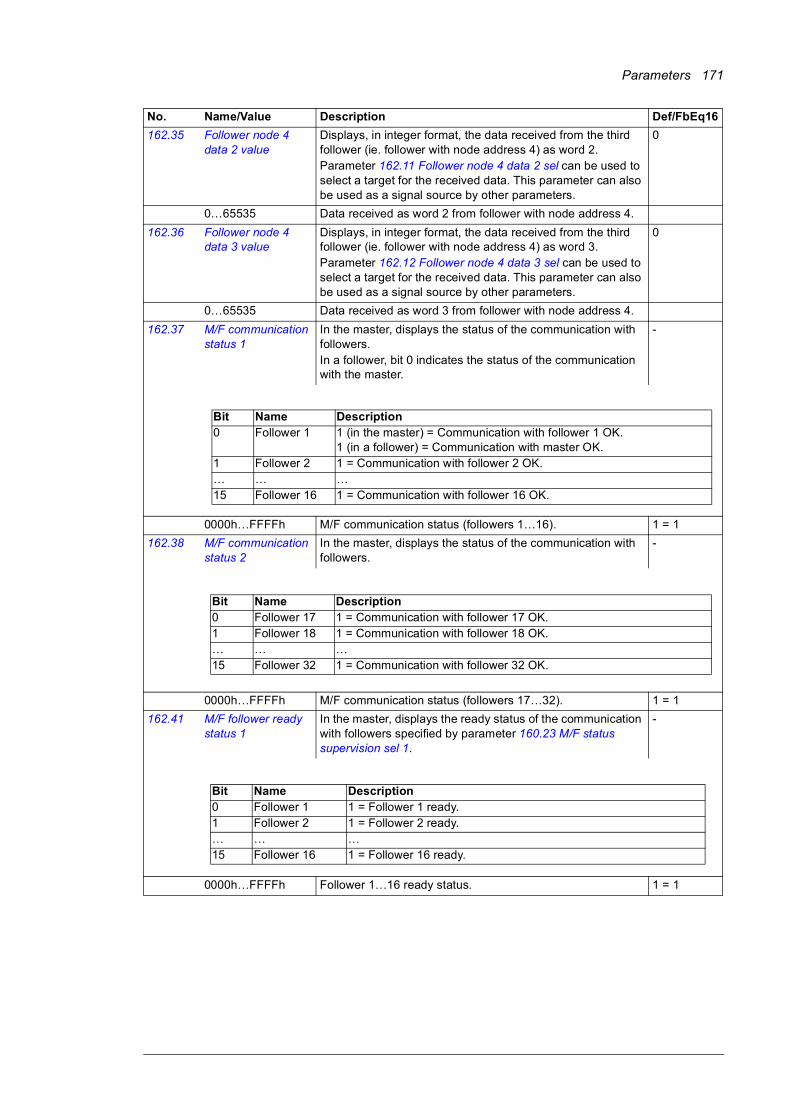
Parameters 171
162.35 Follower node 4 data 2 value
Displays, in integer format, the data received from the third follower (ie. follower with node address 4) as word 2.Parameter 162.11 Follower node 4 data 2 sel can be used to select a target for the received data. This parameter can also be used as a signal source by other parameters.
0
0…65535 Data received as word 2 from follower with node address 4.
162.36 Follower node 4 data 3 value
Displays, in integer format, the data received from the third follower (ie. follower with node address 4) as word 3.Parameter 162.12 Follower node 4 data 3 sel can be used to select a target for the received data. This parameter can also be used as a signal source by other parameters.
0
0…65535 Data received as word 3 from follower with node address 4.
162.37 M/F communication status 1
In the master, displays the status of the communication with followers.In a follower, bit 0 indicates the status of the communication with the master.
-
0000h…FFFFh M/F communication status (followers 1…16). 1 = 1
162.38 M/F communication status 2
In the master, displays the status of the communication with followers.
-
0000h…FFFFh M/F communication status (followers 17…32). 1 = 1
162.41 M/F follower ready status 1
In the master, displays the ready status of the communication with followers specified by parameter 160.23 M/F status supervision sel 1.
-
0000h…FFFFh Follower 1…16 ready status. 1 = 1
No. Name/Value Description Def/FbEq16
Bit Name Description0 Follower 1 1 (in the master) = Communication with follower 1 OK.
1 (in a follower) = Communication with master OK.1 Follower 2 1 = Communication with follower 2 OK.… … …15 Follower 16 1 = Communication with follower 16 OK.
Bit Name Description0 Follower 17 1 = Communication with follower 17 OK.1 Follower 18 1 = Communication with follower 18 OK.… … …15 Follower 32 1 = Communication with follower 32 OK.
Bit Name Description0 Follower 1 1 = Follower 1 ready.1 Follower 2 1 = Follower 2 ready.… … …15 Follower 16 1 = Follower 16 ready.

172 Parameters
162.42 M/F follower ready status 2
In the master, displays the ready status of the communication with followers.
-
0000h…FFFFh Follower 17…32 ready status. 1 = 1
162.51 Data set 10 data 1 selection
Selects the location into which the value of data set 10 data word 1 is written.
None
None None. 0
CW 16bit Virtual address for 16-bit control word. 1
Ref1 16bit Virtual address for 16-bit reference 1. 2
Ref2 16bit Virtual address for 16-bit reference 2. 3
Other Source selection (see Terms and abbreviations on page 59). -
162.52 Data set 10 data 2 selection
Selects the location into which the value of data set 10 data word 2 is written.
For the selections, see parameter 162.51 Data set 10 data 1 selection.
None
162.53 Data set 10 data 3 selection
Selects the location into which the value of data set 10 data word 3 is written.
For the selections, see parameter 162.51 Data set 10 data 1 selection.
None
162.54 Data set 12 data 1 selection
Selects the location into which the value of data set 12 data word 1 is written.
For the selections, see parameter 162.51 Data set 10 data 1 selection.
None
162.55 Data set 12 data 2 selection
Selects the location into which the value of data set 12 data word 2 is written.
For the selections, see parameter 162.51 Data set 10 data 1 selection.
None
162.56 Data set 12 data 3 selection
Selects the location into which the value of data set 12 data word 3 is written.
For the selections, see parameter 162.51 Data set 10 data 1 selection.
None
162.57 Data set 14 data 1 selection
Selects the location into which the value of data set 14 data word 1 is written.
For the selections, see parameter 162.51 Data set 10 data 1 selection.
None
162.58 Data set 14 data 2 selection
Selects the location into which the value of data set 14 data word 2 is written.
For the selections, see parameter 162.51 Data set 10 data 1 selection.
None
162.59 Data set 14 data 3 selection
Selects the location into which the value of data set 14 data word 3 is written.
For the selections, see parameter 162.51 Data set 10 data 1 selection.
None
162.60 Data set 16 data 1 selection
Selects the location into which the value of data set 16 data word 1 is written.
For the selections, see parameter 162.51 Data set 10 data 1 selection.
None
No. Name/Value Description Def/FbEq16
Bit Name Description0 Follower 17 1 = Follower 17 ready.1 Follower 18 1 = Follower 18 ready.… … …15 Follower 32 1 = Follower 32 ready.
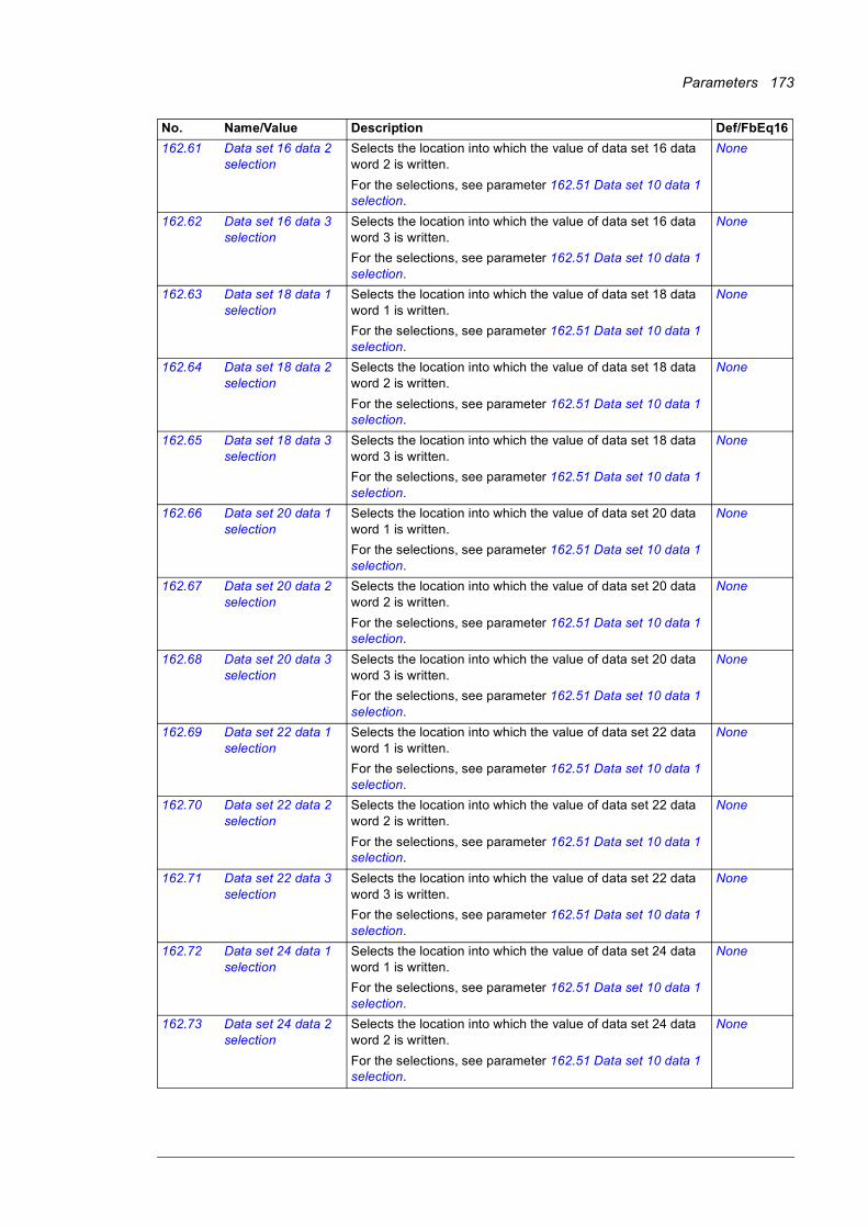
Parameters 173
162.61 Data set 16 data 2 selection
Selects the location into which the value of data set 16 data word 2 is written.
For the selections, see parameter 162.51 Data set 10 data 1 selection.
None
162.62 Data set 16 data 3 selection
Selects the location into which the value of data set 16 data word 3 is written.
For the selections, see parameter 162.51 Data set 10 data 1 selection.
None
162.63 Data set 18 data 1 selection
Selects the location into which the value of data set 18 data word 1 is written.
For the selections, see parameter 162.51 Data set 10 data 1 selection.
None
162.64 Data set 18 data 2 selection
Selects the location into which the value of data set 18 data word 2 is written.
For the selections, see parameter 162.51 Data set 10 data 1 selection.
None
162.65 Data set 18 data 3 selection
Selects the location into which the value of data set 18 data word 3 is written.
For the selections, see parameter 162.51 Data set 10 data 1 selection.
None
162.66 Data set 20 data 1 selection
Selects the location into which the value of data set 20 data word 1 is written.
For the selections, see parameter 162.51 Data set 10 data 1 selection.
None
162.67 Data set 20 data 2 selection
Selects the location into which the value of data set 20 data word 2 is written.
For the selections, see parameter 162.51 Data set 10 data 1 selection.
None
162.68 Data set 20 data 3 selection
Selects the location into which the value of data set 20 data word 3 is written.
For the selections, see parameter 162.51 Data set 10 data 1 selection.
None
162.69 Data set 22 data 1 selection
Selects the location into which the value of data set 22 data word 1 is written.
For the selections, see parameter 162.51 Data set 10 data 1 selection.
None
162.70 Data set 22 data 2 selection
Selects the location into which the value of data set 22 data word 2 is written.
For the selections, see parameter 162.51 Data set 10 data 1 selection.
None
162.71 Data set 22 data 3 selection
Selects the location into which the value of data set 22 data word 3 is written.
For the selections, see parameter 162.51 Data set 10 data 1 selection.
None
162.72 Data set 24 data 1 selection
Selects the location into which the value of data set 24 data word 1 is written.
For the selections, see parameter 162.51 Data set 10 data 1 selection.
None
162.73 Data set 24 data 2 selection
Selects the location into which the value of data set 24 data word 2 is written.
For the selections, see parameter 162.51 Data set 10 data 1 selection.
None
No. Name/Value Description Def/FbEq16

174 Parameters
162.74 Data set 24 data 3 selection
Selects the location into which the value of data set 24 data word 3 is written.
For the selections, see parameter 162.51 Data set 10 data 1 selection.
None
162.101 Data set 10 data 1 value
Defines the raw data to be received in data set 10 data word 1.
-
0…65535 Raw data to be received in data set 10 data word 1. 1 = 1
162.102 Data set 10 data 2 value
Defines the raw data to be received in data set 10 data word 2.
-
0…65535 Raw data to be received in data set 10 data word 2. 1 = 1
162.103 Data set 10 data 3 value
Defines the raw data to be received in data set 10 data word 3.
-
0…65535 Raw data to be received in data set 10 data word 3. 1 = 1
162.104 Data set 12 data 1 value
Defines the raw data to be received in data set 12 data word 1.
-
0…65535 Raw data to be received in data set 12 data word 1. 1 = 1
162.105 Data set 12 data 2 value
Defines the raw data to be received in data set 12 data word 2.
-
0…65535 Raw data to be received in data set 12 data word 2. 1 = 1
162.106 Data set 12 data 3 value
Defines the raw data to be received in data set 12 data word 3.
-
0…65535 Raw data to be received in data set 12 data word 3. 1 = 1
162.107 Data set 14 data 1 value
Defines the raw data to be received in data set 14 data word 1.
-
0…65535 Raw data to be received in data set 14 data word 1. 1 = 1
162.108 Data set 14 data 2 value
Defines the raw data to be received in data set 14 data word 2.
-
0…65535 Raw data to be received in data set 14 data word 2. 1 = 1
162.109 Data set 14 data 3 value
Defines the raw data to be received in data set 14 data word 3.
-
0…65535 Raw data to be received in data set 14 data word 3. 1 = 1
162.110 Data set 16 data 1 value
Defines the raw data to be received in data set 16 data word 1.
-
0…65535 Raw data to be received in data set 16 data word 1. 1 = 1
162.111 Data set 16 data 2 value
Defines the raw data to be received in data set 16 data word 2.
-
0…65535 Raw data to be received in data set 16 data word 2. 1 = 1
162.112 Data set 16 data 3 value
Defines the raw data to be received in data set 16 data word 3.
-
0…65535 Raw data to be received in data set 16 data word 3. 1 = 1
162.113 Data set 18 data 1 value
Defines the raw data to be received in data set 18 data word 1.
-
0…65535 Raw data to be received in data set 18 data word 1. 1 = 1
162.114 Data set 18 data 2 value
Defines the raw data to be received in data set 18 data word 2.
-
0…65535 Raw data to be received in data set 18 data word 2. 1 = 1
162.115 Data set 18 data 3 value
Defines the raw data to be received in data set 18 data word 3.
-
0…65535 Raw data to be received in data set 18 data word 3. 1 = 1
162.116 Data set 20 data 1 value
Defines the raw data to be received in data set 20 data word 1.
-
0…65535 Raw data to be received in data set 20 data word 1. 1 = 1
No. Name/Value Description Def/FbEq16

Parameters 175
162.117 Data set 20 data 2 value
Defines the raw data to be received in data set 20 data word 2.
-
0…65535 Raw data to be received in data set 20 data word 2. 1 = 1
162.118 Data set 20 data 3 value
Defines the raw data to be received in data set 20 data word 3.
-
0…65535 Raw data to be received in data set 20 data word 3. 1 = 1
162.119 Data set 22 data 1 value
Defines the raw data to be received in data set 22 data word 1.
-
0…65535 Raw data to be received in data set 22 data word 1. 1 = 1
162.120 Data set 22 data 2 value
Defines the raw data to be received in data set 22 data word 2.
-
0…65535 Raw data to be received in data set 22 data word 2. 1 = 1
162.121 Data set 22 data 3 value
Defines the raw data to be received in data set 22 data word 3.
-
0…65535 Raw data to be received in data set 22 data word 3. 1 = 1
162.122 Data set 24 data 1 value
Defines the raw data to be received in data set 24 data word 1.
-
0…65535 Raw data to be received in data set 24 data word 1. 1 = 1
162.123 Data set 24 data 2 value
Defines the raw data to be received in data set 24 data word 2.
-
0…65535 Raw data to be received in data set 24 data word 2. 1 = 1
162.124 Data set 24 data 3 value
Defines the raw data to be received in data set 24 data word 3.
-
0…65535 Raw data to be received in data set 24 data word 3. 1 = 1
190190 BAMU measurements Grid measurement signals from BAMU measurement unit.
BAMU measures voltages and currents configured in parameter group 191 BAMU configuration.
All parameters in this group are read-only.
190.01 Phase voltage U1 Shows the RMS value of phase voltage U1a. -
0.00…2000.00 V RMS value of phase voltage U1a. 1 = 1 V
190.02 Phase voltage V1 Shows the RMS value of phase voltage U1b. -
0.00…2000.00 V RMS value of phase voltage U1b. 1 = 1 V
190.03 Phase voltage W1 Shows the RMS value of phase voltage U1c. -
0.00…2000.00 V RMS value of phase voltage U1c. 1 = 1 V
190.06 Mains voltage U1-V1
Shows the RMS value of line-to-line voltage U1ab. -
0.00…2000.00 V RMS value of line-to-line voltage U1ab. 1 = 1 V
190.07 Mains voltage V1-W1
Shows the RMS value of line-to-line voltage U1bc. -
0.00…2000.00 V RMS value of line-to-line voltage U1bc. 1 = 1 V
190.08 Mains voltage W1-U1
Shows the RMS value of line-to-line voltage U1ca. -
0.00…2000.00 V RMS value of line-to-line voltage U1ca. 1 = 1 V
190.15 Frequency 1 Shows the frequency of the measured voltage U1. -
0.00…100.00 Hz Frequency of the measured voltage U1. 1 = 1 Hz
190.20 Phase voltage U2 Shows the RMS value of phase voltage U2a. -
0.00…2000.00 V RMS value of phase voltage U2a. 1 = 1 V
190.21 Phase voltage V2 Shows the RMS value of phase voltage U2b. -
0.00…2000.00 V RMS value of phase voltage U2b. 1 = 1 V
190.22 Phase voltage W2 Shows the RMS value of phase voltage U2c. -
0.00…2000.00 V RMS value of phase voltage U2c. 1 = 1 V
No. Name/Value Description Def/FbEq16

176 Parameters
190.25 Mains voltage U2-V2
Shows the RMS value of line-to-line voltage U2ab. -
0.00…2000.00 V RMS value of line-to-line voltage U2ab. 1 = 1 V
190.26 Mains voltage V2-W2
Shows the RMS value of line-to-line voltage U2bc. -
0.00…2000.00 V RMS value of line-to-line voltage U2bc. 1 = 1 V
190.27 Mains voltage W2-U2
Shows the RMS value of line-to-line voltage U2ca. -
0.00…2000.00 V RMS value of line-to-line voltage U2ca. 1 = 1 V
190.34 Frequency 2 Shows the frequency of the measured voltage U2. -
0.00…100.00 Hz Frequency of the measured voltage U2. 1 = 1 Hz
190.40 Phase current U1 Shows the RMS value of phase current Ia. -
- RMS value of phase current Ia. 1 = 1 A
190.41 Phase current V1 Shows the RMS value of phase current Ib. -
- RMS value of phase current Ib. 1 = 1 A
190.42 Phase current W1 Shows the RMS value of phase current Ic. -
- RMS value of phase current Ic. 1 = 1 A
191191 BAMU configuration Settings for BAMU measurement unit.
191.01 U1 measurement Enables U1 measurements. No
No U1 measurements disabled. 0
Yes U1 measurements enabled. 1
191.02 U1 meas type Selects U1 voltage measurement type. For more information on BAMU board measurements, see BAMU-12C auxiliary measurement unit hardware manual (3AXD50000117840 [English]).
Mains voltage
Mains voltage Main voltage measurement. 1
Phase voltage Voltage measurement against phase ground. 2
Phase voltage neutral
Voltage measurement against virtual ground. 3
191.05 U1 measurement location
Selects the measurement location for voltage U1. CB converter side
CB converter side Voltage U1 is measured on the converter-side of main circuit breaker.
0
CB grid side Voltage U1 is measured on the grid-side of main circuit breaker.
1
191.10 U2 measurement Enables U2 measurements. No
No U2 measurements disabled. 0
Yes U2 measurements enabled. 1
No. Name/Value Description Def/FbEq16
BAMUU1
CB converter side CB grid side
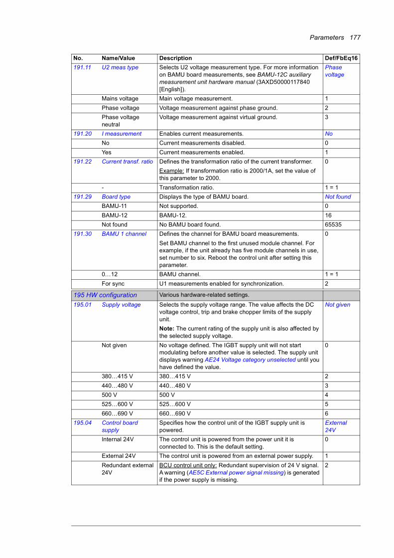
Parameters 177
191.11 U2 meas type Selects U2 voltage measurement type. For more information on BAMU board measurements, see BAMU-12C auxiliary measurement unit hardware manual (3AXD50000117840 [English]).
Phase voltage
Mains voltage Main voltage measurement. 1
Phase voltage Voltage measurement against phase ground. 2
Phase voltage neutral
Voltage measurement against virtual ground. 3
191.20 I measurement Enables current measurements. No
No Current measurements disabled. 0
Yes Current measurements enabled. 1
191.22 Current transf. ratio Defines the transformation ratio of the current transformer.
Example: If transformation ratio is 2000/1A, set the value of this parameter to 2000.
0
- Transformation ratio. 1 = 1
191.29 Board type Displays the type of BAMU board. Not found
BAMU-11 Not supported. 0
BAMU-12 BAMU-12. 16
Not found No BAMU board found. 65535
191.30 BAMU 1 channel Defines the channel for BAMU board measurements.
Set BAMU channel to the first unused module channel. For example, if the unit already has five module channels in use, set number to six. Reboot the control unit after setting this parameter.
0
0…12 BAMU channel. 1 = 1
For sync U1 measurements enabled for synchronization. 2
195195 HW configuration Various hardware-related settings.
195.01 Supply voltage Selects the supply voltage range. The value affects the DC voltage control, trip and brake chopper limits of the supply unit.
Note: The current rating of the supply unit is also affected by the selected supply voltage.
Not given
Not given No voltage defined. The IGBT supply unit will not start modulating before another value is selected. The supply unit displays warning AE24 Voltage category unselected until you have defined the value.
0
380…415 V 380…415 V 2
440…480 V 440…480 V 3
500 V 500 V 4
525…600 V 525…600 V 5
660…690 V 660…690 V 6
195.04 Control board supply
Specifies how the control unit of the IGBT supply unit is powered.
External 24V
Internal 24V The control unit is powered from the power unit it is connected to. This is the default setting.
0
External 24V The control unit is powered from an external power supply. 1
Redundant external 24V
BCU control unit only: Redundant supervision of 24 V signal. A warning (AE5C External power signal missing) is generated if the power supply is missing.
2
No. Name/Value Description Def/FbEq16
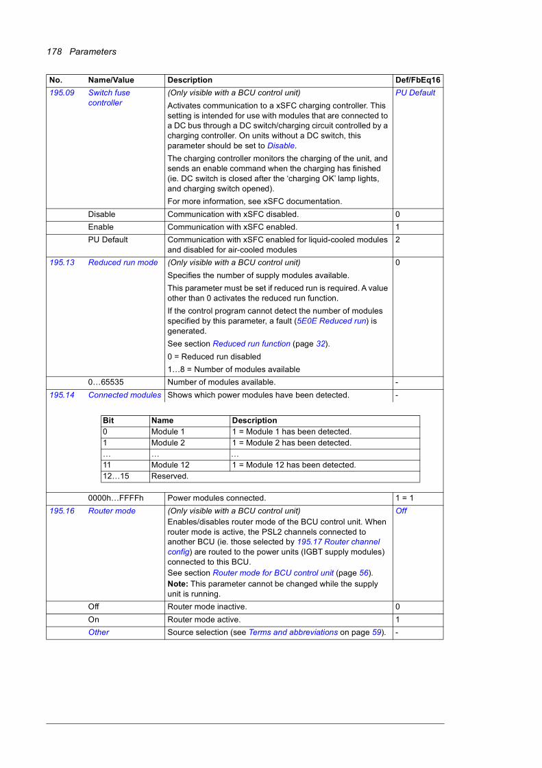
178 Parameters
195.09 Switch fuse controller
(Only visible with a BCU control unit)
Activates communication to a xSFC charging controller. This setting is intended for use with modules that are connected to a DC bus through a DC switch/charging circuit controlled by a charging controller. On units without a DC switch, this parameter should be set to Disable.
The charging controller monitors the charging of the unit, and sends an enable command when the charging has finished (ie. DC switch is closed after the ‘charging OK’ lamp lights, and charging switch opened).
For more information, see xSFC documentation.
PU Default
Disable Communication with xSFC disabled. 0
Enable Communication with xSFC enabled. 1
PU Default Communication with xSFC enabled for liquid-cooled modules and disabled for air-cooled modules
2
195.13 Reduced run mode (Only visible with a BCU control unit)
Specifies the number of supply modules available.
This parameter must be set if reduced run is required. A value other than 0 activates the reduced run function.
If the control program cannot detect the number of modules specified by this parameter, a fault (5E0E Reduced run) is generated.
See section Reduced run function (page 32).
0 = Reduced run disabled
1…8 = Number of modules available
0
0…65535 Number of modules available. -
195.14 Connected modules Shows which power modules have been detected. -
0000h…FFFFh Power modules connected. 1 = 1
195.16 Router mode (Only visible with a BCU control unit)Enables/disables router mode of the BCU control unit. When router mode is active, the PSL2 channels connected to another BCU (ie. those selected by 195.17 Router channel config) are routed to the power units (IGBT supply modules) connected to this BCU.See section Router mode for BCU control unit (page 56).Note: This parameter cannot be changed while the supply unit is running.
Off
Off Router mode inactive. 0
On Router mode active. 1
Other Source selection (see Terms and abbreviations on page 59). -
No. Name/Value Description Def/FbEq16
Bit Name Description0 Module 1 1 = Module 1 has been detected.1 Module 2 1 = Module 2 has been detected.… … …11 Module 12 1 = Module 12 has been detected.12…15 Reserved.
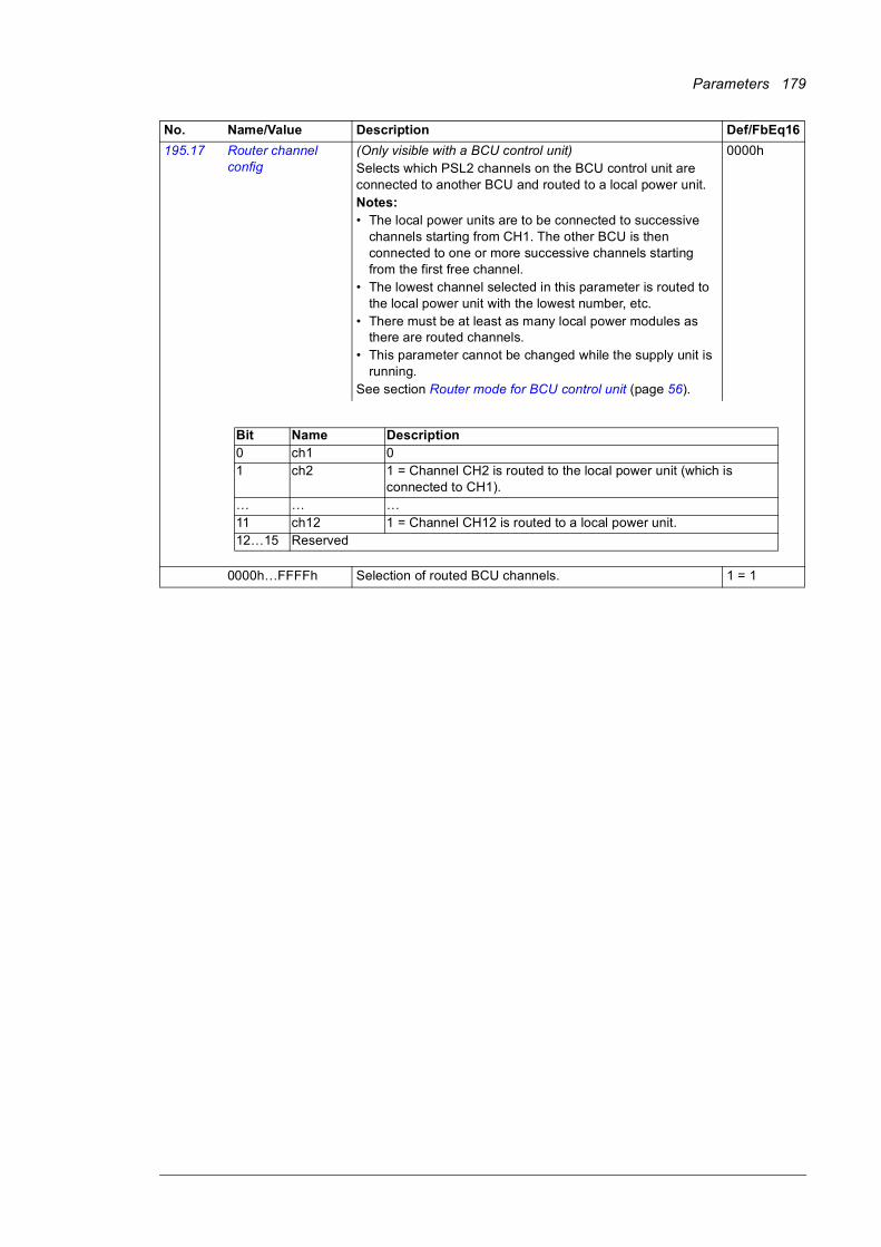
Parameters 179
195.17 Router channel config
(Only visible with a BCU control unit)Selects which PSL2 channels on the BCU control unit are connected to another BCU and routed to a local power unit.Notes:• The local power units are to be connected to successive
channels starting from CH1. The other BCU is then connected to one or more successive channels starting from the first free channel.
• The lowest channel selected in this parameter is routed to the local power unit with the lowest number, etc.
• There must be at least as many local power modules as there are routed channels.
• This parameter cannot be changed while the supply unit is running.
See section Router mode for BCU control unit (page 56).
0000h
0000h…FFFFh Selection of routed BCU channels. 1 = 1
No. Name/Value Description Def/FbEq16
Bit Name Description0 ch1 01 ch2 1 = Channel CH2 is routed to the local power unit (which is
connected to CH1).… … …11 ch12 1 = Channel CH12 is routed to a local power unit.12…15 Reserved
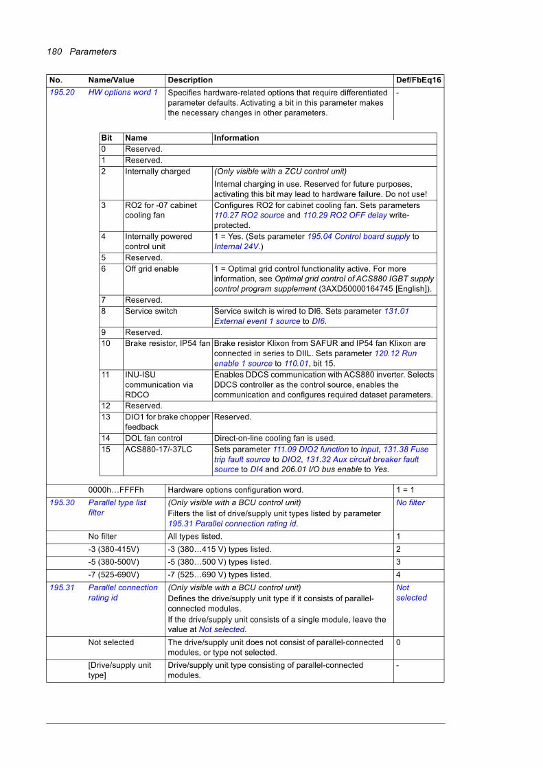
180 Parameters
195.20 HW options word 1 Specifies hardware-related options that require differentiated parameter defaults. Activating a bit in this parameter makes the necessary changes in other parameters.
-
0000h…FFFFh Hardware options configuration word. 1 = 1
195.30 Parallel type list filter
(Only visible with a BCU control unit)Filters the list of drive/supply unit types listed by parameter 195.31 Parallel connection rating id.
No filter
No filter All types listed. 1
-3 (380-415V) -3 (380…415 V) types listed. 2
-5 (380-500V) -5 (380…500 V) types listed. 3
-7 (525-690V) -7 (525…690 V) types listed. 4
195.31 Parallel connection rating id
(Only visible with a BCU control unit)Defines the drive/supply unit type if it consists of parallel-connected modules.If the drive/supply unit consists of a single module, leave the value at Not selected.
Not selected
Not selected The drive/supply unit does not consist of parallel-connected modules, or type not selected.
0
[Drive/supply unit type]
Drive/supply unit type consisting of parallel-connected modules.
-
No. Name/Value Description Def/FbEq16
Bit Name Information0 Reserved.1 Reserved.2 Internally charged (Only visible with a ZCU control unit)
Internal charging in use. Reserved for future purposes, activating this bit may lead to hardware failure. Do not use!
3 RO2 for -07 cabinet cooling fan
Configures RO2 for cabinet cooling fan. Sets parameters 110.27 RO2 source and 110.29 RO2 OFF delay write-protected.
4 Internally powered control unit
1 = Yes. (Sets parameter 195.04 Control board supply to Internal 24V.)
5 Reserved.6 Off grid enable 1 = Optimal grid control functionality active. For more
information, see Optimal grid control of ACS880 IGBT supply control program supplement (3AXD50000164745 [English]).
7 Reserved.8 Service switch Service switch is wired to DI6. Sets parameter 131.01
External event 1 source to DI6.9 Reserved.10 Brake resistor, IP54 fan Brake resistor Klixon from SAFUR and IP54 fan Klixon are
connected in series to DIIL. Sets parameter 120.12 Run enable 1 source to 110.01, bit 15.
11 INU-ISU communication via RDCO
Enables DDCS communication with ACS880 inverter. Selects DDCS controller as the control source, enables the communication and configures required dataset parameters.
12 Reserved.13 DIO1 for brake chopper
feedbackReserved.
14 DOL fan control Direct-on-line cooling fan is used.15 ACS880-17/-37LC Sets parameter 111.09 DIO2 function to Input, 131.38 Fuse
trip fault source to DIO2, 131.32 Aux circuit breaker fault source to DI4 and 206.01 I/O bus enable to Yes.

Parameters 181
195.51 Current offset calibration
Disables/enables the current offset calibration. In calibration, the current is measured and averaged for 500 ms. Measured value is considered as current offset and it is reduced from actual measurement values.Automatic mode is strongly recommended if AC mode is used. Otherwise default selection No is recommended.
No
No Disabled. 0
Automatic Automatic current offset calibration is enabled. 1
196196 System Language selection; parameter save and restore; control unit
reboot; user lock.
196.01 Language Selects the language of the parameter interface and other displayed information.
Not selected
Not selected None. 0
English English. 1033
196.02 Pass code Pass codes can be entered into this parameter to activate further access levels (see parameter 196.03 Access levels active) or to configure the user lock.
Entering “358” toggles the parameter lock, which prevents the changing of all other parameters through the control panel or the Drive composer PC tool.
Entering the user pass code (by default, “10000000”) enables parameters 196.100…196.102, which can be used to define a new user pass code and to select the actions that are to be prevented.
Entering an invalid pass code will close the user lock if open, ie. hide parameters 196.100…196.102. After entering the code, check that the parameters are in fact hidden. If they are not, enter another (random) pass code.
Entering several invalid pass codes introduces a delay before a new attempt can be made. Entering further invalid codes will progressively lengthen the delay.
Note: You must change the default user pass code to maintain a high level of cybersecurity. Store the code in a safe place – the protection cannot be disabled even by ABB if the code is lost.
See also section User lock (page 40).
1
0…99999999 Pass code. 1 = 1
196.03 Access levels active Shows which access levels have been activated by pass codes entered into parameter 196.02 Pass code.
001b
000b…111b Active access levels. -
196.06 Parameter restore Restores the original settings of the control program, ie. parameter default values.
Note: This parameter cannot be changed while the IGBT supply unit is running.
Done
Done Restoring is completed. 0
No. Name/Value Description Def/FbEq16
Bit Name0 End user1 Service2 Advanced users3…13 Reserved.14 Parameter lock15 Reserved.

182 Parameters
Restore defaults All editable parameter values are restored to default values, except
• I/O extension module settings
• control panel/PC communication settings
• fieldbus adapter settings
• parameter 195.01 Supply voltage
• parameter 195.20 HW options word 1 and the differentiated defaults implemented by it.
8
Clear all All editable parameter values are restored to default values, except
• control panel/PC communication settings
• parameter 195.01 Supply voltage
• parameter 195.20 HW options word 1 and the differentiated defaults implemented by it.
PC tool communication is interrupted during the restoring.
62
Reset all fieldbussettings
Fieldbus adapter settings (parameter groups 150…156) are restored to default values. This will also restore the default settings of the fieldbus adapter if one is connected.
32
196.07 Parameter save manually
Saves the valid parameter values to memory.
Note: A new parameter value is saved automatically when changed from the PC tool or panel but not when altered through a fieldbus adapter connection.
Done
Done Save completed. 0
Save Save in progress. 1
196.08 Control board boot Changing the value of this parameter to 1 reboots the control unit. The value reverts to 0 automatically.
0
0…1 1 = Reboot control unit. 1 = 1
196.10 User set status Shows the status of the user parameter sets.
This parameter is read-only.
See also section User parameter sets (page 39).
n/a
n/a No user parameter sets have been saved. 0
Loading A user set is being loaded. 1
Saving A user set is being saved. 2
Faulted Invalid or empty parameter set. 3
User set 1 User set 1 has been loaded. 4
User set 2 User set 2 has been loaded. 5
User set 3 User set 3 has been loaded. 6
User set 4 User set 4 has been loaded. 7
No. Name/Value Description Def/FbEq16
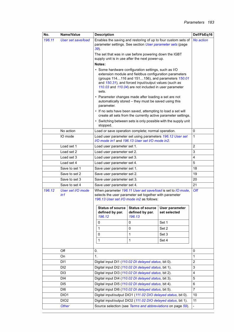
Parameters 183
196.11 User set save/load Enables the saving and restoring of up to four custom sets of parameter settings. See section User parameter sets (page 39).
The set that was in use before powering down the IGBT supply unit is in use after the next power-up.
Notes:
• Some hardware configuration settings, such as I/O extension module and fieldbus configuration parameters (groups 114…116 and 151…156), and parameters 150.01 and 150.31), and forced input/output values (such as 110.03 and 110.04) are not included in user parameter sets.
• Parameter changes made after loading a set are not automatically stored – they must be saved using this parameter.
• If no sets have been saved, attempting to load a set will create all sets from the currently active parameter settings.
• Switching between sets is only possible with the supply unit stopped.
No action
No action Load or save operation complete; normal operation. 0
IO mode Load user parameter set using parameters 196.12 User set I/O mode in1 and 196.13 User set I/O mode in2.
1
Load set 1 Load user parameter set 1. 2
Load set 2 Load user parameter set 2. 3
Load set 3 Load user parameter set 3. 4
Load set 4 Load user parameter set 4. 5
Save to set 1 Save user parameter set 1. 18
Save to set 2 Save user parameter set 2. 19
Save to set 3 Save user parameter set 3. 20
Save to set 4 Save user parameter set 4. 21
196.12 User set I/O mode in1
When parameter 196.11 User set save/load is set to IO mode, selects the user parameter set together with parameter 196.13 User set I/O mode in2 as follows:
Off
Off 0. 0
On 1. 1
DI1 Digital input DI1 (110.02 DI delayed status, bit 0). 2
DI2 Digital input DI2 (110.02 DI delayed status, bit 1). 3
DI3 Digital input DI3 (110.02 DI delayed status, bit 2). 4
DI4 Digital input DI4 (110.02 DI delayed status, bit 3). 5
DI5 Digital input DI5 (110.02 DI delayed status, bit 4). 6
DI6 Digital input DI6 (110.02 DI delayed status, bit 5). 7
DIO1 Digital input/output DIO1 (111.02 DIO delayed status, bit 0). 10
DIO2 Digital input/output DIO2 (111.02 DIO delayed status, bit 1). 11
Other Source selection (see Terms and abbreviations on page 59). -
No. Name/Value Description Def/FbEq16
Status of source defined by par. 196.12
Status of source defined by par. 196.13
User parameter set selected
0 0 Set 1
1 0 Set 2
0 1 Set 3
1 1 Set 4

184 Parameters
196.13 User set I/O mode in2
See parameter 196.12 User set I/O mode in1. Off
196.20 Time sync primary source
Defines the 1st priority external source for synchronization of the unit’s time and date.
DDCS Controller
Internal No external source selected. 0
DDCS Controller External controller. 1
Fieldbus A or B Fieldbus interface A or B. 2
Fieldbus A Fieldbus interface A. 3
Fieldbus B Fieldbus interface B. 4
D2D or M/F The master station on a master/follower or drive-to-drive link. 5
Panel link Control panel, or Drive composer PC tool connected to the control panel.
8
Ethernet tool link Drive composer PC tool through an FENA-xx module. 9
FA2FA Another control program. 10
196.24 Full days since 1st Jan 1980
Number of full days passed since beginning of the year 1980.
This parameter, together with 196.25 Time in minutes within 24 h and 196.26 Time in ms within one minute makes it possible to set the date and time in the drive via the parameter interface from a fieldbus or application program. This may be necessary if the fieldbus protocol does not support time synchronization.
-
1…59999 Days since beginning of 1980. 1 = 1
196.25 Time in minutes within 24 h
Number of full minutes passed since midnight. For example, the value 860 corresponds to 2:20 pm.
See parameter 196.24 Full days since 1st Jan 1980.
0 min
1…1439 Minutes since midnight. 1 = 1
196.26 Time in ms within one minute
Number of milliseconds passed since last minute.
See parameter 196.24 Full days since 1st Jan 1980.
0 ms
0…59999 Number of milliseconds since last minute. 1 = 1
No. Name/Value Description Def/FbEq16

Parameters 185
196.29 Time sync source status
Time source status word.
This parameter is read-only.
-
0000h…FFFFh Time source status word 1. 1 = 1
196.39 Power up event logging
Enables/disables power-up logging. When enabled, an event (BE08 Power up) is logged by the IGBT supply unit upon each power-up.
Enable
Disable Power-up event logging disabled. 0
Enable Power-up event logging enabled. 1
196.61 User data logger status word
Provides status information on the user data logger (see page 221).
0000b
0000b…1111b User data logger status word. 1 = 1
No. Name/Value Description Def/FbEq16
Bit Name Description0 Time tick received 1 = 1st priority tick received: Tick has been received from 1st
priority source.1 Aux Time tick received 1 = 2nd priority tick received: Tick has been received from
2nd priority source.2 Tick interval is too long 1 = Yes: Tick interval too long (accuracy compromised).3 DDCS controller 1 = Tick received: Tick has been received from an external
controller.4 Master/Follower 1 = Tick received: Tick has been received through the
master/follower link.5 Reserved.6 D2D 1 = Tick received: Tick has been received through the drive-
to-drive link.7 FbusA 1 = Tick received: Tick has been received through fieldbus
interface A.8 FbusB 1 = Tick received: Tick has been received through fieldbus
interface B.9 EFB 1 = Tick received: Tick has been received through the
embedded fieldbus interface.10 Reserved.11 Panel link 1 = Tick received: Tick has been received from the control
panel, or Drive composer PC tool connected to the control panel.
12 Ethernet tool link 1 = Tick received: Tick has been received from Drive composer PC tool through an FENA-xx module.
13 Parameter setting 1 = Tick received: Tick has been set by parameters 196.24…196.26.
14 RTC 1 = RTC time in use: Time and date have been read from the real-time clock.
15 Drive On-Time 1 = Drive on-time in use: Time and date are displaying drive on-time.
Bit Name Description0 Running 1 = The user data logger is running. The bit is cleared after the post-
trigger time has passed.1 Triggered 1 = The user data logger has been triggered. The bit is cleared when the
logger is restarted.2 Data
available1 = The user data logger contains data that can be read. Note that the bit is not cleared because the data is saved to the memory unit.
3 Configured 1 = The user data logger has been configured. Note that the bit is not cleared because the configuration data is saved to the memory unit.
4…15 Reserved

186 Parameters
196.63 User data logger trigger
Triggers, or selects a source that triggers, the user data logger.
Off
Off 0. 0
On 1. 1
Other Source selection (see Terms and abbreviations on page 59). -
196.64 User data logger start
Starts, or selects a source that starts, the user data logger. Off
Off 0. 0
On 1. 1
Other Source selection (see Terms and abbreviations on page 59). -
196.65 Factory data logger time level
Selects the sampling interval for the factory data logger (see page 221).
500us
500us 500 microseconds. 500
2ms 2 milliseconds. 2000
10ms 10 milliseconds. 10000
196.70 Disable adaptive program
Enables/disables the adaptive program (if present).See also section Adaptive programming (page 23).
No
No Adaptive program enabled. 0
Yes Adaptive program disabled. 1
196.100 Change user pass code
(Visible when user lock is open)To change the current user pass code, enter a new code into this parameter as well as 196.101 Confirm user pass code. A warning will be active until the new pass code is confirmed. To cancel changing the pass code, close the user lock without confirming. To close the lock, enter an invalid pass code in parameter 196.02 Pass code, activate parameter 196.08 Control board boot, or cycle the power.See also section User lock (page 40).
10000000
10000000…99999999
New user pass code. -
196.101 Confirm user pass code
(Visible when user lock is open)Confirms the new user pass code entered in 196.100 Change user pass code.
10000000…99999999
Confirmation of new user pass code. -
No. Name/Value Description Def/FbEq16
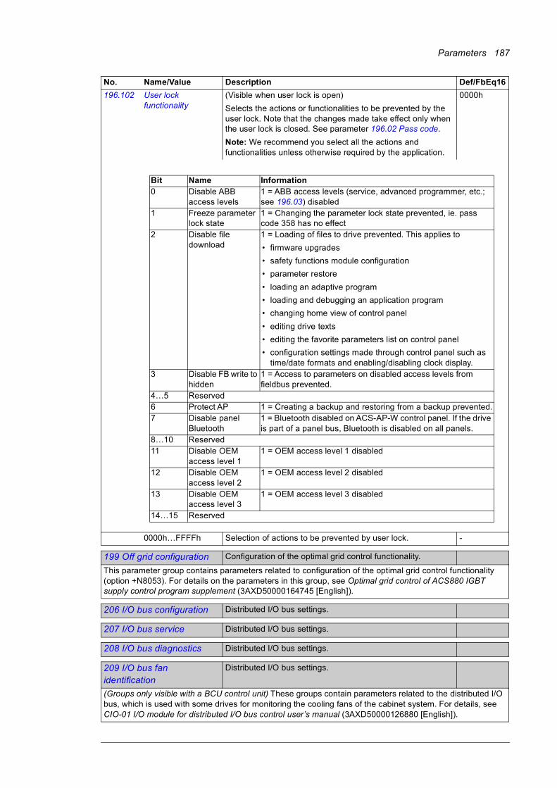
Parameters 187
196.102 User lock functionality
(Visible when user lock is open)
Selects the actions or functionalities to be prevented by the user lock. Note that the changes made take effect only when the user lock is closed. See parameter 196.02 Pass code.
Note: We recommend you select all the actions and functionalities unless otherwise required by the application.
0000h
0000h…FFFFh Selection of actions to be prevented by user lock. -
199199 Off grid configuration Configuration of the optimal grid control functionality.
This parameter group contains parameters related to configuration of the optimal grid control functionality (option +N8053). For details on the parameters in this group, see Optimal grid control of ACS880 IGBT supply control program supplement (3AXD50000164745 [English]).
206206 I/O bus configuration Distributed I/O bus settings.
207207 I/O bus service Distributed I/O bus settings.
208208 I/O bus diagnostics Distributed I/O bus settings.
209209 I/O bus fan identification
Distributed I/O bus settings.
(Groups only visible with a BCU control unit) These groups contain parameters related to the distributed I/O bus, which is used with some drives for monitoring the cooling fans of the cabinet system. For details, see CIO-01 I/O module for distributed I/O bus control user’s manual (3AXD50000126880 [English]).
No. Name/Value Description Def/FbEq16
Bit Name Information0 Disable ABB
access levels1 = ABB access levels (service, advanced programmer, etc.; see 196.03) disabled
1 Freeze parameter lock state
1 = Changing the parameter lock state prevented, ie. pass code 358 has no effect
2 Disable file download
1 = Loading of files to drive prevented. This applies to
• firmware upgrades
• safety functions module configuration
• parameter restore
• loading an adaptive program
• loading and debugging an application program
• changing home view of control panel
• editing drive texts
• editing the favorite parameters list on control panel
• configuration settings made through control panel such as time/date formats and enabling/disabling clock display.
3 Disable FB write to hidden
1 = Access to parameters on disabled access levels from fieldbus prevented.
4…5 Reserved6 Protect AP 1 = Creating a backup and restoring from a backup prevented.7 Disable panel
Bluetooth1 = Bluetooth disabled on ACS-AP-W control panel. If the drive is part of a panel bus, Bluetooth is disabled on all panels.
8…10 Reserved11 Disable OEM
access level 11 = OEM access level 1 disabled
12 Disable OEM access level 2
1 = OEM access level 2 disabled
13 Disable OEM access level 3
1 = OEM access level 3 disabled
14…15 Reserved

188 Parameters

Additional parameter data 189
7
Additional parameter data
What this chapter containsThis chapter lists the parameters with some additional data. For parameter descriptions, see chapter Parameters (page 59).
Terms and abbreviations
Term Definition
Actual signal Signal measured or calculated by the IGBT supply unit. Usually can only be monitored but not adjusted; some counter-type signals can however be reset.
Analog src The parameter can be set to the value of another parameter by choosing “Other”, and selecting the source parameter from a list.
In addition to the “Other” selection, the parameter may offer other pre-selected settings.
Binary src The value of the parameter can be taken from a specific bit in another parameter value (“Other”). Sometimes the value can be fixed to 0 (false) or 1 (true). In addition, the parameter may offer other pre-selected settings.
Data Data parameter.
FbEq32 32-bit fieldbus equivalent: The scaling between the integer used in communication and the value shown on the panel when a 32-bit value is selected for transmission to an external system.
The corresponding 16-bit scalings are listed in chapter Parameters (page 59).
List Selection list.
No. Parameter number.
PB Packed Boolean (bit list).
Real Real number.

190 Additional parameter data
Fieldbus addressesRefer to the User’s manual of the fieldbus adapter.
Type Parameter type. See Analog src, Binary src, List, PB, Real.
Term Definition
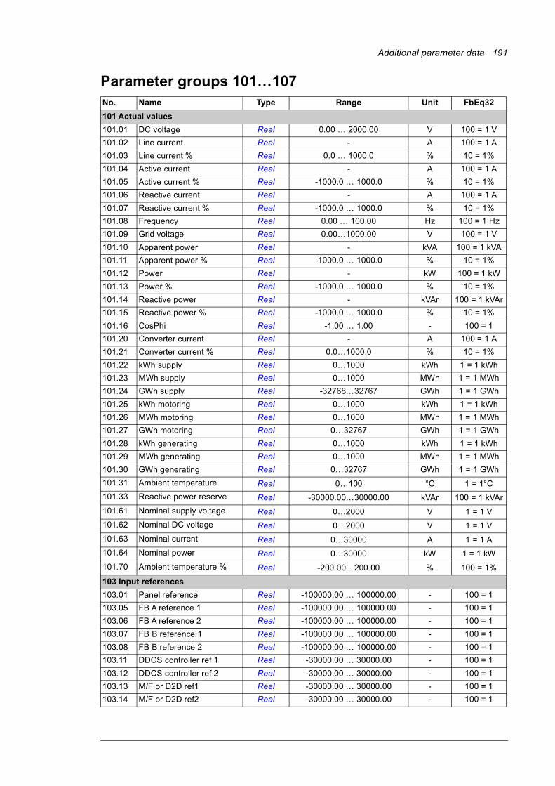
Additional parameter data 191
Parameter groups 101…107No. Name Type Range Unit FbEq32
101 Actual values
101.01 DC voltage Real 0.00 … 2000.00 V 100 = 1 V
101.02 Line current Real - A 100 = 1 A
101.03 Line current % Real 0.0 … 1000.0 % 10 = 1%
101.04 Active current Real - A 100 = 1 A
101.05 Active current % Real -1000.0 … 1000.0 % 10 = 1%
101.06 Reactive current Real - A 100 = 1 A
101.07 Reactive current % Real -1000.0 … 1000.0 % 10 = 1%
101.08 Frequency Real 0.00 … 100.00 Hz 100 = 1 Hz
101.09 Grid voltage Real 0.00…1000.00 V 100 = 1 V
101.10 Apparent power Real - kVA 100 = 1 kVA
101.11 Apparent power % Real -1000.0 … 1000.0 % 10 = 1%
101.12 Power Real - kW 100 = 1 kW
101.13 Power % Real -1000.0 … 1000.0 % 10 = 1%
101.14 Reactive power Real - kVAr 100 = 1 kVAr
101.15 Reactive power % Real -1000.0 … 1000.0 % 10 = 1%
101.16 CosPhi Real -1.00 … 1.00 - 100 = 1
101.20 Converter current Real - A 100 = 1 A
101.21 Converter current % Real 0.0…1000.0 % 10 = 1%
101.22 kWh supply Real 0…1000 kWh 1 = 1 kWh
101.23 MWh supply Real 0…1000 MWh 1 = 1 MWh
101.24 GWh supply Real -32768…32767 GWh 1 = 1 GWh
101.25 kWh motoring Real 0…1000 kWh 1 = 1 kWh
101.26 MWh motoring Real 0…1000 MWh 1 = 1 MWh
101.27 GWh motoring Real 0…32767 GWh 1 = 1 GWh
101.28 kWh generating Real 0…1000 kWh 1 = 1 kWh
101.29 MWh generating Real 0…1000 MWh 1 = 1 MWh
101.30 GWh generating Real 0…32767 GWh 1 = 1 GWh
101.31 Ambient temperature Real 0…100 °C 1 = 1°C
101.33 Reactive power reserve Real -30000.00…30000.00 kVAr 100 = 1 kVAr
101.61 Nominal supply voltage Real 0…2000 V 1 = 1 V
101.62 Nominal DC voltage Real 0…2000 V 1 = 1 V
101.63 Nominal current Real 0…30000 A 1 = 1 A
101.64 Nominal power Real 0…30000 kW 1 = 1 kW
101.70 Ambient temperature % Real -200.00…200.00 % 100 = 1%
103 Input references
103.01 Panel reference Real -100000.00 … 100000.00 - 100 = 1
103.05 FB A reference 1 Real -100000.00 … 100000.00 - 100 = 1
103.06 FB A reference 2 Real -100000.00 … 100000.00 - 100 = 1
103.07 FB B reference 1 Real -100000.00 … 100000.00 - 100 = 1
103.08 FB B reference 2 Real -100000.00 … 100000.00 - 100 = 1
103.11 DDCS controller ref 1 Real -30000.00 … 30000.00 - 100 = 1
103.12 DDCS controller ref 2 Real -30000.00 … 30000.00 - 100 = 1
103.13 M/F or D2D ref1 Real -30000.00 … 30000.00 - 100 = 1
103.14 M/F or D2D ref2 Real -30000.00 … 30000.00 - 100 = 1

192 Additional parameter data
104 Warnings and faults
104.01 Tripping fault Data 0000h…FFFFh - 1 = 1
104.02 Active fault 2 Data 0000h…FFFFh - 1 = 1
104.03 Active fault 3 Data 0000h…FFFFh - 1 = 1
104.04 Active fault 4 Data 0000h…FFFFh - 1 = 1
104.05 Active fault 5 Data 0000h…FFFFh - 1 = 1
104.06 Active warning 1 Data 0000h…FFFFh - 1 = 1
104.07 Active warning 2 Data 0000h…FFFFh - 1 = 1
104.08 Active warning 3 Data 0000h…FFFFh - 1 = 1
104.09 Active warning 4 Data 0000h…FFFFh - 1 = 1
104.10 Active warning 5 Data 0000h…FFFFh - 1 = 1
104.11 Latest fault Data 0000h…FFFFh - 1 = 1
104.12 2nd latest fault Data 0000h…FFFFh - 1 = 1
104.13 3rd latest fault Data 0000h…FFFFh - 1 = 1
104.14 4th latest fault Data 0000h…FFFFh - 1 = 1
104.15 5th latest fault Data 0000h…FFFFh - 1 = 1
104.16 Latest warning Data 0000h…FFFFh - 1 = 1
104.17 2nd latest warning Data 0000h…FFFFh - 1 = 1
104.18 3rd latest warning Data 0000h…FFFFh - 1 = 1
104.19 4th latest warning Data 0000h…FFFFh - 1 = 1
104.20 5th latest warning Data 0000h…FFFFh - 1 = 1
104.21 Fault word 1 Data 0000h…FFFFh - 1 = 1
104.31 Warning word 1 Data 0000h…FFFFh - 1 = 1
104.40 Event word 1 Data 0000h…FFFFh - 1 = 1
104.41 Event word 1 bit 0 code Data 0000h…FFFFh - 1 = 1
104.42 Event word 1 bit 0 aux code
Data 0000h…FFFFh - 1 = 1
104.43 Event word 1 bit 1 code Data 0000h…FFFFh - 1 = 1
104.44 Event word 1 bit 1 aux code
Data 0000h…FFFFh - 1 = 1
104.45 Event word 1 bit 2 code Data 0000h…FFFFh - 1 = 1
104.46 Event word 1 bit 2 aux code
Data 0000h…FFFFh - 1 = 1
104.47 Event word 1 bit 3 code Data 0000h…FFFFh - 1 = 1
104.48 Event word 1 bit 3 aux code
Data 0000h…FFFFh - 1 = 1
104.49 Event word 1 bit 4 code Data 0000h…FFFFh - 1 = 1
104.50 Event word 1 bit 4 aux code
Data 0000h…FFFFh - 1 = 1
104.51 Event word 1 bit 5 code Data 0000h…FFFFh - 1 = 1
104.52 Event word 1 bit 5 aux code
Data 0000h…FFFFh - 1 = 1
104.53 Event word 1 bit 6 code Data 0000h…FFFFh - 1 = 1
104.54 Event word 1 bit 6 aux code
Data 0000h…FFFFh - 1 = 1
104.55 Event word 1 bit 7 code Data 0000h…FFFFh - 1 = 1
104.56 Event word 1 bit 7 aux code
Data 0000h…FFFFh - 1 = 1
104.57 Event word 1 bit 8 code Data 0000h…FFFFh - 1 = 1
104.58 Event word 1 bit 8 aux code
Data 0000h…FFFFh - 1 = 1
No. Name Type Range Unit FbEq32
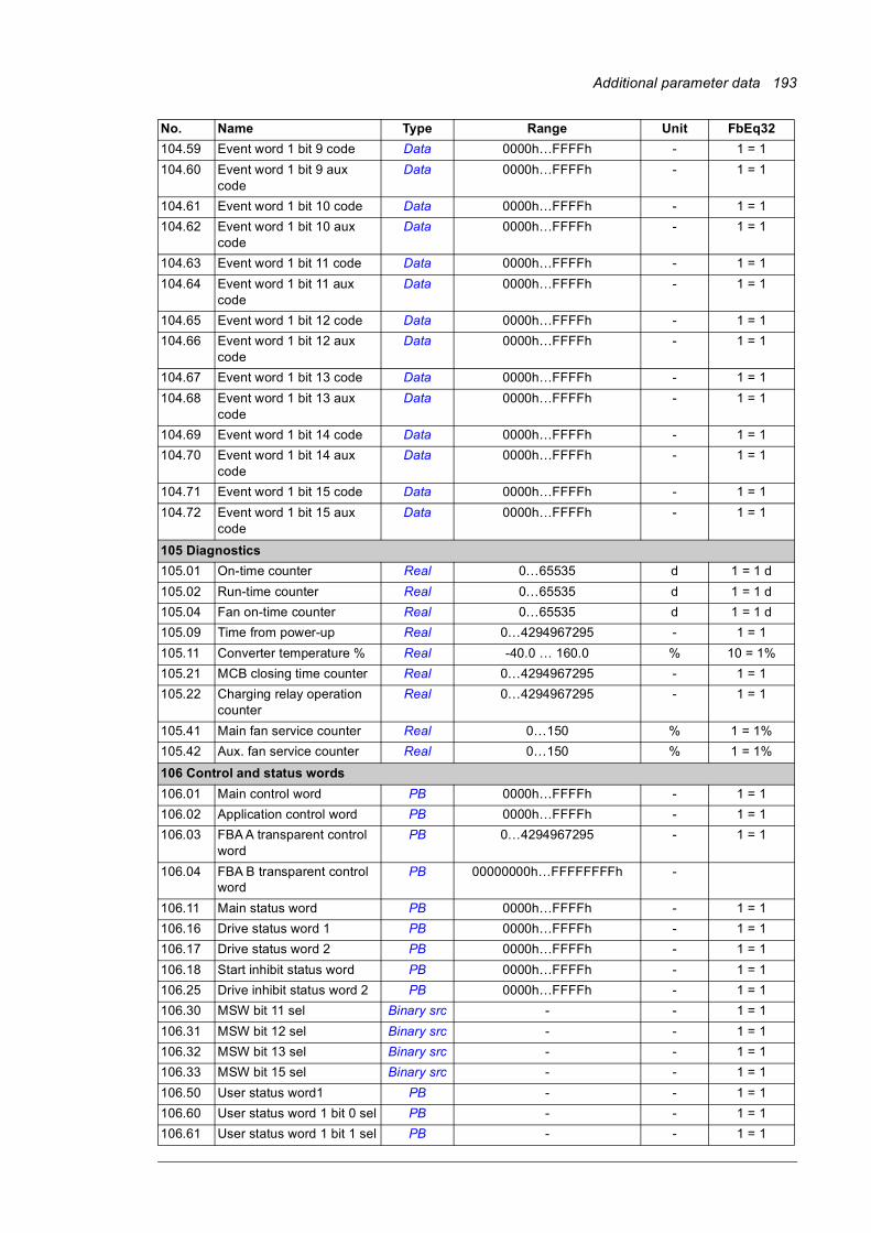
Additional parameter data 193
104.59 Event word 1 bit 9 code Data 0000h…FFFFh - 1 = 1
104.60 Event word 1 bit 9 aux code
Data 0000h…FFFFh - 1 = 1
104.61 Event word 1 bit 10 code Data 0000h…FFFFh - 1 = 1
104.62 Event word 1 bit 10 aux code
Data 0000h…FFFFh - 1 = 1
104.63 Event word 1 bit 11 code Data 0000h…FFFFh - 1 = 1
104.64 Event word 1 bit 11 aux code
Data 0000h…FFFFh - 1 = 1
104.65 Event word 1 bit 12 code Data 0000h…FFFFh - 1 = 1
104.66 Event word 1 bit 12 aux code
Data 0000h…FFFFh - 1 = 1
104.67 Event word 1 bit 13 code Data 0000h…FFFFh - 1 = 1
104.68 Event word 1 bit 13 aux code
Data 0000h…FFFFh - 1 = 1
104.69 Event word 1 bit 14 code Data 0000h…FFFFh - 1 = 1
104.70 Event word 1 bit 14 aux code
Data 0000h…FFFFh - 1 = 1
104.71 Event word 1 bit 15 code Data 0000h…FFFFh - 1 = 1
104.72 Event word 1 bit 15 aux code
Data 0000h…FFFFh - 1 = 1
105 Diagnostics
105.01 On-time counter Real 0…65535 d 1 = 1 d
105.02 Run-time counter Real 0…65535 d 1 = 1 d
105.04 Fan on-time counter Real 0…65535 d 1 = 1 d
105.09 Time from power-up Real 0…4294967295 - 1 = 1
105.11 Converter temperature % Real -40.0 … 160.0 % 10 = 1%
105.21 MCB closing time counter Real 0…4294967295 - 1 = 1
105.22 Charging relay operation counter
Real 0…4294967295 - 1 = 1
105.41 Main fan service counter Real 0…150 % 1 = 1%
105.42 Aux. fan service counter Real 0…150 % 1 = 1%
106 Control and status words
106.01 Main control word PB 0000h…FFFFh - 1 = 1
106.02 Application control word PB 0000h…FFFFh - 1 = 1
106.03 FBA A transparent control word
PB 0…4294967295 - 1 = 1
106.04 FBA B transparent control word
PB 00000000h…FFFFFFFFh -
106.11 Main status word PB 0000h…FFFFh - 1 = 1
106.16 Drive status word 1 PB 0000h…FFFFh - 1 = 1
106.17 Drive status word 2 PB 0000h…FFFFh - 1 = 1
106.18 Start inhibit status word PB 0000h…FFFFh - 1 = 1
106.25 Drive inhibit status word 2 PB 0000h…FFFFh - 1 = 1
106.30 MSW bit 11 sel Binary src - - 1 = 1
106.31 MSW bit 12 sel Binary src - - 1 = 1
106.32 MSW bit 13 sel Binary src - - 1 = 1
106.33 MSW bit 15 sel Binary src - - 1 = 1
106.50 User status word1 PB - - 1 = 1
106.60 User status word 1 bit 0 sel PB - - 1 = 1
106.61 User status word 1 bit 1 sel PB - - 1 = 1
No. Name Type Range Unit FbEq32
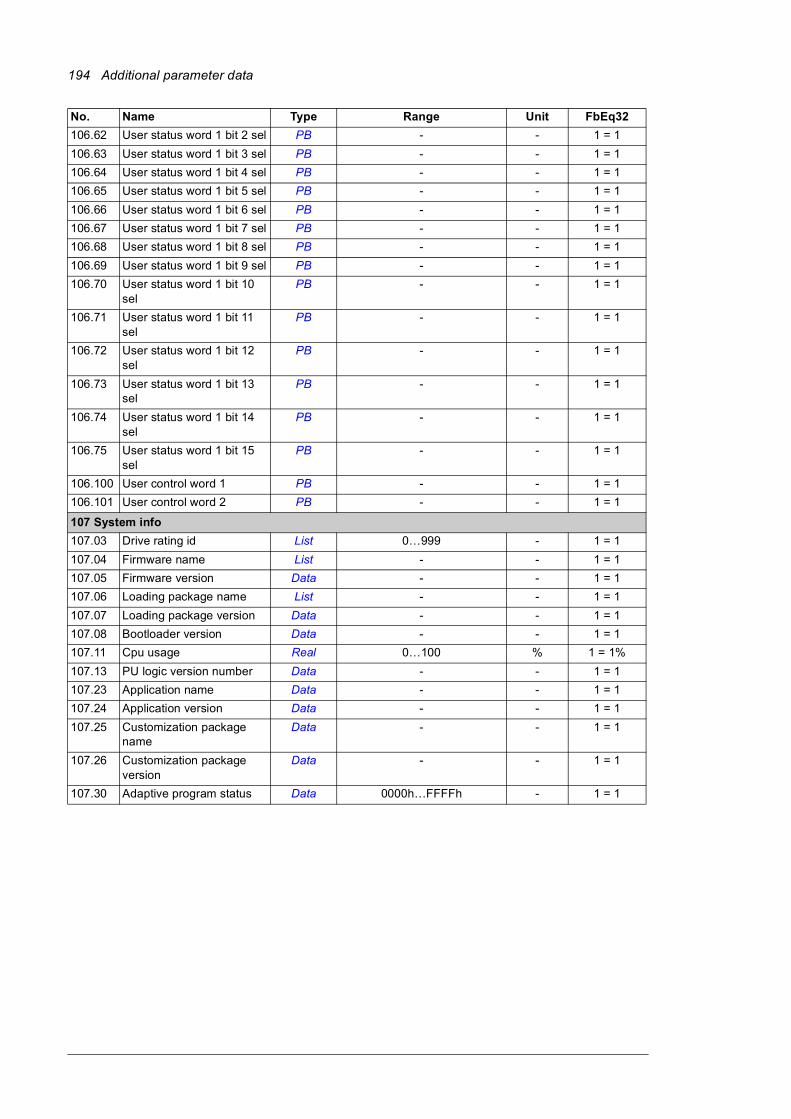
194 Additional parameter data
106.62 User status word 1 bit 2 sel PB - - 1 = 1
106.63 User status word 1 bit 3 sel PB - - 1 = 1
106.64 User status word 1 bit 4 sel PB - - 1 = 1
106.65 User status word 1 bit 5 sel PB - - 1 = 1
106.66 User status word 1 bit 6 sel PB - - 1 = 1
106.67 User status word 1 bit 7 sel PB - - 1 = 1
106.68 User status word 1 bit 8 sel PB - - 1 = 1
106.69 User status word 1 bit 9 sel PB - - 1 = 1
106.70 User status word 1 bit 10 sel
PB - - 1 = 1
106.71 User status word 1 bit 11 sel
PB - - 1 = 1
106.72 User status word 1 bit 12 sel
PB - - 1 = 1
106.73 User status word 1 bit 13 sel
PB - - 1 = 1
106.74 User status word 1 bit 14 sel
PB - - 1 = 1
106.75 User status word 1 bit 15 sel
PB - - 1 = 1
106.100 User control word 1 PB - - 1 = 1
106.101 User control word 2 PB - - 1 = 1
107 System info
107.03 Drive rating id List 0…999 - 1 = 1
107.04 Firmware name List - - 1 = 1
107.05 Firmware version Data - - 1 = 1
107.06 Loading package name List - - 1 = 1
107.07 Loading package version Data - - 1 = 1
107.08 Bootloader version Data - - 1 = 1
107.11 Cpu usage Real 0…100 % 1 = 1%
107.13 PU logic version number Data - - 1 = 1
107.23 Application name Data - - 1 = 1
107.24 Application version Data - - 1 = 1
107.25 Customization package name
Data - - 1 = 1
107.26 Customization package version
Data - - 1 = 1
107.30 Adaptive program status Data 0000h…FFFFh - 1 = 1
No. Name Type Range Unit FbEq32
Additional parameter data 195
Parameter groups 110…209No. Name Type Range Unit FbEq32
110 Standard DI, RO
110.01 DI status PB 0000h…FFFFh - 1 = 1
110.02 DI delayed status PB 0000h…FFFFh - 1 = 1
110.03 DI force selection PB 0000h…FFFFh - 1 = 1
110.04 DI force data PB 0000h…FFFFh - 1 = 1
110.05 DI1 ON delay Real 0.0 … 3000.0 s 10 = 1 s
110.06 DI1 OFF delay Real 0.0 … 3000.0 s 10 = 1 s
110.07 DI2 ON delay Real 0.0 … 3000.0 s 10 = 1 s
110.08 DI2 OFF delay Real 0.0 … 3000.0 s 10 = 1 s
110.09 DI3 ON delay Real 0.0 … 3000.0 s 10 = 1 s
110.10 DI3 OFF delay Real 0.0 … 3000.0 s 10 = 1 s
110.11 DI4 ON delay Real 0.0 … 3000.0 s 10 = 1 s
110.12 DI4 OFF delay Real 0.0 … 3000.0 s 10 = 1 s
110.13 DI5 ON delay Real 0.0 … 3000.0 s 10 = 1 s
110.14 DI5 OFF delay Real 0.0 … 3000.0 s 10 = 1 s
110.15 DI6 ON delay Real 0.0 … 3000.0 s 10 = 1 s
110.16 DI6 OFF delay Real 0.0 … 3000.0 s 10 = 1 s
110.21 RO status PB 0000h…FFFFh - 1 = 1
110.24 RO1 source Binary src - - 1 = 1
110.25 RO1 ON delay Real 0.0 … 3000.0 s 10 = 1 s
110.26 RO1 OFF delay Real 0.0 … 3000.0 s 10 = 1 s
110.27 RO2 source Binary src - - 1 = 1
110.28 RO2 ON delay Real 0.0 … 3000.0 s 10 = 1 s
110.29 RO2 OFF delay Real 0.0 … 3000.0 s 10 = 1 s
110.30 RO3 source Binary src - - 1 = 1
110.31 RO3 ON delay Real 0.0 … 3000.0 s 10 = 1 s
110.32 RO3 OFF delay Real 0.0 … 3000.0 s 10 = 1 s
110.51 DI filter time Real 0.3 … 100.0 ms 10 = 1 ms
110.99 RO/DIO control word PB 0000h…FFFFh - 1 = 1
111 Standard DIO, FI, FO
111.01 DIO status PB 0000h…FFFFh - 1 = 1
111.02 DIO delayed status PB 0000h…FFFFh - 1 = 1
111.05 DIO1 function List 0…2 - 1 = 1
111.06 DIO1 output source Binary src - - 1 = 1
111.07 DIO1 ON delay Real 0.0 … 3000.0 s 10 = 1 s
111.08 DIO1 OFF delay Real 0.0 … 3000.0 s 10 = 1 s
111.09 DIO2 function List 0…1 - 1 = 1
111.10 DIO2 output source Binary src - - 1 = 1
111.11 DIO2 ON delay Real 0.0 … 3000.0 s 10 = 1 s
111.12 DIO2 OFF delay Real 0.0 … 3000.0 s 10 = 1 s
111.38 Freq in 1 actual value Real 0…16000 Hz 1 = 1 Hz
111.39 Freq in 1 scaled Real -32768.000 … 32767.000 - 1000 = 1
111.42 Freq in 1 min Real 0…16000 Hz 1 = 1 Hz
111.43 Freq in 1 max Real 0…16000 Hz 1 = 1 Hz
111.44 Freq in 1 at scaled min Real -32768.000 … 32767.000 - 1000 = 1
111.45 Freq in 1 at scaled max Real -32768.000 … 32767.000 - 1000 = 1
111.81 DIO filter time Real 0.3 … 100.0 ms 10 = 1 ms
196 Additional parameter data
112 Standard AI
112.01 AI tune List 0…4 - 1 = 1
112.03 AI supervision function List 0…2 - 1 = 1
112.04 AI supervision selection PB 0000h…FFFFh - 1 = 1
112.11 AI1 actual value Real -22.000 … 22.000 mA or V 1000 = 1 unit
112.12 AI1 scaled value Real -32768.000 … 32767.000 - 1000 = 1
112.15 AI1 unit selection List 2…10 - 1 = 1
112.16 AI1 filter time Real 0.000 … 30.000 s 1000 = 1 s
112.17 AI1 min Real -22.000 … 22.000 mA or V 1000 = 1 mA or V
112.18 AI1 max Real -22.000 … 22.000 mA or V 1000 = 1 mA or V
112.19 AI1 scaled at AI1 min Real -32768.000 … 32767.000 - 1000 = 1
112.20 AI1 scaled at AI1 max Real -32768.000 … 32767.000 - 1000 = 1
112.21 AI2 actual value Real -22.000 … 22.000 mA or V 1000 = 1 mA or V
112.22 AI2 scaled value Real -32768.000 … 32767.000 - 1000 = 1
112.25 AI2 unit selection List 2…10 - 1 = 1
112.26 AI2 filter time Real 0.000 … 30.000 s 1000 = 1 s
112.27 AI2 min Real -22.000 … 22.000 mA or V 1000 = 1 mA or V
112.28 AI2 max Real -22.000 … 22.000 mA or V 1000 = 1 mA or V
112.29 AI2 scaled at AI2 min Real -32768.000 … 32767.000 - 1000 = 1
112.30 AI2 scaled at AI2 max Real -32768.000 … 32767.000 - 1000 = 1
113 Standard AO
113.11 AO1 actual value Real 0.000 … 22.000 mA 1000 = 1 mA
113.12 AO1 source Analog src - - 1 = 1
113.16 AO1 filter time Real 0.000 … 30.000 s 1000 = 1 s
113.17 AO1 source min Real -32768.0 … 32767.0 - 10 = 1
113.18 AO1 source max Real -32768.0 … 32767.0 - 10 = 1
113.19 AO1 out at AO1 src min Real 0.000 … 22.000 mA 1000 = 1 mA
113.20 AO1 out at AO1 src max Real 0.000 … 22.000 mA 1000 = 1 mA
113.21 AO2 actual value Real 0.000 … 22.000 mA 1000 = 1 mA
113.22 AO2 source Analog src - - 1 = 1
113.26 AO2 filter time Real 0.000 … 30.000 s 1000 = 1 s
113.27 AO2 source min Real -32768.0 … 32767.0 - 10 = 1
113.28 AO2 source max Real -32768.0 … 32767.0 - 10 = 1
113.29 AO2 out at AO2 src min Real 0.000 … 22.000 mA 1000 = 1 mA
113.30 AO2 out at AO2 src max Real 0.000 … 22.000 mA 1000 = 1 mA
113.91 AO1 data storage Real -327.68 … 327.67 - 100 = 1
113.92 AO2 data storage Real -327.68 … 327.67 - 100 = 1
114 Extension I/O module 1
114.01 Module 1 type List 0…4 - 1 = 1
114.02 Module 1 location Real 1…254 - 1 = 1
114.03 Module 1 status List 0…25 - 1 = 1
DIx (114.01 Module 1 type = FDIO-01)
114.05 DI status PB 00000000h…FFFFFFFFh - 1 = 1
114.06 DI delayed status PB 00000000h…FFFFFFFFh - 1 = 1
114.08 DI filter time Real 0.8 … 100.0 ms 10 = 1 ms
114.12 DI1 ON delay Real 0.00 … 3000.00 s 100 = 1 s
114.13 DI1 OFF delay Real 0.00 … 3000.00 s 100 = 1 s
114.17 DI2 ON delay Real 0.00 … 3000.00 s 100 = 1 s
No. Name Type Range Unit FbEq32

Additional parameter data 197
114.18 DI2 OFF delay Real 0.00 … 3000.00 s 100 = 1 s
114.22 DI3 ON delay Real 0.00 … 3000.00 s 100 = 1 s
114.23 DI3 OFF delay Real 0.00 … 3000.00 s 100 = 1 s
Common parameters for DIOx (114.01 Module 1 type = FIO-01 or FIO-11)
114.05 DIO status PB 00000000h…FFFFFFFFh - 1 = 1
114.06 DIO delayed status PB 00000000h…FFFFFFFFh - 1 = 1
DIO1/DIO2 (114.01 Module 1 type = FIO-01 or FIO-11)
114.08 DIO filter time Real 0.8 … 100.0 ms 10 = 1 ms
114.09 DIO1 configuration List 0…1 - 1 = 1
114.11 DIO1 output source Binary src - - 1 = 1
114.12 DIO1 ON delay Real 0.0 … 3000.0 s 10 = 1 s
114.13 DIO1 OFF delay Real 0.0 … 3000.0 s 10 = 1 s
114.14 DIO2 configuration List 0…1 - 1 = 1
114.16 DIO2 output source Binary src - - 1 = 1
114.17 DIO2 ON delay Real 0.0 … 3000.0 s 10 = 1 s
114.18 DIO2 OFF delay Real 0.0 … 3000.0 s 10 = 1 s
DIO3/DIO4 (114.01 Module 1 type = FIO-01)
114.19 DIO3 configuration List 0…1 - 1 = 1
114.21 DIO3 output source Binary src - - 1 = 1
114.22 DIO3 ON delay Real 0.0 … 3000.0 s 10 = 1 s
114.23 DIO3 OFF delay Real 0.0 … 3000.0 s 10 = 1 s
114.24 DIO4 configuration List 0…1 - 1 = 1
114.26 DIO4 output source Binary src - - 1 = 1
114.27 DIO4 ON delay Real 0.0 … 3000.0 s 10 = 1 s
114.28 DIO4 OFF delay Real 0.0 … 3000.0 s 10 = 1 s
RO1/RO2 (114.01 Module 1 type = FIO-01 or FDIO-01)
114.31 RO status PB 0000h…FFFFh - 1 = 1
114.34 RO1 source Binary src - - 1 = 1
114.35 RO1 ON delay Real 0.0 … 3000.0 s 10 = 1 s
114.36 RO1 OFF delay Real 0.0 … 3000.0 s 10 = 1 s
114.37 RO2 source Binary src - - 1 = 1
114.38 RO2 ON delay Real 0.0 … 3000.0 s 10 = 1 s
114.39 RO2 OFF delay Real 0.0 … 3000.0 s 10 = 1 s
Common parameters for AIx (114.01 Module 1 type = FIO-11 or FAIO-01)
114.19 AI supervision function List 0…2 - 1 = 1
114.20 AI supervision selection PB 0000h…FFFFh - 1 = 1
114.22 AI force sel PB 00000000h…FFFFFFFFh - 1 = 1
AI1/AI2 (114.01 Module 1 type = FIO-11 or FAIO-01)
114.26 AI1 actual value Real -22.000 … 22.000 mA or V 1000 = 1 unit
114.27 AI1 scaled value Real -32768.000 … 32767.000 - 1000 = 1
114.28 AI1 force data Real -22.000 … 22.000 mA or V 1000 = 1 unit
114.29 AI1 HW switch pos List - - 1 = 1
114.30 AI1 unit selection List - - 1 = 1
114.31 AI1 filter gain List 0…7 - 1 = 1
114.32 AI1 filter time Real 0.000 … 30.000 s 1000 = 1 s
114.33 AI1 min Real -22.000 … 22.000 mA or V 1000 = 1 mA or V
114.34 AI1 max Real -22.000 … 22.000 mA or V 1000 = 1 mA or V
114.35 AI1 scaled at AI1 min Real -32768.000 … 32767.000 - 1000 = 1
114.36 AI1 scaled at AI1 max Real -32768.000 … 32767.000 - 1000 = 1
No. Name Type Range Unit FbEq32

198 Additional parameter data
114.41 AI2 actual value Real -22.000 … 22.000 mA or V 1000 = 1 unit
114.42 AI2 scaled value Real -32768.000 … 32767.000 - 1000 = 1
114.43 AI2 force data Real -22.000 … 22.000 mA or V 1000 = 1 unit
114.44 AI2 HW switch pos List - - 1 = 1
114.45 AI2 unit selection List - - 1 = 1
114.46 AI2 filter gain List 0…7 - 1 = 1
114.47 AI2 filter time Real 0.000 … 30.000 s 1000 = 1 s
114.48 AI2 min Real -22.000 … 22.000 mA or V 1000 = 1 mA or V
114.49 AI2 max Real -22.000 … 22.000 mA or V 1000 = 1 mA or V
114.50 AI2 scaled at AI2 min Real -32768.000 … 32767.000 - 1000 = 1
114.51 AI2 scaled at AI2 max Real -32768.000 … 32767.000 - 1000 = 1
AI3 (114.01 Module 1 type = FIO-11)
114.56 AI3 actual value Real -22.000 … 22.000 mA or V 1000 = 1 unit
114.57 AI3 scaled value Real -32768.000 … 32767.000 - 1000 = 1
114.58 AI3 force data Real -22.000 … 22.000 mA or V 1000 = 1 unit
114.59 AI3 HW switch pos List - - 1 = 1
114.60 AI3 unit selection List - - 1 = 1
114.61 AI3 filter gain List 0…7 - 1 = 1
114.62 AI3 filter time Real 0.000 … 30.000 s 1000 = 1 s
114.63 AI3 min Real -22.000 … 22.000 mA or V 1000 = 1 mA or V
114.64 AI3 max Real -22.000 … 22.000 mA or V 1000 = 1 mA or V
114.65 AI3 scaled at AI3 min Real -32768.000 … 32767.000 - 1000 = 1
114.66 AI3 scaled at AI3 max Real -32768.000 … 32767.000 - 1000 = 1
Common parameters for AOx (114.01 Module 1 type = FIO-11 or FAIO-01)
114.71 AO force selection PB 00000000h…FFFFFFFFh - 1 = 1
AO1 (114.01 Module 1 type = FIO-11 or FAIO-01)
114.76 AO1 actual value Real 0.000 … 22.000 mA 1000 = 1 mA
114.77 AO1 source Analog src - - 1 = 1
114.78 AO1 force data Real 0.000 … 22.000 mA 1000 = 1 mA
114.79 AO1 filter time Real 0.000 … 30.000 s 1000 = 1 s
114.80 AO1 source min Real -32768.0 … 32767.0 - 10 = 1
114.81 AO1 source max Real -32768.0 … 32767.0 - 10 = 1
114.82 AO1 out at AO1 src min Real 0.000 … 22.000 mA 1000 = 1 mA
114.83 AO1 out at AO1 src max Real 0.000 … 22.000 mA 1000 = 1 mA
AO2 (114.01 Module 1 type = FAIO-01)
114.86 AO2 actual value Real 0.000 … 22.000 mA 1000 = 1 mA
114.87 AO2 source Analog src - - 1 = 1
114.88 AO2 force data Real 0.000 … 22.000 mA 1000 = 1 mA
114.89 AO2 filter time Real 0.000 … 30.000 s 1000 = 1 s
114.90 AO2 source min Real -32768.0 … 32767.0 - 10 = 1
114.91 AO2 source max Real -32768.0 … 32767.0 - 10 = 1
114.92 AO2 out at AO2 src min Real 0.000 … 22.000 mA 1000 = 1 mA
114.93 AO2 out at AO2 src max Real 0.000 … 22.000 mA 1000 = 1 mA
115 Extension I/O module 2
115.01 Module 2 type List 0…4 - 1 = 1
115.02 Module 2 location Real 1…254 - 1 = 1
115.03 Module 2 status List 0…24 - 1 = 1
DIx (115.01 Module 2 type = FDIO-01)
115.05 DI status PB 00000000h…FFFFFFFFh - 1 = 1
No. Name Type Range Unit FbEq32
Additional parameter data 199
115.06 DI delayed status PB 00000000h…FFFFFFFFh - 1 = 1
115.08 DI filter time Real 0.8 … 100.0 ms 10 = 1 ms
115.12 DI1 ON delay Real 0.00 … 3000.00 s 100 = 1 s
115.13 DI1 OFF delay Real 0.00 … 3000.00 s 100 = 1 s
115.17 DI2 ON delay Real 0.00 … 3000.00 s 100 = 1 s
115.18 DI2 OFF delay Real 0.00 … 3000.00 s 100 = 1 s
115.22 DI3 ON delay Real 0.00 … 3000.00 s 100 = 1 s
115.23 DI3 OFF delay Real 0.00 … 3000.00 s 100 = 1 s
Common parameters for DIOx (115.01 Module 2 type = FIO-01 or FIO-11)
115.05 DIO status PB 00000000h…FFFFFFFFh - 1 = 1
115.06 DIO delayed status PB 00000000h…FFFFFFFFh - 1 = 1
DIO1/DIO2 (115.01 Module 2 type = FIO-01 or FIO-11)
115.08 DIO filter time Real 0.8 … 100.0 ms 10 = 1 ms
115.09 DIO1 configuration List 0…1 - 1 = 1
115.11 DIO1 output source Binary src - - 1 = 1
115.12 DIO1 ON delay Real 0.0 … 3000.0 s 10 = 1 s
115.13 DIO1 OFF delay Real 0.0 … 3000.0 s 10 = 1 s
115.14 DIO2 configuration List 0…1 - 1 = 1
115.16 DIO2 output source Binary src - - 1 = 1
115.17 DIO2 ON delay Real 0.0 … 3000.0 s 10 = 1 s
115.18 DIO2 OFF delay Real 0.0 … 3000.0 s 10 = 1 s
DIO3/DIO4 (115.01 Module 2 type = FIO-01)
115.19 DIO3 configuration List 0…1 - 1 = 1
115.21 DIO3 output source Binary src - - 1 = 1
115.22 DIO3 ON delay Real 0.0 … 3000.0 s 10 = 1 s
115.23 DIO3 OFF delay Real 0.0 … 3000.0 s 10 = 1 s
115.24 DIO4 configuration List 0…1 - 1 = 1
115.26 DIO4 output source Binary src - - 1 = 1
115.27 DIO4 ON delay Real 0.0 … 3000.0 s 10 = 1 s
115.28 DIO4 OFF delay Real 0.0 … 3000.0 s 10 = 1 s
RO1/RO2 (115.01 Module 2 type = FIO-01 or FDIO-01)
115.31 RO status PB 0000h…FFFFh - 1 = 1
115.34 RO1 source Binary src - - 1 = 1
115.35 RO1 ON delay Real 0.0 … 3000.0 s 10 = 1 s
115.36 RO1 OFF delay Real 0.0 … 3000.0 s 10 = 1 s
115.37 RO2 source Binary src - - 1 = 1
115.38 RO2 ON delay Real 0.0 … 3000.0 s 10 = 1 s
115.39 RO2 OFF delay Real 0.0 … 3000.0 s 10 = 1 s
Common parameters for AIx (115.01 Module 2 type = FIO-11 or FAIO-01)
115.19 AI supervision function List 0…2 - 1 = 1
115.20 AI supervision selection PB 0000h…FFFFh - 1 = 1
115.22 AI force sel PB 00000000h…FFFFFFFFh - 1 = 1
AI1/AI2 (115.01 Module 2 type = FIO-11 or FAIO-01)
115.26 AI1 actual value Real -22.000 … 22.000 mA or V 1000 = 1 unit
115.27 AI1 scaled value Real -32768.000 … 32767.000 - 1000 = 1
115.28 AI1 force data Real -22.000 … 22.000 mA or V 1000 = 1 unit
115.29 AI1 HW switch pos List - - 1 = 1
115.30 AI1 unit selection List - - 1 = 1
115.31 AI1 filter gain List 0…7 - 1 = 1
No. Name Type Range Unit FbEq32
200 Additional parameter data
115.32 AI1 filter time Real 0.000 … 30.000 s 1000 = 1 s
115.33 AI1 min Real -22.000 … 22.000 mA or V 1000 = 1 mA or V
115.34 AI1 max Real -22.000 … 22.000 mA or V 1000 = 1 mA or V
115.35 AI1 scaled at AI1 min Real -32768.000 … 32767.000 - 1000 = 1
115.36 AI1 scaled at AI1 max Real -32768.000 … 32767.000 - 1000 = 1
115.41 AI2 actual value Real -22.000 … 22.000 mA or V 1000 = 1 unit
115.42 AI2 scaled value Real -32768.000 … 32767.000 - 1000 = 1
115.43 AI2 force data Real -22.000 … 22.000 mA or V 1000 = 1 unit
115.44 AI2 HW switch pos List - - 1 = 1
115.45 AI2 unit selection List - - 1 = 1
115.46 AI2 filter gain List 0…7 - 1 = 1
115.47 AI2 filter time Real 0.000 … 30.000 s 1000 = 1 s
115.48 AI2 min Real -22.000 … 22.000 mA or V 1000 = 1 mA or V
115.49 AI2 max Real -22.000 … 22.000 mA or V 1000 = 1 mA or V
115.50 AI2 scaled at AI2 min Real -32768.000 … 32767.000 - 1000 = 1
115.51 AI2 scaled at AI2 max Real -32768.000 … 32767.000 - 1000 = 1
AI3 (115.01 Module 2 type = FIO-11)
115.56 AI3 actual value Real -22.000 … 22.000 mA or V 1000 = 1 unit
115.57 AI3 scaled value Real -32768.000 … 32767.000 - 1000 = 1
115.58 AI3 force data Real -22.000 … 22.000 mA or V 1000 = 1 unit
115.59 AI3 HW switch pos List - - 1 = 1
115.60 AI3 unit selection List - - 1 = 1
115.61 AI3 filter gain List 0…7 - 1 = 1
115.62 AI3 filter time Real 0.000 … 30.000 s 1000 = 1 s
115.63 AI3 min Real -22.000 … 22.000 mA or V 1000 = 1 mA or V
115.64 AI3 max Real -22.000 … 22.000 mA or V 1000 = 1 mA or V
115.65 AI3 scaled at AI3 min Real -32768.000 … 32767.000 - 1000 = 1
115.66 AI3 scaled at AI3 max Real -32768.000 … 32767.000 - 1000 = 1
Common parameters for AOx (115.01 Module 2 type = FIO-11 or FAIO-01)
115.71 AO force selection PB 00000000h…FFFFFFFFh - 1 = 1
AO1 (115.01 Module 2 type = FIO-11 or FAIO-01)
115.76 AO1 actual value Real 0.000 … 22.000 mA 1000 = 1 mA
115.77 AO1 source Analog src - - 1 = 1
115.78 AO1 force data Real 0.000 … 22.000 mA 1000 = 1 mA
115.79 AO1 filter time Real 0.000 … 30.000 s 1000 = 1 s
115.80 AO1 source min Real -32768.0 … 32767.0 - 10 = 1
115.81 AO1 source max Real -32768.0 … 32767.0 - 10 = 1
115.82 AO1 out at AO1 src min Real 0.000 … 22.000 mA 1000 = 1 mA
115.83 AO1 out at AO1 src max Real 0.000 … 22.000 mA 1000 = 1 mA
AO2 (115.01 Module 2 type = FAIO-01)
115.86 AO2 actual value Real 0.000 … 22.000 mA 1000 = 1 mA
115.87 AO2 source Analog src - - 1 = 1
115.88 AO2 force data Real 0.000 … 22.000 mA 1000 = 1 mA
115.89 AO2 filter time Real 0.000 … 30.000 s 1000 = 1 s
115.90 AO2 source min Real -32768.0 … 32767.0 - 10 = 1
115.91 AO2 source max Real -32768.0 … 32767.0 - 10 = 1
115.92 AO2 out at AO2 src min Real 0.000 … 22.000 mA 1000 = 1 mA
115.93 AO2 out at AO2 src max Real 0.000 … 22.000 mA 1000 = 1 mA
No. Name Type Range Unit FbEq32

Additional parameter data 201
116 Extension I/O module 3
116.01 Module 3 type List 0…4 - 1 = 1
116.02 Module 3 location Real 1…254 - 1 = 1
116.03 Module 3 status List 0…24 - 1 = 1
DIx (116.01 Module 3 type = FDIO-01)
116.05 DI status PB 00000000h…FFFFFFFFh - 1 = 1
116.06 DI delayed status PB 00000000h…FFFFFFFFh - 1 = 1
116.08 DI filter time Real 0.8 … 100.0 ms 10 = 1 ms
116.12 DI1 ON delay Real 0.00 … 3000.00 s 100 = 1 s
116.13 DI1 OFF delay Real 0.00 … 3000.00 s 100 = 1 s
116.17 DI2 ON delay Real 0.00 … 3000.00 s 100 = 1 s
116.18 DI2 OFF delay Real 0.00 … 3000.00 s 100 = 1 s
116.22 DI3 ON delay Real 0.00 … 3000.00 s 100 = 1 s
116.23 DI3 OFF delay Real 0.00 … 3000.00 s 100 = 1 s
Common parameters for DIOx (116.01 Module 3 type = FIO-01 or FIO-11)
116.05 DIO status PB 00000000h…FFFFFFFFh - 1 = 1
116.06 DIO delayed status PB 00000000h…FFFFFFFFh - 1 = 1
DIO1/DIO2 (116.01 Module 3 type = FIO-01 or FIO-11)
116.08 DIO filter time Real 0.8 … 100.0 ms 10 = 1 ms
116.09 DIO1 configuration List 0…1 - 1 = 1
116.11 DIO1 output source Binary src - - 1 = 1
116.12 DIO1 ON delay Real 0.0 … 3000.0 s 10 = 1 s
116.13 DIO1 OFF delay Real 0.0 … 3000.0 s 10 = 1 s
116.14 DIO2 configuration List 0…1 - 1 = 1
116.16 DIO2 output source Binary src - - 1 = 1
116.17 DIO2 ON delay Real 0.0 … 3000.0 s 10 = 1 s
116.18 DIO2 OFF delay Real 0.0 … 3000.0 s 10 = 1 s
DIO3/DIO4 (116.01 Module 3 type = FIO-01)
116.19 DIO3 configuration List 0…1 - 1 = 1
116.21 DIO3 output source Binary src - - 1 = 1
116.22 DIO3 ON delay Real 0.0 … 3000.0 s 10 = 1 s
116.23 DIO3 OFF delay Real 0.0 … 3000.0 s 10 = 1 s
116.24 DIO4 configuration List 0…1 - 1 = 1
116.26 DIO4 output source Binary src - - 1 = 1
116.27 DIO4 ON delay Real 0.0 … 3000.0 s 10 = 1 s
116.28 DIO4 OFF delay Real 0.0 … 3000.0 s 10 = 1 s
RO1/RO2 (116.01 Module 3 type = FIO-01 or FDIO-01)
116.31 RO status PB 0000h…FFFFh - 1 = 1
116.34 RO1 source Binary src - - 1 = 1
116.35 RO1 ON delay Real 0.0 … 3000.0 s 10 = 1 s
116.36 RO1 OFF delay Real 0.0 … 3000.0 s 10 = 1 s
116.37 RO2 source Binary src - - 1 = 1
116.38 RO2 ON delay Real 0.0 … 3000.0 s 10 = 1 s
116.39 RO2 OFF delay Real 0.0 … 3000.0 s 10 = 1 s
Common parameters for AIx (116.01 Module 3 type = FIO-11 or FAIO-01)
116.19 AI supervision function List 0…2 - 1 = 1
116.20 AI supervision selection PB 0000h…FFFFh - 1 = 1
116.22 AI force sel PB 00000000h…FFFFFFFFh - 1 = 1
No. Name Type Range Unit FbEq32

202 Additional parameter data
AI1/AI2 (116.01 Module 3 type = FIO-11 or FAIO-01)
116.26 AI1 actual value Real -22.000 … 22.000 mA or V 1000 = 1 unit
116.27 AI1 scaled value Real -32768.000 … 32767.000 - 1000 = 1
116.28 AI1 force data Real -22.000 … 22.000 mA or V 1000 = 1 unit
116.29 AI1 HW switch pos List - - 1 = 1
116.30 AI1 unit selection List - - 1 = 1
116.31 AI1 filter gain List 0…7 - 1 = 1
116.32 AI1 filter time Real 0.000 … 30.000 s 1000 = 1 s
116.33 AI1 min Real -22.000 … 22.000 mA or V 1000 = 1 mA or V
116.34 AI1 max Real -22.000 … 22.000 mA or V 1000 = 1 mA or V
116.35 AI1 scaled at AI1 min Real -32768.000 … 32767.000 - 1000 = 1
116.36 AI1 scaled at AI1 max Real -32768.000 … 32767.000 - 1000 = 1
116.41 AI2 actual value Real -22.000 … 22.000 mA or V 1000 = 1 unit
116.42 AI2 scaled value Real -32768.000 … 32767.000 - 1000 = 1
116.43 AI2 force data Real -22.000 … 22.000 mA or V 1000 = 1 unit
116.44 AI2 HW switch pos List - - 1 = 1
116.45 AI2 unit selection List - - 1 = 1
116.46 AI2 filter gain List 0…7 - 1 = 1
116.47 AI2 filter time Real 0.000 … 30.000 s 1000 = 1 s
116.48 AI2 min Real -22.000 … 22.000 mA or V 1000 = 1 mA or V
116.49 AI2 max Real -22.000 … 22.000 mA or V 1000 = 1 mA or V
116.50 AI2 scaled at AI2 min Real -32768.000 … 32767.000 - 1000 = 1
116.51 AI2 scaled at AI2 max Real -32768.000 … 32767.000 - 1000 = 1
AI3 (116.01 Module 3 type = FIO-11)
116.56 AI3 actual value Real -22.000 … 22.000 mA or V 1000 = 1 unit
116.57 AI3 scaled value Real -32768.000 … 32767.000 - 1000 = 1
116.58 AI3 force data Real -22.000 … 22.000 mA or V 1000 = 1 unit
116.59 AI3 HW switch pos List - - 1 = 1
116.60 AI3 unit selection List - - 1 = 1
116.61 AI3 filter gain List 0…7 - 1 = 1
116.62 AI3 filter time Real 0.000 … 30.000 s 1000 = 1 s
116.63 AI3 min Real -22.000 … 22.000 mA or V 1000 = 1 mA or V
116.64 AI3 max Real -22.000 … 22.000 mA or V 1000 = 1 mA or V
116.65 AI3 scaled at AI3 min Real -32768.000 … 32767.000 - 1000 = 1
116.66 AI3 scaled at AI3 max Real -32768.000 … 32767.000 - 1000 = 1
Common parameters for AOx (116.01 Module 3 type = FIO-11 or FAIO-01)
116.71 AO force selection PB 00000000h…FFFFFFFFh - 1 = 1
AO1 (116.01 Module 3 type = FIO-11 or FAIO-01)
116.76 AO1 actual value Real 0.000 … 22.000 mA 1000 = 1 mA
116.77 AO1 source Analog src - - 1 = 1
116.78 AO1 force data Real 0.000 … 22.000 mA 1000 = 1 mA
116.79 AO1 filter time Real 0.000 … 30.000 s 1000 = 1 s
116.80 AO1 source min Real -32768.0 … 32767.0 - 10 = 1
116.81 AO1 source max Real -32768.0 … 32767.0 - 10 = 1
116.82 AO1 out at AO1 src min Real 0.000 … 22.000 mA 1000 = 1 mA
116.83 AO1 out at AO1 src max Real 0.000 … 22.000 mA 1000 = 1 mA
AO2 (116.01 Module 3 type = FAIO-01)
116.86 AO2 actual value Real 0.000 … 22.000 mA 1000 = 1 mA
116.87 AO2 source Analog src - - 1 = 1
No. Name Type Range Unit FbEq32

Additional parameter data 203
116.88 AO2 force data Real 0.000 … 22.000 mA 1000 = 1 mA
116.89 AO2 filter time Real 0.000 … 30.000 s 1000 = 1 s
116.90 AO2 source min Real -32768.0 … 32767.0 - 10 = 1
116.91 AO2 source max Real -32768.0 … 32767.0 - 10 = 1
116.92 AO2 out at AO2 src min Real 0.000 … 22.000 mA 1000 = 1 mA
116.93 AO2 out at AO2 src max Real 0.000 … 22.000 mA 1000 = 1 mA
119 Operation mode
119.01 Actual operation mode List 1…3 - 1 = 1
119.11 Ext1/Ext2 selection Binary src - - 1 = 1
119.12 Ext1 ctrl mode1 List 1…3 - 1 = 1
119.14 Ext2 ctrl mode1 List 1…3 - 1 = 1
119.16 Local ctrl mode List 1…3 - 1 = 1
119.17 Local control disable List 0…1 - 1 = 1
120 Start/stop
120.01 Ext1 commands List 0…22 - 1 = 1
120.02 Ext1 start trigger type List 0…1 - 1 = 1
120.03 Ext1 in1 source Binary src - - 1 = 1
120.04 Ext1 in2 source Binary src - - 1 = 1
120.06 Ext2 commands List - - 1 = 1
120.07 Ext2 start trigger type List 0…1 - 1 = 1
120.08 Ext2 in1 source Binary src - - 1 = 1
120.09 Ext2 in2 source Binary src - - 1 = 1
120.12 Run enable 1 source Binary src - - 1 = 1
120.19 Enable start command Binary src - - 1 = 1
120.21 Delay for MCB DI3 supervision
Real 0.00…8.00 s 100 = 1 s
120.22 Max current for MCB closing
Real 0…10 % 1 = 1%
120.23 Max DC charging time Real 0.00…10.00 s 100 = 1 s
120.25 MCB closing level Real 20…100 % 1 = 1%
120.26 Maximum dU/dt Real 0.0…200.0 V/s 1 = 1 V/s
120.27 Start delay Real 0.00…10.00 s 100 = 1 s
120.28 MCB relay timing Real -6.00…6.00 s 100 = 1 s
120.29 Diode mode Binary src - - 1 = 1
120.30 External charge enable List 0…1 - 1 = 1
120.50 Charging overload event sel
List 0…2 - 1 = 1
121 Start/stop mode
121.04 Emergency stop mode List 0…2 - 1 = 1
121.05 Emergency stop source Binary src - - 1 = 1
122 Power reference
122.01 User Power ref Real - - 100 = 1
122.02 Power ref sel List - - 1 = 1
122.03 Power ref 1 Real - - 1 = 1
122.04 Power ref scale Real -1000.00 …1000.00 - 100 = 1
122.05 Power ref 2 Real - - 100 = 1
122.06 Power ref type List 0…3 - 1 = 1
122.07 Ipower ref % Real -1000.0 …1000.0 % 10 = 1%
122.08 Ipower ref Real - A 100 = 1 A
No. Name Type Range Unit FbEq32
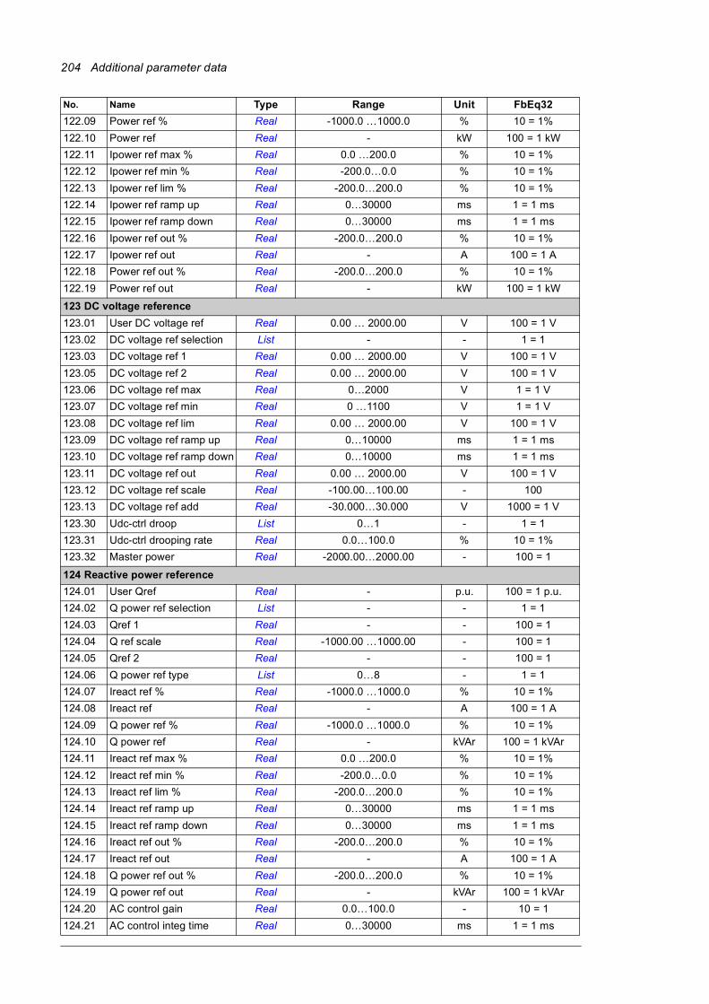
204 Additional parameter data
122.09 Power ref % Real -1000.0 …1000.0 % 10 = 1%
122.10 Power ref Real - kW 100 = 1 kW
122.11 Ipower ref max % Real 0.0 …200.0 % 10 = 1%
122.12 Ipower ref min % Real -200.0…0.0 % 10 = 1%
122.13 Ipower ref lim % Real -200.0…200.0 % 10 = 1%
122.14 Ipower ref ramp up Real 0…30000 ms 1 = 1 ms
122.15 Ipower ref ramp down Real 0…30000 ms 1 = 1 ms
122.16 Ipower ref out % Real -200.0…200.0 % 10 = 1%
122.17 Ipower ref out Real - A 100 = 1 A
122.18 Power ref out % Real -200.0…200.0 % 10 = 1%
122.19 Power ref out Real - kW 100 = 1 kW
123 DC voltage reference
123.01 User DC voltage ref Real 0.00 … 2000.00 V 100 = 1 V
123.02 DC voltage ref selection List - - 1 = 1
123.03 DC voltage ref 1 Real 0.00 … 2000.00 V 100 = 1 V
123.05 DC voltage ref 2 Real 0.00 … 2000.00 V 100 = 1 V
123.06 DC voltage ref max Real 0…2000 V 1 = 1 V
123.07 DC voltage ref min Real 0 …1100 V 1 = 1 V
123.08 DC voltage ref lim Real 0.00 … 2000.00 V 100 = 1 V
123.09 DC voltage ref ramp up Real 0…10000 ms 1 = 1 ms
123.10 DC voltage ref ramp down Real 0…10000 ms 1 = 1 ms
123.11 DC voltage ref out Real 0.00 … 2000.00 V 100 = 1 V
123.12 DC voltage ref scale Real -100.00…100.00 - 100
123.13 DC voltage ref add Real -30.000…30.000 V 1000 = 1 V
123.30 Udc-ctrl droop List 0…1 - 1 = 1
123.31 Udc-ctrl drooping rate Real 0.0…100.0 % 10 = 1%
123.32 Master power Real -2000.00…2000.00 - 100 = 1
124 Reactive power reference
124.01 User Qref Real - p.u. 100 = 1 p.u.
124.02 Q power ref selection List - - 1 = 1
124.03 Qref 1 Real - - 100 = 1
124.04 Q ref scale Real -1000.00 …1000.00 - 100 = 1
124.05 Qref 2 Real - - 100 = 1
124.06 Q power ref type List 0…8 - 1 = 1
124.07 Ireact ref % Real -1000.0 …1000.0 % 10 = 1%
124.08 Ireact ref Real - A 100 = 1 A
124.09 Q power ref % Real -1000.0 …1000.0 % 10 = 1%
124.10 Q power ref Real - kVAr 100 = 1 kVAr
124.11 Ireact ref max % Real 0.0 …200.0 % 10 = 1%
124.12 Ireact ref min % Real -200.0…0.0 % 10 = 1%
124.13 Ireact ref lim % Real -200.0…200.0 % 10 = 1%
124.14 Ireact ref ramp up Real 0…30000 ms 1 = 1 ms
124.15 Ireact ref ramp down Real 0…30000 ms 1 = 1 ms
124.16 Ireact ref out % Real -200.0…200.0 % 10 = 1%
124.17 Ireact ref out Real - A 100 = 1 A
124.18 Q power ref out % Real -200.0…200.0 % 10 = 1%
124.19 Q power ref out Real - kVAr 100 = 1 kVAr
124.20 AC control gain Real 0.0…100.0 - 10 = 1
124.21 AC control integ time Real 0…30000 ms 1 = 1 ms
No. Name Type Range Unit FbEq32

Additional parameter data 205
124.22 AC diff max % Real 0.0…30.0 % 10 = 1%
124.23 AC diff min % Real -30.0…0.0 % 10 = 1%
124.27 AC control base grid voltage
Real 100…1000 V 1 = 1 V
124.30 Q(x) input signal List 0…2 - 1 = 1
124.31 Lock-in level Real 0.0…200.0 % 10 = 1%
124.32 Lock-out level Real 0.0…200.0 % 10 = 1%
124.33 Q(x) input level 1 Real - % 10 = 1%
124.34 Q(x) input level 2 Real - % 10 = 1%
124.35 Q(x) input level 3 Real - % 10 = 1%
124.36 Q(x) input level 4 Real - % 10 = 1%
124.37 Q(x) input level 5 Real - % 10 = 1%
124.38 Q(x) input level 6 Real - % 10 = 1%
124.39 Q(x) output level 1 Real - - 100 = 1
124.40 Q(x) output level 2 Real - - 100 = 1
124.41 Q(x) output level 3 Real - - 100 = 1
124.42 Q(x) output level 4 Real - - 100 = 1
124.43 Q(x) output level 5 Real - - 100 = 1
124.44 Q(x) output level 6 Real - - 100 = 1
130 Limits
130.01 Limit word 1 PB 0000h…FFFFh - 1 = 1
130.02 Limit word 2 PB 0000h…FFFFh - 1 = 1
130.03 Limit word 3 PB 0000h…FFFFh - 1 = 1
130.04 Limit word 4 PB 0000h…FFFFh - 1 = 1
130.16 Q cooling overtemp limit List 0…1 - 1 = 1
130.17 Q cooling temp 1 Real 0.00 … 200.00 °C 100 = 1 °C
130.18 Q cooling temp 2 Real 0.00 … 200.00 °C 100 = 1 °C
130.19 Q cooling temp 3 Real 0.00 … 200.00 °C 100 = 1 °C
130.20 Q cooling limit level 2 Real 0 … 100 % 1 = 1%
130.21 Q cooling limit level 3 Real 0 … 100 % 1 = 1%
130.22 Q power unit overtemp limit
List 0…1 - 1 = 1
130.23 Q power unit temp 1 Real 0.0 … 100.0 % 10 = 1%
130.24 Q power unit temp 2 Real 0.0 … 100.0 % 10 = 1%
130.25 Q power unit limit level Real 0 … 100 % 1 = 1%
130.30 Ireact limit % Real -200.0 … 200.0 % 10 = 1%
130.31 Ireact limit Real - A 100 = 1 A
130.32 Q power limit % Real -200.0 … 200.0 % 10 = 1%
130.33 Q power limit Real - kVAr 100 = 1 kVAr
130.46 Current limit % Real 0…200 % 1 = 1%
130.47 Power sign change List 0…1 - 1 = 1
130.48 User power limit max % Real 0.0…200.0 % 10 = 1%
130.49 User power limit min % Real -200.0…0.0 % 10 = 1%
130.50 Ext Tmp1 input selection List - - 1 = 1
130.51 Ext Tmp2 input selection List - - 1 = 1
130.52 Ext Tmp1 Real - °C 100 = 1 °C
130.53 Ext Tmp2 Real - °C 100 = 1 °C
130.54 Pt current Real 0.0…10.0 mA 10 = 1 mA
130.55 Cyclic Pt current Real - mA 10 = 1 mA
No. Name Type Range Unit FbEq32

206 Additional parameter data
130.58 Cooling temp source List 0…2 - 1 = 1
130.83 User DC voltage min limit Real 0…2500 V 1 = 1 V
130.84 User DC voltage max limit Real 0…2500 V 1 = 1 V
131 Fault functions
131.01 External event 1 source Binary src - - 1 = 1
131.02 External event 1 type List 0…3 - 1 = 1
131.03 External event 2 source Binary src - - 1 = 1
131.04 External event 2 type List 0…1 - 1 = 1
131.05 External event 3 source Binary src - - 1 = 1
131.06 External event 3 type List 0…1 - 1 = 1
131.07 External event 4 source Binary src - - 1 = 1
131.08 External event 4 type List 0…1 - 1 = 1
131.09 External event 5 source Binary src - - 1 = 1
131.10 External event 5 type List 0…1 - 1 = 1
131.11 Fault reset selection Binary src - - 1 = 1
131.12 Autoreset selection PB 0000h…FFFFh - 1 = 1
131.13 User selectable fault Real 0…65535 - 1 = 1
131.14 Number of trials Real 0…5 - 1 = 1
131.15 Total trials time Real 1.0 … 600.0 s 10 = 1 s
131.16 Delay time Real 0.0 … 120.0 s 10 = 1 s
131.20 Earth fault List 0…2 - 1 = 1
131.28 Ext earth leakage signal source
Binary src - - 1 = 1
131.29 Ext earth leakage action List 0…1 - 1 = 1
131.32 Aux circuit breaker fault source
Binary src - - 1 = 1
131.33 Cabinet temperature fault source
Binary src - - 1 = 1
131.34 Cabinet temperature supervision
List 0…1 - 1 = 1
131.35 Main fan fault function List 0…2 - 1 = 1
131.38 Fuse trip fault source Binary src - - 1 = 1
131.39 Brake chopper fault source
Binary src - - 1 = 1
131.40 Disable warning messages
PB 0000h…FFFFh - 1 = 1
133 Generic timer & counter
133.01 Counter status PB 000000b…111111b - 1 = 1
133.10 On-time 1 actual Real 0…4294967295 s 1 = 1 s
133.11 On-time 1 limit Real 0…4294967295 s 1 = 1 s
133.12 On-time 1 function PB 00b…11b - 1 = 1
133.13 On-time 1 source Binary src - - 1 = 1
133.14 On-time 1 warning select List - - 1 = 1
133.20 On-time 2 actual Real 0…4294967295 s 1 = 1 s
133.21 On-time 2 limit Real 0…4294967295 s 1 = 1 s
133.22 On-time 2 function PB 00b…11b - 1 = 1
133.23 On-time 2 source Binary src - - 1 = 1
133.24 On-time 2 warning select List - - 1 = 1
133.30 Edge counter 1 actual Real 0…4294967295 - 1 = 1
133.31 Edge counter 1 limit Real 0…4294967295 - 1 = 1
No. Name Type Range Unit FbEq32

Additional parameter data 207
133.32 Edge counter 1 func PB 0000b…1111b - 1 = 1
133.33 Edge counter 1 source Binary src - - 1 = 1
133.34 Edge counter 1 divider Real 1…4294967295 - 1 = 1
133.35 Edge counter 1 warning selection
List - - 1 = 1
133.40 Edge counter 2 actual Real 0…4294967295 - 1 = 1
133.41 Edge counter 2 limit Real 0…4294967295 - 1 = 1
133.42 Edge counter 2 function PB 0000b…1111b - 1 = 1
133.43 Edge counter 2 source Binary src - - 1 = 1
133.44 Edge counter 2 divider Real 1…4294967295 - 1 = 1
133.45 Edge counter 2 warning selection
List - - 1 = 1
133.50 Value counter 1 actual Real -2147483008 … 2147483008 - 1 = 1
133.51 Value counter 1 limit Real -2147483008 … 2147483008 - 1 = 1
133.52 Value counter 1 function PB 00b…11b - 1 = 1
133.53 Value counter 1 source Analog src - - 1 = 1
133.54 Value counter 1 divider Real 0.001 … 2147483.647 - 1000 = 1
133.55 Value counter 1 warning select
List - - 1 = 1
133.60 Value counter 2 actual Real -2147483008 … 2147483008 - 1 = 1
133.61 Value counter 2 limit Real -2147483008 … 2147483008 - 1 = 1
133.62 Value counter 2 function PB 00b…11b - 1 = 1
133.63 Value counter 2 source Analog src - - 1 = 1
133.64 Value counter 2 divider Real 0.001 … 2147483.647 - 1000 = 1
133.65 Value counter 2 warning selection
List - - 1 = 1
136 Load analyzer
136.01 PVL signal source Analog src - - 1 = 1
136.02 PVL filter time Real 0.00 … 120.00 s 100 = 1 s
136.06 AL2 signal source Analog src - - 1 = 1
136.07 AL2 signal scaling Real 0.00 … 32767.00 - 100 = 1
136.09 Reset loggers List 0…3 - 1 = 1
136.10 PVL peak value Real -32768.00 … 32767.00 - 100 = 1
136.11 PVL peak date Data - - 1 = 1
136.12 PVL peak time Data - - 1 = 1
136.13 PVL current at peak Real -32768.00 … 32767.00 A 100 = 1 A
136.14 PVL DC voltage at peak Real 0.00 … 2000.00 V 100 = 1 V
136.15 PVL power at peak Real -32768.00 … 32767.00 kW 100 = 1 kW
136.16 PVL reset date Data - - 1 = 1
136.17 PVL reset time Data - - 1 = 1
136.20 AL1 below 10% Real 0.00 … 100.00 % 100 = 1%
136.21 AL1 10 to 20% Real 0.00 … 100.00 % 100 = 1%
136.22 AL1 20 to 30% Real 0.00 … 100.00 % 100 = 1%
136.23 AL1 30 to 40% Real 0.00 … 100.00 % 100 = 1%
136.24 AL1 40 to 50% Real 0.00 … 100.00 % 100 = 1%
136.25 AL1 50 to 60% Real 0.00 … 100.00 % 100 = 1%
136.26 AL1 60 to 70% Real 0.00 … 100.00 % 100 = 1%
136.27 AL1 70 to 80% Real 0.00 … 100.00 % 100 = 1%
136.28 AL1 80 to 90% Real 0.00 … 100.00 % 100 = 1%
No. Name Type Range Unit FbEq32
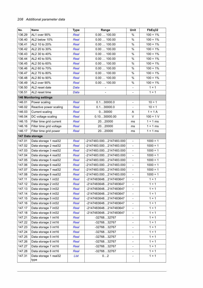
208 Additional parameter data
136.29 AL1 over 90% Real 0.00 … 100.00 % 100 = 1%
136.40 AL2 below 10% Real 0.00 … 100.00 % 100 = 1%
136.41 AL2 10 to 20% Real 0.00 … 100.00 % 100 = 1%
136.42 AL2 20 to 30% Real 0.00 … 100.00 % 100 = 1%
136.43 AL2 30 to 40% Real 0.00 … 100.00 % 100 = 1%
136.44 AL2 40 to 50% Real 0.00 … 100.00 % 100 = 1%
136.45 AL2 50 to 60% Real 0.00 … 100.00 % 100 = 1%
136.46 AL2 60 to 70% Real 0.00 … 100.00 % 100 = 1%
136.47 AL2 70 to 80% Real 0.00 … 100.00 % 100 = 1%
136.48 AL2 80 to 90% Real 0.00 … 100.00 % 100 = 1%
136.49 AL2 over 90% Real 0.00 … 100.00 % 100 = 1%
136.50 AL2 reset date Data - - 1 = 1
136.51 AL2 reset time Data - - 1 = 1
146 Monitoring settings
146.01 Power scaling Real 0.1…30000.0 - 10 = 1
146.02 Reactive power scaling Real 0.1…30000.0 - 10 = 1
146.03 Current scaling Real 0…30000 A 1 = 1 A
146.04 DC voltage scaling Real 0.10…30000.00 V 100 = 1 V
146.15 Filter time grid current Real 20…20000 ms 1 = 1 ms
146.16 Filter time grid voltage Real 20…20000 ms 1 = 1 ms
146.17 Filter time grid power Real 20…20000 ms 1 = 1 ms
147 Data storage
147.01 Data storage 1 real32 Real -2147483.000…2147483.000 - 1000 = 1
147.02 Data storage 2 real32 Real -2147483.000…2147483.000 - 1000 = 1
147.03 Data storage 3 real32 Real -2147483.000…2147483.000 - 1000 = 1
147.04 Data storage 4 real32 Real -2147483.000…2147483.000 - 1000 = 1
147.05 Data storage 5 real32 Real -2147483.000…2147483.000 - 1000 = 1
147.06 Data storage 6 real32 Real -2147483.000…2147483.000 - 1000 = 1
147.07 Data storage 7 real32 Real -2147483.000…2147483.000 - 1000 = 1
147.08 Data storage 8 real32 Real -2147483.000…2147483.000 - 1000 = 1
147.11 Data storage 1 int32 Real -2147483648…2147483647 - 1 = 1
147.12 Data storage 2 int32 Real -2147483648…2147483647 - 1 = 1
147.13 Data storage 3 int32 Real -2147483648…2147483647 - 1 = 1
147.14 Data storage 4 int32 Real -2147483648…2147483647 - 1 = 1
147.15 Data storage 5 int32 Real -2147483648…2147483647 - 1 = 1
147.16 Data storage 6 int32 Real -2147483648…2147483647 - 1 = 1
147.17 Data storage 7 int32 Real -2147483648…2147483647 - 1 = 1
147.18 Data storage 8 int32 Real -2147483648…2147483647 - 1 = 1
147.21 Data storage 1 int16 Real -32768…32767 - 1 = 1
147.22 Data storage 2 int16 Real -32768…32767 - 1 = 1
147.23 Data storage 3 int16 Real -32768…32767 - 1 = 1
147.24 Data storage 4 int16 Real -32768…32767 - 1 = 1
147.25 Data storage 5 int16 Real -32768…32767 - 1 = 1
147.26 Data storage 6 int16 Real -32768…32767 - 1 = 1
147.27 Data storage 7 int16 Real -32768…32767 - 1 = 1
147.28 Data storage 8 int16 Real -32768…32767 - 1 = 1
147.31 Data storage 1 real32 type
List 0…2 - 1 = 1
No. Name Type Range Unit FbEq32
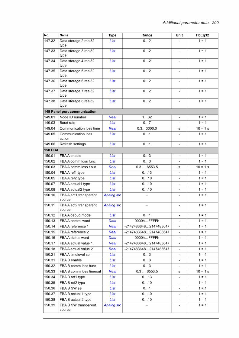
Additional parameter data 209
147.32 Data storage 2 real32 type
List 0…2 - 1 = 1
147.33 Data storage 3 real32 type
List 0…2 - 1 = 1
147.34 Data storage 4 real32 type
List 0…2 - 1 = 1
147.35 Data storage 5 real32 type
List 0…2 - 1 = 1
147.36 Data storage 6 real32 type
List 0…2 - 1 = 1
147.37 Data storage 7 real32 type
List 0…2 - 1 = 1
147.38 Data storage 8 real32 type
List 0…2 - 1 = 1
149 Panel port communication
149.01 Node ID number Real 1…32 - 1 = 1
149.03 Baud rate List 0…7 - 1 = 1
149.04 Communication loss time Real 0.3…3000.0 s 10 = 1 s
149.05 Communication loss action
List 0…1 - 1 = 1
149.06 Refresh settings List 0…1 - 1 = 1
150 FBA
150.01 FBA A enable List 0…3 - 1 = 1
150.02 FBA A comm loss func List 0…3 - 1 = 1
150.03 FBA A comm loss t out Real 0.3 … 6553.5 s 10 = 1 s
150.04 FBA A ref1 type List 0…13 - 1 = 1
150.05 FBA A ref2 type List 0…10 - 1 = 1
150.07 FBA A actual1 type List 0…10 - 1 = 1
150.08 FBA A actual2 type List 0…10 - 1 = 1
150.10 FBA A act1 transparent source
Analog src - - 1 = 1
150.11 FBA A act2 transparent source
Analog src - - 1 = 1
150.12 FBA A debug mode List 0…1 - 1 = 1
150.13 FBA A control word Data 0000h…FFFFh - 1 = 1
150.14 FBA A reference 1 Real -2147483648…2147483647 - 1 = 1
150.15 FBA A reference 2 Real -2147483648…2147483647 - 1 = 1
150.16 FBA A status word Data 0000h…FFFFh - 1 = 1
150.17 FBA A actual value 1 Real -2147483648…2147483647 - 1 = 1
150.18 FBA A actual value 2 Real -2147483648…2147483647 - 1 = 1
150.21 FBA A timelevel sel List 0…3 - 1 = 1
150.31 FBA B enable List 0…3 - 1 = 1
150.32 FBA B comm loss func List 0…3 - 1 = 1
150.33 FBA B comm loss timeout Real 0.3 … 6553.5 s 10 = 1 s
150.34 FBA B ref1 type List 0…13 - 1 = 1
150.35 FBA B ref2 type List 0…10 - 1 = 1
150.36 FBA B SW sel List 0…1 - 1 = 1
150.37 FBA B actual 1 type List 0…10 - 1 = 1
150.38 FBA B actual 2 type List 0…10 - 1 = 1
150.39 FBA B SW transparent source
Analog src - - 1 = 1
No. Name Type Range Unit FbEq32

210 Additional parameter data
150.40 FBA B act1 transparent source
Analog src - - 1 = 1
150.41 FBA B act2 transparent source
Analog src - - 1 = 1
150.42 FBA B debug mode Data 0…1 - 1 = 1
150.43 FBA B control word Real 00000000h … FFFFFFFFh - 1 = 1
150.44 FBA B reference 1 Real -2147483648…2147483647 - 1 = 1
150.45 FBA B reference 2 Real -2147483648…2147483647 - 1 = 1
150.46 FBA B status word Data 00000000h … FFFFFFFFh - 1 = 1
150.47 FBA B actual value 1 Real -2147483648…2147483647 - 1 = 1
150.48 FBA B actual value 2 Real -2147483648…2147483647 - 1 = 1
150.51 FBA B timelevel sel List 0…3 - 1 = 1
151 FBA A settings
151.01 FBA A type List - - 1 = 1
151.02 FBA A Par2 Real 0…65535 - 1 = 1
… … … … …
151.26 FBA A Par26 Real 0…65535 - 1 = 1
151.27 FBA A par refresh List 0…1 - 1 = 1
151.28 FBA A par table ver Data - - 1 = 1
151.29 FBA A drive type code Real 0…65535 - 1 = 1
151.30 FBA A mapping file ver Real 0…65535 - 1 = 1
151.31 D2FBA A comm status List 0…6 - 1 = 1
151.32 FBA A comm SW ver Data - - 1 = 1
151.33 FBA A appl SW ver Data - - 1 = 1
152 FBA A data in
152.01 FBA A data in1 List - - 1 = 1
… … … … …
152.12 FBA A data in12 List - - 1 = 1
153 FBA A data out
153.01 FBA data out1 List - - 1 = 1
… … … … …
153.12 FBA data out12 List - - 1 = 1
154 FBA B settings
154.01 FBA B type List - - 1 = 1
154.02 FBA B Par2 Real 0…65535 - 1 = 1
… … … … …
154.26 FBA B Par26 Real 0…65535 - 1 = 1
154.27 FBA B par refresh List 0…1 - 1 = 1
154.28 FBA B par table ver Data - - 1 = 1
154.29 FBA B drive type code Real 0…65535 - 1 = 1
154.30 FBA B mapping file ver Real 0…65535 - 1 = 1
154.31 D2FBA B comm sta List 0…6 - 1 = 1
154.32 FBA B comm SW ver Data - - 1 = 1
154.33 FBA B appl SW ver Data - - 1 = 1
155 FBA B data in
155.01 FBA B data in1 List - - 1 = 1
… … … … …
155.12 FBA B data in12 List - - 1 = 1
No. Name Type Range Unit FbEq32
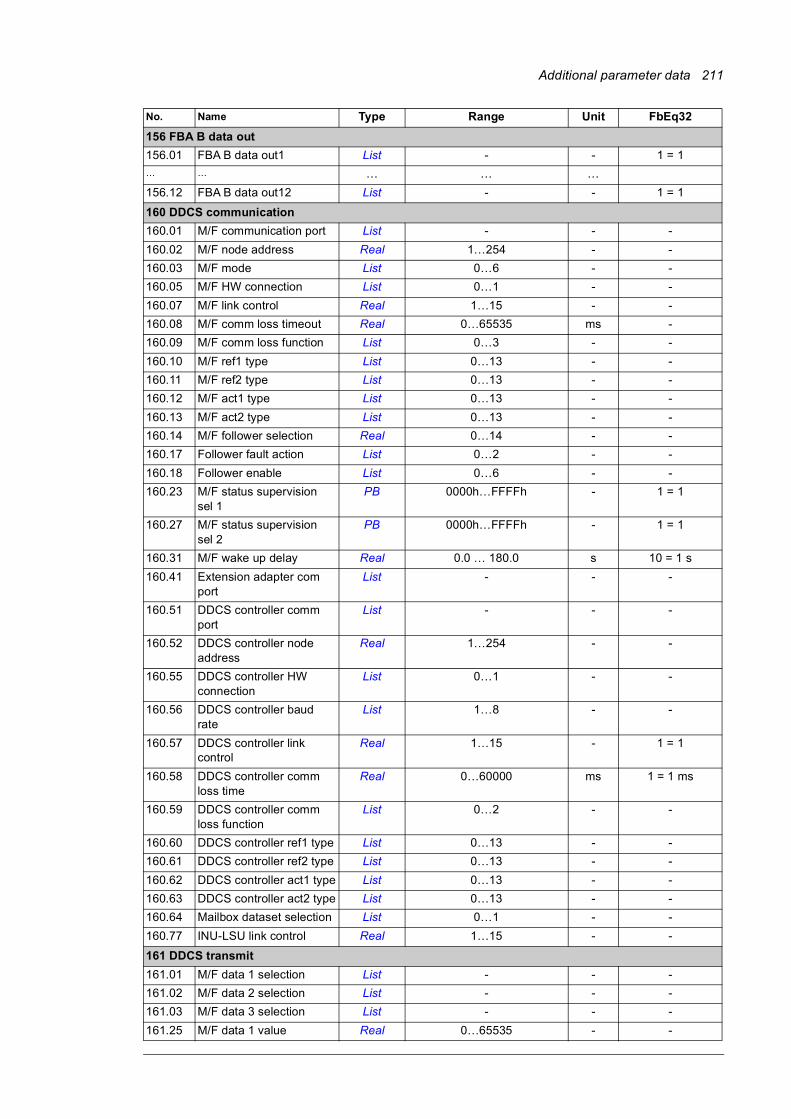
Additional parameter data 211
156 FBA B data out
156.01 FBA B data out1 List - - 1 = 1
… … … … …
156.12 FBA B data out12 List - - 1 = 1
160 DDCS communication
160.01 M/F communication port List - - -
160.02 M/F node address Real 1…254 - -
160.03 M/F mode List 0…6 - -
160.05 M/F HW connection List 0…1 - -
160.07 M/F link control Real 1…15 - -
160.08 M/F comm loss timeout Real 0…65535 ms -
160.09 M/F comm loss function List 0…3 - -
160.10 M/F ref1 type List 0…13 - -
160.11 M/F ref2 type List 0…13 - -
160.12 M/F act1 type List 0…13 - -
160.13 M/F act2 type List 0…13 - -
160.14 M/F follower selection Real 0…14 - -
160.17 Follower fault action List 0…2 - -
160.18 Follower enable List 0…6 - -
160.23 M/F status supervision sel 1
PB 0000h…FFFFh - 1 = 1
160.27 M/F status supervision sel 2
PB 0000h…FFFFh - 1 = 1
160.31 M/F wake up delay Real 0.0 … 180.0 s 10 = 1 s
160.41 Extension adapter com port
List - - -
160.51 DDCS controller comm port
List - - -
160.52 DDCS controller node address
Real 1…254 - -
160.55 DDCS controller HW connection
List 0…1 - -
160.56 DDCS controller baud rate
List 1…8 - -
160.57 DDCS controller link control
Real 1…15 - 1 = 1
160.58 DDCS controller comm loss time
Real 0…60000 ms 1 = 1 ms
160.59 DDCS controller comm loss function
List 0…2 - -
160.60 DDCS controller ref1 type List 0…13 - -
160.61 DDCS controller ref2 type List 0…13 - -
160.62 DDCS controller act1 type List 0…13 - -
160.63 DDCS controller act2 type List 0…13 - -
160.64 Mailbox dataset selection List 0…1 - -
160.77 INU-LSU link control Real 1…15 - -
161 DDCS transmit
161.01 M/F data 1 selection List - - -
161.02 M/F data 2 selection List - - -
161.03 M/F data 3 selection List - - -
161.25 M/F data 1 value Real 0…65535 - -
No. Name Type Range Unit FbEq32

212 Additional parameter data
161.26 M/F data 2 value Real 0…65535 - -
161.27 M/F data 3 value Real 0…65535 - -
161.51 Data set 11 data 1 selection
List 0…24 - -
161.52 Data set 11 data 2 selection
List 0…24 - -
161.53 Data set 11 data 3 selection
List 0…24 - -
161.54 Data set 13 data 1 selection
List 0…24 - -
161.55 Data set 13 data 2 selection
List 0…24 - -
161.56 Data set 13 data 3 selection
List 0…24 - -
161.57 Data set 15 data 1 selection
List 0…24 - -
161.58 Data set 15 data 2 selection
List 0…24 - -
161.59 Data set 15 data 3 selection
List 0…24 - -
161.60 Data set 17 data 1 selection
List 0…24 - -
161.61 Data set 17 data 2 selection
List 0…24 - -
161.62 Data set 17 data 3 selection
List 0…24 - -
161.63 Data set 19 data 1 selection
List 0…24 - -
161.64 Data set 19 data 2 selection
List 0…24 - -
161.65 Data set 19 data 3 selection
List 0…24 - -
161.66 Data set 21 data 1 selection
List 0…24 - -
161.67 Data set 21 data 2 selection
List 0…24 - -
161.68 Data set 21 data 3 selection
List 0…24 - -
161.69 Data set 23 data 1 selection
List 0…24 - -
161.70 Data set 23 data 2 selection
List 0…24 - -
161.71 Data set 23 data 3 selection
List 0…24 - -
161.72 Data set 25 data 1 selection
List 0…24 - -
161.73 Data set 25 data 2 selection
List 0…24 - -
161.74 Data set 25 data 3 selection
List 0…24 - -
161.101 Data set 11 data 1 value Real 0…65535 - 1 = 1
161.102 Data set 11 data 2 value Real 0…65535 - 1 = 1
161.103 Data set 11 data 3 value Real 0…65535 - 1 = 1
161.104 Data set 13 data 1 value Real 0…65535 - 1 = 1
No. Name Type Range Unit FbEq32

Additional parameter data 213
161.105 Data set 13 data 2 value Real 0…65535 - 1 = 1
161.106 Data set 13 data 3 value Real 0…65535 - 1 = 1
161.107 Data set 15 data 1 value Real 0…65535 - 1 = 1
161.108 Data set 15 data 2 value Real 0…65535 - 1 = 1
161.109 Data set 15 data 3 value Real 0…65535 - 1 = 1
161.110 Data set 17 data 1 value Real 0…65535 - 1 = 1
161.111 Data set 17 data 2 value Real 0…65535 - 1 = 1
161.112 Data set 17 data 3 value Real 0…65535 - 1 = 1
161.113 Data set 19 data 1 value Real 0…65535 - 1 = 1
161.114 Data set 19 data 2 value Real 0…65535 - 1 = 1
161.115 Data set 19 data 3 value Real 0…65535 - 1 = 1
161.116 Data set 21 data 1 value Real 0…65535 - 1 = 1
161.117 Data set 21 data 2 value Real 0…65535 - 1 = 1
161.118 Data set 21 data 3 value Real 0…65535 - 1 = 1
161.119 Data set 23 data 1 value Real 0…65535 - 1 = 1
161.120 Data set 23 data 2 value Real 0…65535 - 1 = 1
161.121 Data set 23 data 3 value Real 0…65535 - 1 = 1
161.122 Data set 25 data 1 value Real 0…65535 - 1 = 1
161.123 Data set 25 data 2 value Real 0…65535 - 1 = 1
161.124 Data set 25 data 3 value Real 0…65535 - 1 = 1
162 DDCS receive
162.01 M/F data 1 selection List - - -
162.02 M/F data 2 selection List - - -
162.03 M/F data 3 selection List - - -
162.04 Follower node 2 data 1 sel List - - -
162.05 Follower node 2 data 2 sel List - - -
162.06 Follower node 2 data 3 sel List - - -
162.07 Follower node 3 data 1 sel List - - -
162.08 Follower node 3 data 2 sel List - - -
162.09 Follower node 3 data 3 sel List - - -
162.10 Follower node 4 data 1 sel List - - -
162.11 Follower node 4 data 2 sel List - - -
162.12 Follower node 4 data 3 sel List - - -
162.25 MF data 1 value Real 0…65535 - -
162.26 MF data 2 value Real 0…65535 - -
162.27 MF data 3 value Real 0…65535 - -
162.28 Follower node 2 data 1 value
Real 0…65535 - -
162.29 Follower node 2 data 2 value
Real 0…65535 - -
162.30 Follower node 2 data 3 value
Real 0…65535 - -
162.31 Follower node 3 data 1 value
Real 0…65535 - -
162.32 Follower node 3 data 2 value
Real 0…65535 - -
162.33 Follower node 3 data 3 value
Real 0…65535 - -
162.34 Follower node 4 data 1 value
Real 0…65535 - -
No. Name Type Range Unit FbEq32

214 Additional parameter data
162.35 Follower node 4 data 2 value
Real 0…65535 - -
162.36 Follower node 4 data 3 value
Real 0…65535 - -
162.37 M/F communication status 1
PB 0000h…FFFFh - 1 = 1
162.38 M/F communication status 2
PB 0000h…FFFFh - 1 = 1
162.41 M/F follower ready status 1
PB 0000h…FFFFh - 1 = 1
162.42 M/F follower ready status 2
PB 0000h…FFFFh - 1 = 1
162.51 Data set 10 data 1 selection
List 0…21 - -
162.52 Data set 10 data 2 selection
List 0…21 - -
162.53 Data set 10 data 3 selection
List 0…21 - -
162.54 Data set 12 data 1 selection
List 0…21 - -
162.55 Data set 12 data 2 selection
List 0…21 - -
162.56 Data set 12 data 3 selection
List 0…21 - -
162.57 Data set 14 data 1 selection
List 0…21 - -
162.58 Data set 14 data 2 selection
List 0…21 - -
162.59 Data set 14 data 3 selection
List 0…21 - -
162.60 Data set 16 data 1 selection
List 0…21 - -
162.61 Data set 16 data 2 selection
List 0…21 - -
162.62 Data set 16 data 3 selection
List 0…21 - -
162.63 Data set 18 data 1 selection
List 0…21 - -
162.64 Data set 18 data 2 selection
List 0…21 - -
162.65 Data set 18 data 3 selection
List 0…21 - -
162.66 Data set 20 data 1 selection
List 0…21 - -
162.67 Data set 20 data 2 selection
List 0…21 - -
162.68 Data set 20 data 3 selection
List 0…21 - -
162.69 Data set 22 data 1 selection
List 0…21 - -
162.70 Data set 22 data 2 selection
List 0…21 - -
162.71 Data set 22 data 3 selection
List 0…21 - -
No. Name Type Range Unit FbEq32

Additional parameter data 215
162.72 Data set 24 data 1 selection
List 0…21 - -
162.73 Data set 24 data 2 selection
List 0…21 - -
162.74 Data set 24 data 3 selection
List 0…21 - -
162.101 Data set 10 data 1 value Real 0…65535 - 1 = 1
162.102 Data set 10 data 2 value Real 0…65535 - 1 = 1
162.103 Data set 10 data 3 value Real 0…65535 - 1 = 1
162.104 Data set 12 data 1 value Real 0…65535 - 1 = 1
162.105 Data set 12 data 2 value Real 0…65535 - 1 = 1
162.106 Data set 12 data 3 value Real 0…65535 - 1 = 1
162.107 Data set 14 data 1 value Real 0…65535 - 1 = 1
162.108 Data set 14 data 2 value Real 0…65535 - 1 = 1
162.109 Data set 14 data 3 value Real 0…65535 - 1 = 1
162.110 Data set 16 data 1 value Real 0…65535 - 1 = 1
162.111 Data set 16 data 2 value Real 0…65535 - 1 = 1
162.112 Data set 16 data 3 value Real 0…65535 - 1 = 1
162.113 Data set 18 data 1 value Real 0…65535 - 1 = 1
162.114 Data set 18 data 2 value Real 0…65535 - 1 = 1
162.115 Data set 18 data 3 value Real 0…65535 - 1 = 1
162.116 Data set 20 data 1 value Real 0…65535 - 1 = 1
162.117 Data set 20 data 2 value Real 0…65535 - 1 = 1
162.118 Data set 20 data 3 value Real 0…65535 - 1 = 1
162.119 Data set 22 data 1 value Real 0…65535 - 1 = 1
162.120 Data set 22 data 2 value Real 0…65535 - 1 = 1
162.121 Data set 22 data 3 value Real 0…65535 - 1 = 1
162.122 Data set 24 data 1 value Real 0…65535 - 1 = 1
162.123 Data set 24 data 2 value Real 0…65535 - 1 = 1
162.124 Data set 24 data 3 value Real 0…65535 - 1 = 1
190 BAMU measurements
190.01 Phase voltage U1 Real 0.00…2000.00 V 100 = 1 V
190.02 Phase voltage V1 Real 0.00…2000.00 V 100 = 1 V
190.03 Phase voltage W1 Real 0.00…2000.00 V 100 = 1 V
190.06 Mains voltage U1-V1 Real 0.00…2000.00 V 100 = 1 V
190.07 Mains voltage V1-W1 Real 0.00…2000.00 V 100 = 1 V
190.08 Mains voltage W1-U1 Real 0.00…2000.00 V 100 = 1 V
190.15 Frequency 1 Real 0.00…100.00 Hz 100 = 1 Hz
190.20 Phase voltage U2 Real 0.00…2000.00 V 100 = 1 V
190.21 Phase voltage V2 Real 0.00…2000.00 V 100 = 1 V
190.22 Phase voltage W2 Real 0.00…2000.00 V 100 = 1 V
190.25 Mains voltage U2-V2 Real 0.00…2000.00 V 100 = 1 V
190.26 Mains voltage V2-W2 Real 0.00…2000.00 V 100 = 1 V
190.27 Mains voltage W2-U2 Real 0.00…2000.00 V 100 = 1 V
190.34 Frequency 2 Real 0.00…100.00 Hz 100 = 1 Hz
190.40 Phase current U1 Real - A 100 = 1 A
190.41 Phase current V1 Real - A 100 = 1 A
190.42 Phase current W1 Real - A 100 = 1 A
No. Name Type Range Unit FbEq32

216 Additional parameter data
191 BAMU configuration
191.01 U1 measurement List 0…1 - 1 = 1
191.02 U1 meas type List 1…3 - 1 = 1
191.05 U1 measurement location List 0…1 - 1 = 1
191.10 U2 measurement List 0…1 - 1 = 1
191.11 U2 meas type List 1…3 - 1 = 1
191.20 I measurement List 0…1 - 1 = 1
191.22 Current transf. ratio Real - - 1 = 1
191.29 Board type List 0…65535 - 1 = 1
191.30 BAMU 1 channel Real 0…12 - 1 = 1
195 HW configuration
195.01 Supply voltage List 0…6 - 1 = 1
195.04 Control board supply List 0…2 - 1 = 1
195.09 Switch fuse controller List 0…2 - 1 = 1
195.13 Reduced run mode List 0…65535 - 1 = 1
195.14 Connected modules PB 0000h…FFFFh - 1 = 1
195.16 Router mode List - - 1 = 1
195.17 Router channel config PB 0000h…FFFFh - 1 = 1
195.20 HW options word 1 PB 0000h…FFFFh - 1 = 1
195.30 Parallel type list filter List 1…4 - 1 = 1
195.31 Parallel connection rating id
List - - 1 = 1
195.51 Current offset calibration List 0…1 - 1 = 1
196 System
196.01 Language List - - 1 = 1
196.02 Pass code Data 0 - 1 = 1
196.03 Access levels active PB 0000h…FFFFh - 1 = 1
196.06 Parameter restore List - - 1 = 1
196.07 Parameter save manually List 0…1 - 1 = 1
196.08 Control board boot Real 0…1 - 1 = 1
196.10 User set status List - - 1 = 1
196.11 User set save/load List - - 1 = 1
196.12 User set I/O mode in1 Binary src - - 1 = 1
196.13 User set I/O mode in2 Binary src - - 1 = 1
196.20 Time sync primary source List 0…10 - 1 = 1
196.24 Full days since 1st Jan 1980
Real 1…59999 - 1 = 1
196.25 Time in minutes within 24 h
Real 0…1439 - 1 = 1
196.26 Time in ms within one minute
Real 0…59999 - 1 = 1
196.29 Time sync source status PB 0000h…FFFFh - 1 = 1
196.39 Power up event logging List 0…1 - 1 = 1
196.61 User data logger status word
PB 0000h…FFFFh - 1 = 1
196.63 User data logger trigger Binary src - - -
196.64 User data logger start Binary src - - -
196.65 Factory data logger time level
List - - 1 = 1
196.70 Disable adaptive program Data 0…1 - 1 = 1
No. Name Type Range Unit FbEq32
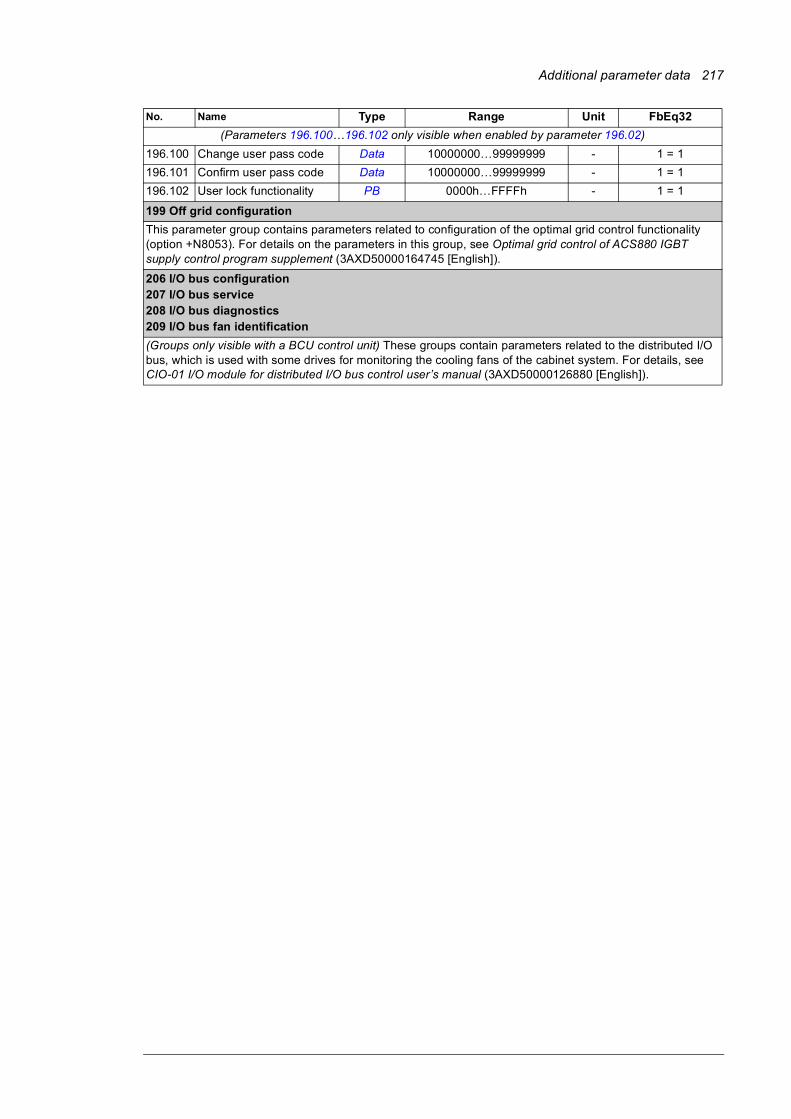
Additional parameter data 217
(Parameters 196.100…196.102 only visible when enabled by parameter 196.02)
196.100 Change user pass code Data 10000000…99999999 - 1 = 1
196.101 Confirm user pass code Data 10000000…99999999 - 1 = 1
196.102 User lock functionality PB 0000h…FFFFh - 1 = 1
199 Off grid configuration
This parameter group contains parameters related to configuration of the optimal grid control functionality (option +N8053). For details on the parameters in this group, see Optimal grid control of ACS880 IGBT supply control program supplement (3AXD50000164745 [English]).
206 I/O bus configuration207 I/O bus service208 I/O bus diagnostics209 I/O bus fan identification
(Groups only visible with a BCU control unit) These groups contain parameters related to the distributed I/O bus, which is used with some drives for monitoring the cooling fans of the cabinet system. For details, see CIO-01 I/O module for distributed I/O bus control user’s manual (3AXD50000126880 [English]).
No. Name Type Range Unit FbEq32

218 Additional parameter data
Fault tracing 219
8
Fault tracing
What this chapter containsThe chapter lists the warning and fault messages including possible causes and corrective actions. The causes of most warnings and faults can be identified and corrected using the information in this chapter. If not, an ABB service representative should be contacted.
Warnings and faults are listed below in separate tables. Each table is sorted by warning/fault code.
Safety
WARNING! Only qualified electricians are allowed to service the IGBT supply unit. See ACS880 multidrive cabinets and modules safety instructions (3AUA0000102301 [English]).

220 Fault tracing
Indications
Warnings and faults
Warnings and faults indicate an abnormal status. The codes and names of active warnings/faults are displayed on the control panel as well as the Drive composer PC tool. Only the codes of warnings/faults are available over fieldbus.
Warnings do not need to be reset; they stop showing when the cause of the warning ceases. After the cause of the fault has been corrected, the active fault can be reset from the control panel or Drive composer PC tool. The control panel can be in local or remote (external) control mode. When the fault has been removed, the supply unit can be restarted. Faults can also be reset from an external source selected by parameter 131.11 Fault reset selection.
Warning and fault indications can be directed to a relay output or a digital input/output by selecting Warning, Fault or Fault (-1) in the source selection parameter. See sections• Programmable digital inputs and outputs (page 25)
• Programmable relay outputs (page 25), and
• Programmable I/O extensions (page 26).
Pure events
In addition to warnings and faults, there are pure events that are only recorded in the event logs. The codes of these events are included in the Warning messages table.
Editable messages
For some warnings and faults, the message text can be edited and instructions and contact information added. To edit these messages, choose Menu - Settings - Edit texts on the control panel or Drive composer pro PC tool.
Warning/fault history and analysis
Event logs
The IGBT supply unit has two event logs that can be accessed from the main Menu on the control panel. The logs can also be accessed (and reset) using the Drive composer PC tool.
One of the logs contains faults and fault resets. The other log lists warnings and pure events, as well as clearing entries. Both logs contain the 64 most recent events. All indications are stored in the event logs with a time stamp and other information.
Auxiliary codes
Some events generate an auxiliary code that often helps in pinpointing the problem. The auxiliary code is displayed on the control panel together with the message. It is also stored in the event log details. In the Drive composer PC tool, the auxiliary code (if any) is shown in the event listing.

Fault tracing 221
Factory data logger
The supply unit has a data logger that samples preselected values at 500-microsecond (default; see parameter 196.65 Factory data logger time level) intervals. By default, approximately 700 samples recorded immediately before and after a fault are saved to the memory unit of the supply unit. The fault data of the last five faults is accessible in the event log when viewed in the Drive composer pro PC tool. (The fault data is not accessible through the control panel.)
The values that are recorded in the factory data log are 101.01 DC voltage, 101.09 Grid voltage, 101.21 Converter current %, 101.12 Power, 101.15 Reactive power %, 106.01 Main control word, 130.01 Limit word 1, 130.03 Limit word 3 and 106.11 Main status word. The selection of parameters cannot be changed by the user.
Other data loggers
User data logger
A custom data logger can be configured using the Drive composer pro PC tool. This functionality enables the free selection of up to eight parameters to be sampled at selectable intervals. The triggering conditions and the length of the monitoring period can also be defined by the user within the limit of approximately 8000 samples. In addition to the PC tool, the status of the logger is shown by parameter 196.61 User data logger status word. The triggering sources can be selected by parameters 196.63 User data logger trigger and 196.64 User data logger start). The configuration, status and collected data is saved to the memory unit for later analysis.
PSL2 data logger
The BCU control unit used with certain supply unit types (especially those with parallel-connected supply modules) contains a data logger that collects data from the supply modules to help fault tracing and analysis. The data is saved onto the SD memory card attached to the BCU, and can be analyzed by ABB service personnel.
Parameters that contain warning/fault information
The codes of active warnings and faults (maximum five each), and five previously occurred warnings and faults are stored in the parameters 104.01…104.20.

222 Fault tracing
Fault and warning wordsWith fault and warning words, it is possible to read status of multiple events simultaneously. 16-bit fault word 104.21 Fault word 1 shows activity of some predefined faults. 16-bit warning word 104.31 Warning word 1 shows activity of some predefined warnings. 16-bit event word 104.40 Event word 1 shows activity of user-configurable events. Each bit of 104.40 Event word 1 is configurable by event (basic) code, and optionally auxiliary code. If auxiliary code is set to zero, all auxiliary codes are accepted. Configuration of 104.40 Event word 1 is done by parameters 104.41…104.72.
Bits 3, 8 and 10 of 104.21 Fault word 1 can indicate several events as listed below. Also, bits 0 and 3 of 104.31 Warning word 1 can indicate several events as listed below. To use these bits, the user selects one of the codes listed below in that bit.
104.21 Fault word 1, bit 3
Code and nameCFE0 Power unit temperature
• 2E04 IGBT overload
• 4E02 IGBT temperature
• 4E01 Cooling
• 4E03 Excess temperature
• 4E04 Excess temperature difference
104.21 Fault word 1, bit 8
Code and nameCFE1 Internal system fault
• 6E03 Task overload
• 6E04 Stack overflow
• 6E05 Internal file load
• 6E06 Internal record load
• 6E07 Application loading
• 6E09 Internal SSW fault
• 6E0B Kernel overload
• 6E15 Text data overflow
• 6E16 Text 32-bit table overflow
• 6E17 Text 64-bit table overflow
• 6E18 Text file overflow
• 6E1D Internal error
104.21 Fault word 1, bit 10
Code and nameCFE3 Field bus comm
• 7E0B FBA A communication
• 7E0C FBA B communication
• 7E11 DDCS controller comm loss

Fault tracing 223
104.31 Warning word 1, bit 0
Code and nameCFE4 Field bus comm
• AE30 FBA A communication
• AE31 FBA B communication
• AE6D DDCS controller comm loss
104.31 Warning word 1, bit 3
Code and nameCFE2 Power unit temperature
• AE12 IGBT overtemperature
• AE13 Cooling
• AE14 Excess temperature
• AE15 Excess temperature difference
• AE16 IGBT temperature
• AE04 IGBT overload

224 Fault tracing
Warning messagesCode (hex)
Warning Cause What to do
AE00 Current calibration Current offset and gain measurement calibration will occur at next start.
Informative warning.
AE01 Overcurrent Output current has exceeded internal fault limit.
Check supply voltage.
Check that there are no power factor correction capacitors or surge absorbers in supply cable.
Check motor load and acceleration times.
Check power semiconductors (IGBTs) and current transducers.
Check the auxiliary code (format XXXY YYZZ). With parallel-connected supply modules, “Y YY” specifies through which BCU control unit channel the fault was received. “ZZ” indicates the phase that triggered the fault (0: No detailed information available, 1: U-phase, 2: V-phase, 4: W-phase, 3/5/6/7: multiple phases).
AE02 Earth leakageProgrammable warning: 131.20 Earth fault
IGBT supply has detected load unbalance.
Check AC fuses.
Check for earth leakages.
Check supply cabling.
Check power modules.
Check there are no power factor correction capacitors or surge absorbers in supply cable.
AE03 Short circuit IGBT supply has detected short circuit.
Check supply cable.
Check there are no power factor correction capacitors or surge absorbers in supply cable.
AE04 IGBT overload Excessive IGBT junction to case temperature.
Check supply cable.
AE05 BU current difference Current difference detected by the branching unit (BU).
Check converter fuses.
Check converter(s).
Check inverter(s).
Check LCL filter.
AE06 BU earth leakage Earth leakage detected by the branching unit: sum of all currents exceeds the level.
Check AC fuses.
Check for earth leakages.
Check supply cabling.
Check power modules.
Check there are no power factor correction capacitors or surge absorbers in supply cable.
AE09 DC link overvoltage Excessive intermediate circuit DC voltage.
Note: This warning can be shown only when the IGBT supply unit is not modulating.
Check that parameter 195.01 Supply voltage is set according to the supply voltage in use.
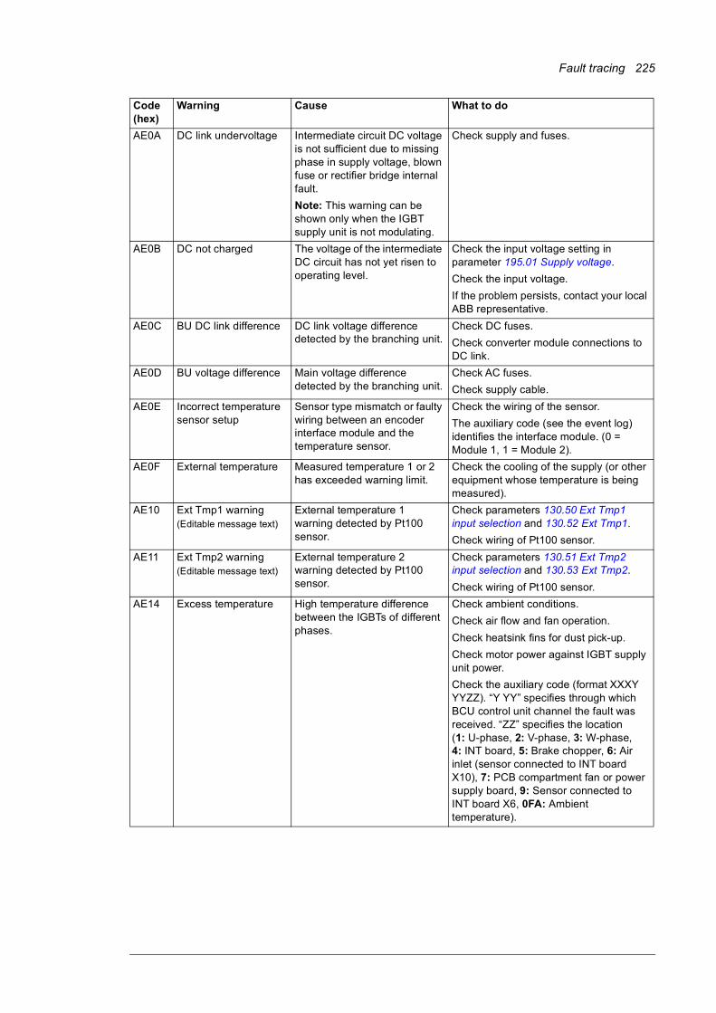
Fault tracing 225
AE0A DC link undervoltage Intermediate circuit DC voltage is not sufficient due to missing phase in supply voltage, blown fuse or rectifier bridge internal fault.
Note: This warning can be shown only when the IGBT supply unit is not modulating.
Check supply and fuses.
AE0B DC not charged The voltage of the intermediate DC circuit has not yet risen to operating level.
Check the input voltage setting in parameter 195.01 Supply voltage.
Check the input voltage.
If the problem persists, contact your local ABB representative.
AE0C BU DC link difference DC link voltage difference detected by the branching unit.
Check DC fuses.
Check converter module connections to DC link.
AE0D BU voltage difference Main voltage difference detected by the branching unit.
Check AC fuses.
Check supply cable.
AE0E Incorrect temperature sensor setup
Sensor type mismatch or faulty wiring between an encoder interface module and the temperature sensor.
Check the wiring of the sensor.
The auxiliary code (see the event log) identifies the interface module. (0 = Module 1, 1 = Module 2).
AE0F External temperature Measured temperature 1 or 2 has exceeded warning limit.
Check the cooling of the supply (or other equipment whose temperature is being measured).
AE10 Ext Tmp1 warning(Editable message text)
External temperature 1 warning detected by Pt100 sensor.
Check parameters 130.50 Ext Tmp1 input selection and 130.52 Ext Tmp1.
Check wiring of Pt100 sensor.
AE11 Ext Tmp2 warning(Editable message text)
External temperature 2 warning detected by Pt100 sensor.
Check parameters 130.51 Ext Tmp2 input selection and 130.53 Ext Tmp2.
Check wiring of Pt100 sensor.
AE14 Excess temperature High temperature difference between the IGBTs of different phases.
Check ambient conditions.
Check air flow and fan operation.
Check heatsink fins for dust pick-up.
Check motor power against IGBT supply unit power.
Check the auxiliary code (format XXXY YYZZ). “Y YY” specifies through which BCU control unit channel the fault was received. “ZZ” specifies the location (1: U-phase, 2: V-phase, 3: W-phase, 4: INT board, 5: Brake chopper, 6: Air inlet (sensor connected to INT board X10), 7: PCB compartment fan or power supply board, 9: Sensor connected to INT board X6, 0FA: Ambient temperature).
Code (hex)
Warning Cause What to do
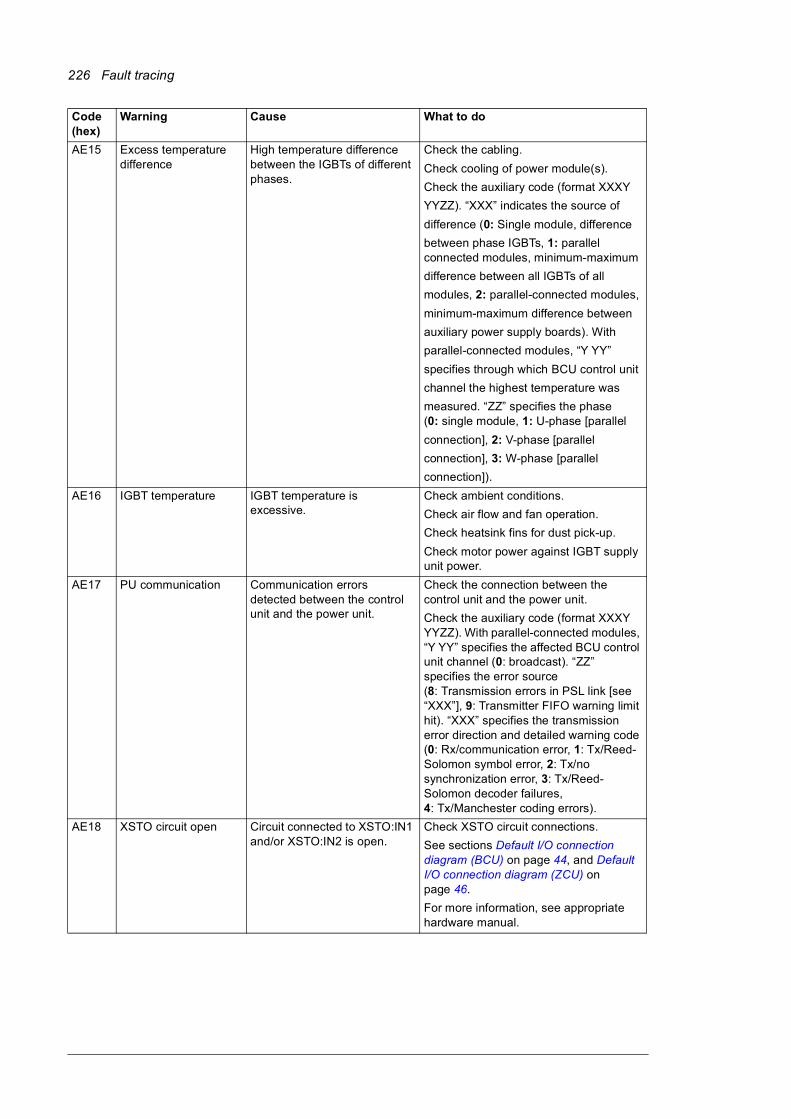
226 Fault tracing
AE15 Excess temperature difference
High temperature difference between the IGBTs of different phases.
Check the cabling.
Check cooling of power module(s).
Check the auxiliary code (format XXXY
YYZZ). “XXX” indicates the source of
difference (0: Single module, difference
between phase IGBTs, 1: parallel connected modules, minimum-maximum
difference between all IGBTs of all
modules, 2: parallel-connected modules,
minimum-maximum difference between
auxiliary power supply boards). With
parallel-connected modules, “Y YY”
specifies through which BCU control unit
channel the highest temperature was
measured. “ZZ” specifies the phase (0: single module, 1: U-phase [parallel
connection], 2: V-phase [parallel
connection], 3: W-phase [parallel
connection]).
AE16 IGBT temperature IGBT temperature is excessive.
Check ambient conditions.
Check air flow and fan operation.
Check heatsink fins for dust pick-up.
Check motor power against IGBT supply unit power.
AE17 PU communication Communication errors detected between the control unit and the power unit.
Check the connection between the control unit and the power unit.
Check the auxiliary code (format XXXY YYZZ). With parallel-connected modules, “Y YY” specifies the affected BCU control unit channel (0: broadcast). “ZZ” specifies the error source (8: Transmission errors in PSL link [see “XXX”], 9: Transmitter FIFO warning limit hit). “XXX” specifies the transmission error direction and detailed warning code (0: Rx/communication error, 1: Tx/Reed- Solomon symbol error, 2: Tx/no synchronization error, 3: Tx/Reed- Solomon decoder failures, 4: Tx/Manchester coding errors).
AE18 XSTO circuit open Circuit connected to XSTO:IN1 and/or XSTO:IN2 is open.
Check XSTO circuit connections.
See sections Default I/O connection diagram (BCU) on page 44, and Default I/O connection diagram (ZCU) on page 46.
For more information, see appropriate hardware manual.
Code (hex)
Warning Cause What to do
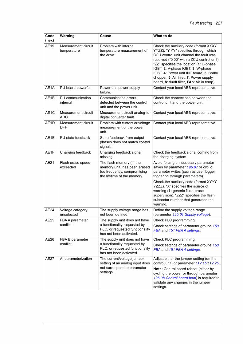
Fault tracing 227
AE19 Measurement circuit temperature
Problem with internal temperature measurement of the drive.
Check the auxiliary code (format XXXY YYZZ). “Y YY” specifies through which BCU control unit channel the fault was received (“0 00” with a ZCU control unit). “ZZ” specifies the location (1: U-phase IGBT, 2: V-phase IGBT, 3: W-phase IGBT, 4: Power unit INT board, 5: Brake chopper, 6: Air inlet, 7: Power supply board, 8: du/dt filter, FAh: Air in temp).
AE1A PU board powerfail Power unit power supply failure.
Contact your local ABB representative.
AE1B PU communication internal
Communication errors detected between the control unit and the power unit.
Check the connections between the control unit and the power unit.
AE1C Measurement circuit ADC
Measurement circuit analog-to-digital converter fault.
Contact your local ABB representative.
AE1D Measurement circuit DFF
Problem with current or voltage measurement of the power unit.
Contact your local ABB representative.
AE1E PU state feedback State feedback from output phases does not match control signals.
Contact your local ABB representative.
AE1F Charging feedback Charging feedback signal missing.
Check the feedback signal coming from the charging system.
AE21 Flash erase speed exceeded
The flash memory (in the memory unit) has been erased too frequently, compromising the lifetime of the memory.
Avoid forcing unnecessary parameter saves by parameter 196.07 or cyclic parameter writes (such as user logger triggering through parameters).
Check the auxiliary code (format XYYY YZZZ). “X” specifies the source of warning (1: generic flash erase supervision). “ZZZ” specifies the flash subsector number that generated the warning.
AE24 Voltage category unselected
The supply voltage range has not been defined.
Define the supply voltage range (parameter 195.01 Supply voltage).
AE25 FBA A parameter conflict
The supply unit does not have a functionality requested by PLC, or requested functionality has not been activated.
Check PLC programming.
Check settings of parameter groups 150 FBA and 151 FBA A settings.
AE26 FBA B parameter conflict
The supply unit does not have a functionality requested by PLC, or requested functionality has not been activated.
Check PLC programming.
Check settings of parameter groups 150 FBA and 151 FBA A settings.
AE27 AI parameterization The current/voltage jumper setting of an analog input does not correspond to parameter settings.
Adjust either the jumper setting (on the control unit) or parameter 112.15/112.25.
Note: Control board reboot (either by cycling the power or through parameter 196.08 Control board boot) is required to validate any changes in the jumper settings.
Code (hex)
Warning Cause What to do
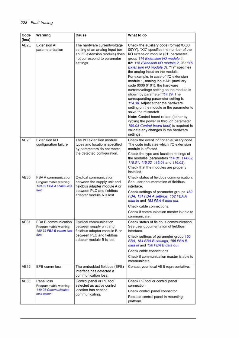
228 Fault tracing
AE2E Extension AI parameterization
The hardware current/voltage setting of an analog input (on an I/O extension module) does not correspond to parameter settings.
Check the auxiliary code (format XX00 00YY). “XX” specifies the number of the I/O extension module (01: parameter group 114 Extension I/O module 1, 02: 115 Extension I/O module 2, 03: 116 Extension I/O module 3). “YY” specifies the analog input on the module.For example, in case of I/O extension module 1, analog input AI1 (auxiliary code 0000 0101), the hardware current/voltage setting on the module is shown by parameter 114.29. The corresponding parameter setting is 114.30. Adjust either the hardware setting on the module or the parameter to solve the mismatch.Note: Control board reboot (either by cycling the power or through parameter 196.08 Control board boot) is required to validate any changes in the hardware settings.
AE2F Extension I/O configuration failure
The I/O extension module types and locations specified by parameters do not match the detected configuration.
Check the event log for an auxiliary code. The code indicates which I/O extension module is affected.Check the type and location settings of the modules (parameters 114.01, 114.02, 115.01, 115.02, 116.01 and 116.02).Check that the modules are properly installed.
AE30 FBA A communicationProgrammable warning:150.02 FBA A comm loss func
Cyclical communication between the supply unit and fieldbus adapter module A or between PLC and fieldbus adapter module A is lost.
Check status of fieldbus communication. See user documentation of fieldbus interface.
Check settings of parameter groups 150 FBA, 151 FBA A settings, 152 FBA A data in and 153 FBA A data out.
Check cable connections.
Check if communication master is able to communicate.
AE31 FBA B communicationProgrammable warning:150.32 FBA B comm loss func
Cyclical communication between supply unit and fieldbus adapter module B or between PLC and fieldbus adapter module B is lost.
Check status of fieldbus communication. See user documentation of fieldbus interface.
Check settings of parameter group 150 FBA, 154 FBA B settings, 155 FBA B data in and 156 FBA B data out.
Check cable connections.
Check if communication master is able to communicate.
AE32 EFB comm loss The embedded fieldbus (EFB) interface has detected a communication loss.
Contact your local ABB representative.
AE3E Panel lossProgrammable warning:149.05 Communication loss action
Control panel or PC tool selected as active control location has ceased communicating.
Check PC tool or control panel connection.
Check control panel connector.
Replace control panel in mounting platform.
Code (hex)
Warning Cause What to do

Fault tracing 229
AE40 Output relay warning Warning generated by an edge counter.Programmable warnings:133.35 Edge counter 1 warning selection133.45 Edge counter 2 warning selection
Check the event log for an auxiliary code. Check the source of the warning corresponding to the code:2: 133.33 Edge counter 1 source3: 133.43 Edge counter 2 source.
AE41 Supply unit starts warning
AE42 Power ups warning
AE43 Main contactor warning
AE44 DC charge warning
AE45 On-Time 1 warning(Editable message text)Programmable warning:133.14 On-time 1 warning select
Warning generated by on-time timer 1.
Check the source of the warning (parameter 133.13 On-time 1 source).
AE46 On-Time 2 warning(Editable message text)Programmable warning:133.24 On-time 2 warning select
Warning generated by on-time timer 2.
Check the source of the warning (parameter 133.23 On-time 2 source).
AE47 Edge counter 1 warning(Editable message text)Programmable warning:133.35 Edge counter 1 warning selection
Warning generated by edge counter 1.
Check the source of the warning (parameter 133.33 Edge counter 1 source).
AE48 Edge counter 2 warning(Editable message text)Programmable warning:133.45 Edge counter 2 warning selection
Warning generated by edge counter 2.
Check the source of the warning (parameter 133.43 Edge counter 2 source).
AE49 Value counter 1 warning(Editable message text)Programmable warning:133.55 Value counter 1 warning select
Warning generated by value counter 1.
Check the source of the warning (parameter 133.53 Value counter 1 source).
AE4A Value counter 2 warning(Editable message text)Programmable warning:133.65 Value counter 2 warning selection
Warning generated by value counter 2.
Check the source of the warning (parameter 133.63 Value counter 2 source).
AE4B Device clean warning Warning generated by an on-time timer.Programmable warnings:133.14 On-time 1 warning select133.24 On-time 2 warning select
Check the event log for an auxiliary code. Check the source of the warning corresponding to the code:0: 133.13 On-time 1 source1: 133.23 On-time 2 source10: 105.04 Fan on-time counter.
AE4C DC capacitor warning
AE4D Cabinet fan warning
AE4E Cooling fan warning
AE4F Additional cooling fan warning
AE51 External warning 1Programmable warning:131.01 External event 1 source131.02 External event 1 type
Warning generated by external device 1. (This information is configured through one of programmable digital inputs.)
Check external devices.
Check the setting of parameter 131.01 External event 1 source.
AE52 External warning 2Programmable fault: 131.03 External event 2 source131.04 External event 2 type
Warning generated by external device 2. (This information is configured through one of programmable digital inputs.)
Check external devices.
Check the setting of parameter 131.03 External event 2 source.
Code (hex)
Warning Cause What to do
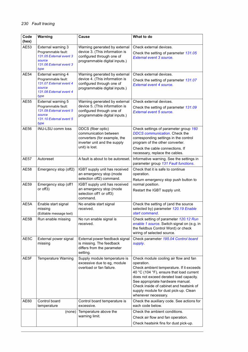
230 Fault tracing
AE53 External warning 3Programmable fault: 131.05 External event 3 source131.06 External event 3 type
Warning generated by external device 3. (This information is configured through one of programmable digital inputs.)
Check external devices.
Check the setting of parameter 131.05 External event 3 source.
AE54 External warning 4Programmable fault: 131.07 External event 4 source131.08 External event 4 type
Warning generated by external device 4. (This information is configured through one of programmable digital inputs.)
Check external devices.
Check the setting of parameter 131.07 External event 4 source.
AE55 External warning 5Programmable fault: 131.09 External event 5 source131.10 External event 5 type
Warning generated by external device 5. (This information is configured through one of programmable digital inputs.)
Check external devices.
Check the setting of parameter 131.09 External event 5 source.
AE56 INU-LSU comm loss DDCS (fiber optic) communication between converters (for example, the inverter unit and the supply unit) is lost.
Check settings of parameter group 160 DDCS communication. Check the corresponding settings in the control program of the other converter.
Check the cable connections. If necessary, replace the cables.
AE57 Autoreset A fault is about to be autoreset. Informative warning. See the settings in parameter group 131 Fault functions.
AE58 Emergency stop (off2) IGBT supply unit has received an emergency stop (mode selection off2) command.
Check that it is safe to continue operation.
Return emergency stop push button to normal position.
Restart the IGBT supply unit.
AE59 Emergency stop (off1 or off3)
IGBT supply unit has received an emergency stop (mode selection off1 or off3) command.
AE5A Enable start signal missing(Editable message text)
No enable start signal received.
Check the setting of (and the source selected by) parameter 120.19 Enable start command.
AE5B Run enable missing No run enable signal is received.
Check setting of parameter 120.12 Run enable 1 source. Switch signal on (e.g. in the fieldbus Control Word) or check wiring of selected source.
AE5C External power signal missing
External power feedback signal is missing. The feedback differs from the parameter setting.
Check parameter 195.04 Control board supply.
AE5F Temperature Warning Supply module temperature is excessive due to eg, module overload or fan failure.
Check module cooling air flow and fan operation.Check ambient temperature. If it exceeds 40 °C (104 °F), ensure that load current does not exceed derated load capacity. See appropriate hardware manual.Check inside of cabinet and heatsink of supply module for dust pick-up. Clean whenever necessary.
AE60 Control board temperature
Control board temperature is excessive.
Check the auxiliary code. See actions for each code below.
(none) Temperature above the warning limit.
Check the ambient conditions.
Check air flow and fan operation.
Check heatsink fins for dust pick-up.
Code (hex)
Warning Cause What to do

Fault tracing 231
1 Thermistor broken. Contact an ABB service representative for control unit replacement.
AE67 AI supervision An analog signal is outside the limits specified for the analog input.
Check the event log for an auxiliary code (format XYY). “X” specifies the location of the input (0: AI on control unit; 1: I/O extension module 1, etc.), “YY” specifies the input and limit (01: AI1 under minimum, 02: AI1 over maximum, 03: AI2 under minimum, 04: AI2 over maximum).Check signal level at the analog input.Check the wiring connected to the input.Check the minimum and maximum limits of the input in parameter group 112 Standard AI.
AE68 Emergency stop warning
Emergency stop warning is activated.
Check that it is safe to continue operation.
AE6D DDCS controller comm lossProgrammable warning:160.59 DDCS controller comm loss function
DDCS (fiber optic) communication between the supply unit and external controller is lost.
Check status of controller. See the user documentation of the controller.
Check settings of parameter group 160 DDCS communication.
Check cable connections. If necessary, replace cables.
AE6E Internal SW error Internal SW error Contact your local ABB representative.
Quote the auxiliary code (check the event details in the event log).
AE6F Ambient temperature Redundant measurement supervision has indicated a difference in the duplicated measurements that is outside the limits.
Contact your local ABB representative.
AE73 Fan Cooling fan is stuck or disconnected.
Check the auxiliary code to identify the fan. Code 0 denotes main fan 1. Other codes (format XYZ): “X” specifies state code (1: ID run, 2: normal). “Y” specifies the index of the converter module connected to BCU (0…n, always 0 for ZCU control units). “Z” specifies the index of the fan (1: Main fan 1, 2: Main fan 2, 3: Main fan 3, 4: Auxiliary fan 1, 5: Auxiliary fan 2, 6: Auxiliary fan 3, 7: Filter fan 1, 8: Filter fan 2, 9: Filter fan 3).
Note that modules are coded starting from 0. For example, the code 101 means that Main fan 1 of module 1 (connected to BCU channel V1T/V1R) has faulted during its ID run.
Check fan operation and connection.
Replace fan if faulty.
AE75 SD card Error related to SD card used to store data (BCU control unit only).
Check the auxiliary code. See actions for each code below.
1 No SD card Insert a compatible, writable SD card into the SD CARD slot of the BCU control unit.
2 SD card write-protected
3 SD card unreadable
Code (hex)
Warning Cause What to do
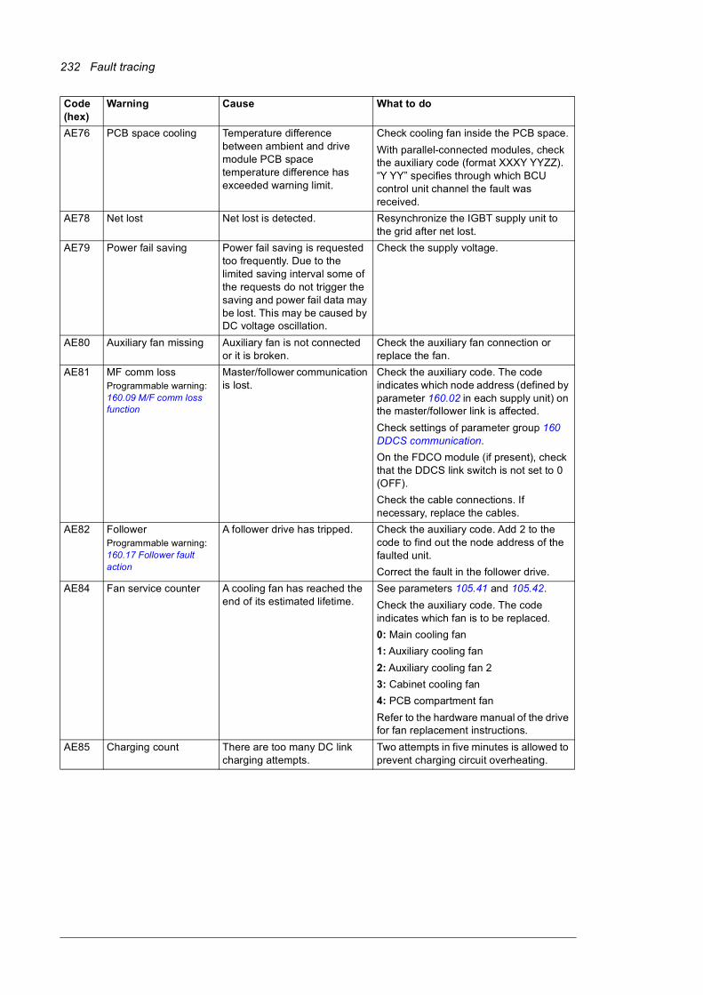
232 Fault tracing
AE76 PCB space cooling Temperature difference between ambient and drive module PCB space temperature difference has exceeded warning limit.
Check cooling fan inside the PCB space.
With parallel-connected modules, check the auxiliary code (format XXXY YYZZ). “Y YY” specifies through which BCU control unit channel the fault was received.
AE78 Net lost Net lost is detected. Resynchronize the IGBT supply unit to the grid after net lost.
AE79 Power fail saving Power fail saving is requested too frequently. Due to the limited saving interval some of the requests do not trigger the saving and power fail data may be lost. This may be caused by DC voltage oscillation.
Check the supply voltage.
AE80 Auxiliary fan missing Auxiliary fan is not connected or it is broken.
Check the auxiliary fan connection or replace the fan.
AE81 MF comm lossProgrammable warning:160.09 M/F comm loss function
Master/follower communication is lost.
Check the auxiliary code. The code indicates which node address (defined by parameter 160.02 in each supply unit) on the master/follower link is affected.
Check settings of parameter group 160 DDCS communication.
On the FDCO module (if present), check that the DDCS link switch is not set to 0 (OFF).
Check the cable connections. If necessary, replace the cables.
AE82 FollowerProgrammable warning:160.17 Follower fault action
A follower drive has tripped. Check the auxiliary code. Add 2 to the code to find out the node address of the faulted unit.
Correct the fault in the follower drive.
AE84 Fan service counter A cooling fan has reached the end of its estimated lifetime.
See parameters 105.41 and 105.42.
Check the auxiliary code. The code indicates which fan is to be replaced.
0: Main cooling fan
1: Auxiliary cooling fan
2: Auxiliary cooling fan 2
3: Cabinet cooling fan
4: PCB compartment fan
Refer to the hardware manual of the drive for fan replacement instructions.
AE85 Charging count There are too many DC link charging attempts.
Two attempts in five minutes is allowed to prevent charging circuit overheating.
Code (hex)
Warning Cause What to do

Fault tracing 233
AE87 Ext earth leakage External earth fault trigged by input selected with parameter 131.28 Ext earth leakage signal source.
Check external earth fault source. Usually only one device is allowed in the same network.
Check AC fuses.
Check for earth leakages.
Check supply cabling.
Check power modules.
Check there are no power factor correction capacitors or surge absorbers in supply cable.
If no earth fault can be detected, contact your local ABB representative.
AE88 Parameter map configuration
Too much data in parameter mapping table created in Drive customizer.
See Drive customizer PC tool user’s manual (3AUA0000104167 [English]).
AE8A User lock is open The user lock is open, ie. user lock configuration parameters 196.100…196.102 are visible.
Close the user lock by entering an invalid pass code in parameter 196.02 Pass code. See section User lock (page 40).
AE8B User pass code not confirmed
A new user pass code has been entered in parameter 196.100 but not confirmed in 196.101.
Confirm the new pass code by entering the same code in 196.101. To cancel, close the user lock without confirming the new code. See section User lock (page 40).
AE8C Control unit battery The battery of the control unit is low.
Replace control unit battery.
This warning can be suppressed by using parameter 131.40.
BE02 MCB maintenance notice
Main circuit breaker has worked 70000 times and it should be maintained according to the maintenance plan.
Maintain the main circuit breaker.
BE03 External pure event 1 Pure event generated by external device 1. (This information is configured through one of programmable digital inputs.)
Check external devices.
Check setting of parameter 131.01 External event 1 source.
BE04 External pure event 2 Pure event generated by external device 2. (This information is configured through one of programmable digital inputs.)
Check external devices.
Check setting of parameter 131.03 External event 2 source.
BE05 External pure event 3 Pure event generated by external device 3. (This information is configured through one of programmable digital inputs.)
Check external devices.
Check setting of parameter 131.05 External event 3 source.
BE06 External pure event 4 Pure event generated by external device 4. (This information is configured through one of programmable digital inputs.)
Check external devices.
Check setting of parameter 131.07 External event 4 source.
BE07 External pure event 5 Pure event generated by external device 5. (This information is configured through one of programmable digital inputs.)
Check external devices.
Check setting of parameter 131.09 External event 5 source.
Code (hex)
Warning Cause What to do

234 Fault tracing
BE08 Power upProgrammable event:196.39 Power up event logging
The IGBT supply unit has been powered up.
Informative event.
BE09 SW internal diagnostics
Control unit rebooted unexpectedly.
Informative event.
Code (hex)
Warning Cause What to do

Fault tracing 235
Fault messagesCode (hex)
Fault Cause What to do
2E00 Overcurrent Output current has exceeded internal fault limit.
Check supply voltage.
Check that there are no power factor correction capacitors or surge absorbers in supply cable.
Check motor load and acceleration times.
Check power semiconductors (IGBTs) and current transducers.
Check the auxiliary code (format XXXY YYZZ). With parallel-connected modules, “Y YY” specifies through which BCU control unit channel the fault was received. “ZZ” indicates the phase that triggered the fault (0: No detailed information available, 1: U-phase, 2: V-phase, 4: W-phase, 3/5/6/7: multiple phases).
2E01 Earth leakageProgrammable fault: 131.20 Earth fault
IGBT supply unit has detected an earth fault.
Check AC fuses.
Check for earth leakages.
Check supply cabling.
Check power modules.
Check there are no power factor correction capacitors or surge absorbers in supply cable.
If no earth fault can be detected, contact your local ABB representative.
2E02 Short circuit IGBT supply unit has detected short circuit.
Check supply cable.
Check there are no power factor correction capacitors or surge absorbers in supply cable.
Check the auxiliary code (format XXXY YYZZ). With parallel-connected modules, “Y YY” specifies through which BCU control unit channel the fault was received. “ZZ” indicates the location of the short circuit (0: No detailed information available, 1: Upper branch of U-phase, 2: Lower branch of U-phase, 4: Upper branch of V-phase, 8: Lower branch of V-phase, 10: Upper branch of W-phase, 20: Lower branch of W-phase, other: combinations of the above).
After correcting the cause of the fault, reboot the control unit (using parameter 196.08 Control board boot) or by cycling power.
2E04 IGBT overload Excessive IGBT junction to case temperature.
Check the load.

236 Fault tracing
2E05 BU current difference Current difference detected by the branching unit (BU).
Check converter fuses.
Check converter(s).
Check inverter(s).
Check LCL filter.
Power off all boards.
If the fault persists, contact your local ABB representative.
Check the auxiliary code (format XXXY YYZZ). “XXX” specifies the source of the first error (see “YYY”). “YYY” specifies the module through which BCU control unit channel the fault was received (0: Channel 1, 1: Channel 2, 2: Channel 3, 4: Channel 4, 8: Channel 5, …, 400: Channel 12, other: combinations of the above). “ZZ” indicates the phase (1: U, 2: V, 3: W).
2E06 BU earth leakage Earth leakage detected by the branching unit: sum of all currents exceeds the level.
Check AC fuses.
Check for earth leakages.
Check supply cabling.
Check power modules.
Check there are no power factor correction capacitors or surge absorbers in supply cable.
If no earth fault can be detected, contact your local ABB representative.
2E08 External earth fault External earth fault trigged by input selected with parameter 131.28 Ext earth leakage signal source.
Check external earth fault source.
Usually only one device is allowed in the same network.
2E09 DC short circuit After closing the charging contactor, the voltage did not rise above 10% from nominal voltage in 0.2 seconds (can be set in service level), but the current rose above level set by parameter 120.22 Max current for MCB closing.
There is a short-circuit in DC busbar.
Check DC busbar.
3E00 Input phase loss Input phase loss detected by the IGBT bridge.
Check the AC fuses.
Check for input power supply imbalance.
3E02 Charge relay lost No acknowledgement received from charge relay.
Contact your local ABB representative.
3E04 DC link overvoltage Excessive intermediate circuit DC voltage.
Check that parameter 195.01 Supply voltage is set according to the supply voltage in use.
With parallel-connected modules, check the auxiliary code (format XXXY YYZZ). “Y YY” specifies through which BCU control unit channel the fault was received.
Code (hex)
Fault Cause What to do

Fault tracing 237
3E05 DC link undervoltage Intermediate circuit DC voltage is not sufficient because of a missing supply phase or blown fuse.
Check supply cabling, fuses and switchgear.
3E06 BU DC link difference Difference in DC voltages between parallel-connected supply modules.
Check the DC fuses.
Check the connection to the DC bus.
If the problem persists, contact your local ABB representative.
Check the auxiliary code (format XXXY YYZZ). “XXX” specifies the source of the first error (see “YYY”). “YYY” specifies the module through which BCU control unit channel the fault was received (0: Channel 1, 1: Channel 2, 2: Channel 3, 4: Channel 4, 8: Channel 5, …, 400: Channel 12).
3E07 BU voltage difference Difference in main voltages between parallel-connected supply modules.
Check the supply network connections.
Check the AC fuses.
If the problem persists, contact your local ABB representative.
3E08 LSU charging DC link voltage is not high enough after charging.
Check mains supply and fuses.
Check the event log for an auxiliary code. The auxiliary code identifies the event (see below). Check external charging tuning parameters 120.22…120.30.
Check the connection from the relay output to the charging contactor.
Check that the DC voltage measuring circuit is working correctly.
1 Voltage rise is not acceptable. Check parameter 120.26 Maximum dU/dt.
2 DC voltage level is not acceptable.
Check supply connection.
Check parameter 195.01 Supply voltage and parameter 120.25 MCB closing level.
3 Charging current is too high. Check parameter 120.22 Max current for MCB closing.
4 Charging time is too high. Check supply connections, voltage of power supply network and PSL2 link cable.
5 After closing the charging contactor, the voltage did not rise above 10% from nominal voltage in 0.2 seconds (can be set in service level), and current was below the level set by parameter 120.22 Max current for MCB closing.
Check the supply connection, and power unit must be externally powered to measure voltage.
8 Parameter 120.28 MCB relay timing is set too high. The DC voltage drops too low.
Check parameter 120.28 MCB relay timing.
3E09 Charging count There are too many DC link charging attempts.
Two attempts in five minutes is allowed to prevent charging circuit overheating.
Code (hex)
Fault Cause What to do

238 Fault tracing
3E0A LSU charging busbar fault
The DC voltage rise in 10 ms is not acceptable during charging. The level is below the value set in parameter 120.26 Maximum dU/dt, but DC voltage has not reached the level set in parameter 120.25 MCB closing level.
Check the connections of the DC capacitors in the power modules and parameters 120.25 MCB closing level and 120.26 Maximum dU/dt.
Check that the input voltage is stable during start.
4E01 Cooling Power module temperature is excessive.
Check ambient temperature. If it exceeds 40 °C (104 °F), ensure that load current does not exceed derated load capacity. See appropriate hardware manual.
Check power module cooling air flow and fan operation.
Check inside of cabinet and heatsink of power module for dust pick-up. Clean whenever necessary.
4E02 IGBT temperature IGBT temperature is excessive.
Check ambient conditions.
Check air flow and fan operation.
Check heatsink fins for dust pick-up.
Check motor power against IGBT supply unit power.
4E03 Excess temperature Power unit module temperature is excessive.
See AE14 Excess temperature (page 225).
4E04 Excess temperature difference
High temperature difference between the IGBTs of different phases. The amount of available temperatures depends on the frame size.
See AE15 Excess temperature difference (page 226).
4E06 Cabinet or LCL overtemperature
Overtemperature detected either in cabinet, LCL filter or auxiliary transformer. A measurement device connected to supply unit digital input or DI1 has tripped to a fault. Input is selected with parameter 131.33 Cabinet temperature fault source.
Check parameter 131.34 Cabinet temperature supervision.
Check the temperature source of the cabinet, LCL filter and auxiliary transformer.
4E07 Control board temperature
Control board temperature is excessive.
Check proper cooling of the cabinet.
4E09 Ambient temperature Redundant measurement supervision has indicated a difference in the duplicated measurements that is outside the limits.
Contact your local ABB representative.
4E0A PCB space cooling Temperature difference between ambient and drive module PCB space has exceeded the fault limit.
Check the cooling fan inside the PCB space.
5E00 Fan Cooling fan stuck or disconnected.
See AE73 Fan (page 231).
5E01 Auxiliary fan broken Broken fan detected. Replace the fan.
1 Auxiliary fan 1 broken Replace the fan 1.
2 Auxiliary fan 2 broken Replace the fan 2.
Code (hex)
Fault Cause What to do
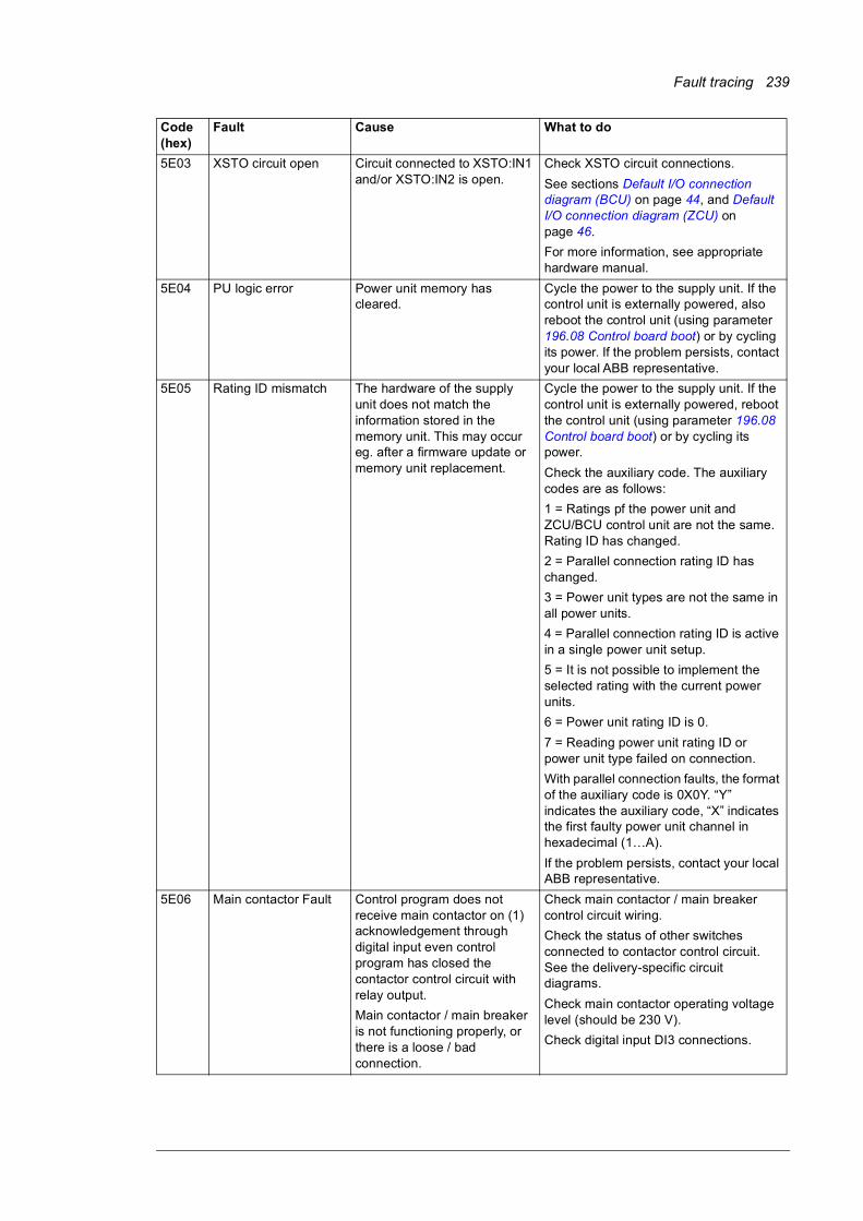
Fault tracing 239
5E03 XSTO circuit open Circuit connected to XSTO:IN1 and/or XSTO:IN2 is open.
Check XSTO circuit connections.
See sections Default I/O connection diagram (BCU) on page 44, and Default I/O connection diagram (ZCU) on page 46.
For more information, see appropriate hardware manual.
5E04 PU logic error Power unit memory has cleared.
Cycle the power to the supply unit. If the control unit is externally powered, also reboot the control unit (using parameter 196.08 Control board boot) or by cycling its power. If the problem persists, contact your local ABB representative.
5E05 Rating ID mismatch The hardware of the supply unit does not match the information stored in the memory unit. This may occur eg. after a firmware update or memory unit replacement.
Cycle the power to the supply unit. If the control unit is externally powered, reboot the control unit (using parameter 196.08 Control board boot) or by cycling its power.
Check the auxiliary code. The auxiliary codes are as follows:
1 = Ratings pf the power unit and ZCU/BCU control unit are not the same. Rating ID has changed.
2 = Parallel connection rating ID has changed.
3 = Power unit types are not the same in all power units.
4 = Parallel connection rating ID is active in a single power unit setup.
5 = It is not possible to implement the selected rating with the current power units.
6 = Power unit rating ID is 0.
7 = Reading power unit rating ID or power unit type failed on connection.
With parallel connection faults, the format of the auxiliary code is 0X0Y. “Y” indicates the auxiliary code, “X” indicates the first faulty power unit channel in hexadecimal (1…A).
If the problem persists, contact your local ABB representative.
5E06 Main contactor Fault Control program does not receive main contactor on (1) acknowledgement through digital input even control program has closed the contactor control circuit with relay output.
Main contactor / main breaker is not functioning properly, or there is a loose / bad connection.
Check main contactor / main breaker control circuit wiring.
Check the status of other switches connected to contactor control circuit. See the delivery-specific circuit diagrams.
Check main contactor operating voltage level (should be 230 V).
Check digital input DI3 connections.
Code (hex)
Fault Cause What to do
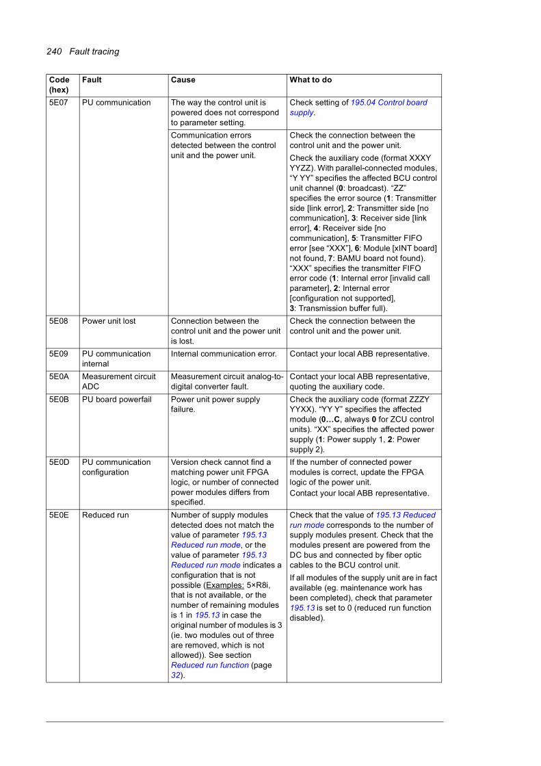
240 Fault tracing
5E07 PU communication The way the control unit is powered does not correspond to parameter setting.
Check setting of 195.04 Control board supply.
Communication errors detected between the control unit and the power unit.
Check the connection between the control unit and the power unit.
Check the auxiliary code (format XXXY YYZZ). With parallel-connected modules, “Y YY” specifies the affected BCU control unit channel (0: broadcast). “ZZ” specifies the error source (1: Transmitter side [link error], 2: Transmitter side [no communication], 3: Receiver side [link error], 4: Receiver side [no communication], 5: Transmitter FIFO error [see “XXX”], 6: Module [xINT board] not found, 7: BAMU board not found). “XXX” specifies the transmitter FIFO error code (1: Internal error [invalid call parameter], 2: Internal error [configuration not supported], 3: Transmission buffer full).
5E08 Power unit lost Connection between the control unit and the power unit is lost.
Check the connection between the control unit and the power unit.
5E09 PU communication internal
Internal communication error. Contact your local ABB representative.
5E0A Measurement circuit ADC
Measurement circuit analog-to-digital converter fault.
Contact your local ABB representative, quoting the auxiliary code.
5E0B PU board powerfail Power unit power supply failure.
Check the auxiliary code (format ZZZY YYXX). “YY Y” specifies the affected module (0…C, always 0 for ZCU control units). “XX” specifies the affected power supply (1: Power supply 1, 2: Power supply 2).
5E0D PU communication configuration
Version check cannot find a matching power unit FPGA logic, or number of connected power modules differs from specified.
If the number of connected power modules is correct, update the FPGA logic of the power unit.Contact your local ABB representative.
5E0E Reduced run Number of supply modules detected does not match the value of parameter 195.13 Reduced run mode, or the value of parameter 195.13 Reduced run mode indicates a configuration that is not possible (Examples: 5×R8i, that is not available, or the number of remaining modules is 1 in 195.13 in case the original number of modules is 3 (ie. two modules out of three are removed, which is not allowed)). See section Reduced run function (page 32).
Check that the value of 195.13 Reduced run mode corresponds to the number of supply modules present. Check that the modules present are powered from the DC bus and connected by fiber optic cables to the BCU control unit.
If all modules of the supply unit are in fact available (eg. maintenance work has been completed), check that parameter 195.13 is set to 0 (reduced run function disabled).
Code (hex)
Fault Cause What to do

Fault tracing 241
5E0F PU state feedback State feedback from output phases does not match control signals.
Contact your local ABB representative.
5E10 Charging feedback Charging feedback signal missing.
Check the feedback signal coming from the charging system.
Incorrect parameter setting Check the setting of parameter 195.09 Switch fuse controller. Enable the parameter only if an xSFC charging controller is installed.
The charging switch and DC switch were operated out of sequence, or a start command was issued before the unit was ready.
The normal power-up sequence is:1. Close charging switch.
2. After charging finishes (charging OK lamp lights), close DC switch.
3. Open charging switch.
5E11 Unknown PU fault Unidentified power unit logic fault.
Check the logic and firmware compatibility.
Contact your local ABB representative.
5E13 Auxiliary Circuit breaker
Circuit breaker fault trigged by input selected with parameter 131.32 Aux circuit breaker fault source
By default, the feedback is connected to DI4.
5E18 Charge contactor Supply voltage is removed while the drive is running.
Reconnect the supply voltage.
5E14 Measurement circuit temperature
Problem with internal temperature measurement of the drive.
See AE19 Measurement circuit temperature (page 227).
6E00 FPGA version incompatible
Firmware and FPGA versions are incompatible.
Update power unit FPGA logic or firmware (whichever is older).Reboot the control unit (using parameter 196.08 Control board boot) or by cycling power. If the problem persists, contact your local ABB representative.
6E01 FBA A mapping file Fieldbus adapter A mapping file read error.
Contact your local ABB representative.
6E02 FBA B mapping file Fieldbus adapter B mapping file read error.
Contact your local ABB representative.
6E03 Task overload Internal fault. Reboot the control unit (using parameter 196.08 Control board boot) or by cycling power. If the problem persists, contact your local ABB representative.
6E04 Stack overflow Internal fault. Reboot the control unit (using parameter 196.08 Control board boot) or by cycling power. If the problem persists, contact your local ABB representative.
6E05 Internal file load File read error. Reboot the control unit (using parameter 196.08 Control board boot) or by cycling power. If the problem persists, contact your local ABB representative.
6E06 Internal record load Internal record load error. Contact your local ABB representative.
6E07 Application loading Application file incompatible or corrupted.
Check the auxiliary code. See actions for each code below.
Code (hex)
Fault Cause What to do
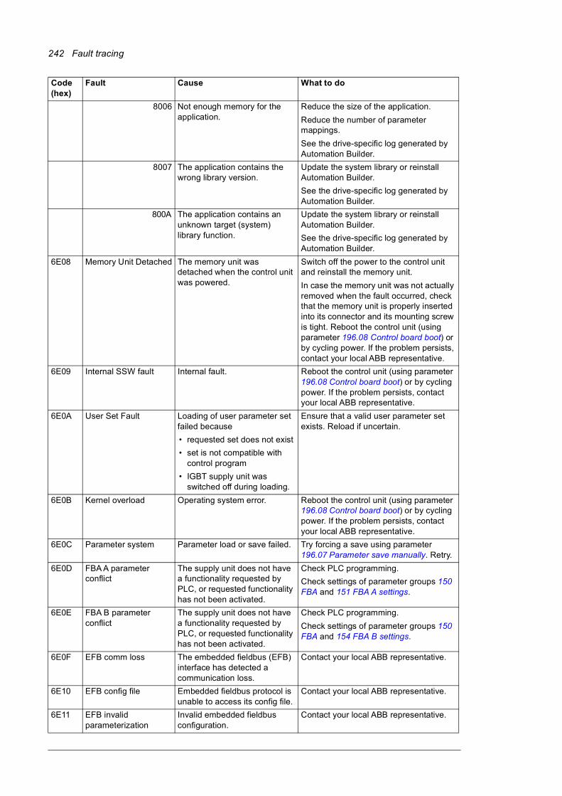
242 Fault tracing
8006 Not enough memory for the application.
Reduce the size of the application.
Reduce the number of parameter mappings.
See the drive-specific log generated by Automation Builder.
8007 The application contains the wrong library version.
Update the system library or reinstall Automation Builder.
See the drive-specific log generated by Automation Builder.
800A The application contains an unknown target (system) library function.
Update the system library or reinstall Automation Builder.
See the drive-specific log generated by Automation Builder.
6E08 Memory Unit Detached The memory unit was detached when the control unit was powered.
Switch off the power to the control unit and reinstall the memory unit.
In case the memory unit was not actually removed when the fault occurred, check that the memory unit is properly inserted into its connector and its mounting screw is tight. Reboot the control unit (using parameter 196.08 Control board boot) or by cycling power. If the problem persists, contact your local ABB representative.
6E09 Internal SSW fault Internal fault. Reboot the control unit (using parameter 196.08 Control board boot) or by cycling power. If the problem persists, contact your local ABB representative.
6E0A User Set Fault Loading of user parameter set failed because
• requested set does not exist
• set is not compatible with control program
• IGBT supply unit was switched off during loading.
Ensure that a valid user parameter set exists. Reload if uncertain.
6E0B Kernel overload Operating system error. Reboot the control unit (using parameter 196.08 Control board boot) or by cycling power. If the problem persists, contact your local ABB representative.
6E0C Parameter system Parameter load or save failed. Try forcing a save using parameter 196.07 Parameter save manually. Retry.
6E0D FBA A parameter conflict
The supply unit does not have a functionality requested by PLC, or requested functionality has not been activated.
Check PLC programming.
Check settings of parameter groups 150 FBA and 151 FBA A settings.
6E0E FBA B parameter conflict
The supply unit does not have a functionality requested by PLC, or requested functionality has not been activated.
Check PLC programming.
Check settings of parameter groups 150 FBA and 154 FBA B settings.
6E0F EFB comm loss The embedded fieldbus (EFB) interface has detected a communication loss.
Contact your local ABB representative.
6E10 EFB config file Embedded fieldbus protocol is unable to access its config file.
Contact your local ABB representative.
6E11 EFB invalid parameterization
Invalid embedded fieldbus configuration.
Contact your local ABB representative.
Code (hex)
Fault Cause What to do

Fault tracing 243
6E12 EFB load fault Unable to load protocol firmware or version mismatch between protocol and system firmware.
Contact your local ABB representative.
6E15 Text data overflow Internal fault. Reset the fault. Contact your local ABB representative if the fault persists.
6E16 Text 32-bit table overflow
Internal fault. Reset the fault. Contact your local ABB representative if the fault persists.
6E17 Text 64-bit table overflow
Internal fault. Reset the fault. Contact your local ABB representative if the fault persists.
6E18 Text file overflow Internal fault. Reset the fault. Contact your local ABB representative if the fault persists.
6E19 Synchronization fault Synchronization to supply network has failed.
Monitor possible network transients.
6E1A Rating ID fault Rating ID load error. Contact your local ABB representative.
6E1B Backup/Restore Timeout
A control panel or PC tool fails to communicate with the drive during backup or restoring operation.
Check the control panel or PC tool communication, and if it is still in backup/restore state.
6E1C Emergency stop fault Drive has received an emergency stop command.
Check that it is safe to continue operation.
Return the emergency stop pushbutton to normal position.
Restart the drive.
6E1D Internal SW error Internal error. Contact your local ABB representative. Quote the auxiliary code (check the event details in the event log).
6E1E Unrecoverable SW error
An unrecoverable error has occurred.
Record the fault code and the auxiliary fault code and report them to your local ABB representative.
Cycle power to the unit to recover.
6E1F Licensing fault There are two types of licenses being used in ACS880 drives: licenses that need to be found from the unit which allow the firmware to be executed, and licenses that prevent the firmware from running.The license is indicated by the value of the auxiliary code field. The license is Nxxxx, where xxxx is indicated by the 4-digit value of the auxiliary code field.
Record the auxiliary codes of all active licensing faults and contact your product vendor for further instructions.
This fault requires a reboot of the control unit either by switching the power off and on, or using parameter 196.08 Control board boot.
8201 A restrictive license is found from the unit. The firmware on this supply unit cannot be executed because a Low harmonic license is found from the unit. This unit is meant to be used with IGBT supply control program (2Q) only.
Contact your product vendor for further instructions.
6E20 Fault reset Fault reset has been requested and done.
Informative fault.
Code (hex)
Fault Cause What to do
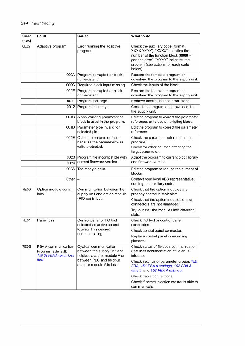
244 Fault tracing
6E27 Adaptive program Error running the adaptive program.
Check the auxiliary code (format XXXX YYYY). “XXXX” specifies the number of the function block (0000 = generic error). “YYYY” indicates the problem (see actions for each code below).
000A Program corrupted or block non-existent
Restore the template program or download the program to the supply unit.
000C Required block input missing Check the inputs of the block.
000E Program corrupted or block non-existent
Restore the template program or download the program to the supply unit.
0011 Program too large. Remove blocks until the error stops.
0012 Program is empty. Correct the program and download it to the supply unit.
001C A non-existing parameter or block is used in the program.
Edit the program to correct the parameter reference, or to use an existing block.
001D Parameter type invalid for selected pin.
Edit the program to correct the parameter reference.
001E Output to parameter failed because the parameter was write-protected.
Check the parameter reference in the program.Check for other sources affecting the target parameter.
0023 Program file incompatible with current firmware version.
Adapt the program to current block library and firmware version.0024
002A Too many blocks. Edit the program to reduce the number of blocks.
Other – Contact your local ABB representative, quoting the auxiliary code.
7E00 Option module comm loss
Communication between the supply unit and option module (FIO-xx) is lost.
Check that the option modules are properly seated in their slots.
Check that the option modules or slot connectors are not damaged.
Try to install the modules into different slots.
7E01 Panel loss Control panel or PC tool selected as active control location has ceased communicating.
Check PC tool or control panel connection.
Check control panel connector.
Replace control panel in mounting platform.
7E0B FBA A communicationProgrammable fault: 150.02 FBA A comm loss func
Cyclical communication between the supply unit and fieldbus adapter module A or between PLC and fieldbus adapter module A is lost.
Check status of fieldbus communication. See user documentation of fieldbus interface.
Check settings of parameter groups 150 FBA, 151 FBA A settings, 152 FBA A data in and 153 FBA A data out.
Check cable connections.
Check if communication master is able to communicate.
Code (hex)
Fault Cause What to do
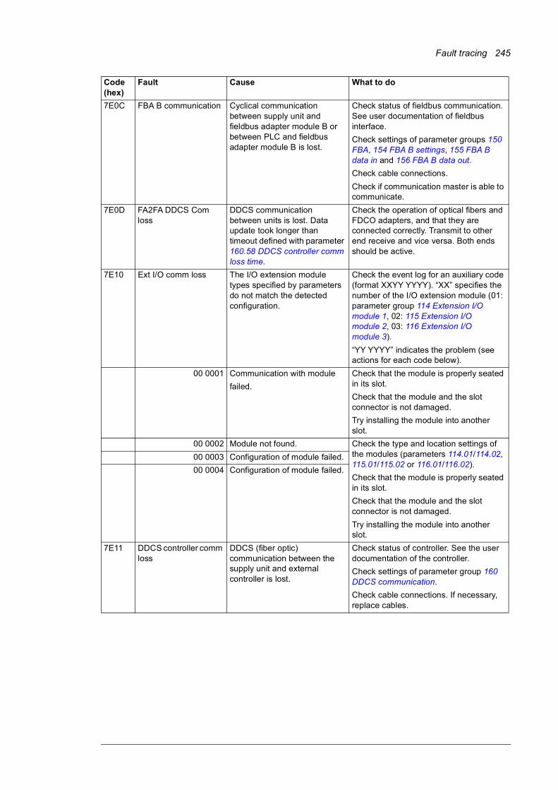
Fault tracing 245
7E0C FBA B communication Cyclical communication between supply unit and fieldbus adapter module B or between PLC and fieldbus adapter module B is lost.
Check status of fieldbus communication. See user documentation of fieldbus interface.
Check settings of parameter groups 150 FBA, 154 FBA B settings, 155 FBA B data in and 156 FBA B data out.
Check cable connections.
Check if communication master is able to communicate.
7E0D FA2FA DDCS Com loss
DDCS communication between units is lost. Data update took longer than timeout defined with parameter 160.58 DDCS controller comm loss time.
Check the operation of optical fibers and FDCO adapters, and that they are connected correctly. Transmit to other end receive and vice versa. Both ends should be active.
7E10 Ext I/O comm loss The I/O extension module types specified by parameters do not match the detected configuration.
Check the event log for an auxiliary code (format XXYY YYYY). “XX” specifies the number of the I/O extension module (01: parameter group 114 Extension I/O module 1, 02: 115 Extension I/O module 2, 03: 116 Extension I/O module 3).
“YY YYYY” indicates the problem (see actions for each code below).
00 0001 Communication with module
failed.
Check that the module is properly seated in its slot.
Check that the module and the slot connector is not damaged.
Try installing the module into another slot.
00 0002 Module not found. Check the type and location settings of the modules (parameters 114.01/114.02, 115.01/115.02 or 116.01/116.02).
Check that the module is properly seated in its slot.
Check that the module and the slot connector is not damaged.
Try installing the module into another slot.
00 0003 Configuration of module failed.
00 0004 Configuration of module failed.
7E11 DDCS controller comm loss
DDCS (fiber optic) communication between the supply unit and external controller is lost.
Check status of controller. See the user documentation of the controller.
Check settings of parameter group 160 DDCS communication.
Check cable connections. If necessary, replace cables.
Code (hex)
Fault Cause What to do

246 Fault tracing
8E06 AI supervision An analog signal is outside the limits specified for the analog input.
Check the event log for an auxiliary code (format XXXX XYZZ). “Y” specifies the location of the input (0: Control unit, 1: I/O extension module 1, 2: I/O extension module 2, 3: I/O extension module 3). “ZZ” specifies the limit (01: AI1 under minimum, 02: AI1 above maximum, 03: AI2 under minimum, 04: AI2 above maximum).Check signal level at the analog input.Check the wiring connected to the input.Check the minimum and maximum limits of the input in parameter group 112 Standard AI.
8E07 Net lost Net lost is detected. Duration of net lost is too long.
Resynchronize the IGBT supply unit to the grid after net lost.
9E01 External fault 1(Editable message text)Programmable fault: 131.01 External event 1 source131.02 External event 1 type
Fault in external device 1. (This information is configured through one of programmable digital inputs.)
Check external devices for faults.
Check the setting of parameter 131.01 External event 1 source.
9E02 External fault 2(Editable message text)Programmable fault: 131.03 External event 2 source131.04 External event 2 type
Fault in external device 2. (This information is configured through one of programmable digital inputs.)
Check external devices for faults.
Check the setting of parameter 131.03 External event 2 source.
9E03 External fault 3(Editable message text)Programmable fault: 131.05 External event 3 source131.06 External event 3 type
Fault in external device 3. (This information is configured through one of programmable digital inputs.)
Check external devices for faults.
Check the setting of parameter 131.05 External event 3 source.
9E04 External fault 4(Editable message text)Programmable fault: 131.07 External event 4 source131.08 External event 4 type
Fault in external device 4. (This information is configured through one of programmable digital inputs.)
Check external devices for faults.
Check the setting of parameter 131.07 External event 4 source.
9E05 External fault 5(Editable message text)Programmable fault: 131.09 External event 5 source131.10 External event 5 type
Fault in external device 5. (This information is configured through one of programmable digital inputs.)
Check external devices for faults.
Check the setting of parameter 131.09 External event 5 source.
FE06 MF communication lossProgrammable fault: 160.09 M/F comm loss function
Master/follower communication is lost.
See AE81 MF comm loss (page 232).
FE07 Follower drive failureProgrammable fault: 160.17 Follower fault action
A follower has tripped. Check the auxiliary code. Add 2 to the code to find out the node address of the faulted unit.
Correct the fault in the follower.
Code (hex)
Fault Cause What to do

Fault tracing 247
FF81 FB A force trip A fault trip command has been received through fieldbus adapter A.
Check the fault information provided by the PLC.
FF82 FB B force trip A fault trip command has been received through fieldbus adapter B.
Check the fault information provided by the PLC.
FF8E EFB force trip A fault trip command has been received through the embedded fieldbus interface.
Contact your local ABB representative.
Code (hex)
Fault Cause What to do

248 Fault tracing

Fieldbus control through the embedded fieldbus interface (EFB) 249
9
Fieldbus control through the embedded fieldbus interface (EFB)
This feature is not supported by the current firmware version.

250 Fieldbus control through the embedded fieldbus interface (EFB)

Fieldbus control through a fieldbus adapter 251
10
Fieldbus control through a fieldbus adapter
What this chapter containsThis chapter describes how the IGBT supply unit can be controlled by external devices over a communication network (fieldbus) through an optional fieldbus adapter module.

252 Fieldbus control through a fieldbus adapter
System overviewThe user can control the IGBT supply unit through a fieldbus interface if the unit is equipped with an optional fieldbus adapter (for example, option +K454). Then the supply unit can be connected to an external control system through a serial communication link. The fieldbus adapter can be installed into any free option slot of the control unit.
The supply unit can be set to receive all of its control information through the fieldbus interface, or the control can be distributed between the fieldbus interface and other available sources such as digital and analog inputs.
Fieldbus adapters are available for various serial communication systems and protocols, for example• CANopen (FCAN-01 adapter)
• ControlNet (FCNA-01 adapter)
• DeviceNet (FDNA-01 adapter)
• EtherCAT (FECA-01 adapter)
• EtherNet/IP (FENA-11, FENA-21 or FEIP-21 adapter)
• Modbus/RTU (FSCA-01 adapter)
• Modbus TCP (FENA-11, FENA-21 or FMBT-21 adapter)
• POWERLINK (FEPL-02 adapter)
• PROFIBUS DP (FPBA-01 adapter)
• PROFINET IO (FENA-11, FENA-21 or FPNO-21 adapter).
Note: The text and examples in this chapter describe the configuration of one fieldbus adapter (FBA A) by parameters 150.01…150.21 and parameter groups 151…153. The second adapter (FBA B), if present, is configured in a similar fashion by parameters 150.31…150.51 and parameter groups 154…156.
Data Flow
Process I/O (cyclic)
Process I/O (cyclic) or Service messages (acyclic)
Control word (CW)
References
Fieldbus controller
Parameter R/W requests/responses
Status word (SW)
Actual values
Fieldbus
Other devices
ACS880
Type Fxxx fieldbus adapter installed on the control unit

Fieldbus control through a fieldbus adapter 253
Note: If FENA-xx Ethernet adapter is used for Ethernet tool network and Drive composer PC tool, use the FENA-xx adapter as fieldbus adapter B. Configure the FENA-xx adapter through parameters 150.31…150.51 and parameter groups 154…156. Normally, use the fieldbus adapter module as fieldbus adapter A. See Ethernet tool network for ACS880 drives application guide (3AUA0000125635 [English]), and FENA-01/-11 Ethernet adapter module user’s manual (3AUA0000093568 [English]).
Basics of the fieldbus control interfaceThe cyclic communication between a fieldbus system and the IGBT supply unit consists of 16/32-bit input and output data words. The supply unit supports at the maximum the use of 12 data words (16 bits) in each direction.
Data transmitted from the IGBT supply unit to the fieldbus controller is defined by parameters 152.01 FBA A data in1 … 152.12 FBA A data in12. The data transmitted from the fieldbus controller to the IGBT supply unit is defined by parameters 153.01 FBA data out1 … 153.12 FBA data out12.
Control word and Status word
The Control word is the principal means for controlling the IGBT supply unit from a fieldbus system. It is sent by the fieldbus master station to the IGBT supply unit through the adapter module. The IGBT supply unit switches between its states according to the bit-coded instructions on the Control word, and returns status information to the master in the Status word.
The contents of the Control word and the Status word are detailed on pages 256 and 257 respectively.
If parameter 150.12 FBA A debug mode is set to Fast, the Control word received from the fieldbus is shown by parameter 150.13 FBA A control word, and the Status word transmitted to the fieldbus network by 150.16 FBA A status word.
References
References are 16-bit words containing a sign bit and a 15-bit integer. A negative reference is formed by calculating the two’s complement from the corresponding positive reference.
ABB drives can receive control information from multiple sources including analogue and digital inputs, the control panel and a fieldbus adapter module. In order to have the IGBT supply unit controlled through the fieldbus, the module must be defined as the source for control information, e.g. Reference.
If parameter 150.12 FBA A debug mode is set to Fast, the references received from the fieldbus are displayed by 150.14 FBA A reference 1 and 150.15 FBA A reference 2.
Scaling of references
Note: The scalings described below are for the Transparent 16 profile. Fieldbus-specific communication profiles may use different scalings. For more information, see the manual of the fieldbus adapter.
The references are scaled as defined by parameters 146.01…146.04.
Example: PLC reference is 600. Parameter 152.02 FBA A data in1 is set to Ref1 16bit. Reference Ref1/Act1 is scaled first by parameter 151.06 T16 scale since the supply units are identified automatically as Transparent 16 profile. After that the value is scaled in

254 Fieldbus control through a fieldbus adapter
parameter group 146 Monitoring settings, for example using parameter 146.01 Power scaling.
Example for PROFIBUS:
146.04 DC voltage scaling is set to 1000,151.06 T16 scale is set to 99, which equals to coefficient 100. 0 equals to coefficient 1.PLC reference is 105.
Scaled value is calculated as follows:
105 [PLC reference] × 100 [T16 scale] × (1000 [par. 146.04] / 10000) = 1050 V.
Since the value is in 16-bit format and if the reference is 900, parameter 151.06 T16 scale causes the value to be 90000. This causes overflow. Then parameter 151.06 T16 scale needs to be changed first to zero, before reference 900 is possible.
Parameter 151.06 T16 scale is in use only in some of the fieldbus adapters and only for Ref1/Act1. For more information, see the manual of the fieldbus adapter.
Actual values
Actual values are 16-bit words containing information on the operation of the IGBT supply unit. The types of the monitored signals are selected by parameters 150.07 FBA A actual1 type and 150.08 FBA A actual2 type.
If parameter 150.12 FBA A debug mode is set to Fast, the actual values sent to the fieldbus are displayed by 150.17 FBA A actual value 1 and 150.18 FBA A actual value 2.

Fieldbus control through a fieldbus adapter 255
Fieldbus scaling diagram
The diagram below shows the fieldbus scaling principle.
Fieldbus module
Control board
Only in some fieldbus adapters
Only in CANopen and CyberSecCANopen Only when par. 150.04
is set to General.
Only when par. 150.04 is set to DC Voltage or Voltage or Power.
Notes:
• Division by 100 is done only with General type. Multiplication by P146.0x/10000 only with DC voltage or Active power types.
• In P146.0x, x can be:
• (146.01) 1 = Power scaling when Operation mode is Power control
• (146.04) 4 = DC voltage scaling when Operation mode is DC control

256 Fieldbus control through a fieldbus adapter
Contents of the fieldbus Control word
Bit Name Value Description
0 On/Off 1 Start charging.
Note: This bit affects only in external charge mode, ie. when the parameter 120.30 External charge enable is set to Yes. In internal change mode charging is handled automatically.
0 Open main contactor (switch power off).
1 Off 2 1 Emergency stop bit 2
0 Open main contactor
2 Off 3 1 Emergency stop bit 3
0 Open main contactor
3 Start 1 Start modulating.
0 Stop modulating.
4 - 1 Not in use
0 Not in use
5 - 1 Not in use
0 Not in use
6 - 1 Not in use
0 Not in use
7 Reset 1 Fault reset (0 -> 1) if an active fault exists. Enter switch-on inhibited.
0 Continue normal operation.
8 - 1 Not in use
0 Not in use
9 - 1 Not in use
0 Not in use
10 Remote cmd 1 Control location: REMOTE (EXT1 or EXT2).
0 Control location: LOCAL.
11 Ext ctrl loc 1 Select External Control Location EXT2. Effective if control location is parameterized to be selected from fieldbus.
0 Select External Control Location EXT1. Effective if control location is parameterized to be selected from fieldbus.
12 User bit 0 1 User bit 0 from external control location.
0 User bit 0 from external control location.
13 User bit 1 1 User bit 1 from external control location.
0 User bit 1 from external control location.
14 User bit 2 1 User bit 2 from external control location.
0 User bit 2 from external control location.
15 User bit 3 1 User bit 3 from external control location.
0 User bit 3 from external control location.

Fieldbus control through a fieldbus adapter 257
Contents of the fieldbus Status word
Bit Name Value Description
0 Ready to switch ON
1 Ready to switch on.
0 Not ready to switch on.
1 Ready run 1 Ready to operate, DC link charged.
0 Not ready to operate, DC link not charged.
2 Ready ref 1 Operation enabled.
0 Operation inhibited.
3 Tripped 1 Fault
0 No fault
4 - 1 Not in use
0 Not in use
5 - 1 Not in use
0 Not in use
6 - 1 Not in use
0 Not in use
7 Warning 1 Warning active.
0 No warning active.
8 Modulating 1 Converter is modulating.
0 Converter is not modulating.
9 Remote 1 Supply unit control location: REMOTE (EXT1 or EXT2).
0 Supply unit control location: LOCAL.
10 Net OK 1 Network voltage is OK (Ready ref = operation is enabled).
0 Network voltage is lost (Ready ref = operation is inhibited).
11 User bit 0 1 See parameter 106.30 MSW bit 11 sel.
0 See parameter 106.30 MSW bit 11 sel.
12 User bit 1 1 See parameter 106.31 MSW bit 12 sel.
0 See parameter 106.31 MSW bit 12 sel.
13 User bit 2 1 See parameter 106.32 MSW bit 13 sel.
0 See parameter 106.32 MSW bit 13 sel.
14 Charging 1 Charging contactor closed.
0 Charging contactor open.
15 User bit 3 1 See parameter 106.33 MSW bit 15 sel.
0 See parameter 106.33 MSW bit 15 sel.
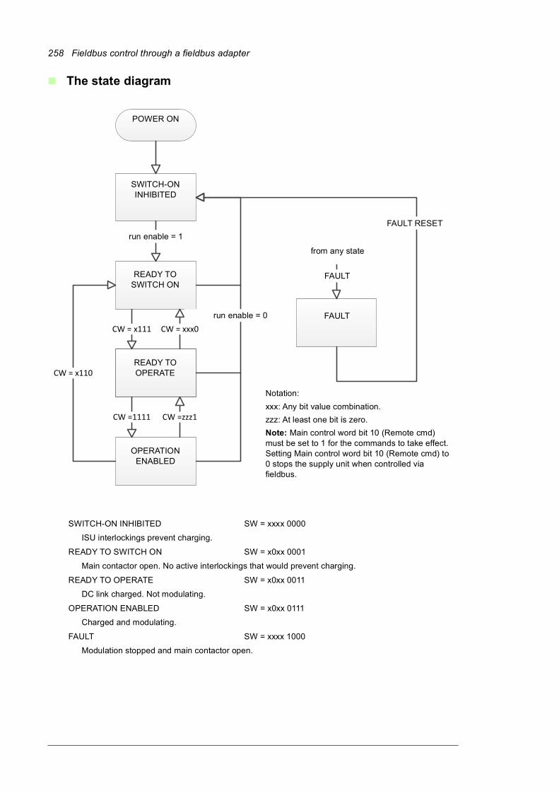
258 Fieldbus control through a fieldbus adapter
The state diagram
READY TOOPERATE
CW =zzz1CW =1111
CW = xxx0CW = x111
CW = x110
POWER ON
SWITCH-ON INHIBITED
READY TO SWITCH ON
READY TO OPERATE
OPERATION ENABLED
FAULT
from any state
Notation:
xxx: Any bit value combination.
zzz: At least one bit is zero.
Note: Main control word bit 10 (Remote cmd) must be set to 1 for the commands to take effect. Setting Main control word bit 10 (Remote cmd) to 0 stops the supply unit when controlled via fieldbus.
SWITCH-ON INHIBITED SW = xxxx 0000
ISU interlockings prevent charging.
READY TO SWITCH ON SW = x0xx 0001
Main contactor open. No active interlockings that would prevent charging.
READY TO OPERATE SW = x0xx 0011
DC link charged. Not modulating.
OPERATION ENABLED SW = x0xx 0111
Charged and modulating.
FAULT SW = xxxx 1000
Modulation stopped and main contactor open.
run enable = 1
FAULT
FAULT RESET
run enable = 0

Fieldbus control through a fieldbus adapter 259
Setting up the IGBT supply unit for fieldbus controlBefore configuring the IGBT supply unit for fieldbus control, the adapter module must be mechanically and electrically installed according to the instructions given in the user’s manual of the appropriate fieldbus adapter module.
Note: To be able to switch the main contactor and the IGBT supply unit on and off through the fieldbus, the Run enable command at the digital input DI2 (by default) must be on (1).
1. Power up the IGBT supply unit.
2. Enable the communication between the IGBT supply unit and the fieldbus adapter module by setting the parameter 150.01 FBA A enable.
3. With 150.02 FBA A comm loss func, select how the IGBT supply unit should react to a fieldbus communication break.Note: This function monitors both the communication between the fieldbus master and the adapter module and the communication between the adapter module and the IGBT supply unit.
4. With 150.03 FBA A comm loss t out, define the time between communication break detection and the selected action.
5. Select application-specific values for the rest of the parameters in group 150 FBA.
6. Set the fieldbus adapter module configuration parameters in group 151 FBA A settings. At the minimum, set the required node address and the communication profile. Set profile to transparent 16 mode. Note: The parameter indexes and names vary as the way the different fieldbus adapters use these parameters. Example: For the FPBA adapter, set parameter 151.05 Profile to mode Trans16.
7. Define the process data transferred to and from the IGBT supply unit in parameter groups 152 FBA A data in and 153 FBA A data out.Note: The adapter module sets the Status word and Control word automatically into parameters 152.01 and 153.01 respectively.
8. Save the valid parameter values to permanent memory by setting parameter 196.07 Parameter save manually to Save.
9. Validate the settings made in parameter groups 151, 152 and 153 by setting parameter 151.27 FBA A par refresh to Configure.
10. Select the fieldbus adapter A as the source of the start and stop commands for external control location EXT1 by setting parameter 120.01 Ext1 commands to Fieldbus A.
11. Set the relevant control parameters to control the IGBT supply unit according to the application.

260 Fieldbus control through a fieldbus adapter
Setting up communication through inverter unitCommunication port is selected with parameter 60.71 INU-LSU communication port in inverter unit and with parameter 160.51 DDCS controller comm port in IGBT supply unit. Connect fiber optic cables between inverter unit and IGBT supply unit. Typically RDCO CH1 is used in inverter unit and RDCO CH0 is used in IGBT supply unit when BCU-x2 control unit is in use. When ZCU control unit is used, eg. channel A on FDCO module in slot 3 is used in IGBT supply unit. Setting the parameter 195.20 HW options word 1 bit 11 to Yes automatically sets all the communication parameters to their right values.
Set the parameters as follows:
In IGBT supply unit, data transmitted from the IGBT supply unit is defined with parameters 161.51 Data set 11 data 1 selection…161.53 Data set 11 data 3 selection. Data is received using parameters 162.51 Data set 10 data 1 selection…162.53 Data set 10 data 3 selection.
In inverter unit, data transmitted to the IGBT supply unit is defined with parameters 61.151…61.153. Data is received using parameters 62.151…62.153.
IGBT supply unit parameter Setting
120.01 Ext1 commands DDCS controller
120.02 Ext1 start trigger type Level
160.58 DDCS controller comm loss time Set time, eg. 4 ms.
160.51 DDCS controller comm port Set port to be used. Eg, slot 3A is used with ZCU control unit, and RDCO CH0 is used with BCU-x2 control unit.
161.51 Data set 11 data 1 selection SW 16bit
162.51 Data set 10 data 1 selection CW 16bit
Inverter unit parameter Setting
94.01 LSU control On
60.71 INU-LSU communication port RDCO CH1
61.151 INU-LSU data set 10 data 1 sel LSU CW
62.151 INU-LSU data set 11 data 1 sel LSU SW

Drive-to-drive link 261
11
Drive-to-drive link
This feature is not supported by the current firmware version.

262 Drive-to-drive link
Control chain diagrams 263
12
Control chain diagrams
What this chapter containsThe chapter presents the control chain diagrams of the control program.
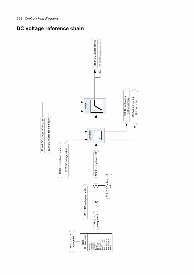
264 Control chain diagrams
DC voltage reference chain
123.
05 D
C v
olta
ge re
f 2+
123.
03 D
Cvo
ltage
ref 1
123.
01 U
ser D
Cvo
ltage
ref
x
123.
12 D
C v
olta
ge re
f sca
le
123.
13 D
C v
olta
ge re
fad
d
123.
11 D
C v
olta
ge re
f out
Lim
itatio
n
123.
06 D
C v
olta
ge re
f max
123.
07 D
C v
olta
ge re
f min
Ram
p
123.
09 D
C v
olta
ge re
f ram
p up
123.
10 D
C v
olta
ge re
f ram
p do
wn
123.
08 D
C v
olta
ge re
f lim
130.
04 L
imit
wor
d 4
bit 1
Udc
ref m
in
130.
04 L
imit
wor
d 4
bit 0
Udc
ref m
ax
Use
r ref
AI1
sca
led
AI2
sca
led
Pan
elFB
A re
f1FB
A re
f2D
DC
S c
trl re
f1D
DC
S c
trl re
f2M
/F re
f1 (B
CU
)M
/F re
f2 (B
CU
)O
ther
123.
02D
C v
olta
ge re
f sel

Control chain diagrams 265
Power reference chain
122.
03 P
ower
ref 1
Ipow
ref [
A]Ip
ow re
f [%
]Po
w re
f kW
Pow
ref %
122.
06Po
wer
ref t
ype
x12
2.04
Pow
er re
fsc
ale
Use
r ref
AI1
sca
led
AI2
sca
led
Pan
elFB
A re
f1FB
A re
f2D
DC
S c
trl re
f1D
DC
S c
trl re
f2M
/F re
f1 (B
CU
)M
/F re
f2 (B
CU
)O
ther
122.
02
Pow
er re
f sel
122.
08 Ip
ower
ref
122.
07 Ip
ower
ref %
122.
18 P
ower
ref o
ut %
122.
17 Ip
ower
ref o
ut
122.
01 U
ser P
ower
ref
122.
10 P
ower
ref
122.
09 P
ower
ref %
122.
19 P
ower
ref o
ut
122.
16 Ip
ower
ref o
ut %
Lim
itatio
n
122.
11 Ip
ower
ref m
ax %
122.
12 Ip
ower
ref m
in %
Ram
p
122.
14 Ip
ower
ref r
amp
up
122.
15 Ip
ower
ref r
amp
dow
n
122.
13 Ip
ower
ref l
im %
130.
01 L
imit
wor
d 1
bit 1
P u
ser r
ef m
in
130.
01 L
imit
wor
d 1
bit 0
P u
ser r
ef m
ax
122.
05P
ower
ref 2
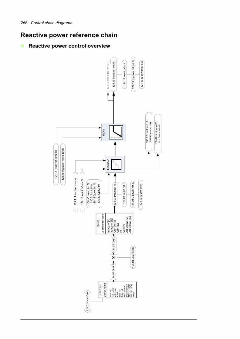
266 Control chain diagrams
Reactive power reference chain
Reactive power control overview
124.
03 Q
ref 1
Ireac
t ref
[A]
Ireac
t ref
[%]
Qre
f [kV
Ar]
Qre
f [%
]P
hiC
osP
hiAC
vol
t ref
[V]
AC v
olt r
ef [%
]
124.
06
Q p
ower
ref t
ype
124.
05 Q
ref 2
x
124.
04 Q
ref s
cale
Use
r ref
AI1
sca
led
AI2
sca
led
Pan
elFB
A re
f1FB
A re
f2D
DC
S c
trl re
f1D
DC
S c
trl re
f2M
/F re
f1 (B
CU
)M
/F re
f2 (B
CU
)O
ther12
4.02
Q
pow
er re
f sel
124.
08 Ir
eact
ref
124.
07 Ir
eact
ref %
124.
17 Ir
eact
ref o
ut
124.
18 Q
pow
er re
f out
%
124.
01 U
ser Q
ref
124.
09 Q
pow
er re
f %
124.
10 Q
pow
er re
f12
4.19
Q p
ower
ref o
ut
124.
16 Ir
eact
ref o
ut %
Lim
itatio
n
124.
11 Ir
eact
ref m
ax %
124.
12 Ir
eact
ref m
in %
Ram
p
124.
14 Ir
eact
ref r
amp
up
124.
15 Ir
eact
ref r
amp
dow
n
124.
13 Ir
eact
ref l
im %
130.
02 L
imit
wor
d 2
bit 1
Q u
ser r
ef m
in
130.
02 L
imit
wor
d 2
bit 0
Q u
ser r
ef m
ax
130.
30 Ir
eact
lim
%13
0.31
Irea
ct li
m13
0.32
Qpo
w li
m %
130.
33 Q
pow
lim
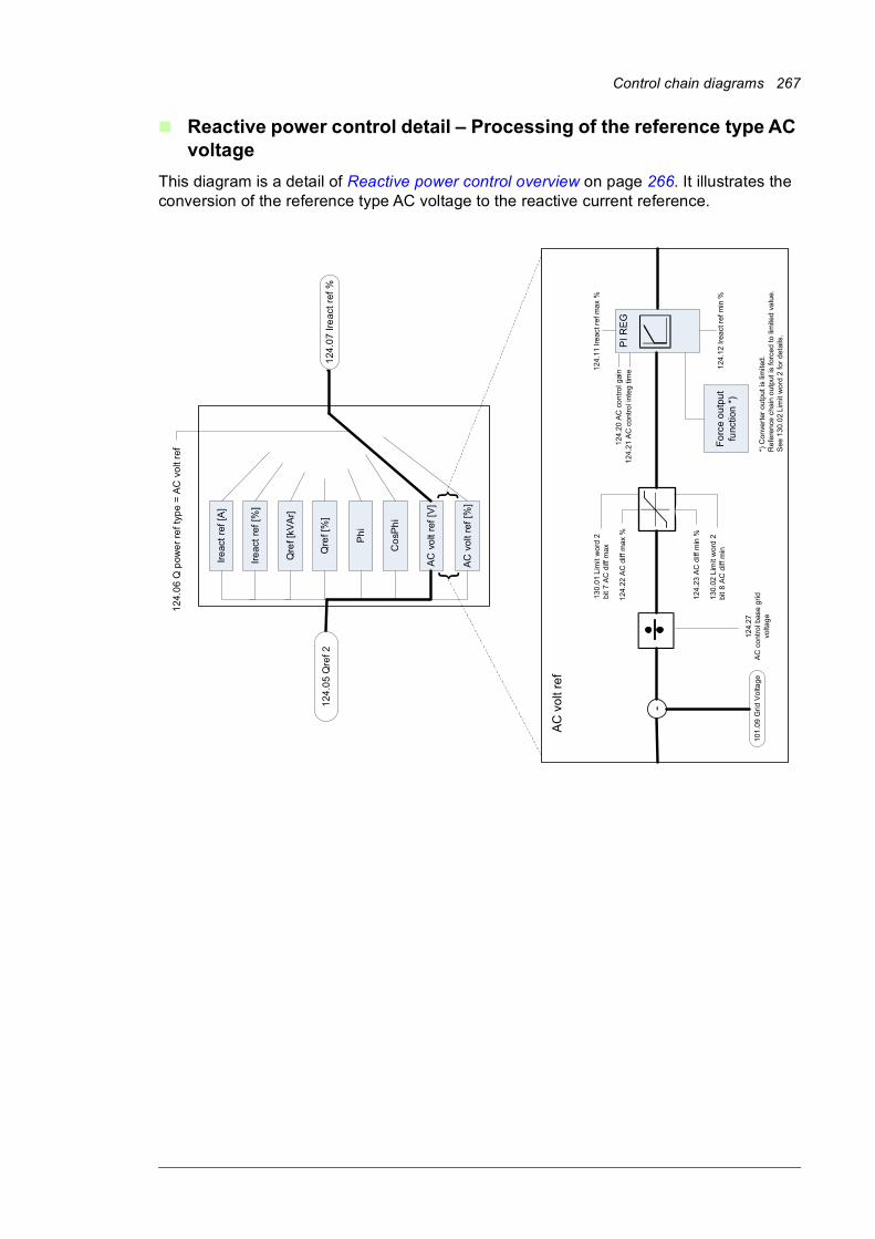
Control chain diagrams 267
Reactive power control detail – Processing of the reference type AC voltage
This diagram is a detail of Reactive power control overview on page 266. It illustrates the conversion of the reference type AC voltage to the reactive current reference.
Ireac
t ref
[A]
Ireac
t ref
[%]
Qre
f [kV
Ar]
Qre
f [%
]
Phi
Cos
Phi
AC
vol
t ref
[V]
124.
05 Q
ref 2
124.
06 Q
pow
er re
f typ
e =
AC v
olt r
ef
124.
07 Ir
eact
ref %
AC v
olt r
ef [%
]{
}
PI R
EG
101.
09 G
rid V
olta
ge
-
124.
22 A
C d
iff m
ax %
124.
23 A
C d
iff m
in %
AC
vol
t ref
124.
20 A
C c
ontro
l gai
n12
4.21
AC
con
trol i
nteg
tim
e124.
11 Ir
eact
ref m
ax %
124.
12 Ir
eact
ref m
in %
130.
01 L
imit
wor
d 2
bit 7
AC
diff
max
130.
02 L
imit
wor
d 2
bit 8
AC
diff
min
Forc
e ou
tput
func
tion
*)
*) C
onve
rter o
utpu
t is
limite
d.R
efer
ence
cha
in o
utpu
t is
forc
ed to
lim
ited
valu
e.S
ee 1
30.0
2 Li
mit
wor
d 2
for d
etai
ls.
124.
27A
C c
ontro
l bas
e gr
idvo
ltage
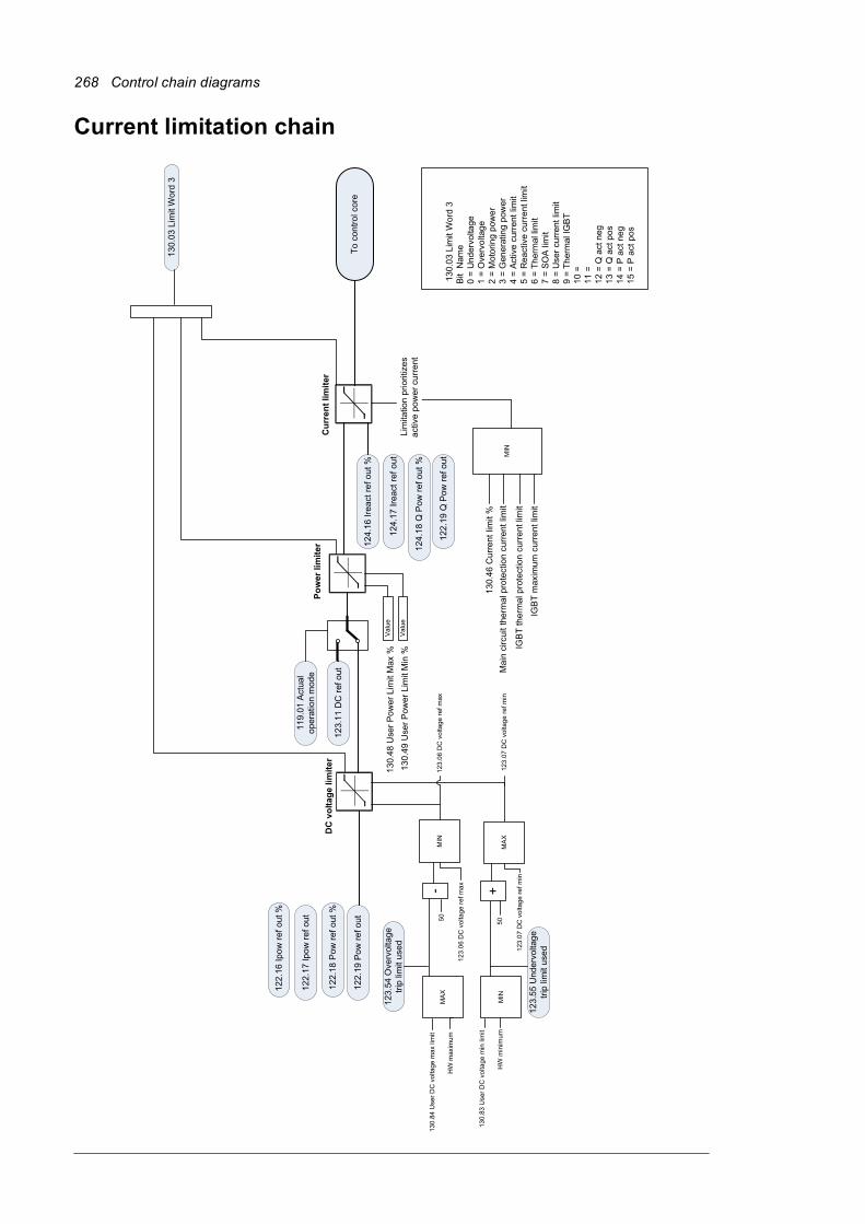
268 Control chain diagrams
Current limitation chain
To c
ontro
l cor
e
130
.03
Lim
it W
ord
3B
it N
ame
0 =
Und
ervo
ltage
1 =
Ove
rvol
tage
2 =
Mot
orin
g po
wer
3 =
Gen
erat
ing
pow
er4
= Ac
tive
curr
ent l
imit
5 =
Rea
ctiv
e cu
rren
t lim
it6
= Th
erm
al li
mit
7 =
SOA
lim
it8
= U
ser c
urre
nt li
mit
9 =
Ther
mal
IGB
T10
=11
=12
= Q
act
neg
13 =
Q a
ct p
os14
= P
act
neg
15 =
P a
ct p
os
Val
ue
Val
ue
Pow
er li
mite
r
130.
48 U
ser P
ower
Lim
it M
ax %
130.
49 U
ser P
ower
Lim
it M
in %
130.
03 L
imit
Wor
d 3
MIN
130.
46 C
urre
nt li
mit
%M
ain
circ
uit t
herm
al p
rote
ctio
n cu
rrent
lim
it
IGB
T th
erm
al p
rote
ctio
n cu
rren
t lim
it
IGB
T m
axim
um c
urre
nt li
mit
Cur
rent
lim
iter
DC
vol
tage
lim
iter
MA
X
123.
54 O
verv
olta
getri
p lim
it us
ed
123.
55 U
nder
volta
getri
p lim
it us
ed
MIN
130.
84 U
ser D
C v
olta
ge m
ax li
mit
HW
max
imum
130.
83 U
ser D
C v
olta
ge m
in li
mit
HW
min
imum
MIN
-50
123.
06 D
C v
olta
ge re
f max
MA
X
123.
07 D
C v
olta
ge re
f min
+50
123.
06 D
C v
olta
ge re
f max
123.
07 D
C v
olta
ge re
f min
123.
11 D
C re
f out
122.
16 Ip
ow re
f out
%
122.
17 Ip
ow re
f out
122.
18 P
ow re
f out
%
122.
19 P
ow re
f out
124.
16 Ir
eact
ref o
ut %
124.
17 Ir
eact
ref o
ut
124.
18 Q
Pow
ref o
ut %
122.
19 Q
Pow
ref o
ut
119.
01 A
ctua
lop
erat
ion
mod
e
Lim
itatio
n pr
iorit
izes
activ
e po
wer
cur
rent

—Further information
Product and service inquiriesAddress any inquiries about the product to your local ABB representative, quoting the type designation and serial number of the unit in question. A listing of ABB sales, support and service contacts can be found by navigating to abb.com/searchchannels.
Product trainingFor information on ABB product training, navigate to new.abb.com/service/training.
Providing feedback on ABB Drives manualsYour comments on our manuals are welcome. Navigate to new.abb.com/drives/manuals-feedback-form.
Document library on the InternetYou can find manuals and other product documents in PDF format on the Internet at abb.com/drives/documents.

abb.com/drives
3AU
A0
00
013
156
2 R
ev G
(E
N) 2
019
-11-
18
© Copyright 2019 ABB. All rights reserved.Specifications subject to change without notice.