emcp - kindlehk.com · to download a new firmware, the controller requires instruction sequence...
TRANSCRIPT

Rev A0
NCEPNA6M4-xxxx
www.longsys.com Longsys Electronics Page 1
eMCP
NCEPNA6M4-xxxx
Specification

Rev A0
NCEPNA6M4-xxxx
www.longsys.com Longsys Electronics Page 2
Document title
eMCP
eMMC(x8) Flash/ (x32) LPDDR3
Revision History
Revision No. History Draft Date Remark
A0 Initial Draft Jul 2017 Draft

Rev A0
NCEPNA6M4-xxxx
www.longsys.com Longsys Electronics Page 3
FEATURES [ eMCP ] ● Operation Temperature - (-25)oC ~ 70oC ● Package - 221-ball FBGA – 11.5x13.0mm2, 1.0t, 0.5mm pitch
[ eMMC ]
• eMMC5.0 compatible (Backward compatible to eMMC4.5) • Bus mode - Data bus width : 1-bit, 4-bit, 8-bit - Data transfer rate: up to 200MB/s (HS200) - MMC I/F Clock frequency : 0~200MHz • Operating voltage range - Vcc (NAND) : 2.7 - 3.6V - Vccq (Controller) : 1.7 - 1.95V / 2.7 - 3.6V • Temperature - Operation (-25℃ ~ +70℃)
- Storage without operation (-40℃ ~ +85℃)
• Others - This product is compliance with the RoHS
• Supported features
- HS200 - HPI, BKOPS - Packed CMD, Cache - Partitioning, RPMB - Discard, Trim, Erase, Sanitize - Write protect, Lock / Unlock - PON, Sleep / Awake - Reliable write - Boot feature, Boot partition - HW / SW Reset - Field firmware update - Configurable driver strength - Health(SMART) report - Production state awareness - Secure removal type

Rev A0
NCEPNA6M4-xxxx
www.longsys.com Longsys Electronics Page 4
[ LPDDR3 ]
• VDD1 = 1.8V (1.7V to 1.95V) • VDD2, VDDCA and VDDQ = 1.2V (1.14V to 1.30)
• HSUL_12 interface (High Speed Unterminated Logic 1.2V) • Double data rate architecture for command, address and data bus - all control and address except CS_n, CKE latched at both rising and falling edge of the clock - CS_n, CKE latched at rising edge of the clock - two data accesses per clock cycle • Differential clock inputs (CK_t, CK_c) • Bi-directional differential data strobe (DQS_t, DQS_c) - Source synchronous data transaction aligned to bi-directional differential data strobe (DQS_t, DQS_c) - Data outputs aligned to the edge of the data strobe(DQS_t, DQS_c) when READ operation - Data inputs aligned to the center of the data strobe(DQS_t, DQS_c) when WRITE operation • DM masks write data at the both rising and falling edge of the data strobe • Programmable RL (Read Latency) and WL (Write Latency) • Programmable burst length: 8 • Auto refresh and self-refresh supported • All bank auto refresh and per bank auto refresh supported • Auto TCSR (Temperature Compensated Self Refresh) • PASR (Partial Array Self Refresh) by Bank Mask and Segment Mask • DS (Drive Strength) • DPD (Deep Power Down) • ZQ (Calibration) • ODT (On Die Termination)

Rev A0
NCEPNA6M4-xxxx
www.longsys.com Longsys Electronics Page 5
Functional Block Diagram
eMMC Block Diagram
DRAM Block Diagram

Rev A0
NCEPNA6M4-xxxx
www.longsys.com Longsys Electronics Page 6
Note
1. Total current consumption is dependent to user operating conditions. AC and DC Characteristics shown in this
specification are based on a single die. See the section of “DC Parameters and Operating Conditions”

Rev A0
NCEPNA6M4-xxxx
www.longsys.com Longsys Electronics Page 7
ORDERING INFORMATION
Part Number Package
Size(mm) Memory
Combination Operation Voltaye
Density Speed Package
NCEPNA6M4-0804 11.5x13x1.0
eMMC 3.3V/1.8V 8GB(x8) 200MHz 221ball FBGA (Lead &
Halogen Free) LPDDR3 1.8V/1.2/1.2/1.2 4Gb(x32) 1333Mbp
s
NCEPNA6M4-0808 11.5x13x1.0
eMMC 3.3V/1.8V 8GB(x8) 200MHz 221ball FBGA (Lead &
Halogen Free) LPDDR3 1.8V/1.2/1.2/1.2 8Gb(x32) 1333Mbp
s
NC EP N A6M4 – xx xx
Longsys Memory
Product Name: eMCP
Package:11.5x13 (mm2),221ball
RAM Capacity
eMMC Capacity Reserved

Rev A0
NCEPNA6M4-xxxx
www.longsys.com Longsys Electronics Page 8
Ball ASSIGNMENT
Note:
1. Vendor specific function (VSF) - this terminal should not have any external electrical connections, but it may have an
internal connection. The terminal may be routed to provide access ability and may be used for general purpose vendor
specific operations.
221ball MCP
eMMC + x32 LPDDR3 (1CH) Top View

Rev A0
NCEPNA6M4-xxxx
www.longsys.com Longsys Electronics Page 9
Pin Description
Symbol Description Type
<eMMC(x8,MMC)>
CLK Clock Input
CMD Command Input/Output
DAT0~DAT7 Data Input/Output Input/Output
VCC Core Power Supply Power
VCCQ I/O Power Supply Power
VSS Ground Ground
VDDI By pass Power
RST Reset signal pin Input
DS Data strobe Input
<LPDDR3(x32,2CS)>
CS0_n,CS1_n Chip Select Input
CK_c,CK_t Differential Clocks Input
CKE_0,CKE_1 Clock Enable Input
CA0~CA9 Command / Address Input
DQ0~DQ31 Data I/O Input/Output
DM0~DM1 Input Data Mask Input/Output
DQS0_t ~ DQS1_t Differential Data Strobe (pos.) Input/Output
DQS0_c ~ DQS1_c Differential Data Strobe (pos.) Input/Output
ZQ Drive Strength Calibration Input/Output
VDD1 Core Power Supply Power
VDD2 Core Power Supply Power
VSS Ground Ground
VDDQ I/O Power Supply Power
VDDCA CA Power Supply Power
VSSCA CA Ground Ground
VSSQ I/O Ground Ground
VREF(CA)/VRER(DQ) Reference Voltage Power
Rev A0
NCEPNA6M4-xxxx
www.longsys.com Longsys Electronics Page 10
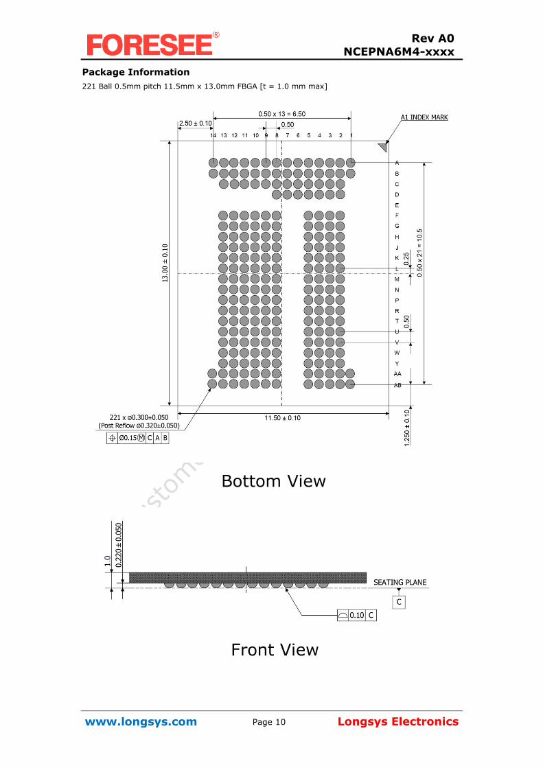
Package Information
221 Ball 0.5mm pitch 11.5mm x 13.0mm FBGA [t = 1.0 mm max]
Bottom View
Front View

Rev A0
NCEPNA6M4-xxxx
www.longsys.com Longsys Electronics Page 11
eMMC Flash

Rev A0
NCEPNA6M4-xxxx
www.longsys.com Longsys Electronics Page 12
1.1 General description
FORESEE eMMC is an embedded storage solution designed in the BGA package. The FORESEE eMMC consists of NAND flash and eMMC controller. The controller could manage the interface protocols, wear-leveling, bad block manage and ECC. FORESEE eMMC has high performance at a competitive cost, high quality and low power consumption, and eMMC is compatible with JEDEC standard eMMC5.0 specification.
Rev A0
NCEPNA6M4-xxxx
www.longsys.com Longsys Electronics Page 13
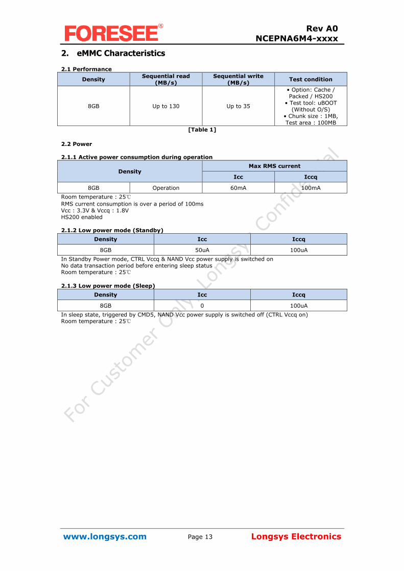
2. eMMC Characteristics 2.1 Performance
Density Sequential read (MB/s)
Sequential write (MB/s) Test condition
8GB Up to 130 Up to 35
• Option: Cache / Packed / HS200
• Test tool: uBOOT (Without O/S)
• Chunk size : 1MB, Test area : 100MB
[Table 1] 2.2 Power
2.1.1 Active power consumption during operation
Density Max RMS current
Icc Iccq
8GB Operation 60mA 100mA
Room temperature : 25℃
RMS current consumption is over a period of 100ms Vcc : 3.3V & Vccq : 1.8V HS200 enabled
2.1.2 Low power mode (Standby) Density Icc Iccq
8GB 50uA 100uA
In Standby Power mode, CTRL Vccq & NAND Vcc power supply is switched on No data transaction period before entering sleep status Room temperature : 25℃
2.1.3 Low power mode (Sleep) Density Icc Iccq
8GB 0 100uA
In sleep state, triggered by CMD5, NAND Vcc power supply is switched off (CTRL Vccq on) Room temperature : 25℃

Rev A0
NCEPNA6M4-xxxx
www.longsys.com Longsys Electronics Page 14
3. eMMC New features for eMMC5.0 3.1 HS200 mode eMMC supports HS200 signaling to achieve a bus speed of 200MB/s via a 200MHz SDR clock frequency. HS200 mode supports only 8-bit bus width and the 1.8V Vccq. Due to the speed, the host may need to have an adjustable sampling point to reliably receive the incoming data (Read Data and CRC Response) with DS pin. eMMC supports up to 5 Driver Strength.
Drive Type
Values Support
Nominal
Impedance
Approximately driving
capability compare to
type_0
Remark
0 Mandatory 50Ω x 1
Default Drive Type。
Supports up to 200MHz
operation。
1
Optional
33Ω x 1.5 Supports up to 200MHz
operation。
2 66Ω x 0.75
The weakest driver that
supports up to 200MHz
operation。
3 100Ω x 0.5
For low noise and low EMI
systems。
Maximal operating
frequency is decided by
host design。
4 40Ω x 1.2
[Table 2]I/O Driver strength types Selecting HS_Timing depends on Host I/F speed, default is 0, but all of value can be selected by host.
Value Timing Supportability for eMMC
0x00 Select backward compatibility interface timing Support
0x01 High speed Support
0x02 HS200 Support
0x03 HS400 Not support
[Table 3]HS_Timing values

Rev A0
NCEPNA6M4-xxxx
www.longsys.com Longsys Electronics Page 15
3.1.1 Bus timing specification in HS200 mode
■ HS200 Device input timing
[Figure 1]HS200 Device input timing
Parameter Symbol Min Max Unit Remark
Output CLK
Cycle time data
transfer mode tPERIOD 5
200MHz(Max),between rising edges
with respect to VT
Slew rate SR 1.125 V/ns With respect to VIH/VIL
Duty cycle
distortion tDSDCD 0.0 0.3 ns
Allowable deviation from the input CLK
duty cycle distortion(tCKDCD)
With respect to VT
Includes jitter,phase noise
Minimum pulse
width tDSMPW 2.2 ns With respect to VT
Output DAT(referenced to data strobe)
Input set-up time tISUddr 0.4 ns CDEVICE≤6pF
With respect to VIH/VIL
Output hold skew tRQH 0.4 0.4 ns CDEVICE≤6pF
With respect to VIH/VIL
Slew rate SR 1.125 V/ns With respect to VIH/VIL
[Table 4]HS200 Device input timing

Rev A0
NCEPNA6M4-xxxx
www.longsys.com Longsys Electronics Page 16
■ HS200 Device output timing Data strobe is for reading data in HS200 mode. Data strobe is toggled only during data read or CRC status response.
[Figure 2]HS200 Device output timing
Parameter Symbol Min Max Unit Remark
Data strobe
Cycle time data
transfer mode tPERIOD 5
200MHz(Max),between rising
edges with respect to VT
Slew rate SR 1.125 V/ns With respect to VIH/VIL and HS200 reference
load
Duty cycle distortion tDSDCD 0.0 0.2 ns
Allowable deviation from the input
CLK duty cycle distortion(tCKDCD)
With respect to VT
Includes jitter,phase noise
Minimum pulse width tDSMPW 2.0 ns With respect to VT
Read pre-amble tRPRE 0.4 5(one clock
cycle) ns
Read post-amble tRPST 0.4 2.5(half
clock cycle) ns
Output DAT(referenced to data strobe)
Input set-up time tISUddr ns CDEVICE≤6pF
With respect to VIH/VIL
Output skew tRQ 0.4 ns With respect to VOH/VOL and HS200
reference load
Output hold skew tRQH 0.4 ns With respect to VOH/VOL and HS200
reference load
Slew rate SR 1.125 V/ns With respect to VOH/VOL and HS200
reference load
[Table 5]HS200 Device output timing

Rev A0
NCEPNA6M4-xxxx
www.longsys.com Longsys Electronics Page 17
Parameter Symbol Min Type Max Unit Remark
Pull-up resistance for CMD
RCMD 4.7 100 Kohm
Pull-up resistance for DAT0-7
RDAT 10 100 Kohm
Pull-down resistance for Data strobe
RDS 10 100 Kohm
Internal pull up resistance DAT1-DAT7
Rint 10 150 Kohm
Bus signal line capacitance
CL 13 pF
Single Device capacitance
CDevice 6 pF
[Table 6]HS200 Capacitance

Rev A0
NCEPNA6M4-xxxx
www.longsys.com Longsys Electronics Page 18
3.2 Field firmware update (FFU)
To download a new firmware, the controller requires instruction sequence following JEDEC standard. Longsys eMMC only supports Manual mode (MODE_OPERATION_CODES is not supported). For more details, refer to the App note.
■ eMMC Field F/W update flow - CMD sequence
Operation CMD Remark
Set block length 512B CMD16, arg : 0x00000200
Enter FFU mode CMD6, arg : 0x031E0100
Send FW to
device(Download) CMD25, arg : 0x00000000
Sending CMD25 is followed by sending FW data ,The whole data should be
sent by one CMD25
CMD12 : Stop CMD12, arg : 0x00000000
CMD6 : Exit FFU mode CMD6, arg : 0x031E0000
HW Reset/Power cycle CMD0 Reset is not support
Re-Init to trans state CMD0, CMD1 ...
Check if FFU is succeeded CMD8, arg : 0x00000000
Check EXT_CSD[26] : FFU_SUCCESS If FFU_SUCCESS is 0, FFU is
succeeded, otherwise FFU is failed. Do not verify data with
CMD17/CMD18 while FFU mode.

Rev A0
NCEPNA6M4-xxxx
www.longsys.com Longsys Electronics Page 19
■ SUPPORTED_MODE[493] (Read Only)
BIT[0] : ‘0’ FFU is not supported by the device.
‘1’ FFU is supported by the device.
BIT[1] : ‘0’ Vendor specific mode (VSM) is not supported by the device.
‘1’ Vendor specific mode is supported by the device.
Bit Field Supportability
Bit[7:2] Reserved -
Bit[1] VSM Not support
Bit[0] FFU Support
■ FFU_FEATURE[492] (Read Only)
BIT[0] : ‘0’ Device does not support MODE_OPERATION_CODES field (Manual mode)
‘1’ Device supports MODE_OPERATION_CODES field (Auto mode)
Bit Field Supportability
Bit[7:1] Reserved -
Bit[0] SUPPORTED_MODE_OPERATION_CODES Not support

Rev A0
NCEPNA6M4-xxxx
www.longsys.com Longsys Electronics Page 20
■ FFU_ARG[490-487] (Read Only)
Using this field the device reports to the host which value the host should set as an argument for read and
write commands in FFU mode.
■ FW_CONFIG[169] (R/W)
BIT[0] : Update disable
0x0 : FW updates enabled.
0x1 : FW update disabled permanently
Bit Field Supportability
Bit[7:1] Reserved -
Bit[0] Update disable FW updates enabled (0x0)
■ FFU_STATUS[26] (R/W/E_P)
Using this field the device reports to the host the state of FFU process
Value Description
0x13 ~ 0xFF Reserved
0x12 Error in downloading Firmware
0x11 Firmware install error
0x10 General error
0x01 ~ 0x0F Reserved
0x00 Success
■ OPERATION_CODES_TIMEOUT[491](Read Only)
Maximum timeout for the SWITCH command when setting a value to the MODE_OPERATION_CODES
field.The register is set to ‘0’, because the controller doesn’t support MODE_OPERATION_CODES.
Value Description Timeout value
0x01 ~ 0x17 MODE_OPERATION_CODES_TIMEOUT = 100us x
2OPERATION_CODES_TIMEOUT (Not defined)
0x18 ~ 0xFF Reserved -
■ MODE_OPERATION_CODES[29] (W/E_P)
The host sets the operation to be performed at the selected mode, in case MODE_CONFIGS is set to
FFU_MODE,MODE_OPERATION_CODES could have the following values :
Value Description
0x01 FFU_INSTALL
0x02 FFU_ABORT
0x00, others Reserved
Rev A0
NCEPNA6M4-xxxx
www.longsys.com Longsys Electronics Page 21
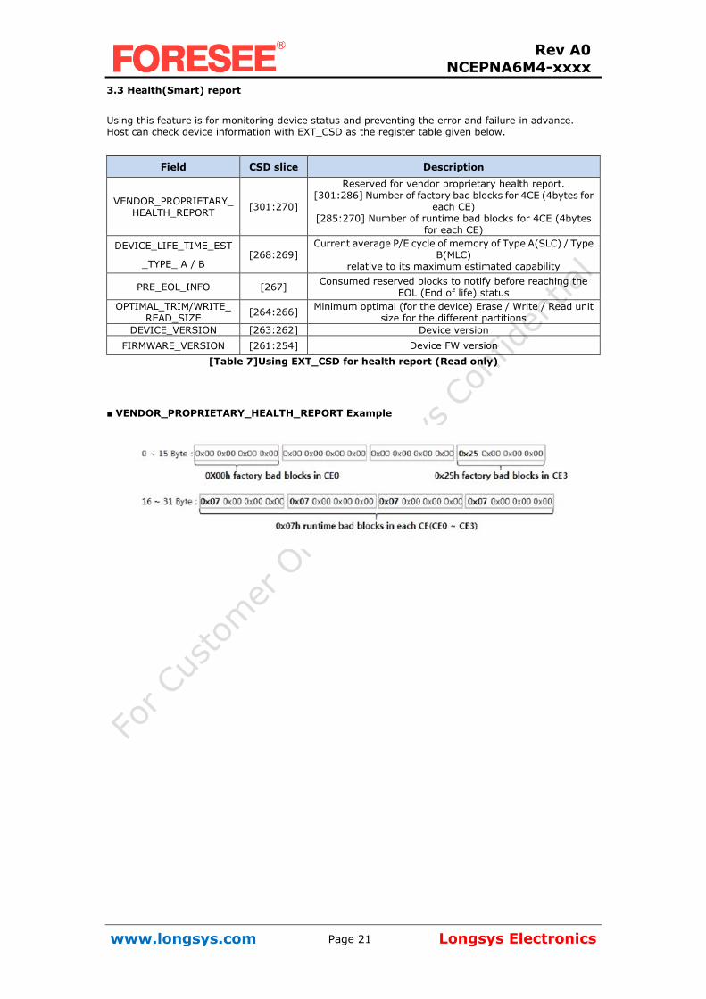
3.3 Health(Smart) report
Using this feature is for monitoring device status and preventing the error and failure in advance. Host can check device information with EXT_CSD as the register table given below.
Field CSD slice Description
VENDOR_PROPRIETARY_HEALTH_REPORT
[301:270]
Reserved for vendor proprietary health report. [301:286] Number of factory bad blocks for 4CE (4bytes for
each CE) [285:270] Number of runtime bad blocks for 4CE (4bytes
for each CE)
DEVICE_LIFE_TIME_EST
_TYPE_ A / B [268:269]
Current average P/E cycle of memory of Type A(SLC) / Type B(MLC)
relative to its maximum estimated capability
PRE_EOL_INFO [267] Consumed reserved blocks to notify before reaching the
EOL (End of life) status
OPTIMAL_TRIM/WRITE_READ_SIZE
[264:266] Minimum optimal (for the device) Erase / Write / Read unit
size for the different partitions
DEVICE_VERSION [263:262] Device version
FIRMWARE_VERSION [261:254] Device FW version
[Table 7]Using EXT_CSD for health report (Read only)
■ VENDOR_PROPRIETARY_HEALTH_REPORT Example
Rev A0
NCEPNA6M4-xxxx
www.longsys.com Longsys Electronics Page 22
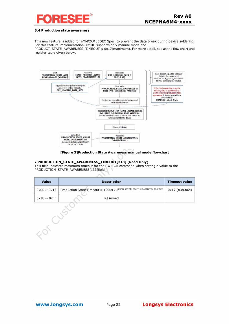
3.4 Production state awareness
This new feature is added for eMMC5.0 JEDEC Spec. to prevent the data break during device soldering. For this feature implementation, eMMC supports only manual mode and PRODUCT_STATE_AWARENESS_TIMEOUT is 0x17(maximum). For more detail, see as the flow chart and register table given below.
[Figure 3]Production State Awareness manual mode flowchart
■ PRODUCTION_STATE_AWARENESS_TIMEOUT[218] (Read Only)
This field indicates maximum timeout for the SWITCH command when setting a value to the PRODUCTION_STATE_AWARENESS[133]field
Value Description Timeout value
0x00 ~ 0x17 Production State Timeout = 100us x 2PRODUCTION_STATE_AWARENESS_TIMEOUT 0x17 (838.86s)
0x18 ~ 0xFF Reserved

Rev A0
NCEPNA6M4-xxxx
www.longsys.com Longsys Electronics Page 23
■ PRODUCTION_STATE_AWARENESS[133](R/W/E) eMMC doesn’t support 0x03 state.
Value Device State Description
0x00 NORMAL (Field) Regular operation
0x01 PRE_SOLDERING_WRITES
0x02 PRE_SOLDERING_POST_WRITES Once transferred to this state the host should not write content to the device
0x03 AUTO_PRE_SOLDERING Not supported
0x04 ~ 0x0F Reserved
0x10 ~ 0x1F Reserved for Vendor Proprietary
Usage
■ PRODUCTION_STATE_AWARENESS_ENABLEMENT[17] eMMC only supports manual mode for PRODUCTION_STATE_AWARENESS
Enablement(R/W/E) Capabilities(R)
Bit7 Bit6 Bit5 Bit4 Bit3 Bit2 Bit1 Bit0
Reserved mode
Production State
Awareness enable
Reserved Auto mode
Supported
Manual mode
Supported
Cleared when PRODUCTION_STATE_AWARENESS is charged to Normal
(either automatically or by setting PRODUCTION_STATE_AWARENESS to Normal)
This bit could be set to
‘1’ only once
Rev A0
NCEPNA6M4-xxxx
www.longsys.com Longsys Electronics Page 24
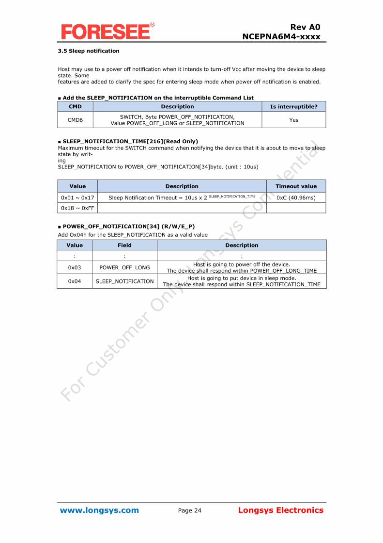
3.5 Sleep notification
Host may use to a power off notification when it intends to turn-off Vcc after moving the device to sleep state. Some features are added to clarify the spec for entering sleep mode when power off notification is enabled.
■ Add the SLEEP_NOTIFICATION on the interruptible Command List
CMD Description Is interruptible?
CMD6 SWITCH, Byte POWER_OFF_NOTIFICATION,
Value POWER_OFF_LONG or SLEEP_NOTIFICATION Yes
■ SLEEP_NOTIFICATION_TIME[216](Read Only)
Maximum timeout for the SWITCH command when notifying the device that it is about to move to sleep state by writ- ing SLEEP_NOTIFICATION to POWER_OFF_NOTIFICATION[34]byte. (unit : 10us)
Value Description Timeout value
0x01 ~ 0x17 Sleep Notification Timeout = 10us x 2 SLEEP_NOTIFICATION_TIME 0xC (40.96ms)
0x18 ~ 0xFF
■ POWER_OFF_NOTIFICATION[34] (R/W/E_P)
Add Ox04h for the SLEEP_NOTIFICATION as a valid value
Value Field Description
: : :
0x03 POWER_OFF_LONG Host is going to power off the device.
The device shall respond within POWER_OFF_LONG_TIME
0x04 SLEEP_NOTIFICATION Host is going to put device in sleep mode.
The device shall respond within SLEEP_NOTIFICATION_TIME

Rev A0
NCEPNA6M4-xxxx
www.longsys.com Longsys Electronics Page 25
3.6 Secure removal type
This feature is used for how information is removed from the physical memory during a purge operation. ■ Secure Removal Type[16]
Among four options for secure removal type, eMMC supports 0x3, 0x1 and 0x0 (0x2 option is not supported) eMMC recommends using a vendor defined removal type(type 3). If host want to erase the device physically using removal type0. Secure erase & Secure trim time is longer than using removal type0
BIT Description of Secure
Removal Type Description Supportability
BIT[5:4] Configure Secure Removal
Type (R/W)
0x3 Information removed using a vendor defined
Support
0x2
Information removed by an overwriting the
addressed locations with a character, its
complement, then a random character
0x1
Information removed by an overwriting the
addressed locations with a
character followed by an erase
0x0
Information removed by an erase of the
physical memory
BIT[3:0] Supported Secure Removal
Type (R)
BIT[3] Information removed using a vendor defined
Support
BIT[2]
Information removed by an overwriting the
addressed locations with a character, its
complement, then a random character
Not support
BIT[1]
Information removed by an overwriting the
addressed locations with a
character followed by an erase
Support
BIT[0]
Information removed by an erase of the
physical memory
Support

Rev A0
NCEPNA6M4-xxxx
www.longsys.com Longsys Electronics Page 26
3.7 RPMB throughput improvement (For future spec in eMMC)
This feature is proposed for RPMB write data size to improve the RPMB throughput at eMMC5.x spec. The
supported maximum data size of RPMB write access is 8KB (32ea). At this moment for eMMC device, supported Max.data size is up to 64ea(16KB). More information is shown as the following tables. ■ RPMB Throughput
FORESEE eMMC provides up to 64ea for RPMB write data size.
Max. data size Using for improve RPMB Throughput
eMMC5.x Spec. 32ea (<=8KB) Setting the EN_RPMB_REL_WR
(Bit[4] of EXT_CSD)[166] ) Value
Foresee eMMC
Available Max. data size is 64ea (<=16KB) REL_WR_SEC_C[222] value is set to ‘10’
(512B chunk based, 8KB) Present setting RPMB write data size is 8KB
■ RPMB Performance with eMMC
Following table shows the RPMB performance with 8KB chunk data on the eMMC device.
RPMB
Performance
512B Data
transfer unit
1KB Data
transfer unit
2KB Data
transfer unit
4KB Data
transfer unit
8KB Data
transfer unit
Sequential Write (Unite : MB/s)
0.6 1 2 3 5
Sequential Read (Unite : MB/s)
4 7 11 15 20

Rev A0
NCEPNA6M4-xxxx
www.longsys.com Longsys Electronics Page 27
3.8 Enhanced features from eMMC4.5 Several eMMC features are changed from eMMC4.5 to enhance the eMMC performance.
Parameter eMMC4.5 eMMC5.0 Description
HPI Features CMD12 CMD13 Following industry wise common
configuration.
Max. Packed CMD size (Read/Write)
8ea 63ea Expended the packed CMD size for
optimized device performance.
Cache size 64KB 128KB Cache size is up to 128KB for optimized
device performance with 4-way interleave implementation.
I/O Driver strength Support Type0 Support all type eMMC supports all of driver strength
types for eMMC5.0
[Table 8]Enhanced features from eMMC4.5

Rev A0
NCEPNA6M4-xxxx
www.longsys.com Longsys Electronics Page 28
4. eMMC general parameters 4.1 Power mode
4.1.1 Leakage
Parameter Symbol Min Max Unit Remark
BGA -0.5 Vccq+0.5 V
All inputs
Input leakage current (before initialization
sequenceand/or the internal- pull up resistors connected)
-100 100 uA
Input leakage current (after initialization sequence
and the internal pull up resistors
disconnected)
-2 2 uA
All outputs
Output leakage current (before initialization sequence)
-100 100 uA
Output leakage current (after initialization sequence)
-2 2 uA
[Table 9]General operation conditions
4.1.2 Power Supply In eMMC, Vcc is used for the NAND core voltage and NAND interface; Vccq is for the controller core and Emmc interface voltage shown in Figure 9. The core regulator is optional and only required when internal core logic voltage is regulated from Vccq. A Creg capacitor must be connected to the VDDi terminal to stabilize regulator output on the system.
[Figure 4]eMMC internal power diagram

Rev A0
NCEPNA6M4-xxxx
www.longsys.com Longsys Electronics Page 29
eMMC supports one or more combinations of V cc and V ccq as shown in Table 15. The available voltage configuration is shown in Table 16.
Parameter Symbol Min Max Unit Remark
Supply voltage (NAND)
Vcc 2.7 3.6 V
1.7 1.95 V Not support
Supply voltage (I/O)
Vccq 2.7 3.6 V
1.7 1.95 V
Supply power-up for
3.3V tPRUH 35 ms
Supply power-up for
1.8V tPRUL 25 ms
[Table 10]eMMC power supply voltage
Vccq
1.7V ~ 1.95V 2.7V ~ 3.6V
Vcc 2.7V–3.6V Valid Valid
1.7V–1.95V Not Valid Not Valid
[Table 11]eMMC voltage combinations

Rev A0
NCEPNA6M4-xxxx
www.longsys.com Longsys Electronics Page 30
4.2 Connection Guide
Parameter Symbol Min Max Recommend Unit Remark
Pull-up resistance for CMD
R_CMD 4.7 100 10 kohm Pull-up resistance should be put on
CMD line to prevent bus floating.
Pull-up resistance for DAT0~7
R_DAT 10 199 50 kohm Pull-up resistance should be put on DAT line to prevent bus floating.
Data strobe(DS) R_DS NC NC NC
It is not necessary to put pull-up/pull-down resistance on
DS line since DS is internally pulled down. Direct connection to host is required and please float this pin if
it is not used
Pull-up resistance for RSTn
R_RSTn 10 100 50 kohm
It is not necessary to put pull-up resistance on RSTn line if host
does not use H/W reset. (Extended CSD register [162] =
0b)
Serial resistance on CLK
R_CLK 0 30 27 ohm
To reduce overshooting/undershooting
Note: If the host uses HS200, we recommend to remove this
resister for better CLK signal
Vccq capacitor value
C1 & C2 2±0.22 4.7 2.2±0.22 uF Coupling cap should be connected with Vccq and Vssqm as closely
possible.
Vcc capacitor value(≤8GB)
C3 & C4 4.72±10% 10 4.7±10% uF
Coupling cap should be connected with Vcc and Vssm as closely
possible. Vcc /Vccq cap. value would be up
to Host requirement and the application
system characteristics.
VCC capacitor value(>8GB)
VDDi capacitor value
C5 & C6 0 2.2 0.1 uF
Coupling cap should be connected with VDDi and Vssq as closely
possible. (Internal Cap : 1uF)
[Table 12]Connection guide specification

Rev A0
NCEPNA6M4-xxxx
www.longsys.com Longsys Electronics Page 31
5. eMMC basic operations
5. Partitioning
5.1 User density
[Figure 5]Partition diagram ■ Boot partition size
Density Boot Partition 1,2
8GB 4096KB

Rev A0
NCEPNA6M4-xxxx
www.longsys.com Longsys Electronics Page 32
5.2 Erase / Write protect group size
Density Erase group size Write protect group
size ERASE_GROUP_DER=0 ERASE_GROUP_DER=1
8GB 512KB 512KB 8MB
[Table 13]Erase / Write protect Group size

Rev A0
NCEPNA6M4-xxxx
www.longsys.com Longsys Electronics Page 33
6. Time out
Timing parameter Value Remark
Read timeout 100ms
Write timeout(CMD to write Done)
Max 500ms
Erase timeout Max 600ms Erase group size : 512KB
Force erase timeout Max 3min
Discard timeout Max 600ms
Trim timeout Max 600ms
Secure trim Max 6s Unmapping only
Sanitize 8GB:8min
Foresee recommends to erase all blocks before
sanitize operation to shorten the sanitize time
Secure erase Max 6s Unmapping only
Initialization timeout Max 1s CMD to Response
1st Initialization timeout after partitioning
Max 1s BOOT1/2, RPMB, UDA & EUDA
PON busy Time (Short / Long) Max 50ms/1000ms PON long busy time includes
garbage collection time.
Initialization after PON (Short / Long)
Max 180ms
BKOP exit Time Max 100ms BKOP off time after HPI
Auto-BKOP exit Time Max 100ms BKOP off time after any CMD
from host
HPI Max 100ms Response after HPI
CMD5 sleep In 3ms
[Table 14]Time out value eMMC I/F : HS200 Pre-conditioning states - Clean state / Test Range : Random write - 1GB, Random read - 1GB Sequential read / write chunk size : 1MB Current numbers are based on aligned 4KB Maximum 4-way interleaving

Rev A0
NCEPNA6M4-xxxx
www.longsys.com Longsys Electronics Page 34
7. Device registers
There are six different registers within the device interface: •Operation conditions register (OCR) •Card identification register (CID) •Card specific data register (CSD) •Relative card address register (RCA) •DSR (Driver Stage Register) •Extended card specific data register (EXT_CSD). These registers are used for the serial data communication and can be accessed only using the corresponding commands. eMMC has a status register to provide information about the current device state and completion codes for the last host command. 7.1 Operation conditions register (OCR) The 32-bit operation conditions register (OCR) stores the VDD voltage profile of eMMC and the access mode indication. In addition, this register includes a status information bit. This status bit is set if eMMC power up procedure has been finished.
OCR bit Description Foresee eMMC
[6:0] Reserved 000 0000b
[7] 1.70V – 1.95V 1b
[14:8] 2.0 – 2.6 000 0000b
[23:15] 2.7 - 3.6 (High Vccq range) 1111 1111 1b
[28:24] Reserved 000 000b
[30:29] Access mode 10b(sector mode)
[31] (card power up status bit (busy))(1)
[Table 15]OCR register definition 1) This bit is set to LOW if the card has not finished the power up routine

Rev A0
NCEPNA6M4-xxxx
www.longsys.com Longsys Electronics Page 35
7.2 Card identification (CID) register The card identification (CID) register is 128 bits wide. It contains eMMC identification information used during eMMC identification phase (eMMC protocol). Every individual eMMC has a unique identification number. The structure of the CID register is defined in the following sections.
Name Field Width CID slice CID value Remark
Manufacturer ID MID 8 [127:120] 88h
Reserved 6 [119:114]
Card/BGA CBX 2 [113:112] 01h BGA
OEM/application ID OID 8 [111:104] 03h
Product name PNM 48 [103:56] 0x4E4361726420
Product revision PRV 8 [55:48] 02h
Product serial number
PSN 32 [47:16] Not Fixed
Manufacturing date MDT 8 [15:8] Not Fixed
CRC7 checksum CRC 7 [7:1] Not Fixed
Not used, always '1' Reserved 1 [0:0] 1
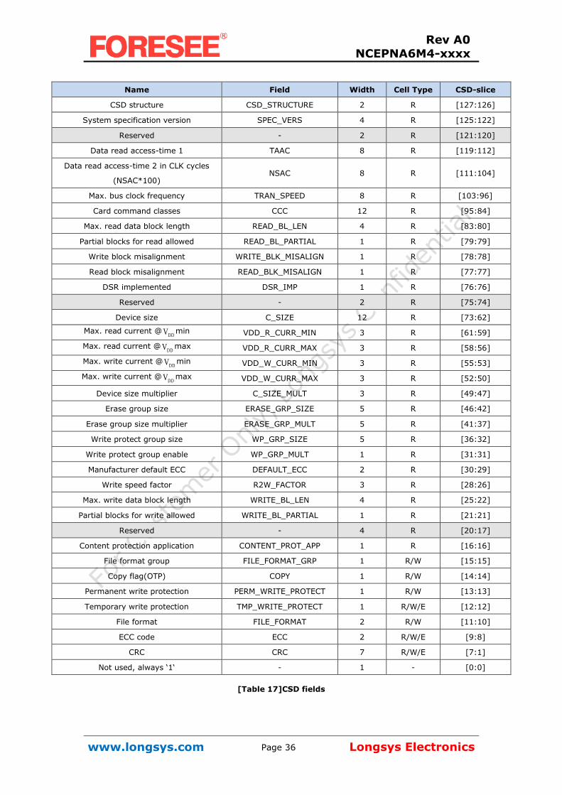
[Table 16]Card identification (CID) fields 7.3 Card specific data register (CSD) The card specific data (CSD) register provides information on how to access eMMC contents. The CSD defines the data format, error correction type, maximum data access time, data transfer speed and so on. The programmable part of the register (entries marked by W or E, see below) can be changed by CMD27. The type of the CSD Registry entries in the Table 20 below is coded as follows: • R: Read only.
• W: One time programmable and not readable.
• R/W: One time programmable and readable.
• W/E: Multiple writable with value kept after power failure, H/W reset assertion and any CMD0 reset and not readable.
• R/W/E: Multiple writable with value kept after power failure, H/W reset assertion and any CMD0 reset and readable.
• R/W/C_P: Writable after value cleared by power failure and HW/rest assertion (the value not cleared by CMD0 reset)
and
readable. • R/W/E_P: Multiple writable with value reset after power failure, H/W reset assertion and any CMD0 reset and readable.
• W/E_P: Multiple writable with value reset after power failure, H/W reset assertion and any CMD0 reset and not
readable.
Rev A0
NCEPNA6M4-xxxx
www.longsys.com Longsys Electronics Page 36
Name Field Width Cell Type CSD-slice
CSD structure CSD_STRUCTURE 2 R [127:126]
System specification version SPEC_VERS 4 R [125:122]
Reserved - 2 R [121:120]
Data read access-time 1 TAAC 8 R [119:112]
Data read access-time 2 in CLK cycles
(NSAC*100) NSAC 8 R [111:104]
Max. bus clock frequency TRAN_SPEED 8 R [103:96]
Card command classes CCC 12 R [95:84]
Max. read data block length READ_BL_LEN 4 R [83:80]
Partial blocks for read allowed READ_BL_PARTIAL 1 R [79:79]
Write block misalignment WRITE_BLK_MISALIGN 1 R [78:78]
Read block misalignment READ_BLK_MISALIGN 1 R [77:77]
DSR implemented DSR_IMP 1 R [76:76]
Reserved - 2 R [75:74]
Device size C_SIZE 12 R [73:62]
Max. read current @DDV min VDD_R_CURR_MIN 3 R [61:59]
Max. read current @DDV max VDD_R_CURR_MAX 3 R [58:56]
Max. write current @DDV min VDD_W_CURR_MIN 3 R [55:53]
Max. write current @DDV max VDD_W_CURR_MAX 3 R [52:50]
Device size multiplier C_SIZE_MULT 3 R [49:47]
Erase group size ERASE_GRP_SIZE 5 R [46:42]
Erase group size multiplier ERASE_GRP_MULT 5 R [41:37]
Write protect group size WP_GRP_SIZE 5 R [36:32]
Write protect group enable WP_GRP_MULT 1 R [31:31]
Manufacturer default ECC DEFAULT_ECC 2 R [30:29]
Write speed factor R2W_FACTOR 3 R [28:26]
Max. write data block length WRITE_BL_LEN 4 R [25:22]
Partial blocks for write allowed WRITE_BL_PARTIAL 1 R [21:21]
Reserved - 4 R [20:17]
Content protection application CONTENT_PROT_APP 1 R [16:16]
File format group FILE_FORMAT_GRP 1 R/W [15:15]
Copy flag(OTP) COPY 1 R/W [14:14]
Permanent write protection PERM_WRITE_PROTECT 1 R/W [13:13]
Temporary write protection TMP_WRITE_PROTECT 1 R/W/E [12:12]
File format FILE_FORMAT 2 R/W [11:10]
ECC code ECC 2 R/W/E [9:8]
CRC CRC 7 R/W/E [7:1]
Not used, always ‘1‘ - 1 - [0:0]
[Table 17]CSD fields

Rev A0
NCEPNA6M4-xxxx
www.longsys.com Longsys Electronics Page 37
7.4 Extended CSD register
The Extended CSD register defines eMMC properties and selected modes. It is 512 bytes long. The most significant 320 bytes are the Properties segment, which defines eMMC capabilities and cannot be modified by the host. The lower 192 bytes are the modes segment, which defines the configuration eMMC is wo rking in. These modes can be changed by the host by means of the switch command.
Name Field Size Type Slice
[bytes] Value Description
Reserved 7 [511:505] 0h
Supported Command
Sets S_CMD_SET 1 R [504] 1h
HPI Features HPI_FEATURES 1 R [503] 1h HPI type
CMD12
Background
operations support BKOPS_SUPPORT 1 R [502] 1h
BKOPS
supported
Max packed read
command MAX_PACKED_READS 1 R [501] 3Fh
Max packed write
command MAX_PACKED_WRITES 1 R [500] 3Fh
Data Tag Support DATA_TAD_SUPPORT 1 R [499] 1h
Tag Unit Size TAG_UNIT_SIZE 1 R [498] 4h
Tag Resource Size TAG_RES_SIZE 1 R [497] 0h
Context management
capabilities CONTEXT_CAPABITILITIES 1 R [496] 5h
Large Unit size LARGE_UNIT_SIZE_M1 1 R [495] 7h
Large Unit
size
8MB
Extended partitions
attribute support EXT_SUPPORT 1 R [494] 3h
Supported modes SUPPORTED_MODES 1 R [493] 3h
Reserved 191 [492:302] 0h
Vendor proprietary
health report
VENDOR_PROPRIETARY_HEA
LTH_REPORT 1 R
[301:27
0] 0h
Device life time
estimation type B
DEVICE_LIFE_TIME_EST_TYP
_B 1 R [269] 1h
Device life time
estimation type A
DEVICE_LIFE_TIME_EST_TYP
_A 1 R [268] 1h
Pre EOL information PRE_EOL_INFO 1 R [267] 1h
Optimal read size OPTIMAL_READ_SIZE 1 R [266] 0h
Optimal write size OPTIMAL_WRITE _SIZE 1 R [265] 4h
Optimal trim unit size OPTIMAL_TRIM_UNIT_SIZE 1 R [264] 1h

Rev A0
NCEPNA6M4-xxxx
www.longsys.com Longsys Electronics Page 38
Name Field Size Type Slice
[bytes] Value Description
Reserved
11 [263:253] TBD
Cache size CACHE_SIZE 4 R [252:24
9] 10000h
Generic CMD6 timeout GENERIC_CMD6_TIME 1 R [248] Ah
Generic
CMD6
timeout
100ms
Power-off
notification(long)
timeout
POWER_OFF_LONG_TIME 1 R [247] 3Ch
Power off
notification(l
ong) timeout
600ms
Background
operations status BKOPS_STATUS 1 R [246] 0h
No
operations
required
Number of correctly
programmed sectors
CORRECTLY_PRG_SECTORS_
NUM 4 R [245:242] 0h
First Initialization time
after partitioning INI_TIMEOUT_AP 1 R [241] 1Eh
initial time
out 3s
Reserved
1 [240] 0h
Power class for
52Mhz,DDR at 3.6V PWR_CL_DDR_52_360 1 R [239] 0h
rms 100 mA,
peak 200 mA
Power class for
52Mhz,DDR at 1.95V PWR_CL_DDR_52_195 1 R [238] 0h
rms 65 mA,
peak 130 mA
Reserved
2 [237:236] 0h
Minimum write
performance for 8bit
at 52MHz in DDR
mode
MIN_PERF_DDR_W_8_52 1 R [235] 0h
For cards not
reaching the
4.8 MB/s
value
Only support
SDR
Minimum read
performance for 8bit
at 52MHz in DDR
mode
MIN_PERF_DDR_R_8_52 1 R [234] 0h
For cards not
reaching the
4.8MB/s
value
Reserved
1 [233] 0h
TRIM Multiplier TRIM_MULT 1 R [232] 5h trim time out
1.5s

Rev A0
NCEPNA6M4-xxxx
www.longsys.com Longsys Electronics Page 39
Name Field Size Type Slice
[bytes] Value Description
Secure feature
support SEC_FEATURE_SUPPORT 1 R [231] 55h
1. Support
the secure
and insecure
trim
operations.
2. Support
the
automatic
secure purge
operation on
retired
defective
portions of
the array.
3. Secure
purge
operations
are
supported.
4.Support
the sanitize
operation
Secure Erase
Multiplier SEC_ERASE_MULT 1 R [230] 1Bh
secure erase
time out 81s
Secure TRIM Multiplier SEC_TRIM_MULT 1 R [229] 11h
secure trim
time out
51s
Boot Information BOOT_INFO 1 R [228] 7h
1. Support
high
speed
timing
boot.
2. Support
dual
data rate
during
boot
3. Support
alternati
ve boot
method
Reserved
1 [227] 0h
Rev A0
NCEPNA6M4-xxxx
www.longsys.com Longsys Electronics Page 40
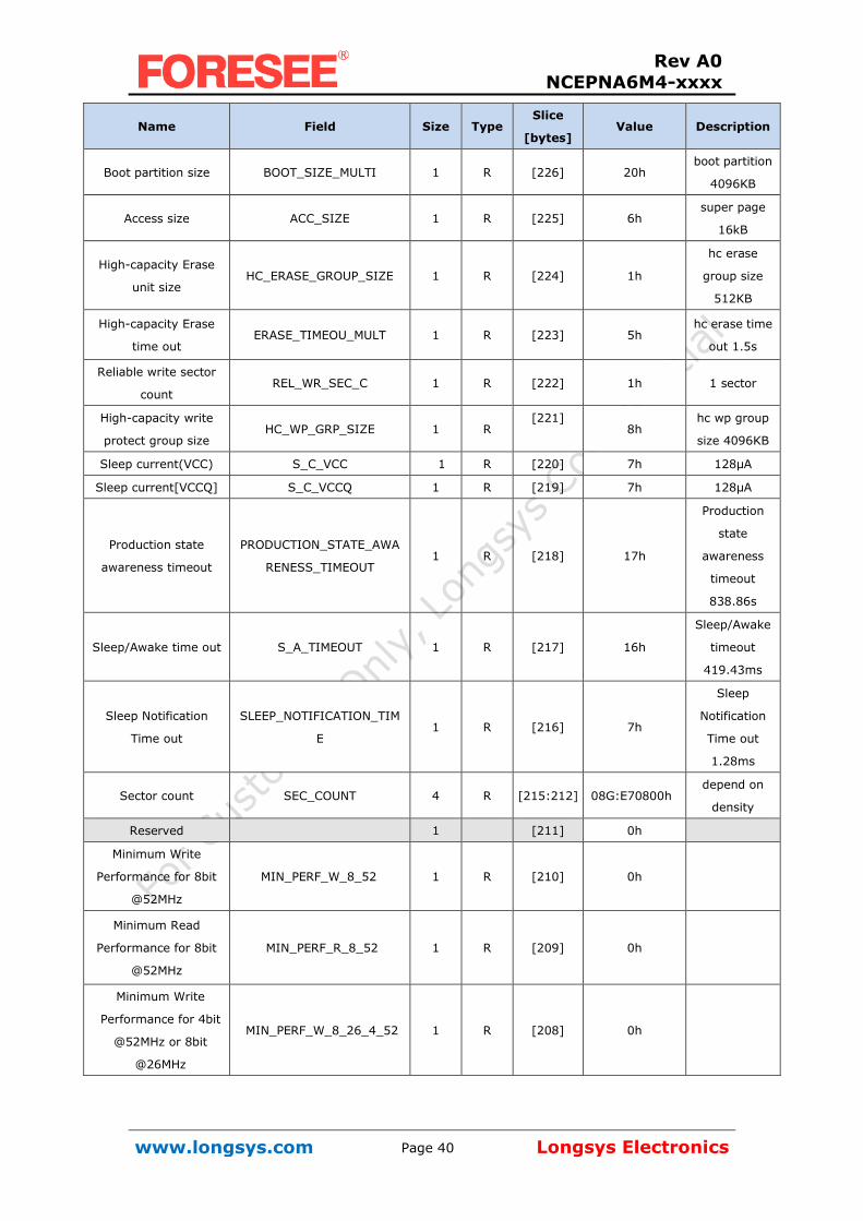
Name Field Size Type Slice
[bytes] Value Description
Boot partition size BOOT_SIZE_MULTI 1 R [226] 20h boot partition
4096KB
Access size ACC_SIZE 1 R [225] 6h super page
16kB
High-capacity Erase
unit size HC_ERASE_GROUP_SIZE 1 R [224] 1h
hc erase
group size
512KB
High-capacity Erase
time out ERASE_TIMEOU_MULT 1 R [223] 5h
hc erase time
out 1.5s
Reliable write sector
count REL_WR_SEC_C 1 R [222] 1h 1 sector
High-capacity write
protect group size HC_WP_GRP_SIZE 1 R
[221]
8h
hc wp group
size 4096KB
Sleep current(VCC) S_C_VCC 1 R [220] 7h 128μA
Sleep current[VCCQ] S_C_VCCQ 1 R [219] 7h 128μA
Production state
awareness timeout
PRODUCTION_STATE_AWA
RENESS_TIMEOUT 1 R [218] 17h
Production
state
awareness
timeout
838.86s
Sleep/Awake time out S_A_TIMEOUT 1 R [217] 16h
Sleep/Awake
timeout
419.43ms
Sleep Notification
Time out
SLEEP_NOTIFICATION_TIM
E 1 R [216] 7h
Sleep
Notification
Time out
1.28ms
Sector count SEC_COUNT 4 R [215:212] 08G:E70800h depend on
density
Reserved
1 [211] 0h
Minimum Write
Performance for 8bit
@52MHz
MIN_PERF_W_8_52 1 R [210] 0h
Minimum Read
Performance for 8bit
@52MHz
MIN_PERF_R_8_52 1 R [209] 0h
Minimum Write
Performance for 4bit
@52MHz or 8bit
@26MHz
MIN_PERF_W_8_26_4_52 1 R [208] 0h

Rev A0
NCEPNA6M4-xxxx
www.longsys.com Longsys Electronics Page 41
Name Field Size Type Slice
[bytes] Value Description
Minimum Read
Performance for 4bit
@52MHz or 8bit
@26MHz
MIN_PERF_R_8_26_4_52 1 R [207] 0h
Minimum Write
Performance for 4bit
@26MHz
MIN_PERF_W_4_26 1 R [206] 0h
Minimum Read
Performance for 4bit
@26MHz
MIN_PERF_R_4_26 1 R [205] 0h
Reserved
1 [204] 0h
Power Class for 26MHz
@3.6V PWR_CL_26_360 1 R [203] 0h
rms 100 mA,
peak 200 mA
Power Class for 52MHz
@3.6V PWR_CL_52_360 1 R [202] 0h
rms 100 mA,
peak 200 mA
Power Class for 26MHz
@1.95V PWR_CL_26_195 1 R [201] 0h
rms 65 mA,
peak 130 mA
Power Class for 52MHz
@1.95V PWR_CL_52_195 1 R [200] 0h
rms 65 mA,
peak 130 mA
Partition switching
timing PARTITION_SWITCH_TIME 1 R [199] 1h
Partition
switch time
out 10ms
Out-of-interrupt busy
timing OUT_OF_INTERRUPT_TIME 1 R [198] 5h
HPI time out
50ms
I/O Driver Strength DRIVER_STRENGTH 1 R [197] 1h
Card Type CARD_TYPE 1 R [196] 17h
HS200 SDR
eMMC@200M
hz-1.8V I/0
Reserved
1 [195] 0h
CSD Structure Version CSD_STRUCTURE 1 R [194] 2h CSD version
No. 1.2
Reserved
1 [193] 0h
Extended CSD
Revision EXT_CSD_REV 1 R [192] 7h
Revision 1.7
(for MMC
v5.0,v5.01)
Command Set CMD_SET 1 R/W/
E_P [191] 0h
Reserved
1 [190] 0h
Command set revision CMD_SET_REV 1 R [189] 0h v4.0
Reserved
1 [188] 0h

Rev A0
NCEPNA6M4-xxxx
www.longsys.com Longsys Electronics Page 42
Name Field Size Type Slice
[bytes] Value Description
Power class POWER_CLASS 1 R/W/
E_P [187] 0h
Reserved
1 [186] 0h
High Speed Interface
Timing HS_TIMING 1
R/W/
E_P [185] 1h High Speed
Reserved
1 [184] 0h
Bus Width Mode BUS_WIDTH 1 W/E_
P [183] 0h
Reserved
1 [182] 0h
Erased memory range ERASE_MEM_CONT 1 [181] 0h
Reserved
1 [180] 0h
Partition Configuration PARTITION_CONFIG 1
R/W/
E
R/W/
E_P
[179] 0h
Boot config protection BOOT_CONFIG_PROT 1
R/W
R/W/
C_P
[178] 0h
Boot bus width1 BOOT_BUS_WIDTH 1 R/W/
E [177] 0h
Reserved
1 [176] 0h
High-density erase
group definition ERASE_GROUP_DEF 1
R/W/
E_P [175] 0h
Reserved
1 [174] 0h
Boot area write
protect register BOOT_WP 1
R/W
R/W/
C_P
[173] 0h
Reserved
1 [172] 0h
User area write
protect register USER_WP 1
R/W
R/W/
C_P
R/W/
E_P
[171] 0h
Reserved
1 [170] 0h
FW Configuration FW_CONFIG 1 R/W [169] 0h
RPMB Size RPMB_SIZE_MULT 1 R [168] 20h RPMB size
is 4MB
Write reliability
setting register WR_REL_SET 1 R/W [167] 0h

Rev A0
NCEPNA6M4-xxxx
www.longsys.com Longsys Electronics Page 43
Name Field Size Type Slice
[bytes] Value Description
Write reliability
parameter register WR_REL_PARAM 1 R [166] 5h
Support the
enhanced
definition of
reliable write
Reserved
1 [165] 0h
Manually start
background
operations
BKOPS_START 1 W/E_
P [164] 0h
Enable background
operations handshake BKOPS_EN 1 R/W [163] 0h
H/W reset function RST_n_FUNCTION 1 R/W [162] 0h
Reserved
1 [161] 0h
Partitioning support PARTITIONING_SUPPORT 1 R [160] 7h
1. Enhanced
technological
features in
partitions
and user data
area.
2. Device
supports
partitioning
features
3. Device can
have
extended
partition
attribute
Max Enhanced Area
Size MAX_ENH_SIZE_MULT 3 R
[159:15
7] 100h
Partitions attribute PARTITIONS_ATTRIBUTE 1 R/W [156] 0h
General Purpose
Partition Size GP_SIZE_MULT 12 R/W
[154:14
3] 0h
Enhanced User Data
Area Size ENH_SIZE_MULT 3 R/W
[142:14
0] 0h
Enhanced User Data
Start Address ENH_START_ADDR 4 R/W
[139:13
6] 0h
Reserved
1 [135] 0h
Secure Bad Block
Management Mode SEC_BAD_BLK_MGMNT 1 R/W [134] 0h
Rev A0
NCEPNA6M4-xxxx
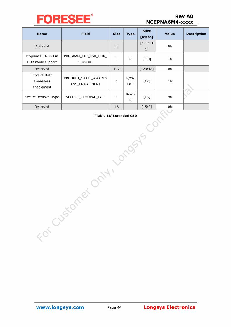
www.longsys.com Longsys Electronics Page 44
Name Field Size Type Slice
[bytes] Value Description
Reserved
3 [133:13
1] 0h
Program CID/CSD in
DDR mode support
PROGRAM_CID_CSD_DDR_
SUPPORT 1 R [130] 1h
Reserved
112 [129:18] 0h
Product state
awareness
enablement
PRODUCT_STATE_AWAREN
ESS_ENABLEMENT 1
R/W/
E&R [17] 1h
Secure Removal Type SECURE_REMOVAL_TYPE 1 R/W&
R [16] 9h
Reserved
16 [15:0] 0h
[Table 18]Extended CSD

Rev A0
NCEPNA6M4-xxxx
www.longsys.com Longsys Electronics Page 45
LPDDR3
SDRAM

Rev A0
NCEPNA6M4-xxxx
www.longsys.com Longsys Electronics Page 46
Functional Description LPDDR3-SDRAM is a high-speed synchronous DRAM device internally configured as an 8-bank memory. These devices contain the following number of bits: 4 Gb has 4,294,967,296 bits 8 Gb has 8,589,934,592 bits 16 Gb has 17,179,869,184 bits 32 Gb has 34,359,738,368 bits LPDDR3 devices use a double data rate architecture on the Command/Address (CA) bus to reduce the number of input pins in the system. The 10-bit CA bus contains command, address, and bank information. Each command uses one clock cycle, during which command information is transferred on both the positive and negative edge of the clock. These devices also use a double data rate architecture on the DQ pins to achieve high speed operation.
The double data rate architecture is essentially an 8n prefetch architecture with an interface designed to transfer two data bits per DQ every clock cycle at the I/O pins. A single read or write access for the LPDDR3 SDRAM effectively consists of a single 8n-bit wide, one clock cycle data transfer at the internal DRAM core and eight corresponding n-bit wide, one-half-clock-cycle data transfers at the I/O pins. Read and write accesses to the LPDDR3 SDRAMs are burst oriented; accesses start at a selected location and continue for a programmed number of locations in a programmed sequence. Accesses begin with the registration of an Activate command, which is then followed by a Read or Write command. The address and BA bits registered coincident with the Activate command are used to select the row and the bank to be accessed. The address bits registered coincident with the Read or Write command are used to select the bank and the starting column location for the burst access. Prior to normal operation, the LPDDR3 SDRAM must be initialized. The following section provides detailed information covering device initialization, register definition, command description and device operation.
LPDDR3 SDRAM Addressing
Density 4Gb 8Gb 16Gb
Number of Banks 8 8 8
Banks Addresses BA0 – BA2 BA0 – BA2 BA0 – BA2
tREFI(us) 3.9 3.9 3.9
X16 Row Addresses R0 – R13 R0 – R14 R0 – R14
Column Addresses C0 – C10 C0 – C10 C0 – C11
X32 Row Addresses R0 – R13 R0 – R14 R0 – R14
Column Addresses C0 – C9 C0 – C9 C0 – C10
Note: 1. The least-significant column address C0, C1 is not transmitted on the CA bus, and is implied to be zero. 2. tREFI values for all bank refresh is Tc = -30 ~ 85 °C, Tc means Operating Case Temperature. 3. Row and Column Address values on the CA bus which are not used are “don’t care”.

Rev A0
NCEPNA6M4-xxxx
www.longsys.com Longsys Electronics Page 47
STATE DIAGRAM
PR(A) = Precharge (All)
ACT = Activate WR(A) = Write (with Autoprecharge) RD(A) = Read (with Autoprecharge)
RESET = Reset is achieved through MRW command MRW = Mode Register Write MRR = Mode Register Read
PD = Enter Power Down PDX = Exit Power Down SREF = Enter Self Refresh SREFX = Exit Self Refresh DPD = Enter Deep Power Down DPDX = Exit Deep Power Down
REF = Refresh

Rev A0
NCEPNA6M4-xxxx
www.longsys.com Longsys Electronics Page 48
Note:
1. In the Idle state, all banks are precharged.
2. In the case of MRW to enter CA Training mode or Write Leveling Mode, the state machine will not automatically return
to the Idle
state. In these cases an additional MRW command is required to exit either operating mode and return to the Idle state. See sections
"CA Training" or "Write Leveling".
3. Terminated bursts are not allowed. For these state transitions, the burst operation must be completed before the
transition can occur.
4. Use caution with this diagram. It is intended to provide a floorplan of the possible state transitions and commands to
control them,
not all details. In particular, situations involving more than one bank are not captured in full detail.

Rev A0
NCEPNA6M4-xxxx
www.longsys.com Longsys Electronics Page 49
Power-up, Initialization and Power-off
Voltage Ramp and Device Initialization The following sequence must be used to power up the device. Unless specified otherwise, this procedure is mandatory. 1. Voltage Ramp While applying power (after Ta), CKE must be held LOW (≤ 0.2 × VDDCA), and all other inputs must be between VILmin and VIHmax. The device outputs remain at High-Z while CKE is held LOW. Following the completion of the voltage ramp (Tb), CKE must be maintained LOW. DQ, DM, DQS_t and DQS_c voltage levels must be between VSSQ and VDDQ during voltage ramp to avoid latchup. CK_t, CK_c, CS_n, and CA input levels must be between VSSCA and VDDCA during voltage ramp to avoid latch-up. Voltage ramp power supply requirements are provided in the table “Voltage Ramp Conditions”.
Table. Voltage Ramp Conditions
After… Applicable Conditions
Ta is reached
VDD1 must be greater than VDD2-200mV.
VDD1 and VDD2 must be greater than VDDCA-200mV.
VDD1 and VDD2 must be greater than VDDQ-200mV.
VREF must always be less than all other supply voltages.
Note:
1. Ta is the point when any power supply first reaches 300mV.
2. Noted conditions apply between Ta and power-off (controlled or uncontrolled).
3. Tb is the point at which all supply and reference voltages are within their defined operating ranges.
4. Power ramp duration tINIT0 (Tb - Ta) must not exceed 20ms.
5. The voltage difference between any of VSS, VSSQ, and VSSCA pins must not exceed 100mV.
Beginning at Tb, CKE must remain LOW for at least tINIT1, after which CKE can be asserted HIGH. The clock must be stable at least tINIT2 prior to the first CKE LOW-to-HIGH transition (Tc). CKE, CS_n, and
CA inputs must observe setup and hold requirements (tIS, tIH) with respect to the first rising clock edge (as well as to subsequent falling and rising edges). If any MRR commands are issued, the clock period must be within the range defined for tCKb. MRW commands can be issued at normal clock frequencies as long as all AC timings are met. Some AC parameters (for example, tDQSCK) could have relaxed timings (such as tDQSCKb) before the system is appropriately configured. While keeping CKE HIGH, NOP commands must be issued for at least tINIT3 (Td). The ODT input signal may be in undefined state until tIS before CKE is registered HIGH. When CKE is registered HIGH, the ODT input signal shall be statically held at either LOW or HIGH. The ODT input signal remains static until the power up initialization sequence is finished, including the expiration of tZQINIT. 2. Reset Command
After tINIT3 is satisfied, the MRW RESET command must be issued (Td). An optional PRECHARGE ALL command can be issued prior to the MRW RESET command. Wait at least tINIT4 while keeping CKE asserted and issuing NOP commands. Only NOP commands are allowed during time tINIT4.

Rev A0
NCEPNA6M4-xxxx
www.longsys.com Longsys Electronics Page 50
3. MRRs and Device Auto Initialization (DAI) Polling After tINIT4 is satisfied (Te), only MRR commands and power-down entry/exit commands are supported. After Te, CKE can go LOW in alignment with power-down entry and exit specifications. MRR commands are only valid at this time if the CA bus does not need to be trained. CA Training may only begin after time Tf. Use the MRR command to poll the DAI bit and report when device auto initialization is complete; otherwise, the controller must wait a minimum of tINIT5, or until the DAI bit is set before proceeding. As the memory output buffers are not properly configured by Te, some AC parameters must have relaxed timings before the system is appropriately configured. After the DAI bit (MR0, DAI) is set to zero by the memory device (DAI complete), the device is in the idle state (Tf).DAI status can be determined by issuing the MRR command to MR0. The device sets the DAI bit no later than tINIT5 after the RESET command. The controller must wait at least tINIT5 or until the DAI bit is set before proceeding. 4. ZQ Calibration If CA Training is not required, the MRW initialization calibration (ZQ_CAL) command can be issued to the memory (MR10) after time Tf. If CA Training is required, the CA Training may begin at time Tf. See the section of "Mode Register Write - CA Training Mode" for the CA Training command. No other CA commands (other than RESET or NOP) may be issued prior to the completion of CA Training. At the completion of CA Training (Tf'), the MRW initialization calibration (ZQ_CAL) command can be issued to the memory (MR10). This command is used to calibrate output impedance over process, voltage, and temperature. In systems where more than one LPDDR3 device exists on the same bus, the controller must not overlap MRW ZQ_CAL commands. The device is ready for normal operation after tZQINIT. 5. Normal Operation After tZQINIT (Tg), MRW commands must be used to properly configure the memory (for example the output buffer drive strength, latencies, etc.). Specifically, MR1, MR2, and MR3 must be set to configure the memory for the target frequency and memory configuration. After the initialization sequence is complete, the device is ready for any valid command. After Tg, the clock frequency can be changed using the procedure described in the LPDDR3 specification.
Table. Timing Parameters for initialization
Symbol Parameter Value
Unit min max
tINIT0 Maximum Voltage Ramp Time 20 Ms
tINIT1 Minimum CKE low time after completion of
voltage ramp 100 Ns
tINIT2 Minimum stable clock before first CKE high 5 tCK
tINIT3 Minimum idle time after first CKE assertion 200 us
tINIT4 Minimum idle time after Reset command 1 us
tINIT5 Maximum duration of Device
Auto-Initialization 10 us
tZQINIT ZQ Initial Calibration for LPDDR3 devices 1 us
tCKb Clock cycle time during boot 18 100 us

Rev A0
NCEPNA6M4-xxxx
www.longsys.com Longsys Electronics Page 51
Figure. Power Ramp and Initialization Sequence
Notes 1. High-Z on the CA bus indicates NOP. 2. For tINIT values, see the table "Timing Parameters for Initialization". 3. After RESET command (time Te), RTT is disabled until ODT function is enabled by MRW to MR11 following Tg. 4. CA Training is optional. Initialization After Reset (without Power ramp) If the RESET command is issued before or after the power-up initialization sequence, the re-initialization
procedure must begin at Td.

Rev A0
NCEPNA6M4-xxxx
www.longsys.com Longsys Electronics Page 52
Power-off Sequence The following procedure is required to power off the device. While powering off, CKE must be held LOW (≤ 0.2 × VDDCA); all other inputs must be between VILmin and VIHmax.The device outputs remain at High-Z while CKE is held LOW. DQ, DM, DQS_t, and DQS_c voltage levels must be between VSSQ and VDDQ during the power-off sequence to avoid latch-up. CK_t, CK_c, CS_n, and CA input levels must be between VSSCA and VDDCA during the power-off sequence to avoid latch-up. Tx is the point where any power supply drops below the minimum value specified. Tz is the point where all power supplies are below 300mV. After Tz, the device is powered off (see the table “Power Supply Conditions”).
Table. Power Supply Conditions
Between… Applicable Conditions
Tx and Tz
VDD1 must be greater than VDD2—200mV
VDD1 must be greater than VDDCA—200mV
VDD1 must be greater than VDDQ—200mV
VREF must always be less than all other supply voltages
The voltage difference between any of VSS, VSSQ, and VSSCA pins must not exceed 100mV. Uncontrolled Power-Off Sequence When an uncontrolled power-off occurs, the following conditions must be met: At Tx, when the power supply drops below the minimum values specified, all power supplies must be turned off and all power-supply current capacity must be at zero, except for any static charge remaining in the system. After Tz (the point at which all power supplies first reach 300mV), the device must power off. The time between Tx and Tz must not exceed 10ms. During this period, the relative voltage between power supplies is uncontrolled. VDD1 and VDD2 must decrease with a slope lower than 0.5 V/μs between Tx and Tz. An uncontrolled power-off sequence can occur a maximum of 400 times over the life of the device.
Table. Power-Off Timing
Symbol Parameter Value
Unit min max
tPOFF Maximum power-off ramp time 2 sec

Rev A0
NCEPNA6M4-xxxx
www.longsys.com Longsys Electronics Page 53
Absolute Maximum DC Ratings Stresses greater than those listed may cause permanent damage to the device. This is a stress rating only, and func- tional operation of the device at these or any other conditions above those indicated in the operational sections of this specification is not implied. Exposure to absolute maximum rating conditions for extended periods may affect reliability.
Parameter Symbol Min Max Unit Notes
VDD1 supply voltage relative to VSS
VDD1 -0.4 2.3 V 1
VDD2 supply voltage relative to VS
VDD2 -0.4 1.6 V 1
VDDCA supply voltage relative to VSSCA
VDDCA -0.4 1.6 V 1,2
VDDQ supply voltage relative to VSSQ
VDDQ -0.4 1.6 V 1,3
Voltage on Any Pin relative to VSS VIN,VOUT -0.4 1.6 V
Storage Temperature TSTG -55 125 °C 4
Note:
1.See the section “Power-up, Initialization, and Power-off” for relationships between power supplies.
2. VREFCA 0.6 x VDDCA; however, VREFCA may be VDDCA provided that VREFCA 300mV.
3. VREFDQ x VDDQ; however, VREFDQ may be VDDQ provided that VREFDQ 300mV. 4. Storage Temperature is the case surface temperature on the center/top side of the device. For the measurement
conditions, please refer to JESD51-2 standard.

Rev A0
NCEPNA6M4-xxxx
www.longsys.com Longsys Electronics Page 54
AC and DC Operating Conditions Operation or timing that is not specified is illegal, and after such an event, in order to guarantee proper operation, the LPDDR3 Device must be powered down and then restarted through the specialized initialization sequence before normal operation can continue. Recommended DC Operating Conditions
Parameter Symbol Min Typ Unit
Core power 1 VDD1 1.70 1.80 V
Core power 2 VDD2 1.14 1.20 V
Input Buffer Power VDDCA 1.14 1.20 V
I/O Buffer Power VDDQ 1.14 1.20 V
Note : 1. VDD1 uses significantly less current than VDD2. 2. The voltage range is for DC voltage only. DC is defined as the voltage supplied at the DRAM and is inclusive of all noise
up to 1MHz at the DRAM package ball. Input Leakage Current
Parameter Symbol Min Max Unit Note
Input Leakage current IL -2 2 uA 2
VREF supply leakage
current IVREF -1 1 uA 1
Note:
1. For CA, CKE, CS_n, CK_t, CK_c. Any input 0V VIN VDDCA(All other pins not under test = 0V) 2. Although DM is for input only, the DM leakage shall match the DQ and DQS_t/DQS_c output leakage specification.
3. The minimum limit requirement is for testing purposes. The leakage current on VREFCA and VREFDQ pins should be
minimal.
4. VREFDQ = VDDQ/2 or VREFCA = VDDCA/2. (All other pins not under test = 0V)
Operating Temperature
Parameter Symbol Min Max Unit Note
Operating
Temperature
Standard TOPER
-30 85 oc
1
Extended -30 105 1 Note: 1. Operating Temperature is the case surface temperature on the center-top side of the LPDDR3 device. For the measurement conditions, please refer to JESD51-2 standard. 2. Some applications require operation of LPDDR3 in the maximum temperature conditons in the Extended Temperature
Range between -30°C and 105°C case temperature. For LPDDR3 devices, derating may be neccessary to operate in this
range. See MR4 on the section "Mode Register". 3. Either the device case temperature rating or the temperature sensor (See the section of "Temperature Sensor") may
be used to set an appropriate refresh rate, determine the need for AC timing de-rating and/or monitor the operating
temperature. When using the temperature sensor, the actual device case temperature may be higher than the TOPER
rating that applies for the Standard or Elevated Temperature Ranges. For example, TCASE may be above 85°C when the
temperature sensor indicates a temperature of less than 85°C.

Rev A0
NCEPNA6M4-xxxx
www.longsys.com Longsys Electronics Page 55
AC and DC Logic Input Levels for Differential Signals
Differential Signal Definition
Figure. Definition of differential ac-swing and Time above ac-level tDVAC

Rev A0
NCEPNA6M4-xxxx
www.longsys.com Longsys Electronics Page 56
Single-ended Requirements for Differential Signals Each individual component of a differential signal (CK_t, DQS_t, CK_c, or DQS_c) has also to comply with certain requirements for single-ended signals. CK_t and CK_c shall meet VSEH(AC)min / VSEL(AC)max in every half-cycle. DQS_t, DQS_c shall meet VSEH(AC)min / VSEL(AC)max in every half-cycle proceeding and following a valid transition. Note that the applicable ac-levels for CA and DQ's are different per speed-bin.
Figure. Single-ended requirement for differential signals
Note that while CA and DQ signal requirements are with respect to VREF, the single-ended components of
differential signals have a requirement with respect to VDDQ/2 for DQS_t, DQS_C and VDDCA/2 for CK_t,
CK_c; this is nominally the same. The transition of single-ended signals through the ac-levels is used to
measure setup time. For single-ended components of differential signals the requirement to reach
VSEL(AC)max, VSEH(AC)min has no bearing on timing, but adds a restriction on the common mode char-
acteristics of these signals.

Rev A0
NCEPNA6M4-xxxx
www.longsys.com Longsys Electronics Page 57
Differential Input Cross Point Voltage To guarantee tight setup and hold times as well as output skew parameters with respect to clock and strobe, each cross point voltage of differential input signals (CK_t, CK_c and DQS_t, DQS_c) must meet the requirements in “Single-end-ed Levels for Clock and Strobe”. The differential input cross point voltage VIX is measured from the actual cross point of true and complement signals to the midlevel between of VDD and VSS.
Figure. VIX definition
Table. Cross Point Voltage for Differential Input Signals (Clock and Strobe)
Parameter Symbol Min Max Unit Note
Differential Input Point Voltage relative to VDDCA/2 for CK_t and CK_c
VIXCA -120 120 mV 1,2
Differential Input Point Voltage relative to VDDCA/2 for DOS_t and DOS_c
VIXDQ -120 120 mV 1,2
Note: 1. The typical value of VIX(AC) is expected to be about 0.5 x VDD of the transmitting device, and VIX(AC) is expected
to track variations in VDD. VIX(AC) indicates the voltage at which differential input signals must cross. 2. For CK_t and CK_c, VREF = VREFCA(DC). For DQS_t and DQS_c, VREF = VREFDQ(DC).

Rev A0
NCEPNA6M4-xxxx
www.longsys.com Longsys Electronics Page 58
Slew Rate Definitions for Single-ended Input Signals See "CA and CS_n Setup, Hold and Derating" for single-ended slew rate definitions for address and command signals. See "Data Setup, Hold and Slew Rate Derating" for single-ended slew rate definitions for data signals. Slew Rate Definitions for Differential Input Signals Input slew rate for differential signals (CK_t, CK_c and DQS_t, DQS_c) are defined and measured as shown in the table and figure below.
Figure. Differential Input Slew Rate Definition for CK_t, CK_c and DQS_t, DQS_c

Rev A0
NCEPNA6M4-xxxx
www.longsys.com Longsys Electronics Page 59
Single Ended Output Slew Rate With the reference load for timing measurements, output slew rate for falling and rising edges is defined and measured between VOL(AC) and VOH(AC) for single ended signals as shown in below Table and Figure.
Figure. Single Ended Output Slew Rate Definition
Table. Output Slew Rate (Single Ended)
Parameter Symbol Min Max Unit Note
Single-ended Output Slew Rate (RON = 40Ω+/-30%)
SRQse 1.5 4.0 V/ns
Output slew-rate matching Ratio (Pull-up to Pull-down)
0.7 1.4
Description: SR: Slew Rate
Q: Query Output (like in DQ, which stands for Data-in, Query-Output) se: Single-ended Signals
Note: 1. Measured with output reference load. 2. The ratio of pull-up to pull-down slew rate is specified for the same temperature and voltage, over the entire temperature and volt- age range. For a given output, it represents the maximum difference between pull-up and pull-down drivers due to process variation. 3. The output slew rate for falling and rising edges is defined and measured between VOL(AC) and VOH(AC). 4. Slew rates are measured under average SSO conditions, with 50% of DQ signals per data byte switching.

Rev A0
NCEPNA6M4-xxxx
www.longsys.com Longsys Electronics Page 60
Differential Output Slew Rate With the reference load for timing measurements, output slew rate for falling and rising edges is defined and measured between VOLdiff(AC) and VOHdiff(AC) for differential signals as shown in below Table and Figure.
Figure. Differential Output Slew Rate Definition
Table. Output Slew Rate (Differential)
Parameter Symbol Min Max Unit Note
Single-ended Output Slew Rate
(RON = 40Ω+/-30%) SRQdiff 3.0 8.0 V/ns
Description: SR: Slew Rate Q: Query Output (like in DQ, which stands for Data-in, Query-Output) diff: Differential Signals Note: 1. Measured with output reference load. 2. The output slew rate for falling and rising edges is defined and measured between VOL(AC) and VOH(AC). 3. Slew rates are measured under average SSO conditions, with 50% of DQ signals per data byte switching.
Rev A0
NCEPNA6M4-xxxx
www.longsys.com Longsys Electronics Page 61
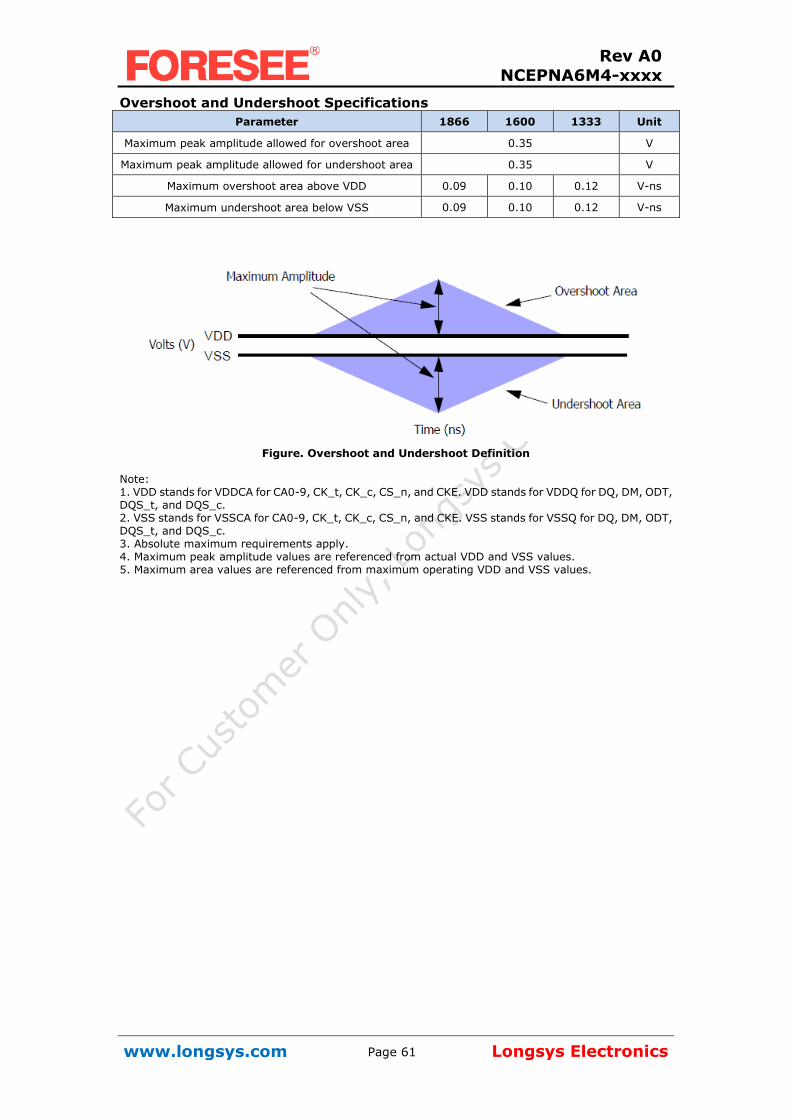
Overshoot and Undershoot Specifications
Parameter 1866 1600 1333 Unit
Maximum peak amplitude allowed for overshoot area 0.35 V
Maximum peak amplitude allowed for undershoot area 0.35 V
Maximum overshoot area above VDD 0.09 0.10 0.12 V-ns
Maximum undershoot area below VSS 0.09 0.10 0.12 V-ns
Figure. Overshoot and Undershoot Definition
Note: 1. VDD stands for VDDCA for CA0-9, CK_t, CK_c, CS_n, and CKE. VDD stands for VDDQ for DQ, DM, ODT, DQS_t, and DQS_c. 2. VSS stands for VSSCA for CA0-9, CK_t, CK_c, CS_n, and CKE. VSS stands for VSSQ for DQ, DM, ODT, DQS_t, and DQS_c. 3. Absolute maximum requirements apply. 4. Maximum peak amplitude values are referenced from actual VDD and VSS values. 5. Maximum area values are referenced from maximum operating VDD and VSS values.

Rev A0
NCEPNA6M4-xxxx
www.longsys.com Longsys Electronics Page 62
Output Buffer Characteristics
HSUL_12 Driver Output Timing Reference Load These ‘Timing Reference Loads’ are not intended as a precise representation of any particular system environment or a depiction of the actual load presented by a production tester. System designers should use IBIS or other simulation tools to correlate the timing reference load to a system environment. Manufacturers correlate to their production test conditions, generally one or more coaxial transmission lines terminated at the tester electronics.
Note:
1. All output timing parameter values (like tDQSCK, tDQSQ, tQHS, tHZ, tRPRE etc.) are reported with respect to this
reference load.
This reference load is also used to report slew rate.
Figure. HSUL_12 Driver Output Reference Load for Timing and Slew Rate
RONPU and RONPD resistor Definition
Note 1: This is under the condition that RONPD is turned off
Note 1: This is under the condition that RONPU is turned off
Figure. Output Driver: Definition of Voltages and Currents
RONPU and RONPD Characteristics with ZQ Calibration

Rev A0
NCEPNA6M4-xxxx
www.longsys.com Longsys Electronics Page 63
Output driver impedance RON is defined by the value of the external reference resistor RZQ. Nominal RZQ is 240Ω.
For example, with MMPUPD(max) = 15% and RONPD = 0.85, RONPU must be less than 1.0.
6. Output driver strength measured without ODT.

Rev A0
NCEPNA6M4-xxxx
www.longsys.com Longsys Electronics Page 64
RZQ I-V Curve
Figure. I-V Curve After ZQ Reset
Figure. I-V Curve After Calibration

Rev A0
NCEPNA6M4-xxxx
www.longsys.com Longsys Electronics Page 65
ODT Levels and I-V Characteristics On-Die Termination effective resistance, RTT, is defined by mode register MR11[1:0]. ODT is applied to the DQ, DM,and DQS_t/DQS_c pins. A functional representation of the on-die termination is shown in the figure below. RTT is defined by the following formula: RTTPU = (VDDQ - VOut) / | IOut |
Table. ODT DC Electrical Characteristics, assuming RZQ = 240 ohm after proper ZQ calibration
RTT(ohm) VOUT(V) IOUT
Min(mA) Max(mA)
RZQ/1 0.6 -2.17 -2.94
RZQ/2 0.6 -4.34 -5.88
RZQ/4 0.6 -8.68 -11.76
Rev A0
NCEPNA6M4-xxxx
www.longsys.com Longsys Electronics Page 66
CA and CS_n Setup, Hold and Derating For all input signals (CA and CS_n) the total tIS (setup time) and tIH (hold time) required is calculated by adding the data sheet tIS(base) and tIH(base) value to the and derating value respectively. Example: tIS (total setup time) = tIS(base) + △tIS
Setup (tIS) nominal slew rate for a rising signal is defined as the slew rate between the last crossing of VREF(DC) and the first crossing of VIH(AC)min. Setup (tIS) nominal slew rate for a falling signal is defined as the slew rate between the last crossing of VREF(DC) and the first crossing of VIL(AC)max. If the actual signal is always earlier than the nominal slew rate line between shaded `VREF(DC) to ac region', use nominal slew rate for derating value. If the actual signal is later than the nominal slew rate line anywhere between shaded `VREF(DC) to ac region', the slew rate of a tangent line to the actual signal from the ac level to dc level is used for derating value. Hold (tIH) nominal slew rate for a rising signal is defined as the slew rate between the last crossing of VIL(DC)max and the first crossing of VREF(DC). Hold (tIH) nominal slew rate for a falling signal is defined as the slew rate between the last crossing of VIH(DC)min and the first crossing of VREF(DC). If the actual signal is always later than the nominal slew rate line between shaded `DC to VREF(DC) region', use nominal slew rate for derating value. If the actual signal is earlier than the nominal slew rate line anywhere between shaded `DC to VREF(DC) region', the slew rate of a tangent line to the actual signal from the dc level to VREF(DC) level is used for derating value. For a valid transition the input signal has to remain above/below VIH/IL(AC) for some time tVAC. Although for slow slew rates the total setup time might be negative (i.e. a valid input signal will not have reached VIH/IL(AC) at the time of the rising clock transition) a valid input signal is still required to complete the transition and reach VIH/IL(AC). For slew rates in between the values listed in Table, the derating values may obtained by linear interpolation.These values are typically not subject to production test. They are verified by design and characterization.
Table. CA Setup and Hold Base-Values
Unit[ps] LPDDR3
1866
LPDDR3
1600
LPDDR3
1333 Reference
tIS(base) 75 100 VIH/L(AC)=VREF(DC)+/-150mV
tIS(base) 62.5 VIH/L(AC)=VREF(DC)+/-135mV
tIH(base) 80 100 125 VIH/L(AC)=VREF(DC)+/-100mV
Note 1: AC/DC referenced for 2V/ns CA slew rate and 4V/ns differential CK_t/CK_c slew rate.
Table. CS_n Setup and Hold Base-Values
Unit[ps] LPDDR3
1866
LPDDR3
1600
LPDDR3
1333 Reference
tIS(base) 195 215 VIH/L(AC)=VREF(DC)+/-150mV
tIS(base) 162.5 VIH/L(AC)=VREF(DC)+/-135mV
tIH(base) 180 220 240 VIH/L(AC)=VREF(DC)+/-100mV
Note 1: AC/DC referenced for 2V/ns CS_n slew rate and 4V/ns differential CK_t/CK_c slew rate.

Rev A0
NCEPNA6M4-xxxx
www.longsys.com Longsys Electronics Page 67
AC TIMING PARAMETERS (1/5)
Parameter Symbol min max
LPDDR3 1333
Unit
Maximum clock Frequency 667 MHz
Average Clock Period tCK(avg) min 1.5
ns max 100
Average high pulse width tCH(avg) min 0.45
tCK(avg) max 0.55
Average low pulse width tCL(avg) min 0.45
tCK(avg) max 0.55
Absolute Clock Period tCK(abs) min tCK(avg)min + tJIT(per)min ns
Absolute clock HIGH pulse width (with allowed jitter)
tCH(abs), allowed
min 0.43 tCK(avg)
max 0.57
Absolute clock LOW pulse width (with allowed jitter)
tCL(abs), allowed
min 0.43 tCK(avg)
max 0.57
Clock Period Jitter (with allowed jitter) tJIT(per), allowed
min -80 ps
max 80
Maximum Clock Jitter between two consecutive clock cycles (with allowed jitter)
tJIT(cc), allowed
max 160 ps
Duty cycle Jitter (with allowed jitter) tJIT(duty),
allowed
min
min((tCH(abs)min -
tCH(avg)min), (tCL(abs)min -
tCL(avg)min)) * tCK(avg)
max
max((tCH(abs)max -
tCH(avg)max), (tCH(abs)max -
tCL(avg)max)) * tCK(avg)
Cumulative error across 2 cycles tERR(2per),
allowed
min -118 ps
max 118
Cumulative error across 3 cycles tERR(3per),
allowed
min -140 ps
max 140
Cumulative error across 4 cycles tERR(4per),
allowed
min -155 ps
max 155
Cumulative error across 5 cycles tERR(5per),
allowed
min -168 ps
max 168
Cumulative error across 6 cycles tERR(6per),
allowed
min -177 ps
max 177
Cumulative error across 7 cycles tERR(7per),
allowed
min -186 ps
max 186
Cumulative error across 8 cycles tERR(8per),
allowed
min -193 ps
max 193
Cumulative error across 9 cycles tERR(9per)
allowed
min -200 ps
max 200
Cumulative error across 10 cycles tERR(10per)
allowed
min -205 ps
max 205
Rev A0
NCEPNA6M4-xxxx
www.longsys.com Longsys Electronics Page 68
AC TIMING PARAMETERS (2/5)
Parameter Symbol min max
LPDDR3 1333
Unit
Clock Timing (continued)
Cumulative error across 11 cycles tERR(11per),
allowed
min -210 ps
max 210
Cumulative error across 12 cycles tERR(12per),
allowed
min -215 ps
max 215
Cumulative error across n cycles
(n = 13, 14 ,. . . ,20)
tERR(nper),
allowed
min
tERR(nper),allowed min = (1
+ 0.68ln(n)) *
tJIT(per),allowed min ps
max
tERR(nper),allowed max = (1
+ 0.68ln(n)) *
tJIT(per),allowed max
ZQ Calibration Parameters
Initialization Calibration Time tZQINIT min 1 us
Long Calibration Time tZQCL min 360 ns
Short Calibration Time tZQCS min 90 ns
Calibration Reset Time tZQRESET min max(50ns, 3nCK) ns
Read Parameters
DQS output access time from CK/CK# tDQSCK min 2.5
ns max 2.5
DQSCK Delta short tDQSCKDS max 265 ps
DQSCK Delta Medium tDQSCKDM max 593 ps
DQSCK Delta Long tDQSCKDL max 733 ps
DQS-DQ skew tDQSQ max 165 ps
DQS Output High Pulse Width tQSH min tCH(abs) - 0.05 tCK(avg)
DQS Output Low Pulse Width tQSL min tCL(abs) - 0.05 tCK(avg)
DQ/DQS output hold time from DQS tQH min MIN (tQSH, tQSL) ps
Read preamble tRPRE min 0.9 tCK(avg)
Read postamble tRPST min 0.3 tCK(avg)
DQS low-Z from clock tLZ(DQS) min tDQSCK(min) - 300 ps
DQ low-Z from clock tLZ(DQ) min tDQSCK(min) - 300 ps
DQS high-Z from clock tHZ(DQS) max tDQSCK(max) - 100 ps
DQ high-Z from clock tHZ(DQ) max tDQSCK(max) + (1.4 x
tDQSQmax) ps

Rev A0
NCEPNA6M4-xxxx
www.longsys.com Longsys Electronics Page 69
AC TIMING PARAMETERS (3/5)
Parameter Symbol min max
LPDDR3 1333
Unit
Write Parameters
DQ and DM input setup time (Vref based) tDS min 175 ps
DQ and DM input hold time (Vref based) tDH min 175 ps
DQ and DM input pulse width tDIPW min 0.35 tCK(avg)
Write command to 1st DQS latching
transition tDQSS
min 0.75 tCK(avg)
max 1.25
DQS input high-level width tDQSH min 0.4 tCK(avg)
DQS input low-level width tDQSL min 0.4 tCK(avg)
DQS falling edge to CK setup time tDSS min 0.2 tCK(avg)
DQS falling edge hold time from CK tDSH min 0.2 tCK(avg)
Write postamble tWPST min 0.4 tCK(avg)
Write preamble tWPRE min 0.8 tCK(avg)
CKE Input Parameters
CKE min. pulse width (high/low pulse width) tCKE min max(7.5ns, 3nCK) ns
CKE input setup time tISCKE min 0.25 tCK(avg)
CKE input hold time tIHCKE min 0.25 tCK(avg)
Command path disable delay tCPDED min 2 tCK(avg)
Command Address Input Parameters
Address and control input setup time tISCA min 175 ps
Address and control input hold time tIHCA min 175 ps
CS_n input setup time tISCS min 290 tCK(avg)
CS_n input hold time tIHCS min 290 tCK(avg)
Address and control input pulse width tIPWCA min 0.35 tCK(avg)
CS_n input pulse width tIPWCS min 0.7 tCK(avg)
Boot Parameters (10MHz-55MHz)
Clock Cycle Time tCKb min 18
ns max 100
CKE Input Setup Time tISCKEb min 2.5 ns
CKE Input Hold Time tIHCKEb min 2.5 ns
Address & Control Input Setup Time tISb min 1150 ps
Address & Control Input Hold Time tIHb min 1150 ps
DQS Output Data Access Time from CK/CK# tDQSCKb min 2.0
ns max 10.0
Data Strobe Edge to Output Data Edge
tDQSQb tDQSQb min 1.2 ns
Mode Register Parameters
MODE REGISTER Write command period tMRW min 10 tCK(avg)
MODE REGISTER Read command period tMRR min 4 tCK(avg)
Additional time after tXP has expired until
MRR command may be issued tMRRI min tRCD(MIN) ns

Rev A0
NCEPNA6M4-xxxx
www.longsys.com Longsys Electronics Page 70
AC TIMING PARAMETERS (4/5)
Parameter Symbol min max
LPDDR3 1333
Unit
Core Parameters
Read Latency RL min 10 tCK(avg)
Write Latency (Set A) WL min 6 tCK(avg)
Write Latency (Set B) WL min 8 tCK(avg)
ACTIVE to ACTIVE command period tRC min
tRAS+tRPab
(with all-bank Precharge)
tRAS+tRPpb
(with per-bank Precharge)
ns
CKE min. pulse width during Self-Refresh
(low pulse width during Self-Refresh) tCKESR min max(15ns, 3nCK) ns
Self refresh exit to next valid command delay tXSR min max(tRFCab +10ns, 2nCK) ns
Exit power down to next valid command
delay tXP min max(7.5ns, 3nCK) ns
CAS to CAS delay tCCD min 4 tCK(avg)
Internal Read to Precharge command delay tRTP min max(7.5ns, 4nCK) ns
RAS to CAS Delay tRCD min max(18ns, 3nCK) ns
Row Precharge Time (single bank) tRPpb min max(18ns ,3nCK) ns
Row Precharge Time (all banks) - 8-bank tRPab min max(21ns, 3nCK) ns
Row Active Time tRAS min max(42ns, 3nCK)
ns max 70,000
Write Recovery Time tWR min max(15ns, 4nCK) ns
Internal Write to Read Command Delay tWTR min max(7.5ns, 4nCK) ns
Active bank A to Active bank B tRRD min max(10ns, 2nCK) ns
Four Bank Activate Window tFAW min max(50ns, 8nCK) ns
Minimum Deep Power Down Time tDPD min 500 us
ODT Parameters
Asynchronous RTT turn-on dely from ODT
input tODTon
min 1.75 ns
max 3.5
Asynchronous RTT turn-off delay from ODT
input tODToff
min 1.75 ns
max 3.5
Automatic RTT turn-on delay after READ data tAODTon max tDQSCKmax + 1.4 * tDQSQmax
+ tCK(avg,min) ps
Automatic RTT turn-off delay after READ data tAODToff min tDQSCKmin - 300 ps
RTT disable delay from power down,
self-refresh and deep power down entry tODTd min 12 ns
RTT enable delay from power down and self
refresh exit tODTe max 12 ns

Rev A0
NCEPNA6M4-xxxx
www.longsys.com Longsys Electronics Page 71
AC TIMING PARAMETERS (5/5)
Parameter Symbol min max
LPDDR3 1333
Unit
CA Training Parameters
First CA calibratino command after CA
calibration mode is programmed tCAMRD min 20 tCK(avg)
First CA calibratino command after CKE is
LOW tCAENT min 10 tCK(avg)
CA calibration exit command after CKE is
HIGH tCAEXT min 10 tCK(avg)
CKE LOW after CA calibration mode is
programmed tCACKEL min 10 tCK(avg)
CKE HIGH after the last CA calibration
results are driven tCACKEH min 10 tCK(avg)
Data out delay after CA training
calibration command is programmed tADR max 20 ns
MRW CA exit command to DQ tri-state tMRZ min 3 ns
CA calibration command to CA calibration
command delay tCACD min RU(tADR+2*tCK) tCK(avg)
Write Leveling Parameters
DQS_t/DQS_c delay after write leveling
mode is programmed tWLDQSEN
min 25 ns
max -
First DQS_t/DQS_c edge after write
leveling mode is programmed tWLMRD
min 40 ns
max -
Write leveling output delay tWLO min 0
ns max 20
Write leveling hold time tWLH min 205 ps
Write leveling setup time tWLS min 205 ps
Mode register set command delay tMRD min Max(14ns, 10nCK)
ns max
Temperature De-Rating
tDQSCK De-Rating tDQSCK
(Derated) max 5620
Core Timings Temperature De-Rating
tRCD(Derate
d) min tRCD + 1.875
tRC(Derated
) min tRC + 1.875
tRAS(Derate
d) min tRAS + 1.875
tRP(Derated) min tRP + 1.875
tRRD(Derate
d) min tRRD + 1.875