emc review for belle ii (grounding & shielding plans) sub-systems ( xxxxx)
TRANSCRIPT
EMC review for Belle II (Grounding & shielding plans)
Sub-systems ( XXXXX)

Outline
• 1. Introduction • 2. Grounding strategy
–2.1. Implementations aspects• 3. Noise emission issues
–Test plans• 4. Noise immunity issues
–Test plans• 5. Cabling• 6.Conclusions

1. Introduction
• Short description and schematic of each subdetector.

2. Grounding strategy• Outline of the grounding strategy
– Information about current or previous grounding topology.• Single point, multipoint or other
– Describe the actual or proposed grounding topology • Place a conceptual schematic.
– Implementation • Electro-mechanical schematic• Type of grounding connection Bonding or straps?• Capacitors connections ?• …….
• Nest slides shows as an example some of this schematics for PXD system

2. Grounding strategy - Topology
Single-point
Only for low level and low frequency circuits (below 1 MHz)
Multi-pointFor high level frequency circuits (above 1 MHz)
It prevents excessive radiated emissions and maintains low impedanceBetter filter performance
PXD is very small but the FE Amplifier bandwidth is around100 MHz
Hybrid ground topology is the preferred option as FE amplifier bandwidth is very high – 100 MHz
HybridEquivalent to
Multi-point
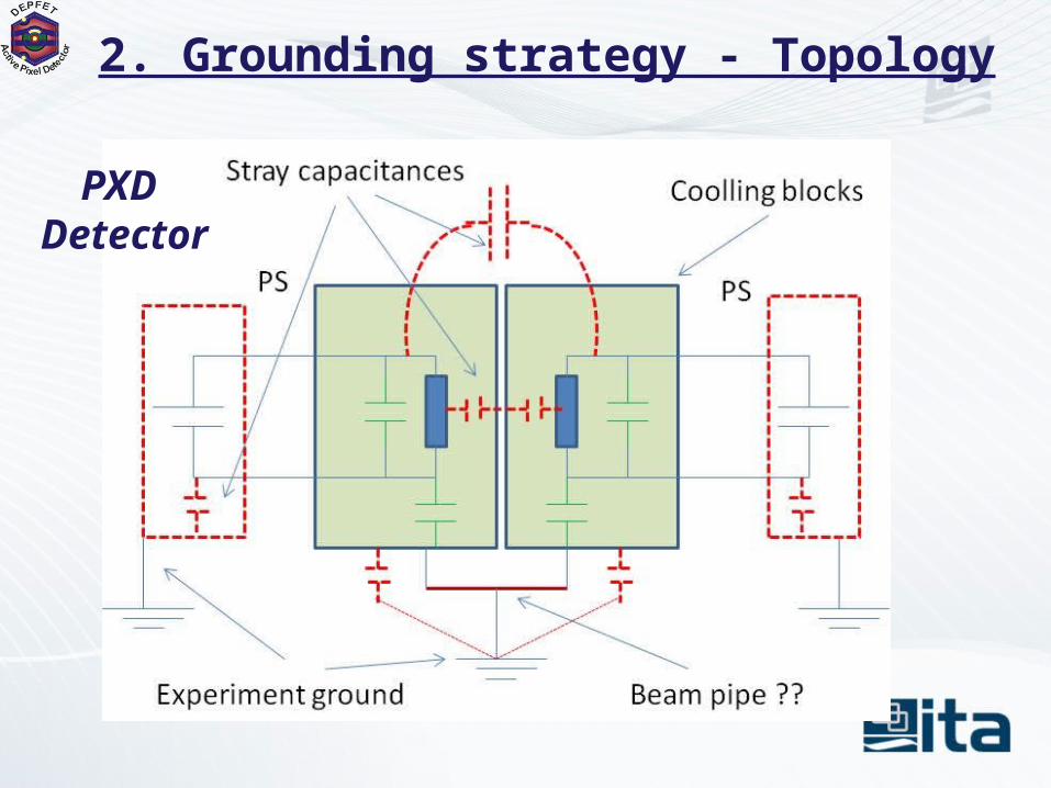
2. Grounding strategy - Topology
PXD Detector
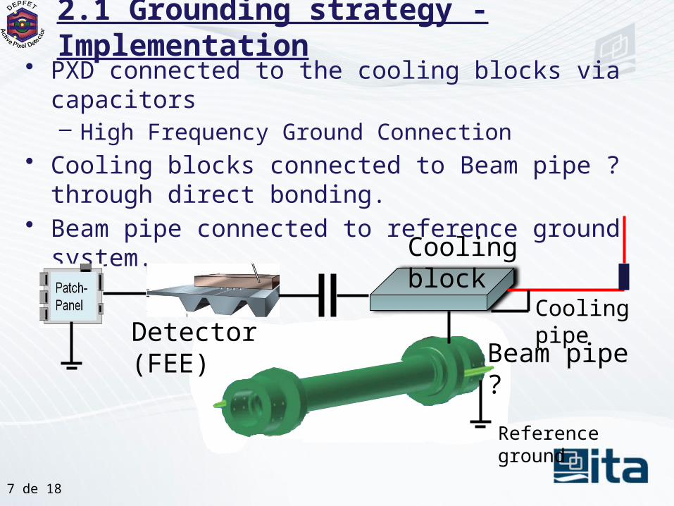
• PXD connected to the cooling blocks via capacitors – High Frequency Ground Connection
• Cooling blocks connected to Beam pipe ? through direct bonding.
• Beam pipe connected to reference ground system.
7 de 18
2.1 Grounding strategy - Implementation
Detector (FEE)
Cooling block
Beam pipe ?
Reference ground
Cooling pipe

3. Noise emission issues• Emission issues.
– Analysis of the main noise sources• Identification
– Power supplies, slow control system or any other ???• Test plans
• Remark or comment the main noise sources for the subsystem– Type of noise
• Conducted or radiated ?– Frequency – Possible coupling path
• Test plans .– Noise emissions test plans ?– Show test results in case they have been already
performed.

4. Noise immunity issues• Analysis of the main noise victims
– Identification • Describe the signal detection circuit (Detector – FEE )
• Schematic• Frequency range where detector circuit expect to be
sensitive.• Possible coupling path
• Describe any other sensitive circuit you expect noise problems
• Test plans .– Noise immunity test plans ?
• Show test results in case they have been already performed.
• Sensitive• Nest slides shows as an example some schematics
of detection circuit for PXD system

Vsource
Vamplow
S
DG
CG
Clear
Pixel
DCD
Zin (Z??)
Signal
Signal Return
4. Noise immunity issues – Signal circuit

),( sdsource LCfZ iIs
),( sdamplow LCfZ
iAmplowI
sourceV
AmplowV
cableZ
logAnaGND
.: AmpSoGndZ
),,( fBAfV loopinduced 4. Noise immunity issues – Signal circuit
Signal circuit: PXD

5. Cabling• Cabling and Shielding aspects
– Type of cables ?– cabling layout ?– Cable connections ?– Grounding of cooling pipes ?– Any other relevant information

6. Conclusions