emc and wireless systems - wayne state universityapandya/seminars/index_files/wsu - marc… · emc...
TRANSCRIPT

EMC and Wireless Systems
EMC and Wireless Systems
• Antenna basics and transmission lines.
• EMC of Electronic Modules.
• Communication channel parameters.
• EMC of communication systems.
• EMC Challenges / opportunities for the
future.
1
EMC and Wireless Systems
Wireless System Antennas
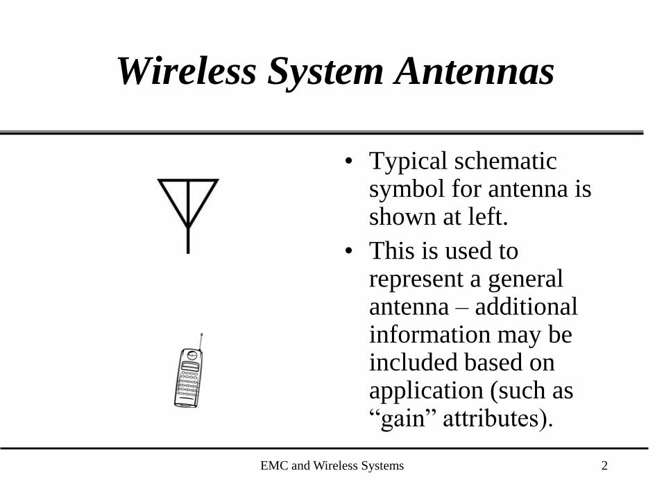
• Typical schematic symbol for antenna is shown at left.
• This is used to represent a general antenna – additional information may be included based on application (such as “gain” attributes).
2

EMC and Wireless Systems
Antenna Purpose
• The antenna is connected to the end of the
transmission line.
• Antenna is the method to transfer energy from the
transmitter/receiver to the “medium” (air).
3

EMC and Wireless Systems
Antenna Basics
• Most wireless system
antennas are designed
to utilize the electric
field component of
E/M wave for
communication.
• This type of antenna
can be represented as
an “open” capacitor.
4

EMC and Wireless Systems
Antenna Performance
• Antenna performance is generally a “reciprocal”
process – if the antenna works well to transmit a
signal, it will work well on receiving a signal.
5

EMC and Wireless Systems
Electrical and Physical Size
• Many antennas are
physically constructed
to be a specific length
corresponding to the
signal wavelength.
• Typical antennas are
multiples of ¼ of a
wavelength, for
“resonant” conditions.
6

EMC and Wireless Systems
Electrical Model of Antenna
Parameters
• An antenna can be represented just like any other
type of electrical component.
• Can be expressed as a complex impedance load:
Zant = Rr + jX (ohms)
Where:
Rr is the “Radiation Resistance” (a derived value describing how
effective the antenna is in transferring power to/from the medium)
jX is the value of the sum of the reactance (due to series inductance
and capacitance).
7

EMC and Wireless Systems
Description of Antenna
Parameters
• Rr of ¼ wavelength antenna (typically
called a monopole) is about 37 ohms.
• Antenna reactance is the “jX”, and is the
same as a series resonant circuit.
– When the antenna length is physically shorter
than ¼ wavelength, jX is negative and antenna
“looks” capacitive.
– When “jX = 0” the antenna is “resonant”.
8

EMC and Wireless Systems
Antenna / Transmitter
Interface
• Antenna (“E-field” antenna shown) is connected
to the transmitter via a transmission line.
• Objective is to send/receive power/signal with
minimal loss from/to transmitter/receiver.
9
EMC and Wireless Systems
Transmission Line Types
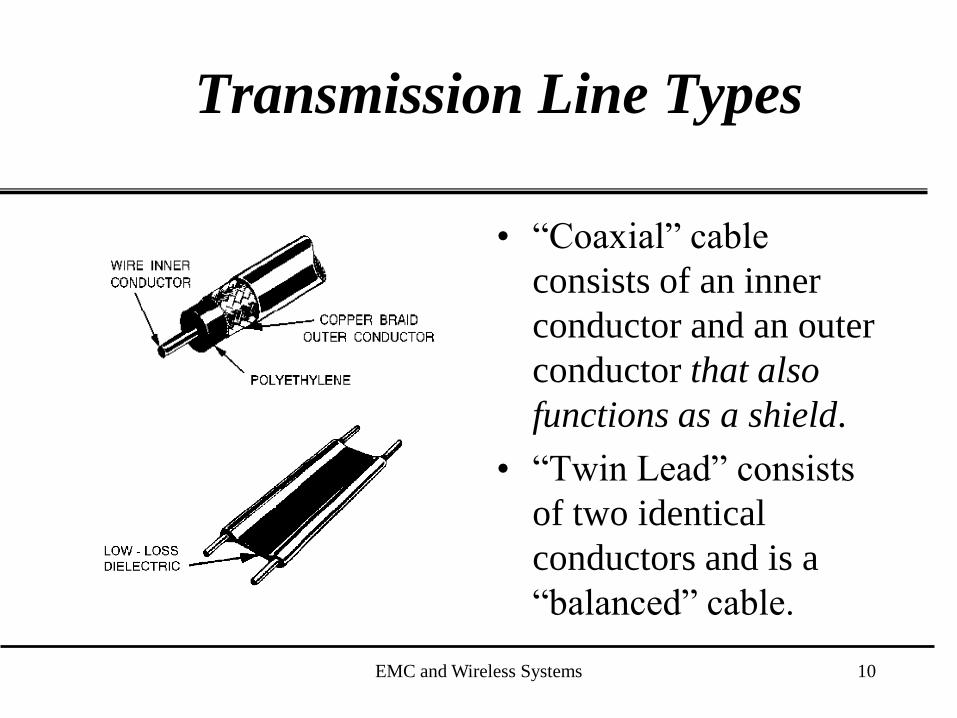
• “Coaxial” cable
consists of an inner
conductor and an outer
conductor that also
functions as a shield.
• “Twin Lead” consists
of two identical
conductors and is a
“balanced” cable.
10
EMC and Wireless Systems
Transmission Line Model
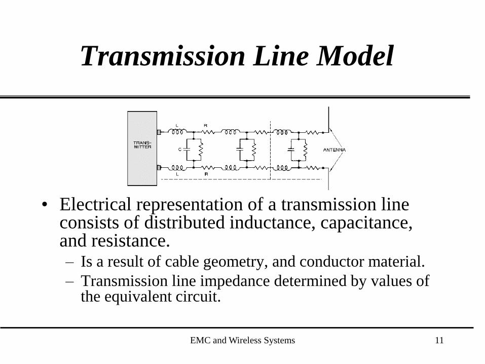
• Electrical representation of a transmission line consists of distributed inductance, capacitance, and resistance.– Is a result of cable geometry, and conductor material.
– Transmission line impedance determined by values of the equivalent circuit.
11

EMC and Wireless Systems
Transmission Line Metrics
• Transmission lines are characterized in terms of
impedance, and is a function of a per-unit length
of inductance (L), capacitance (C), and resistance.
– A simplified expression for impedance is (neglecting
resistance of the conductors) is Z = (L/C)1/2.
– Note that Z does not depend on the length of line.
• Example: RG-58 cable has a specified capacitance
of 23 pf/ft , Z= 50 ohms, and “TV Twin lead” has
a specified capacitance of 4.5 pf / ft, Z=300 ohms.
12

EMC of Electronic Modules
• Early boards used
“stick lead”
components - now use
many surface mount
devices (SMD).
• Conductors are created
by on the surface of
the printed (PCB)
circuit board layers.
13EMC and Wireless Systems

PCB Properties – “Parasitics”
• Every conductor (“trace”) on a PCB has real
characteristics of:
– Resistance: Determine by trace conductivity.
– Capacitance: Determined by spacing to other
traces and dielectric of board.
– Inductance: Determined by the geometry of the
current loop.
14EMC and Wireless Systems

PCB Properties - Capacitance
• Traces have coupling due to electric fields.
• Maximum coupling occurs between largest areas
(“plates of a capacitor”).
• Largest area typically called “Ground Plane”.
15EMC and Wireless Systems

PCB Properties - Inductance
• Energy is stored in magnetic field around
conductor.
• Magnetic Flux lines can couple to adjacent
conductors (similar to a transformer).
• Trace length and width determines the
geometry of the flux lines (determines the
current loop area).
16EMC and Wireless Systems

Representation of PCB Parasitic
Inductance and Capacitance
• Inner and outer layer traces can have coupling to
each other.
• Current return planes may be placed on the outside
of the board.
17EMC and Wireless Systems

PCB Trace Transmission Line
Model
• A “transmission line” is represented by any pair of
wires or conductors.
• Goal is to characterize impedance of line.
18EMC and Wireless Systems

Current Paths on PCB’s
• All currents return to their source.
• PCB traces exhibit impedance (R + jX).
• Current Paths:
– At low frequency - path of least R.
– At high frequency – path of least Z.
• For traces containing high frequency
located over a return plane – current return
minimizes loop inductance.19EMC and Wireless Systems

Typical PCB Parasitic Values
• Capacitance between traces/conductors:
– Approximately 3 pF / inch.
– Dependent upon trace separation.
• Inductance of a trace:
– Approximately 15 nH / inch.
– Can vary by ½ to 2 times, dependent upon
current loop geometry.
20EMC and Wireless Systems

PCB “Crosstalk”
• Occurs when energy from traces couple to other traces.
• May be due to capacitance, inductance, or combination of both.
– Capacitance coupling result of parallel traces.
– Inductive coupling result of trace loops in same planes.
• Can occur from same layer, or different layers.
21EMC and Wireless Systems

Components and PCB’s
• “Ideal” and “Real” components may have very
different characteristics in high speed circuits.
• Traditional resistor (shown below) is represented
by only resistance.
22EMC and Wireless Systems
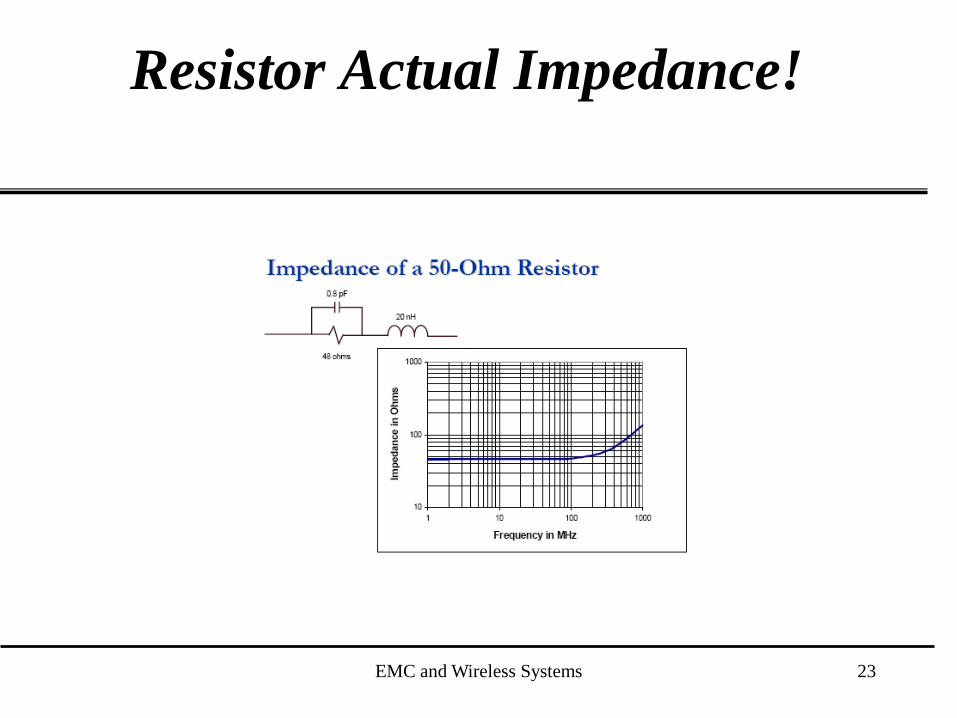
Resistor Actual Impedance!
23EMC and Wireless Systems

Components and PCB’s
• “Ideal” and “Real” components may have very
different characteristics in high speed circuits.
• Traditional capacitor (shown below) is represented
by only capacitance.
24EMC and Wireless Systems

Capacitor Actual Impedance!
25EMC and Wireless Systems

Components and PCB’s
• “Ideal” and “Real” components may have very
different characteristics in high speed circuits.
• Traditional inductor (shown below) is represented
by only inductance.
26EMC and Wireless Systems

Inductor Actual Impedance!
27EMC and Wireless Systems

PCB Design – Power Distribution
• Critical part of PCB is the ability to supply
required power to circuit.
• Digital device switching process can have
significant power/current demands.
• Switching currents can have high speed
content.
• Important to supply required current in
required time.28EMC and Wireless Systems

PCB Power Distribution
• Power distribution system consists of three (3) main sections:
– A – The power source.
– B – The parasitic capacitance.
– C – The parasitic inductance.
29EMC and Wireless Systems

PCB Power Supply
Decoupling
• Goal is to be able to provide power when required,
for the time required.
• If power source is located away from digital
device, series inductance may be too high.
• Solution is to locate energy storage devices
(capacitors) physically near devices requiring
energy.
• Locating capacitors is known as “decoupling”.
30EMC and Wireless Systems

PCB Summary
• PCB is a critical part of electronic systems
and it’s design / layout issues can:
– Affect system functionality.
– Prevent meeting signal processing requirements
(“Signal Integrity”).
– Result in not meeting EMC requirements.
31EMC and Wireless Systems

PCB Summary - Continued
• Component selection and placement
important to PCB’s performance:
– Not all components are created equal!
– Need to understand component parasitic
elements.
• Proper attention to both PCB AND
COMPONENT SELECTION can help
assure a successful product!
32EMC and Wireless Systems

EMC and Wireless Systems
Communication Channels
• Three (3) types of propagation can occur: (1) Surface (ground), (2) Reflection (sky wave), (3) Space wave (line of sight).
• Each type is typically a function of signal frequency (highest frequencies are line of sight).
33

EMC and Wireless Systems
E/M Wave “Polarization”
• Transmitter and
receiver antenna
polarization refers to
the E field vector
orientation.
• A monopole on a
typical wireless device
uses vertical
polarization.
34

EMC and Wireless Systems
Electromagnetic Frequency
Bands
• Much of today’s communication occurs from MF to UHF.
• MF/VHF/UHF used for broadcasting.
• UHF is used for handheld and mobile devices (phones, Wi-Fi).
35

EMC and Wireless Systems
Communication “Link
Budget”
• The “link budget” determines the received-signal power for a line-of-sight communication link:
Pt + Gt – L + Gr = PrWhere:
Pt = Signal power at transmitter output, in dBm
Gt = Transmitter antenna gain, in dBi
L = Propagation loss, dB
Gr = Receiver antenna gain, in dBi
Pr = Signal power at the receiver input, in dBm
36

EMC and Wireless Systems
Free-Space Propagation Loss
(“Friis”) Equation
• Allows determination of the expected minimum
propagation path loss for “free space” conditions.
• Propagation Loss (in dB) = 20 log (4p r / l)
Where: r = distance, l = signal wavelength
37

EMC and Wireless Systems
“Rayleigh Effects” on
Propagation Loss
• The communication path can be significantly affected by
objects in the line-of-sight.
• Typically expressed as: dB = 40 + n log (r), where r is the
path distance, n is a function of wavelength.
38

EMC and Wireless Systems
Comparison of Friis to
Rayleigh Effects
• For a transmitter / receiver system operating on 2.4 GHz, and with a range of about 5 km in free-space, due to Rayleigh Effects, this same signal would have a range of about 226 meters!– Typical path loss impact due to various objects:
• Trees, 10 to 20 dB
• Walls, 10 to 15 dB
• Floors, 10 to 30 dB
• Therefore, it is important to understand when to apply Free-Space or Rayleigh conditions to determine communication link performance.
39

EMC and Wireless Systems
• Digital systems can provide robustness to EMC issues in the communication link by error detection and correction methods as well a through bit-error-rate (BER) parameters.
• If a higher BER can be accommodated, this may allow minimal link budget values.
• Goal is an acceptable balance of transmitter / receiver specifications (such as sensitivity, signal to noise ratio), path loss, and BER.
Benefit of Digital Modulation
Methods
40

EMC and Wireless Systems
“EMC” of Communication
Systems
• The EMC of communication systems can be
significant due to the “coexistence” challenges.
• Low level signals from distant devices may be not
be received and high power systems may interfere.
41

EMC and Wireless Systems
Impact Upon “Link Budget”
• Link budget
calculations can be
significantly affected
by interference
sources.
• Can affect both the
“channel” and the
receiver performance.
42

EMC and Wireless Systems
Wireless System EMC - Summary
• The proliferation of wireless systems can result (ironically) in the demand for more immune/robust systems.
• System compatibility can be evaluated by understanding the basics of EMC as applied to other technologies.
• By understanding how antennas, transmission lines, and electromagnetic fields interact, the analysis of wireless system EMC can be accomplished.
43

Methods to Assure EMC
• EMC testing may
be conducted on
any systems
containing
electrical/electronic
components
(photos courtesy of
ETS-Lindgren).
EMC and Wireless Systems 44

Applications of EMC Testing
• EMC testing may be done on any size
component or system.
• EMC is important for systems designed for
space exploration…..and…EMC and Wireless Systems 45

..EMC Is Important for Earth
Based Systems!
EMC and Wireless Systems 46

EMC and Wireless Systems
EMC Challenges and
Opportunities For The Future
• Understand the system’s intended use, application, parameters, and specifications.
• Perform an evaluation of system location with other devices present (and future plans).
• Know the applicable standards and regulations.
• In summary: An understanding of the basics of E/M and technology can provide the key to an effective and efficient EMC program that will enhance a product’s reputation and performance!
47