em4100 transponder
TRANSCRIPT

EM4100
Copyright 2002, EM Microelectronic-Marin SA 1 www.emmicroelectronic.com
Read Only Contactless Identification DeviceDescriptionThe EM4100 (previously named H4100) is a CMOSintegrated circuit for use in electronic Read Only RFTransponders. The circuit is powered by an external coilplaced in an electromagnetic field, and gets its masterclock from the same field via one of the coil terminals. Byturning on and off the modulation current, the chip willsend back the 64 bits of information contained in a factor ypre-programmed memory array.The programming of the chip is performed by laser fusingof polysilicon links in order to store a unique code on eachchip.The EM4100 has several metal options which are used todefine the code type and data rate. Data rates of 64, 32and 16 periods of carrier frequency per data bit areavailable. Data can be coded as Manchester, Biphase orPSK.Due to low power consumption of the logic core, no supplybuffer capacitor is required. Only an external coil isneeded to obtain the chip function. A parallel resonancecapacitor of 74 pF is also integrated.
Features� 64 bit memory array laser programmable� Several options of data rate and coding available� On chip resonance capacitor� On chip supply buffer capacitor� On chip voltage limiter� Full wave rectifier on chip� Large modulation depth due to a low impedance
modulation device� Operating frequency 100 - 150 kHz� Very small chip size convenient for implantation� Very low power consumption
Applications� Logistics automation� Anticounterfeiting� Access control� Industrial transponder
Typical Operating Configuration
Coil1
Coil2
EM4100
L: typical 21.9mH for fo = 125kHz
Fig. 1
Pin Assignment
EM4100
COIL1COIL2
VDDVSS
COIL1 Coil terminal / Clock inputCOIL2 Coil terminal
Fig. 2
EM MICROELECTRONIC - MARIN SA

EM4100
Copyright 2002, EM Microelectronic-Marin SA 2 www.emmicroelectronic.com
Absolute Maximum RatingsParameter Symbol ConditionsMaximum DC Current forcedon COIL1 & COIL2
Power Supply
Storage Temp. Die formStorage Temp. PCB form
Electrostatic dischargemaximum to MIL-STD-883Cmethod 3015
ICOIL
VDD
TstoreTstore
VESD
±30mA
-0.3 to 7.5V
-55 to +200°C-55 to +125°C
1000V
Stresses above these listed maximum ratings may causepermanent damage to the device.Exposure beyond specified operating conditions max affectdevice reliability or cause malfunction.
Operating ConditionsParameter Symbol Min. Typ. Max. UnitsOperating Temp.
Maximum CoilCurrent
AC Voltage on Coil
Supply Frequency
Top
ICOIL
Vcoil
fcoil
-40
3
100
14*
+85
10
150
°C
mA
Vpp
kHz
*) The AC Voltage on Coil is limited by the on chip voltagelimitation circuitry. This is according to the parameter Icoil inthe absolute maximum ratings.
Handling ProceduresThis device has built-in protection against high staticvoltages or electric fields; however due to the uniqueproperties of this device, anti-static precautions should betaken as for any other CMOS component.
System Principle
AntennaDriverOscillator
DemodulatorFilterandGain
Data decoder Data receivedfrom transponder
Tranceiver Transponder
Coil1
Coil2
EM4100
Signal on coils
Transponder coil
Transeiver coil
RF Carrier Data
Fig. 3

EM4100
Copyright 2002, EM Microelectronic-Marin SA 3 www.emmicroelectronic.com
Electrical CharacteristicsVDD = 1.5V, VSS = 0V, fC1 = 134kHz square wave, Ta = 25°CVC1 = 1.0V with positive peak at VDD and negative peak at VDD -1V unless otherwise specified
Parameter Symbol Test Conditions Min. Typ. Max. UnitsSupply Voltage
Rectified Supply Voltage
Coil1 - Coil2 Capacitance
Power Supply Capacitor
VDD
VDDREC
Cres
Csup
VCOIL1 - VCOIL2 = 2.8 VDCModulator switch = “ON”Vcoil=100mVRMS f=10kHz
1.5
1.5
74 2)
120
1) V
V
pF
pFBiphase & ManchesterVersionsSupply Current
C2 pad Modulator ONvoltage drop
C1 pad Modulator ONvoltage drop
IDD
VONC2
VONC1
VDD=1.5V IVDDC2=100µA with ref. to VDDVDD=5.0V IVDDC2=1mA with ref. to VDD
VDD=5.0V IVDDC1=1mA with ref. to VDD
0.92.1
2.1
0.63
1.12.3
2.3
1.5
1.32.8
2.8
µA
VV
V
PSK VersionSupply Current PSK
C2 pad Modulator ONvoltage drop
IDDPSK
VONC2PSK VDD=1.5V IVDDC2=100µA with ref. to VDD 0.3
0.92
0.6
2
0.9
µA
V
Note 1) The maximum voltage is defined by forcing 10mA on COIL1 - COIL2Note 2) The tolerance of the resonant capacitor is ± 15% over the whole production. Optional reduced tolerance on request On a wafer basis, the tolerance is ± 2%
Timing CharacteristicsVDD = 1.5V, VSS = 0V, fcoil = 134kHz square wave, Ta = 25°CVC1 = 1.0V with positive peak at VDD and negative peak at VDD -1V unless otherwise specifiedTimings are derived from the field frequency and are specified as a number of RF periods.
Parameter Symbol Test Conditions Value Units
Read Bit Period Trdb depending on option 64, 32, 16 RF periods
Timing Waveforms
BIT n BIT n+1 BIT n+2
64, 32 or 16 TOC, depending on optionTOC
COIL1
Serial Data Out
Fig. 4

EM4100
Copyright 2002, EM Microelectronic-Marin SA 4 www.emmicroelectronic.com
Block Diagram
CLOCKEXTRACTOR
FULL WAVERECTIFIER
DATAMODULATOR
SEQUENCER
DATAENCODER
MEMORYARRAY
LogicClock
SerialData Out
ModulationControl
Cres
COIL1
COIL2
AC1
AC2
+
-
Csup
VDD
VSS
a
a: open only for PSK versionFig. 5
Functional DescriptionGeneralThe EM4100 is supplied by means of an electromagneticfield induced on the attached coil. The AC voltage isrectified in order to provide a DC internal supply voltage.When the last bit is sent, the chip will continue with the firstbit until the power goes off.
Full Wave RectifierThe AC input induced in the external coil by an incidentmagnetic field is rectified by a Graetz bridge. The bridgewill limit the internal DC voltage to avoid malfunction instrong fields.
Clock ExtractorOne of the coil terminals (COIL1) is used to generate themaster clock for the logic function. The output of the clockextractor drives a sequencer.
SequencerThe sequencer provides all necessary signals to addressthe memory array and to encode the serial data out.Three mask programmed encoding versions of logic areavailable. These three encoding types are Manchester,biphase and PSK. The bit rate for the first and the secondtype can be 64 or 32 periods of the field frequency. Forthe PSK version, the bit rate is 16.The sequencer receives its clock from the COIL1 clockextractor and generates every internal signal controllingthe memory and the data encoder logic.
Data ModulatorThe data modulator is controlled by the signal ModulationControl in order to induce a high current in the coil. In thePSK version, only COIL2 transistor drives this high current.In the other versions, both coil1 and coil2 transistors driveit to Vdd. This will affect the magnetic field according to thedata stored in the memory array.
Resonance CapacitorThis capacitor can be trimmed in factory by 0.5pf steps toachieve the absolute value of 74pf typically. This option,which is on request, allows a smaller capacitor toleranceon the whole of the production.
EM4100
Copyright 2002, EM Microelectronic-Marin SA 5 www.emmicroelectronic.com
Memory Array for Manchester & Bi-Phase encoding ICsThe EM4100 contains 64 bits divided in five groups ofinformation. 9 bits are used for the header, 10 row paritybits (P0-P9), 4 column parity bits (PC0-PC3), 40 data bits(D00-D93), and 1 stop bit set to logic 0.
1 1 1 1 1 1 1 1 1 9 header bits8 version bits or D00 D01 D02 D03 P0customer ID D10 D11 D12 D13 P1
D20 D21 D22 D23 P232 data bits D30 D31 D32 D33 P3
D40 D41 D42 D43 P4D50 D51 D52 D53 P5D60 D61 D62 D63 P6D70 D71 D72 D73 P7D80 D81 D82 D83 P8D90 D91 D92 D93 P9 10 line parityPC0 PC1 PC2 PC3 S0 bits
4 column parity bits
The header is composed of the 9 first bits which are allmask programmed to "1". Due to the data and parityorganisation, this sequence cannot be reproduced in thedata string. The header is followed by 10 groups of 4 databits allowing 100 billion combinations and 1 even rowparity bit. Then, the last group consists of 4 event columnparity bits without row parity bit. S0 is a stop bit which iswritten to "0"Bits D00 to D03 and bits D10 to D13 are customer specificidentification.These 64 bits are outputted serially in order to control themodulator. When the 64 bits data string is outputted, theoutput sequence is repeated continuously until power goesoff.
Memory Array for PSK encoding ICsThe PSK coded IC's are programmed with odd parity forP0 and P1 and always with a logic zero.The parity bits from P2 to P9 are even.The column parity PC0 to PC3 are calculated including theversion bits and are even parity bits.
Code Description
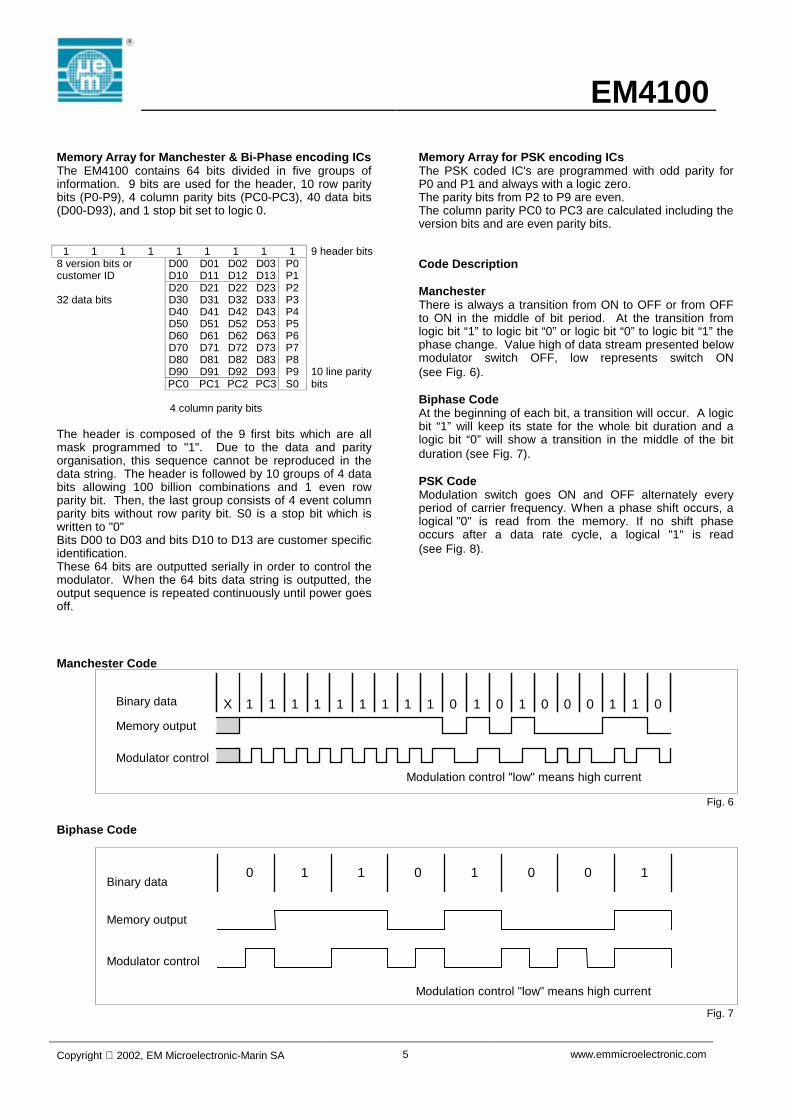
ManchesterThere is always a transition from ON to OFF or from OFFto ON in the middle of bit period. At the transition fromlogic bit “1” to logic bit “0” or logic bit “0” to logic bit “1” thephase change. Value high of data stream presented belowmodulator switch OFF, low represents switch ON(see Fig. 6).
Biphase CodeAt the beginning of each bit, a transition will occur. A logicbit “1” will keep its state for the whole bit duration and alogic bit “0” will show a transition in the middle of the bitduration (see Fig. 7).
PSK CodeModulation switch goes ON and OFF alternately everyperiod of carrier frequency. When a phase shift occurs, alogical "0" is read from the memory. If no shift phaseoccurs after a data rate cycle, a logical "1" is read(see Fig. 8).
Manchester Code
X 1 1 1 1 1 1 1 1 1 0 1 0 1 0 0 0 1 1 0
Modulation control "low" means high current
Binary data
Memory output
Modulator control
Fig. 6
Biphase Code
0 1 1 0 1 0 0 1Binary data
Memory output
Modulator control
Modulation control "low" means high current
Fig. 7

EM4100
Copyright 2002, EM Microelectronic-Marin SA 6 www.emmicroelectronic.com
PSK Code
"0" ON SERIAL OUT "1" ON SERIAL OUT
Modulator control
COIL1
Serial Data Out
Modulation control "low" means high current
Fig. 8
Typical Performance Characteristics
Typical Capacitor Variation versus Temperature
99.6
99.8
100
100.2
100.4
100.6
100.8
101
-50 -25 0 25 50 75 100
Temperature [°C]
Res
onna
nce
capa
cito
r [%
]
Fig. 9
L versus Resonance Frequency versus for a typicalcoil capacitance of 74 pf
10
15
20
25
30
35
40
100 110 120 130 140 150Frequency [KHz]
Lcoi
l [m
H]
Fig. 11
Dynamic Consumption Versus temperature with Vdd-Vss=1.5V
0
0.2
0.4
0.6
0.8
1
1.2
1.4
-50 -25 0 25 50 75 100Temperature [ °C ]
Idyn
[µA
]
Manchesterand biphase
PSK
Fig. 10
Rectified Voltage versus temperature forVcoil2-Vcoil1=2.8V
1.65
1.7
1.75
1.8
1.85
1.9
1.95
2
-50 -25 0 25 50 75 100Temperature [°C]
Vddr
ec [V
]
Fig. 12

EM4100
Copyright 2002, EM Microelectronic-Marin SA 7 www.emmicroelectronic.com
CHIP Dimensions
EM4100
All dimensions in µm
Y
X1016
1041
142 378
14
716
747
517499
Vss, Vdd pad size : 76 X 76C1, C2 pad size : 95 X 95
Fig. 13
Fig. 14 Fig. 15
FFg
C2 C1
MARKINGAREAD
A
B
e
J K
FRONT VIEW
TOP VIEW
R
Y
X
Z
SYMBOL MIN TYP MAXX 8.0Y 4.0Z 1.0
Dimensions are in mm
Dimensions are in mm
CID Package PCB Package
C2 C1
SYMBOL MIN TYP MAXA 8.2 8.5 8.8B 3.8 4.0 4.2D 5.8 6.0 6.2e 0.38 0.5 0.62F 1.25 1.3 1.35g 0.3 0.4 0.5J 0.42 0.44 0.46K 0.115 0.127 0.139R 0.4 0.5 0.6

EM4100
Copyright 2002, EM Microelectronic-Marin SA 8 www.emmicroelectronic.com
Ordering Information
Packaged Devices & Card FormThis chart shows general offering; for detailed Part Number to order, please see the table “Standard Versions” below.
Die FormThis chart shows general offering; for detailed Part Number to order, please see the table “Standard Versions” below.
-
Version: Customer Version:A6 = Manchester, 64 clocks per bit %%% = only for custom specific versionA5 = Manchester, 32 clocks per bitB6 = Bi-phase, 64 clocks per bit Bumping:B5 = Bi-phase, 32 clocks per bit " " (blank) = no bumpsC4 = PSK, 16 clocks per bit E = with Gold Bumps (note 2)
Die form: Thickness:WW = Wafer 7 = 7 mils (178um)WS = Sawn Wafer/Frame 11 = 11 mils (280um)WT = Sticky Tape 27 = 27 mils (686um)WP = Waffle Pack (note 1)
E %%%EM4100 A6 WS 11
Remarks:• For ordering please use table of “Standard Version” table below.• For specifications of Delivery Form, including gold bumps, tape and bulk, as well as possible other delivery form or
packages, please contact EM Microelectronic-Marin S.A.• Note 1: This is a non-standard package. Please contact EM Microelectronic-Marin S.A for availability.• Note 2: Direct connection using this version is subject to license. Please contact [email protected].
-
Version: Customer Version:A6 = Manchester, 64 clocks per bit %%% = only for custom specific versionA5 = Manchester, 32 clocks per bitB6 = Bi-phase, 64 clocks per bitB5 = Bi-phase, 32 clocks per bitC4 = PSK, 16 clocks per bit
Package/Card & Delivery Form:CI2LC = CID Pack, 2 pins (length 2.5mm), in bulkCI2LB = CID Pack, 2 pins (length 2.5mm), in tape & reelCB2RC = PCB Package, 2 pins, in bulkCX = Card without magnetic strip, GLOSSCY = Card without magnetic strip, MATT
CI2LC %%%EM4100 A6

EM4100
Copyright 2002, EM Microelectronic-Marin SA 9 www.emmicroelectronic.com
Standard Versions:The versions below are considered standards and should be readily available. For other versions or other delivery form, pleasecontact EM Microelectronic-Marin S.A. Sales Office. Please make sure to give complete part number when ordering, withoutspaces.
Part Number Bit coding Cycle/bit Package/Card/Die Form Delivery Form For EM internal use
only/ Bumping old version OPS#
EM4100 A5 CB2RC Manchester 32 PCB Package, 2 pins bulk 011 2891EM4100 A5 CI2LC Manchester 32 CID package, 2 pins (length 2.5mm) bulk 011 2892EM4100 A6 CB2RC Manchester 64 PCB Package, 2 pins bulk 001 2877EM4100 A6 CI2LB Manchester 64 CID package, 2 pins (length 2.5mm) tape 001 3108EM4100 A6 CI2LC Manchester 64 CID package, 2 pins (length 2.5mm) bulk 001 2890EM4100 A6 CX Manchester 64 Card without magnetic strip, GLOSS - 001 3784EM4100 A6 CY Manchester 64 Card without magnetic strip, MATT - 001 3288EM4100 A6 WP7 Manchester 64 Die in waffle pack, 7 mils no bumps 001 2906EM4100 A6 WS7 Manchester 64 Sawn wafer, 7 mils no bumps 001 2896EM4100 A6 WT7 Manchester 64 Die on sticky tape, 7 mils no bumps 001 3286EM4100 A6 WW7 Manchester 64 Unsawn wafer, 7 mils no bumps 001 3006EM4100 B5 CB2RC Bi-phase 32 PCB Package, 2 pins bulk 031 2936EM4100 B5 CI2LC Bi-phase 32 CID package, 2 pins (length 2.5mm) bulk 031 2933EM4100 B6 CB2RC Bi-phase 64 PCB Package, 2 pins bulk 021 2935EM4100 B6 CI2LC Bi-phase 64 CID package, 2 pins (length 2.5mm) bulk 021 2932EM4100 C4 WS11 PSK 16 Sawn wafer, 11 mils thickness no bumps 040EM4100 XX YYY-%%% custom custom custom %%%
Product SupportCheck our Web Site under Products/RF Identification section.Questions can be sent to [email protected]
© EM Microelectronic-Marin SA, 01/02, Rev. F/474
EM Microelectronic-Marin SA cannot assume responsibility for use of any circuitry described other than circuitryentirely embodied in an EM Microelectronic-Marin SA product. EM Microelectronic-Marin SA reserves the right tochange the circuitry and specifications without notice at any time. You are strongly urged to ensure that theinformation given has not been superseded by a more up-to-date version.