element and model library - dru5cjyjifvrg.cloudfront.net · 1 electrical elements library this...
TRANSCRIPT

OptiSPICEElement Library
Opto-Electronic Circuit Design Software
Version 5.1


OptiSPICEElement LibraryOpto-Electronic Circuit Design Software
Copyright © 2016 OptiwaveAll rights reserved.
All OptiSPICE documents, including this one, and the information contained therein, is copyright material.
No part of this document may be reproduced, stored in a retrieval system, or transmitted in any form or by any means whatsoever, including recording, photocopying, or faxing, without prior written approval of Optiwave.
DisclaimerOptiwave makes no representation or warranty with respect to the adequacy of this documentation or the programs which it describes for any particular purpose or with respect to its adequacy to produce any particular result. In no event shall Optiwave, its employees, its contractors or the authors of this documentation, be liable for special, direct, indirect, or consequential damages, losses, costs, charges, claims, demands, or claim for lost profits, fees, or expenses of any nature or kind.


Table of contents
Electrical Elements Library............................................................................. 1
INDSOURCE..............................................................................................................3
DEPSOURCE ............................................................................................................9
NOISESOURCE.......................................................................................................15
OPTISYSINELEC.....................................................................................................19
RESISTOR...............................................................................................................21
CAPACITOR ............................................................................................................25
INDUCTOR ..............................................................................................................27
NRESISTOR ............................................................................................................29
NCAPACITOR..........................................................................................................33
MUTUALIND ............................................................................................................35
TRANLINE ...............................................................................................................37
IDEALTRANLINE .....................................................................................................39
DELAY .....................................................................................................................41
SPARAM ..................................................................................................................43
DIODE......................................................................................................................47
BITGEN....................................................................................................................49
NONLINVI ................................................................................................................55
MOSFET ..................................................................................................................59
BJT...........................................................................................................................63
SWITCH ...................................................................................................................67
JFET.........................................................................................................................71
MESFET...................................................................................................................73
Optoelectronic Elements Library ................................................................. 75
CWSOURCE............................................................................................................77
LASER .....................................................................................................................79
MACHZEHNDER .....................................................................................................81
OPTELECABS .........................................................................................................83
OPTPHASEDELAY..................................................................................................85
PHOTODIODE .........................................................................................................87

LED ..........................................................................................................................89
Optical Elements Library............................................................................... 91
OPTGAIN .................................................................................................................93
XCOUPLER .............................................................................................................97
SMFIBER .................................................................................................................99
MMFIBER...............................................................................................................101
FREESPACE .........................................................................................................103
OCONN (OPTISO, POLARIZER) ..........................................................................105
OPTCIRC ...............................................................................................................109
MIRROR.................................................................................................................111
SPLITTER ..............................................................................................................113
OMNIOCONN ........................................................................................................115
OPTCHANNELFILTER ..........................................................................................117
OPTFFT .................................................................................................................119
MULTILAYERFILTER ............................................................................................123
WAVEGUIDE .........................................................................................................125
OPTRING...............................................................................................................127
OPTISYSINOPT.....................................................................................................131
Thermal Elements Library........................................................................... 133
THERMALRESISTOR............................................................................................135
THERMALCAPACITOR .........................................................................................139
THERMSOURCE ...................................................................................................141

1
Electrical Elements Library
This section contains information on the following elements
• INDSOURCE
• DEPSOURCE
• NOISESOURCE
• OPTISYSINELEC
• RESISTOR
• CAPACITOR
• INDUCTOR
• NRESISTOR
• NCAPACITOR
• MUTUALIND
• TRANLINE
• IDEALTRANLINE
• DELAY
• SPARAM
• DIODE
• BITGEN
• NONLINVI
• MOSFET
• BJT
• SWITCH
• JFET
• MESFET

2
Notes:

INDSOURCE
3
INDSOURCE
Syntax
Osp INDSOURCE Nodes=[n+ n-] <param1=val1> <param2=val2> ....
Style Form
SPICE General Form
Vxxx n+ n- <<DC=> dcval><tranfun><AC=acmag, <acphase>>
Ixxx n+ n- <<DC=> dcval><tranfun><AC=acmag, <acphase>>
Pulse Source Function
Vxxx n+ n- PU<LSE>< (>v1 v2 <td <tr <tf <pw <per>>>>><) >
Ixxx n+ n- PU<LSE>< (>v1 v2 <td <tr <tf <pw <per>>>>><) >
Sinusoidal Source Function
Vxxx n+ n- SIN < (> vo va <freq <td <q <j>>>><) >
Ixxx n+ n- SIN < (> vo va <freq <td <q <j>>>><) >
Piecewise Linear Source Function
Vxxx n+ n- PWL < (> t1 v1 <t2 v2 t3 v3><R <=repeat>>
Ixxx n+ n- PWL < (> t1 v1 <t2 v2 t3 v3><R<=repeat>>
Gaussian Source Function
Vxxx n+ n- GAUSSIAN < (> vo va <freq <t0 <sigma >>><) >
Ixxx n+ n- GAUSSIAN < (> vo va <freq <t0 <sigma >>><) >
Modulated Gaussian Source Function
Vxxx n+ n- MODGAUSSIAN < (> vo va <freq <t0 <sigma <j>>>><) >
Ixxx n+ n- MODGAUSSIAN < (> vo va <freq <t0 <sigma <j>>>><) >
Piecewise Linear Source Function - Data points given by file
Vxxx n+ n- tranMode=FILE File=filename
Ixxx n+ n- tranMode=FILE File=filename
OptiSPICE

INDSOURCE
4
Nodes
Electrical Positive node
Electrical Negative node
Parameters
Name Signal Type Description
n+
n-
Name and description Symbol Default value Units Value range
Source type
Independent source type (current or voltage). Only required for OptiSPICE syntax.
EL_Type V_SOU - V_SOU, I_SOU,
Enable AC mode
Option to enable the independent source to be an AC source. Only required for OptiSPICE syntax.
acMode 0 - 0, 1
Enable DC mode
Option to enable the independent source to be a DC source. Only required for OptiSPICE syntax.
dcMode 0 - 0, 1
Transient mode
Transient mode function type. Only required for OptiSPICE syntax.
tranMode - - NONE, AM, EXP, PAT, PULSE, PWL, SFFM, SIN, FILE, BITSTREAM
AC magnitude
Magnitude of AC source
acValue 0 V or A ]-INF, +INF[
AC Phase
Phase of AC source
Phase 0 Deg ]-180, 180[
DC magnitude
Magnitude of DC source
dcValue 0 V or A ]-INF, +INF[
Initial value
Initial value (at t=0) of the source
v1 0 V or A ]-INF, +INF[
Pulsed value
Pulsed value of the source
v2 0 V or A ]-INF, +INF[
Delay time
Delay time before the start of the signal
td 0 sec [0, +INF[

INDSOURCE
5
Rise time
Rise time of the source
tr 0 sec [0, +INF[
Fall time
Fall time of the source
tf 0 sec [0, +INF[
Pulse width
Pulse width of a pulse function source
pw 0 sec [0, +INF[
Period
Period of the source function
per 0 sec [0, +INF[
DC offset
DC offset for the voltage or current
vo 0 V or A ]-INF, +INF[
Amplitude
Voltage or current amplitude source function
va 0 V or A ]-INF, +INF[
Frequency
Frequency of the source function
freq 0 Hz [0, +INF[
Damping factor
Damping factor of the source function
q 0 1/sec [0, +INF[
Phase delay
Phase delay of the source function
j 0 degree ]-180, 180[
Time value points
List of source values at specific time points (used for piece-wise linear function)
Tpoints - sec, V or A -
Filename
Filename of the data driven piece wise linear source function
File - - -
Gaussian pulse peak time value
Time point where Gaussian pulse gain its peak value
t0 0 sec [0, +INF[
Gaussian pulse half duration
Duration taken for a Gaussian pulse to obtain 1/e of its peak value
Sigma 0 sec [0, +INF[
Name and description Symbol Default value Units Value range

INDSOURCE
6
Technical Background
An independent source is used to excite DC, AC, or transient voltage or current that
does not depend on any branch currents or voltages. Voltage source generates DC,
AC, or transient voltage between nodes n+ and n-. For current source, positive current
is assumed to flow from n+, through the source, to n-. A zero valued voltage sources
may also be used for measuring current.
DC sources provide constant amount of voltage or current throughout the simulation.
When performing DC analysis these sources can be swept for a given range of DC
values. AC sources provide voltage or current with constant magnitude and constant
phase difference when performing AC analysis. Frequency points for AC sources are
provided in AC analysis statement. Transient functions such as SIN, PULSE, PWL,
GAUSSIAN, and MODGAUSSIAN, are used to generate time varying voltage or
current with a specific waveform.
SIN source
It generates a sinusoidal waveform. For , it is given by
For , it is given by
where is the time, is the parameter freq, and , , , , and
are the parameters vo, va, td, q and j.
PULSE source
It generates a trapezoidal pulse function which remains with initial value v1 for
, rises linearly to the pulsed value v2 for , remains at the pulsed
value v2 for , falls linearly to the initial value v1 for , and remains
at v1 for . Where
• , is the parameter tr
• , is the parameter pw
• , is the parameter tf
(1)
(2)
t td
v t vo va2 j 360
---------------- sin+=
t td
v t vo va et td– q–
2 f t td– j360---------+
sin +=
t f vo va td q j
t td td t t1t1 t t2 t2 t t3
t3 t t4
t1 td tr+= tr
t2 t1 t+ pw= tpw
t3 t2 t+ f= tf
INDSOURCE
7
• , is the parameter per
If a non-zero period (per) is provided, the trapezoidal waveform for is
repeated until the end of transient simulation.
PWL source
It generates a piece-wise linear waveform using the given time-voltage/current points.
Each pair of values (Ti, Vi) specifies that the value of the source is Vi (in Volts or
Amps) at time=Ti. The value of the source at intermediate values of time is
determined by using linear interpolation on the input values.
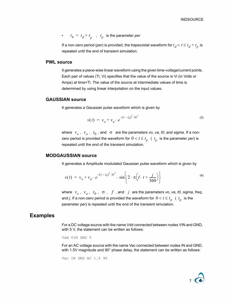
GAUSSIAN source
It generates a Gaussian pulse waveform which is given by
where , , , and are the parameters vo, va, t0, and sigma. If a non-
zero period is provided the waveform for ( is the parameter per) is
repeated until the end of the transient simulation.
MODGAUSSIAN source
It generates a Amplitude modulated Gaussian pulse waveform which is given by
where , , , , , and are the parameters vo, va, t0, sigma, freq,
and j. If a non-zero period is provided the waveform for ( is the
parameter per) is repeated until the end of the transient simulation.
Examples
For a DC voltage source with the name Vdd connected between nodes VIN and GND, with 5 V, the statement can be written as follows:
Vdd VIN GND 5
For an AC voltage source with the name Vac connected between nodes IN and GND, with 1.5V magnitude and 90° phase delay, the statement can be written as follows:
Vac IN GND AC 1.5 90
(3)
(4)
t4 td t+ p= tp
td t td tp+
v t vo va et t0– 2 2–
+=
vo va t0 0 t tp tp
v t vo va et t0– 2 2–
2 f t j360---------+
sin +=
vo va t0 f j0 t tp tp

INDSOURCE
8
For a current source with the name Isrc1 that generates a current flow from GND to IN with DC current = 1 mA, with AC magnitude = 1 mA and AC phase = 90°, and with sinusoidal transient function with amplitude = 1.5 mA and frequency = 1 GHz, the statement can be written as follows:
Isrc1 GND IN DC=1m AC=1m 90 SIN 0 1.5 1G 0
For a pulse voltage source with device name Vpulse connected between nodes IN2 and GND, with initial voltage = 0.1 V, pulsed voltage = 2 V, time delay = 2 ns, rise/fall time = 0.5 ns, pulse width = 1.2 ns, and period = 3 ns, the statement can be written as follows:
Vpulse IN2 GND PULSE 0.1 2 2n 0.5n 0.5n 1.2n 3n
For a PWL voltage source with device name Vpwl connected between nodes 1 and 2, with time voltage pair {0s, 0V}, {0.1ns, 1V}, {0.3ns, 2.5V}, {0.6ns, 2.5V}, {0.7ns, 1.8V}, and {1.0 ns, 0V}, the statement can be written as follows:
Vpwl 1 2 PWL 0.0 0.0 0.1n 1 0.3n 2.5 0.6n 2.5 0.7n 1.8 1n 0.0

DEPSOURCE
9
DEPSOURCE
Syntax
Style Form
SPICE Voltage Controlled Voltage Source (VCVS) - linear
Exxx n+ n- <VCVS> in+ in- gain <MAX=val> <MIN=val>
VCVS - polynomial
Exxx n+ n- <VCVS> POLY(NDIM) in1+ in1-... p0 p1 p2 ... <MAX=val> <MIN=val>
Current Controlled Current Source (CCCS) - linear
Fxxx n+ n- <CCCS> vsrc gain <MAX=val> <MIN=val>
CCCS - polynomial
Fxxx n+ n- <CCCS> POLY(NDIM) vsrc1 vsrc2 ... p0 p1 p2 ... <MAX=val> <MIN=val>
Voltage Controlled Current Source (VCCS) - linear
Gxxx n+ n- <VCCS> in+ in- transconductance <MAX=val> <MIN=val>
VCCS - polynomial
Gxxx n+ n- <VCCS> POLY(NDIM) in1+ in1-... p0 p1 p2 ... <MAX=val> <MIN=val>
Voltage Controlled Resistor (VCR) - linear
Gxxx n+ n- VCR in+ in- transfactor <MAX=val> <MIN=val>
VCR - polynomial
Gxxx n+ n- VCR POLY(NDIM) in1+ in1-... p0 p1 p2 ... <MAX=val> <MIN=val>
Current Controlled Voltage Source (CCVS) - linear
Hxxx n+ n- <CCVS> vsrc transresistance <MAX=val> <MIN=val>
CCVS - polynomial
Hxxx n+ n- <CCVS> POLY(NDIM) vsrc1 vsrc2 ... p0 p1 p2 ... <MAX=val> <MIN=val>

DEPSOURCE
10
Nodes
Electrical Positive node
Electrical Negative node
Control Nodes (CNodes)
Electrical Controlling positive and negative nodes
OptiSPICE Voltage dependent sources - linear
Osp DEPSOURCE Name=name EL_Type=TYPE Nodes=[ n+ n-] CNodes = [in+ in-]
+ Gain=val <MAX=val> <MIN=val>
Voltage dependent sources - polynomial
Osp DEPSOURCE Name=name EL_Type=TYPE Nodes=[ n+ n-]
+ CNodes = [in1+ in1- ...] Mode = POLY nPoly=NDIM Pcoeff = [ p0 p1 ...]
+ <MAX=val> <MIN=val>
Current dependent sources - linear
Osp DEPSOURCE Name=name EL_Type=TYPE Nodes=[ n+ n-] Ielems=vsrc
+ Gain=val <MAX=val> <MIN=val>
Current dependent sources - polynomial
Osp DEPSOURCE Name=name EL_Type=TYPE Nodes=[ n+ n-]
+ Ielems=[vsrc1 vsrc2 ...] Mode = POLY nPoly=NDIM Pcoeff = [ p0 p1 ...]
+ <MAX=val> <MIN=val>
Voltage source depndence expressed by equation
Osp DEPSOURCE Name=name Nodes=[ n+ n-] Mode = VOL EQ=’expr’
+ <MAX=val> <MIN=val>
Current dependence expressed by equation
Osp DEPSOURCE Name=name Nodes=[ n+ n-] Mode = CURR EQ=’expr’
+ <MAX=val> <MIN=val>
Name Signal Type Description
n+
n-
Name Signal Type Description
in1, in2, ....
Style Form

DEPSOURCE
11
Controlling Currents (Ielems)
Electrical Name of voltage sources through which controlling currents flow
Parameters
Dependant source type
Type of dependent source.
EL_Type VCVS - VCVS, CCCS, VCCS, CCVS, VCR
Control current elements
List of voltage source elements through which the control current flows.
Ielems - - -
Dependent source function mode
Function types to represent special behavior of the dependent source. VOL and CURR are used to mathematically express (as equations) voltage and current respectively as a function of node voltages and/or current through voltage sources.
Mode POLY - POLY, VOL, CURR
Polynomial dimension
Number of polynomial dimension
nPoly 1 - [0, +INF[
Polynomial coefficients
Polynomial coefficients to describe the polynomial function of controlled source
Pcoeff - - ]-INF, +INF[
Gain
Gain of dependent source in case of linear dependency
GAIN 1 - ]-INF, +INF[
Equation
Equation that models the behavior of the controlled source
EQ - - -
Maximum magnitude value
The maximum voltage, current or resistance of the dependent element
MAX 1e12 A, V or ohm ]-INF, +INF[
Minimum magnitude value
The minimum voltage, current or resistance of the dependent element
MIN -1e12 A, V or ohm ]-INF, +INF[
Name Signal Type Description
vsrc1, vscr2, ...
Name and description Symbol Default value Units Value range
DEPSOURCE
12
Technical Background
The DEPSOURCE are linear dependent (or controlled) sources. They are
characterized by linear relationships between voltage and current. If we use i to
represent the current and v to represent the voltage, the relationships can be defined
by , where G is the transconductance; , where E is the voltage gain;
, where F is the current gain; and , where H is the transresistance.
Examples
For a voltage controlled voltage source (VCVS) with the name E1 connected between nodes 1 and 2, controlled by voltage difference between IN1 and IN2 with a gain of 10 and maximum limit of 15 V, the statement can be written as follows:
E1 1 2 IN1 IN2 10 MAX=15
For a polynomial VCVS with the name Eply connected between nodes 3 and 4, and controlled by voltage differences between nodes {IN1, IN2} and {IN3,IN4} with polynomial coefficients p0 = 3, p1 = 0.8, p2 = 0.5, the statement can be written as follows:
Eply 3 4 POLY(2) IN1 IN2 IN3 IN4 3 0.8 0.5
For a current controlled current source (CCCS) with the name F1 connected between nodes n1 and n2, controlled by current through voltage source Vs with a gain of 25 and initial control current of 0.5 mA, the statement can be written as follows:
F1 n1 n2 Vs 25 IC=0.5m
For a polynomial (second order) CCCS with the name Fply connected between nodes 6 and ground, controlled by currents flowing through Vsrc1 and Vsrc2, with polynomial coefficients p0 = 2, p1 = 1.5, p2 = 0.8, p3 = 0.2, p4 = 0.1, p5 = 0.05, the statement can be written as follows:
Fply 6 0 POLY(2) Vsrc1 Vsrc2 2 1.5 0.8 0.2 0.1 0.05
For a voltage controlled current source (VCCS) with the name Gs connected between nodes 8 and 9, controlled by voltage difference between IN1 and IN2 with a transconductance of 1.5 and maximum limit of 10 mA, the first order temperature coefficient 0.5 mA/Deg.C and second order temperature coefficient 0.1 mA/Deg.C^2, the statement can be written as follows:
Gs 8 9 IN1 IN2 1.5 MAX=10m TC1=0.5m TC2=0.1m
For a voltage controlled resister (VCR) with device name Gres1 connected between nodes 11 and 12, controlled by voltage difference between IN1 and IN2 with a voltage-to resistance ratio of 1000, with minimum resistance 50 ohms, the statement can be written as follows:
Gres1 11 12 VCR IN1 IN2 1000 MIN=50
i Gv= v Ev=i Fi= v Hi=

DEPSOURCE
13
For a polynomial (second order) VCR with the name Gply connected between nodes 15 and 16, controlled by voltage differences between nodes IN1 and IN2 with polynomial coefficients p0 = 100, p1 = 10, and p2 = 5, and with a minimum resistance 1 ohm, he statement can be written as follows:
Gply SIG1 SIG2 VCR POLY(1) IN1 IN2 100 10 5 MIN=1
For a dependent current source, which is expressed as an equation, a sample netlist statement is given below:
Osp DEPSOURCE Name=Vdep1 Nodes=[ 3 0 ] Mode = CURR
+ Eq = '1e-12 * exp(40*(v(1) - v(2)))'

DEPSOURCE
14
Notes:

NOISESOURCE
15
NOISESOURCE
Syntax
Osp NOISESOURCE Nodes=[n1 n2] <param1=val1> <param2=val2> ....
Nodes
Electrical
Electrical
Parameters
Style Form
OptiSPICE
Name Signal Type Description
n1
n2
Name and description Symbol Default value Units Value range
Noise source type
Type of noise source (voltage or current)
Type I - I, V
Noise source mode
Frequency dependence mode of the noise source
Mode Res - Res, White, Pink
Noise distribution
Probability distribution functions to generate noise based on a Monte-Carlo method
Dist Gaussian - Gaussian, Poisson, WMC
Resistance
Resistance of the noise source
R 0 ohm [0, +INF[
Noise spectral density
Magnitude of noise spectral density
Magnitude 0 (V or A)^2/Hz [0, +INF[
Temperature
Noise source temperature
Temp 0 K ]-INF, +INF[
Pink noise calculation method
Method used to compute noise for frequency dependent Pink noise
Method Default - Default, Sequence,

NOISESOURCE
16
Technical Background
Noise source generates transient noise (current or voltage) between two nodes. A
noise value is generated at any given time point based on a Monte-Carlo method
using given noise spectral density and probability density function.
The parameter Mode sets the frequency dependence of the noise as given by
• Res - white noise resistor mode, noise spectral density = where K is
the Boltzmann constant, T is the temperature in Kelvin, and R is the resistance
• White - noise spectral density = given by parameter Magnitude
• Pink - noise spectral density = , where M is the parameter Magnitude, f
is a frequency value from the internally computed frequency spectrum, and AF is
the parameter AF.
Having the magnitude as the mean value, a probability density function is applied
such that the Monte-Carlo method will generate a noise value based on the probability
distribution: Gaussian, Poisson or WMC (given by Webb, Mclntyre, and Conradi [1] -
[3] for photodiode noise).
If the Method is set to Sequence, a sequence of noise is added at each time point.
The magnitude of the noise sequence is computed based on the frequency bandwidth
of the internal time step the simulator takes. If the Mode is set to Pink, then noise is
computed based on Sequence method such that a noise spectral density is computed
for a bandwidth which depends on the internal time step, and then it is converted to
time domain by applying inverse Fourier transform.
Examples
For a white noise source (current source) with the name WhiteNoiseSrc connected between NIN and ground with the noise density 1.5e-11 A^2/Hz, the statement can be written as follows:
Osp NOISESOURCE Name = WhiteNoiseSrc Type = I Nodes = [NIN 0]
+ Mode=White Magnitude = 1.5e-11
Flicker noise exponent
Flicker noise exponent used to compute a frequency dependent Flicker or Pink noise
AF 1.0 - ]-INF, +INF[
Name and description Symbol Default value Units Value range
4KT R
M fAF

NOISESOURCE
17
References
[1] P. P. Webb, R. J. McIntyre, and J. Conradi, “Properties of avalanche photo diodes,” RCA Rev., vol. 35, pp. 234-276, June 1974.
[2] Baker, K.R, "On the WMC density as an inverse Gaussian probability density", IEEE Trans. on Commun., Vol. 44, No. 1, 1996, pp. 15-17.
[3] Ascheid, G., "On the generation of WMC-distributed random numbers", IEEE Trans. on Commun., Vol. 38, No. 12, 1990, pp. 2117 - 2118.

NOISESOURCE
18
Notes:

OPTISYSINELEC
19
OPTISYSINELEC
Syntax
Nodes
Electrical Positive node
Electrical Negative node
Parameters
Signal file
Name of the text file that contain electrical signal data (generated by OptiSystem).
SignalFile - - -
Transient data input mode
Format for input signal data. For OptiSystem input only FILE mode is supported.
tranMode NONE - NONE, FILE
Element type
Defines the type of the element whether it is a current source (I_SOU) or a voltage source (V_SOU)
EL_Type 0.0 V I_SOU, V_SOU
Technical Background
The element OPTISYSINELEC is essentially an independent source (INDSOURCE)
that receives electrical input from OptiSystem during OptiSystem - OptiSPICE co-
simulation. The input electrical signal data file given by SignalFile contains two
columns: time and amplitude values. Depending on EL_Type it can act either as a
current or a voltage source.
Style Form
OptiSPICE Osp OPTISYSINELEC Name=devname Nodes=[n+ n-] SignalFile=filename
+ tranMode=FILE EL_Type=I_SOU/V_SOU
Name Signal Type Description
n+
n-
Name and description Symbol Default value Units Value range

OPTISYSINELEC
20
Notes:

RESISTOR
21
RESISTOR
Syntax
Osp RESISTOR Name = name <MoName = modelname> Nodes=[ n+ n- ] + <param1=val1> <param2=val2> ....
Nodes
Electrical Positive node
Electrical Negative node
Parameters
Style Form
SPICE Rxxx n+ n- <modelname> <R = >resistance <<TC1 = >val> <<TC2 = >val>
+ <SCALE = val> <M = val> <AC = val> <DTEMP=val> <L = val> <W = val> <C = val>
OptiSPICE
Name Signal Type Description
n+
n-
Name and description Symbol Default value Units Value range
Resistance
Resistance value
R 0 ohms [0, +INF[
AC resistance
Resistance for AC analysis
AC 0 ohms [0, +INF[
Scaling factor
Scaling factor for resistance value or resistor physical properties
SCALE 1 - [0, +INF[
Multiply factor
Parallel instances of this element
M 1 - [1, +INF[
Temperature Difference
The temperature difference between the element and the circuit
DTEMP 0 K ]-INF, +INF[
First order temperature coefficient
First order coefficient for the resistance calculation due to change in temperature
TC1 0 ohm/Deg. C ]-INF, +INF[

RESISTOR
22
Technical Background
A resistor is a two terminal electrical element that produces a voltage drop across its
terminals proportional to the current flowing through it as given by Ohm’s law
where is the resistance measured in Ohms, is the voltage drop across its
terminals in Volts, and is the current in Amperes.
Resistance as a function of temperature can be expressed as:
where : is the nominal temperature in Kelvin.
If noise simulation is performed and the parameter NoNoise is 0 (default choice), then
the noise spectral density of the current (unit A2/Hz) can be calculated as
Second order temperature coefficient
Second order coefficient for the resistance calculation due to change in temperature
TC2 0 ohm/ Deg. C^2 ]-INF, +INF[
Width
The physical width of the resistor wire model
W 1e-4 m [0, +INF[
Length
The physical length of the resistor for resistor wire model
L 1e-4 m [0, +INF[
Capacitance
Parasitic capacitance connected from node 2 to ground
C 0 F [0, +INF[
Exclude Noise
Exclude element noise (1) or not (0)
NoNoise 0 - 0, 1
(1)
(2)
(3)
Name and description Symbol Default value Units Value range
vR R iR=
R vRiR
R T R Tnom 1 TC1 DTEMP TC2 DTEMP2+ + =
Tnom
Ni4 K T R
-------------------=

RESISTOR
23
where is the Boltzmann constant
The resistance value can be specified as a value or an equation. A resistor model may
be provided to define physical characteristics of the wire model of a resistor. If
parameters C, W, L, TC1, and TC2 are provided in the element, they will replace
corresponding model parameters. For more details about resistor model see
Technical Background of resistor model.
Example
For a resistor with the name R1 connected between nodes 1 and 2 with 10 kilo-ohms,
and temperature coefficients (TC1 and TC2) of 0.01 and 0.001, the netlist statement
can be generated as follows:
R1 1 2 R=10k TC1=0.01 TC2=0.001
K

RESISTOR
24
Notes:

CAPACITOR
25
CAPACITOR
Syntax
Osp CAPACITOR Name = name <MoName = modelname> Nodes=[ n+ n- ] + <param1=val1> <param2=val2> ....
Nodes
Electrical Positive node
Electrical Negative node
Parameters
Style Form
SPICE Cxxx n+ n- <modelname> <C = >capacitance <<TC1 = >val> <<TC2 = >val>
+ <SCALE = val> <IC = val> <M = val> <W = val> <L = val> <DTEMP = val>
OptiSPICE
Name Signal Type Description
n+
n-
Name and description Symbol Default value Units Value range
Capacitance
Capacitance value
C 0 F [0, +INF[
Initial voltage
Initial voltage across the capacitor
IC 0 V ]-INF, +INF[
Temperature Difference
The temperature difference between the element and the circuit
DTEMP 0 K ]-INF, +INF[
First order temperature coefficient
First order coefficient for the capacitance calculation due to change in temperature
TC1 0 F/Deg. C ]-INF, +INF[
Second order temperature coefficient
Second order coefficient for the capacitance calculation due to change in temperature
TC2 0 F/ Deg. C^2 ]-INF, +INF[

CAPACITOR
26
Technical Background
This is a linear capacitor element which has two conductors separated by an insulator
to store electric charge when a voltage is applied across its conductors. Current
through the capacitor is given by
where is the capacitance measured in Farads, is the voltage drop across its
terminals in Volts, and is the time in seconds.
Capacitance as a function of temperature can be expressed as:
where : is the nominal temperature in Kelvin.
Capacitor model may be provided to define physical characteristics of a capacitor. For
more details about resistor model see Technical Background of capacitor model.
Example
For a capacitor with device name C1 connected between nodes 1 and 2 with 2 pF, and initial voltage of 0.05 V, the statement can be written as follows:
C1 1 2 C=2p IC=0.05
Scaling factor
Scaling factor for capacitance value or capacitor physical properties
SCALE 1 - [0, +INF[
Multiply factor
Parallel instances of this element
M 1 - [1, +INF[
Width
Width of the capacitor to replace physical capacitor model parameter
W 1e-4 m [0, +INF[
Length
Length of the capacitor to replace physical capacitor model parameter
L 1e-4 m [0, +INF[
(1)
(2)
Name and description Symbol Default value Units Value range
ic Cdvcdt--------=
C vct
C T C Tnom 1 TC1 DTEMP TC2 DTEMP2+ + =
Tnom

INDUCTOR
27
INDUCTOR
Syntax
Osp INDUCTOR Name = name Nodes=[ n+ n- ] <param1=val1> <param2=val2> ....
Nodes
Electrical Positive node.
Electrical Negative node.
Parameters
Style Form
SPICE Lxxx n+ n- <L = >inductance <IC = val> <DTEMP = val> <TC1 = val> <TC2 = val>
+ <SCALE = val> <M = val> <ExtTnode = nodename> <Rth = val> <Cth = val>
OptiSPICE
Name Signal Type Description
n+
n-
Name and description Symbol Default value Units Value range
Inductance
The inductance value of the inductor
L 1e-4 H [0, +INF[
Initial current
Initial current flowing through the inductor
IC 0 A ]-INF, +INF[
Temperature Difference
The temperature difference between the element and the circuit
DTEMP 0 K ]-INF, +INF[
First order temperature coefficient
First order coefficient for the inductance calculation due to change in temperature
TC1 0 H/Deg. C ]-INF, +INF[
Second order temperature coefficient
Second order coefficient for the inductance calculation due to change in temperature
TC2 0 H/ Deg. C^2 ]-INF, +INF[

INDUCTOR
28
Technical Background
The Inductor is a two terminal element that can store energy in magnetic field when a current is passing though. The voltage induced across the terminals of the inductor is given by
vL LdiLdt-------= (1)
where is the inductance measured in Henries, is the current through the
inductor in Amperes, and is the time in seconds.
Inductance as a function of temperature can be expressed as:
where : is the nominal temperature in Kelvin.
An optional, physical-based, Inductor model can also be used with the Inductor element. Please see the “Electrical Models” section (Inductor Model) for further details.
Example
For an inductor with the name L1 connected between nodes N1 and N2 with 10 nH, initial current = 0.01 mA, the statement can be written as follows:
L1 N1 N2 L=10n IC=0.01m
Scaling factor
Scaling factor for inductance value or inductor physical properties
SCALE 1 - [0, +INF[
Multiply factor
Parallel instances of this element
M 1 - [1, +INF[
(2)
Name and description Symbol Default value Units Value range
L iLt
L T L Tnom 1 TC1 DTEMP TC2 DTEMP2+ + =
Tnom

NRESISTOR
29
NRESISTOR
Syntax
Osp NRESISTOR Name=name Nodes=[n+ n-] <param1=val1> <param2=val2> ....
Nodes
Electrical Positive node
Electrical Negative node.
Parameters
Style Form
OptiSPICE
Name Signal Type Description
n+
n-
Name and description Symbol Default value Units Value range
Element type
Element’s current-voltage relationship expression type: RES - resistance, COND - conductance, CURR - current
Type RES - RES, COND, CURR
Function mode
Non-linear function mode: POLY - polynomial function of voltage; EQ - resistance function as a mathematical expression
Mode POLY ohm POLY, EQ
Polynomial coefficients
List of coefficients representing polynomial function from zeroth order to higher order
coeff - - ]-INF, +INF[
Equation
Equation expression
Eq - ohms -
Maximum voltage
Maximum voltage across the terminals for resistance calculation
Vmax 1e50 V ]-INF, +INF[
Minimum voltage
Minimum voltage across the terminals for resistance calculation
Vmin -1e50 V ]-INF, +INF[

NRESISTOR
30
Technical Background
The NResistor (non-linear resistor) can be used to express resistance as a non-linear
function of nodal voltages, branch currents, and time. This element can be expressed
either as a resistance function (voltage/current), conductance function
(current/voltage), or a function expressing current through resistor
(voltage/resistance) depending on the parameter Type values RES, COND, or CURR
respectively.
There are two function modes available: polynomial (POLY) and equation (EQ). If set
to POLY (default choice), then the function need to be expressed as a polynomial
function of voltage difference between nodes n+ and n- as follows.
where is the voltage difference between nodes n+ and n-,
are the polynomial coefficients given by the coeff parameter, and is the order of
polynomial.
Temperature polynomial coefficients
Temperature polynomial coefficients for the dependency of current on temperature
Tcoeff - - ]-INF, +INF[
Offset temperature
Offset value from the device temperature
Toff 0 K ]-INF, +INF[
Temperature difference
The temperature difference between the element and the circuit
DTEMP 0 K ]-INF, +INF[
Temperature node
The name of the external temperature node
ExtTNode - - -
Thermal resistance
Thermal resistance of element
Rth 0 K/W [0, +INF[
Thermal capacitance
Thermal capacitance of element
Cth 0 W sec/K [0, +INF[
(1)
Name and description Symbol Default value Units Value range
f v p0 p1v p2v2 pNv
N+ + + +=
v p0 p1 p2 pN N

NRESISTOR
31
If the Mode is EQ, then it can be expressed as a function of any nodal voltages,
currents through voltage sources, and time by defining a mathematical expression to
the Eq parameter.
Parameters Vmax and Vmin restrict the voltage across the n+ and n- not to go beyond
the limit for the resistance calculation.
Thermal Operation
Parameters Rth and Cth can be set to create a simple thermal sub-circuit for the
device. However, the parameter ExtTnode can be used to specify an external
temperature node to which an external thermal network can be attached.
The temperature dependence are specified by the polynomial list parameter
Tcoeff= , where is the order of the polynomial. The
current through the element as a function of temperature in Kelvin can be
expressed as:
where
• is the nominal temperature in Kelvin
•
• is the parameter Toff (offset temperature) in Kelvin
Example
For a polynomial non-linear resistor with the name NR1 connected between nodes 1
and ground with a polynomial coefficients p0 = 1000, p1 = -500, p2 = 3000, and p3 =
500, the statement can be written as follows:
Osp NResistor Name=NR1 Nodes=[1 0] coeff=[ 1000 -500 3000 500 ]
For a polynomial non-linear resistor that need to be expressed current function
with the name NCur1 connected between nodes
1 and 2, the statement can be written as follows:
Osp NResistor Name=NCur1 Nodes=[1 2] Type=CURR
+ coeff = [ 0.05 0.01 0.001]
(2)
pT0 pT1 pT2 pTM MT
i T i Tnom pT0 pT1Td pT2Td2 pTMTd
M+ + + + =
Tnom
Td T Toff–=
Toff
i 0.05 0.01 v 0.001 v2++=

NRESISTOR
32
For a non-linear resistor with name R1 connected between node 1 and 2, and its value
expressed mathematically as where
, the statement can be expressed as:
Osp NResistor Name=R1 Nodes=[1 2] Mode = EQ
+ Eq = ‘50 + 10 * V(in1,in2) * exp(1.5e9*TIME)’
R 50 10+ vin1 vin2– e kt– =k 1.5 10
9=

NCAPACITOR
33
NCAPACITOR
Syntax
Nodes
Electrical Positive node.
Electrical Negative node
Parameters
Capacitor type
To define capacitor as a charge function (QDEF) or capacitance function (CDEF)
Type QDEF - QDEF, CDEF
Zeroth order polynomial coefficient
Zeroth order polynomial coefficient value for the capacitance function represented as a polynomial function of voltage
D 0 - ]-INF, +INF[
First order polynomial coefficient
First order polynomial coefficient value for the capacitance function represented as a polynomial function of voltage
C 0 - ]-INF, +INF[
Second order polynomial coefficient
Second order polynomial coefficient value for the capacitance function represented as a polynomial function of voltage
B 0 - ]-INF, +INF[
Third order polynomial coefficient
Third order polynomial coefficient value for the capacitance function represented as a polynomial function of voltage
A 0 - ]-INF, +INF[
Style Form
OptiSPICE Osp NCAPACITOR Name=name Nodes=[n+ n-] <param1=val1> <param2=val2> ....
Name Signal Type Description
n+
n-
Name and description Symbol Default value Units Value range

NCAPACITOR
34
Technical Background
The NCapacitor (non-linear capacitor) can be used to express capacitance as a
polynomial function of voltage across its terminals. If the parameter Type is defined
as QDEF (default choice), the non-linear charge (Q) stored in the capacitor, is
expressed as a function of v (voltage difference between node n+ and n-) as given by:
where A, B, C, and D are the element parameters representing third, second, first, and
zeroth order polynomial coefficients respectively.
If Type is set to CDEF, then capacitance (C) is expressed as a function of voltage
across n+ and n- as follows
Examples
For a non-linear capacitor to be expressed as a nonlinear charge with the name NC1,
connected between nodes 1 and ground with polynomial coefficients A = 1e-9, B =
1.5e-8, C=2e-7, and D = 1e-7, the netlist statement can be written as:
Osp NCapacitor Name=NC1 Nodes=[1 0] A=1e-9 B=1.5e-8 C=2e-7 D=1e-7
For a non-linear capacitor to be expressed as a nonlinear capacitance with the name
NC2, connected between nodes 2 and ground with polynomial coefficients (for
charge) B = 3e-11, C=2.5e-10, and D = 1e-12, the netlist statement can be written as:
Osp NCapacitor Name=NC2 Nodes=[2 0] Type=CDEF B=3e-11 C=2.5e-10
+ D=1e-12
(1)
(2)
Q v Av3Bv
2Cv D+ + +=
C v Av3Bv
2Cv D+ + +=

MUTUALIND
35
MUTUALIND
Syntax
Parameters
Inductors
Names of coupling inductors
Inductors - - -
Coupling coefficient
Coefficient for coupling between the two inductors
K 0 - [0, 1]
Technical Background
The MUTUALIND is a mutual or coupled inductor that represents coupling between
two inductors. The mutual inductance, , is defined by
where
• is the coupling coefficient
• is the inductance of first inductor in Henries
• is the inductance of second inductor in Henries
Example
For a mutual inductor K1 forming coupling between two inductors L1 and L2 with coupling coefficient = 0.75, the statement can be written as follows:
K1 L1 L2 K=0.75
Style Form
SPICE Kxxx Lyyy Lzzz <K = >couplingcoeff
OptiSPICE Osp MUTUALIND Name = name Inductors = [ind1_name ind2_name] K=val
Name and description Symbol Default value Units Value range
(1)
M
M k L1L2=
k
L1
L2

MUTUALIND
36
Notes:
TRANLINE
37
TRANLINE
Syntax
Nodes
Electrical
Electrical
Parameters
Length of conductor
The length of the conductors
L 1e-4 m [0, +INF[
Number of lump segments
The number of sections (lumps) in a transmission line model that representing a small length (small fraction of a wavelength) of the transmission line operating at the highest frequency
LUMPS 20 - [0, +INF[
Technical Background
Transmission line characteristics are in general described by Telegrapher’s
equations.
Transmission line element is represented as lumped elements having series
resistance and inductance, and shunt conductance and capacitance (RLGC). Per-
Style Form
SPICE UXXX IN1 IN2 ... INN INREF OUT1 OUT2 ... OUTN OUTREF modelname <L=val>
+ <LUMPS=val> ....
OptiSPICE Osp TRANLINE Name = name Mode = U
+ Nodes = [N1 IN2 ... INN INREF OUT1 OUT2 ... OUTN OUTREF]
+ Model = modelname <L=val> <LUMPS=val>
Name Signal Type Description
n1
n2
Name and description Symbol Default value Units Value range

TRANLINE
38
unit-length (p.u.l) RLGC parameters are given using Transmission line model (U). For
more details see Technical Background of Lumped Transmission Line (U) Model.
Example
For two conductor lumped transmission lines with device name U2 connected to
nodes IN1, IN2, OUT1, and OUT2 (ground input and output references) with a length
of 12 cm and 60 lumped segments, and represented by the model name
LUMPMODEL, the statement can be written as follows:
U2 I1 I2 GND O1 O2 GND LUMPMODEL L=0.12 LUMPS=60

IDEALTRANLINE
39
IDEALTRANLINE
Syntax
Nodes
Electrical Input node
Electrical Input reference node
Electrical Output node
Electrical Output reference node
Parameters
Characteristic impedance
Characteristic impedance of the line
Z0 50 Ohm [0, +INF[
Time delay
Propagation delay of the line
TD 0 sec [0, +INF[
Technical Background
Ideal transmission line is a single conductor transmission line without loss and it is
characterized by propagation delay and characteristic impedance. Equivalent circuit
is given by Figure 1.
Style Form
SPICE TXXX In RefIn Out RefOut Z0 TD
OptiSPICE Osp IDEALTRANLINE Name = name Nodes = [In RefIn Out RefOut] <Z0=val>
+ <TD=val>
Name Signal Type Description
In
Refin
Out
RefOut
Name and description Symbol Default value Units Value range

IDEALTRANLINE
40
Figure 1 Equivalent circuit for ideal transmission line
The equations representing this element can be given by.
where
• , , , and are nodes In, RefIn, Out, and RefOut respectively
•
•
Example
For an ideal transmission line with the name T1, connected to node In1, GND, Out1, and GND with characteristic impedance = 100 Ohms and line delay = 2 ns, the statement can be written as follows:
T1 In1 GND Out1 GND 100 2n
(1)
v1 t vn3 n4 t TD– Z0 i2 t TD– +=
v2 t vn1 n2 t TD– Z0 i1 t TD– +=
n1 n2 n3 n4
vn1 n2 t vn1 t vn2 t –=
vn3 n4 t vn3 t vn4 t –=

DELAY
41
DELAY
Syntax
Nodes
Electrical
Electrical
Parameters
Gain
Gain of the delay element
A (Gain ,Atten) 1.0 - ]-INF, +INF[
Delay
Delay time
Del 1.0 sec [0, +INF[
Technical Background
For a input voltage the delay element produces an output voltage of
where is the parameter A and is the parameter Del.
Example
For a delay element with the name Delay1, connected to node Din and Dout having a delay of 10 ns and a gain of 0.75, the statement can be written as follows:
Osp DELAY Name = Delay1 Nodes= [Din Dout] Del = 10n A = 0.75
Style Form
OptiSPICE Osp DELAY Name=name Nodes=[n1 n2] <param1=val1> <param2=val2> ....
Name Signal Type Description
n1
n2
Name and description Symbol Default value Units Value range
v t A v t – A

DELAY
42
Notes:

SPARAM
43
SPARAM
Syntax
Nodes
Electrical Ports 1 to N
Vref node
Electrical Reference node
Parameters
Style Form
OptiSPICE Osp SPARAM Name=name Nodes=[1 2 3 ... N] Vref = Ref <param1=val1>
+ <param2=val2> ....
Name Signal Type Description
1, 2, 3, ..., N
Name Signal Type Description
Ref
Name and description Symbol Default value Units Value range
Touchstone file
Name of the Touchstone file that contain the measured S-parameter data
tstonefile - - -
Number of poles
The total number of poles for the S-parameter element
NPoles 10 - [0, +INF[
Real poles
Option to specify whether all poles must be real (1) or not (0)
RealPoles 0 - 0, 1
Poles in log scale
Option to specify whether poles are represented in logarithmic scale (1) or not (0)
PolesLogScale 0 - 0, 1

SPARAM
44
Technical Background
This element is a multi-port linear network element that allows users to define S-
(Scattering) parameter data through following two ways:
• Touchstone file - S-parameter measurement data file
• Pole-residue file - created with OptiSPICE Filter Parameter Extractor.
Touchstone file is an de facto industry-standard file format for providing S-parameter
measurement data. The file name is given by the parameter tsonefile. If this file is
given a Vector Fitting algorithm [1] is internally used to generate poles and residues
for the linear network element. Number of poles are specified by the parameter
NPoles. If the parameter RealPoles is set to 1 all the poles generated by the fitting
algorithm will be real. However, this type of fitting will be suitable if the measured data
is smooth (no oscillations).
Instead of providing Touchstone file directly to the netlist, the Touchstone file can be
given as an input for the OptiSPICE Filter Parameter Extractor tool in order to obtain
pole-residue data output file, which is given by the parameter rfmfile. Filter Parameter
Extractor tool provides in interactive user interface to change number of poles and
view the fitting results in order to ensure accuracy of fitting. For more details see
OptiSPICE Filter Parameter Extractor documentation.
Example
For a two port S-parameter with device name S1 connected to nodes P1 and P2 with reference node Ref, and represented by pole-residue file having a file path C:\Filter\Bessel.prf, the statement can be written as follows:
Osp SPARAM Name=S1 Nodes=[ P1 P2 ] Vref=Ref
+ rfmfile="C:\Filter\Bessel.prf"
For a four port S-parameter represented with Touchstone file (filter.s4p) with device name S2 connected to nodes 1, 2, 3, and 4 with ground reference, and number of poles to be generated are 25, the statement can be written as follows:
Osp SPARAM Name=S2 Nodes=[1 2 3 4] tstonefile = filter.s4p Npoles = 25
Pole-residue file
File generated by OptiSPICE Filter Parameter Extractor containing the poles and residues that describes the filter
rfmfile - - -
Name and description Symbol Default value Units Value range

SPARAM
45
Reference
[1] B. Gustavsen and A. Semlyen, “Rational approximation of frequency domain responses by Vector Fitting", IEEE Trans. Power Delivery, vol. 14, no. 3, pp. 1052- 1061, July 1999.

SPARAM
46
Notes:

DIODE
47
DIODE
Syntax
Osp DIODE Nodes=[n+ n-] <param1=val1> <param2=val2> ....
Nodes
Electrical Positive node.
Electrical Negative node.
Parameters
Style Form
SPICE Dxxx n1 n2 modelname <<AREA = >area> <<PJ = >val> <IC = vd> <M = val>
+ <RS=val> <NoNoise=0/1> <DTEMP = val> <ExtTnode=nodename> <Rth=val>
+ <Cth=val>
OptiSPICE
Name Signal Type Description
n1
n2
Name and description Symbol Default value Units Value range
Junction area
PN junction area of the Diode
AREA 1 m^2 [0, +INF[
Junction periphery
Periphery of the PN junction of the diode
PJ 0 m^2 [0, +INF[
Initial condition
Initial voltage across the diode
IC 0 V ]-INF, +INF[
Multiply factor
Multiplying Factors refers to the number of the same elements connected in parallel
M 1 - [1, +INF[
Diode series resistance
Series resistance associated with the diode
RS 0 Ohm [0, +INF[
Exclude noise
Exclude element noise (1) or not (0)
NoNoise 0 - 0, 1

DIODE
48
Technical Background
A diode is an active electrical element that is formed by regions of p and n-type
semiconducting materials and exhibits non-linear voltage(V)-current(I) characteristics
in a circuit network. For supported model details see Technical Background of Diode
Model.
Example
For a diode with the name Dx connected between nodes 1 and 2 with a model name DMOD and initial voltage = 0.23V, the statement can be written as follows:
Dx 1 2 DMOD IC=0.23
Temperature difference
The temperature difference between the element and the circuit
DTEMP 0 K ]-INF, +INF[
Temperature node
The name of the external temperature node
ExtTNode - - -
Thermal resistance
Thermal resistance of element
Rth 0 K/W [0, +INF[
Thermal capacitance
Thermal capacitance of element
Cth 0 W sec/K [0, +INF[
Name and description Symbol Default value Units Value range

BITGEN
49
BITGEN
Syntax
Nodes
Electrical First port.
Electrical Second port.
Parameters
Style Form
OptiSPICE Osp BITGEN Name=name Nodes=[n1 n2] <param1=val1> <param2=val2> ....
Name Signal Type Description
n1
n2
Name and description Symbol Default value Units Value range
Line code
Binary code used to represent the voltage waveform
LineCode NRZ - NRZ, RZ
Rectange shape
Determines the shape for the edges of the pulse: EXP - exponential; LIN - linear
PuseShape EXP - EXP, LIN
Bit amplitude
Peak-to-peak amplitude of the pulse
BitMag 1 V ]-INF, +INF[
Bias
DC offset of the pulse
DCOffSet 0 V ]-INF, +INF[
Bit length
Length of time that constitutes a bit
Length 1e-8 sec [0, +INF[
Rise time
Defined as the time from when the rising edge reaches 10% of the amplitude to the time it reaches 90% of the amplitude
RiseTime 0 sec [0, +INF[
Fall time
Defined as the time from when the falling edge reaches 90% of the amplitude to the time it reaches 10% of the amplitude
FallTime 0 sec [0, +INF[

BITGEN
50
Technical Background
The BitGen element is a voltage source that generates voltage pulses for an internally
generated pseudorandom bit sequence or for a user given bit stream. It generates a
Non Return to Zero (NRZ) or Return to Zero (RZ) coded signal depending on the
LineCode parameter.
The high and low logic voltage levels are determined by the parameters BitMag and
DCOffset such that magnitude of logic 1 will be at BitMag + DCOffset while logic 0 will
be at DCOffset.
By default, with no user defined bit stream, pseudorandom bits are generated until the
end of simulation time. If a specific bit stream is given using BitStream parameter, the
bit stream can be repeated as a cycle for a given number of bits, given by parameter
Period. If Period is -1, then only one cycle is generated. If number of bits in period are
greater than the number of bits in Bitstream, then rest of the bits are filled with 0s,
otherwise, number of bits in Bitstream are capped by number of bits in Period.
The parameter PulseShape determines the shape for the edges of the pulse during
rise and fall transitions.
Duty cycle for RZ pulse
Ratio (in percentage) of the pulse duration with respect to bit length. The pulse duration defined to be the time interval between 50% of the peak amplitude points.
DutyCycle 50 % [0, 100]
Bit stream
User defined bit sequence. If not given, random bits will be generated
BitStream - - -
Number of bits in one period
Number of bits to be repeated as a cycle when bit stream is given. If Period is -1 (default) then only one cycle of bits in the Bitstream are generated. If number of bits in period are greater than the number of bits in Bitstream, then rest of the bits are filled with 0s, otherwise, number of bits in Bitstream are capped by number of bits in Period.
Period -1 - [0, +INF[
Name and description Symbol Default value Units Value range

BITGEN
51
NRZ Pulse
In case of an NRZ pulse the the waveform changes only during transitions: 0 to 1,
rising transition, and 1 to 0, falling transition. In other times the waveform remain
unchanged.
If the PulseShape is set to EXP (exponential), waveforms (normalized to the peak-to
peak pulse amplitude) for the rising and falling transitions are given by
where
• and
•
• and are the parameters RiseTime and FallTime respectively
If PulseShape is set to LIN (linear), the waveforms for rising and falling transitions are
given by
where and .
RZ Pulse
Unlike the NRZ pulse, for each 1-bit, the waveform rise to the high value and
immediately fall towards the low value during the bit period (by parameter
Length).
(1)
(2)
vr t 1 et tr 2–
–=
vf t et tf 2–
=
tr Tr K= tf Tf K=
K 0.1 ln– 0.9 ln––=
Tr Tf
vr t t trL=
vf t 1 t tfL–=
trL Tr 0.8= tfL Tf 0.8=
VHVL T

BITGEN
52
If the PulseShape is set to EXP, waveform for logic 1 normalized to the peak-to-peak
pulse amplitude is given by
where
•
•
If PulseShape is set to LIN, normalized pulse waveform for logic 1 is given by
where
•
•
•
Example
For a bit generator with name B1 generating NRZ coded random bits with a magnitude of 1 V, bit length of 0.1 ns, and rise and fall time of 0.01 ns, the netlist statement can be written as follows:
Osp BITGEN Name=B1 Nodes=[In 0] BigMag=1 Length=0.1n
+ RiseTime=0.01ns FallTime=0.01ns
For a bit generator with the name B2 generating RZ coded random bits with linear pulse shape, and with a magnitude of 5 V, bit length of 0.25 ns, rise time of 0.05 ns, fall time of 0.07 ns, and 40% duty cycle, the netlist statement can be written as follows:
Osp BITGEN Name=B2 Nodes=[In2 0] LineCode=RZ PulseShape=LIN
+ BigMag=5 Length=0.25n RiseTime=0.05ns FallTime=0.07ns
+ DutyCycle=40
(3)
(4)
v t 1 e
t tr 2–– 0 t t ,
e
t t–tf
------------
2
–
t t T,
=
t 2 ln tr tf– tpulse+=
tpulse T DutyCycle 100=
v t
t trL 0 t t1,
1 t1 t t2
1 t t2– tfL– t2 t t3,
0 t3 t T
=
t1 trL=
t2 0.5 trL tfL– tpulse+=
t3 t2 t+ fL=

BITGEN
53
For a BitGen element with the name B3 with a bit stream of 011010, bit magnitude of 2.5 V, bit length of 10ns, rise and fall time of 2 ns, , and the bit stream cycle to be repeated for every six bits, the statement can be written as follows:
Osp BITGEN Name=B3 Nodes=[In3 0] BitStream = 011010
+ BitMag=2.5 Length=10n RiseTime=2n FallTime=2n Period=6

BITGEN
54

NONLINVI
55
NONLINVI
Syntax
Nodes
Electrical
Electrical
Parameters
Style Form
OptiSPICE Osp NONLINVI Name=name Nodes=[n1 n2] <param1=val1> <param2=val2> ....
Name Signal Type Description
n1
n2
Name and description Symbol Default value Units Value range
Coefficients
Polynomial coefficients
coeff - - ]-INF, +INF[
Maximum current
The maximum current that the non-linear voltage current element can endure
Imax 1e50 A ]-INF, +INF[
Minimum current
The minimum current that the non-linear voltage current element can endure
Imin -1e50 A ]-INF, +INF[
Temperature polynomial coefficients
Temperature polynomial coefficients for the dependency of current on temperature
Tcoeff - K ]-INF, +INF[
Offset temperature
Offset value from the device temperature
Toff 0 K ]-INF, +INF[
Temperature difference
The temperature difference between the element and the circuit
DTEMP 0 K ]-INF, +INF[
NONLINVI
56
Technical Background
The NONLINVI can be used to express current as a polynomial function of nodal
voltages. The current, , can be expressed as a polynomial function of voltage, ,
difference between nodes n+ and n- as follows.
where are the polynomial coefficients given by the coeff
parameter, and is the order of polynomial.
Thermal Operation
Parameters Rth and Cth can be set to create a simple thermal sub-circuit for the
device. However, the parameter ExtTnode can be used to specify an external
temperature node to which an external thermal network can be attached.
The temperature dependence are specified by the polynomial list parameter
Tcoeff= , where is the order of the polynomial. The
current through the element as a function of temperature in Kelvin can be
expressed as:
where
• is the nominal temperature in Kelvin
•
• is the parameter Toff (offset temperature) in Kelvin
Temperature node
The name of the external temperature node
ExtTNode - - -
Thermal resistance
Thermal resistance of element
Rth 0 K/W [0, +INF[
Thermal capacitance
Thermal capacitance of element
Cth 0 W sec/K [0, +INF[
(1)
(2)
Name and description Symbol Default value Units Value range
i v
i p0 p1v p2v2 pNv
N+ + + +=
p0 p1 p2 pN N
pT0 pT1 pT2 pTM MT
i T i Tnom pT0 pT1Td pT2Td2 pTMTd
M+ + + + =
Tnom
Td T Toff–=
Toff

NONLINVI
57
Example
For a non-linear current element whose current voltage relationship is expressed as
, with maximum current of 250 mA and
minimum current of -250 mA, the statement can be written as follows:
Osp NonLinVI Name=VI1 Nodes = [1 2] coeff = [ -0.001 0.02 0.025 ]
+ Imax = 250mA Imin = -250mA
i 0.001– 0.02 v 0.025 v2++=

NONLINVI
58
Notes:

MOSFET
59
MOSFET
Syntax
Nodes
Electrical Drain terminal node
Electrical Gate terminal node
Electrical Source terminal node
Electrical Bulk/body terminal node (optional)
Parameters
Style Form
SPICE Mxxx nd ng ns <nb> modelname <<L = >length> <<W = >width> <AD = val>
+ <AS = val> <PD = val> <PS = val> <NRD = val> <NRS = val> <RDC = val>
+ <RSC = val> <OFF> <<IC = vdsval,vgsval,vbsval> or <VdsIC=val> <VgsIC=val>
+ <VbsIC=val>> <DELVTO = val> <GEO = val> <M = val> <NoNoise=0/1>
+ <DTEMP = val> <ExtTnode=nodename> <Rth=val> <Cth=val>
OptiSPICE Osp MOSFET Name = name MoName = modelname Nodes=[nd ng ns <nb>]
+ <param1=val1> <param2=val2> ....
Name Signal Type Description
nd
ng
ns
nb
Name and description Symbol Default value Units Value range
Channel length
Channel length of the MOSFET
L 1e-4 m [0, +INF[
Channel width
Channel width of the MOSFET
W 1e-4 m [0, +INF[
Drain diffusion area
Diffusion area of the drain terminal of the MOSFET
AD 0 m^2 [0, +INF[
Source diffusion area
Source terminal diffusion area of the MOSFET
AS 0 m^2 [0, +INF[
MOSFET
60
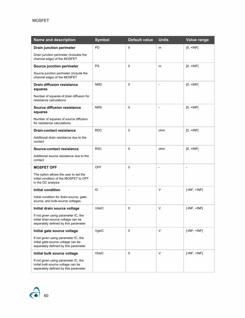
Drain junction perimeter
Drain junction perimeter (includes the channel edge) of the MOSFET
PD 0 m [0, +INF[
Source junction perimeter
Source junction perimeter (include the channel edge) of the MOSFET
PS 0 m [0, +INF[
Drain diffusion resistance squares
Number of squares of drain diffusion for resistance calculations
NRD 0 - [0, +INF[
Source diffusion resistance squares
Number of squares of source diffusion for resistance calculations.
NRS 0 - [0, +INF[
Drain-contact resistance
Additional drain resistance due to the contact
RDC 0 ohm [0, +INF[
Source-contact resistance
Additional source resistance due to the contact
RSC 0 ohm [0, +INF[
MOSFET OFF
The option allows the user to set the initial condition of the MOSFET to OFF in the DC analysis
OFF 0 - -
Initial condition
Initial condition for drain-source, gate-source, and bulk-source voltages.
IC - V ]-INF, +INF[
Initial drain source voltage
If not given using parameter IC, the initial drian-source voltage can be separately defined by this parameter
VdsIC 0 V ]-INF, +INF[
Initial gate source voltage
If not given using parameter IC, the initial gate-source voltage can be separately defined by this parameter
VgsIC 0 V ]-INF, +INF[
Initial bulk source voltage
If not given using parameter IC, the initial bulk-source voltage can be separately defined by this parameter
VbsIC 0 V ]-INF, +INF[
Name and description Symbol Default value Units Value range

MOSFET
61
Technical Background
The MOSFET is a four terminal electrical element that called metal oxide field-effect
transistor that is based on the modulation of charge concentration by a metal oxide
silicon capacitance between a body electrode and a gate electrode located above the
body and insulated from all other element regions by a gate dielectric layer which in
the case of a MOSFET is an oxide. Two additional terminals (source and drain), each
connected to individual highly doped regions that are separated by the body region.
These regions can be either p or n type, but they must both be of the same type, and
of opposite type of the body region. Using the gate contact on the oxide, the
operations of the MOSFET can be modified to the desired function. This transistor is
widely used in digital logic and analogue design. For supported models see Technical
Background of MOSFET Model.
Zero bias threshold voltage variation
Threshold voltage variation when the bias voltage is zero
DELVTO 0 V ]-INF, +INF[
Share source/drain selector
The option allows the user to define wether the drain or source alone is connected to another device or both are being connected to the one device
GEO 0 - [0, +INF[
Define Element Multiply Factor
Multiplying Factors refers to the number of the same elements connected in parallel
M 1 - [1, +INF[
Exclude Noise
Exclude element noise (1) or not (0)
NoNoise 0 - 0, 1
Temperature difference
The temperature difference between the element and the circuit
DTEMP 0 K ]-INF, +INF[
Temperature node
The name of the external temperature node
ExtTNode - - -
Thermal resistance
Thermal resistance of element
Rth 0 K/W [0, +INF[
Thermal capacitance
Thermal capacitance of element
Cth 0 W sec/K [0, +INF[
Name and description Symbol Default value Units Value range

MOSFET
62
Example
For a n-channel MOSFET with a device name M1 connected to nodes VDD, VI, VSS, and GND, with model name MNMOS, channel width = 2 µm, and channel length = 0.13 µm, the statement can be written as follows:
M1 VDD VI VSS GND MNMOS W=2u L=0.13u
BJT
63
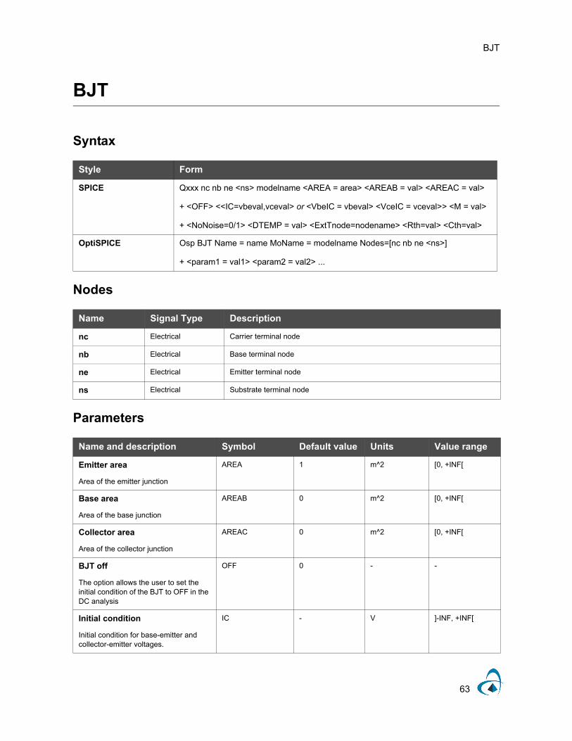
BJT
Syntax
Nodes
Electrical Carrier terminal node
Electrical Base terminal node
Electrical Emitter terminal node
Electrical Substrate terminal node
Parameters
Style Form
SPICE Qxxx nc nb ne <ns> modelname <AREA = area> <AREAB = val> <AREAC = val>
+ <OFF> <<IC=vbeval,vceval> or <VbeIC = vbeval> <VceIC = vceval>> <M = val>
+ <NoNoise=0/1> <DTEMP = val> <ExtTnode=nodename> <Rth=val> <Cth=val>
OptiSPICE Osp BJT Name = name MoName = modelname Nodes=[nc nb ne <ns>]
+ <param1 = val1> <param2 = val2> ...
Name Signal Type Description
nc
nb
ne
ns
Name and description Symbol Default value Units Value range
Emitter area
Area of the emitter junction
AREA 1 m^2 [0, +INF[
Base area
Area of the base junction
AREAB 0 m^2 [0, +INF[
Collector area
Area of the collector junction
AREAC 0 m^2 [0, +INF[
BJT off
The option allows the user to set the initial condition of the BJT to OFF in the DC analysis
OFF 0 - -
Initial condition
Initial condition for base-emitter and collector-emitter voltages.
IC - V ]-INF, +INF[

BJT
64
Technical Background
The BJT is called a bipolar junction transistor. It contains three different semiconductor doped regions with doping types of npn or pnp with three different corresponding region contacts (collector, base and emitter) that generate two diode (PN junctions) like structures that share a connection. The operation of the transistor depends on the bias condition on each of the two junctions. For details on supported BJT model types see Technical Background of BJT Model.
Example 1
For an NPN transistor with the name Q1 connected to nodes C, B, and E with model name NPNMOD, area factors of 1.2, 2.1, and 2.8 (for emitter, base, and collector respectively), and initial voltages VBE = 0.4 V, and VCE = 5 V, the statement can be written as follows:
Q1 C B E NPNMOD AREA=1.2 AREAB=2.1 AREAC=2.8 IC=0.4, 5
Initial base-emitter voltage
If not given using parameter IC, the initial base-emitter voltage can be separately defined by this parameter
VbeIC 0 V ]-INF, +INF[
Initial collector-emitter voltage
If not given using parameter IC, the initial collector-emitter voltage can be separately defined by this parameter
VceIC 0 V ]-INF, +INF[
Multiply factor
Multiplying Factors refers to the number of the same elements connected in parallel
M 1 - [1, +INF[
Exclude noise
Exclude element noise (1) or not (0)
NoNoise 0 - 0, 1
Temperature difference
The temperature difference between the element and the circuit
DTEMP 0 K ]-INF, +INF[
Temperature node
The name of the external temperature node
ExtTNode - - -
Thermal resistance
Thermal resistance of element
Rth 0 K/W [0, +INF[
Thermal capacitance
Thermal capacitance of element
Cth 0 W sec/K [0, +INF[
Name and description Symbol Default value Units Value range

BJT
65
Example 2 (Mextram)
For an NPN transistor with the name Q1 connected to nodes C, B, and E utilizing a Mextram level 504 model (with model name “mextram”), the statement can be written as follows:
Q1 C B E mextram
.model mextram NPN level = 504
Example 3 (Agilent)
For an PNP transistor with the name Q3 connected to nodes C, B, and E utilizing an Agilent model (with model name “agilent”), the statement can be written as follows:
Q3 C B E agilent
.model agilent PNP level = 101

BJT
66
Notes:

SWITCH
67
SWITCH
Syntax
Nodes
Electrical Positive node
Electrical Negative node
Parameters
Style Form
OptiSPICE Voltage controlled switch
Osp SWITCH Name=name Nodes=[n1 n2] CNodes=[in1 in2] <VON=val>
+ <VOFF=val> <RON=val> <ROFF=val>
Current controlled switch
Osp SWITCH Name=name Nodes=[n1 n2] VSRC=name <ION=val> <IOFF=val>
+ <RON=val> <ROFF=val>
Name Signal Type Description
n1
n2
Name and description Symbol Default value Units Value range
Switch type
Option to specify the type of the switch: voltage controlled (VCSW) or current controlled (CCSW)
SWTYPE VCSW - VCSW, CCSW
ON control voltage
Control voltage to be applied in order to change the resistance value to RON
VON 1.0 V ]-INF, +INF[
OFF control voltage
Control voltage to be applied in order to change the resistance value to ROFF
VOFF 0.0 V ]-INF, +INF[
ON control current
Control current to be applied in order to change the resistance value to RON
ION 1e-3 A ]-INF, +INF[

SWITCH
68
Technical Background
The switch element is a voltage or current controlled resistor having two different
resistance values RON and ROFF when turned on and off externally controlled by a
voltage or current.
For a voltage controlled switch, if VOFF < VON, the resistance, R, as a function of
controlling voltage, Vc, can be given as follows:
• For Vc VOFF, R = ROFF
• For Vc VON, R = RON
• For VOFF < Vc < VON, R can be expressed as
where
•
•
•
•
If VOFF > VON, then R = RON for Vc VON and R = ROFF for Vc VOFF. For
VOFF < Vc < VON, the relationship above equation will still hold.
OFF control current
Control current to be applied in order to change the resistance value to ROFF
IOFF 0.0 A ]-INF, +INF[
Controlling voltage source name
Name of the voltage source through which the control current flows
VSRC - - -
ON resistance
Resistance value when the switch is ON
RON 1.0 Ohm [0+, +INF[
OFF resistance
Resistance value when the switch is OFF
ROFF 1e6 Ohm [0+, +INF[
(1)
Name and description Symbol Default value Units Value range
R Lm 3 Lr Vx2 Vd
------------------------ 2 Lr Vx3
2 Vd3
---------------------------–+
exp=
Lm RON ROFF ln=
Lr RON ROFF ln=
Vx Vc VON VOFF+ 2–=
Vd VON VOFF–=

SWITCH
69
Current controlled switch has similar form where one needs to replace VON and
VOFF by ION and IOFF respectively for a controlling current Ic.
Examples
For a voltage controlled switch with the name SW1 connected to nodes 1 and 2, controlled by voltage difference between nodes 4 and 5, and having VON=2V, VOFF=1.5V, RON=0.1 Ohm, ROFF=5 Mega Ohm, the statement can be generated as follows:
Osp Switch Name=SW1 Nodes=[1 2] CNodes=[4 5]
+ VON=2 VOFF=1.5 RON=0.1 ROFF=5MEG
For a current controlled switch with the name SW2 connected to nodes A and B, controlled by a current through a voltage source name V1, and having ION=10mA, IOFF=2mA, RON=0.5 Ohm, ROFF=2 Mega Ohm, the statement can be generated as follows:
Osp Switch Name=SW2 SWTYPE=CCSW Nodes=[A B] VSRC=V1
+ ION=10m IOFF=2m RON=0.5 ROFF=2MEG

SWITCH
70
Notes:

JFET
71
JFET
Syntax
Nodes
Electrical Drain terminal node
Electrical Gate terminal node
Electrical Source terminal node
Parameters
Style Form
SPICE JXXX D G S MNAME <W=val> <L=val> <AREA=val>
+ <<IC=vdsval,vgsval> or <VdsIC=val> <VgsIC=val>> <ON/OFF> <M=val>
+ <NoNoise=0/1> <DTEMP=val> <ExtTnode=NODENAME> <Rth=val> <Cth=val>
OptiSPICE Osp JFET Name = name MoName = modelname Nodes=[nd ng ns]
+ <param1=val1> <param2=val2> ....
Name Signal Type Description
nd
ng
ns
Name and description Symbol Default value Units Value range
Gate width
JFET channel width
W 1e-4 m [0, +INF[
Gate length
JFET channel length
L 1e-4 m [0, +INF[
Area factor
Area multiplying factor
AREA 1 - [0, +INF[
Initial condition
Initial condition for drain-source and gate-source voltages
IC - V ]-INF, +INF[
Initial drain-source voltage
If not given using parameter IC, the initial drain-source voltage can be separately defined by this parameter
VdsIC 0.0 V ]-INF, +INF[

JFET
72
Technical Background
The element JFET is the Junction Field Effect Transistor. For more details see
Technical Background of JFET Model.
Example
For a n-channel JFET with a device name J1 connected to nodes VDD, VI, and VSS, with model name JMOD, gate width = 2 µm, and gate length = 0.13 µm, the netlist statement can be written as follows:
J1 VDD VI VSS JMOD W=2u L=0.13u
Initial gate-source voltage
If not given using parameter IC, the initial gate-source voltage can be separately defined by this parameter
VgsIC 0.0 V ]-INF, +INF[
Set initial condition
Set initial condition to set the initial DC values
ON/OFF ON - [ON, OFF]
Multiplier
Multiplier to simulate parallel elements
M 1 - [1, +INF[
Exclude Noise
Exclude element noise (1) or not (0)
NoNoise 0 - ]-INF, +INF[
Temperature difference
The temperature difference between the element and the circuit
DTEMP 0 K ]-INF, +INF[
Temperature node
The name of the external temperature node
ExtTNode - - -
Thermal resistance
Thermal resistance of element
Rth 0 K/W [0, +INF[
Thermal capacitance
Thermal capacitance of element
Cth 0 W sec/K [0, +INF[
Name and description Symbol Default value Units Value range
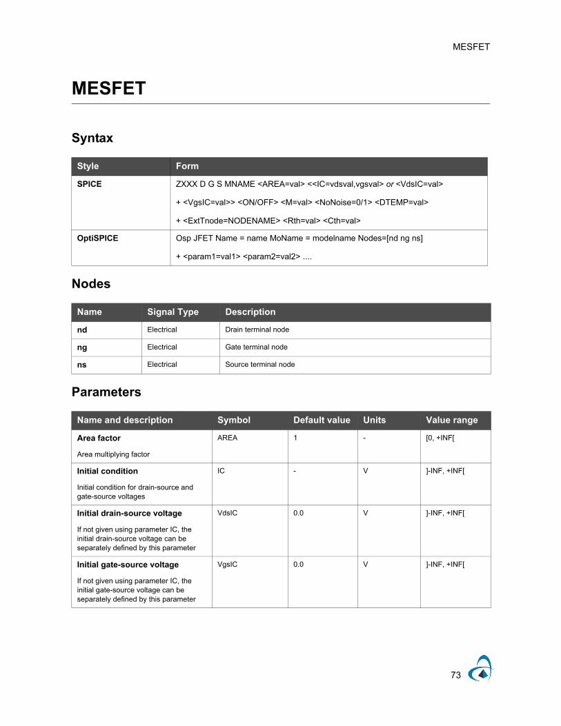
MESFET
73
MESFET
Syntax
Nodes
Electrical Drain terminal node
Electrical Gate terminal node
Electrical Source terminal node
Parameters
Style Form
SPICE ZXXX D G S MNAME <AREA=val> <<IC=vdsval,vgsval> or <VdsIC=val>
+ <VgsIC=val>> <ON/OFF> <M=val> <NoNoise=0/1> <DTEMP=val>
+ <ExtTnode=NODENAME> <Rth=val> <Cth=val>
OptiSPICE Osp JFET Name = name MoName = modelname Nodes=[nd ng ns]
+ <param1=val1> <param2=val2> ....
Name Signal Type Description
nd
ng
ns
Name and description Symbol Default value Units Value range
Area factor
Area multiplying factor
AREA 1 - [0, +INF[
Initial condition
Initial condition for drain-source and gate-source voltages
IC - V ]-INF, +INF[
Initial drain-source voltage
If not given using parameter IC, the initial drain-source voltage can be separately defined by this parameter
VdsIC 0.0 V ]-INF, +INF[
Initial gate-source voltage
If not given using parameter IC, the initial gate-source voltage can be separately defined by this parameter
VgsIC 0.0 V ]-INF, +INF[

MESFET
74
Technical Background
The element MESFET is the Metal Semiconductor Field Effect Transistor. For more
details see Technical Background of MESFET Model.
Example
For a n-channel MESFET with a device name Zn connected to nodes VDD, VI, and VSS, with model name NMFMOD netlist statement can be given by
Zn VDD VI VSS NMFMOD
Set initial condition
Set initial condition to set the initial DC values
ON/OFF ON - [ON, OFF]
Multiplier
Multiplier to simulate parallel elements
M 1 - [1, +INF[
Exclude Noise
Exclude element noise (1) or not (0)
NoNoise 0 - ]-INF, +INF[
Temperature difference
The temperature difference between the element and the circuit
DTEMP 0 K ]-INF, +INF[
Temperature node
The name of the external temperature node
ExtTNode - - -
Thermal resistance
Thermal resistance of element
Rth 0 K/W [0, +INF[
Thermal capacitance
Thermal capacitance of element
Cth 0 W sec/K [0, +INF[
Name and description Symbol Default value Units Value range

75
Optoelectronic Elements Library
This section contains information on the following elements
• CWSOURCE
• LASER
• MACHZEHNDER
• OPTELECABS
• OPTPHASEDELAY
• PHOTODIODE
• LED

76
Notes:

CWSOURCE
77
CWSOURCE
Syntax
Nodes
Electrical Input voltage node controlling magnitude
Electrical Input voltage node controlling phase
Optical Optical output
Parameters
Style Form
OptiSPICE Osp CWSOURCE Name=ELEMENT_NAME Nodes=[n1 n2 Output]+ MoName=MODEL_NAME <Wavelength=val> <Frequency=val>+ <FrequencyUnit=Hz/THz/nm> <FreqShift=val>+ <GainCoeff=val> <PhaseCoeff=val> + <RealEfieldCoeff=val> <ImagEfieldCoeff=val>+ <dPhidt_DC=val> <CarrierFreqNode=NODE_NAME>
Name Signal Type Description
n1
n2
Output
Name and description Symbol Default value Units Value range
Wavelength
Wavelength
Wavelength 1550 nm [0, +INF[
Frequency
Center frequency
Frequency 193.1 - [0, +INF[
Frequency unit
Channel frequency unit
FrequencyUnit THz - Hz, THz, nm
Frequency shift
Carrier Frequency offset of the source
FreqShift 0.0 - [0, +INF[
Gain coefficient
Output optical signal gain coefficient
GainCoeff 1.0 - ]-iNF +INF[
Phase coefficient
Output optical signal phase coefficient
PhaseCoeff 1.0 - ]-iNF +INF[

CWSOURCE
78
Technical Background
Generates a continuous wave (CW) optical signal controlled by electrical inputs.
CWSOURCE model is used to model this element. For more details see Technical
Background of CWSOURCE Model.
Example
For a CW laser with device name CW1, model CWModel, connected to nodes SIG1,
SIG2 and SIG3, with center frequency of 193.1 THz the netlist statement can be given
by
Osp CWSOURCE Name=CW1 Nodes=[SIG1 SIG2 SIG3] MoName=CWModel
+ Frequency=193.1 FrequencyUnit=THz
Real electric field coefficient
Coefficient for real part of the output electric field
RealEfieldCoeff 1.0 V/m ]-iNF +INF[
Imaginary electric field coefficient
Coefficient for imaginary part of the output electric field
ImagEfieldCoeff 1.0 - ]-iNF +INF[
DC phase slope
Slope of the phase at DC
dPhidt_DC 0 rad/s ]-iNF +INF[
Carrier frequency node
External node to input varying carrier frequency value
CarrierFreqNode - - -
Name and description Symbol Default value Units Value range

LASER
79
LASER
Syntax
Nodes
Electrical Laser diode positive node
Electrical Laser diode negative node
Optical Optical output
Parameters
Style Form
OptiSPICE Osp LASER Name=ELEMENT_NAME Nodes=[n1 n2 Output]+ MoName=MODEL_NAME <Wavelength=val> <Frequency=val>+ <FrequencyUnit=Hz/THz/nm> <FreqShift=val> <InitId=val>+ <Rth=val> <Cth=val> <DTEMP=val> <ExtTNode=NODE_NAME>+ <NoNoise=0/1>
Name Signal Type Description
n1
n2
Output
Name and description Symbol Default value Units Value range
Wavelength
Laser wavelength
Wavelength 1550 nm [0, +INF[
Frequency
Center frequency
Frequency 193.1 - [0, +INF[
Frequency Unit
Frequency unit selection
FrequencyUnit THz - Hz, THz, nm
Frequency Shift
Carrier Frequency Offset of the source
FreqShift 0.0 - [0, +INF[
Initial DC Current
Initial condition of DC current
InitId -1 A -INF, +INF[
Thermal resistance
Thermal resistance of the element
Rth 0 K/W [0, +INF[
Thermal capacitance
Thermal capacitance of the element
Cth 0 J/K [0, +INF[

LASER
80
Technical Background
An optical element that uses stimulated emission of radiation to generate EM waves,
based on laser rate-equations. A LASER model is used to model this element. For
more details see Technical Background of LASER model.
Example
For a Laser with device name LS1, model LSModel, connected to nodes SIG1, SIG2 and SIG3, with center frequency of 193.1 THz the netlist statement can be given by
Osp LASER Name=LS1 Nodes=[SIG1 SIG2 SIG3] MoName=LSModel
+ Frequency=193.1 FrequencyUnit=THz
Temperature difference
The temperature difference between the element and the circuit
DTEMP 0 K ]-INF, +INF[
Temperature node
The name of the external temperature node
ExtTNode - - -
Exclude noise
Exclude element noise (1) or not (0)
NoNoise 0 - 0, 1
Name and description Symbol Default value Units Value range

MACHZEHNDER
81
MACHZEHNDER
Syntax
Nodes
Optical Optical in
Optical Optical out
Control Nodes (CNodes)
Electrical Node for controlling RF voltage 1
Electrical Node for controlling RF voltage 2
Bias Nodes (BNodes)
Electrical Node for bias voltage 1
Electrical Node for bias voltage 2
Parameters
Style Form
OptiSPICE Osp MACHZEHNDER Name=ELEMENT_NAME Nodes=[Input Output]+ CNodes=[RF1 RF2] BNodes=[Bias1 Bais2]+ MoName=MODEL_NAME <Rth=val> <Cth=val> <DTEMP=val>+ <ExtTNode=NODE_NAME> <NoNoise=0/1>
Name Signal Type Description
Input
Output
Name Signal Type Description
RF1
RF2
Name Signal Type Description
Bias1
Bias2
Name and description Symbol Default value Units Value range
Extinction ratio
Extinction ratio of the modulator in dB
ExtinctionRatio 20 dB ]0, +INF[
Switching bias voltage
DC voltage required to turn the modulator from the OFF state to the ON state, or vice versa
SwitchBiasVoltage 4 V ]0, +INF[

MACHZEHNDER
82
Technical Background
This element is an Mach-Zehnder modulator which consists of an input optical
branch, which splits the incoming light into two arms, followed by two independent
optical arms, which are subsequently recombined by the output optical branch.
MACHZEHNDER model is used to model this element. For more details see
Technical Background of MACHZEHNDER model.
Example
For a modulator with device name MZ1, model MZModel, connected to optical nodes
SIG1 and SIG2, RF nodes SIG3 and SIG4, and bias nodes SIG5 and SIG6 with
extinction ratio of 20 dB, switching bias voltage 4.5V, switching RF voltage of 4.5V,
and insertion loss of 3dB, the netlist statement can be given by
Osp MACHZEHNDER Name=MZ1 Nodes=[SIG1 SIG2] CNodes=[SIG3 SIG4]
+ BNodes=[SIG5 SIG6] MoName=MZModel ExtinctionRatio=20
+ SwitchBiasVoltage=4.5 SwitchRFVoltage=4.5 InsertionLoss=3
Switching RF voltage
RF voltage required to turn the modulator from the OFF state to the ON state, or vice versa
SwitchRFVoltage 4 V ]0, +INF[
Insertion loss
The insertion loss of the Machzehdner interferometer
InsertionLoss 5 dB ]0, +INF[
Thermal resistance
Thermal resistance of the element
Rth 0 K/W [0, +INF[
Thermal capacitance
Thermal capacitance of the element
Cth 0 J/K [0, +INF[
Temperature difference
The temperature difference between the element and the circuit
DTEMP 0 K ]-INF, +INF[
Temperature node
The name of the external temperature node
ExtTNode - - -
Exclude noise
Exclude element noise (1) or not (0)
NoNoise 0 - 0, 1
Name and description Symbol Default value Units Value range

OPTELECABS
83
OPTELECABS
Syntax
Nodes
Optical Optical input
Optical Optical output
Control Nodes (CNodes)
Electrical Control voltage positive node
Electrical Control voltage negative node
Parameters
Style Form
OptiSPICE Osp OPTELECABS Name=ELEMENT_NAME Nodes=[Input Output]+ CNodes=[Control1 Control2] MoName=MODEL_NAME+ <InitId=val> <Rth=val> <Cth=val>+ <DTEMP=val> <ExtTNode=NODE_NAME> <NoNoise=0/1>
Name Signal Type Description
Input
Output
Name Signal Type Description
Control1
Control2
Name and description Symbol Default value Units Value range
Initial Current
Initial current of opto electronic absorber
InitId -1 A ]-INF, +INF[
Thermal resistance
Thermal resistance of the element
Rth 0 K/W [0, +INF[
Thermal capacitance
Thermal capacitance of the element
Cth 0 J/K [0, +INF[
Temperature difference
The temperature difference between the element and the circuit
DTEMP 0 K ]-INF, +INF[

OPTELECABS
84
Technical Background
This element is an electroabsorption modulator which is typically used to modulate a
constant amplitude optical source to produce a bit stream. OPTELECABS model
statement is used to model this element. For more details see Technical Background
of OPTELECABS Model.
Example
For a modulator with device name EA1, model EAModel, connected to nodes SIG1,
and SIG2, and controlled by nodes SIG3 and SIG4, the netlist statement can be given
by
Osp OPTELECABS Name=EA1 Nodes=[SIG1 SIG2] CNodes=[SIG3 SIG4]
+ MoName=EAModel
Temperature node
The name of the external temperature node
ExtTNode - - -
Exclude noise
Exclude element noise (1) or not (0)
NoNoise 0 - 0, 1
Name and description Symbol Default value Units Value range

OPTPHASEDELAY
85
OPTPHASEDELAY
Syntax
Nodes
Optical Optical input
Optical Optical output
Control Nodes (CNodes)
Electrical Phase delay controlling voltage positive node
Electrical Phase delay controlling voltage negative node
Parameters
Style Form
OptiSPICE Osp OPTPHASEDELAY Name=ELEMENT_NAME Nodes=[Input Output]+ CNodes=[Control1 Control2] MoName=MODEL_NAME+ <PhaseDelay=val> <Gain=val> <Rth=val> <Cth=val>+ <DTEMP=val> <ExtTNode=NODE_NAME> <NoNoise=0/1>
Name Signal Type Description
Input
Output
Name Signal Type Description
Control1
Control2
Name and description Symbol Default value Units Value range
Phase Delay
The option allows the user to define the optical phase delay
PhaseDelay 0 Rad ]-INF, +INF[
Gain
The option allows the user to define the gain of the optical phase delay, default is unity
Gain 1.0 - ]-INF, +INF[
Thermal resistance
Thermal resistance of the element
Rth 0 K/W [0, +INF[
Thermal capacitance
Thermal capacitance of the element
Cth 0 J/K [0, +INF[

OPTPHASEDELAY
86
Technical Background
A optical element that adds phase shift to the optical field. See Technical Background
of OPTPHASEDELAY Model for more details.
Examples
For a phase delay with element name OP1, model OPModel, connected to nodes
SIG1 and SIG2, and controlled by SIG3 and SIG4, the netlist statement can be given
by
Osp OPTPHASEDELAY Name=OP1 Nodes=[SIG1 SIG2] CNodes=[SIG3 SIG4]
+ MoName=OPModel
Temperature difference
The temperature difference between the element and the circuit
DTEMP 0 K ]-INF, +INF[
Temperature node
The name of the external temperature node
ExtTNode - - -
Exclude noise
Exclude element noise (1) or not (0)
NoNoise 0 - 0, 1
Name and description Symbol Default value Units Value range

PHOTODIODE
87
PHOTODIODE
Syntax
Nodes
Optical Optical input
Electrical Diode positive node
Electrical Diode negative node
Parameters
Thermal resistance
Thermal resistance of the element
Rth 0 K/W [0, +INF[
Thermal capacitance
Thermal capacitance of the element
Cth 0 J/K [0, +INF[
Temperature difference
The temperature difference between the element and the circuit
DTEMP 0 K ]-INF, +INF[
Temperature node
The name of the external temperature node
ExtTNode - - -
Exclude noise
Exclude element noise (1) or not (0)
NoNoise 0 - 0, 1
Technical Background
Photodiode is an element that converts light into an electrical signal. PHOTODIODE
Model statement is used to model this element. For more details see Technical
Background of PHOTODIODE Model.
Style Form
OptiSPICE Osp PHOTODIODE Name=ELEMENT_NAME Nodes=[Input n1 n2]+ MoName=MODEL_NAME <Rth=val> <Cth=val> <DTEMP=val>+ <ExtTNode=NODE_NAME> <NoNoise=0/1>
Name Signal Type Description
Input
n1
n2
Name and description Symbol Default value Units Value range

PHOTODIODE
88
Example
For a phase delay with device name PD1, model PDModel, connected to nodes SIG1,
SIG2 and SIG3, the netlist statement can be given by
Osp PHOTODIODE Name=PD1 Nodes=[SIG1 SIG2 SIG3] MoName=PDModel

LED
89
LED
Syntax
Nodes
Electrical Diode positive node
Electrical Diode negative node
Optical Optical output
Parameters
Style Form
OptiSPICE Osp LED Name=ELEMENT_NAME Nodes=[n1 n2 Output]+ MoName=MODEL_NAME <Frequency=val> <Bandwidth=val>+ <FrequencyUnit=Hz/THz/nm> <Rth=val> <Cth=val>+ <DTEMP=val> <ExtTNode=NODE_NAME> <NoNoise=0/1>
Name Signal Type Description
n1
n2
Output
Name and description Symbol Default value Units Value range
Frequency
Center frequency
Frequency 193.1 - [0, +INF[
Bandwidth
3-dB bandwidth
Bandwidth 6 - [0, +INF[
Frequency Unit
Frequency unit selection
FrequencyUnit THz - Hz, THz, nm
Thermal resistance
Thermal resistance of the element
Rth 0 K/W [0, +INF[
Thermal capacitance
Thermal capacitance of the element
Cth 0 J/K [0, +INF[
Temperature difference
The temperature difference between the element and the circuit
DTEMP 0 K ]-INF, +INF[
Temperature node
The name of the external temperature node
ExtTNode - - -

LED
90
Technical Background
This element simulates Light Emitting Diode (LED). A LED model is used to model
this element. This element only works for transient analysis with noise enabled. For
more details see Technical Background of LED model.
Example
For a LED with device name led1, model LEDModel, connected to nodes Vp, Vm and Lout, with center wavelength of 650 nm and a 3-dB bandwidth of 30 nm, the netlist statement can be given by
Osp LED Name=LS1 Nodes=[Vp Vm Lout] MoName=LEDModel
+ Frequency=650 Bandwidth=30 FrequencyUnit=nm
Exclude noise
Exclude element noise (1) or not (0)
NoNoise 0 - 0, 1
Name and description Symbol Default value Units Value range
91
Optical Elements Library
This section contains information on the following elements
• OPTGAIN
• XCOUPLER
• SMFIBER
• MMFIBER
• FREESPACE
• OCONN (OPTISO, POLARIZER)
• OPTCIRC
• MIRROR
• SPLITTER
• OMNIOCONN
• OPTCHANNELFILTER
• OPTFFT
• MULTILAYERFILTER
• WAVEGUIDE
• OPTRING
• OPTISYSINOPT

92
Notes:

OPTGAIN
93
OPTGAIN
Syntax
Osp OPTGAIN Name=ELEMENT_NAME Nodes=[Input Output]
+ MoName=MODEL_NAME <Gain=val> <Atten=val> <RevGain=val>
+ <RevAtten=val> <GaindB=val> <AttendB=val> <RevGaindB=val>
+ <RevAttendB=val> <PhaseShift=val> <RevPhaseShift=val>
+ <Rth=val> <Cth=val> <DTEMP=val> <ExtTNode=NODE_NAME>
+ <NoNoise=0/1>
Nodes
Optical
Optical
Parameters
Style Form
OptiSPICE
Name Signal Type Description-
Input
Output
Name and description Symbol Default value Units Value range
Gain
Power gain factor (port 1 to port 2)
Gain 1 - ]-INF, +INF[
Attenuation
Power loss factor (port 1 to port 2)
Atten 1 - ]-INF, +INF[
Reverse gain
Power gain factor (port 2 to port 1)
RevGain 1 - ]-INF, +INF[
Reverse attenuation
Power loss factor (port 2 to port 1)
RevAtten 1 - ]-INF, +INF[
Gain in dB
Power gain in dB (port 1 to port 2)
GaindB 0 dB ]-INF, +INF[
Attenuation in dB
Power loss in dB (port 1 to port 2)
AttendB 0 dB ]-INF, +INF[
Reverse gain in dB
Power gain in dB (port 2 to port 1)
RevGaindB 0 dB ]-INF, +INF[

OPTGAIN
94
Technical Background
This element amplifies the optical signal power. The attenuation or gain of the element
can be specified by using Gain/Atten/RevGain/RevAtten and corresponding dB
parameters (GaindB, AttendB, etc.). For more details see Technical Background of
OPTGAIN model.
Example
For a gain device with name OA1, model OGModel, connected to nodes SIG1 and SIG2, with 3 dB of forward gain, -100 dB of reverse gain, forward noise figure of 6 dB, and reverse noise figure of -100 dB, the netlist statement can be given by
Osp OPTGAIN Name=OA1 Nodes=[SIG1 SIG2] MoName=OGModel GaindB=3
Reverse attenuation in dB
Power loss in db (port 2 to port 1)
RevAttendB 0 dB ]-INF, +INF[
Noise figure
Determines the amplifier noise figure (port 1 to port 2)
NoiseFigure 0 dB ]-INF, +INF[
Reverse Noise figure
Determines the amplifier noise figure (port 2 to port 1)
RevNoiseFigure 0 dB ]-INF, +INF[
Phase shift
Phase shift (port 1 to port 2)
PhaseShift 0 rad ]-INF, +INF[
Reverse phase shift
Phase shift (port 2 to port 1)
RevPhaseShift 0 rad ]-INF, +INF[
Thermal resistance
Thermal resistance of the element
Rth 0 K/W [0, +INF[
Thermal capacitance
Thermal capacitance of the element
Cth 0 J/K [0, +INF[
Temperature difference
The temperature difference between the element and the circuit
DTEMP 0 K ]-INF, +INF[
Temperature node
The name of the external temperature node
ExtTNode - - -
Exclude noise
Exclude element noise (1) or not (0)
NoNoise 0 - 0, 1
Name and description Symbol Default value Units Value range

OPTGAIN
95
+ RevGaindB=-100 NoiseFigure=6 RevNoiseFigure=-100

OPTGAIN
96
Notes:

XCOUPLER
97
XCOUPLER
Syntax
Osp XCOUPLER Name=ELEMENT_NAME Nodes=[in1 in2 out1 out2]
+ MoName=MODEL_NAME <C=val> <Conjugate=0/1> <Rth=val> <Cth=val>
+ <DTEMP=val> <ExtTNode=NODE_NAME> <NoNoise=0/1>
Nodes
Optical Input 1
Optical Input 2
Optical Output 1
Optical Output 2
Parameters
Style Form
OptiSPICE
Name Signal Type Description
in1
in2
out1
out2
Name and description Symbol Default value Units Value range
Coupling Ratio
Coupled power ratio between the input and output optical pairs
C 0.5 - [0, 1]
Input/Output Conjugate
The option allows the user to specify which the inputs/outputs pair conjugates
Conjugate 1 - 0, 1
Thermal resistance
Thermal resistance of the element
Rth 0 K/W [0, +INF[
Thermal capacitance
Thermal capacitance of the element
Cth 0 J/K [0, +INF[
Temperature difference
The temperature difference between the element and the circuit
DTEMP 0 K ]-INF, +INF[
Temperature node
The name of the external temperature node
ExtTNode - - -

XCOUPLER
98
Technical Background
An optical cross-coupler is a device that physically couples two input signals and
produces two output signals. For more details see Technical Background of
XCOUPLER model.
Example
For a cross coupler with device name XC1, model XCModel, connected to nodes
SIG1, SIG2, SIG3 and SIG4, with 0.5 coupling coefficient and conjugate mode
enabled, the netlist statement can be given by
Osp XCOUPLER Name=XC1 Nodes=[SIG1 SIG2 SIG3 SIG4] MoName=XCModel C=0.5
+ Conjugate=1
Exclude noise
Exclude element noise (1) or not (0)
NoNoise 0 - 0, 1
Name and description Symbol Default value Units Value range

SMFIBER
99
SMFIBER
Syntax
Osp SMFIBER Name=ELEMENT_NAME Nodes=[Input Output]
+ MoName=MODEL_NAME <Length=val> <Rth=val> <Cth=val>
+ <DTEMP=val> <ExtTNode=NODE_NAME> <NoNoise=0/1>
Nodes
Optical
Optical
Parameters
Length
Fiber length
Length 10 km [0, +INF[
Thermal resistance
Thermal resistance of the element
Rth 0 K/W [0, +INF[
Thermal capacitance
Thermal capacitance of the element
Cth 0 J/K [0, +INF[
Temperature difference
The temperature difference between the element and the circuit
DTEMP 0 K ]-INF, +INF[
Temperature Node
The name of the external temperature node
ExtTNode - - -
Exclude noise
Exclude element noise (1) or not (0)
NoNoise 0 - 0, 1
Technical Background
The SM Fiber element simulates the propagation of an optical field in a single-mode
fiber with the dispersive and nonlinear effects taken into account by a direct numerical
Style Form
OptiSPICE
Name Signal Type Description
Input
Output
Name and description Symbol Default value Units Value range

SMFIBER
100
integration of the modified nonlinear Schrödinger (NLS) equation. For more details
see Technical Background of SMFIBER Model.
Example
For a fiber with device name SM1, model SMFModel, connected to nodes SIG1 and
SIG2, with 1 km, the netlist statement can be given by
Osp SMFIBER Name=SM1 Nodes=[SIG1 SIG2] MoName=SMFModel Length=1

MMFIBER
101
MMFIBER
Syntax
Osp MMFIBER Name=ELEMENT_NAME Nodes=[Input Output]
+ MoName=MODEL_NAME <Length=val> <Rth=val> <Cth=val>
+ <DTEMP=val> <ExtTNode=NODE_NAME> <NoNoise=0/1>
Nodes
Optical
Optical
Parameters
Length
Fiber length
Length 0 km [0, +INF[
Thermal resistance
Thermal resistance of the element
Rth 0 K/W [0, +INF[
Thermal capacitance
Thermal capacitance of the element
Cth 0 J/K [0, +INF[
Temperature difference
The temperature difference between the element and the circuit
DTEMP 0 K ]-INF, +INF[
Temperature Node
The name of the external temperature node
ExtTNode - - -
Exclude noise
Exclude element noise (1) or not (0)
NoNoise 0 - 0, 1
Style Form
OptiSPICE
Name Signal Type Description
Input
Output
Name and description Symbol Default value Units Value range

MMFIBER
102
Technical Background
This element is a multimode fiber. It is a spatially dependent device that models the
transverse field profiles and propagation constants for each mode supported by the
fiber. For more details see Technical Background of MMFIBER Model.
Example
For a fiber with device name MMF1, model MMFModel, connected to nodes SIG1 and
SIG2, with 1 km, the netlist statement can be given by
Osp MMFFIBER Name=MMF1 Nodes=[SIG1 SIG2] MoName=MMFModel Length=1

FREESPACE
103
FREESPACE
Syntax
Nodes
Optical
Optical
Parameters
Style Form
OptiSPICE Osp FREESPACE Name=ELEMENT_NAME Nodes=[Input Output]+ MoName=MODEL_NAME <D=val> <XOff=val> <YOff=val>+ <XTilt=val> <YTilt=val> <Rth=val> <Cth=val>+ <DTEMP=val> <ExtTnode=val> <NoNoise=0/1>
Name Signal Type Description
Input
Output
Name and description Symbol Default value Units Value range
Distance
Freespace distance
D 0 m [0, +INF[
X offset
Defines the amount of translation of the mode shape in the X-direction
XOff 0 um [0, +INF[
Y offset
Defines the amount of translation of the mode profile in the Y-direction
YOff 0 um [0, +INF[
X tilt
Defines the amount of rotation of the mode profile around the X-axis
XTilt 0 rad ]-INF, +INF[
Y tilt
Defines the amount of rotation of the mode profile around the Y-axis
YTilt 0 rad ]-INF, +INF[
Thermal resistance
Thermal resistance of the element
Rth 0 K/W [0, +INF[

FREESPACE
104
Technical Background
Freespace devices represent the optical connection formed between two devices with
possibly different mode structures where a region of free-space is present at the
interface. For more details see Technical Background of FREESPACE Model.
Example
For a free space propagation with device name FSO1, model FSOModel, connected
to nodes SIG1 and SIG2, with a distance of 10 um, the netlist statement can be given
by
Osp FREESPACE Name=FSO1 Nodes=[SIG1 SIG2] MoName=FSOModel D=10u
Thermal capacitance
Thermal capacitance of the element
Cth 0 J/K [0, +INF[
Temperature difference
The temperature difference between the element and the circuit
DTEMP 0 K ]-INF, +INF[
Temperature node
The name of the external temperature node
ExtTNode - - -
Exclude noise
Exclude element noise (1) or not (0)
NoNoise 0 - 0, 1
Name and description Symbol Default value Units Value range

OCONN (OPTISO, POLARIZER)
105
OCONN (OPTISO, POLARIZER)
Syntax
Osp OCONN Name=ELEMENT_NAME Nodes=[Input Output]
+ MoName=MODEL_NAME <Ref=val> <RevRef=val> <RefdB=val>
+ <RevRefdB=val> <PhaseShift=val> <RevPhaseShift=val>
+ <RefPhaseShift=val> <RevRefPhaseShift=val> <Gain=val>
+ <RevGain=val> <Atten=val> <RevAtten=val> <XOff=val>
+ <YOff=val> <XTilt=val> <YTilt=val> <GaindB=val>
+ <RevGaindB=val> <AttendB=val> <RevAttendB=val>
+ <PolarMode=None/X/Y/Am45/...> <JonesMatrix=[val1 val2 ...]>
+ <PolAngle=val> <CNodes=[Control1 Control2]>
+ <IsoMode=FWD/REV> <Rth=val><Cth=val> <DTEMP=val>
+ <ExtTNode=NODE_NAME> <NoNoise=0/1>
Nodes
Optical
Optical
Parameters
Style Form
OptiSPICE
Name Signal Type Description
Input
Output
Name and description Symbol Default value Units Value range
Reflection
Power return loss (port 1 to port 1)
Ref 0 - ]-INF, +INF[
Reverse reflection
Power return loss (port 2 to port 2)
RevRef 0 - ]-INF, +INF[
Reflection in dB
Power return loss (port 1 to port 1) in dB
RefdB 100 dB ]-INF, +INF[
Reverse reflection in dB
Power return loss (port 2 to port 2) in dB
RevRefdB 100 dB ]-INF, +INF[
Forward phase shift
Phase shift (port 1 to port 2)
PhaseShift 0 rag ]-INF, +INF[

OCONN (OPTISO, POLARIZER)
106
Reverse phase shift
Phase shift (port 2 to port 1)
RevPhaseShift 0 rad ]-INF, +INF[
Return phase shift
Phase shift (port 1 to port 1)
RefPhaseShift pi/2 rad ]-INF, +INF[
Reverse return phase shift
Phase shift (port 2 to port 2)
RevRefPhaseShift pi/2 rad ]-INF, +INF[
Gain
Power gain factor (port 1 to port 2)
Gain 1 - ]-INF, +INF[
Reverse gain
Power gain factor (port 2 to port 1)
RevGain 1 - ]-INF, +INF[
Attenuation
Power loss factor (port 1 to port 2)
Atten 1 - ]-INF, +INF[
Reverse attenuation
Power loss factor (port 2 to port 1)
RevAtten 1 - ]-INF, +INF[
Gain in dB
Power gain in dB (port 1 to port 2)
GaindB (FwdGaindB)
0 dB ]-INF, +INF[
Reverse gain in dB
Power gain in dB (port 2 to port 1)
RevGaindB 0 dB ]-INF, +INF[
Attenuation in dB
Power loss in dB (port 1 to port 2)
AttendB (FwdAttendB)
0 dB ]-INF, +INF[
Reverse attenuation in dB
Power loss in dB (port 2 to port 1)
RevAttendB 0 dB ]-INF, +INF[
X offset
Defines the amount of translation of the mode shape in the X-direction
XOff 0 um [0, +INF[
Y offset
Defines the amount of translation of the mode profile in the Y-direction
YOff 0 um [0, +INF[
X tilt
Defines the amount of rotation of the mode profile around the X-axis
XTilt 0 rad ]-INF, +INF[
Y tilt
Defines the amount of rotation of the mode profile around the Y-axis
YTilt 0 rad ]-INF, +INF[
Name and description Symbol Default value Units Value range

OCONN (OPTISO, POLARIZER)
107
Technical Background
This element is an optical connector/isolator used to connect two elements with
differing mode shapes, the mode shapes of the two elements will be used to calculate
the mode mixing for signals travelling between the two elements using overlap
integrals. For more details see Technical Background of OCONN Model.
Isolation mode
Direction of Isolation for optical connection
IsoMode FWD - FWD, REV
Polar mode
Polar mode type
PolarMode - - None, X, Y, A45, Am45, Angle, LeftCir, RightCir, QWPX, QWPY, HWPX, HWPY, VDEP
Control nodes
Nodes to control polarization if PolarMode is VDEP
CNodes - - -
Jones matrix coefficients
Jones Matrix coefficients -- J11.r J11.i J12.r J12.i J21.r J21.i J22.r J22.i
JonesMatrix - - ]-INF, +INF[
Polarization rotation
Polarization rotation angle
PolAngle 0 rad ]-INF, +INF[
Thermal resistance
Thermal resistance of the element
Rth 0 K/W [0, +INF[
Thermal capacitance
Thermal capacitance of the element
Cth 0 J/K [0, +INF[
Temperature difference
The temperature difference between the element and the circuit
DTEMP 0 K ]-INF, +INF[
Temperature Node
The name of the external temperature node
ExtTNode - - -
Exclude noise
Exclude element noise (1) or not (0)
NoNoise 0 - 0, 1
Name and description Symbol Default value Units Value range

OCONN (OPTISO, POLARIZER)
108
Example
For a connector with name OC1, model OCModel, connected to nodes SIG1 and
SIG2, with attenuation of of 0.5 dB, the netlist statement can be given by
Osp OCONN Name=OC1 Nodes=[SIG1 SIG2] MoName=OCModel AttendB=0.5
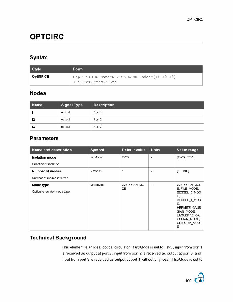
OPTCIRC
109
OPTCIRC
Syntax
Nodes
optical Port 1
optical Port 2
optical Port 3
Parameters
Isolation mode
Direction of isolation
IsoMode FWD - [FWD, REV]
Number of modes
Number of modes involved
Nmodes 1 - [0, +INF[
Mode type
Optical circulator mode type
Modetype GAUSSIAN_MODE
- GAUSSIAN_MODE, FILE_MODE, BESSEL_0_MODE, BESSEL_1_MODE, HERMITE_GAUSSIAN_MODE, LAGUERRE_GAUSSIAN_MODE, UNIFORM_MODE
Technical Background
This element is an ideal optical circulator. If IsoMode is set to FWD, input from port 1
is received as output at port 2, input from port 2 is received as output at port 3, and
input from port 3 is received as output at port 1 without any loss. If IsoMode is set to
Style Form
OptiSPICE Osp OPTCIRC Name=DEVICE_NAME Nodes=[I1 I2 I3]+ <IsoMode=FWD/REV>
Name Signal Type Description
I1
I2
I3
Name and description Symbol Default value Units Value range

OPTCIRC
110
REV, input from port 1 is received as output at port 3, input from port 3 is received as
output at port 2, and input from port 2 is received as output at port 1 without any loss.
This element do not require any model statement.
Example
For a circulator with name OC1, connected to nodes SIG1, SIG2 and SIG3, working
with clockwise direction, the netlist statement can be given by
Osp OPTCIRC Name=OC1 Nodes=[SIG1 SIG2 SIG3]

MIRROR
111
MIRROR
Syntax
Nodes
Optical Mirror node for incident and reflected optical signal
Parameters
Style Form
OptiSPICE Osp MIRROR Name=ELEMENT_NAME Nodes=[Inout]+ MoName=MODEL_NAME <Ref=val> <RefdB=val>+ <PhaseShift=val> <Rth=val> <Cth=val> <DTEMP=val>+ <ExtTNode=NODE_NAME> <NoNoise=0/1>
Name Signal Type Description
Inout
Name and description Symbol Default value Units Value range
Reflection coefficient
Ratio of reflected power from mirror
Ref 0 - ]-INF, +INF[
Reflection coefficient in dB
Ratio of reflected power from mirror in dB
RefdB 100 dB ]-INF, +INF[
Phase shift
Phase shift of reflected wave
PhaseShift 0 rad ]-INF, +INF[
Thermal resistance
Thermal resistance of the element
Rth 0 K/W [0, +INF[
Thermal capacitance
Thermal capacitance of the element
Cth 0 J/K [0, +INF[
Temperature difference
The temperature difference between the element and the circuit
DTEMP 0 K ]-INF, +INF[
Temperature Node
The name of the external temperature node
ExtTNode - - -

MIRROR
112
Technical Background
The mirror simply reflects all incident modes and channels of whatever polarity is
incident from the input element. The parameters Ref and RefdB set the value of the
reflected power. The parameter PhaseShift sets the phase shift of the reflected wave.
For more details see MIRROR model.
Example
For an mirror with name OM1, model OMModel, connected to signal SIG1, with 50 %
reflection, the netlist statement can be given by
Osp MIRROR Name=OM1 Nodes=[SIG1] MoName=OMModel Ref=0.5
Exclude noise
Exclude element noise (1) or not (0)
NoNoise 0 - 0, 1
Name and description Symbol Default value Units Value range

SPLITTER
113
SPLITTER
Syntax
Nodes
Optical Splitter input port
Optical Splitter N output ports
Parameters
Split ratio
Power split ratio
SplitRatio 0.5 - [0, 1]
Thermal resistance
Thermal resistance of the element
Rth 0 K/W [0, +INF[
Thermal capacitance
Thermal capacitance of the element
Cth 0 J/K [0, +INF[
Temperature difference
The temperature difference between the element and the circuit
DTEMP 0 K ]-INF, +INF[
Temperature Node
The name of the external temperature node
ExtTNode - - -
Exclude noise
Exclude element noise (1) or not (0)
NoNoise 0 - 0, 1
Style Form
OptiSPICE Osp SPLITTER Name=ELEMENT_NAME Nodes=[in o1 o2 ... oN]+ MoName=MODEL_NAME <SplitRatio=val> + <Rth=val> <Cth=val> <DTEMP=val> <ExtTNode=NODE_NAME>+ <NoNoise=0/1>
Name Signal Type Description
in
o1, o2, ..., oN
Name and description Symbol Default value Units Value range

SPLITTER
114
Technical Background
This element represents an optical power splitter. It has one input port and a number
of (N) user given output ports. The model type required for this element is
OMNIOCONN. If the model parameter LossType is set to UNITY, input power is
simply duplicated at each output port. If the LossType is set to CONST_LOSS (default
choice), the power splitting has two cases: 1) if the number of output ports are two,
the parameter SplitRatio is used such that
where and are the powers at the output port 1 and 2 respectively and
is the input power; 2) if the number of output ports are more than two, the input power
will be split equally among for N output ports (1/N of the input power in each output
port). For more details see Technical Background of OMNIOCONN Model.
A splitter can also be used as a joiner if all output ports are used as inputs and input
port is used as an output.
Example
For an SPLITTER element with name SPT1, model SPTModel, connected to nodes
SIG1, SIG2 and SIG3, with 50% splitting ratio, the netlist statement can be given by
Osp SPLITTER Name=SPT1 Nodes=[SIG1 SIG2 SIG3] MoName=SPModel
+ SplitRatio=0.5
(1)
Po1 SplitRatio Pin=
Po2 1 SplitRatio– Pin=
Po1 Po2 Pin

OMNIOCONN
115
OMNIOCONN
Syntax
Input Nodes
Optical M input nodes
Output Nodes
Optical N output nodes
Parameters
Thermal resistance
Thermal resistance of the element
Rth 0 K/W [0, +INF[
Thermal capacitance
Thermal capacitance of the element
Cth 0 J/K [0, +INF[
Temperature difference
The temperature difference between the element and the circuit
DTEMP 0 K ]-INF, +INF[
Temperature Node
The name of the external temperature node
ExtTNode - - -
Exclude noise
Exclude element noise (1) or not (0)
NoNoise 0 - 0, 1
Style Form
OptiSPICE Osp OMNIOCONN Name=DEVICE_NAME InputNodes=[i1 i2 ... iM]+ OutputNodes=[o1 o2 ... oN] MoName=MODEL_NAME+ <Rth=val> <Cth=val> <DTEMP=val> <ExtTNode=NODE_NAME>+ <NoNoise=0/1>
Name Signal Type Description
i1, i2, ..., iM
Name Signal Type Description
o1, o2, ..., oN
Name and description Symbol Default value Units Value range

OMNIOCONN
116
Technical Background
This element can represent a general multi-input multi-output optical connector. For
more details see Technical Background of OMNIOCONN Model.
Example
For an OMNIOCONN element with name omc1, model Omodel, with five input ports
(in1,in2,..in5) and three output ports (out1, out2, and out3), the netlist statement can
be given by
Osp OMNIOCONN Name=omc1 InputNodes = [in1 in2 in3 in4 in5 ]
+ OutputNodes = [out1 out2 out3] MoName=Omodel

OPTCHANNELFILTER
117
OPTCHANNELFILTER
Syntax
Nodes
Optical
Optical
Parameters
Style Form
OptiSPICE Osp OPTCHANNELFILTER Name=ELEMENT_NAME + Nodes=[Input Output] MoName=MODEL_NAME + <PassBands=[val1 val2 ...]> <FrequencyUnit=Hz/THz/nm>+ <Bandwidth=val> <BandwidthUnit=Hz/GHz/nm>+ <PassBandMode=ListOfBands/CenterFreqAndBW/...>+ <Rth=val> <Cth=val> <DTEMP=val> <ExtTNode=NODE_NAME>+ <NoNoise=0/1>
Name Signal Type Description
Input
Output
Name and description Symbol Default value Units Value range
Frequency list
List of channel center frequencies
PassBands - - [0, +INF[
Frequency unit
Channel frequency unit
FrequencyUnit THz - Hz, THz, nm
Bandwidth
Channel bandwidth
Bandwidth 50 - [0, +INF[
Bandwidth unit
Channel bandwidth unit
BandwidthUnit GHz - Hz, GHz, nm
Passband mode
Passband mode selection to define the way center frequencies and bandwidths to be entered
PassBandMode ListOfBands - ListOfBands, CenterFreqAndBW, CenterFreqAndConstBW
Thermal resistance
Thermal resistance of the element
Rth 0 K/W [0, +INF[

OPTCHANNELFILTER
118
Technical Background
This element is an idealized optical filter used for allowing desired optical channels
while blocking unwanted channels. For more details see Technical Background of
OPTCHANNELFILTER Model.
Examples
For a channel filter with device name OF1, model OFModel, connected to nodes SIG1 and SIG2, filtering 193.1 THz and 193.2 THz, bandwidth of 50 GHz, the netlist statement can be given by
Osp OPTCHANNELFILTER Name=OF1 Nodes=[SIG1 SIG2]
+ MoName=OFModel PassBandMode=CenterFreqAndConstBW
+ PassBands=[193.1 193.2] FrequencyUnit=THz Bandwidth=50
+ BandwidthUnit=GHz
Thermal capacitance
Thermal capacitance of the element
Cth 0 J/K [0, +INF[
Temperature difference
The temperature difference between the element and the circuit
DTEMP 0 K ]-INF, +INF[
Temperature Node
The name of the external temperature node
ExtTNode - - -
Exclude noise
Exclude element noise (1) or not (0)
NoNoise 0 - 0, 1
Name and description Symbol Default value Units Value range

OPTFFT
119
OPTFFT
Syntax
Nodes
Optical Filter input
Optical Filter ouptut
Parameters
Style Form
OptiSPICE Osp OPTFFT Name=ELEMENT_NAME Nodes=[Input Output]+ MoName=MODEL_NAME <CenterFilterLambda=val> + <Frequency=val> <FilterFreqShift=val> + <FrequencyUnit=Hz/THz/nm> <DTEMP=val>+ <ExtTNode=NODE_NAME> <NoNoise=0/1>
Name Signal Type Description
Input
Output
Name and description Symbol Default value Units Value range
Frequency
Center frequency of the filter
Frequency 193.1 - [0, +INF[
Filter frequency shift
Frequency shift from center frequency value
FilterFreqShift 0 - [0, +INF[
Frequency unit
Frequency unit for Frequency and FilterFreqShift parameters
FrequencyUnit THz - Hz, THz, nm
Filter type
Filter transfer characteristics type
FilterType BESSEL - BESSEL, BUTTERWORTH
Bandwidth
3 dB filter bandwidth
FilterBW 10 GHz ]0,+INF[
Insertion loss
Insertion loss of the filter
FilterIL 0 dB [0,+INF[
Order
Order of the function
FilterOrder 1 - 1,2,3, ...

OPTFFT
120
Technical Background
OPTFFT element is an optical filter or frequency dependent element that can be either
a user defined filter type or a measured filter. User defined filter is defined by the
parameters: FilterType, FilterBW, FilterIL, and FilterOrder, while measured filter is
defined by parameters: FilterFile, FileFreqUnit, FileFormat and FilePowScale.
Measured filter can also be expressed using Touchstone file (tstonefile parameter).
For more details see Technical Background of OPTFFT Model.
Examples
For an optical Butterworth filter with the name OptFilter1 connected between nodes
in and out with center frequency 193.2 THz, 3-dB bandwidth of 50 GHz, filter order of
4, and insertion loss of 0.75 dB, the netlist statement can be written as
Osp OPTFFT Name=OptFilter1 Nodes=[in out] MoName=OPTFFTModel
Filter file
Filename with the measured data
FilterFile - - -
File frequency unit
Determines the frequency unit of the file with the measurements
FileFreqUnit Hz - Hz, GHz, THz, m, nm
File format
Determines the format of the file with the measurements
FileFormat POWERPHASE - POWERPHASE, REALIMAG
File power scale
Determines whether the measured data is in linear scale or in dB
FilePowScale LINEAR - LINEAR, DB
Touchstone file
Touchstone file name containing two port S-parameters for the optical filter
Tstonefile - - -
Temperature difference
The temperature difference between the element and the circuit
DTEMP 0 K ]-INF, +INF[
Temperature Node
The name of the external temperature node
ExtTNode - - -
Exclude noise
Exclude element noise (1) or not (0)
NoNoise 0 - 0, 1
Name and description Symbol Default value Units Value range

OPTFFT
121
+ Frequency=193.2 FrequencyUnit=THz FilterType=BUTTERWORTH
+ FilterBW=50 FilterOrder=4 FilterIL=0.75
For a measured filter given by a measured filter file ‘filter.dat’ where frequency unit is
given in nm and power is expressed in dB, the netlist statement can be written as
Osp OPTFFT Name=OptFilter2 Nodes=[in2 out2] MoName=OPTFFTModel
+ Frequency=193.2 FrequencyUnit=THz FilterFile=”filter.dat”
+ FileFreqUnit=nm FileFormat=POWERPHASE FilePowScale=DB
For an optical filter represented by a two port S-parameter given by a Touchstone file
‘filter.s2p’, the netlist statement can be written as
Osp OPTFFT Name=OptFilter3 Nodes=[in3 out3] MoName=OPTFFTModel
+ Frequency=193.4 FrequencyUnit=THz TstoneFile=”filter.s2p"

OPTFFT
122
Notes:

MULTILAYERFILTER
123
MULTILAYERFILTER
Syntax
Nodes
Optical Input
Optical Output
Parameters
Style Form
OptiSPICE Osp MULTILAYERFILTER Name=ELEMENT_NAME Nodes=[In Out]+ MoName=MODEL_NAME + <FilterCnodes=[{N1+ N1-} {N2+ N2-} ... {NL+ NL-}]> + <InitialVs=[vi1 vi2 ...viL]> + <FilterTnodes=[TN1 TN2 ... TNL]>+ <DefLambda=val> <InitialT=val> <DTemp=val>+ <ExtTNode=NODE_NAME> <Rth=val> <Cth=val>
Name Signal Type Description
In
Out
Name and description Symbol Default value Units Value range
List of connected voltage pairs to layers
List containing node names (in pairs) that are connected as controlling voltage for each layer
FilterCNodes - - -
Initial values for connected voltages
List containing initial voltage difference for the node pairs given by LayerCnodes
InitialVs - V ]-INF, +INF[
List of connected temperature nodes to layers
List containing temperature node names that set the temperature for each layer
FilterTNodes - - -
Defined wavelength
Unless channel wavelength is known from the source (laser,cw), this wavelength value is used to calculate the filter characteristics.
DefLambda 1550 nm ]0, +INF[

MULTILAYERFILTER
124
Technical Background
A multi-layer element is a thin film interference where the interference is often
exploited to produce filtering in optical systems. A multi-layer structure consisting of
layers of material of differing optical index will produce a complex series of interfering
waves formed by the reflection at and transmission through each interface. A
MULTILAYERFILTER model is used to characterize this element. For more details
see Technical Background of MULTILAYERFILTER Model.
Example
For a multi-layer filter with three layers connected to nodes in and out, represented by
model FilterEx, and controlled by an external voltage from node, vcnt, at the second
layer, the netlist statement can be written as follows:
Osp MultiLayerFilter Name=MLFilter Nodes=[in out] MoName=FilterEx
+ FilterCnodes=[{0 0} {vcnt 0} {0 0}]
Transmission line name
Name of the transmission line that controls the refractive indices of the multilayer filter.
TranslineName - - -
Expected rise in initial temperature
Initial expected temperature at t=0; used for robust DC convergence.
InitialT 0.0 C ]-INF, +INF[
Temperature difference
Temperature difference between the element and the circuit
DTemp 0.0 C ]-INF, +INF[
Temperature node
Name of the external temperature node. Only used if FilterTnodes are not given.
ExtTNode - - -
Thermal resistance
Thermal resistance of element
Rth 0 K/W [0, +INF[
Thermal capacitance
Thermal capacitance of element
Cth 0 W sec/K [0, +INF[
Name and description Symbol Default value Units Value range

WAVEGUIDE
125
WAVEGUIDE
Syntax
Nodes
Optical
Optical
Parameters
Style Form
OptiSPICE Osp WAVEGUIDE Name=DEVICE_NAME Nodes=[Input Output]+ MoName=MODEL_NAME <Neff=[n1 n2 ...nL]> <Length=val>+ <Atten=[a1 a2 ... aL]> <InitialT=val> <DTemp=val>+ <ExtTNode=NODE_NAME> <Rth=val> <Cth=val>
Name Signal Type Description
Input
Output
Name and description Symbol Default value Units Value range
List of mode effective indexes
List containing effective index for each mode of the waveguide
Neff - - ]0, +INF[
Waveguide length
Length of the waveguide
Length 1.0 um ]0, +INF[
List of mode attenuations
List containing attenuation for each mode
Atten - - ]0, +INF[
Expected rise in initial temperature
Initial expected temperature at t=0; used for robust DC convergence.
InitialT 0.0 C ]-INF, +INF[
Temperature difference
The temperature difference between the element and the circuit
DTemp 0.0 C ]-INF, +INF[
Temperature Node
The name of the external temperature node
ExtTNode - - -

WAVEGUIDE
126
Technical Background
A multi-mode waveguide element is similar to the multimode fiber element. However,
index can be modeled as temperature dependent. WAVEGUIDE model is used to
model the characteristics of the waveguide element since it supports multi-mode
device with a specified effective index for each mode. For more details see Technical
Background of MULTILAYERFLITER (WAVEGUIDE) Model.
Example
For a waveguide with device name WG, model WgModel, connected to nodes IN and
OUT, with the mode effective index of 1.47, length of 20 um, and attenuation of 0.95,
the netlist statement can be written as follows:
Osp WAVEGUIDE Name=WG Nodes=[IN OUT] MoName=WgModel
+ Neff=[1.47] Length=20 Atten = 0.95
Thermal resistance
Thermal resistance of element
Rth 0 K/W [0, +INF[
Thermal capacitance
Thermal capacitance of element
Cth 0 W sec/K [0, +INF[
Name and description Symbol Default value Units Value range

OPTRING
127
OPTRING
Syntax
Nodes
Optical Port 1
Optical Port 2
Optical Port 3
Optical Port 4
Parameters
Style Form
OptiSPICE Osp OPTRING Name=ELEM_NAME Nodes=[P1 P2 <P3 P4>]+ MoName=MODEL_NAME <Radius=val> <C<1>=val> <C2=val>+ <LayerCnodes=[{N1+ N1-} {N2+ N2-} ... {NL+ NL-}]> + <InitialVs=[vi1 vi2 ...viL]> + <LayerTnodes=[TN1 TN2 ... TNL]> <Conjugate<1>=0/1>+ <Conjugate2=0/1> <DefLambda=val> <InitialT=val>+ <DTemp=val> <ExtTNode=NODE_NAME> <Rth=val> <Cth=val>
Name Signal Type Description
P1
P2
P3
P4
Name and description Symbol Default value Units Value range
Radius
Radius of ring resonator
Radius 10 um ]0, +INF[
Coupling coefficient for XCoupler 1
Coupling ratio for the cross coupler
C1 0.5 - [0, 1]
Coupling coefficient for XCoupler 2
Coupling ratio for the cross coupler
C2 0.5 - [0, 1]
List of connected voltage pairs to layers
List containing node names (in pairs) that are connected as controlling voltage for each layer
LayerCnodes - - -

OPTRING
128
Technical Background
The optical ring resonator is a two or four port ring comprised of one/two cross-
couplers and one/two explicit multilayer filters. An OPTRING model is used to
characterize this element. Cross-couplers and explicit filter model names are given in
Initial values for connected voltages
List containing initial voltage differences for the node pairs given by LayerCnodes
InitialVs - V ]-INF, +INF[
List of connected temperature nodes to layers
List containing temperature node names that set the temperature for each layer
FilterTNodes - - -
Conjugate 1
Complex conjugate option for the cross coupler 1
Conjugate1 1 - [0, 1]
Conjugate 2
Complex conjugate option for the cross coupler 2
Conjugate2 1 - [0, 1]
Defined wavelength
Unless channel wavelength is known from the source (laser, cw), this wavelength value is used to calculate the filter characteristics.
DefLambda 1550 nm ]0, +INF[
Expected rise in initial temperature
Initial expected temperature at t=0; used for robust DC convergence.
InitialT 0.0 C ]-INF, +INF[
Temperature difference
Temperature difference between the element and the circuit
DTemp 0.0 C ]-INF, +INF[
Temperature node
Name of the external temperature node. Only used if FilterTnodes are not given.
ExtTNode - - -
Thermal resistance
Thermal resistance of element
Rth 0 K/W [0, +INF[
Thermal capacitance
Thermal capacitance of element
Cth 0 W sec/K [0, +INF[
Name and description Symbol Default value Units Value range

OPTRING
129
the OPTRING model statement. For more details see Technical Background of
OPTRING Model.
Example
For a four port optical ring with device name Ring4, model RingMod, connected to
nodes 1, 2, 3, and 4 with radius of 12 um and coupling coefficient for the first and
second cross-coupler with 0.3 and 0.4 respectively, and with the third layer controlled
by the voltage from node Vcnt, the netlist statement can be given by
Osp OPTRING Name=Ring4 Nodes=[1 2 3 4] MoName=RingMod Radius=12 C1=0.3
+ C2=0.4 LayerCnodes=[{0 0} {0 0} {Vcnt} {0 0} {0 0}]

OPTRING
130
Notes:

OPTISYSINOPT
131
OPTISYSINOPT
Syntax
Osp OPTISYSINOPT Name=ELEMENT_NAME Nodes=[Output]
+ MoName=MODEL_NAME SignalFile=filename
Nodes
Optical
Parameters
Signal file
Name of the text file that contain optical signal data generated by OptiSystem.
SignalFile - - -
Technical Background
The element OPTISYSINOPT is used to receive optical input signal generated by
OptiSystem during OptiSystem - OptiSPICE co-simulation. This element functions as
an optical source in the OptiSPICE design. The optical input data is obtained through
a the text file given by SignalFile. First column of this file contains time, and next
columns contain magnitude and phase for each mode and for each channel. Mode
and channel details are specified through OPTISYSINOPT Model statement which is
generated by OptiSystem.
Style Form
OptiSPICE
Name Signal Type Description-
Output
Name and description Symbol Default value Units Value range

OPTISYSINOPT
132
Notes:

133
Thermal Elements Library
This section contains information on the following elements
• THERMALRESISTOR
• THERMALCAPACITOR
• THERMSOURCE

134
Notes:

THERMALRESISTOR
135
THERMALRESISTOR
Syntax
Nodes
Thermal Thermal node 1
Thermal Thermal node 2
Parameters
Style Form
OptiSPICE Osp THERMALRESISTOR Name=ELEMNAME Nodes=[ 1 2 ] <Rth=val>+ <Mode=Const/TempDep> <Material=DEF/GaAs> <Tnom=val>+ <Tmax=val> <A=val> <B=val> <C=val> <D=val>
Name Signal Type Description
1
2
Name and description Symbol Default value Units Value range
Thermal resistance
Nominal thermal resistance that is independent of temperature
Rth 0.0 K/W [0, +INF[
Mode
Mode option that defines whether the thermal resistance is temperature dependent (TempDep) or not (Const)
Mode TempDep Const, TempDep
Material
Material that conducts the thermal power between the two thermal nodes. DEF is the user defined material where user has to define the following parameters. For GaAs it used predefined values.
Material DEF DEF, GaAs
Nominal operational temperature
Nominal temperature of the user defined material (Material = DEF)
Tnom 300.0 K [0, +INF[
Maximum operational temperature
Nominal temperature of the user defined material (Material = DEF)
Tmax 600.0 K [0, +INF[

THERMALRESISTOR
136
Technical Background
The heat flow can be modeled by analogous to an electrical circuit where heat flow is
represented by current, temperature is represented by voltage, and thermal
resistance is represented by resistor. Thermal resistance, unit (K/W), can be given
by
where
• is the temperature drop
• is the dissipated thermal power due to the heat flow
The thermal resistance given above is temperature independent and for this type of
thermal resistor parameter Mode must be set to Const.
Third order polynomial coefficient
Third order polynomial coefficient for modeling temperature dependent thermal resistance for the user defined material (Material = DEF)
A 0.0 W/K3 [-INF, +INF]
Second order polynomial coefficient
Second order polynomial coefficient for modeling temperature dependent thermal resistance for the user defined material (Material = DEF)
B 0.0 W/K2 [-INF, +INF]
First order polynomial coefficient
First order polynomial coefficient for modeling temperature dependent thermal resistance for the user defined material (Material = DEF)
C 0.0 W/K [-INF, +INF]
Zeroth order polynomial coefficient
Zeroth order polynomial coefficient for modeling temperature dependent thermal resistance for the user defined material (Material = DEF)
D 0.0 W [-INF, +INF]
(1)
Name and description Symbol Default value Units Value range
Rt
RtTP-------=
T
P

THERMALRESISTOR
137
Thermal resistance is temperature dependent for some materials (for example,
semiconductors). For these type of materials Mode must be set to TempDep (default
choice). To model the temperature dependent thermal resistance a non-linear resistor
based on polynomial function is connected in parallel with the nominal thermal
resistance. The dissipated thermal power, , through this non-linear thermal
resistor is given by
where , where
• is the circuit temperature which can be set by .OPTION TNOM command
(by default 25°C),
• is the nominal temperature of the thermal material given by the element
parameter Tnom, and are the temperature at node 1 and 2 respectively.
If the Material is set to GaAs values are predefined such that Tnom = 300, Tmax =
600, A= 0, B = 5.1e-6, C = -0.0035, and D = 0.
Examples
For a thermal resistor with a thermal resistance of 50 K/W independent of temperature
an example netlist statement can be given by:
Osp THERMALRESISTOR Name=ThRes Nodes=[T1 T2] Mode = Const Rth = 50
For a thermal resistor with nominal thermal resistance of 500 K/W and made of the
material GaAs an example netlist statement can be given by:
Osp THERMALRESISTOR Name=ThRes2 Nodes=[T3 T4] Rth = 500 Material = GaAs
For a thermal resistor with nominal thermal resistance of 300 K/W and with user
defined material, an example netlist statement can be given by:
Osp THERMALRESISTOR Name=ThRes3 Nodes=[T4 T5] Rth = 300 Material = DEF
+ A = 1.02e-5 B = 4.3e-6 C = 0.015 D = -0.02
(2)
Pnl
Pnl AT3BT
2CT D+ + +=
T Tcir Tnom– T1 T2+ 2+=
Tcir
TnomT1 T2

THERMALRESISTOR
138
Notes:

THERMALCAPACITOR
139
THERMALCAPACITOR
Syntax
Nodes
Thermal Thermal node of the material
Parameters
Thermal capacitance
Thermal capacitance of the material
Cth 0.0 K/W [0, +INF[
Technical Background
Thermal capacitance, unit (J/K), is given by
where
• is the thermal power transferred to the material
• is the change of temperature in the material
When considering analogy of modeling heat flow with electrical circuit, a thermal
capacitance is represented by an electrical capacitor. However unlike electrical
capacitor, thermal capacitor must be placed between a thermal node. Therefore, user
has to provide only a single node and the node 2 will be automatically become thermal
ground.
Style Form
OptiSPICE Osp THERMALCAPACITOR Name=ELEMNAME Node=TNODE <Cth=val>
Name Signal Type Description
TNODE
Name and description Symbol Default value Units Value range
(1)
Ct
CtQT-------=
Q
T

THERMALCAPACITOR
140
Example
For a thermal capacitor with thermal capacitance 0.001 J/K, an example netlist
statement can be given by:
Osp THERMALCAPACITOR Name=ThCap Node=T1 Cth = 0.001

THERMSOURCE
141
THERMSOURCE
Syntax
Nodes
Thermal Thermal node 1
Thermal Thermal node 2
Parameters
Style Form
OptiSPICE Osp THERMSOURCE Nodes=[1 2] <param1=val1> + <param2=val2> ....
Name Signal Type Description
1
2
Name and description Symbol Default value Units Value range
DC mode flag
When given this flag enables the independent source to generate a DC temperature
dcMode - - -
DC temperature
Magnitude of DC source
dcValue 0 °C ]-INF, +INF[
Transient mode
Transient mode function type
tranMode - - PULSE, PWL, SIN, FILE, GAUSSIAN, MODGAUSSIAN
Initial value
Initial value (at t=0) of the source
v1 0 °C ]-INF, +INF[
Pulsed value
Pulsed value of the source
v2 0 °C ]-INF, +INF[
Delay time
Delay time before the start of the signal
td 0 sec [0, +INF[
Rise time
Rise time of the source
tr 0 sec [0, +INF[

THERMSOURCE
142
Technical Background
An independent thermal source that sets the temperature difference between given
two thermal nodes. At GROUND thermal node (node 0) the temperature is set to be
the global circuit temperature set by .OPTION TNOM command (by default the global
circuit temperature is 25°C).
Fall time
Fall time of the source
tf 0 sec [0, +INF[
Pulse width
Pulse width of a pulse function source
pw 0 sec [0, +INF[
Period
Period of the source function
per 0 sec [0, +INF[
DC offset
DC offset for the temperature
vo 0 °C ]-INF, +INF[
Amplitude
Amplitude of the source function
va 0 °C ]-INF, +INF[
Frequency
Frequency of the source function
freq 0 Hz [0, +INF[
Damping factor
Damping factor of the source function
q 0 1/sec [0, +INF[
Phase delay
Phase delay of the source function
j 0 degree ]-180, 180[
Time value points
List of source values at specific time points (used for piece-wise linear function)
Tpoints - sec, °C -
Filename
Filename of the data driven piece wise linear source function
File - - -
Gaussian pulse peak time value
Time point where Gaussian pulse gain its peak value
t0 0 sec [0, +INF[
Gaussian pulse half duration
Duration taken for a Gaussian pulse to obtain 1/e of its peak value
Sigma 0 sec [0, +INF[
Name and description Symbol Default value Units Value range

THERMSOURCE
143
The operation of this independent source is identical to the electrical independent
source. It supports all the transient source functions such as SIN, PULSE, and PWL
as the electrical independent source. For more details on the transient functions see
Technical Background of INDSOURCE in the Electrical Element library.
Examples
To set a constant temperature difference of 10°C for the node TNode from the global circuit temperature, the netlist statement can be written as
Osp THERMSOURCE Name=ThSrc Nodes=[TNode 0] dcMode dcValue=10
To set a a time varying temperature difference given by piecewise linear (PWL) function to the TNODE from the global circuit temperature, the netlist statement can be written as
Osp THERMSOURCE Name=ThSrc2 Nodes=[ TNODE 0 ] tranMode=PWL
+ Tpoints = [ {0 0} {1e-6 10} {5e-6 15} {10e-6 5} {30e-6 0}]
To set a a time varying temperature difference fed by a pulse source to the TNode2 from the node Tnode1, the netlist statement can be written as
Osp THERMSOURCE Name=ThSrc3 Nodes=[TNode Tnode1] tranMode=PULSE
+ v1=0 v2=20 td = 10u tr = 1u tf = 1u pw = 20u

THERMSOURCE
144
Notes:


Optiwave7 Capella CourtOttawa, Ontario, K2E 7X1, Canada
Tel.: 1.613.224.4700Fax: 1.613.224.4706
E-mail: [email protected]: www.optiwave.com